Electrical and Reliability Characteristics of High-ΚΚ HfO2 Gate Dielectrics
Dedong Han, Jinfeng Kang, Xiaoyan Liu, Ruqi Han
(Institute of Microelectronics, Peking University, Beijing
100871, China) E-mail: [email protected] Tel: 86-10-62752561
Fax:86-10-62751789 Abstract: As MOSFET devices are scaled down to below 100nm, the gate oxide thickness is required below 2nm. Conventional SiO2 gate dielectric will be replaced due to excessive leakage and poor reliabilit y. Thus, high dielectrics constant (K) gate dielectrics are being studied as an alternative. High-K dielectrics materials such as CeO2, Y2O3, Ta2O5, HfO2, ZrO2, TiO2, Al2O3, SrTiO3(STO), and BaSrTiO3(BST) have are studied[1-5]. Among them, HfO2 is a promising candidate due to its thermodynamic stabil ity on Si, high dielectric constant (� 25), and relatively large band gap (5.68eV).
In the paper, ultra-thin HfO2 gate dielectrics films were fabricated, electrical and reliabili ty properties such as capacitance-voltage (C-V), current-voltage (I-V), stress induce leakage current (SILC) effects and breakdown characteristics were studied.
In the experiment, HfO2 capacitor samples have been fabricated using the following process. P-type (100) sili con substrates with 5-8
� �cm resistivity were cleaned
using H2SO4:H2O2 (2:1) solution and HF dip. Thin HfO2 layers were following deposited at room temperature by ion beam sputtering a sintered HfO2 target. Then they were annealed under various temperatures and ambient. After annealing, Pt top electrodes were deposited by sputtering. The area of the capacitors was 5 � 10-5cm2. The C-V and I-V curves were measured using HP4156B semiconductor parameter analyzer and Keithley590 C-V analyzer.
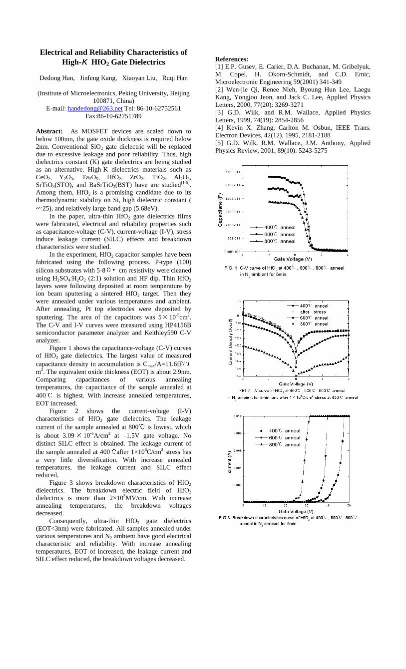
Figure 1 shows the capacitance-voltage (C-V) curves of HfO2 gate dielectrics. The largest value of measured capacitance density in accumulation is Cmax/A=11.6fF/ �m2. The equivalent oxide thickness (EOT) is about 2.9nm. Comparing capacitances of various annealing temperatures, the capacitance of the sample annealed at 400 � is highest. With increase annealed temperatures, EOT increased.
Figure 2 shows the current-voltage (I-V) characteristics of HfO2 gate dielectrics. The leakage current of the sample annealed at 800� is lowest, which is about 3.09 � 10-6A/cm2 at –1.5V gate voltage. No distinct SILC effect is obtained. The leakage current of the sample annealed at 400 � after 1×10⁶C/cm2 stress has a very lit tle diversification. With increase annealed temperatures, the leakage current and SILC effect reduced.
Figure 3 shows breakdown characteristics of HfO2 dielectrics. The breakdown electric field of HfO2 dielectrics is more than 2×10⁵MV/cm. With increase annealing temperatures, the breakdown voltages decreased.
Consequently, ultra-thin HfO2 gate dielectrics (EOT<3nm) were fabricated. All samples annealed under various temperatures and N2 ambient have good electrical characteristic and reliabili ty. With increase annealing temperatures, EOT of increased, the leakage current and SILC effect reduced, the breakdown voltages decreased.
References: [1] E.P. Gusev, E. Carier, D.A. Buchanan, M. Gribelyuk, M. Copel, H. Okorn-Schmidt, and C.D. Emic, Microelectronic Engineering 59(2001) 341-349 [2] Wen-jie Qi, Renee Nieh, Byoung Hun Lee, Laegu Kang, Yongjoo Jeon, and Jack C. Lee, Applied Physics Letters, 2000, 77(20): 3269-3271 [3] G.D. Wilk, and R.M. Wallace, Applied Physics Letters, 1999, 74(19): 2854-2856 [4] Kevin X. Zhang, Carlton M. Osbun, IEEE Trans. Electron Devices, 42(12), 1995, 2181-2188 [5] G.D. Wilk, R.M. Wallace, J.M. Anthony, Applied Physics Review, 2001, 89(10): 5243-5275


