
EG1103 Electrical Engineering
Ben M. ChenAssociate Professor
Office: E4-6-7Phone: 874-2289
Email: [email protected]://vlab.ee.nus.edu.sg/~bmchen
Copyrighted by Ben M. Chen1

Lecture Format & Course Outlines
Copyrighted by Ben M. Chen2
text
book
or
lecture
notes
Copyrighted by Ben M. Chen3

Electrical Engineering
Well known electrical engineering companies:
• Singapore Telecom (largest in Singapore)
• Creative Technology (largest manufacturer of PC sound boards)
• Disk Drive Companies (largest producer of PC hard disk Drives)
“Yan can Cook”:
• Ingredients + Recipe + (Funny Talk) = Good Food
Electrical Systems:
• Components + Method + (Funny Talk) = Good Electrical System
EG1103 Module:
• To introduce basic electrical components & analysis methods.
Copyrighted by Ben M. Chen4

Reference Textbooks
• D. E. Johnson, J. R. Johnson and J. L. Hilburn, Electric
Circuits Analysis, 2nd Ed., Prentice Hall, 1992.
• S. A. Boctor, Electric Circuits Analysis, 2nd Ed., Prentice
Hall, 1992.
Copyrighted by Ben M. Chen5

Lectures
Lectures will follow closely (but not 100%) the materials in
the textbook.
However, certain parts of the textbook will not be covered
and examined and this will be made known during the
classes.
Attendance is essential.
ASK any question at any time during the lecture.
Copyrighted by Ben M. Chen6

Tutorials
The tutorials will start on Week 4 of the semester. (Week 1 corresponds
to the Orientation Week.)
Although you should make an effort to attempt each question before the
tutorial, it is NOT necessary to finish all the questions.
Some of the questions are straightforward, but quite a few are difficult
and meant to serve as a platform for the introduction of new concepts.
ASK your tutor any question related to the tutorials and the course.
Copyrighted by Ben M. Chen7

Examination
The examination paper is 2-hour in duration.
You will be provided with a list of important results. This list is given
under “Summary of Important Results” in the Appendix of the textbook.
To prepare for the examination, you may wish to attempt some of the
questions in examinations held in previous years. These papers are
actually the Additional Problems in the Appendix of the textbook (no
solutions to these problems will be given out to the class).
However, note that the topics covered may be slightly different and
some of the questions may not be relevant. Use your own judgement to
determine the questions you should attempt.
Copyrighted by Ben M. Chen8

Mid-term Test
There will be an one-hour (actually 50 minutes) test. It will be given
some time around mid-term (most likely after the recess week). The
test will consists 15% of your final grade, i.e., your final grade in this
course will be computed as follows:
Your Final Grade = 15% of Your Mid-term Test Marks (max. = 100)
+ 85% of Your Examination Marks (max = 100)
Copyrighted by Ben M. Chen9

Outline of the Course1. DC Circuit Analysis
SI Units. Voltage, current, power and energy. Voltage and current
sources. Resistive circuits. Kirchhoff's voltage and current laws. Nodal
and mesh analysis. Ideal and practical sources. Maximum power
transfer. Thevenin’s and Norton’s equivalent circuits. Superposition.
Dependent sources. Introduction to non-linear circuit analysis.
2. AC Circuits
Root mean square value. Frequency and phase. Phasor. Capacitor and
Inductor. Impedance. Power. Power factor. Power factor improvement.
Frequency response. Tune circuit. Resonance, bandwidth and Q factor.
Periodic signals. Fourier series.
Copyrighted by Ben M. Chen10

Outline of the Course (Cont.)
3. Transient
First order RL and RC circuits. Steady state and transient responses.
Time constant. Voltage and current continuity. Second order circuit.
4. Magnetic Circuit
Magnetic flux and mmf. Ampere’s law. Force between surfaces.
Transformers.
5. Electrical Measurement
Current and voltage measurement. Common instruments. Oscilloscope.
Copyrighted by Ben M. Chen11

Web-based Virtual Labsare now on-line
Developed by: CC Ko and Ben M. Chen
• Have you ever missed your experiments?
• Do you have problems with your lab schedule?
• Do you have problems in getting results for your report?
Visit newly developed web-based virtual labs available from
5:00pm to 8:00am at http://vlab.ee.nus.edu.sg/vlab/
Copyrighted by Ben M. Chen12

Chapter 1. SI Units
Copyrighted by Ben M. Chen13

1.1 Important Quantities and Base SI Units
Length m etre mM ass, m kilogram kgTim e, t second sElectric current, i am pere ATherm odynam ic tem perature kelvin KPlane angle radian rad
Copyrighted by Ben M. Chen14
Chapter 2. DC Circuit Analysis
Copyrighted by Ben M. Chen15

2.1 Voltage Source
Two common dc (direct current) voltage sources are:
Dry battery (AA, D, C, etc.)
Lead acid battery in car
Regardless of the load connected and the current drawn, the above sources
have the characteristic that the supply voltage will not change very much.
The definition for an ideal voltage source is thus one whose output voltage
does not depend on what has been connected to it. The circuit symbol is
v
Copyrighted by Ben M. Chen16

Basically, the arrow and the value signifies that the top terminal has a
potential of v with respect to the bottom terminal regardless of what has
been connected and the current being drawn.
Note that the current being drawn is not defined but depends on the load
connected. For example, a battery will give no current if nothing is
connected to it, but may be supplying a lot of current if a powerful motor
is connected across its terminals. However, in both cases, the terminal
voltages will be roughly the same.
Copyrighted by Ben M. Chen17

Using the above and other common circuit symbol, the following are
identical:
1.5 V 1.5 V− 1.5 V
+
−
1.5 V+
−
Note that on its own, the arrow does not correspond to the positive
terminal. Instead, the positive terminal depends on both the arrow and
the sign of the voltage which may be negative.
Copyrighted by Ben M. Chen18

2.2 Current Source
In the same way that the output voltage of an ideal voltage source does
not depend on the load and the current drawn, the current delivers by an
ideal current source does not depend on what has been connected and
the voltage across its terminals. Its circuit symbol is
i
Note that ideal voltage and current sources are idealisations and do not
exist in practice. Many practical electrical sources, however, behave like
ideal voltage and current sources.
Copyrighted by Ben M. Chen19

2.3 Power and Energy
Consider the following device,
v
i
DevicePower Consumed
by Device = vip
In 1 second, there are i charges passing through the device. Their electric
potential will decrease by v and their electric potential energy will decrease
by iv. This energy will have been absorbed or consumed by the device.
The power or the rate of energy consumed by the device is thus p = i v.
Copyrighted by Ben M. Chen20
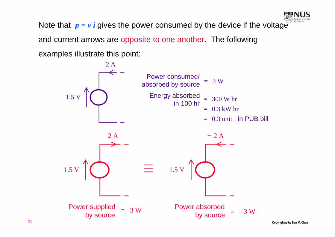
Note that p = v i gives the power consumed by the device if the voltage
and current arrows are opposite to one another. The following
examples illustrate this point:
1.5 V
2 A
Energy absorbed = 300 W hr= 0.3 kW hr
0.3 unit= in PUB bill
absorbed by source = 3 WPower consumed/
in 100 hr
1.5 V
2 A
Power supplied = 3 Wby source
1.5 V
2 A−
by source = 3 WPower absorbed
−Copyrighted by Ben M. Chen21

2.4 Resistor
The symbol for an ideal resistor is
v
i
R
Provided that the voltage and current arrows are in opposite directions,
the voltage-current relationship follows Ohm's law:
iRv =The power consumed is
RvRivip
22 ===
Common practical resistors are made of carbon film, wires, etc.
Copyrighted by Ben M. Chen22

2.5 Relative Power
Powers, voltages and currents are often measured in relative terms
with respect to certain convenient reference values. Thus, taking
mW 1=refp
as the reference (note that reference could be any value), the powerW2=p
will have a relative value of
2000W10
W2mW1
W23- ===
refpp
The log of this relative power or power ratio is usually taken and given
a dimensionless unit of bel. The power p = 2 W is equivalent to
( ) ( ) ( ) bel3.32log1000log2000loglog =+==⎟⎟⎠
⎞⎜⎜⎝
⎛
refpp
Copyrighted by Ben M. Chen23
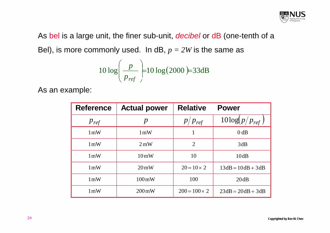
As bel is a large unit, the finer sub-unit, decibel or dB (one-tenth of a
Bel), is more commonly used. In dB, p = 2W is the same as
( ) dB332000log10log10 ==⎟⎟⎠
⎞⎜⎜⎝
⎛
refpp
As an example:
Reference Actual power Relative Power
refp p refpp ( )refpplog101mW 1mW 1 dB0
1mW 2 mW 2 3dB
1mW 10mW 10 10dB
1mW 20mW 20 10 2= × 13 10 3dB dB dB= +
1mW 100mW 100 20dB
1mW 200mW 200 100 2= × 23 20 3dB dB dB= +
Copyrighted by Ben M. Chen24

Although dB measures relative power, it can also be used to measure
relative voltage or current which are indirectly related to power.
For instance, taking V1.0=refv
as the reference voltage (again reference voltage could be any value),
the power consumed by applying vref to a resistor R will be
Rv
p refref
2
=
Similarly, the voltage
V1=v
will lead to a power consumption of Rvp
2=
Copyrighted by Ben M. Chen25
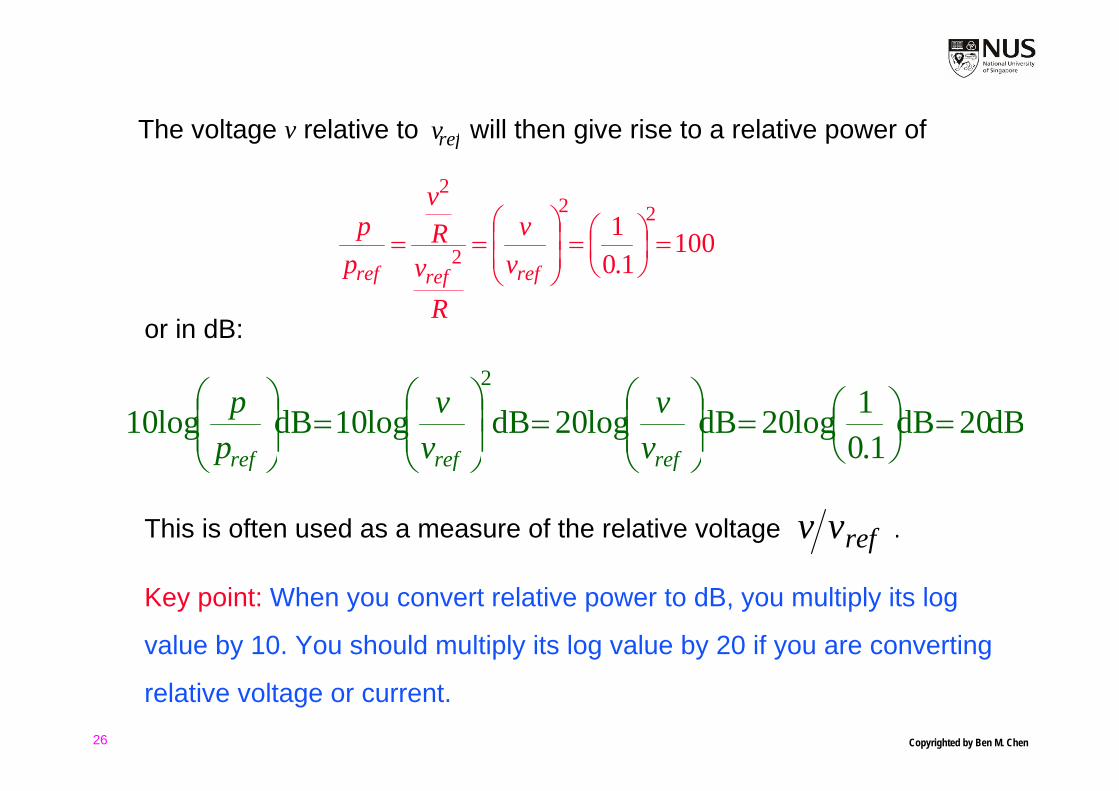
The voltage v relative to will then give rise to a relative power ofrefv
1001.0
1 22
2
2
=⎟⎠⎞
⎜⎝⎛=⎟
⎟⎠
⎞⎜⎜⎝
⎛==
refrefref vv
Rv
Rv
pp
or in dB:
dB20dB1.0
1log20dBlog20dBlog10dBlog102
=⎟⎠⎞
⎜⎝⎛=⎟
⎟⎠
⎞⎜⎜⎝
⎛=⎟
⎟⎠
⎞⎜⎜⎝
⎛=⎟
⎟⎠
⎞⎜⎜⎝
⎛
refrefref vv
vv
pp
This is often used as a measure of the relative voltage .refvv
Key point: When you convert relative power to dB, you multiply its log
value by 10. You should multiply its log value by 20 if you are converting
relative voltage or current.
Copyrighted by Ben M. Chen26

As an example:
Reference Actual voltage Relative Voltage
refv v refvv ( )refvvlog200 1. V 0 1. V 1 dB00 1. V 0 1 2. V 2 dB30 1. V 0 2. V 2 2 2= × dB3dB3dB6 +=
0 1. V 0 1 10. V 10 dB100 1. V 0 1 20. V 20 10 2= × dB3dB10dB13 +=
0 1. V 1V 10 10 10= × dB10dB10dB20 +=
The measure of relative current is the same as that of relative voltage and
can be done in dB as well.
Copyrighted by Ben M. Chen27

The advantage of measuring relative power, voltage and current in
dB can be seen from considering the following voltage amplifier:
Amplifier
v v2Voltagegain
2 = 6 dB
The voltage gain of the amplifier is given in terms of the output voltage
relative to the input voltage or, more conveniently, in dB:
( ) dB6dB2log2022====
vvg
Copyrighted by Ben M. Chen28

If we cascade 3 such amplifiers with different voltage gains together:
v v2 v28v2.8
Amplifier
Voltagegain
2 = 6 dB
Amplifier
Voltagegain
1.4 = 3 dB
Amplifier
Voltagegain
10 = 20 dB
the overall voltage gain will be28104.12 =××=totalg
However, in dB, it is simply:
dB29dB20dB3dB6 =++=totalg
Under dB which is log based, multiplication's become additions.
Copyrighted by Ben M. Chen29
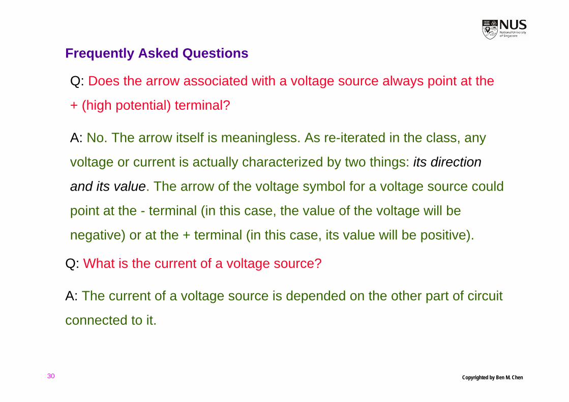
Frequently Asked Questions
Q: Does the arrow associated with a voltage source always point at the
+ (high potential) terminal?
A: No. The arrow itself is meaningless. As re-iterated in the class, any
voltage or current is actually characterized by two things: its direction
and its value. The arrow of the voltage symbol for a voltage source could
point at the - terminal (in this case, the value of the voltage will be
negative) or at the + terminal (in this case, its value will be positive).
Q: What is the current of a voltage source?
A: The current of a voltage source is depended on the other part of circuit
connected to it.
Copyrighted by Ben M. Chen30

Q: Does a volt source always supply power to other components in a circuit?
A: NO. A voltage source might be consuming power if it is connected to a
circuit which has other more powerful sources. Thus, it is a bad idea to pre-
determine whether a source is consuming power or supplying power. The
best way to determine it is to follow the definition in our text and computer
the power. If the value turns out to be positive, then the source will be
consuming power. Otherwise, it is supplying power to the other part of the
circuit.
Q: Is the current of a voltage source always flowing from + to - terminals?
A: NO. The current of a voltage source is not necessarily flowing from the
positive terminal to the negative terminal.
Frequently Asked Questions
Copyrighted by Ben M. Chen31

Frequently Asked Questions
Q: What is the voltage cross over a current source?
A: It depends on the circuit connected to it.
Q: Is the reference power (or voltage, or current) in the definition of the
relative power (or voltage, or current) unique?
A: No. The reference power (voltage or current) can be any value.
Remember that whenever you deal with the relative power (voltage or
current), you should keep in your mind that there are a reference power
(voltage or current) and an actual power (voltage or current) associated
with it.
Copyrighted by Ben M. Chen32

2.6 Kirchhoff's Current Law (KCL)
As demonstrated by the following examples, this states that the
algebraic sum of the currents entering/leaving a node/closed surface
is 0 or equivalently to say that the total currents flowing into a node is
equal to the total currents flowing out from the node.
i i
iii
1
23
4
5 i i
iii
1
23
4
5
054321 =++++ iiiii for both cases.
Since current is equal to the rate of flow of charges, KCL actually
corresponds to the conservation of charges.
Copyrighted by Ben M. Chen33

2.7 Kirchhoff's Voltage Law (KVL)
As illustrated below, this states that the algebraic sum of the voltage
drops around any close loop in a circuit is 0.
v5
v 1
v4
v3
v2
054321 =++++ vvvvv
(note that all voltages are in the same direction)
Since a charge q will have its electric potential changed by qv1, qv2,
qv3, qv4 , qv5 as it passes through each of the components, the total
energy change in one full loop is q ( v1 + v2 + v3 + v4 + v5 ). Thus, from
the conservation of energy: 054321 =++++ vvvvv
Copyrighted by Ben M. Chen34

2.8 Series Circuit
Consider 2 resistors connected in series:
v
i
R
1
R
2v
21
v
11 Riv = 22 Riv = 21 vvv +=
the voltage-current relationship is ( )21 RRiv +=
By KVL: - v + v1 + v2 = 0
Now consider
v
i
R1 R2+
the voltage-current relationship is ( )21 RRiv +=
Copyrighted by Ben M. Chen35

Since the voltage/current relationships are the same for both circuits,
they are equivalent from an electrical point of view. In general, for n
resistors R1, ..., Rn connected in series, the equivalent resistance R is
nRRR ++= L1
Clearly, the resistance's of resistors connected in series add (Prove it).
Copyrighted by Ben M. Chen36

2.9 Parallel Circuit
Consider 2 resistors connected in parallel:
v
R
R2
1
i
i
i
1
2
11 R
vi =
22 R
vi =
⎟⎟⎠
⎞⎜⎜⎝
⎛+=+=
2121
11RR
viii
Clearly, the parallel circuit is equivalent to a resistor R with voltage/current
relationship
Rvi = with
21
111RRR
+=
Copyrighted by Ben M. Chen37

In general, for n resistors R1, …, Rn, connected in parallel, the equivalent
resistance R is given by
nRRR111
1++= L
Note that 1/R is often called the conductance of the resistor R. Thus,
the conductances of resistors connected in parallel add.
Copyrighted by Ben M. Chen38

2.10 Voltage Division
Consider 2 resistors connected in series:
v
i
R1
R2
v1
v2
21 RRvi+
= vRR
RiRv ⎟⎟⎠
⎞⎜⎜⎝
⎛+
==21
111
vRR
RiRv ⎟⎟⎠
⎞⎜⎜⎝
⎛+
==21
222
2
1
2
1RR
vv
=
Thus,The total resistance of the circuit is R1 + R2.
Copyrighted by Ben M. Chen39

2.11 Current Division
Consider 2 resistors connected in parallel:
v
i
R1 R2
i 1i2
The total conductance of the circuit is21
111RRR
+=
while the equivalent resistance is
21
11RR
iRiv+
==
iRR
Ri
RR
RRvi ⎟⎟
⎠
⎞⎜⎜⎝
⎛+
=
⎟⎟⎟⎟
⎠
⎞
⎜⎜⎜⎜
⎝
⎛
+==
21
2
21
1
11 11
1
iRR
Ri
RR
RRvi ⎟⎟
⎠
⎞⎜⎜⎝
⎛+
=
⎟⎟⎟⎟
⎠
⎞
⎜⎜⎜⎜
⎝
⎛
+==
21
1
21
2
22 11
1
Thus,
1
2
2
1
RR
ii
=
Copyrighted by Ben M. Chen40

2.12 Ladder Circuit
Consider the following ladder circuit:
2
3
4
5
The equivalent resistance can be
determined as follows:
3
4
5 ||||2
5 4+(3 ||||2)
||||5 [4+(3||||2)]
The network is equivalent to a
resistor with resistance
( )[ ]( )
21
31
14
151
1
2341
51
12345
++
+=
++
=+=
||
||||R
Copyrighted by Ben M. Chen41

2.13 Branch Current Analysis
Consider the problem of determining the equivalent resistance of the following
bridge circuit:
4
2 4
23
Since the components are not connected in straightforward series or parallel
manner, it is not possible to use the series or parallel connection rules to
simplify the circuit. However, the voltage-current relationship can be
determined and this will enables the equivalent resistance to be calculated.
One method to determine the voltage-current relationship is to use the branch
current method.Copyrighted by Ben M. Chen42

4
2 4
23
v
i
=iv
Equivalent Resistance
i1
i2
1. Assign branch currents (with
any directions you prefer so
that currents in other branches
can be found)
1ii −
21 iii −− 21 ii +2. Find all other branch currents
(with any directions you prefer)
(Use KCL to find them)
12 i
)(4 21 ii +)(2 21 iii −−
)(4 1ii −
3. Write down branch voltages
23 i
4. Identify independent loops
KVL: 21211 46)(42 iiiiiv +=++=
KVL: 121 23)(4 iiii =+−
)(23)(4 21221 iiiiii −−=++KVL:
Eliminate i1 and i2,
127
1ii =
62ii −= iv
617
=
Branch Current Analysis: Example One
Copyrighted by Ben M. Chen43

Branch Current Analysis: Example Two
2
3
4
12 A 1 V
1. Assign branch currents
(so that currents in other
branches can be found).
1i 2i
12 i− 21 ii −
2
2. Find all other branch
currents (KCL)
12 i− )(3 21 ii −
14i 22i
3. Write down voltages across components
KVL: )(321 212 iii −=+
KVL: )(342 2111 iiii −+=−
This implies:
⎥⎦
⎤⎢⎣
⎡=⎥
⎦
⎤⎢⎣
⎡⎥⎦
⎤⎢⎣
⎡−−
⇒=−=−
21
3853
238153
2
1
21
21
ii
iiii
⎥⎦
⎤⎢⎣
⎡−
=⎥⎦
⎤⎢⎣
⎡⎥⎦
⎤⎢⎣
⎡−−
=⎥⎦
⎤⎢⎣
⎡⇒
−
27
311
21
3853 1
2
1
ii
4. Identify independent loops
(ex. 2A branch)
Copyrighted by Ben M. Chen44

4
2 4
23
v
2.14 Mesh (Loop Current) Analysis
i
ai
bi
1. Assign fictitious loop currents.i
ai
biab ii −
iib −
iia −
2. Find branch currents (KCL)ai2
bi4)(2 iib −
)(4 iia −
)(3 ab ii − 3. Write down branch voltages
4. Identify independent loops
KVL: ba iiv 42 +=
02)(3)(4 =+−−− aaba iiiiiKVL:
KVL: 0)(34)(2 =−++− abbb iiiii
5. Simplify the equations
obtained, we get
617
617
=⇒= eequivalencRiv
Copyrighted by Ben M. Chen45

2
3
4
12 A 1 V
2.15 Nodal Analysis
A B
aV bV
1. Assign nodal voltage w.r.t. the reference node
ba VV − bV−1 2. Find branch voltages (KVL)
3. Determine
branch currents
2
4ba VV −
21 bV−
aV 3bV
4. Apply KCL to Nodes A & B
Node A:
42 ba
aVVV −
+=
Node B:
321
4bbba VVVV
=−
+−
⇐−=−
=−6133
85
ba
ba
VVVV
⇐⎥⎦
⎤⎢⎣
⎡−
=⎥⎦
⎤⎢⎣
⎡⎥⎦
⎤⎢⎣
⎡−−
68
13315
b
a
VV
⇒ 3155
=aV3127
=bV
Copyrighted by Ben M. Chen46

2.16 Practical Voltage Source
An ideal voltage source is one whose
terminal voltage does not change
with the current drawn. However, the
terminal voltages of practical sources
usually decrease slightly as the
currents drawn are increased.
A commonly used model for a
practical voltage source is:
To represent it as a series of an ideal
voltage source & an internal
resistance.
voc
R in
Model for voltage source
v
Practical voltage source
i
R load
R loadv
i
⇐+= inoc iRvvCopyrighted by Ben M. Chen47

When or when the source is short circuited so that :0=loadR 0=v
voc
R in
v
i =voc
R in
R load = 0= 0Short circuit
When or when the source is open circuited so that :∞=loadR 0=i
voc
R in
i = 0
v = voc R load = ∞Open circuit
Copyrighted by Ben M. Chen48

Graphically:
voc
v
i0
=Slope R in
in
oc
Rv
Good practical voltage source should therefore have small internal
resistance, so that its output voltage will not deviate very much from the
open circuit voltage, under any operating condition.
The internal resistance of an ideal voltage source is therefore zero so that
does not change with .
vi
Copyrighted by Ben M. Chen49

To determine the two parameters and that characterize, say, a
battery, we can measure the output voltage when the battery is open-
circuited (nothing connected except the voltmeter). This will give .
Next, we can connect a load resistor and vary the load resistor such
that the voltage across it is . The load resistor is then equal to :
ocvinR
ocv
2ocv
inR
voc
R in
R loadv
i
= R in=voc
2
voc
2
Copyrighted by Ben M. Chen50

2.17 Maximum Power Transfer
Consider the following circuit:
voc
R in
Model for voltage source
R loadv
i
The current in the load resistor is
loadin
oc
RRvi+
=
This is always positive. However, if
The power absorbed by the
load resistor is
( )2
22
loadin
loadocloadload RR
RvRip+
==
0=loadR or .0, =∞= loadload PR
0 Rload
pload
Copyrighted by Ben M. Chen51

Differentiating:
( ) ( ) ( ) ⎥⎦
⎤⎢⎣
⎡
+−
=⎥⎦
⎤⎢⎣
⎡
+−
+= 3
232
2 21
loadin
loadinoc
loadin
load
loadinoc
load
load
RRRRv
RRR
RRv
dRdp
The load resistor will be absorbing the maximum power or the source will be
transferring the maximum power if the load and source internal resistances
are matched, i.e., . The maximum power transferred is given byloadin RR =
in
oc
Rvp
4
2
loadmax =( )
⇒+
== 2
22
loadin
loadocloadload RR
RvRip
0 Rload
pload
Rin
vocRin4
2 When the load absorbs the maximum
power from the source, the overall
power efficiency of 50%, which is too
low for a usual electric system.Copyrighted by Ben M. Chen52

Why is the electric power transferred from power stations to local stations
in high voltages?
( )2
22 KW300
vRRiP w
wloss ==
Power
Station load
resistance in wire
wR
vi KW300=KW300=P
v
Power loss in the transmission line:
The higher voltage v is transmitted, the less power is lost in the wire.
Copyrighted by Ben M. Chen53

2.18 Practical Current Source
An ideal current source is one which delivers a constant current regardless
of its terminal voltage. However, the current delivered by a practical
current source usually changes slightly depending on the load and the
terminal voltage.
A commonly used model for a current source is:
isc R in
Model for current source
R loadv
i
iRvi
insc +=⇒
Copyrighted by Ben M. Chen54

When or when the source is short-circuited so that :0=loadR 0=v
isc R in
i = isc
0
v = 0 R load = 0Short circuit
Graphically:v
i0
=Slope R in
isc
Good practical current source should therefore
have large internal resistance so that the current
delivered does not deviate very much from the
short circuit current under any operating
condition.
The internal resistance of an ideal current source is
therefore infinity so that i does not change with v.Copyrighted by Ben M. Chen55

2.19 Thevenin's Equivalent Circuit
v
iComplicated circuit
with linear elements
such as resistors,
voltage/current sources
voc R inv i= +
voc R inv i= +voc
R in
v
i
Thevenin's equivalent circuit
Key points:
1. The black box
(i.e., the part of the
circuit) to be
simplified must be
linear.
2. The black box
must have two
terminals
connected to the
rest of the circuit.
Complicated circuit
with linear elements
such as resistors,
voltage/current sources
Copyrighted by Ben M. Chen56
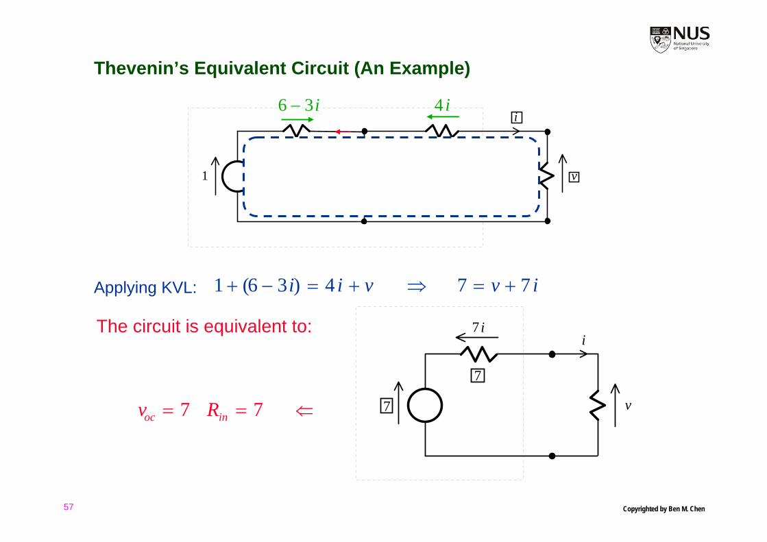
Thevenin’s Equivalent Circuit (An Example)
4
21 v
i
3 i−2
i36 − i4
Applying KVL: ivvii 774)36(1 +=⇒+=−+
The circuit is equivalent to:
v
i
7
7
7 i
⇐== 77 inoc Rv
Copyrighted by Ben M. Chen57

Alternatively, note that from the Thevenin's
equivalent circuit:
voc
Rin
Open circuit voltage voc=
Rin Resistance seen with=source replace by
internal resistanceRin
⇒
4
21
3
02
60
voc= 7
43
Rin= 77
7
Short Circuit
Copyrighted by Ben M. Chen58

2.20 Norton's Equivalent Circuit
R inv i= +
voc R inv i= +voc
R in
v
i
Thevenin's equivalent circuit
isc R in
Norton's equivalent circuit
iscR in
if voc iscR in= if voc iscR in=
v
i
R in
v i= +isc
It is simple to see
that if we let
inscoc Riv =
then the
relationships of
voltage/current for
both Thevenin’s
and Norton’s
equivalent circuits
are exactly the
same.
Copyrighted by Ben M. Chen59

From the Norton's equivalent circuit, the two parameters and
can be obtained from:sci inR
Short circuit currenti sc R in
i
=v 0
= i sc
= i sc
R in
Resistance seen with=source replace by
internal resistanceR in
Open Circuit
Copyrighted by Ben M. Chen60

Example: Reconsider the circuit The Norton's equivalent
circuit is therefore:
1 7
And the Thevenin's equivalent
circuit is:
7
7
21
43
21
3
2
0
isc
4
isc4isc−
6−3isc
43
Rin = 7
1 6− 3isc isc4+ = 1isc =or
Copyrighted by Ben M. Chen61

Summary on how to find an equivalent circuit:
Step 1. Identify the circuit or a portion of a complicated circuit that is to be
simplified. Be clear in your mind on which two terminals are to be
connected to the other network.
Step 2. Short-circuit all the independent voltage sources and open-circuit
all independent current sources in the circuit that you are going to simplify.
Then, find the equivalent resistance w.r.t. the two terminals identified in
Step 1.
Step 3. Find the open circuit voltage at the output terminals (for Thevenin’s
equivalent circuit) or the short circuit current at the output terminals (for
Norton’s equivalent circuit).
Step 4. Draw the equivalent circuit (either the Thevenin’s or Norton’s one).
Copyrighted by Ben M. Chen62

More Example For Equivalent Circuits:
i R vR
R R
1i
1R2
vR
R R
1i
1
i v
R R
1i
R
R2
2
1
vR
R R
1i
1
vR
R R1
v
R2
2
i v
R R
1i
R
R2
2
1
Copyrighted by Ben M. Chen63

2.21 Superposition
Consider finding in the circuit:sci
3
isc
4
1 2
By using the principle of super-
position, this can be done by finding
the components of due to the 2
independent sources on their own
(with the other sources replaced by
their internal resistances):
sci
1
43
1/7
2
3 4
2(3/7)2(4/7)24/7 24/7
2(3/7) (1/7)
3 4
1 2
= + = 1isc
Open circuit
Short circuit
Copyrighted by Ben M. Chen64

Linear Systems and Superposition
Linear Systemin1
in2
Out = 6 in1 + 7 in2
(the definition of the
linear system)
Linear System16
06 (16) = 96
Linear System0
277 (27) = 189
Linear System16
2796 + 189 = 285
Note that:
Linear system: linear
relationship between
inputs and outputs
Superposition:
Applicable only to
linear systems
Copyrighted by Ben M. Chen65
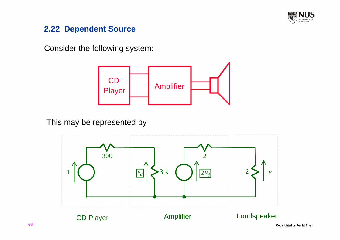
2.22 Dependent Source
Consider the following system:
CDPlayer Amplifier
This may be represented by
1 v
300
CD Player Amplifier Loudspeaker
23 kvd 2vd
2
Copyrighted by Ben M. Chen66

Note that the source in the Amplifier block is a dependent source. Its
value depends on , the voltage across the inputs of the amplifier. Using
KCL and KVL, the voltage can be easily found:dv
v
33001
vd = 1110 2vd = 11
201 v
300
23 k
2
115
= 1110
However, if we use the principle of superposition treating the dependent
source as an independent source (which is wrong !), the value of v will be 0:
Copyrighted by Ben M. Chen67

0
vd = 0 20
300
23 k
2
0
0
33001
vd = 1110 01
300
23 k
2
0
0
vd = 0
Dependent sources, which depend on other voltages/currents in the circuit
and are therefore not independent excitations, cannot be removed when
the principle of superposition is used. They should be treated like other
passive components such as resistors in circuit analysis.Copyrighted by Ben M. Chen68

Topics Skipped
• Nonlinear Circuit
• Delta Circuit
• Star Circuit
• All these topics are not examinable in test and examination.
Copyrighted by Ben M. Chen69

Reading Assignment
• Appendix C.1. Matrix Algebra
• Appendix C.2. Complex Number
• Appendix C.3. Linear Differential Equation
Copyrighted by Ben M. Chen70

Chapter 3. AC Circuit Analysis
Copyrighted by Ben M. Chen71

Appendix Materials: Operations of Complex Numbers
Coordinates: Cartesian Coordinate and Polar Coordinate⎟⎠⎞
⎜⎝⎛−
+==+ 125tan
2239.01
51213512j
j eejreal part imaginary part magnitude argument
Euler’s Formula: )sin()cos( θθθ je j +=
Additions: It is easy to do additions (subtractions) in Cartesian coordinate.
)()()()( wbjvajwvjba +++=+++
Multiplication's: It is easy to do multiplication's (divisions) in Polar coordinate.
)()( ωθωθ +=•jjj eruuere )( ωθ
ω
θ−= j
j
j
eur
uere
Copyrighted by Ben M. Chen72

3.1 AC Sources
Voltages and currents in DC circuit are constants and do not change with
time. In AC (alternating current) circuits, voltages and currents change with
time in a sinusoidal manner. The most common ac voltage source is the
mains:
230 2
150
t
π2 500.4( )
−
( ) ( ) ( ) ⎟⎠⎞
⎜⎝⎛ +=+=+= θπθωθπ
Ttrtrftrtv 2cos2cos22cos2
( )4.0100cos2230 += tπ
rad4.0== phaseθ
Hz50== frequencyf
srad3141002 ==== ππω frequencyangularf
s02.05011
==== periodf
T
V32422302 === value peakr
V230== valuesquare)mean(rootrmsrCopyrighted by Ben M. Chen73

r 2
t
How to find the phase for a sinusoidal function?
)cos(2)( trtv ω=
a−
)cos(2
])[cos(2)(
atr
atrtv
ωω
ω
+=
+=
4.0)50(2
4.0314 =⎟⎟⎠
⎞⎜⎜⎝
⎛==
πωθ a
for previous example.
aωθ =Phase
πθπ ≤≤−
Copyrighted by Ben M. Chen74

3.2 Phasor
A sinusoidal voltage/current is represented using complex number format:
The advantage of this can be seen if, say, we have to add 2 sinusoidal
voltages given by:
)sin()cos( ωωω je j +=Euler’s Formula:
( ) ⎟⎠⎞
⎜⎝⎛ +=
6cos231
πωttv ( ) ⎟⎠⎞
⎜⎝⎛ −=
4cos252
πωttv
( ) ( )⎥⎥⎦
⎤
⎢⎢⎣
⎡⎟⎟⎠
⎞⎜⎜⎝
⎛=⎟
⎠⎞
⎜⎝⎛ += tjj
eettv ωππω 23Re
6cos23 6
1 ( ) ( )⎥⎥⎦
⎤
⎢⎢⎣
⎡⎟⎟⎠
⎞⎜⎜⎝
⎛=⎟
⎠⎞
⎜⎝⎛ −=
− tjjeetv ω
ππω 25Re4
cos25 42
( ) ( ) ( )[ ] ( )( )[ ]tjjtj ereertrtv ωθθωθω 2ReRe2cos2 ==+= +
( ) ( ) ( ) ( )( )[ ]tjjtjjeeeeetvtv ωω
ππ
247.6Re253Re 32.04621
−−=
⎥⎥⎦
⎤
⎢⎢⎣
⎡⎟⎟⎠
⎞⎜⎜⎝
⎛+=+ ( )32.0cos247.6 −= tω
Copyrighted by Ben M. Chen75

Note that the complex time factor appears in all the expressions.
If we represent and by the complex numbers or phasors:
tje ω2
( )tv1 ( )tv2
( ) ⎟⎠⎞
⎜⎝⎛ +==
6cos233 1
61
πωπ
ttveVj
ngrepresenti
( ) ⎟⎠⎞
⎜⎝⎛ −==
−
4cos255 2
42
πωπ
ttveVj
ngrepresenti
then the phasor representation for will be( ) ( )tvtv 21 +
ngrepresenti32.04621 47.653 jjj
eeeVV −−=+=+
ππ
( ) ( ) ( )32.0cos247.621 −=+ ttvtv ω
)sin()cos( ωωω je j +=Euler’s Formula:
32.046 47.603.214.64
sin4
cos56
sin6
cos353 jjjejjjee −−
=−=⎟⎠
⎞⎜⎝
⎛⎟⎠⎞
⎜⎝⎛−+⎟
⎠⎞
⎜⎝⎛−+⎟
⎠
⎞⎜⎝
⎛⎟⎠⎞
⎜⎝⎛+⎟
⎠⎞
⎜⎝⎛=+
ππππππ
Copyrighted by Ben M. Chen76

By using phasors, a time-varying ac voltage
( ) ( ) ( ) ( )[ ]tjj eretrtv ωθθω 2Recos2 =+=
becomes a simple complex time-invariant number/voltage θrV = rejθ =
( )tvVVr of value r.m.s. of modulusmagnitude/ ===
[ ] VV ofphase== ArgθGraphically, on a phasor diagram:
V
Imag
Real0θ
r
Complex Plane
Using phasors, all time-varying ac quantities
become complex dc quantities and all dc circuit
analysis techniques can be employed for ac
circuit with virtually no modification.
Copyrighted by Ben M. Chen77

Example:4
6 3 2cos )+ 0.1( tω5 2cos )− 0.2( tω
i )( t
4
65 j- 0.2e
I
3 j 0.1e
46
30 j- 0.2e
I
3 j 0.1e
Thevenin's equivalent circuitfor current soure and 6 Ω resistor Copyrighted by Ben M. Chen78

46
30 j- 0.2e 3 j 0.1e
I 30 j- 0.2e 3 j 0.1e−10
= = 2.64 − j0.63 = 2.71e j 0.23-
[ ] [ ]
23.0641.2626.0tan
22
1.02.0
71.2626.0641.2
626.0641.2)030.0299.0()596.0940.2(1.0sin1.0cos3.0)2.0sin()2.0cos(3
10330
1
jj
jj
ee
jjjjj
eeI
−⎟⎠⎞
⎜⎝⎛ −
−
=+=
−=+−−=+−−+−=
−=
−
)23.0cos(271.2)( −=⇒ tti ωCopyrighted by Ben M. Chen79

3.3 Root Mean Square (rms) Value
For the ac voltage
( ) ( ) ⎟⎠⎞
⎜⎝⎛ +=+= θπθπ
Ttrftrtv 2cos22cos2
( ) ( ) 1cos22cos 2 −= xx
( ) ⎥⎦⎤
⎢⎣⎡
⎟⎠⎞
⎜⎝⎛ ++=⎟
⎠⎞
⎜⎝⎛ += θπθπ 24cos12cos2 2222
Ttr
Ttrtv
2
T
r
tπ2
− Tθ
t
2 r2
v )( t
v )( t2
The average or mean of the square value is
( ) ( ) =∫=∫T dttv
Tdttv 0
21
2 11
1period period
20
20
2 124cos11 rdtrT
dtT
trT
TT =∫=∫ ⎥⎦⎤
⎢⎣⎡
⎟⎠⎞
⎜⎝⎛ ++ θπ
The square root of this or the rms value of v (t) is ( ) rtr =+ θωcos2 of value rms
Side Note: rms value can be defined for any periodical signal.Copyrighted by Ben M. Chen80

3.4 Power
Consider the ac device:
Device
ri )( t = i 2cos )+( tω θi
rv )( t = v 2cos )+( tω θv
( ) ( ) ( ) ( )212121 coscoscoscos2 xxxxxx ++−=Using , the instantaneous powerconsumed is
( ) ( ) ( ) ( ) ( )vivi ttrrtvtitp θωθω ++== coscos2 ( ) ( )[ ]vivivi trr θθωθθ +++−= 2coscos
The average power consumed is
( )∫= period period 111 dttppav ( ) dt
Tt
Trr T
vivivi ∫ ⎥⎦
⎤⎢⎣⎡
⎟⎠⎞
⎜⎝⎛ +++−= 0
4coscos θθπθθ ( )vivirr θθ −= cos
Copyrighted by Ben M. Chen81

2
T
t
v )( t
t
−π2Tθv
rv
i )( tv )( t
rvri cos − θvθ i( )
2
t
i )( t ri
−π2Tθ i
In phasor notation:
,vjverV θ=
,ijierI θ=
)(* vijiv errIV θθ −=
)(* ivjiv errVI θθ −=
vjverV θ−=*
ijierI θ−=*
[ ] [ ] [ ]**)( ReReRe)cos()cos( VIIVerrrrrrp ivjivviivivivav ===−=−= −θθθθθθ
Copyrighted by Ben M. Chen82

Note that the formula is based on rms voltages and currents.
Also, this is valid for dc circuits, which is a special case of ac circuits with
f = 0 and V and I having real values.
[ ]VIpav∗=Re
Example: Consider the ac circuit,46
30 j- 0.2e 3 j 0.1e
2.7 e j 0.23-
( ) ( ) [ ] ( ) 66.733.0cos1.81.8Re37.2Re3 33.01.023.01.0 ===⎥⎦⎤
⎢⎣⎡ ∗− jjjj eeee :source
( ) ( ) ( ) 96.8003.0cos81307.2Re30 2.023.02.0 −=−=⎥⎦⎤
⎢⎣⎡− −∗−− jjj eee :source
( ) ( ) ( ) 74.437.267.267.2Re6 223.0*23.0 ==⎥⎦⎤
⎢⎣⎡ ×Ω −− jj ee:resistor
( ) ( ) ( ) 16.297.247.247.2Re4 223.0*23.0 ==⎥⎦⎤
⎢⎣⎡ ×Ω −− jj ee:resistor
= 0
2327.01.02.0
7148.264330 j
jjeeeI −
−
=+−
=
Copyrighted by Ben M. Chen83

3.5 Power Factor
Consider the ac device:
Devicee= rvθ vjV
e= riθ ijI
Ignoring the phase difference between
V and I, the voltage-current rating or
apparent power consumed is
VAivrrIV === rating current-voltagepower Apparent
However, the actual power consumed is
[ ] ( )WcosRe viivrrIV θθ −== ∗power Actual
The ratio of the these powers is the power factor of the device:
( )vi θθ −== cospower Apparent
powerActualfactor Power
This has a maximum value of 1 when viVI θθ =⇔⇔ phaseinandfactor powerUnity
The power factor is said to be leading or lagging if
viVI θθ >⇔⇔ phaseinleadsfactor power Leading
viVI θθ <⇔⇔ phaseinlagsfactor powerLaggingCopyrighted by Ben M. Chen84

Consider the following ac system:
ACGenerator Electrical
CablesElectrical Machine
0.1 Ω 230 V, 2300 VA
ACGenerator
ElectricalCables
ElectricalMachine
e θ vje θ ij
0.1 e θ ij10
230
230=vr 102300 =⇒= ivi rrr
Unknowns
Copyrighted by Ben M. Chen85

Voltage-currentrating
VA2300 VA2300 VA2300
Voltageacrossmachine
V230 V230 V230
Current A10 A10 A10
Powerfactor
leading11.0 1 lagging11.0
vi θθ − ( ) rad4.111.0cos 1 =− 0 ( ) rad46.111.0cos 1 −=− −
Powerconsumedby machine
( )( ) W23211.02300 = ( )( ) W230012300 = ( )( ) W23211.02300 =
Power lossin cables
( )( ) W10101.0 2 = ( )( ) W10101.0 2 = ( )( ) W10101.0 2 =
The power consumed by the machine and power loss at different power factors are:
Copyrighted by Ben M. Chen86

3.6 Capacitor
A capacitor consists of parallel metal plates for storing electric charges.
+++++
+++++
++++++++++ −−−−−
−−−−−−−−−−
−−−−−−d
Conducting platewith area A
Insulatorwith a dielectric
constant (permittivity)
ε
The capacitance of the capacitor is given by or Farad FdAC ε=
Area of metal plates requiredto produce a 1F capacitor in
the free space if d = 0.1 mm is
212 (km)3.11
F/m108.85m0001.0F1
=××
== −εCdA
Copyrighted by Ben M. Chen87
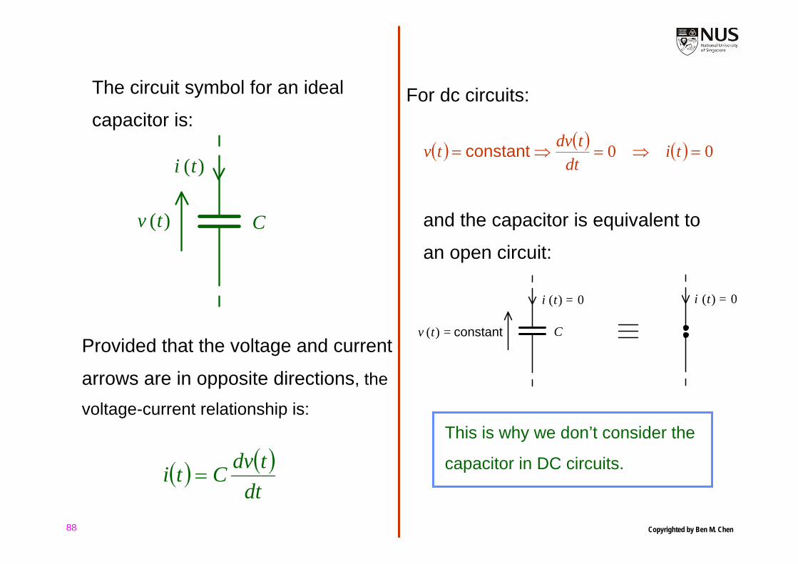
The circuit symbol for an ideal
capacitor is:
Cv (t)
i (t)
Provided that the voltage and current
arrows are in opposite directions, the
voltage-current relationship is:
( ) ( )dt
tdvCti =
For dc circuits:
( ) ( ) ( ) 00 =⇒=⇒= tidt
tdvtv constant
and the capacitor is equivalent to
an open circuit:
Cv (t) = constant
i (t) = 0 i (t) = 0
This is why we don’t consider the
capacitor in DC circuits.
Copyrighted by Ben M. Chen88

Consider the change in voltage,
current and power supplied to the
capacitor as indicated below:
0 t
v( t)
1
vf
0 t
i ( t)
1
vfC
0 t
v ( t)
1
i ( t)p( t) =
vfC 2Area = Energy stored =
vfC 2
2
= Instantaneous power supplied
In general, the total energy stored in
the electric field established by the
charges on the capacitor plates at
time is( ) ( )
2
2 tCvte =
Proof.
[ ]
.0)(if,2
)(
)()(2
)(2
)()(
)()(
)()()()(
2
22
2
=−∞=
−∞−=
=∫=
∫=
∫=∫=
∞−∞−
∞−
∞−∞−
vtCv
vtvC
xvCxdvxvC
dxdx
xdvCxv
dxxixvdxxpte
tt
t
tt
consumed
Copyrighted by Ben M. Chen89

Now consider the operation of a capacitor in an ac circuit:
)cos(2)( vv trtv θω +=)
2cos(2
)sin(2)()(
πθωω
θωω
++=
+−==
vv
vv
tCr
tCrdt
tdvCti
CjIV
ω1
= V
I
Cωj1
With phasor representation, the capacitor behaves as if it is a resistor
with a "complex resistance" or an impedance of
CjZC ω
1= [ ] [ ] 0ReReRe
2
=⎥⎥⎦
⎤
⎢⎢⎣
⎡=== ∗∗
CjI
IZIVIp Cav ω
In phasor format:
Ce= rvθ vjV
=I rvCωπ2e θ vj e
j= rvCω e θ vjj = Cωj V
An ideal capacitor is a non-dissipative but energy-storing device.Copyrighted by Ben M. Chen90

Since the phase of I relative to V that of is
[ ] [ ] [ ] 090Arg1ArgArgArgArg ==⎥⎦
⎤⎢⎣
⎡=⎥⎦
⎤⎢⎣⎡=− Cj
ZVIVI
Cω
the ac current i(t) of the capacitor leads the voltage v(t) by 90°.
a−
)sin( tω
)cos( tω
)sin( tω−
2π−
( ) ⎟⎠⎞
⎜⎝⎛ +==⎟
⎠⎞
⎜⎝⎛ −−
2sincos
2sin πωωπω ttt
Copyrighted by Ben M. Chen91

Example: Consider the following ac circuit:
30319
230 V50 Hz
μFΩ
In phasor notation (taking the source
to have a reference phase of 0):
30
110-6j 2π(50)
= 10j−(319)
30
230j10
=10j−
230
30 −7.3e j 0.32
230 e j 0 = 230
Copyrighted by Ben M. Chen92

Total circuit impedance ( ) Ω−= 1030 jZ
Total circuit reactance [ ] [ ] Ω−=−== 101030ImIm jZX
Total circuit resistance [ ] [ ] Ω=−== 301030ReRe jZR
Current (rms) A3.7=I
Current (peak) A1023.72 ==I
Source V-I phase relationship rad32.0by leadsI
Power factor of entire circuit ( ) leading95.032.0cos =
Power supplied by source ( ) ( )[ ] ( )( ) ( ) kW6.132.0cos3.72303.7230Re 32.0 ==∗ je
Power consumed by resistor ( ) ( ) ( ) kW6.1303.73.7303.7Re 232.032.0 ==⎥⎦⎤
⎢⎣⎡ ×
∗ jj ee
Copyrighted by Ben M. Chen93

Impedance, Resistance, Reactance,
Admittance, Conductance, and SusceptanceRelations?
jXRZ +=Impedance:
Admittance: ( )( )
jBGXR
XjXR
RXRjXR
jXRjXRjXR
jXRZY
+=+
−+
+=
+−
=
−+−
=+
==
222222
11
Conductance SusceptanceCopyrighted by Ben M. Chen94
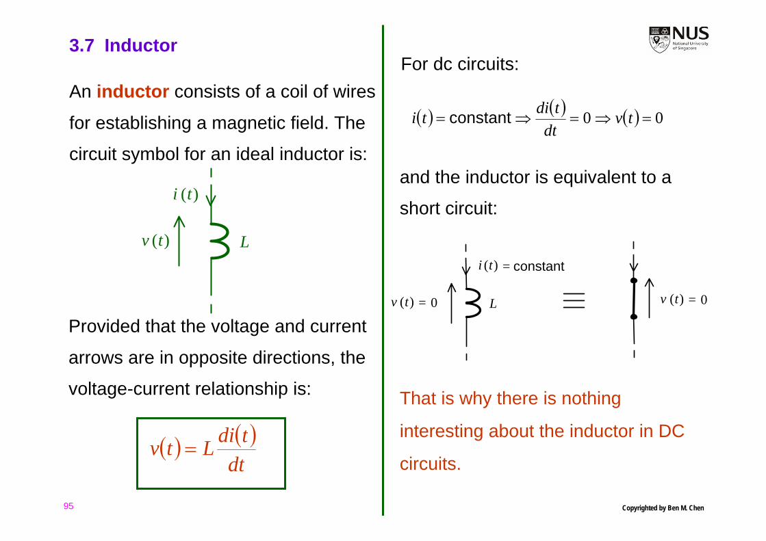
3.7 Inductor
An inductor consists of a coil of wires
for establishing a magnetic field. The
circuit symbol for an ideal inductor is:
Lv (t)
i (t)
Provided that the voltage and current
arrows are in opposite directions, the
voltage-current relationship is:
( ) ( )dt
tdiLtv =
For dc circuits:
( ) ( ) ( ) 00 =⇒=⇒= tvdt
tditi constant
and the inductor is equivalent to a
short circuit:
L= 0v (t)
i = constant(t)
= 0v (t)
That is why there is nothing
interesting about the inductor in DC
circuits.
Copyrighted by Ben M. Chen95

Consider the change in voltage,
current and power supplied to the
inductor as indicated below:
0 t
v( t)
1
i f
0 t
i ( t)
1
i fL
0 t
v ( t)
1
i ( t)p( t) =
i fL 2Area = Energy stored =
i fL 2
2
= Instantaneous power consumed
In general, the total energy stored
in the magnetic field established
by the current i(t) in the inductor
at time t is given by
( ) ( )2
2 tLite =
[ ]
.0)(if,2
)(
)()(2
)(2
)()(
)()(
)()()()(
2
22
2
=−∞=
−∞−=
=∫=
∫=
∫=∫=
∞−∞−
∞−
∞−∞−
itLi
itiL
xiLxdixiL
dxdx
xdiLxi
dxxixvdxxpte
tt
t
tt
Copyrighted by Ben M. Chen96

Now consider the operation of an inductor in an ac circuit:
Lv (t)
i (t) )cos(2)( ii trti θω +=
)2
cos(2
)sin(2)()(
πθωω
θωω
++=
+−==
ii
ii
tLr
tLrdt
tdiLtv
In phasor:
Lv (t)
i (t) ijierI θ=
ILjeLrjeeLrV ii ji
jji )(2/ ωωω θπθ ===
LjIVZL ω==V
I
Lωj
ZL is the impedance of the inductor. The ave. power absorbed by the inductor:
[ ] [ ] [ ] [ ] 0ReReReRe 2 ===== ∗∗∗ ILjILIjIZIVIp Lav ωω
Copyrighted by Ben M. Chen97

Since the phase of I relative to that of V is
[ ] [ ] 0901Arg1ArgArgArgArg −=⎥⎦
⎤⎢⎣
⎡=⎥⎦
⎤⎢⎣
⎡=⎥⎦
⎤⎢⎣⎡=−
LjZVIVI
L ω
the ac current i(t) lags the voltage v(t) by 90º.
As an example, consider the following series ac circuit:
319230 V50 Hz
μFΩ
31.9 mH
3
We can use the phasor representation to convert this ac circuit to a ‘DC’
circuit with complex voltage and resistance.
Copyrighted by Ben M. Chen98

230j10
=3 − 77
10-3j 2π(50) =10j−
230 (31.9)
3
10j
10j−230
3
10j
10j+
773
10j230 770j
770j−230
10j−
Total circuitimpedance Ω=+−= 310103 jjZTotal circuit reactance [ ] [ ] Ω=== 03ImIm ZXTotal circuit resistance [ ] [ ] Ω=== 33ReRe ZRCurrent (rms) A77=ICurrent (peak) A1082772 ==ISource voltage-currentphase relationship ( )phase in0Power factor of entirecircuit ( ) 10cos =
Power supplied bysource ( ) ( )[ ] kW1823077Re =∗
Power consumed byresistor ( ) ( )[ ] kW1877377Re =×∗
Summary of the circuit:
Copyrighted by Ben M. Chen99

Note that the rms voltages across the inductor and capacitor are larger
than the source voltage. This is possible in ac circuits because the
reactances of capacitors and inductors, and so the voltages developed
across them, may cancel out one another:
230
Source=voltage
770
Voltageacross
capacitorj−
+230
Voltageacrossresistor +
770
Voltageacross
inductorj
In dc circuits, it is not possible for a passive resistor (with positive
resistance) to cancel out the effect of another passive resistor (with
positive resistance).
Copyrighted by Ben M. Chen100

3.8 Power Factor Improvement
Consider the following system:
Electrical Machine
230230 V2.3 kW
0.4 lagging power factor
50 Hz
Mains V =
I0
The current I0 can be found as follows:
( )( ) ( )( )25
4.023023004.0
AV230W2300
00
==⇒= II
[ ] [ ]{ }[ ] [ ] [ ] ( ) 16.14.0cosArg
0ArgArg4.0ArgArgcos 1
00
0 −=−=⇒⎭⎬⎫
<−=− −I
VIVI
Due to the small power
factor, the machine
cannot be connected to
standard 13A outlets even
though it consumes only
2.3 kW of power.
Can we improve it?
[ ] 16.1Arg00 250 jIj eeII −==
Copyrighted by Ben M. Chen101

EG1103 Mid-term Test
• When? The time of your tutorial class in the week right after the recess week.
• Where? In your tutorial classroom.• Why? To collect some marks for your final
grade for EG1103.• What? Two questions cover materials up to
DC circuit analysis.
Copyrighted by Ben M. Chen102

To overcome this problem, a parallel capacitor can be used to improve
the power factor:
New Electrical Machine
Mains
e j− 1.1625
OriginalMachine
Zold = 230e j− 1.1625
= e j1.169.2Cj2π1=ZC (50) C
I
230V =
( )23230001023102300025 16.1 −+=−+=+= − CjjCjeZVI j
Cππ
Thus, if we choose mF32.02323000 =⇒= CCπ then A10=I
( ) ( )[ ] 1ArgArgcos =−= VImachinenew offactor Power
and
By changing the power factor, the improved machine can now be connected to
standard 13A outlets. The price to pay is the use of an additional capacitor.
Copyrighted by Ben M. Chen103

To reduce cost, we may wish to use a capacitor which is as small as possible.
To find the smallest capacitor that will satisfy the 13A requirement:
( ) 2222 13237220010 =−+= CI ( )222 23722001013 −+= C
( ) ( ) 22222 3.82372200237220013100 −−=−+−= CC
( ) ( )3.823722003.823722000 +−−−= CC
mF44.0mF2.0 or=C
There are 2 possible values for C, one giving a lagging overall power factor,
the other giving a leading overall power factor. To save cost, C should be
mF2.0=CCopyrighted by Ben M. Chen104

Chapter 4. Frequency Response
Copyrighted by Ben M. Chen105

4.1 RC Circuit
Consider the series RC circuit:
160 mF
Ω2
10-3j2π=
(160) jf f1 1ZC =
2
V
v(t) =a 2cos )+ θ( t2π f
v (t)C
b 2cos )+ φ( t2π f=
= a θe j V = b φe jC
( ) ( )fj
jf
jfZ
Zeab
aebe
VVfH
C
Cjj
jC
211
12
1
2 +=
+=
+==== −θφ
θ
φ
I
FrequencyResponse
)2( CZIV +=Input:CC IZV =Output:
Copyrighted by Ben M. Chen106

The magnitude of H ( f ) is
( )
( ) 22 411
211
ff
ab
VV
VVfH CC
+=
+=
===
and is called the magnitude response.
The phase of H ( f ) is
( )[ ] [ ] [ ]
[ ] ( )ffj
fj
VVVVfH C
C
2tan21Arg
211Arg
ArgArg=ArgArg
1−−=+−=
⎥⎦
⎤⎢⎣
⎡+
=−=
−⎥⎦⎤
⎢⎣⎡=
θφ
and is called the phase response.
The physical significance of these responses is that H ( f )
gives the ratio of output to input phasors, |H ( f )| gives the
ratio of output to input magnitudes, and Arg[H ( f )] gives the
output to input phase difference at a frequency f.
Copyrighted by Ben M. Chen107

Input( ) ( )[ ]752cos23 += ttv π
73 jeV =
( ) ( )[ ] ( ) ⎥⎦⎤
⎢⎣⎡ −==
242cos42sin πππ trtrtv
2
2πjerV −=
Frequency 5=f 4=f
Frequencyresponse ( )
10115j
H+
= ( )81
14j
H+
=
Magnituderesponse ( )
10115 =H ( )
6514 =H
Phaseresponse ( )[ ] ( )10tan5Arg 1−−=H ( )[ ] ( )8tan4Arg 1−−=H
Output( ) ( ) ( )[ ]10tan752cos
10123 1−−+= ttvC π
( )[ ]10tan7 1
1013 −−= j
C eV
( ) ( ) ( )[ ]
( ) ( ) ⎥⎦⎤
⎢⎣⎡ −−=
−=
−
−
28tan42cos
65
8tan42sin65
1
1
ππ
π
tr
trtvC
( )[ ]28tan 1
130π−− −
= jC erV
Copyrighted by Ben M. Chen108

Due to the presence of components such as capacitors and inductors
with frequency-dependent impedances, H ( f ) is usually frequency-
dependent and the characteristics of the circuit is often studied by
finding how H ( f ) changes as f is varied. Numerically, for the series
RC circuit:
f ( ) ( )2411
ffH
+= ( )[ ] ( )ffH 2tanArg 1−−=
0 ( ) dB01log201 == 00=rad0
5.0( )
dB32
1log202
15.041
12
−=⎟⎠⎞
⎜⎝⎛==
+( ) 01 45=rad
45.02tan −−=×− − π
∞→ dB0 ∞−=→ ( ) 01 90rad2
tan −=−=∞− − π
Copyrighted by Ben M. Chen109

0 f0.5
H ( f )
H ( f )[ ]Arg
1 = 0 dB
0.7 =
0f
0.5
90− o
45− o
t
Input
Output
Lowf
t
Output
Input
Highf
− 3 dB
High Frequency
Low Frequency
Copyrighted by Ben M. Chen110

At small f, the output approximates the input. However, at high f, the output
will become attenuated. Thus, the circuit has a low pass characteristic (low
frequency input will be passed, high frequency input will be rejected).
The frequency at which |H ( f )| falls to –3 dB of its maximum value is called
the cutoff frequency. For the above example, the cutoff frequency is 0.5 Hz.
To see why the circuit has a low pass characteristic, note that at low f, C has
large impedance (approximates an open circuit) when compare with R (2 in
the above example). Thus, VC will be approximately equal to V :
=f1ZC VCfLow ∝ ∞ open circuit( ) ≈
R
VV
Copyrighted by Ben M. Chen111

However, at high f, C has small impedance (approximates a short circuit)
when compare with R. Thus, VC will be small:
R
VfHigh VC 0≈ small( )=f
1ZC short circuit( )∝ 0
Key Notes: The capacitor is acting like a short circuit at
high frequencies and an open circuit at low frequencies. It is
totally open for a dc circuit.
Copyrighted by Ben M. Chen112

An Electric Joke
Q: Why does a capacitor block DC but allow AC to pass
through?
A: You see, a capacitor is like this −−−| |−−− , OK. DC
Comes straight, like this −−−−−, and the capacitor stops
it. But AC, goes up, down, up and down and jumps
right over the capacitor!
Copyrighted by Ben M. Chen113

4.2 RL Circuit
Consider the series RL circuit:
Ω5
VLHzf
5V
10-3j 2π =(160) jf fZL =
160 mHHzfv(t)
sinusoidHzf
sinusoid
v (t)L
IInput: V=I ( 5 + ZL ) Output: VL=I ZL
( )jf
jfZ
ZfHVV
L
LL
+=
+==
55 Frequency Response
Copyrighted by Ben M. Chen114

The magnitude response is
( ) 2
2
22
2
255 ff
fffH
+=
+=
The phase response is
( )[ ]
[ ] [ ]
⎟⎠⎞
⎜⎝⎛−=
+−=
⎥⎦
⎤⎢⎣
⎡+
=
−
5tan
2
5ArgArg5
ArgArg
1 fjfjf
jfjffH
π
Numerically:
f ( ) 2
2
25 fffH+
= ( )[ ] ⎟⎠⎞
⎜⎝⎛−= −
5tan
2Arg 1 ffH π
0 ( ) dB0log200 ∞−== 009=rad2π
5 dB32
1log202
1525
52
2−=⎟
⎠⎞
⎜⎝⎛==
+01 45=rad
455tan
2ππ
=⎟⎠⎞
⎜⎝⎛− −
∞→ dB01 =→ ( ) 01 0rad0tan2
==∞− −π
Copyrighted by Ben M. Chen115

Copyrighted by Ben M. Chen116

Copyrighted by Ben M. Chen117

Physically, at small f, L has small impedance (approximates a short circuit)
when compare with R (5 in the above example). Thus, VL will be small:
fLowV
VL 0≈ small( )
R
0fZL∝ ≈ short circuit( )
However, at high f, L has large impedance (approximates an open
circuit) when compare with R. Thus, VL will approximates V :
VL ≈ V
R
VfHigh fZL∝ ≈ (open circuit)∞
Due to these characteristics, the circuit is highpass in nature.Copyrighted by Ben M. Chen118

4.3 Series Tune Circuit
1.4 F
HzfVC
I
V
j 2π =(0.64) jf fZL = 4
= jj2π (1.4)f1 1ZC = f9
0.64 HL =
=C
Ω0.067R =
Hzfv(t)
sinusoidHzf
sinusoid
v (t)C
230
Output
The total impedance is
⎟⎠
⎞⎜⎝
⎛ −+=
++=
++=
ffj
fjfj
ZZRZ CL
914
302
914
302
( )( ) ( )( ) LCCLff
πππ 21
221
61
941
00 ==⇔==Resonance Frequency
Input
RLfQfQ 00 210
30232 π
=⇔===Resistance
atinductorofReactanceQ factor
302
=
Copyrighted by Ben M. Chen119

The frequency response is
( )fjf
fjfj
fjZ
ZVVfH CC
6.03611
914
302
91
2 +−=
++===
The magnitude response is
( )( ) ( ) ( ) ( ) 16.07236
1
6.0361
12222222 +−−
=+−
=ffff
fH
( ) ( )22222
222
726.011
726.01
726.0136236
1
⎟⎟⎠
⎞⎜⎜⎝
⎛−−+⎟⎟
⎠
⎞⎜⎜⎝
⎛−+⎟⎟
⎠
⎞⎜⎜⎝
⎛−−
=
ff
⎟⎟⎠
⎞⎜⎜⎝
⎛−⎟⎟
⎠
⎞⎜⎜⎝
⎛+⎥
⎦
⎤⎢⎣
⎡⎟⎟⎠
⎞⎜⎜⎝
⎛−−
=
726.02
726.0
726.0136
12222
2f
22
2
22
2
22
2
222
⎟⎠⎞
⎜⎝⎛−+⎟
⎠⎞
⎜⎝⎛ −=
+⎟⎠⎞
⎜⎝⎛−
⎟⎠⎞
⎜⎝⎛+⎟
⎠⎞
⎜⎝⎛−=
+−
bcbx
cb
bxbx
cbxx
Since f only appears in the [•]2 term in the denominator and [•]2 >= 0, |H ( f )|
will increase if [•]2 becomes smaller, and vice versa.Copyrighted by Ben M. Chen120

The maximum value for |H ( f )| corresponds to the situation of [•]2 or at a
frequency f = fpeak given by:
0
22
611
726.0136 ffff peakpeakpeak ≈⇔≈⇔≈−=
At f = fpeak , [•]2 and the maximum value for |H ( f )| is
( )( )
( ) QfHfH peakpeak ≈⇔=
⎟⎟⎠
⎞⎜⎜⎝
⎛≈
⎟⎟⎠
⎞⎜⎜⎝
⎛−⎟⎟
⎠
⎞⎜⎜⎝
⎛= 10
2726.01
726.02
726.0
1222
H( f)
f0
QH( f )peak ≈ =10
≈fpeak f0 = 16
The series tuned circuit has a
bandpass characteristic. Low- and
high-frequency inputs will get
attenuated, while inputs close to the
resonant frequency will get amplified
by a factor of approximately Q.
Copyrighted by Ben M. Chen121
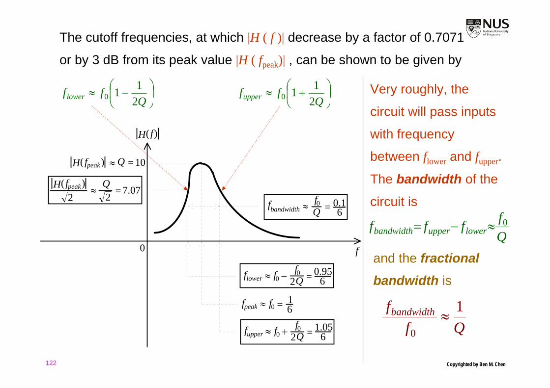
The cutoff frequencies, at which |H ( f )| decrease by a factor of 0.7071
or by 3 dB from its peak value |H ( fpeak)| , can be shown to be given by
⎟⎠
⎞⎜⎝
⎛ −≈Q
fflower 2110 ⎟
⎠
⎞⎜⎝
⎛ +≈Q
ffupper 2110
H( f)
f0
QH( f )peak ≈ = 10
≈fpeak f0 = 16
≈flower f0 = 0.956−
f02Q
≈fupper f0 = 1.056+
f02Q
2H( f )peak ≈ = 7.07Q
2fbandwidth ≈ = 0.1
6f0Q
Very roughly, the
circuit will pass inputs
with frequency
between flower and fupper.
The bandwidth of the
circuit is
Qffff lowerupperbandwidth0≈−=
and the fractional bandwidth is
Qffbandwidth 1
0≈
Copyrighted by Ben M. Chen122

The larger the Q factor, the sharper the magnitude response, the bigger
the amplification, and the narrower the fractional bandwidth:
H( f)
f0
Large Q
Small Q
In practice, a series tune circuit usually consists of a practical inductor or
coil connected in series with a practical capacitor. Since a practical
capacitor usually behaves quite closely to an ideal one but a coil will
have winding resistance, such a circuit can be represented by:
Copyrighted by Ben M. Chen123

Hzf
L
Equivalent circuit for coil or practical inductor
V
R
C VC
The main features are:
Circuit impedancefCj
fLjRZπ
π212 ++=
Resonance frequencyLC
fπ2
10 =
Q factorR
LfQ 02π=
Frequency response ( )
⎟⎟⎠
⎞⎜⎜⎝
⎛+⎟⎟
⎠
⎞⎜⎜⎝
⎛−
=+−
=
0
2
0
22
1
1241
1
ff
Qj
fffCRjLCf
fHππ
Copyrighted by Ben M. Chen124

For the usual situation when Q is large:
Magnitude response Bandpass with ( )fH decreasing as 0→f and ∞→f
Response peak ( )fH peaks at 0fff peak ≈= with ( ) QfH peak ≈
Cutoff frequencies ( )( )
22QfH
fH peak ≈= at
⎟⎠
⎞⎜⎝
⎛ +⎟⎠
⎞⎜⎝
⎛ −≈=Q
fQ
ffff upperlower 211,
211, 00
BandwidthQffff lowerupperbandwidth0≈−=
Fractional bandwidthQf
fbandwidth 10
≈
Copyrighted by Ben M. Chen125

The Q factor is an important parameter of the circuit.
resistance Circuit at reactance Inductor 002 f
RLfQ ==
π
However, since R is usually the winding resistance of the practical coil
making up the tune circuit:
coil practical of ResistanceatcoilpracticalofReactance 0fQ =
As a good practical coil should have low winding resistance and high
inductance, the Q factor is often taken to be a characteristic of the practical
inductor or coil. The higher the Q factor, the higher the quality of the coil.
Copyrighted by Ben M. Chen126

Due to its bandpass characteristic, tune circuits are used in radio and
TV tuners for selecting the frequency channel of interest:
L
C
Channel 5
f5
Channel 8
f8
Amplifierand
OtherCircuits
VCPractical inductor or coil
To tune in to channel 5, C has to
be adjusted to a value of C5 so
that the circuit resonates at a
frequency given by
55 2
1LC
fπ
=f0 f5 f8
H( f)
Copyrighted by Ben M. Chen127

To tune in to channel 8, C has to be adjusted to a value of C8 so that
the circuit resonates at a frequency given by
88 2
1LC
fπ
=
and has a magnitude response of:
f0 f5 f8
H( f)
Copyrighted by Ben M. Chen128

Additional Notes on Frequency Response
Frequency response is defined as the ratio of the phasor of the output
to the phasor of the input. Note that both the input and output could be
voltage and/or current. Thus, frequency response could have
( ) .)()(,
)()(,
)()(,
)( inputVoutputI
inputIoutputI
inputVoutputV
inputIoutputV
Copyrighted by Ben M. Chen129

Chapter 5. Periodic Signals
Copyrighted by Ben M. Chen130

5.1 Superposition
In analyzing ac circuits, we have assumed that the voltages and currents
are sinusoids and have the same frequency f. When this is not the case
but the circuit is linear (consisting of resistors, inductors and capacitors),
the principle of superposition may be used. Consider the following system:
3 2cos )+ 0.1( t4065 2cos )− 0.2( t
i )(t
40.0025 F
The current i(t) can be found by summing the contributions due to the two
sources on their own (with the other sources replaced by their internal
resistances).Copyrighted by Ben M. Chen131

6
I
65 2 cos )− 0.2( t
i )( t
4
1
0.0025 F
e j− 0.25
1j4
1(0.0025) = 100 j−
Copyrighted by Ben M. Chen132

6e j− 0.25100 j−
I 1 =(6)
= e j− 0.256 100 j− e j 1.30.3
65 2 cos )− 0.2( t
i )( t
4
1 = 0.3 2 cos )+ 1.3( t4
0.0025 F
Copyrighted by Ben M. Chen133

I
6
i )( t2
0.0025 F
2 j 401 =(0.0025) 10 j−
3 2 cos )+ 0.1( t40
6 e j 0.13
Copyrighted by Ben M. Chen134

I 2 == 6 10 j− e j 1.10.26
)i ( t2 = 0.26 2 cos )+ 1.1( t40
6 e j 0.1310 j−
e j 0.13− −
−
60.0025 F
3 2 cos )+ 0.1( t40
Copyrighted by Ben M. Chen135

Lastly, the actual current when both sources are present:
3 2cos )+ 0.1( t4065 2cos )− 0.2( t
i )(t
40.0025 F
)i (t2
=0.26 2cos )+1.1( t40−
i )( t1=0.3 2cos )+1.3( t4
+
Copyrighted by Ben M. Chen136

5.2 Circuit Analysis using Fourier Series
Using superposition, the voltages and currents in circuits with sinusoidal
signals at different frequencies can be found.
Circuits with non-sinusoidal but periodic signals can also be analyzed by
first representing these signals as sums of sinusoids or Fourier series.
The following example shows how a periodic square signal can be
represented as a sum of sinusoidal components of different frequencies:
Copyrighted by Ben M. Chen137

t
Original periodic square waveform: v (t)
0 1
Fundamental component: sin(2π t)
t0 1
1
4π
t
Third harmonic: sin(6π t)3
13
Fundamental
sin(2π t)
t
+
third harmonic:+sin(6π t)
3
Any periodic signal can be
represented as an infinite
sum of sine signals.
Freq. is triple.
( ) ( ) ( ) ( )L+++=
510sin
36sin2sin ttttv πππ
Same freq.as the orginal.
Copyrighted by Ben M. Chen138

v )(t
sin(2π t)
sin(6π t)3
160 mF
Ω2
v (t) vC (t)
sin(2π t)
sin(6πt)3
Ω2
160 mF vC (t)
sin(10π t)5
v )(t
Fourierrepresentation
for
2S
f HzSC
160 mF
Ω2s (t)
sC (t)Sinusoid
f Hz
j21(0.16) =πf j f
1
Copyrighted by Ben M. Chen139

( )fj
jf
jfS
SfH C
211
12
1
+=
+==
The frequency response:
From superposition, if the input is the periodic square signal
( ) ( ) ( ) ( )L+++=
510sin
36sin2sin ttttv πππ
then the output will be
( ) ( ) ( ) L+−+−= 4.16sin05.01.12sin44.0 tttvC ππ
( ) ( )[ ]( ) ( )
( ) ( )[ ]( ) ( )
L+×+
×−+
×+
×−=
−−
2
1
2
1
321332tan32sin
121112tan12sin tt ππ
( )[ ]( )
∑+
−=
∞
=
−
L,5,3,1 2
1
212tan2sin
n nnntnπ
Side Notes:
Superposition for
infinite series will
not be examined.
Topic on Fourier
Representation of
periodic signal is
skipped and
hence ...
Copyrighted by Ben M. Chen140

Chapter 6. Transient Circuit Analysis
Copyrighted by Ben M. Chen141

C.3 Linear Differential Equation
General solution:
n th order lineardifferential equation
( ) ( ) ( ) ( )tutxadt
txdadt
txdn
n
nn
n
=+++ −
−
− 01
1
1 L
General solution ( ) ( ) ( )txtxtx trss +=
Steady state responsewith no arbitrary constant
( )( )tu
txss
as form same the have to solutionassuming from obtained integral particular=
Transient response withn arbitrary constants
( )( ) ( ) ( ) 001
1
1 =+++
=
−
−
− txadt
txdadt
txd
tx
trntr
n
nntr
ntr
L
equation shomogeneou of solution general
Copyrighted by Ben M. Chen142

General solution of homogeneous equation:
n th order linearhomogeneous equation
( ) ( ) ( ) 001
1
1 =+++ −
−
− txadt
txdadt
txdtrn
trn
nntr
n
L
Roots of polynomialfrom homogeneousequation
( ) ( ) 0
111
1 ,,
azazzzzz
zzn
nn
n
n
+++=−− −− LL
L
by given :Roots
General solution(distinct roots)
( ) tzn
tztr
nekektx ++= L11
General solution(non-distinct roots)
( ) ( ) ( ) tttttr ekeketkketktkktx 41
731
622
54132
321 ++++++=if roots are 13 13 13 22 22 31 41, , , , , ,
Copyrighted by Ben M. Chen143

Particular integral:
( )txss Any specific solution (with no arbitrary constant)of
( ) ( ) ( ) ( )tutxadt
txdadt
txdn
n
nn
n
=+++ −
−
− 01
1
1 L
Method to determine( )txss
Trial and error approach: assume ( )txss to havethe same form as ( )tu and substitute intodifferential equation
Example to find ( )txss for( ) ( ) tetx
dttdx 32 =+
Try a solution of he t3
( ) ( ) 2.0232 3333 =⇒=+⇒=+ heheheetxdt
tdx tttt
( ) tss etx 32.0=
Standard trial solutions ( ) ( )
( )( ) ( ) ( ) ( )ththtbta
ethhtehtthee
txtu
tt
ttss
ωωωω
αα
αα
sincossincos 21
21
+++
for solution trial
Copyrighted by Ben M. Chen144

6.1 Steady State and Transient Analyses
So far, we have discussed the DC and AC circuit analyses. DC analysis can be
regarded as a special case of AC analysis when the signals have frequency f = 0.
Using Fourier series, the situation of having periodic signals can be handled using
AC analysis and superposition. These analyses are often called steady state
analyses, as the signals are assumed to exist at all time.
In order for the results obtained from these analyses to be valid, it is necessary for
the circuit to have been working for a considerable period of time. This will ensure
that all the transients caused by, say, the switching on of the sources have died
out, the circuit is working in the steady state, and all the voltages and currents are
as if they exist from all time.
However, when the circuit is first switched on, the circuit will not be in the steady
state and it will be necessary to go back to first principle to determine the
behavior of the system.
Copyrighted by Ben M. Chen145

6.2 RL Circuit and Governing Differential Equation
Consider determining i(t) in the following series RL circuit:
3 V 7 H
Ω5t = 0
v(t)
i (t)
where the switch is open for t < 0 and is closed for t ≥ 0.
Since i(t) and v(t) will not be equal to constants or sinusoids for all time,
these cannot be represented as constants or phasors. Instead, the
basic general voltage-current relationships for the resistor and inductor
have to be used:
Copyrighted by Ben M. Chen146

3 7
5t = 0i (t)
v(t) = 7 d i(t)d t
i (t)5
3 7
5
t < 0
i (t) = 0
v(t) = 7 d i(t)d t
i (t)5
3 7
5i (t) = 0
v(t) = 7 d i(t)d t = 0
i (t)5 = 03
voltage crossover the switch
KVL
For t < 0
Copyrighted by Ben M. Chen147

3 7
5i (t)
v(t) = 7 d i(t)d t
i (t)5
t 0≥
0
Applying KVL:
( ) ( ) 0,357 ≥=+ ttidt
tdi
and i(t) can be found from determining the
general solution to this first order linear
differential equation (d.e.) which governs
the behavior of the circuit for t ≥ 0.
Mathematically, the above d.e. is often
written as
( ) ( ) ( ) 0,57 ≥=+ ttutidt
tdi
where the r.h.s. is ( ) 0,3 ≥= ttuand corresponds to the dc source or
excitation in this example.
Copyrighted by Ben M. Chen148

6.3 Steady State Response
Since the r.h.s. of the governing d.e.
( ) ( ) ( ) 0,357 ≥==+ ttutidt
tdi
Let us try a steady state solution of
( ) 0, ≥= tktiss
which has the same form as u(t), as a possible solution.
( ) ( )
( ) ( )
53
3507
357
=⇒
=+⇒
=+
k
k
tidt
tdiss
ss
( ) 0,53
≥= ttiss
( ) ( ) 0,3535
53757 ≥=⎟
⎠⎞
⎜⎝⎛+⎟
⎠⎞
⎜⎝⎛=+ t
dtdti
dttdi
ssss
and is a solution of the governing d.e.
In mathematics, the above solution is
called the particular integral or solution
and is found from letting the answer to
have the same form as u(t). The word
"particular" is used as the solution is only
one possible function that satisfy the d.e.
Copyrighted by Ben M. Chen149

In circuit analysis, the derivation of iss(t) by letting the answer to have
the same form as u(t) can be shown to give the steady state response
of the circuit as t → ∞.
3 7
5
v(t) = 7 d i(t)d t
t → ∞
i (t) = k
v(t) = 7 d i(t)d t = 03 7
5i (t) = k
i (t)5 = k5
Using KVL, the steady state
response is
( ) ∞→=⇒
=⇒
=++=
tti
k
kk
,53
53
50503
This is the same as iss(t).
Copyrighted by Ben M. Chen150

6.4 Transient Response
To determine i(t) for all t, it is necessary to find the complete solution of
the governing d.e.( ) ( ) ( ) 0,357 ≥==+ ttuti
dttdi
From mathematics, the complete solution can be obtained from summing
a particular solution, say, iss(t), with itr(t): ( ) ( ) ( ) 0, ≥+= ttititi trss
where itr(t) is the general solution of the homogeneous equation
( ) ( ) 0,057 ≥=+ ttidt
tdi
( ) ( )( )
5757
57
01 +=+=
+
zzz
tidt
tdiz
dttditr
tr
tr by replaced
75
1 −=z
( ) 0,75
111 ≥==
−tekekti
ttztr
where k1 is a constant (unknown now).
( ) ∞→→=−
tektit
tr ,075
1
Thus, it is called transient response.Copyrighted by Ben M. Chen151

6.5 Complete Response
To see that summing iss(t) and itr(t) gives the general solution of the governing d.e.
( ) ( ) 0,357 ≥=+ ttidt
tdi
note that
( ) 0,53
≥= ttiss 0,3535
537 ≥=⎟
⎠⎞
⎜⎝⎛+⎟
⎠⎞
⎜⎝⎛ t
dtdsatisfies
( ) 0,75
1 ≥=−
tektit
tr satisfies 0,057 75
175
1 ≥=⎟⎟⎠
⎞⎜⎜⎝
⎛+⎟
⎟⎠
⎞⎜⎜⎝
⎛ −−tekek
dtd tt
( ) ( ) 0,53 7
5
1 ≥+=+−
tektitit
trss 3535
537 7
5
175
1 =⎟⎟⎠
⎞⎜⎜⎝
⎛++⎟
⎟⎠
⎞⎜⎜⎝
⎛+
−− ttekek
dtdsatisfies
( ) ( ) ( ) 0,53 7
5
1 ≥+=+=−
tektititit
trss is the general solution of the d.e.
Copyrighted by Ben M. Chen152

i )( tss
t < 0 t 0≥
53
0
Switchclose
t = 0
0
t = 57 (Time constant)
0Complete response
i )( ttri )( tss +
53
+ 53
k1
ek1
e− 57 t t 0≥,k1)( t =i tr
k1
Transient Response
Steady State Response
Complete Response
k1 is to be determined later
Copyrighted by Ben M. Chen153

Note that the time it takes for the transient or zero-input
response itr(t) to decay to 1/e of its initial value is
Time taken for itr(t) to decay to 1/e of initial value
and is called the time constant of the response or system.
We can take the transient response to have died out after a
few time constants.
57
=
Copyrighted by Ben M. Chen154

6.6 Current Continuity for
Inductor
To determine the constant k1 in
the transient response of the RL
circuit, the concept of current
continuity for an inductor has
to be used.
Consider the following example:
i )( tL
0 1 2 4 t
1
2
= 7d
d ti )( tLv )( tL
t
7
7−
To ∞
t
7
i )( tL v )( tL =Instantaneous power supplied
To ∞
14−
Lv (t)
i (t)
= 7
Copyrighted by Ben M. Chen155

Due to the step change or discontinuity in iL(t) at t = 2,
and the power supplied to the inductor at t = 2 will go
to infinity. Since it is impossible for any system to
deliver an infinite amount of power at any time, it is
impossible for iL(t) to change in the manner shown.
In general, the current through an inductor must be
a continuous function of time and cannot change in a
step manner.
Copyrighted by Ben M. Chen156

3 V 7 H
Ω5t = 0
v(t)
i )( t
Now back to our RL Circuit:
0
53
+ 53
Switchclose
+ 53
e− 57 t t 0≥,
i )( t =
= 53 +
t < 0,i )( t = 0
k1
i )( ttri )( tss +
k1
Using current continuity for an
inductor at t = 0:
( )530
530 11 −=⇒=+== kkti
( )⎪⎩
⎪⎨⎧
≥−
<= −
0,53
53
0,0
75
te
tti t
0
53
Switchclose
i )( t =
= 53 −
t < 0,i )( t = 0
53
i )( ttri )( tss +
e− 57 t t 0≥,
Copyrighted by Ben M. Chen157

6.7 RC Circuit
Consider finding v(t) in the following
RC circuit:
3 V7 F
Ω5
v(t)2 V
Ω500
t = 0
i (t)
where the switch is in the
position shown for t < 0 and is
in the other position for t ≥ 0.
37
5
v(t)2
500
d v(t)d t= 7i (t)
t < 0
Taking the switch to be in this
position starting from t = −∞, the
voltages and currents will have
settled down to constant values
for practically all t < 0.
( ) ( ) ( ) 0,077 <=== tdt
ddt
tdvti constant
Copyrighted by Ben M. Chen158

37
5
2
500
dv (t)d t= 7i (t)
t < 0
v(t)
= 0
37
5
2
500
i (t)
=500 i (t) 0
v(t) = − 2
= 0
t 0≥
37
5
2
500
d v (t)d t= 7i (t)
v(t)
5i (t) dd t= 35v(t)
Applying KVL:
( ) ( ) ( ) 0,335 ≥==+ ttutvdt
tdv
( ) ( ) ( ) 0, ≥+= ttvtvtv trss
which has a solution
Copyrighted by Ben M. Chen159
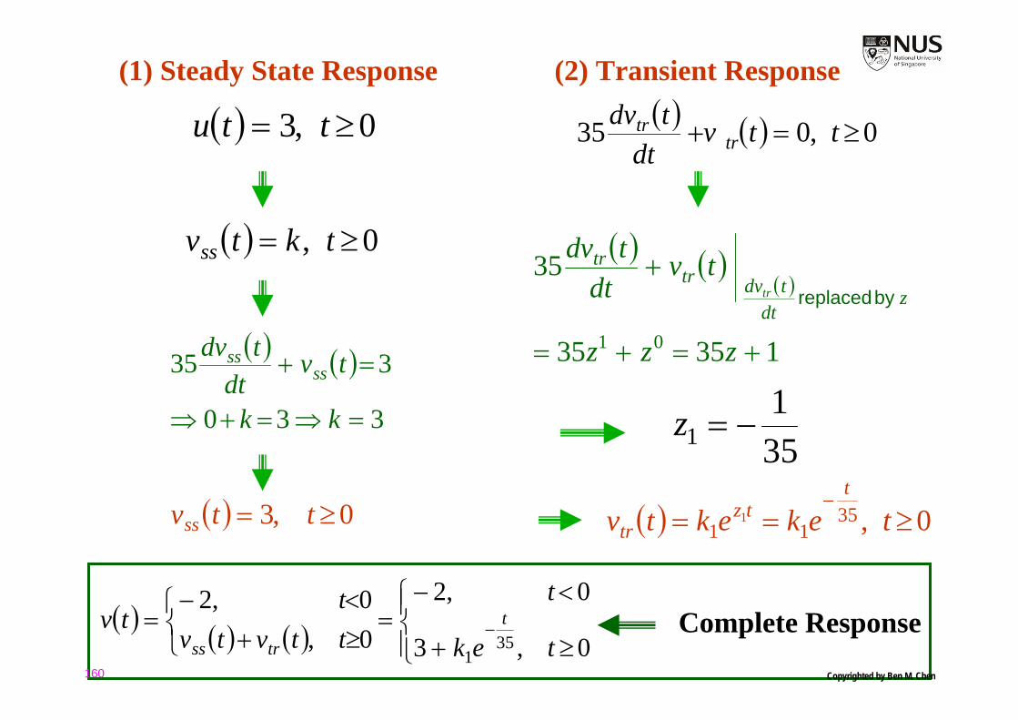
(1) Steady State Response
( ) 0,3 ≥= ttu
( ) ( )
330
335
=⇒=+⇒
=+
kk
tvdt
tdvss
ss
( ) 0, ≥= tktvss
( ) 0,3 ≥= ttvss
(2) Transient Response( ) ( ) 0,035 ≥=+ ttv
dttdv
trtr
( ) ( )( )
13535
35
01 +=+=
+
zzz
tvdt
tdvz
dttdvtr
tr
tr by replaced
351
1 −=z
( ) 0,3511
1 ≥==−
tekektvt
tztr
( ) ( ) ( ) ⎪⎩
⎪⎨⎧
≥+
<−=
⎩⎨⎧
≥+<−
= −0,3
0,2
0,0,2
351 tek
t
ttvtvt
tv t
trssComplete Response
Copyrighted by Ben M. Chen160

6.8 Voltage Continuity for Capacitor
To determine k1 in the transient response of the RC circuit, the concept
of voltage continuity for a capacitor has to be used.
Similar to current continuity for an inductor, the voltage v(t) across a
capacitor C must be continuous and cannot change in a step manner.
Thus, for the RC circuit we consider, the complete solution was derived as:
( ) ( ) ( ) ⎪⎩
⎪⎨⎧
≥+
<−=
⎩⎨⎧
≥+<−
= −0,3
0,2
0,0,2
351 tek
t
ttvtvt
tv t
trss
At t = 0,
( ) 5230 11 −=⇒−=+= kkv ( )⎪⎩
⎪⎨⎧
≥−
<−= −
0,53
0,2
35 te
ttv t
Copyrighted by Ben M. Chen161

6.9 Transient with Sinusoidal Source
Consider the RL circuit with the dc source changed to a sinusoidal one:
7
5t = 0i (t)
3 2cos )+ 0.1( tω
For t < 0 when the switch is open:
7
5
t < 0
i (t) = 0
7 d i(t)d t = 03 2cos )+ 0.1( tω
Copyrighted by Ben M. Chen162
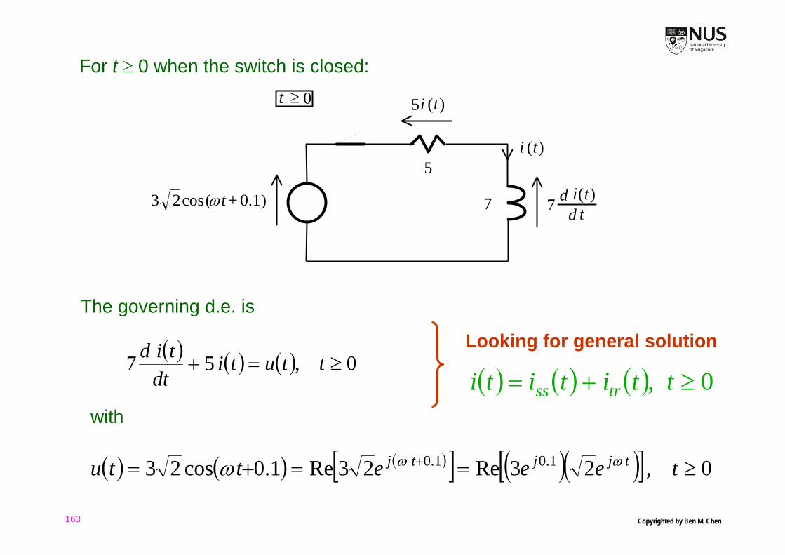
For t ≥ 0 when the switch is closed:
7
5i (t)
7 d i(t)d t
i (t)5t 0≥
3 2cos )+ 0.1( tω
The governing d.e. is
( ) ( ) ( ) 0,57 ≥=+ ttutidt
tid
( ) ( ) ( )[ ] ( )( )[ ] 0,23Re23Re1.0cos23 1.01.0 ≥==+= + teeettu tjjtj ωωω
with
Looking for general solution
( ) ( ) ( ) 0, ≥+= ttititi trss
Copyrighted by Ben M. Chen163

Since u(t) is sinusoidal in nature, a trial solution for the steady state
response or particular integral iss(t) may be
( ) ( ) ( ) ( )[ ] 0,2Recos2 ≥=+= teretrti tjjss
ωθθω
( ) ( ) ( )( )[ ] ( )( )[ ]tjjtjj
ssss ere
dteredti
dttdi ωθ
ωθ2Re52Re757 +=+
( )( )( )[ ] ( )( )[ ]tjjtjj ereejre ωθωθ ω 2Re52Re7 +=
( )( )( )[ ]tjj ejre ωθ ω 257Re +=
( )( )[ ] )(23Re 1.0 tuee tjj == ω
( ) 1.0357 jj erej =+ θωThis is Method One:
Copyrighted by Ben M. Chen164

Method Two:
7
5i (t)
v(t) = 7 d i(t)d t
i (t)5t 0≥
3 2cos )+ 0.1( tω
3 j 0.1e
I
ωj 7
5
5
ωj 7I
=I r e θj
=+ωj 7 5( )I +ωj 7 5( )r e θj = 3 j 0.1eCopyrighted by Ben M. Chen165

( ) 1.0357 jj erej =+ θω
(1) Steady State Response
753 1.0
ωθ
jere
jj
+=⇒
222
1.0
753
753
ωω +=
+=
je
rj
[ ] [ ]
⎟⎠⎞
⎜⎝⎛−=
+−=
−
57tan1.0
75ArgArg
1
1.0
ωωθ je j
(2) Transient Response
( ) ( ) 0,057 ≥=+ ttidt
tditr
tr
itr(t) will have the same form as the dc
source case:
( ) 0,75
1 ≥=−
tektit
tr
( ) ( ) 0,5
7tan1.0cos492523cos2 1
2≥⎥⎦
⎤⎢⎣⎡
⎟⎠⎞
⎜⎝⎛−+
+=+= − tttrtiss
ωωω
θω
Complete Response
Copyrighted by Ben M. Chen166

Complete Response
( ) ( ) ( ) 0, ≥+= ttititi trss
0,5
7tan1.0cos492523 7
5
11
2≥+⎥⎦
⎤⎢⎣⎡
⎟⎠⎞
⎜⎝⎛−+
+=
−− tekttωω
ω
To determine k1, the continuity of i(t), the current through the inductor, can be used.
( ) 0,0 <= tti ( ) ( ) ( ) 11
2 57tan1.0cos
492523000 kiii trss +⎥⎦
⎤⎢⎣⎡
⎟⎠⎞
⎜⎝⎛−
+=+= − ω
ω
⎥⎦⎤
⎢⎣⎡
⎟⎠⎞
⎜⎝⎛−
+−= −
57tan1.0cos
492523 1
21ω
ωk
⎪⎩
⎪⎨
⎧
≥⎪⎭
⎪⎬⎫
⎪⎩
⎪⎨⎧
⎥⎦⎤
⎢⎣⎡
⎟⎠⎞
⎜⎝⎛−−⎥⎦
⎤⎢⎣⎡
⎟⎠⎞
⎜⎝⎛−+
+
<
= −−− 0,5
7tan1.0cos5
7tan1.0cos492523
0,0)( 7
511
2tet
tti tωωω
ω
Copyrighted by Ben M. Chen167

An FAQ: Can we apply KVL to the rms values of voltages in AC circuits?
Answer: No. In an AC circuit, KVL is valid for the phasors of the voltages
in a closed-loop, i.e., the sum of the phasors of voltages in a closed-loop is
equal to 0 provided that they are all assigned to the same direction. KVL
cannot be applied to the magnitudes or rms values of the voltages alone.
For example, a closed-loop circuit containing a series of an AC source, a
resistor and a capacitor could have the following situation: The source has
a voltage with a rms value of 20V, while the resistor and the capacitor have
their voltages with the rms values of 9V and 15V, respectively. All in all, if
you want to apply KVL in AC circuits, apply it to the phasors of its voltages.
By the way, KVL is valid as well when the voltages are specified as functions
of time. This is true for any type of circuits.
Copyrighted by Ben M. Chen168

6.10 Second Order RLC Circuit
Consider determining v(t) in the following series RLC circuit:
11 V7 F v(t)
i (t)
2 V
Ω500
t = 0
3 5 HΩ
t = 0
Both switches are in the position shown for t < 0 & are in the other positions for t ≥ 0.
117 v(t)
2
5003 5
dv (t)d t7
i (t) = 0For t < 0
Copyrighted by Ben M. Chen169

Taking the switches to be in the positions shown starting from t = − ∞, the
voltages and currents will have settled down to constant values for
practically all t < 0 and the important voltages and currents are given by:
dv (t)d t7 = 0
v(t) = 211
72
5003 5
0
Mathematically:
( ) 0,2 <= ttv & ( ) 0,0 <= tti
Copyrighted by Ben M. Chen170

dv (t)d t7
117 v(t)
2
5003 5
d v (t)d t35 2
2dv (t)d t21For t ≥ 0
2
2 )()()(dt
tvdLCdt
tdvCdtdL
dtdiLtvL =⎟
⎠⎞
⎜⎝⎛==
Applying KVL:( ) ( ) ( ) ( ) 0,112135 2
2≥==++ ttutv
dttdv
dttvd
Due to the presence of 2 energy storage elements, the governing d.e. is a
second order one and the general solution is
( ) ( ) ( ) 0, ≥+= ttvtvtv trss
Copyrighted by Ben M. Chen171

(1) Steady State Response
( ) 0,11 ≥= ttu ( ) 0, ≥= tktvss
( ) ( ) ( ) 11002135 2
2=++=++ ktv
dttdv
dttvd
ssssss ( ) 0,11 ≥= ttvss
(2) Transient Response
( ) ( ) ( )( )
1213521352135 20122
2++=++=++ zzzzztv
dttdv
dttvd
zdt
tdvtr
trtr
tr by replaced
( ) ( ) ( ) 0,02135 2
2≥=++ ttv
dttdv
dttvd
trtrtr
( ) 0,06.02
54.0121
21 ≥+=+= −− tekekekektv tttztztr
( )( )( ) ( ) 06.0,54.0
3521721
35213542121,
2
21 −−=±−
=−±−
=zz
Copyrighted by Ben M. Chen172
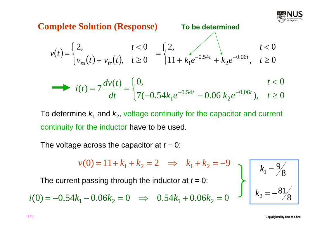
Complete Solution (Response)
( ) ( ) ( ) ⎩⎨⎧
≥++<
=⎩⎨⎧
≥+<
= −− 0,110,2
0,0,2
06.02
54.01 tekek
tttvtvt
tv tttrss
To be determined
To determine k1 and k2, voltage continuity for the capacitor and current
continuity for the inductor have to be used.
The voltage across the capacitor at t = 0:
9211)0( 2121 −=+⇒=++= kkkkv
⎩⎨⎧
≥−−<
== −− 0),06.054.0(70,0)(7)( 06.0
254.0
1 tekekt
dttdvti tt
The current passing through the inductor at t = 0:
006.054.0006.054.0)0( 2121 =+⇒=−−= kkkki
89
1 =k
881
2 −=k
Copyrighted by Ben M. Chen173

General RLC Circuit:
7
5003 5
t 0≥
)( tvtr
0
dd t35 2
2 )( tvtrdd t21 )( tvtr
R L
C
dttdvCti tr )()( =
RC LC
By KVL: ( ) ( ) ( ) 0,02
2≥=++ ttv
dttdvRC
dttvdLC tr
trtr
for t ≥ 0
( ) ( ) ( )( )
01122
2=++=++ RCzLCztv
dttdvRC
dttvdLC
zdt
tdvtr
trtr
tr by replaced
LCLCRCRCzz
24)(,
2
21−±−
=Copyrighted by Ben M. Chen174
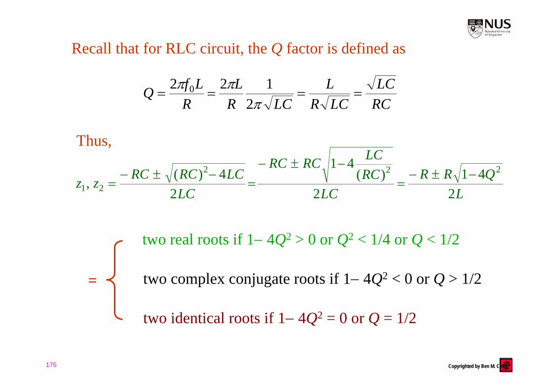
Recall that for RLC circuit, the Q factor is defined as
RCLC
LCRL
LCRL
RLfQ ====
πππ
2122 0
LQRR
LCRCLCRCRC
LCLCRCRCzz
241
2)(
41
24)(,
222
21−±−
=−±−
=−±−
=
Thus,
=
two real roots if 1− 4Q2 > 0 or Q2 < 1/4 or Q < 1/2
two identical roots if 1− 4Q2 = 0 or Q = 1/2
two complex conjugate roots if 1− 4Q2 < 0 or Q > 1/2
Copyrighted by Ben M. Chen175

6.11 Overdamped Response
Reconsider the previous RLC example, i.e.,
72
5003 5
t 0≥
)( tvtr
0
dd t35 2
2 )( tvtrdd t21 )( tvtr
( ) ( ) ( ) 0,02135 2
2≥=++ ttv
dttdv
dttvd
trtrtr
212817.0
2135
<===RCLCQ
( )( )( ) ( ) 06.0,54.0
3521721
35213542121,
2
21 −−=±−
=−±−
=zz
Copyrighted by Ben M. Chen176

( ) 0,06.02
54.0121
21 ≥+=+= −− tekekekektv tttztztr
k1
− t t 0≥,ek20.06
0 t
k2
− t t 0≥,ek10.54
0 t
0 t
k1 k2+)( t =vtr
− tek10.06 − t t 0≥,ek2
0.54+
Due to its exponentially decaying
nature, the response itr(t) and the RLC
circuit are said to be overdamped.
Typically, when an external input is
suddenly applied to an overdamped
system, the system will take a long time
to move in an exponentially decaying
manner to the steady state position.
The response is slow and sluggish, and
the Q factor is small.
Copyrighted by Ben M. Chen177

6.12 Underdamped Response
72
5000.03 5
t 0≥
)( tvtr
0
dd t35 2
2 )( tvtrdd t0.21 )( tvtr
2128
703.05
>==Q ( ) ( ) ( ) 0,021.035 2
2≥=++ ttv
dttdv
dttvd
trtrtr
( )( )( ) ( ) 17.0003.0
35296.13921.0
352135421.021.0,
2
21 jzz ±−=−±−
=−±−
=
2)0( =trv
Copyrighted by Ben M. Chen178

( ) tztztr ekektv 21
21 += ( ) ( ) tjtj ekek 17.0003.02
17.0003.01
−−+− +=
( ) ( ) tjtjtr ejkejkti 17.0003.0
217.0003.0
1 )17.0003.0(7)17.0003.0(7)( −−+− −−++−=
( )
0)(19.1042.0
)(19.1)(021.0
)17.0003.0(7)17.0003.0(70
21
2121
21
=−+−=
−++−=
−−++−=
kkj
kkjkk
jkjkitr
0353.021 jkk −=−
( ) 20 21 =+= kkvtr
Copyrighted by Ben M. Chen179
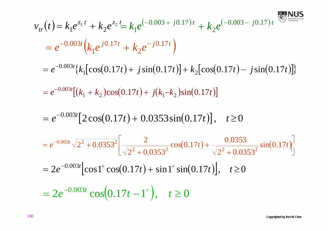
( ) tztztr ekektv 21
21 += ( ) ( ) tjtj ekek 17.0003.02
17.0003.01
−−+− +=
( )tjtjt ekeke 17.02
17.01
003.0 −− +=
( ) ( )[ ] ( ) ( )[ ]{ }tjtktjtke t 17.0sin17.0cos17.0sin17.0cos 21003.0 −++= −
( ) ( ) ( ) ( )[ ]tkkjtkke t 17.0sin17.0cos 2121003.0 −++= −
( ) ( )[ ] 0,17.0sin0353.017.0cos2003.0 ≥+= − ttte t
( ) 0,117.0cos2 003.0 ≥−= − tte t o
( ) ( )⎥⎦⎤
⎢⎣
⎡+
++
+= − tte t 17.0sin0353.02
0353.017.0cos0353.02
20353.022222
22003.0
( ) ( )[ ] 0,17.0sin1sin17.0cos1cos2 003.0 ≥+= − ttte t oo
Copyrighted by Ben M. Chen180

t0
− t t 0≥,e 0.003
Frequency = 0.17
)( t =vtr t 0≥,− te 0.003 cos(0.17t )
22
2 _ 1o
When an external input is applied to an
underdamped system, the system will
oscillate. The oscillation will decay expon-
entially but it may take some time for the
system to reach its steady state position.
Underdamped systems have large Q
factors and are used in systems such as
tune circuit. However, they will be not be
suitable in situations such as car
suspensions or instruments with moving
pointers.
It will take too long for the pointer to
oscillate and settle down to its final position
if the damping system for the pointer is
highly underdamped in nature.
Since this is an exponentially decaying
sinusoid, the response vtr(t) and the RLC
circuit are said to be underdamped.
Copyrighted by Ben M. Chen181

6.13 Critically Damped Response
72
5005
t 0≥
)( tvtr
0
dd t35 2
2 )( tvtrdd t
)( tvtr
207
140
dd t
)( tvtr7
21
77205
==Q
( ) ( ) ( ) 0,014035 2
2≥=++ ttv
dttdv
dttvd
trtrtr
351, 21 −=zz
( ) ( ) ( ) 2)0( 135
21211 ==⇒+=+=
−kvetkketkktv tr
ttz
tr
( ) ( )3520
353570
2
0
35212
0
3521 =⇒=⎟
⎠⎞
⎜⎝⎛ −−=+=
=
−
=
−ketkkketkk
dtdi
t
t
t
ttr
Copyrighted by Ben M. Chen182

Copyrighted by Ben M. Chen183

Example: The switch in the circuit shown in the following
circuit is closed at time t = 0. Obtain the current i2(t) for t > 0.
A 10 Ω B C
t ≥ 0 i2 5 Ω
100 V 0.01 H 5 Ω
i1
F E D
After the switch is closed, the current passing through the source
or the 10Ω resistor is i1 + i2. Applying the KVL to the loops,
ABEFA and ABCDEFA, respectively, we obtain
Copyrighted by Ben M. Chen184

( )( ) 100510
10001.0510
221
1121
=++
=+++
iiidtdiiii
( ) 15/10100 12 ii −=
3333833 11 =+ idt
di
( ) A0.4833/33331 ==∞i 0.4)( 8331 += − teti α
( ) 001 =i 0.4−=α ( )teti 8331 10.4)( −−=
teti 8332 67.20.4)( −+=
Copyrighted by Ben M. Chen185

Chapter 7: Magnetic Circuit
Copyrighted by Ben M. Chen186

7.1 Magnetic Field and Material
In electrostatic, an electric field is formed by static charges. It is described in
terms of the electric field intensity. The permittivity is a measure of how easy
it is for the field to be established in a medium given the same charges.
Similarly, a magnetic field is formed by moving charges or electric currents.
It is described in terms of the magnetic flux density B, which has a unit of
tesla(T) = (N/A)m. The permeability μ is a measure of how easy it is for a
magnetic field to be formed in a material. The higher the μ, the greater the
B for the same currents.
In free space, μ is mH104 70
−×= πμ . The relative permeability μr is
0μμμ =r
Most "non-magnetic" materials such as air and wood have
μr ≈ 1. However, "magnetic materials" such as iron and steel
may have μr ≈ 1000.Copyrighted by Ben M. Chen187

7.2 Magnetic Flux ---- Consider the following magnetic system:
N turns
Magnetic material
i
Permeability μ
Cross sectional area A
Average length l
If μ is large, almost
the entire magnetic
field will be
concentrated inside
the material and
there will be no flux
leakage.The distribution of flux density B or field lines will be
iTotal flux Φ
Field linesform closed paths
N turns
Since the field lines form
closed paths and there
is no leakage, the total
flux Φ passing through
any cross section of the
material is the same.Copyrighted by Ben M. Chen188

Assuming the flux to be uniformly distributed so that the flux density B have
the same value over the entire cross sectional area A:
Total flux Φ
Cross sectional area A
Same flux densityB = ΦA
AB Φ
= with units ( ) ( )2mWbweberTtesla =
Copyrighted by Ben M. Chen189

7.3 Ampere's Law
The values of Φ or B can be calculated using Ampere's law:
Line integral of along any closed path = current enclosed by pathμB
N turns
i
Path length l
Cross sectional area A
Permeability μ
Line integral of along dotted pathμB
Φ⎟⎠
⎞⎜⎝
⎛==AlBl
μμ
= Current enclosed by dotted path NiΦ⎟
⎠
⎞⎜⎝
⎛=AlNi
μ
Copyrighted by Ben M. Chen190

Note that the ratio H = B/μ is called the magnetic field
intensity and Ampere's law is usually stated in terms of
H. Stating the law in terms of H has the advantage that
the effects of magnetic materials, which influence μ, is
not in the main equation. In a certain sense,
characterizes the magnetic field due to only current
distributions. By multiplying H with μ to end up with the
most important flux density B, the effect of the medium is
taken into consideration.
Φ⎟⎠
⎞⎜⎝
⎛=AlNi
μi
lN
AlANi
ABH ⎟
⎠⎞
⎜⎝⎛==
Φ==
μμ
μμ
Copyrighted by Ben M. Chen191

B
H
.current the tolpropotiona is which, iilNH ⎟
⎠⎞
⎜⎝⎛=
μBH =
0
Saturated
Saturated
Copyrighted by Ben M. Chen192

7.4 Magnetic and Electric Circuits --- A more complicated example:
N turns
i
Area A1
Average length l2
Average length l1
Area A2
Permeability μ1
Permeability μ2
N turns
i
Area A2
Total flux Φ
Flux density = ΦB2 A2
Area A1
Total flux Φ
Flux density = ΦB1 A1
Assuming no flux leakage and uniform flux distribution, the field lines, total flux and flux densities are:
Ampere’s Law:Line integral of along any closed path = current
enclosed by path
μB
Copyrighted by Ben M. Chen193

N turns
i
Same total flux ΦArea A1Average length l 1
Permeability μ1 Flux densityB1
Line integral =l 1
μ1
B1 = A1
l1μ1
Φ
Area A2Average length l2
Permeability μ2 Flux densityB2
Line integral =l2
μ2
B2 = A2
l2μ2
Φ
Average length l2 Area A2
Permeability μ2 Flux density B2
Line integral = Φ=22
2
2
22
AlBl
μμ
Φ=22
2
2
22
AlBl
μμ
Average length l1 Area A1
Permeability μ1 Flux density B1
Line integral = Φ=11
1
1
11
AlBl
μμ
Line integral of along entire pathμB Φ⎟⎟
⎠
⎞⎜⎜⎝
⎛+=+=
22
2
11
1
2
22
1
11
Al
AllBlB
μμμμ
= Current enclosed by path = Ni
Φ⎟⎟⎠
⎞⎜⎜⎝
⎛+=
22
2
11
1
Al
AlNi
μμ
Copyrighted by Ben M. Chen194

Note that the above process of calculation magnetic flux is the same
as the calculation of current in the following electric circuit:
Ni
Φ1= A1
l1μ1
2= A2
l2μ2
1Φ 2Φ
Φ
ℜ ℜ
ℜℜ
From KVL, the same equation can be obtained:
Φ⎟⎟⎠
⎞⎜⎜⎝
⎛+=ℜΦ+ℜΦ=
22
2
11
121 A
lA
lNiμμ
This is not surprising because the two basic laws in electric circuits are
equivalent to the two basic laws in magnetic circuits and the following
quantities are equivalent:Copyrighted by Ben M. Chen195

Electric circuits Magnetic circuits
KCL:total current entering a closedsurface equals total currentleaving the surface
Flux lines form closed path:total flux entering a closed surfaceequals total flux leaving the surface
KVL:sum of voltages along a closedpath equals zero
Ampere's law:integral or sum of B μ ("magneticvoltage drops") along a closed pathequals currents enclosed ("magneticvoltage sources")
Voltage Ni (magnetomotive force or mmf)
Current Φ (flux)
Resistance ℜ =lA1
1 1μ (reluctance)
Copyrighted by Ben M. Chen196

Thus, provided there is no flux leakage and uniform distribution of flux across
any cross section, the parallel magnetic circuit with reluctances as indicated:
N turns
i
Φ1 Φ2
2
1
53
4
6 7
ℜ ℜ
ℜℜ
ℜℜ
ℜ
N i
Φ1 Φ22ℜ 4ℜ
7ℜ6ℜ
5ℜ3ℜ
1ℜ
equivalent one to the other
You can use the DC
circuit techniques to
solve this problem.
Copyrighted by Ben M. Chen197

7.5 Inductance --- Consider the magnetic circuit:
N turns
Permeability μ
Area A
Average length l
i )(t
Assuming no flux leakage and uniform flux distribution, the reluctance and
the flux linking or enclosed by the winding is
Al
μ =ℜ ( ) ( )
ℜ==Φ
tNit
reluctancemmfand
Copyrighted by Ben M. Chen198

From Faraday's law of induction, a voltage will be induced in the winding
if the flux linking the winding changes as a function of time. This induced
voltage, called the back emf (electromotive force) will attempt to oppose
the change and is given by
( ) ( ) ( )dt
tdiNdt
tdNtvℜ
=Φ
=
2i )( tN=Φ )( t
Flux linking winding
N turns
i )( t
ℜ
Voltage induced
N=v )( t Φ )( tdd t =
i )( tdd t
N 2
ℜ( ) ( ) ( )
dttdiN
dttdNtv
ℜ=
Φ=
2
=
i (t)
Lv (t) = L dd ti (t) N 2
ℜ
An equivalent inductor:
The inductanceCopyrighted by Ben M. Chen199
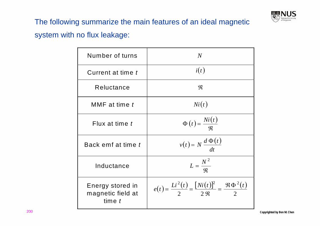
The following summarize the main features of an ideal magnetic
system with no flux leakage:
Number of turns N
Current at time t ( )ti
Reluctance ℜ
MMF at time t ( )tNi
Flux at time t ( ) ( )ℜ
=Φ
tNit
Back emf at time t ( ) ( )dt
tdNtv Φ=
Inductanceℜ
=2NL
Energy stored inmagnetic field at
time t
( ) ( ) ( )[ ] ( )222
222 ttNitLite Φℜ=
ℜ==
Copyrighted by Ben M. Chen200

7.6 Force --- Consider the magnetic relay:
turns
8 cm
7 cm
2 cm2
0.1 cm
Permeabilityμ04000
300
5 A
Air gap permeability μ0
Movable armatureheld stationary
by spring
With no flux leakage and uniform flux distribution (even in air gaps)
Reluctance of entire magnetic material
( )( ) ( ) 0
240
20 8
98.2m1024000
m298.0cm24000
cm1.08cm72μμμ
=×
=−+
= −
( )( ) ( ) 00
20
10cm11.0
cm2cm1.02
μμμ===
Reluctance of two air gaps
Total reluctance000
375.10108
3μμμ
=+=ℜ=
Flux
( )
( ) Wb10182.0104145
375.105300
370
−− ×=×=
=ℜ
=Φ
π
μ mmf
Copyrighted by Ben M. Chen201

Due to the much smaller permeability, the reluctance of the air gaps is much
larger than that of the entire magnetic material. The inductance and energy
stored in the system are
( ) ( ) mH9.10375.10300
0
22
==ℜ
=μ
turns of no.LInductance:
Energy stored in magnetic field =( ) J137.0
210182.0375.10
2 0
232=
×=
Φℜ −
μ
To determine the force of attraction f on the armature, suppose the
armature moves in the direction of f by δl so that the total reluctance
changes by δℜ. Also, suppose the current is changed by δi but the flux is
not changed:
Copyrighted by Ben M. Chen202

turns300
5 + δ i
0.1 cm − δ l
fForce
2 cm2
Same flux Φ as before
As there is no change in flux
linkage (which will be the case if
the magnetic system is close to
saturation), there is no back emf
and there is no energy supplied
by the electrical system. Then
Work done by armature = f (δl)
Increase in energy stored in magnetic field
( )222
222 Φℜ=
Φℜ−
Φℜ+ℜ=
δ δ
From energy conservation:
( )l
flfδ
δ δδ ℜ⎟⎟⎠
⎞⎜⎜⎝
⎛ Φ−=⇒
Φℜ−=
22
22
For our example
( ) ( ) 0
4
20
20
10cm2cm1.0
cm2cm1.02
μδ
μμδ δ ll
−=⎥⎦
⎤⎢⎣
⎡−
−=ℜ
( )( ) N132
104210182.010
210
2 7
234
0
242=
××
=Φ
=ℜ
⎟⎟⎠
⎞⎜⎜⎝
⎛ Φ−= −
−
πμδ δ
lf
Copyrighted by Ben M. Chen203

7.7 Mutual InductorReluctance ℜ
N2N1
Flux Φ (t)
i1(t) i2 (t)
v2 (t)v1(t)
Primarywinding
Secondarywinding
The two dots are
associated with the
directions of the
windings. The fields
produced by the two
windings will be
constructive If the
currents going into
the dots have the
same sign.
Total mmf = ( ) ( )tiNtiN 2211 +
( ) ( ) ( )ℜ+
=ℜ
=Φ=
tiNtiNt 2211mmftotalTotal flux
( ) ( ) ( ) ( )dt
tdiNNdt
tdiNdt
tdNtv 22112
111 ⎟
⎠⎞
⎜⎝⎛
ℜ+⎟⎟
⎠
⎞⎜⎜⎝
⎛ℜ
=Φ
=
( ) ( ) ( ) ( )dt
tdiNdt
tdiNNdt
tdNtv 222121
22 ⎟⎟⎠
⎞⎜⎜⎝
⎛ℜ
+⎟⎠⎞
⎜⎝⎛
ℜ=
Φ=
ℜ
•ℜ
=ℜ
22
2121 NNNN
Copyrighted by Ben M. Chen204

Inductance of primary winding on its own ℜ
==2
11
NL
Inductance of secondary winding on its own ℜ
==2
22
NL
( ) ( ) ( ) ( ) ( )dt
tdiMdt
tdiLdt
tdiLLdt
tdiLtv 211
221
111 +=+=
( ) ( ) ( ) ( ) ( )dt
tdiLdt
tdiMdt
tdiLdt
tdiLLtv 22
122
1212 +=+=
Mi1(t) i2 (t)
=2
ℜ
= Ldd ti1(t)
v2(t) 2+M dd ti2(t)
= L dd ti1(t)
v1(t) 1 + M dd ti2(t) L1 L2
L1N1 , =
2
ℜL2N2 , =M 2 L1 L2 for no flux leakage and perfect coupling
where is called the mutual inductance between the two
windings. Graphically,21LLM =
Copyrighted by Ben M. Chen205

In an ac environment when the currents i1(t) and i2(t) are given by:
( ) ( )[ ] ( )[ ]tjeIItIti ωω 2ReArgcos2 1111 =+= ( ) ( )[ ]tjeIti ω2Re 22 =
( ) ( ) ( ) ( )[ ] ( )[ ]
( )[ ] ( )[ ]( )( )[ ]tj
tjtj
tjtj
eMIjILj
eIjMeIjL
dteIdM
dteIdL
dttdiM
dttdiLtv
ω
ωω
ωω
ωω
ωω
2Re
2Re2Re
2Re2Re
211
211
211
2111
+=
+=
+=+=
2111 MIjILjV ωω +=
( ) ( )( )[ ]tjeILjMIjtv ωωω 2Re 2212 += 2212 ILjMIjV ωω +=
I1M
L1 L2
I2
1V = L1jω I1 + jω I2M 2V = L2jω I1 + jω I2M
Copyrighted by Ben M. Chen206

7.8 Transformer
Now consider connecting a mutual inductor to a load with impedance ZL
I1M
L1 L2
I2
1V = L1jω I1 + jω I2M 2V = L2jω I1 + jω I2M ZL I2ZL
ℜ=
21
1NL
ℜ=
22
2NL
21LLM =
( )( )
ratio turn ,nNNN
LL
ILILLILILL
ILLILILILL
MIILILMI
VV
==ℜℜ
==
++
=
++
=++
=
1
22
1
22
1
2
22111
22112
22111
22121
211
221
1
2
Ν
22122 ILjMIjIZV L ωω +=−=
221 )( IZLjMIj L+=− ωω
if
nLL
LLL
MjLj
MjZLj
II L
−=−=−=
−≈+
−=
1
2
21
2
22
2
1
ωω
ωω
LZLj >>|| 2ωCopyrighted by Ben M. Chen207

I1
V1
1 : n
V1n
I1n
Voltages and currents of the primary
and secondary windings of the ideal
transformer with
Equivalent Load: A load connected
to the secondary of a transformer
can be replaced by an equivalent
load directly connected to the primary
I1
V1
1 : n
V1n
I1n
ZL
21
111 n
ZIVZ
nInV L
L =⇒=
I1
V1ZL
n2
LZLj >>|| 2ω
Copyrighted by Ben M. Chen208

Annex G.7. A Past Year Exam Paper
Appendix C.4 will be attached to this year’s paper!
Copyrighted by Ben M. Chen209

Q.1 (a) Using nodal analysis, derive (but DO NOT simplify or solve) the
equations for determining the nodal voltages in the circuit of Fig. 1(a).
20
4010
Fig. 1(a)
10
84 2
8
10
Numbering the nodes in the circuit by 1, 2 and 3 from left to right, and
applying KCL:
010
10108
84 31211 =−−
+−
+− vvvvv
0401020
32122 =−
+−
+vvvvv
010
10240
1323 =+−
++− vvvv
v1
v2v3
Copyrighted by Ben M. Chen210

(b) Using mesh analysis, derive (but DO NOT solve) the matrix
equation for determining the loop currents in the circuit of Fig. 1(b).
Note that the circuit has a dependent source.
15
9
Fig. 1(b)
v12 6v 2i1i 3i
Relating loop to branch currents and applying KVL:
vi =3
( ) ( )062712
01296
321
12232
=−+−⇒=−++−
iiiiiiii
( )211215 iiv −==
⎥⎥⎥⎥
⎦
⎤
⎢⎢⎢⎢
⎣
⎡
=
⎥⎥⎥⎥
⎦
⎤
⎢⎢⎢⎢
⎣
⎡
⎥⎥⎥⎥
⎦
⎤
⎢⎢⎢⎢
⎣
⎡
−
−−−
151500
01212000016271201001
3
2
1
iiiv
Copyrighted by Ben M. Chen211

(c) Determine the Thevenin or Norton
equivalent circuits as seen from
terminals A and B of the network of
Fig. 1(c). What is the maximum power
that can be obtained from these two
terminals?
Fig. 1(c)
20
A
B25120 20
Replacing all independent sources
with their internal resistances, the
resistance across A and B is
102020 || ==R
Using superposition, the open
circuit voltage across A and B is
310
202020
20252020
20120
=
⎟⎠⎞
⎜⎝⎛
++⎟
⎠⎞
⎜⎝⎛
+=ABv
310
10A
B
The maximum power ( )1043102
=pCopyrighted by Ben M. Chen212

Q.2 (a) A 5 kW electric motor is operating at a lagging power factor of 0.5.
If the input voltage is
determine the apparent power, and find the phasor and sinusoidal
expression for the input current.
( ) ( )010sin500 += ttv ω
Letting V and I to be the voltage and current phasors, the apparent power is
||||VA100005.0
5000 IVVI ===
( ) 000 809010
2500
2500 jj eeV −− ==where and 220
50021000010000
===V
I
( ) ( ) ( )5.0cosargarg 1−−=− VI
( )5.0cos80 10
220−−−= jeI
( ) ( )( )5.0cos80cos40
5.0cos80cos222010
10
−
−
−−=
−−=
ttti
ω
ω
Copyrighted by Ben M. Chen213

(b) In the circuit of Fig. 2(b), the
current i(t) is the excitation and the
voltage v(t) is the response.
Determine the frequency response
of the circuit. Derive (but DO NOT
solve) an equation for finding the
"resonant" frequency at which the
frequency response becomes
purely real.
Fig. 2(b)
v(t)i (t)
1
0.1
1
Using phasor analysis
( )
21.011.0
11.0
1.01
ωωω
ωω
ωω
−++
=
⎟⎟⎟⎟
⎠
⎞
⎜⎜⎜⎜
⎝
⎛
++
+==
jj
jj
jjI
VfH
The phase response is
( )[ ] ⎟⎠⎞
⎜⎝⎛
−−⎟
⎠⎞
⎜⎝⎛= −−
211
11.0tan
1.0tanarg
ωωωfH
The resonant frequency is therefore given by
( ) ⎟⎠⎞
⎜⎝⎛
−= −−
211
11.0tan10tanωωω
Copyrighted by Ben M. Chen214

(c) A series RLC resonant circuit is to be designed for use in a communication
receiver. Based on measurements using an oscilloscope, the coil that is
available is found to have an inductance of 25.3mH and a resistance of 2 Ω.
Determine the value of the capacitor that will give a resonant frequency of
1.kHz. If a Q factor of 100 is required, will the coil be good enough?
F11000103.252
12
12
12
3
2
00 μ
πππ=⎟⎟
⎠
⎞⎜⎜⎝
⎛
×=⎟⎟
⎠
⎞⎜⎜⎝
⎛=⇒=
−fLC
LCf
( ) 5.792
103.2510002 30 ===
−πωR
LQ
Since this is less than 100, the coil is not good enough.
Copyrighted by Ben M. Chen215

Q.3 (a) In the circuit of Fig. 3(a), the switch has been in the position shown
for a long time and is thrown to the other position for time t ≥ 0. Determine
the values of i(t), vC(t), vR(t), vL(t), and di(t)/dt just after the switch has been
moved to the final position?
R
Fig. 3(a)
i (t)
2
t = 0v (t)R v (t)L
v (t)C C
L
1
Taking all the voltages
and currents to be
constants for t < 0:
( ) ( ) 0==dt
tdvCti C
( ) ( ) 0== tRitvR
( ) ( ) 0==dt
tdiLtvL
( ) ( ) ( ) ( ) 11 =⇒=++ tvtvtvtv CLRC
Applying continuity for i(t) and vC(t):
( ) 00 =i ( ) 10 =Cv( ) ( ) 000 == RivR
( ) ( ) ( ) ( ) 102000 =⇒=++ LLRC vvvv
( ) ( ) ( ) ( )LL
vdt
tdidt
tdiLtv L
tL
10
0
==⇒== Copyrighted by Ben M. Chen216

(b) For vS(t) = cos(t+1), derive
(but DO NOT solve) the
differential equation from which
i(t) can be found in the circuit of
Fig. 3(b). Is this differential
equation sufficient for i(t) to be
determined?
R
Fig. 3(b)
i (t)v (t)S C L
( ) ( )dt
tdiLtvL =
( ) ( ) ( ) ( )2
2
dttidCL
dttdvC
dttdvCti LC
C ===
( ) ( ) ( ) ( ) ( )tidt
tidCLtititi CR +=+= 2
2
( ) ( ) ( ) ( )tRidt
tidRCLtRitv RR +== 2
2
Applying KVL:
( ) ( ) ( )( ) ( ) ( ) ( )1cos2
2
+=++=
+=
tdt
tdiLtRidt
tidRCL
tvtvtv LRS
This is not sufficient for i(t) to be determined.
Copyrighted by Ben M. Chen217

(c) The differential equation characterizing the current i(t) in a certain RCL
circuit is
Determine the condition for R, L and C such that the circuit is critically
damped.
( ) ( ) ( ) jteCL
tidt
tdiCRdt
tid=++
12
2
The characteristic equation for the transient response is
012 =++CLCR
zz
2
41122
2,1CLRCCRz
−±−=
Thus, the circuit will be critically damped if
CLRC41
22 =
Copyrighted by Ben M. Chen218

Q.4 (a) Determine the mean and rms values of the voltage waveform in
Fig. 4(a). If this waveform is applied to a 20 Ω resistor, what is the power
absorbed by the resistor?
Fig. 4(a)
40
0 2 4 6 second8 10
Volt
One period of the waveform is
( )⎩⎨⎧
<≤<≤
=42,020,20
ttt
tv
104
2220
4
202
2
0 =⎟⎟⎠
⎞⎜⎜⎝
⎛
== ∫ tdtvm
( )3
8004
32400
4
203
2
0
2
=⎟⎟⎠
⎞⎜⎜⎝
⎛
== ∫ dttvms
3800
=rmsv ( ) 340
203800
20
2
=== rmsvp
Copyrighted by Ben M. Chen219

(b) In the circuit of Fig. 4(b), a transformer is used to couple a loudspeaker
to a amplifier. The loudspeaker is represented by an impedance of value
ZL=.6 + j 2, while the amplifier is represented by a Thevenin equivalent circuit
consisting of a voltage source in series with an impedance of ZS = 3 + j a.
Determine the voltage across the loudspeaker. Hence, find the value of a
such that this voltage is maximized. Will maximum power be delivered to the
loudspeaker under this condition?
Fig. 4(b)
1 : 2
10
Amplifier Loudspeaker
ZS
ZL
Copyrighted by Ben M. Chen220

If V is the voltage across the loudspeaker, the currents in the primary & secondary
windings are
LZVI =2
LZVII 22 21 ==
21VV =The primary voltage is
Applying KVL to the primary circuit:2
210 11V
ZVZVZI
L
SS +=+=
( )( )2418
2620
26341
20
212
10++
+=
⎟⎟⎠
⎞⎜⎜⎝
⎛++
+=
+=
ajj
jaj
ZZV
L
S
For the magnitude of this to be maximized, the denominator has to be minimized:
( )( ) ( )[ ]2418min
24182620max ++=⎥
⎦
⎤⎢⎣
⎡++
+ ajaj
j
21
42
−=−=a
Maximum power will be delivered since power is proportional to |V |2.
Copyrighted by Ben M. Chen221

Method 2: The given circuit is equivalent to the following one,
Then, we have
The rest follows …...
10
3 + j a
6 + j 24V1
( )( )( )
( )( )129320
129310
21
23
21
233
10
12
1
+++
===⇒
+++
=⎟⎠⎞
⎜⎝⎛ +
⎟⎟⎟⎟
⎠
⎞
⎜⎜⎜⎜
⎝
⎛
⎟⎠⎞
⎜⎝⎛ +++
=
ajjnVVV
ajjj
jjaV
load
Copyrighted by Ben M. Chen222


