
EE5342 – Semiconductor Device
Modeling and Characterization
Lecture 30May 05, 2010
Professor Ronald L. [email protected]
http://www.uta.edu/ronc/
2
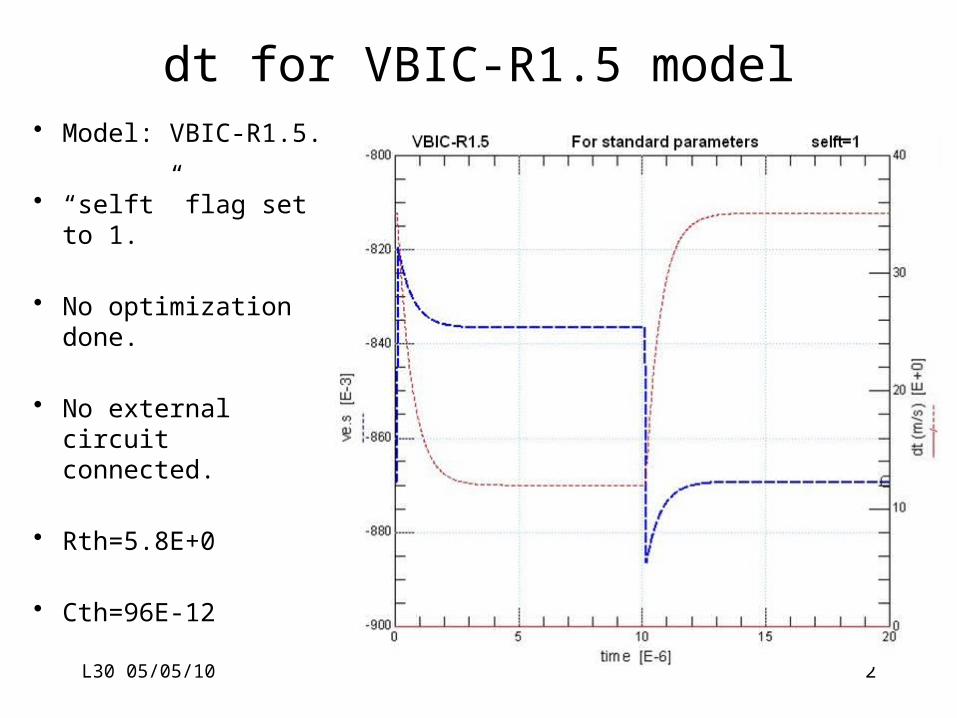
dt for VBIC-R1.5 model• Model: VBIC-R1.5.
• “selft” flag set to 1.
• No optimization done.
• No external circuit connected.
• Rth=5.8E+0
• Cth=96E-12
L30 05/05/10

3
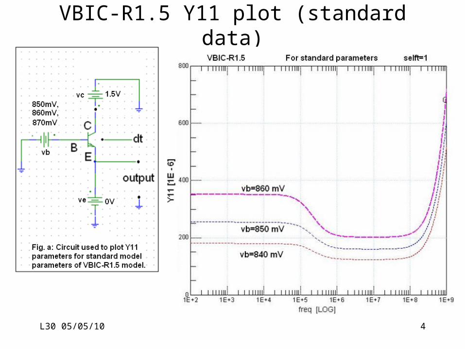
VBIC-R1.5 Y11 plot (standard data)
L30 05/05/10
4
VBIC-R1.5 Y11 plot (standard data)
L30 05/05/10

VBIC-R1.2 Y11 plot (optimized data)
5
• For optimized data refer slide “Model Parameters”.
• Circuit used is shown in “Circuit for Y parameters (optimized data)” slide.
fc Τ
fc1= 2E3 7.962E-05fc2=
9.25E4 1.721E-06fc3= 3.2E6 4.976E-08
Fc4=2E3 7.962E-05Fc5=1E5 1.592E-06Fc6=4E6 3.981E-08fc7= 2E3 7.962E-05fc8= 1E5 1.592E-06fc9=4E6 3.981E-08L30 05/05/10

Spreadsheet for Calculating the Rth and Cth• Calculations mentioned in the previous slides have
been implemented in an Excel spreadsheet.• The Cauer to Foster network transformation is done.
• The spreadsheet takes the dimensions of different layers of the devices and gives corresponding Cauer and Foster network values. This enables the calculation of time constants which can be converted into a single pole. The characteristic times for the Foster network appear on a impulse response plot.L30 05/05/10 6
Fig. 7. Electrical equivalent Cauer network of the HBT Fig. 8. Electrical equivalent Foster network of the HBT

IC-CAP Simulations
L30 05/05/10 7
8L30 05/05/10
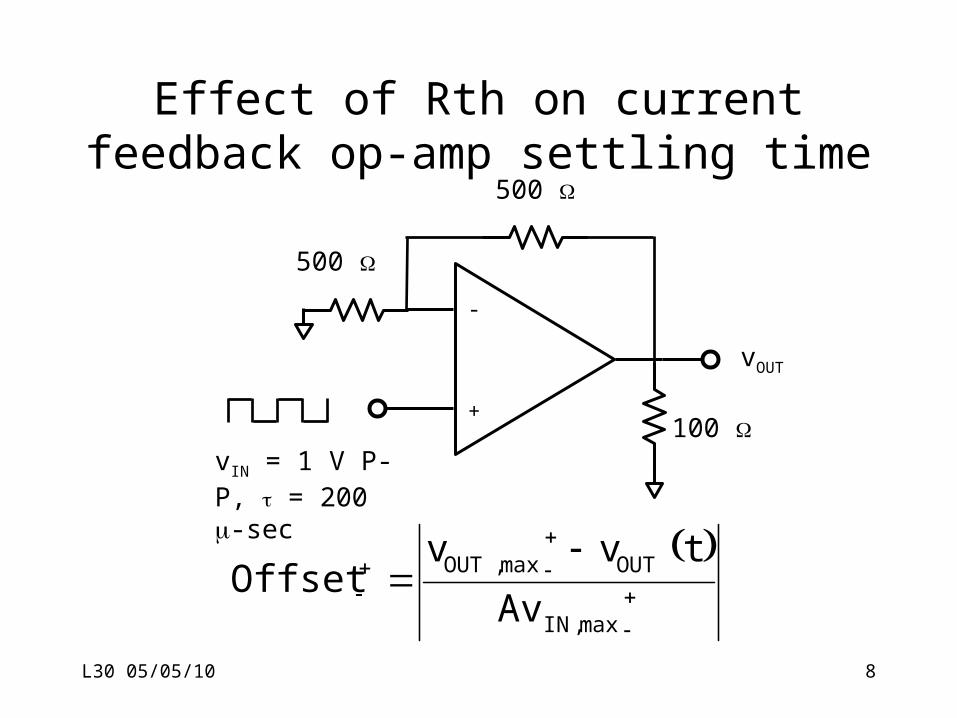
Effect of Rth on current feedback op-amp settling time
-
+
vIN = 1 V P-P, t = 200 m-sec
500 W
500 W
vOUT
100 W
max,IN
OUTmax,OUT
Av
tvvOffset

9L30 05/05/10
y = 0.0055e-0.1416x
Offset = 0.16%Tau = 7.1 u-sec
y = 0.0039e-0.0749x
Offset = .39%Tau = 13.4 u-sec
0.01%
0.10%
1.00%
0 5 10 15 20 25 30Time after switching (u-sec)
Th
erm
al
sw
itc
hin
g o
ffs
et
as
%
of
Vp
Current Feedback Op Amp Data (LMH6704) Switching Offset
3.3/t4.13/t e%16.0e%39.0model cfoa
3.34.13/%39.07.7/%55.0
%16.0Tau
10L30 05/05/10
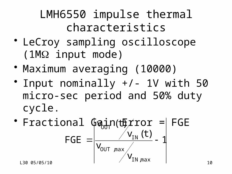
LMH6550 impulse thermal characteristics
• LeCroy sampling oscilloscope (1MW input mode)
• Maximum averaging (10000)• Input nominally +/- 1V with 50 micro-
sec period and 50% duty cycle.• Fractional Gain Error = FGE
1
vv
)t(v)t(v
FGE
max,IN
max,OUT
IN
OUT

11L30 05/05/10
vIN Rising Response
y = 0.0362e-111568x
R2 = 0.9707,Tau = 9 micro-sec
0.0
0.2
0.4
0.6
0.8
1.0
1.2
0.0E+00 5.0E-06 1.0E-05 1.5E-05 2.0E-05
0.10%
1.00%
10.00%
vOUT
vIN
FGE
12L30 05/05/10
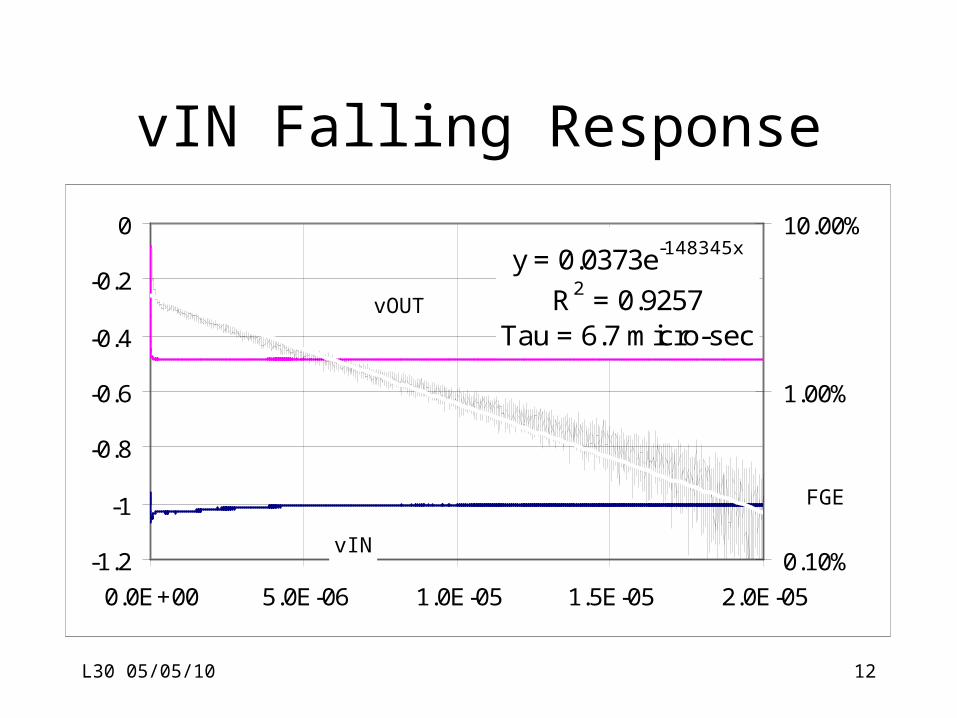
y = 0.0373e-148345x
R2 = 0.9257Tau = 6.7 micro-sec
-1.2
-1
-0.8
-0.6
-0.4
-0.2
0
0.0E+00 5.0E-06 1.0E-05 1.5E-05 2.0E-05
0.10%
1.00%
10.00%
vIN Falling Response
vOUT
vIN
FGE
13
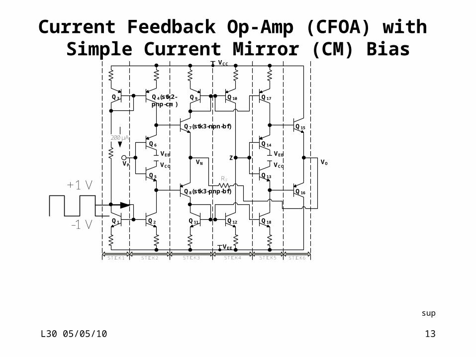
Current Feedback Op-Amp (CFOA) with Simple Current Mirror (CM) Bias
STICK1
VEE
VEE
VCC
VCC
Q1 Q2
Q3 Q4(stk2-pnp-cm)
Q11 Q12
Q9 Q10 Q17
Q18
Q14
Q13
Q15
Q16
VOZ
VN
STICK2 STICK3 STICK4 STICK5 STICK6
VEE
VCC
Q6
Q5
Q7(stk3-npn-bf)
Q8(stk3-pnp-bf)
VP
RF
200 μA
+1 V
-1 V
sup
L30 05/05/10

14
Large-signal Output Voltage Transient Analysis for CFOA with Simple CM Biasing
0 5 10 15 20 25 30 35 40 45-978
-976
-974
-972
-970
-968
Time (s)
Vo
ltag
e (
mV
)
0 5 10 15 20 25 30 35 40 45
1020
1022
1024
1026
1028
Time (s)
Vo
ltag
e (
mV
)
High-to-Low area x1
High-to-Low area x8
Low-to-High area x1
Low-to-High area x8
TT=-5311 V
TT=5313 V
TT=789 V
TT=-789 V
L30 05/05/10

15
Hypothesis: The Thermal Tail is a Linear Superposition of the Contribution from each
Individual Circuit Stick• The contribution of individual transistor to the total
thermal tail.
• Used six stick classifications according to transistor type and functionality.
i.e. Q10stk3-pnp-bf and Q11stk4-npn-cm
• Enabled the self-heating effect in the stick of interest and disabled the self-heating effect of the remaining transistors.
• Simulated the contribution of each individual stick.
• The total thermal tail simulated is essentially the sum of the individual thermal tail contributions of each circuit stick.
L30 05/05/10

16
The Hypothesis Supported Area x1 Area x8
Thermal Tail (uV/V) High-to-Low Low-to-High High-to-Low Low-to-High
stk2-npn-bf (Q5) -822 842 -124 128
stk2-pnp-bf (Q6) -727 712 -101 98
stk2-npn-cm (Q2) -89 91 -11 12
stk2-pnp-cm (Q4) -91 89 -10 9
stk3-npn-bf (Q7) -877 850 -111 106
stk3-pnp-bf (Q8) -783 808 -111 115
stk4-npn-cm (Q12) -1213 1217 -172 173
stk4-pnp-cm (Q10) -1075 1073 -159 158
stk5-npn-bf(Q13) 13 -13 2 -2
stk5-pnp-bf(Q14) -4 4 -1 1
stk5-npn-cm(Q18) 16 -15 2 -2
stk5-pnp-cm(Q17) -5 2 0 0
stk6-npn-bf(Q15) 0 1 0 0
stk6-pnp-bf(Q16) -1 0 0 0
added total -5658 5661 -796 796
simulated total -5311 5313 -789 789L30 05/05/10

L30 05/05/10 17

L30 05/05/10 18
HeterojunctionElectrostatics
Eo
EC,p
EV,p
EF,pEF,n
EC,n
EV,n
DEC
DEV
qfp
qfn
-xn xp0
L30 05/05/10 19
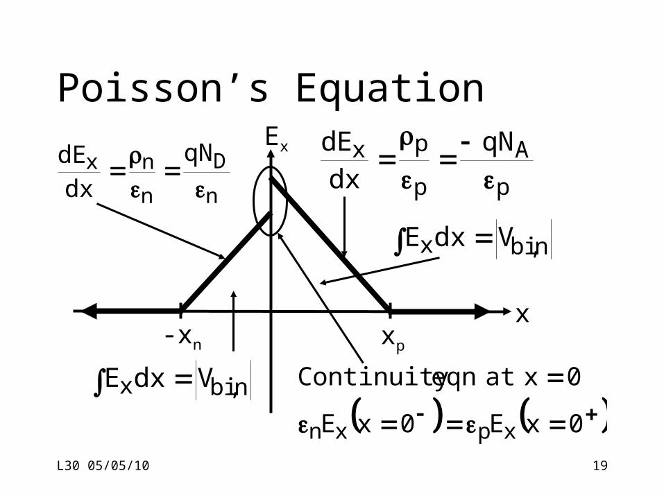
Poisson’s EquationEx
xxp-xn
p
A
p
px qNdxdE
n
D
n
nx qN
dxdE
n,bix VdxE
n,bix VdxE
0xE0xE
0x at eqn Continuity
xpxn

L30 05/05/10 20
Heterojunctionelectronics
d
2inonovn,vn,f
n,vn,fn,gnn
dcn,fc
n,fcnn,fon
npbi
pand
N/np , p/NlnkTEE
EEEqq
N/NlnkTEE
EEqEEq
V
xqNxqN ,neutrality Charge

L30 05/05/10 21
Heterojunctionelectronics (cont)
text. in 8.40 & 8.39 c.f.
, N/NlnkTEE
, EEEqq
. N/nn , n/NlnkTEE
, EEqEEq
avp,vp,f
p,vp,fp,gpp
a2ipopocp,fc
p,fcpp,fop

L30 05/05/10 22
Heterojunctionelectronics (cont)
form. eappropriat the is this then
E is barrier eappropriat the and
important, is injection hole Since
. /Nnp and , Np
, N
N
p
plnkTEqV
8.39 e.g.
v
d2inoapo
n,v
n,v
no
povbi

L30 05/05/10 23
Heterojunctiondepletion widths
p,apn,dnp,a
n,dbipnp
p,apn,dnn,d
p,abipnn
p,apn,dnp,an,d
2p,an,dbipn
pn
NNqN
NV2x
NNqN
NV2x
NNNqN
NNV2xxW
L30 05/05/10 24
References• Fujiang Lin, et al, “Extraction Of VBIC Model for SiGe
HBTs Made Easy by Going Through Gummel-Poon Model”, from http://eesof.tm.agilent.com/pdf/VBIC_Model_Extraction.pdf
• http://www.fht-esslingen.de/institute/iafgp/neu/VBIC/• Avanti Star-spice User Manual, 04, 2001. • Affirma Spectre Circuit Simulator Device Model
Equations• Zweidinger, D.T.; Fox, R.M., et al, “Equivalent circuit
modeling of static substrate thermal coupling using VCVS representation”, Solid-State Circuits, IEEE Journal of , Volume: 2 Issue: 9 , Sept. 2002, Page(s): 1198 -1206

Thermal Analogy References
[1] I.Z. Mitrovic , O. Buiu, S. Hall, D.M. Bagnall and P. Ashburn “Review of SiGe HBTs on SOI”, Solid State Electronics, Sept. 2005, Vol. 49, pp. 1556-1567.
[2] Masana, F. N., “A New Approach to the Dynamic Thermal Modeling of Semiconductor Packages”, Microelectron. Reliab., 41, 2001, pp. 901–912.
[3] Richard C. Joy and E. S. Schlig, “Thermal Properties of Very Fast Transistors”, IEEE Trans. ED, ED-1 7. No. 8, August 1970, pp. 586-599.
[4] Kevin Bastin, “Analysis and Modeling of self heating in SiGe HBTs” , Aug. 2009, Masters Thesis, UTA.
[5] Rinaldi, N., “On the Modeling of the Transient Thermal Behavior of Semiconductor Devices”, IEEE Trans-ED, Volume: 48 , Issue: 12 , Dec. 2001; Pages:2796 – 2802.
L30 05/05/10 25

26
Simulation … References• [1] E. Castro, S. Coco, A. Laudani, L. LO Nigro and G. Pollicino, “A New Tool For
Bipolar Transistor Characterization Based on HICUM”, Communications to SIMAI Congress, ISSN 1827-9015, Vol. 2, 2007.
• [2] K. Bastin, “Analysis And Modeling of Self Heating in Silicon Germanium Heterojunction Bipolar Transistors”, Thesis report, The University of Texas at Arlington, August 2009.
L30 05/05/10

27
AICR Team at University of Texas Arlington - Electrical Engineering
Current• Ronald L. Carter, Professor• W. Alan Davis, Associate
Professor• Howard T. Russell, Senior
Lecturer• Ardasheir Rahman1
• Ratan Pulugurta1
• Xuesong Xie1
• Arun Thomas-Karingada2
• Sharath Patil2
• Valay Shah2
Earlier Contributors• Kevin Bastin, MS• Abhijit Chaugule, MS• Daewoo Kim, PhD• Anurag Lakhlani, MS• Zheng Li, PhD• Kamal Sinha, PhD
1PhD Student2MS Student
L30 05/05/10


