
EE1411
© Digital Integrated Circuits2nd Inverter
Digital Integrated Digital Integrated CircuitsCircuitsA Design PerspectiveA Design Perspective
The InverterThe Inverter
Jan M. RabaeyAnantha ChandrakasanBorivoje Nikolic
July 30, 2002
EE1412
© Digital Integrated Circuits2nd Inverter
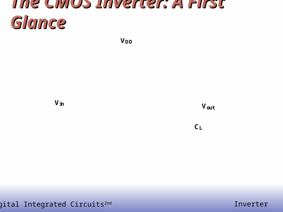
The CMOS Inverter: A First GlanceThe CMOS Inverter: A First GlanceVDD
Vin Vout
CL

EE1413
© Digital Integrated Circuits2nd Inverter
CMOS InvertersCMOS Inverters
Polysilicon
InOut
Metal1
VDD
GND
PMOS
NMOS
2

EE1414
© Digital Integrated Circuits2nd Inverter
Voltage TransferVoltage TransferCharacteristicCharacteristic
EE1415
© Digital Integrated Circuits2nd Inverter
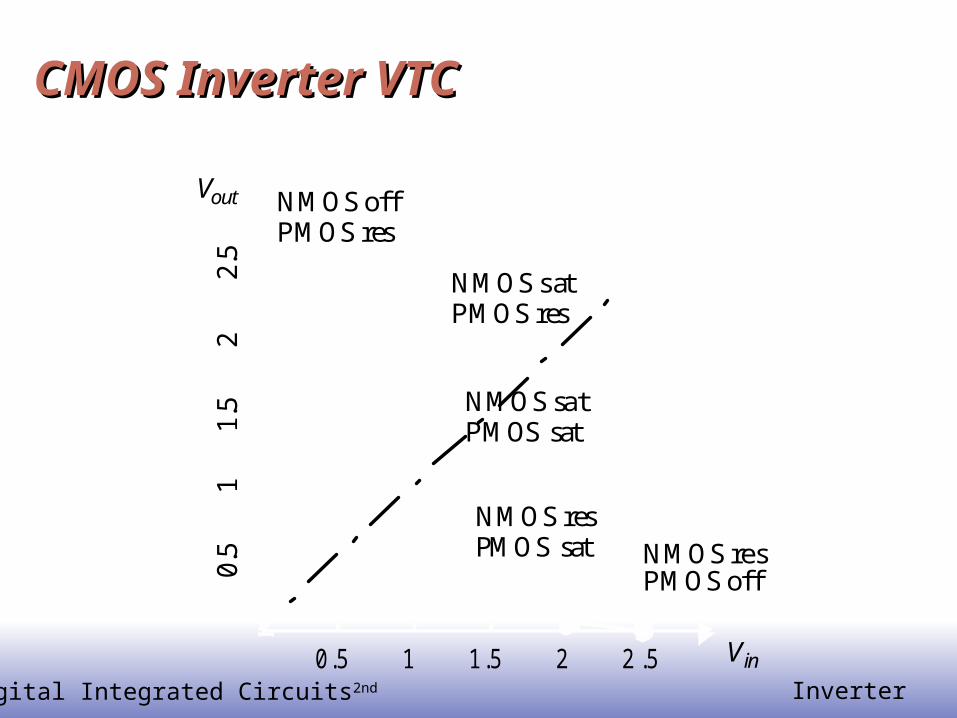
CMOS Inverter VTCCMOS Inverter VTC
Vout
Vin0.5 1 1.5 2 2 .5
0.5
11.
52
2.5
NMOS resPMOS off
NMOS satPMOS sat
NMOS offPMOS res
NMOS satPMOS res
NMOS resPMOS sat

EE1416
© Digital Integrated Circuits2nd Inverter
Switching Threshold as a function Switching Threshold as a function of Transistor Ratioof Transistor Ratio
100
101
0.8
0.9
1
1.1
1.2
1.3
1.4
1.5
1.6
1.7
1.8
MV
(V
)
Wp
/Wn

EE1417
© Digital Integrated Circuits2nd Inverter
Impact of Process VariationsImpact of Process Variations
0 0.5 1 1.5 2 2.50
0.5
1
1.5
2
2.5
Vin (V)
Vo
ut(V
)
Good PMOSBad NMOS
Good NMOSBad PMOS
Nominal

EE1418
© Digital Integrated Circuits2nd Inverter
Propagation DelayPropagation Delay

EE1419
© Digital Integrated Circuits2nd Inverter
CMOS Inverter Propagation DelayCMOS Inverter Propagation DelayApproach 1Approach 1
VDD
Vout
Vin = VDD
CLIav
tpHL = CL Vswing/2
Iav
CL
kn VDD
~

EE14110
© Digital Integrated Circuits2nd Inverter
CMOS Inverter Propagation DelayCMOS Inverter Propagation DelayApproach 2Approach 2
VDD
Vout
Vin = VDD
Ron
CL
tpHL = f(Ron.CL)
= 0.69 RonCL
t
Vout
VDD
RonCL
1
0.5
ln(0.5)
0.36

EE14111
© Digital Integrated Circuits2nd Inverter
0 0.5 1 1.5 2 2.5
x 10-10
-0.5
0
0.5
1
1.5
2
2.5
3
t (sec)
Vou
t(V)
Transient ResponseTransient Response
tp = 0.69 CL (Reqn+Reqp)/2
?
tpLHtpHL

EE14112
© Digital Integrated Circuits2nd Inverter
Design for PerformanceDesign for Performance
Keep capacitances small Increase transistor sizes
watch out for self-loading!
Increase VDD (????)

EE14113
© Digital Integrated Circuits2nd Inverter
Delay as a function of VDelay as a function of VDDDD
0.8 1 1.2 1.4 1.6 1.8 2 2.2 2.41
1.5
2
2.5
3
3.5
4
4.5
5
5.5
VDD
(V)
t p(nor
mal
ized
)

EE14114
© Digital Integrated Circuits2nd Inverter
2 4 6 8 10 12 142
2.2
2.4
2.6
2.8
3
3.2
3.4
3.6
3.8x 10
-11
S
t p(sec
)
Device SizingDevice Sizing
(for fixed load)
Self-loading effect:Intrinsic capacitancesdominate

EE14115
© Digital Integrated Circuits2nd Inverter
1 1.5 2 2.5 3 3.5 4 4.5 53
3.5
4
4.5
5x 10
-11
t p(sec
)
NMOS/PMOS ratioNMOS/PMOS ratio
tpLH tpHL
tp = Wp/Wn

EE14116
© Digital Integrated Circuits2nd Inverter
Inverter SizingInverter Sizing

EE14117
© Digital Integrated Circuits2nd Inverter
Inverter ChainInverter Chain
CL
If CL is given:- How many stages are needed to minimize the delay?- How to size the inverters?
May need some additional constraints.
In Out
EE14118
© Digital Integrated Circuits2nd Inverter
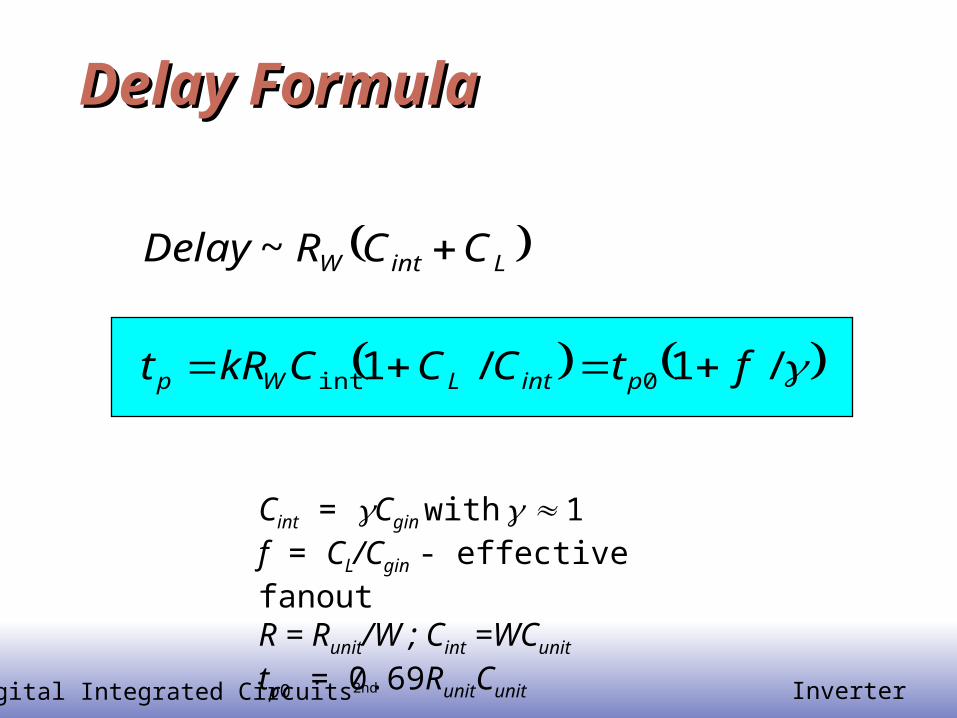
Delay FormulaDelay Formula
/1/1
~
0int ftCCCkRt
CCRDelay
pintLWp
LintW
Cint = Cgin with 1f = CL/Cgin - effective fanoutR = Runit/W ; Cint =WCunit
tp0 = 0.69RunitCunit

EE14119
© Digital Integrated Circuits2nd Inverter
Apply to Inverter ChainApply to Inverter Chain
CL
In Out
1 2 N
tp = tp1 + tp2 + …+ tpN
jgin
jginunitunitpj C
CCRt
,
1,1~
LNgin
N
i jgin
jginp
N
jjpp CC
C
Cttt
1,
1 ,
1,0
1, ,1

EE14120
© Digital Integrated Circuits2nd Inverter
Optimal Tapering for Given Optimal Tapering for Given NN
Delay equation has N - 1 unknowns, Cgin,2 – Cgin,N
Minimize the delay, find N - 1 partial derivatives
Result: Cgin,j+1/Cgin,j = Cgin,j/Cgin,j-1
Size of each stage is the geometric mean of two neighbors
- each stage has the same effective fanout (Cout/Cin)- each stage has the same delay
1,1,, jginjginjgin CCC

EE14121
© Digital Integrated Circuits2nd Inverter
Optimum Delay and Number of Optimum Delay and Number of StagesStages
1,/ ginLN CCFf
When each stage is sized by f and has same eff. fanout f:
N Ff
/10N
pp FNtt
Minimum path delay
Effective fanout of each stage:

EE14122
© Digital Integrated Circuits2nd Inverter
ExampleExample
CL= 8 C1
In Out
C11 f f2
283 f
CL/C1 has to be evenly distributed across N = 3 stages:

EE14123
© Digital Integrated Circuits2nd Inverter
Optimum Number of StagesOptimum Number of Stages
For a given load, CL and given input capacitance Cin
Find optimal sizing f
ff
fFtFNtt pN
pp lnln
ln1/ 0/1
0
0ln
1lnln2
0
f
ffFt
f
t pp
For = 0, f = e, N = lnF
f
FNCfCFC in
NinL ln
ln with
ff 1exp

EE14124
© Digital Integrated Circuits2nd Inverter
Optimum Effective Fanout Optimum Effective Fanout ffOptimum f for given process defined by
ff 1exp
fopt = 3.6for =1
EE14125
© Digital Integrated Circuits2nd Inverter
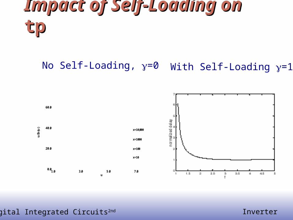
Impact of Self-Loading on Impact of Self-Loading on tptp
1.0 3.0 5.0 7.0u
0.0
20.0
40.0
60.0
u/l
n(u
)
x=10
x=100
x=1000
x=10,000
No Self-Loading, =0 With Self-Loading =1

EE14126
© Digital Integrated Circuits2nd Inverter
Normalized delay function of Normalized delay function of FF
/10N
pp FNtt

EE14127
© Digital Integrated Circuits2nd Inverter
Buffer DesignBuffer Design
1
1
1
1
8
64
64
64
64
4
2.8 8
16
22.6
N f tp
1 64 65
2 8 18
3 4 15
4 2.8 15.3

EE14128
© Digital Integrated Circuits2nd Inverter
Power DissipationPower Dissipation

EE14129
© Digital Integrated Circuits2nd Inverter
Where Does Power Go in CMOS?Where Does Power Go in CMOS?
• Dynamic Power Consumption
• Short Circuit Currents
• Leakage
Charging and Discharging Capacitors
Short Circuit Path between Supply Rails during Switching
Leaking diodes and transistors

EE14130
© Digital Integrated Circuits2nd Inverter
Dynamic Power DissipationDynamic Power Dissipation
Energy/transition = CL * Vdd2
Power = Energy/transition * f = CL * Vdd2 * f
Need to reduce CL, Vdd, and f to reduce power.
Vin Vout
CL
Vdd
Not a function of transistor sizes!

EE14131
© Digital Integrated Circuits2nd Inverter
Modification for Circuits with Reduced Swing
CL
Vdd
Vdd
Vdd -Vt
E0 1 CL Vdd Vdd Vt– =
Can exploit reduced swing to lower power(e.g., reduced bit-line swing in memory)

EE14132
© Digital Integrated Circuits2nd Inverter
Adiabatic Charging
22
2

EE14133
© Digital Integrated Circuits2nd Inverter
Adiabatic Charging

EE14134
© Digital Integrated Circuits2nd Inverter
Node Transition Activity and PowerNode Transition Activity and PowerConsider switching a CMOS gate for N clock cycles
EN CL Vdd 2 n N =
n(N): the number of 0->1 transition in N clock cycles
EN : the energy consumed for N clock cycles
Pavg N lim
ENN
-------- fclk= n N
N------------
N lim
C
LVdd
2fclk
=
0 1
n N N
------------N
lim=
Pavg = 0 1 C
LVdd
2 fclk

EE14135
© Digital Integrated Circuits2nd Inverter
Transistor Sizing for Minimum Transistor Sizing for Minimum EnergyEnergy
Goal: Minimize Energy of whole circuit Design parameters: f and VDD
tp tpref of circuit with f=1 and VDD =Vref
1Cg1
In
fCext
Out
TEDD
DDp
pp
VV
Vt
f
Fftt
0
0 11

EE14136
© Digital Integrated Circuits2nd Inverter
Transistor Sizing (2)Transistor Sizing (2) Performance Constraint (=1)
Energy for single Transition
13
2
3
2
0
0
F
fF
f
VV
VV
V
V
F
fF
f
t
t
t
t
TEDD
TEref
ref
DD
refp
p
pref
p
F
Ff
V
V
E
E
FfCVE
ref
DD
ref
gDD
4
22
112
12

EE14137
© Digital Integrated Circuits2nd Inverter
1 2 3 4 5 6 70
0.5
1
1.5
2
2.5
3
3.5
4
f
vdd
(V
)
1 2 3 4 5 6 70
0.5
1
1.5
f
no
rma
lize
d e
ne
rgy
Transistor Sizing (3)Transistor Sizing (3)
F=1
2
5
10
20
VDD=f(f) E/Eref=f(f)
EE14138
© Digital Integrated Circuits2nd Inverter
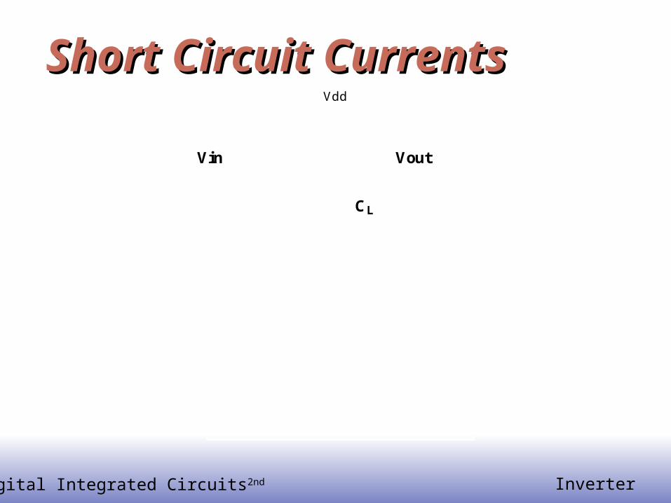
Short Circuit CurrentsShort Circuit Currents
Vin Vout
CL
Vdd
I VD
D (m
A)
0.15
0.10
0.05
Vin (V)5.04.03.02.01.00.0

EE14139
© Digital Integrated Circuits2nd Inverter
How to keep Short-Circuit Currents Low?How to keep Short-Circuit Currents Low?
Short circuit current goes to zero if tfall >> trise,but can’t do this for cascade logic, so ...

EE14140
© Digital Integrated Circuits2nd Inverter
Minimizing Short-Circuit PowerMinimizing Short-Circuit Power
0 1 2 3 4 50
1
2
3
4
5
6
7
8
tsin
/tsout
Pno
rm
Vdd =1.5
Vdd =2.5
Vdd =3.3

EE14141
© Digital Integrated Circuits2nd Inverter
LeakageLeakage
Vout
Vdd
Sub-ThresholdCurrent
Drain JunctionLeakage
Sub-Threshold Current Dominant FactorSub-threshold current one of most compelling issuesin low-energy circuit design!

EE14142
© Digital Integrated Circuits2nd Inverter
Reverse-Biased Diode LeakageReverse-Biased Diode Leakage
Np+ p+
Reverse Leakage Current
+
-Vdd
GATE
IDL = JS A
JS = 1-5pA/m2 for a 1.2m CMOS technology
Js double with every 9oC increase in temperature
JS = 10-100 pA/m2 at 25 deg C for 0.25m CMOSJS doubles for every 9 deg C!

EE14143
© Digital Integrated Circuits2nd Inverter
Subthreshold Leakage ComponentSubthreshold Leakage Component
EE14144
© Digital Integrated Circuits2nd Inverter
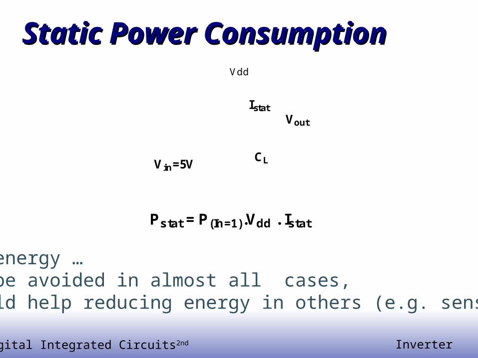
Static Power ConsumptionStatic Power Consumption
Vin=5V
Vout
CL
Vdd
Istat
Pstat = P(In=1).Vdd . Istat
• Dominates over dynamic consumption
• Not a function of switching frequency
Wasted energy …Should be avoided in almost all cases,but could help reducing energy in others (e.g. sense amps)

EE14145
© Digital Integrated Circuits2nd Inverter
Principles for Power ReductionPrinciples for Power Reduction
Prime choice: Reduce voltage! Recent years have seen an acceleration in
supply voltage reduction Design at very low voltages still open question
(0.6 … 0.9 V by 2010!) Reduce switching activity Reduce physical capacitance
Device Sizing: for F=20– fopt(energy)=3.53, fopt(performance)=4.47


