
1
6-1
EE105 – Fall 2015 Microelectronic Devices and Circuits
Prof. Ming C. Wu
511 Sutardja Dai Hall (SDH)
6-2
pn Junction
• p-type semiconductor in contact with n-type
• Basic building blocks of semiconductor devices – Diodes, – Bipolar junction transistors (BJT), – Metal-oxide-semiconductor field effect transistors (MOSFET)
2
6-3
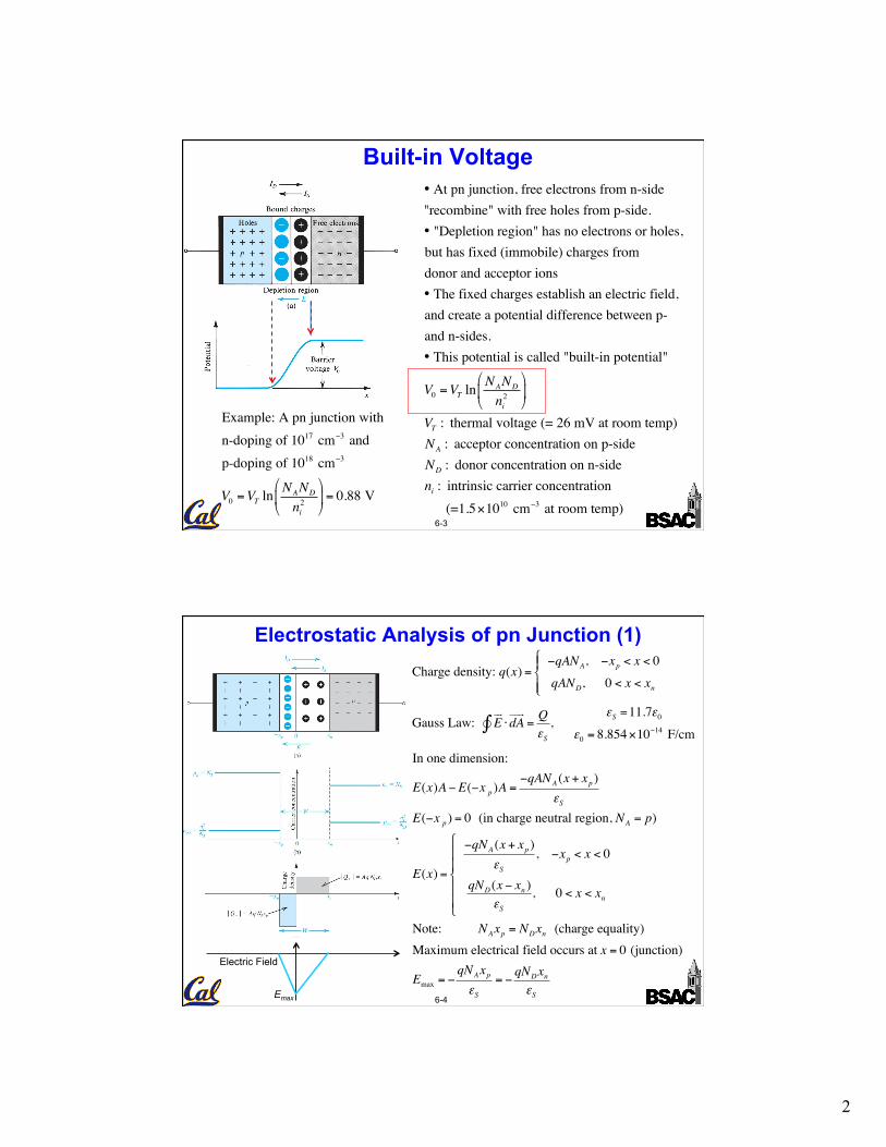
Built-in Voltage • At pn junction, free electrons from n-side
"recombine" with free holes from p-side.• "Depletion region" has no electrons or holes, but has fixed (immobile) charges fromdonor and acceptor ions• The fixed charges establish an electric field, and create a potential difference between p-and n-sides. • This potential is called "built-in potential"
V0 =VT ln NAND
ni2
!
"#
$
%&
VT : thermal voltage (= 26 mV at room temp)NA : acceptor concentration on p-sideND : donor concentration on n-sideni : intrinsic carrier concentration (=1.5×1010 cm−3 at room temp)
Example: A pn junction with n-doping of 1017 cm−3 and p-doping of 1018 cm−3
V0 =VT ln NAND
ni2
"
#$
%
&'= 0.88 V
6-4
Electrostatic Analysis of pn Junction (1)
Charge density: q(x) =−qANA, −xp < x < 0
qAND, 0 < x < xn
"#$
%$
Gauss Law: E!"⋅dA! "!
#∫ =QεS
, εS =11.7ε0
ε0 = 8.854×10⁻¹⁴ F/cm
In one dimension:
E(x)A−E(−x p )A =−qANA (x + xp )
εSE(−x p ) = 0 (in charge neutral region, NA = p)
E(x) =
−qNA (x + xp )εS
, −xp < x < 0
qND (x − xn )εS
, 0 < x < xn
"
#
$$
%
$$
Note: NAxp = NDxn (charge equality)Maximum electrical field occurs at x = 0 (junction)
Emax = −qNAxpεS
= −qNDxnεSEmax
Electric Field
3
6-5
Electrostatic Analysis of pn Junction (2)
Emax
Electric Field
E(x) =
−qNA (x + xp )εS
, −xp < x < 0
qND (x − xn )εS
, 0 < x < xn
"
#
$$
%
$$
V (x) = − E(x ')dx '−xp
x
∫
V (x) =
qNA
2εSx + xp( )
2, −xp < x < 0
q2εS
NAxp2 + NDxn
2( )− qND
2εSx − xn( )2 , 0 < x < xn
"
#
$$
%
$$
V (x n ) = q2εS
NAxp2 + NDxn
2( ) =V0
xp =ND
NA + ND
W, xn =NA
NA + ND
W
W =2eSq
1NA
+1ND
'
()
*
+,V0 : Depletion Width
6-6
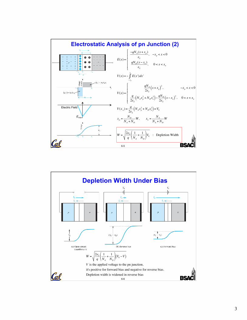
Depletion Width Under Bias
W =2eSq
1NA
+1ND
!
"#
$
%& V0 −V( )
V is the applied voltage to the pn junction, it's positive for forward bias and negative for reverse bias.Depletion width is widened in reverse bias

4
6-7
Current-Voltage (I-V) Characteristics
Under forward bias, minority carriersat the edge of depletion region is boostedup by (eV /VT −1) :
pn (x) = pn0 + pn0 eV /VT −1( ) ⋅e−x−xnLp
Lp : hole diffusion length in n-typeHole diffusion current density on n-side
Jp = −qDpdpn (x)dx x=xn
= qDp
Lp
pn0 eV /VT −1( )
Similarly, electron diffusion current density in p-side
Jn = qDn
dnp(x)dx x=−xp
= q Dn
Lnnp0 eV /VT −1( )
Total current :
I = Jp + Jn( )A = A qDp
Lp
pn0 + qDn
Lnnp0
"
#$$
%
&'' e
V /VT −1( )
I = IS eV /VT −1( ) where IS = Aqni
2 Dp
LpND
+Dn
LnNA
"
#$$
%
&''
6-8
I-V Curve
I = IS eV /VT −1( )
where
IS = Aqni2 Dp
LpND
+Dn
LnNA
"
#$$
%
&''

5
6-9
Capacitance in pn Junction (1):
Depletion Capacitance (Mainly Reverse Bias)
Total charge Ain depletion width at V = -VR
QJ = AqNDxn = AqNDNA
NA + ND
W
W =2eSq
1NA
+1ND
!
"#
$
%& V0 +VR( )
As bias voltage change, the amount of charge in the junction change. This is a "nonlinear" capacitor. The capacitance value is
Cj =dQJ
dVR= Aq NDNA
NA + ND
2eSq
1NA
+1ND
!
"#
$
%&ddV
V0 +VR( )
Cj = AεSq2
NAND
NA + ND
!
"#
$
%&
1V0 +VR( )
Note: Cj =εSAW
At zero bias, VR = 0
Cj0 = AεSq2
NAND
NA + ND
!
"#
$
%&
1V0
Therefore at V = -VR , Cj =Cj0
1+VRV0
This is a variable capacitor, controllable by voltage !
In comparision, for a "linear" (normal) capacitor:
C = QV
is a constant
6-10
Capacitance in pn Junction (2): Diffusion Capacitance (Forward Bias)
Extra minority carriers stored outside junction under forward bias
Qp = Aq× shaded area under pn (x)
Qp = Aq pn0 eV /VT −1( ) ⋅e−x−xnLp
xn
∞
∫ dx
Qp = AqLppn0 eV /VT −1( ) = Lp2
Dp
Ip = τ pI p
Lp2
Dp
has unit of time, its physical meaning is
minority carrier lifetime: τ p =Lp
2
Dp
Similarly, Qn = τ nInTotal charge stored : Q = τ pI p +τ nIn = τ T Iτ T is mean transit timeThese stored charges correspond to another nonlinear capacitor call "diffusion capacitance":
Cd =dQdV
=d τ T I( )dV
= τ TdIdV
⇒ Cd =τ TVT
'
()
*
+,I

6
6-11
Summary of pn Junction Built-in potential : V0 =VT ln NAND
ni2
!
"#
$
%&
Under forward bias :
I-V curve : I = IS eV /VT −1( )
Diffusion capacitance : Cd =τ TVT
!
"#
$
%&I
Under revserse bias : Negligible current, I = −IS
Depletion capacitance : Cj =Cj0
1+VRV0
Other important parameter :
Depletion Width: W =2eSq
1NA
+1ND
!
"#
$
%& V0 −V( )
6-12
Detailed Derivation of pn Junction Potential
E(x) =
−qNA (x + xp )εS
, −xp < x < 0
qND (x − xn )εS
, 0 < x < xn
"
#
$$
%
$$
V (x) = − E(x ')dx '−xp
x
∫
(1) for − xp < x < 0 :V (x) = − E(x ')dx '−xp
x
∫ =qNA (x '+ xp )
εSdx '
−xp
x
∫ =qNA
2εSx '+ xp( )
2
x '=−xp
x '=x
=qNA
2εSx + xp( )
2
(2) for 0 < x < xn : Because E(x) has different expression for x < 0 and x > 0, the integration should
be performed in two separate ranges, first from − xp to 0, and then from 0 to x. We can use V (x = 0) from the above equation for the first intgration. Therefore,
V (x) = qNA
2εSxp
2 −qND (x '− xn )
εSdx '
0
x
∫ =qNA
2εSxp
2 −qND (x '− xn )2
2εS 0
x
=qNA
2εSxp
2 −qND (x − xn )2
2εS−qNDxn
2
2εS
'
()
*
+,=
qNA
2εSxp
2 +qNDxn
2
2εS−qND (x − xn )2
2εS
Built-in potential : V0 =V (x n ) = q2εS
NAxp2 + NDxn
2( )


