
© 2005 Microchip Technology Inc. Preliminary DS70141B
dsPIC30F3010/3011Data Sheet
High PerformanceDigital Signal Controllers

Note the following details of the code protection feature on Microchip devices:
• Microchip products meet the specification contained in their particular Microchip Data Sheet.
• Microchip believes that its family of products is one of the most secure families of its kind on the market today, when used in the intended manner and under normal conditions.
• There are dishonest and possibly illegal methods used to breach the code protection feature. All of these methods, to our knowledge, require using the Microchip products in a manner outside the operating specifications contained in Microchip’s Data Sheets. Most likely, the person doing so is engaged in theft of intellectual property.
• Microchip is willing to work with the customer who is concerned about the integrity of their code.
• Neither Microchip nor any other semiconductor manufacturer can guarantee the security of their code. Code protection does not mean that we are guaranteeing the product as “unbreakable.”
Code protection is constantly evolving. We at Microchip are committed to continuously improving the code protection features of ourproducts. Attempts to break Microchip’s code protection feature may be a violation of the Digital Millennium Copyright Act. If such actsallow unauthorized access to your software or other copyrighted work, you may have a right to sue for relief under that Act.
Information contained in this publication regarding deviceapplications and the like is provided only for your convenienceand may be superseded by updates. It is your responsibility toensure that your application meets with your specifications.MICROCHIP MAKES NO REPRESENTATIONS OR WAR-RANTIES OF ANY KIND WHETHER EXPRESS OR IMPLIED,WRITTEN OR ORAL, STATUTORY OR OTHERWISE,RELATED TO THE INFORMATION, INCLUDING BUT NOTLIMITED TO ITS CONDITION, QUALITY, PERFORMANCE,MERCHANTABILITY OR FITNESS FOR PURPOSE.Microchip disclaims all liability arising from this information andits use. Use of Microchip’s products as critical components inlife support systems is not authorized except with expresswritten approval by Microchip. No licenses are conveyed,implicitly or otherwise, under any Microchip intellectual propertyrights.
DS70141B-page ii Prelimin
Trademarks
The Microchip name and logo, the Microchip logo, Accuron, dsPIC, KEELOQ, microID, MPLAB, PIC, PICmicro, PICSTART, PRO MATE, PowerSmart, rfPIC, and SmartShunt are registered trademarks of Microchip Technology Incorporated in the U.S.A. and other countries.
AmpLab, FilterLab, Migratable Memory, MXDEV, MXLAB, PICMASTER, SEEVAL, SmartSensor and The Embedded Control Solutions Company are registered trademarks of Microchip Technology Incorporated in the U.S.A.
Analog-for-the-Digital Age, Application Maestro, dsPICDEM, dsPICDEM.net, dsPICworks, ECAN, ECONOMONITOR, FanSense, FlexROM, fuzzyLAB, In-Circuit Serial Programming, ICSP, ICEPIC, MPASM, MPLIB, MPLINK, MPSIM, PICkit, PICDEM, PICDEM.net, PICLAB, PICtail, PowerCal, PowerInfo, PowerMate, PowerTool, rfLAB, rfPICDEM, Select Mode, Smart Serial, SmartTel and Total Endurance are trademarks of Microchip Technology Incorporated in the U.S.A. and other countries.
SQTP is a service mark of Microchip Technology Incorporated in the U.S.A.
All other trademarks mentioned herein are property of their respective companies.
© 2005, Microchip Technology Incorporated, Printed in the U.S.A., All Rights Reserved.
Printed on recycled paper. 11/12/04
ary © 2005 Microchip Technology Inc.
Microchip received ISO/TS-16949:2002 quality system certification for its worldwide headquarters, design and wafer fabrication facilities in Chandler and Tempe, Arizona and Mountain View, California in October 2003. The Company’s quality system processes and procedures are for its PICmicro® 8-bit MCUs, KEELOQ® code hopping devices, Serial EEPROMs, microperipherals, nonvolatile memory and analog products. In addition, Microchip’s quality system for the design and manufacture of development systems is ISO 9001:2000 certified.

dsPIC30F3010/3011dsPIC30F3010/3011 Enhanced Flash
16-bit Digital Signal Controller
High Performance Modified RISC CPU:
• Modified Harvard architecture• C compiler optimized instruction set architecture
with flexible addressing modes• 84 base instructions
• 24-bit wide instructions, 16-bit wide data path• 24 Kbytes on-chip Flash program space
(8K Instruction words)• 1 Kbytes of on-chip data RAM• 1 Kbytes of non-volatile data EEPROM
• 16 x 16-bit working register array• Up to 30 MIPs operation:
- DC to 40 MHz external clock input
- 4 MHz-10 MHz oscillator input with PLL active (4x, 8x, 16x)
• 29 interrupt sources- 3 external interrupt sources- 8 user selectable priority levels for each
interrupt source- 4 processor trap sources
DSP Engine Features:
• Dual data fetch
• Accumulator write back for DSP operations • Modulo and Bit-Reversed Addressing modes• Two, 40-bit wide accumulators with optional
saturation logic• 17-bit x 17-bit single cycle hardware fractional/
integer multiplier• All DSP instructions single cycle
• ± 16-bit single cycle shift
Peripheral Features:
• High current sink/source I/O pins: 25 mA/25 mA• Timer module with programmable prescaler:
- Five 16-bit timers/counters; optionally pair 16-bit timers into 32-bit timer modules
• 16-bit Capture input functions• 16-bit Compare/PWM output functions• 3-wire SPITM modules (supports 4 Frame modes)
• I2CTM module supports Multi-Master/Slave mode and 7-bit/10-bit addressing
• 2 UART modules with FIFO Buffers
Motor Control PWM Module Features:
• 6 PWM output channels- Complementary or Independent Output
modes- Edge and Center-Aligned modes
• 3 duty cycle generators
• Dedicated time base• Programmable output polarity• Dead-time control for Complementary mode
• Manual output control• Trigger for A/D conversions
Quadrature Encoder Interface Module Features:
• Phase A, Phase B and Index Pulse input
• 16-bit up/down position counter • Count direction status• Position Measurement (x2 and x4) mode
• Programmable digital noise filters on inputs• Alternate 16-bit Timer/Counter mode• Interrupt on position counter rollover/underflow
Note: This data sheet summarizes features of this groupof dsPIC30F devices and is not intended to be a completereference source. For more information on the CPU,peripherals, register descriptions and general devicefunctionality, refer to the dsPIC30F Family ReferenceManual (DS70046). For more information on the deviceinstruction set and programming, refer to the dsPIC30FProgrammer’s Reference Manual (DS70030).
© 2005 Microchip Technology Inc. Preliminary DS70141B-page 1

dsPIC30F3010/3011
Analog Features:
• 10-bit Analog-to-Digital Converter (A/D) with4 S/H Inputs:- 500 Ksps conversion rate
- 9 input channels- Conversion available during Sleep and Idle
• Programmable Brown-out Detection and Reset generation
Special Microcontroller Features:
• Enhanced Flash program memory:- 10,000 erase/write cycle (min.) for
industrial temperature range, 100K (typical)• Data EEPROM memory:
- 100,000 erase/write cycle (min.) for industrial temperature range, 1M (typical)
• Self-reprogrammable under software control
• Power-on Reset (POR), Power-up Timer (PWRT) and Oscillator Start-up Timer (OST)
• Flexible Watchdog Timer (WDT) with on-chip low power RC oscillator for reliable operation
• Fail-Safe clock monitor operation detects clock failure and switches to on-chip low power RC oscillator
• Programmable code protection• In-Circuit Serial Programming™ (ICSP™)• Selectable Power Management modes
- Sleep, Idle and Alternate Clock modes
CMOS Technology:
• Low power, high speed Flash technology• Wide operating voltage range (2.5V to 5.5V)• Industrial and Extended temperature ranges
• Low power consumption
dsPIC30F Motor Control and Power Conversion Family*
Device PinsProgram
Mem. Bytes/Instructions
SRAMBytes
EEPROMBytes
Timer 16-bit
InputCap
OutputComp/Std
PWM
MotorControl
PWM
A/D 10-bit 500 Ksps
Quad Enc U
AR
T
SP
ITM
I2 CT
M
CA
N
dsPIC30F2010 28 12K/4K 512 1024 3 4 2 6 ch 6 ch Yes 1 1 1 -
dsPIC30F3010 28 24K/8K 1024 1024 5 4 2 6 ch 6 ch Yes 1 1 1 -
dsPIC30F4012 28 48K/16K 2048 1024 5 4 2 6 ch 6 ch Yes 1 1 1 1
dsPIC30F3011 40/44 24K/8K 1024 1024 5 4 4 6 ch 9 ch Yes 2 1 1 -
dsPIC30F4011 40/44 48K/16K 2048 1024 5 4 4 6 ch 9 ch Yes 2 1 1 1
dsPIC30F5015 64 66K/22K 2048 1024 5 4 4 8 ch 16 ch Yes 1 2 1 1
dsPIC30F6010 80 144K/48K 8192 4096 5 8 8 8 ch 16 ch Yes 2 2 1 2
* This table provides a summary of the dsPIC30F3010/3011 peripheral features. Other available devices in the dsPIC30F Motor Control and Power Conversion Family are shown for feature comparison.
DS70141B-page 2 Preliminary © 2005 Microchip Technology Inc.

dsPIC30F3010/3011
Pin Diagrams
AN7/RB7AN6/OCFA/RB6
RF0RF1
OC3/RD2EMUC2/OC1/IC1/INT1/RD0
AN8/RB8
1234567891011121314151617181920
4039383736353433323130292827262524232221
dsP
IC30
F30
11
MCLR
VDDVSS
EMUD2/OC2/IC2/INT2/RD1
EMUC1/SOSCO/T1CK/U1ARX/CN0/RC14EMUD1/SOSCI/T2CK/U1ATX/CN1/RC13
OSC2/CLKO/RC15OSC1/CLKIN
PWM1L/RE0PWM1H/RE1PWM2L/RE2PWM2H/RE3
PWM3H/RE5
AVDD
AVSS
OC4/RD3
VSSVDD
SCK1/RF6
PGC/EMUC/U1RX/SDI1/SDA/RF2PGD/EMUD/U1TX/SDO1/SCL/RF3
PWM3L/RE4
VDD
U2RX/CN17/RF4U2TX/CN18/RF5
AN4/QEA/IC7/CN6/RB4
AN2/SS1/CN4/RB2EMUC3/AN1/VREF-/CN3/RB1EMUD3/AN0/VREF+/CN2/RB0
AN5/QEB/IC8/CN7/RB5
FLTA/INT0/RE8
VSS
AN3/INDX/CN5/RB3
40-Pin PDIP
1011
23456
1
18 19 20 21 2212 13 14 15
38
87
44 43 42 41 40 3916 17
2930313233
232425262728
36 3435
9
37
PG
D/E
MU
D/U
1TX
/SD
O1/
SC
L/R
F3
SC
K1/
RF
6E
MU
C2/
OC
1/IC
1/IN
T1/
RD
0O
C3/
RD
2V
DD
EM
UC
1/S
OS
CO
/T1C
K/U
1AR
X/C
N0/
RC
14N
C
VS
S
OC
4/R
D3
EM
UD
2/O
C2/
IC2/
INT
2/R
D1
FLT
A/IN
T0/
RE
8
AN
3/IN
DX
/CN
5/R
B3
AN
2/S
S1 /
CN
4/R
B2
EM
UC
3/A
N1/
VR
EF-/
CN
3/R
B1
EM
UD
3/A
N0/
VR
EF+
/CN
2/R
B0
MC
LRNC
AV
DD
AV
SS
PW
M1L
/RE
0P
WM
1H/R
E1
PWM2H/RE3PWM3L/RE4PWM3H/RE5
VDD
VSSRF0RF1
U2RX/CN17/RF4U2TX/CN18/RF5
PGC/EMUC/U1RX/SDI1/SDA/RF2
AN4/QEA/IC7/CN6/RB4AN5/QEB/IC8/CN7/RB5AN6/OCFA/RB6AN7/RB7AN8/RB8
NC
VDD
VSS
OSC1/CLKINOSC2/CLKO/RC15EMUD1/SOSCI/T2CK/U1ATX/CN1/RC13
44-Pin TQFP
dsPIC30F3011
PWM2L/RE2
NC
© 2005 Microchip Technology Inc. Preliminary DS70141B-page 3
dsPIC30F3010/3011
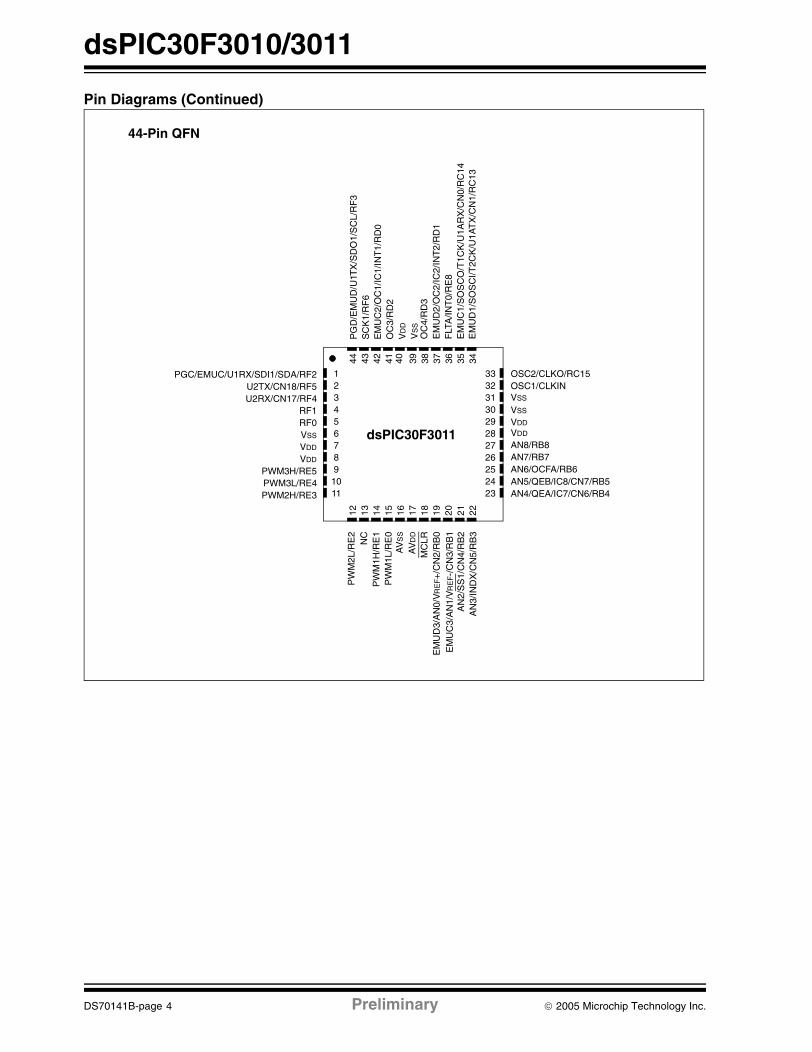
Pin Diagrams (Continued)
44-Pin QFN
44 43 42 41 40 39 38 37 36 35
14 15 16 17 18 19 20 21
33029282726252423
45
7891011
12 32
31
dsPIC30F3011
PWM2H/RE3PWM3L/RE4PWM3H/RE5
VDD
VDD
RF0RF1
U2RX/CN17/RF4U2TX/CN18/RF5
PGC/EMUC/U1RX/SDI1/SDA/RF2
AN
3/IN
DX
/CN
5/R
B3
AN
2/S
S1/
CN
4/R
B2
EM
UC
3/A
N1/
VR
EF-/
CN
3/R
B1
EM
UD
3/A
N0/
VR
EF+
/CN
2/R
B0
MC
LRA
VD
D
PW
M1L
/RE
0P
WM
1H/R
E1
PW
M2L
/RE
2
AN4/QEA/IC7/CN6/RB4AN5/QEB/IC8/CN7/RB5AN6/OCFA/RB6AN7/RB7AN8/RB8
VDD
VSS
OSC1/CLKINOSC2/CLKO/RC15
PG
D/E
MU
D/U
1TX
/SD
O1/
SC
L/R
F3
SC
K1/
RF
6E
MU
C2/
OC
1/IC
1/IN
T1/
RD
0O
C3/
RD
2V
DD
EM
UC
1/S
OS
CO
/T1C
K/U
1AR
X/C
N0/
RC
14
OC
4/R
D3
EM
UD
2/O
C2/
IC2/
INT
2/R
D1
FLT
A/IN
T0/
RE
8
6
22
33
34
VSS
AV
SS
VDD
VS
S
EM
UD
1/S
OS
CI/T
2CK
/U1A
TX
/CN
1/R
C13
VSS
NC
12 13
DS70141B-page 4 Preliminary © 2005 Microchip Technology Inc.

dsPIC30F3010/3011
Pin Diagrams (Continued)
dsP
IC30
F30
10
MCLR
PWM1L/RE0PWM1H/RE1PWM2L/RE2PWM2H/RE3PWM3L/RE4PWM3H/RE5VSS
VDD
EMUD3/AN0/VREF+/CN2/RB0EMUC3/AN1/VREF-/CN3/RB1
AVDD
AVSS
AN2/SS1/CN4/RB2
EMUD2/OC2/IC2/INT2/RD1 EMUC2/OC1/IC1/INT1/RD0
EMUC1/SOSCO/T1CK/U1ARX/CN0/RC14EMUD1/SOSCI/T2CK/U1ATX/CN1/RC13
VSSOSC2/CLKO/RC15OSC1/CLKIN VDD
FLTA/INT0/SCK1/OCFA/RE8
PGC/EMUC/U1RX/SDI1/SDA/RF2PGD/EMUD/U1TX/SDO1/SCL/RF3
AN5/QEB/IC8/CN7/RB5AN4/QEA/IC7/CN6/RB4
AN3/INDX/CN5/RB3
1234567891011121314
2827262524232221201918171615
28-Pin SPDIP28-Pin SOIC
44-Pin QFN
44 43 42 41 40 39 38 37 36 35
14 15 16 17 18 19 20 21
33029282726252423
45
7891011
12 32
31
dsPIC30F3010
PWM2H/RE3PWM3L/RE4PWM3H/RE5
VDD
VDD
CRX1/RF0CTX1/RF1
U2RX/CN17/RF4U2TX/CN18/RF5
PGC/EMUC/U1RX/SDI1/SDA/RF2
AN
3/IN
DX
/CN
5/R
B3
AN
2/S
S1/
CN
4/R
B2
EM
UC
3/A
N1/
VR
EF-/
CN
3/R
B1
EM
UD
3/A
N0/
VR
EF+
/CN
2/R
B0
MC
LRA
VD
D
PW
M1L
/RE
0P
WM
1H/R
E1
PW
M2L
/RE
2
AN4/QEA/IC7/CN6/RB4AN5/QEB/IC8/CN7/RB5NCNCNC
VDD
VSS
OSC1/CLKINOSC2/CLKO/RC15
PG
D/E
MU
D/U
1TX
/SD
O1/
SC
L/R
F3
SC
K1/
RF
6E
MU
C2/
OC
1/IC
1/IN
T1/
RD
0O
C3/
RD
2V
DD
EM
UC
1/S
OS
CO
/T1C
K/U
1AR
X/C
N0/
RC
14
OC
4/R
D3
EM
UD
2/O
C2/
IC2/
INT
2/R
D1
FLT
A/IN
T0/
RE
8
6
22
33
34
VSS
AV
SS
VDD
VS
S
EM
UD
1/S
OS
CI/T
2CK
/U1A
TX
/CN
1/R
C13
VSS
NC
12 13
© 2005 Microchip Technology Inc. Preliminary DS70141B-page 5

dsPIC30F3010/3011
Table of Contents
1.0 Device Overview ...................................................................................................................................................................... 72.0 CPU Architecture Overview.................................................................................................................................................... 153.0 Memory Organization ............................................................................................................................................................. 234.0 Address Generator Units........................................................................................................................................................ 355.0 Interrupts ................................................................................................................................................................................ 416.0 Flash Program Memory.......................................................................................................................................................... 477.0 Data EEPROM Memory ......................................................................................................................................................... 538.0 I/O Ports ................................................................................................................................................................................. 579.0 Timer1 Module ....................................................................................................................................................................... 6310.0 Timer2/3 Module .................................................................................................................................................................... 6711.0 Timer4/5 Module ................................................................................................................................................................... 7312.0 Input Capture Module............................................................................................................................................................. 7713.0 Output Compare Module ........................................................................................................................................................ 8114.0 Quadrature Encoder Interface (QEI) Module ......................................................................................................................... 8515.0 Motor Control PWM Module ................................................................................................................................................... 9116.0 SPI™ Module ....................................................................................................................................................................... 10117.0 I2C Module ........................................................................................................................................................................... 10518.0 Universal Asynchronous Receiver Transmitter (UART) Module .......................................................................................... 11319.0 10-bit High Speed Analog-to-Digital Converter (A/D) Module .............................................................................................. 12120.0 System Integration ............................................................................................................................................................... 12921.0 Instruction Set Summary ...................................................................................................................................................... 14322.0 Development Support........................................................................................................................................................... 15123.0 Electrical Characteristics ...................................................................................................................................................... 15724.0 Packaging Information.......................................................................................................................................................... 199The Microchip Web Site ..................................................................................................................................................................... 213Customer Change Notification Service .............................................................................................................................................. 213Customer Support .............................................................................................................................................................................. 213Reader Response .............................................................................................................................................................................. 214Product Identification System............................................................................................................................................................. 215
TO OUR VALUED CUSTOMERS
It is our intention to provide our valued customers with the best documentation possible to ensure successful use of your Microchipproducts. To this end, we will continue to improve our publications to better suit your needs. Our publications will be refined andenhanced as new volumes and updates are introduced.
If you have any questions or comments regarding this publication, please contact the Marketing Communications Department viaE-mail at [email protected] or fax the Reader Response Form in the back of this data sheet to (480) 792-4150. Wewelcome your feedback.
Most Current Data SheetTo obtain the most up-to-date version of this data sheet, please register at our Worldwide Web site at:
http://www.microchip.com
You can determine the version of a data sheet by examining its literature number found on the bottom outside corner of any page.The last character of the literature number is the version number, (e.g., DS30000A is version A of document DS30000).
ErrataAn errata sheet, describing minor operational differences from the data sheet and recommended workarounds, may exist for currentdevices. As device/documentation issues become known to us, we will publish an errata sheet. The errata will specify the revisionof silicon and revision of document to which it applies.
To determine if an errata sheet exists for a particular device, please check with one of the following:
• Microchip’s Worldwide Web site; http://www.microchip.com• Your local Microchip sales office (see last page)When contacting a sales office, please specify which device, revision of silicon and data sheet (include literature number) you areusing.
Customer Notification SystemRegister on our web site at www.microchip.com to receive the most current information on all of our products.
DS70141B-page 6 Preliminary © 2005 Microchip Technology Inc.

dsPIC30F3010/3011
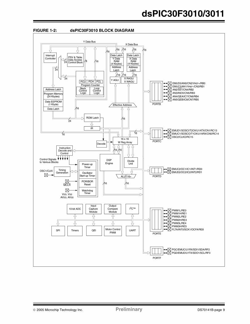
1.0 DEVICE OVERVIEW This document contains device specific information forthe dsPIC30F3010/3011 device. The dsPIC30Fdevices contain extensive Digital Signal Processor(DSP) functionality within a high performance 16-bitmicrocontroller (MCU) architecture. Figure 1-1 andFigure 1-2 show device block diagrams for thedsPIC30F3011 and dsPIC30F3010 devices.
Note: This data sheet summarizes features of this groupof dsPIC30F devices and is not intended to be a completereference source. For more information on the CPU,peripherals, register descriptions and general devicefunctionality, refer to the dsPIC30F Family ReferenceManual (DS70046). For more information on the deviceinstruction set and programming, refer to the dsPIC30FProgrammer’s Reference Manual (DS70030).
© 2005 Microchip Technology Inc. Preliminary DS70141B-page 7

dsPIC30F3010/3011
FIGURE 1-1: dsPIC30F3011 BLOCK DIAGRAM
AN8/RB8
Power-upTimer
OscillatorStart-up Timer
POR/BORReset
WatchdogTimer
InstructionDecode and
Control
OSC1/CLKI
MCLR
VDD, VSS
AN4/QEA/IC7/CN6/RB4
UART1,SPI Motor ControlPWM
TimingGeneration
AN5/QEB/IC8/CN7/RB5
16
PCH PCLProgram Counter
ALU<16>
16
Address Latch
Program Memory(24 Kbytes)
Data Latch
24
24
24
24
X Data Bus
IR
I2C™
QEI
AN6/OCFA/RB6AN7/RB7
PCU
PWM1L/RE0PWM1H/RE1PWM2L/RE2PWM2H/RE3PWM3L/RE4
10-bit ADC
Timers
PWM3H/RE5FLTA/INT0/RE8
U2TX/CN18/RF5SCK1/RF6
InputCaptureModule
Output Compare
Module
EMUC1/SOSCO/T1CK/U1ARX/CN0/RC14EMUD1/SOSCI/T2CK/U1ATX/CN1/RC13
PORTB
RF0RF1PGC/EMUC/U1RX/SDI1/SDA/RF2PGD/EMUD/U1TX/SDO1/SCL/RF3
PORTF
PORTD
16
16 16
16 x 16W Reg Array
Divide UnitEngine
DSP
Decode
ROM Latch
16
Y Data Bus
Effective Address
X RAGUX WAGU Y AGU
EMUD3/AN0/VREF+/CN2/RB0EMUC3/AN1/VREF-/CN3/RB1AN2/SS1/CN4/RB2AN3/INDX/CN5/RB3
OSC2/CLKO/RC15
U2RX/CN17/RF4
AVDD, AVSS
UART2
16
16
16
16
16
PORTC
PORTE
16
16
16
16
8
InterruptController PSV & Table
Data AccessControl Block
StackControl Logic
LoopControlLogic
Data LatchData LatchY Data
(4 Kbytes)RAM
X Data
(4 Kbytes)RAM
AddressLatch
AddressLatch
Control Signals to Various Blocks
EMUC2/OC1/IC1/INT1/RD0EMUD2/OC2/IC2/INT2/RD1OC3/RD2OC4/RD3
16
Data EEPROM(1 Kbyte)
16
DS70141B-page 8 Preliminary © 2005 Microchip Technology Inc.
dsPIC30F3010/3011
FIGURE 1-2: dsPIC30F3010 BLOCK DIAGRAM
InstructionDecode and
Control
OSC1/CLKI
MCLR
VDD, VSS
AN4/QEA/IC7/CN6/RB4
UARTSPI Motor ControlPWM
TimingGeneration
AN5/QEB/IC8/CN7/RB5
16
PCH PCLProgram Counter
ALU<16>
16
Address Latch
Program Memory(24 Kbytes)
Data Latch
24
24
24
24
X Data Bus
IR
I2C™
QEI
PCU
PWM1L/RE0PWM1H/RE1PWM2L/RE2PWM2H/RE3PWM3L/RE4
10-bit ADC
Timers
PWM3H/RE5FLTA/INT0/SCK1/OCFA/RE8
InputCaptureModule
Output Compare
Module
EMUC1/SOSCO/T1CK/U1ARX/CN0/RC14EMUD1/SOSCI/T2CK/U1ATX/CN1/RC13
PORTB
PGC/EMUC/U1RX/SDI1/SDA/RF2PGD/EMUD/U1TX/SDO1/SCL/RF3
PORTF
PORTD
16
16 16
16 x 16W Reg Array
Divide Unit Engine
DSP
Decode
ROM Latch
16
Y Data Bus
Effective Address
X RAGUX WAGU Y AGU
EMUD3/AN0/CN2/VREF+/RB0EMUC3/AN1/VREF-/CN3/RB1AN2/SS1/CN4/RB2AN3/INDX/CN5/RB3
OSC2/CLKO/RC15
AVDD, AVSS
16
16
16
16
16
PORTC
PORTE
16
16
16
16
8
InterruptController PSV & Table
Data AccessControl Block
StackControl Logic
LoopControlLogic
Data LatchData LatchY Data
(4 Kbytes)RAM
X Data
(4 Kbytes)RAM
AddressLatch
AddressLatch
Control Signals to Various Blocks
EMUC2/OC1/IC1/INT1/RD0EMUD2/OC2/IC2/INT2/RD1
16
Data EEPROM(1 Kbyte)
16
Power-upTimer
OscillatorStart-up Timer
POR/BORReset
WatchdogTimer
© 2005 Microchip Technology Inc. Preliminary DS70141B-page 9

dsPIC30F3010/3011
Table 1-1 provides a brief description of the device I/Opinout and the functions that are multiplexed to a portpin. Multiple functions may exist on one port pin. Whenmultiplexing occurs, the peripheral module’s functionalrequirements may force an override of the datadirection of the port pin.
TABLE 1-1: dsPIC30F3011 I/O PIN DESCRIPTIONS
Pin NamePin
TypeBuffer Type
Description
AN0-AN8 I Analog Analog input channels. AN0 and AN1 are also used for device programming data and clock inputs, respectively.
AVDD P P Positive supply for analog module.
AVSS P P Ground reference for analog module.
CLKINCLKO
IO
ST/CMOS—
External clock source input. Always associated with OSC1 pin function.Oscillator crystal output. Connects to crystal or resonator in Crystal Oscillator mode. Optionally functions as CLKO in RC and EC modes.Always associated with OSC2 pin function.
CN0-CN7CN17-CN18
I ST Input change notification inputs.Can be software programmed for internal weak pull-ups on all inputs.
EMUDEMUCEMUD1EMUC1EMUD2EMUC2EMUD3EMUC3
I/OI/OI/OI/OI/OI/OI/OI/O
STSTSTSTSTSTSTST
ICD Primary Communication Channel data input/output pin.ICD Primary Communication Channel clock input/output pin.ICD Secondary Communication Channel data input/output pin.ICD Secondary Communication Channel clock input/output pin.ICD Tertiary Communication Channel data input/output pin.ICD Tertiary Communication Channel clock input/output pin.ICD Quaternary Communication Channel data input/output pin.ICD Quaternary Communication Channel clock input/output pin.
IC1, IC2, IC7, IC8
I ST Capture inputs 1, 2, 7 and 8.
INDXQEA
QEB
II
I
STST
ST
Quadrature Encoder Index Pulse input.Quadrature Encoder Phase A input in QEI mode. Auxiliary Timer External Clock/Gate input in Timer mode.Quadrature Encoder Phase A input in QEI mode. Auxiliary Timer External Clock/Gate input in Timer mode.
INT0INT1INT2
III
STSTST
External interrupt 0.External interrupt 1.External interrupt 2.
FLTAPWM1LPWM1HPWM2LPWM2HPWM3LPWM3H
IOOOOOO
ST——————
PWM Fault A input.PWM 1 Low output. PWM 1 High output.PWM 2 Low output.PWM 2 High output.PWM 3 Low output.PWM 3 High output.
MCLR I/P ST Master Clear (Reset) input or programming voltage input. This pin is an active low Reset to the device.
OCFAOC1-OC4
IO
ST—
Compare Fault A input (for Compare channels 1, 2, 3 and 4).Compare outputs 1 through 4.
Legend: CMOS = CMOS compatible input or output Analog = Analog inputST = Schmitt Trigger input with CMOS levels O = Output I = Input P = Power
DS70141B-page 10 Preliminary © 2005 Microchip Technology Inc.

dsPIC30F3010/3011
OSC1OSC2
II/O
ST/CMOS—
Oscillator crystal input. ST buffer when configured in RC mode; CMOS otherwise.Oscillator crystal output. Connects to crystal or resonator in Crystal Oscillator mode. Optionally functions as CLKO in RC and EC modes.
PGDPGC
I/OI
STST
In-Circuit Serial Programming™ data input/output pin.In-Circuit Serial Programming clock input pin.
RB0-RB8 I/O ST PORTB is a bidirectional I/O port.
RC13-RC15 I/O ST PORTC is a bidirectional I/O port.
RD0-RD3 I/O ST PORTD is a bidirectional I/O port.
RE0-RE5, RE8
I/O ST PORTE is a bidirectional I/O port.
RF0-RF6 I/O ST PORTF is a bidirectional I/O port.
SCK1SDI1SDO1SS1
I/OIOI
STST—ST
Synchronous serial clock input/output for SPI™ #1.SPI #1 Data In.SPI #1 Data Out.SPI #1 Slave Synchronization.
SCLSDA
I/OI/O
STST
Synchronous serial clock input/output for I2C.Synchronous serial data input/output for I2C.
SOSCOSOSCI
OI
—ST/CMOS
32 kHz low power oscillator crystal output. 32 kHz low power oscillator crystal input. ST buffer when configured in RC mode; CMOS otherwise.
T1CKT2CK
II
STST
Timer1 external clock input.Timer2 external clock input.
U1RXU1TXU1ARXU1ATXU2RXU2TX
IOIOIO
ST—ST—ST—
UART1 Receive.UART1 Transmit.UART1 Alternate Receive.UART1 Alternate Transmit.UART2 Receive.UART2 Transmit.
VDD P — Positive supply for logic and I/O pins.
VSS P — Ground reference for logic and I/O pins.
VREF+ I Analog Analog Voltage Reference (High) input.
VREF- I Analog Analog Voltage Reference (Low) input.
TABLE 1-1: dsPIC30F3011 I/O PIN DESCRIPTIONS (CONTINUED)
Pin NamePin
TypeBuffer Type
Description
Legend: CMOS = CMOS compatible input or output Analog = Analog inputST = Schmitt Trigger input with CMOS levels O = Output I = Input P = Power
© 2005 Microchip Technology Inc. Preliminary DS70141B-page 11

dsPIC30F3010/3011
Table 1-2 provides a brief description of the device I/Opinout and the functions that are multiplexed to a portpin. Multiple functions may exist on one port pin. Whenmultiplexing occurs, the peripheral module’s functionalrequirements may force an override of the datadirection of the port pin.
TABLE 1-2: dsPIC30F3010 I/O PIN DESCRIPTIONS
Pin NamePin
TypeBuffer Type
Description
AN0-AN5 I Analog Analog input channels. AN0 and AN1 are also used for device programming data and clock inputs, respectively.
AVDD P P Positive supply for analog module.
AVSS P P Ground reference for analog module.
CLKINCLKO
IO
ST/CMOS—
External clock source input. Always associated with OSC1 pin function.Oscillator crystal output. Connects to crystal or resonator in Crystal Oscillator mode. Optionally functions as CLKO in RC and EC modes.Always associated with OSC2 pin function.
CN0-CN7 I ST Input change notification inputs.Can be software programmed for internal weak pull-ups on all inputs.
EMUDEMUCEMUD1EMUC1EMUD2EMUC2EMUD3EMUC3
I/OI/OI/OI/OI/OI/OI/OI/O
STSTSTSTSTSTSTST
ICD Primary Communication Channel data input/output pin.ICD Primary Communication Channel clock input/output pin.ICD Secondary Communication Channel data input/output pin.ICD Secondary Communication Channel clock input/output pin.ICD Tertiary Communication Channel data input/output pin.ICD Tertiary Communication Channel clock input/output pin.ICD Quaternary Communication Channel data input/output pin.ICD Quaternary Communication Channel clock input/output pin.
IC1, IC2, IC7, IC8
I ST Capture inputs 1, 2, 7 and 8.
INDXQEA
QEB
II
I
STST
ST
Quadrature Encoder Index Pulse input.Quadrature Encoder Phase A input in QEI mode. Auxiliary Timer External Clock/Gate input in Timer mode.Quadrature Encoder Phase A input in QEI mode. Auxiliary Timer External Clock/Gate input in Timer mode.
INT0INT1INT2
III
STSTST
External interrupt 0.External interrupt 1.External interrupt 2.
FLTAPWM1LPWM1HPWM2LPWM2HPWM3LPWM3H
IOOOOOO
ST——————
PWM Fault A input.PWM 1 Low output. PWM 1 High output.PWM 2 Low output.PWM 2 High output.PWM 3 Low output.PWM 3 High output.
MCLR I/P ST Master Clear (Reset) input or programming voltage input. This pin is an active low Reset to the device.
OCFAOC1, OC2
IO
ST—
Compare Fault A input (for Compare channels 1, 2, 3 and 4).Compare outputs 1 and 2.
Legend: CMOS = CMOS compatible input or output Analog = Analog inputST = Schmitt Trigger input with CMOS levels O = Output I = Input P = Power
DS70141B-page 12 Preliminary © 2005 Microchip Technology Inc.

dsPIC30F3010/3011
OSC1OSC2
II/O
ST/CMOS—
Oscillator crystal input. ST buffer when configured in RC mode; CMOS otherwise.Oscillator crystal output. Connects to crystal or resonator in Crystal Oscillator mode. Optionally functions as CLKO in RC and EC modes.
PGDPGC
I/OI
STST
In-Circuit Serial Programming™ data input/output pin.In-Circuit Serial Programming clock input pin.
RB0-RB5 I/O ST PORTB is a bidirectional I/O port.
RC13-RC15 8I/O 8ST PORTC is a bidirectional I/O port.
RD0-RD1 I/O ST PORTD is a bidirectional I/O port.
RE0-RE5, RE8
I/O ST PORTE is a bidirectional I/O port.
RF2-RF3 I/O ST PORTF is a bidirectional I/O port.
SCK1SDI1SDO1
I/OIO
STST—
Synchronous serial clock input/output for SPI #1.SPI #1 Data In.SPI #1 Data Out.
SCLSDA
I/OI/O
STST
Synchronous serial clock input/output for I2C™.Synchronous serial data input/output for I2C.
SOSCOSOSCI
OI
—ST/CMOS
32 kHz low power oscillator crystal output. 32 kHz low power oscillator crystal input. ST buffer when configured in RC mode; CMOS otherwise.
T1CKT2CK
II
STST
Timer1 external clock input.Timer2 external clock input.
U1RXU1TXU1ARXU1ATX
IOIO
ST—ST—
UART1 Receive.UART1 Transmit.UART1 Alternate Receive.UART1 Alternate Transmit.
VDD P — Positive supply for logic and I/O pins.
VSS P — Ground reference for logic and I/O pins.
VREF+ I Analog Analog Voltage Reference (High) input.
VREF- I Analog Analog Voltage Reference (Low) input.
TABLE 1-2: dsPIC30F3010 I/O PIN DESCRIPTIONS (CONTINUED)
Pin NamePin
TypeBuffer Type
Description
Legend: CMOS = CMOS compatible input or output Analog = Analog inputST = Schmitt Trigger input with CMOS levels O = Output I = Input P = Power
© 2005 Microchip Technology Inc. Preliminary DS70141B-page 13

dsPIC30F3010/3011
NOTES:
DS70141B-page 14 Preliminary © 2005 Microchip Technology Inc.

dsPIC30F3010/3011
2.0 CPU ARCHITECTURE OVERVIEW
2.1 Core Overview
The core has a 24-bit instruction word. The ProgramCounter (PC) is 23 bits wide with the Least Significant(LS) bit always clear (see Section 3.1), and the MostSignificant (MS) bit is ignored during normal programexecution, except for certain specialized instructions.Thus, the PC can address up to 4M instruction wordsof user program space. An instruction pre-fetch mech-anism is used to help maintain throughput. Programloop constructs, free from loop count managementoverhead, are supported using the DO and REPEATinstructions, both of which are interruptible at any point.
The working register array consists of 16x16-bit regis-ters, each of which can act as Data, Address or Offsetregisters. One working register (W15) operates as asoftware Stack Pointer (SP) for interrupts and calls.
The data space is 64 Kbytes (32K words) and is splitinto two blocks, referred to as X and Y data memory.Each block has its own independent Address Genera-tion Unit (AGU). Most instructions operate solelythrough the X memory AGU, which provides theappearance of a single unified data space. TheMultiply-Accumulate (MAC) class of dual source DSPinstructions operate through both the X and Y AGUs,splitting the data address space into two parts (seeSection 3.2 "Data Address Space"). The X and Ydata space boundary is device specific and cannot bealtered by the user. Each data word consists of 2 bytes,and most instructions can address data either as wordsor bytes.
There are two methods of accessing data stored inprogram memory:
• The upper 32 Kbytes of data space memory can be mapped into the lower half (user space) of pro-gram space at any 16K program word boundary, defined by the 8-bit Program Space Visibility Page (PSVPAG) register. This lets any instruction access program space as if it were data space, with a limitation that the access requires an addi-tional cycle. Moreover, only the lower 16 bits of each instruction word can be accessed using this method.
• Linear indirect access of 32K word pages within program space is also possible using any working register, via table read and write instructions. Table read and write instructions can be used to access all 24 bits of an instruction word.
Overhead-free circular buffers (modulo addressing) aresupported in both X and Y address spaces. This isprimarily intended to remove the loop overhead forDSP algorithms.
The X AGU also supports bit-reversed addressing ondestination effective addresses, to greatly simplify inputor output data reordering for radix-2 FFT algorithms.Refer to Section 4.0 "Address Generator Units" fordetails on modulo and bit-reversed addressing.
The core supports Inherent (no operand), Relative, Lit-eral, Memory Direct, Register Direct, Register Indirect,Register Offset and Literal Offset Addressing modes.Instructions are associated with predefined Addressingmodes, depending upon their functional requirements.
For most instructions, the core is capable of executinga data (or program data) memory read, a working reg-ister (data) read, a data memory write and a program(instruction) memory read per instruction cycle. As aresult, 3 operand instructions are supported, allowingC = A+B operations to be executed in a single cycle.
A DSP engine has been included to significantlyenhance the core arithmetic capability and throughput.It features a high speed 17-bit by 17-bit multiplier, a40-bit ALU, two 40-bit saturating accumulators and a40-bit bi-directional barrel shifter. Data in the accumu-lator or any working register can be shifted up to 16 bitsright or 16 bits left in a single cycle. The DSP instruc-tions operate seamlessly with all other instructions andhave been designed for optimal real-time performance.The MAC class of instructions can concurrently fetchtwo data operands from memory, while multiplying twoW registers. To enable this concurrent fetching of dataoperands, the data space has been split for theseinstructions and linear for all others. This has beenachieved in a transparent and flexible manner, bydedicating certain working registers to each addressspace for the MAC class of instructions.
The core does not support a multi-stage instructionpipeline. However, a single stage instruction pre-fetchmechanism is used, which accesses and partiallydecodes instructions a cycle ahead of execution, inorder to maximize available execution time. Mostinstructions execute in a single cycle, with certainexceptions.
The core features a vectored exception processingstructure for traps and interrupts, with 62 independentvectors. The exceptions consist of up to 8 traps (ofwhich 4 are reserved) and 54 interrupts. Each interruptis prioritized based on a user assigned priority between1 and 7 (1 being the lowest priority and 7 being thehighest) in conjunction with a predetermined ‘naturalorder’. Traps have fixed priorities, ranging from 8 to 15.
Note: This data sheet summarizes features of this groupof dsPIC30F devices and is not intended to be a completereference source. For more information on the CPU,peripherals, register descriptions and general devicefunctionality, refer to the dsPIC30F Family ReferenceManual (DS70046). For more information on the deviceinstruction set and programming, refer to the dsPIC30FProgrammer’s Reference Manual (DS70030).
© 2005 Microchip Technology Inc. Preliminary DS70141B-page 15

dsPIC30F3010/3011
2.2 Programmer’s Model
The programmer’s model is shown in Figure 2-1 andconsists of 16x16-bit working registers (W0 throughW15), 2x40-bit accumulators (AccA and AccB), StatusRegister (SR), Data Table Page register (TBLPAG),Program Space Visibility Page register (PSVPAG), DOand REPEAT registers (DOSTART, DOEND, DCOUNTand RCOUNT) and Program Counter (PC). The work-ing registers can act as Data, Address or Offset regis-ters. All registers are memory mapped. W0 acts as theW register for file register addressing.
Some of these registers have a Shadow register asso-ciated with each of them, as shown in Figure 2-1. TheShadow register is used as a temporary holding regis-ter and can transfer its contents to or from its host reg-ister upon the occurrence of an event. None of theShadow registers are accessible directly. The followingrules apply for transfer of registers into and out ofshadows.
• PUSH.S and POP.S W0, W1, W2, W3, SR (DC, N, OV, Z and C bits only) are transferred.
• DO instruction DOSTART, DOEND, DCOUNT shadows are pushed on loop start, and popped on loop end.
When a byte operation is performed on a working reg-ister, only the Least Significant Byte of the target regis-ter is affected. However, a benefit of memory mappedworking registers is that both the Least and MostSignificant Bytes can be manipulated through bytewide data memory space accesses.
2.2.1 SOFTWARE STACK POINTER/ FRAME POINTER
The dsPIC® DSC devices contain a software stack.W15 is the dedicated software Stack Pointer, and willbe automatically modified by exception processing andsubroutine calls and returns. However, W15 can be ref-erenced by any instruction in the same manner as allother W registers. This simplifies the reading, writingand manipulation of the Stack Pointer (e.g., creatingstack frames).
W15 is initialized to 0x0800 during a Reset. The usermay reprogram the SP during initialization to anylocation within data space.
W14 has been dedicated as a Stack Frame Pointer asdefined by the LNK and ULNK instructions. However,W14 can be referenced by any instruction in the samemanner as all other W registers.
2.2.2 STATUS REGISTER
The dsPIC DSC core has a 16-bit Status Register (SR),the LS Byte of which is referred to as the SR Low Byte(SRL) and the MS Byte as the SR High Byte (SRH).See Figure 2-1 for SR layout.
SRL contains all the MCU ALU operation status flags(including the Z bit), as well as the CPU Interrupt Prior-ity Level status bits, IPL<2:0>, and the REPEAT activestatus bit, RA. During exception processing, SRL isconcatenated with the MS Byte of the PC to form acomplete word value which is then stacked.
The upper byte of the SR register contains the DSPAdder/Subtractor status bits, the DO Loop Active bit(DA) and the Digit Carry (DC) status bit.
2.2.3 PROGRAM COUNTER
The Program Counter is 23 bits wide. Bit 0 is alwaysclear. Therefore, the PC can address up to 4Minstruction words.
Note: In order to protect against misalignedstack accesses, W15<0> is always clear.
DS70141B-page 16 Preliminary © 2005 Microchip Technology Inc.

dsPIC30F3010/3011
FIGURE 2-1: PROGRAMMER’S MODEL
TABPAG
PC22 PC0
7 0
D0D15
Program Counter
Data Table Page Address
Status Register
Working Registers
DSP OperandRegisters
W1
W2
W3
W4
W5
W6
W7
W8
W9
W10
W11
W12/DSP Offset
W13/DSP Write Back
W14/Frame Pointer
W15/Stack Pointer
DSP AddressRegisters
AD39 AD0AD31
DSPAccumulators
AccA
AccB
PSVPAG0
Program Space Visibility Page Address
Z
0
OA OB SA SB
RCOUNT15 0
REPEAT Loop Counter
DCOUNT15 0
DO Loop Counter
DOSTART
22 0DO Loop Start Address
IPL2 IPL1
SPLIM Stack Pointer Limit Register
AD15
SRL
PUSH.S Shadow
DO Shadow
OAB SAB
15 0 Core Configuration Register
Legend
CORCON
DA DC RA N
TBLPAG
PSVPAG
IPL0 OV
W0/WREG
SRH
DO Loop End AddressDOEND
22
C
7
© 2005 Microchip Technology Inc. Preliminary DS70141B-page 17

dsPIC30F3010/3011
2.3 Divide Support
The dsPIC DSC devices feature a 16/16-bit signedfractional divide operation, as well as 32/16-bit and 16/16-bit signed and unsigned integer divide operations, inthe form of single instruction iterative divides. The fol-lowing instructions and data sizes are supported:
1. DIVF – 16/16 signed fractional divide2. DIV.sd – 32/16 signed divide
3. DIV.ud – 32/16 unsigned divide4. DIV.sw – 16/16 signed divide5. DIV.uw – 16/16 unsigned divide
The divide instructions must be executed within aREPEAT loop. Any other form of execution (e.g. a seriesof discrete divide instructions) will not function correctlybecause the instruction flow depends on RCOUNT. Thedivide instruction does not automatically set up theRCOUNT value, and it must, therefore, be explicitly andcorrectly specified in the REPEAT instruction, as shownin Table 2-1 (REPEAT will execute the target instruction{operand value+1} times). The REPEAT loop count mustbe set up for 18 iterations of the DIV/DIVF instruction.Thus, a complete divide operation requires 19 cycles.
TABLE 2-1: DIVIDE INSTRUCTIONS
2.4 DSP Engine
The DSP engine consists of a high speed 17-bit x17-bit multiplier, a barrel shifter, and a 40-bit adder/subtractor (with two target accumulators, round andsaturation logic).
The dsPIC30F devices have a single instruction flowwhich can execute either DSP or MCU instructions.Many of the hardware resources are shared betweenthe DSP and MCU instructions. For example, theinstruction set has both DSP and MCU multiplyinstructions which use the same hardware multiplier.
The DSP engine also has the capability to performinherent accumulator-to-accumulator operations, whichrequire no additional data. These instructions are ADD,SUB and NEG.
The DSP engine has various options selected throughvarious bits in the CPU Core Configuration register(CORCON), as listed below:
1. Fractional or integer DSP multiply (IF).2. Signed or unsigned DSP multiply (US).
3. Conventional or convergent rounding (RND).4. Automatic saturation on/off for AccA (SATA).5. Automatic saturation on/off for AccB (SATB).
6. Automatic saturation on/off for writes to datamemory (SATDW).
7. Accumulator Saturation mode selection(ACCSAT).
A block diagram of the DSP engine is shown inFigure 2-2.
Note: The divide flow is interruptible. However,the user needs to save the context asappropriate.
Instruction Function
DIVF Signed fractional divide: Wm/Wn → W0; Rem → W1
DIV.sd Signed divide: (Wm+1:Wm)/Wn → W0; Rem → W1
DIV.sw (or DIV.s) Signed divide: Wm/Wn → W0; Rem → W1
DIV.ud Unsigned divide: (Wm+1:Wm)/Wn → W0; Rem → W1
DIV.uw (or DIV.u) Unsigned divide: Wm/Wn → W0; Rem → W1
TABLE 2-2: DSP INSTRUCTION SUMMARY
Instruction Algebraic Operation
CLR A = 0
ED A = (x – y)2
EDAC A = A + (x – y)2
MAC A = A + (x * y)
MOVSAC No change in A
MPY A = x * y
MPY.N A = – x * y
MSC A = A – x * y
DS70141B-page 18 Preliminary © 2005 Microchip Technology Inc.

dsPIC30F3010/3011
FIGURE 2-2: DSP ENGINE BLOCK DIAGRAM
Zero Backfill
Sign-Extend
BarrelShifter
40-bit Accumulator A40-bit Accumulator B
RoundLogic
X D
ata
Bus
To/From W Array
Adder
Saturate
Negate
32
3233
16
16 16
16
4040
40 40
Saturate
Y D
ata
Bus
40
Carry/Borrow Out
Carry/Borrow In
16
40
Multiplier/Scaler17-bit
© 2005 Microchip Technology Inc. Preliminary DS70141B-page 19

dsPIC30F3010/3011
2.4.1 MULTIPLIER
The 17x17-bit multiplier is capable of signed orunsigned operation and can multiplex its output using ascaler to support either 1.31 fractional (Q31) or 32-bitinteger results. Unsigned operands are zero-extendedinto the 17th bit of the multiplier input value. Signedoperands are sign-extended into the 17th bit of themultiplier input value. The output of the 17x17-bitmultiplier/scaler is a 33-bit value, which is sign-extended to 40 bits. Integer data is inherentlyrepresented as a signed two’s complement value,where the MSB is defined as a sign bit. Generallyspeaking, the range of an N-bit two’s complementinteger is -2N-1 to 2N-1 – 1. For a 16-bit integer, the datarange is -32768 (0x8000) to 32767 (0x7FFF), including0. For a 32-bit integer, the data range is -2,147,483,648(0x8000 0000) to 2,147,483,645 (0x7FFF FFFF).
When the multiplier is configured for fractional multipli-cation, the data is represented as a two’s complementfraction, where the MSB is defined as a sign bit and theradix point is implied to lie just after the sign bit(QX format). The range of an N-bit two’s complementfraction with this implied radix point is -1.0 to (1-21-N).For a 16-bit fraction, the Q15 data range is -1.0(0x8000) to 0.999969482 (0x7FFF), including 0 andhas a precision of 3.01518x10⁻⁵. In fractional mode, a16x16 multiply operation generates a 1.31 product,which has a precision of 4.65661x10⁻¹⁰.
The same multiplier is used to support the MCUmultiply instructions, which include integer 16-bitsigned, unsigned and mixed sign multiplies.
The MUL instruction may be directed to use byte orword-sized operands. Byte operands will direct a 16-bitresult, and word operands will direct a 32-bit result tothe specified register(s) in the W array.
2.4.2 DATA ACCUMULATORS AND ADDER/SUBTRACTOR
The data accumulator consists of a 40-bit adder/subtractor with automatic sign extension logic. It canselect one of two accumulators (A or B) as its pre-accumulation source and post-accumulation destina-tion. For the ADD and LAC instructions, the data to beaccumulated or loaded can be optionally scaled via thebarrel shifter, prior to accumulation.
2.4.2.1 Adder/Subtractor, Overflow and Saturation
The adder/subtractor is a 40-bit adder with an optionalzero input into one side and either true or complementdata into the other input. In the case of addition, thecarry/borrow input is active high and the other input istrue data (not complemented), whereas in the case ofsubtraction, the carry/borrow input is active low and theother input is complemented. The adder/subtractorgenerates overflow status bits SA/SB and OA/OB,which are latched and reflected in the Status register.
• Overflow from bit 39: this is a catastrophic overflow in which the sign of the accumulator is destroyed.
• Overflow into guard bits 32 through 39: this is a recoverable overflow. This bit is set whenever all the guard bits are not identical to each other.
The adder has an additional saturation block whichcontrols accumulator data saturation, if selected. Ituses the result of the adder, the overflow status bitsdescribed above, and the SATA/B (CORCON<7:6>)and ACCSAT (CORCON<4>) mode control bits todetermine when and to what value to saturate.
Six Status register bits have been provided to supportsaturation and overflow; they are:
1. OA:AccA overflowed into guard bits
2. OB: AccB overflowed into guard bits
3. SA:AccA saturated (bit 31 overflow and saturation)orAccA overflowed into guard bits and saturated(bit 39 overflow and saturation)
4. SB:AccB saturated (bit 31 overflow and saturation)orAccB overflowed into guard bits and saturated(bit 39 overflow and saturation)
5. OAB:Logical OR of OA and OB
6. SAB:Logical OR of SA and SB
The OA and OB bits are modified each time datapasses through the adder/subtractor. When set, theyindicate that the most recent operation has overflowedinto the accumulator guard bits (bits 32 through 39).The OA and OB bits can also optionally generate anarithmetic warning trap when set and the correspond-ing overflow trap flag enable bit (OVATEN, OVBTEN) inthe INTCON1 register (refer to Section 5.0) is set. Thisallows the user to take immediate action, for example,to correct system gain.
DS70141B-page 20 Preliminary © 2005 Microchip Technology Inc.

dsPIC30F3010/3011
The SA and SB bits are modified each time data passesthrough the adder/subtractor, but can only be cleared bythe user. When set, they indicate that the accumulatorhas overflowed its maximum range (bit 31 for 32-bitsaturation, or bit 39 for 40-bit saturation) and will besaturated (if saturation is enabled). When saturation isnot enabled, SA and SB default to bit 39 overflow andthus indicate that a catastrophic overflow has occurred.If the COVTE bit in the INTCON1 register is set, SA andSB bits will generate an arithmetic warning trap whensaturation is disabled.
The overflow and saturation status bits can optionallybe viewed in the Status Register (SR) as the logical ORof OA and OB (in bit OAB) and the logical OR of SA andSB (in bit SAB). This allows programmers to check onebit in the Status register to determine if eitheraccumulator has overflowed, or one bit to determine ifeither accumulator has saturated. This would be usefulfor complex number arithmetic which typically usesboth the accumulators.
The device supports three Saturation and Overflowmodes.
1. Bit 39 Overflow and Saturation:When bit 39 overflow and saturation occurs, thesaturation logic loads the maximally positive 9.31(0x7FFFFFFFFF) or maximally negative 9.31value (0x8000000000) into the targetaccumulator. The SA or SB bit is set andremains set until cleared by the user. This isreferred to as ‘super saturation’ and providesprotection against erroneous data or unexpectedalgorithm problems (e.g., gain calculations).
2. Bit 31 Overflow and Saturation:When bit 31 overflow and saturation occurs, thesaturation logic then loads the maximallypositive 1.31 value (0x007FFFFFFF) ormaximally negative 1.31 value (0x0080000000)into the target accumulator. The SA or SB bit isset and remains set until cleared by the user.When this Saturation mode is in effect, the guardbits are not used (so the OA, OB or OAB bits arenever set).
3. Bit 39 Catastrophic OverflowThe bit 39 overflow status bit from the adder isused to set the SA or SB bit, which remain setuntil cleared by the user. No saturation operationis performed and the accumulator is allowed tooverflow (destroying its sign). If the COVTE bit inthe INTCON1 register is set, a catastrophicoverflow can initiate a trap exception.
2.4.2.2 Accumulator ‘Write Back’
The MAC class of instructions (with the exception ofMPY, MPY.N, ED and EDAC) can optionally write arounded version of the high word (bits 31 through 16)of the accumulator that is not targeted by the instructioninto data space memory. The write is performed acrossthe X bus into combined X and Y address space. Thefollowing addressing modes are supported:
1. W13, Register Direct:The rounded contents of the non-target accumula-tor are written into W13 as a 1.15 fraction.
2. [W13]+=2, Register Indirect with Post-Increment:The rounded contents of the non-target accumu-lator are written into the address pointed to byW13 as a 1.15 fraction. W13 is thenincremented by 2 (for a word write).
2.4.2.3 Round Logic
The round logic is a combinational block, which per-forms a conventional (biased) or convergent (unbiased)round function during an accumulator write (store). TheRound mode is determined by the state of the RND bitin the CORCON register. It generates a 16-bit, 1.15 datavalue which is passed to the data space write saturationlogic. If rounding is not indicated by the instruction, atruncated 1.15 data value is stored and the LS Word issimply discarded.
Conventional rounding takes bit 15 of the accumulator,zero-extends it and adds it to the ACCxH word (bits 16through 31 of the accumulator). If the ACCxL word (bits0 through 15 of the accumulator) is between 0x8000and 0xFFFF (0x8000 included), ACCxH isincremented. If ACCxL is between 0x0000 and 0x7FFF,ACCxH is left unchanged. A consequence of thisalgorithm is that over a succession of random roundingoperations, the value will tend to be biased slightlypositive.
Convergent (or unbiased) rounding operates in thesame manner as conventional rounding, except whenACCxL equals 0x8000. If this is the case, the LS bit (bit16 of the accumulator) of ACCxH is examined. If it is ‘1’,ACCxH is incremented. If it is ‘0’, ACCxH is not modi-fied. Assuming that bit 16 is effectively random innature, this scheme will remove any rounding bias thatmay accumulate.
The SAC and SAC.R instructions store either a trun-cated (SAC) or rounded (SAC.R) version of the contentsof the target accumulator to data memory, via the X bus(subject to data saturation, see Section 2.4.2.4). Notethat for the MAC class of instructions, the accumulatorwrite back operation will function in the same manner,addressing combined MCU (X and Y) data spacethough the X bus. For this class of instructions, the datais always subject to rounding.
© 2005 Microchip Technology Inc. Preliminary DS70141B-page 21

dsPIC30F3010/3011
2.4.2.4 Data Space Write Saturation
In addition to adder/subtractor saturation, writes to dataspace may also be saturated, but without affecting thecontents of the source accumulator. The data spacewrite saturation logic block accepts a 16-bit, 1.15fractional value from the round logic block as its input,together with overflow status from the original source(accumulator) and the 16-bit round adder. These arecombined and used to select the appropriate 1.15fractional value as output to write to data spacememory.
If the SATDW bit in the CORCON register is set, data(after rounding or truncation) is tested for overflow andadjusted accordingly. For input data greater than0x007FFF, data written to memory is forced to themaximum positive 1.15 value, 0x7FFF. For input dataless than 0xFF8000, data written to memory is forcedto the maximum negative 1.15 value, 0x8000. The MSbit of the source (bit 39) is used to determine the signof the operand being tested.
If the SATDW bit in the CORCON register is not set, theinput data is always passed through unmodified underall conditions.
2.4.3 BARREL SHIFTER
The barrel shifter is capable of performing up to 16-bitarithmetic or logic right shifts, or up to 16-bit left shiftsin a single cycle. The source can be either of the twoDSP accumulators or the X bus (to support multi-bitshifts of register or memory data).
The shifter requires a signed binary value to determineboth the magnitude (number of bits) and direction of theshift operation. A positive value will shift the operandright. A negative value will shift the operand left. Avalue of 0 will not modify the operand.
The barrel shifter is 40 bits wide, thereby obtaining a40-bit result for DSP shift operations and a 16-bit resultfor MCU shift operations. Data from the X bus ispresented to the barrel shifter between bit positions 16to 31 for right shifts, and bit positions 0 to 15 for leftshifts.
DS70141B-page 22 Preliminary © 2005 Microchip Technology Inc.

dsPIC30F3010/3011
3.0 MEMORY ORGANIZATION
3.1 Program Address Space
The program address space is 4M instruction words. Itis addressable by the 23-bit PC, table instructionEffective Address (EA), or data space EA, whenprogram space is mapped into data space, as definedby Table 3-1. Note that the program space address isincremented by two between successive programwords, in order to provide compatibility with data spaceaddressing.
User program space access is restricted to the lower4M instruction word address range (0x000000 to0x7FFFFE), for all accesses other than TBLRD/TBLWT,which use TBLPAG<7> to determine user or configura-tion space access. In Table 3-1, Read/Write instruc-tions, bit 23 allows access to the Device ID, the User IDand the configuration bits. Otherwise, bit 23 is alwaysclear.
FIGURE 3-1: PROGRAM SPACE MEMORY MAP FOR dsPIC30F3010/3011 Note: This data sheet summarizes features of this group
of dsPIC30F devices and is not intended to be a completereference source. For more information on the CPU,peripherals, register descriptions and general devicefunctionality, refer to the dsPIC30F Family ReferenceManual (DS70046). For more information on the deviceinstruction set and programming, refer to the dsPIC30FProgrammer’s Reference Manual (DS70030).
Reset - Target Address
Use
r M
emor
yS
pace
000000
00007E
000002
000080
Device Configuration
User FlashProgram Memory
004000003FFE
Con
figur
atio
n M
emor
yS
pace
Data EEPROM
(8K instructions)
(1 Kbyte)
800000
F80000Registers F8000E
F80010
DEVID (2)
FEFFFEFF0000FFFFFE
ReservedF7FFFE
Reserved
7FFC007FFBFE
(Read 0’s)
8005FE800600
UNITID (32 instr.)
8005BE8005C0
Reset - GOTO Instruction
000004
Reserved
7FFFFE
Reserved
0001000000FE000084Alternate Vector Table
Reserved
Interrupt Vector TableVector Tables
© 2005 Microchip Technology Inc. Preliminary DS70141B-page 23

dsPIC30F3010/3011
TABLE 3-1: PROGRAM SPACE ADDRESS CONSTRUCTION
FIGURE 3-2: DATA ACCESS FROM PROGRAM SPACE ADDRESS GENERATION
Access TypeAccessSpace
Program Space Address<23> <22:16> <15> <14:1> <0>
Instruction Access User 0 PC<22:1> 0
TBLRD/TBLWT User (TBLPAG<7> = 0)
TBLPAG<7:0> Data EA <15:0>
TBLRD/TBLWT Configuration (TBLPAG<7> = 1)
TBLPAG<7:0> Data EA <15:0>
Program Space Visibility User 0 PSVPAG<7:0> Data EA <14:0>
0Program Counter
23 bits
1
PSVPAG Reg
8 bits
EA
15 bits
Program
Using
Select
TBLPAG Reg
8 bits
EA
16 bits
Using
Byte24-bit EA
0
0
1/0
Select
User/Configuration
TableInstruction
ProgramSpace
Counter
Using
Space Select
Note: Program Space Visibility cannot be used to access bits <23:16> of a word in program memory.
Visibility
DS70141B-page 24 Preliminary © 2005 Microchip Technology Inc.

dsPIC30F3010/3011
3.1.1 DATA ACCESS FROM PROGRAM MEMORY USING TABLE INSTRUCTIONS
This architecture fetches 24-bit wide program memory.Consequently, instructions are always aligned. How-ever, as the architecture is modified Harvard, data canalso be present in program space.
There are two methods by which program space canbe accessed; via special table instructions, or throughthe remapping of a 16K word program space page intothe upper half of data space (see Section 3.1.2 "DataAccess From Program Memory Using ProgramSpace Visibility"). The TBLRDL and TBLWTL instruc-tions offer a direct method of reading or writing the LSWord of any address within program space, withoutgoing through data space. The TBLRDH and TBLWTHinstructions are the only method whereby the upper 8bits of a program space word can be accessed as data.
The PC is incremented by two for each successive24-bit program word. This allows program memoryaddresses to directly map to data space addresses.Program memory can thus be regarded as two 16-bitword wide address spaces, residing side by side, eachwith the same address range. TBLRDL and TBLWTLaccess the space which contains the LS Data Word,and TBLRDH and TBLWTH access the space whichcontains the MS Data Byte.
Figure 3-2 shows how the EA is created for table oper-ations and data space accesses (PSV = 1). Here,P<23:0> refers to a program space word, whereasD<15:0> refers to a data space word.
A set of Table Instructions are provided to move byte orword-sized data to and from program space.
1. TBLRDL: Table Read LowWord: Read the LS Word of the program address;P<15:0> maps to D<15:0>.Byte: Read one of the LS Bytes of the program address;P<7:0> maps to the destination byte when byteselect = 0;P<15:8> maps to the destination byte when byteselect = 1.
2. TBLWTL: Table Write Low (refer to Section 6.0"Flash Program Memory" for details on FlashProgramming).
3. TBLRDH: Table Read HighWord: Read the MS Word of the program address;P<23:16> maps to D<7:0>; D<15:8> always be = 0.Byte: Read one of the MS Bytes of the program address;P<23:16> maps to the destination byte whenbyte select = 0;The destination byte will always be = 0 whenbyte select = 1.
4. TBLWTH: Table Write High (refer to Section 6.0"Flash Program Memory" for details on FlashProgramming).
FIGURE 3-3: PROGRAM DATA TABLE ACCESS (LS WORD)
0816PC Address
0x0000000x000002
0x0000040x000006
2300000000
00000000
00000000
00000000
Program Memory‘Phantom’ Byte(Read as ‘0’).
TBLRDL.W
TBLRDL.B (Wn<0> = 1)
TBLRDL.B (Wn<0> = 0)
© 2005 Microchip Technology Inc. Preliminary DS70141B-page 25

dsPIC30F3010/3011
FIGURE 3-4: PROGRAM DATA TABLE ACCESS (MS BYTE)
3.1.2 DATA ACCESS FROM PROGRAM MEMORY USING PROGRAM SPACE VISIBILITY
The upper 32 Kbytes of data space may optionally bemapped into any 16K word program space page. Thisprovides transparent access of stored constant datafrom X data space, without the need to use specialinstructions (i.e., TBLRDL/H, TBLWTL/H instructions).
Program space access through the data space occursif the MS bit of the data space EA is set and programspace visibility is enabled, by setting the PSV bit in theCore Control register (CORCON). The functions ofCORCON are discussed in Section 2.4 "DSPEngine".
Data accesses to this area add an additional cycle tothe instruction being executed, since two programmemory fetches are required.
Note that the upper half of addressable data space isalways part of the X data space. Therefore, when aDSP operation uses program space mapping to accessthis memory region, Y data space should typicallycontain state (variable) data for DSP operations,whereas X data space should typically containcoefficient (constant) data.
Although each data space address, 0x8000 and higher,maps directly into a corresponding program memoryaddress (see Figure 3-5), only the lower 16-bits of the24-bit program word are used to contain the data. Theupper 8 bits should be programmed to force an illegalinstruction to maintain machine robustness. Referto the dsPIC30F Programmer’s Reference Manual(DS70030) for details on instruction encoding.
Note that by incrementing the PC by 2 for eachprogram memory word, the LS 15 bits of data spaceaddresses directly map to the LS 15 bits in thecorresponding program space addresses. Theremaining bits are provided by the Program SpaceVisibility Page register, PSVPAG<7:0>, as shown inFigure 3-5.
For instructions that use PSV which are executedoutside a REPEAT loop:
• The following instructions will require one instruc-tion cycle in addition to the specified execution time:
- MAC class of instructions with data operand pre-fetch
- MOV instructions- MOV.D instructions
• All other instructions will require two instruction cycles in addition to the specified execution time of the instruction.
For instructions that use PSV which are executedinside a REPEAT loop:
• The following instances will require two instruction cycles in addition to the specified execution time of the instruction:- Execution in the first iteration- Execution in the last iteration
- Execution prior to exiting the loop due to an interrupt
- Execution upon re-entering the loop after an interrupt is serviced
• Any other iteration of the REPEAT loop will allow the instruction, accessing data using PSV, to execute in a single cycle.
0816PC Address
0x0000000x000002
0x0000040x000006
2300000000
00000000
00000000
00000000
Program Memory‘Phantom’ Byte(Read as ‘0’)
TBLRDH.W
TBLRDH.B (Wn<0> = 1)
TBLRDH.B (Wn<0> = 0)
Note: PSV access is temporarily disabled duringTable Reads/Writes.
DS70141B-page 26 Preliminary © 2005 Microchip Technology Inc.

dsPIC30F3010/3011
FIGURE 3-5: DATA SPACE WINDOW INTO PROGRAM SPACE OPERATION
3.2 Data Address Space
The core has two data spaces. The data spaces can beconsidered either separate (for some DSP instruc-tions), or as one unified linear address range (for MCUinstructions). The data spaces are accessed using twoAddress Generation Units (AGUs) and separate datapaths.
3.2.1 DATA SPACE MEMORY MAP
The data space memory is split into two blocks, X andY data space. A key element of this architecture is thatY space is a subset of X space, and is fully containedwithin X space. In order to provide an apparent linearaddressing space, X and Y spaces have contiguousaddresses.
When executing any instruction other than one of theMAC class of instructions, the X block consists of the 64Kbyte data address space (including all Y addresses).When executing one of the MAC class of instructions,the X block consists of the 64 Kbyte data addressspace excluding the Y address block (for data readsonly). In other words, all other instructions regard theentire data memory as one composite address space.The MAC class instructions extract the Y address spacefrom data space and address it using EAs sourced fromW10 and W11. The remaining X data space isaddressed using W8 and W9. Both address spaces areconcurrently accessed only with the MAC classinstructions.
A data space memory map is shown in Figure 3-6.
Figure 3-7 shows a graphical summary of how X and Ydata spaces are accessed for MCU and DSPinstructions.
23 15 0
PSVPAG(1)15
15
EA<15> = 0
EA<15> = 1
16DataSpace
EA
Data Space Program Space
8
15 23
0x0000
0x8000
0xFFFF
0x00
0x003FFE
Data Read
Upper half of Data Space is mapped into Program Space
Note: PSVPAG is an 8-bit register, containing bits <22:15> of the program space address (i.e., it defines the page in program space to which the upper half of data space is being mapped).
0x001200AddressConcatenation
BSET CORCON,#2 ; PSV bit setMOV #0x00, W0 ; Set PSVPAG registerMOV W0, PSVPAGMOV 0x9200, W0 ; Access program memory location
; using a data space access
0x000100
© 2005 Microchip Technology Inc. Preliminary DS70141B-page 27

dsPIC30F3010/3011
FIGURE 3-6: dsPIC30F3010/3011 DATA SPACE MEMORY MAP
0x0000
0x07FE
0x09FE
0xFFFE
LS ByteAddress16 bits
LSBMSB
MS ByteAddress
0x0001
0x07FF
0x09FF
0xFFFF
0x8001 0x8000
OptionallyMappedinto ProgramMemory
0x0BFF 0xBFE
0x0C000x0C01
0x0801 0x0800
0x0A01 0x0A00
NearData
2 KbyteSFR Space
1 Kbyte
SRAM Space
3072 bytes
Space
Unimplemented (X)X Data
SFR Space
X Data RAM (X)
Y Data RAM (Y)
DS70141B-page 28 Preliminary © 2005 Microchip Technology Inc.

dsPIC30F3010/3011
FIGURE 3-7: DATA SPACE FOR MCU AND DSP (MAC CLASS) INSTRUCTIONS EXAMPLE
SFR SPACE
(Y SPACE)
X S
PA
CE
SFR SPACE
UNUSED
X S
PA
CE
X S
PA
CE
Y SPACE
UNUSED
UNUSED
Non-MAC Class Ops (Read/Write) MAC Class Ops Read Only
Indirect EA using any W Indirect EA using W8, W9 Indirect EA using W10, W11
MAC Class Ops (Write)
© 2005 Microchip Technology Inc. Preliminary DS70141B-page 29

dsPIC30F3010/3011
3.2.2 DATA SPACES
The X data space is used by all instructions and sup-ports all addressing modes. There are separate readand write data buses. The X read data bus is the returndata path for all instructions that view data space ascombined X and Y address space. It is also the Xaddress space data path for the dual operand readinstructions (MAC class). The X write data bus is theonly write path to data space for all instructions.
The X data space also supports Modulo Addressing forall instructions, subject to Addressing mode restric-tions. Bit-Reversed Addressing is only supported forwrites to X data space.
The Y data space is used in concert with the X dataspace by the MAC class of instructions (CLR, ED,EDAC, MAC, MOVSAC, MPY, MPY.N and MSC) toprovide two concurrent data read paths. No writesoccur across the Y bus. This class of instructionsdedicates two W register pointers, W10 and W11, toalways address Y data space, independent of X dataspace, whereas W8 and W9 always address X dataspace. Note that during accumulator write back, thedata address space is considered a combination of Xand Y data spaces, so the write occurs across the Xbus. Consequently, the write can be to any address inthe entire data space.
The Y data space can only be used for the data pre-fetch operation associated with the MAC class ofinstructions. It also supports Modulo Addressing forautomated circular buffers. Of course, all other instruc-tions can access the Y data address space through theX data path, as part of the composite linear space.
The boundary between the X and Y data spaces isdefined as shown in Figure 3-6 and is not user pro-grammable. Should an EA point to data outside its ownassigned address space, or to a location outside phys-ical memory, an all-zero word/byte will be returned. Forexample, although Y address space is visible by allnon-MAC instructions using any Addressing mode, anattempt by a MAC instruction to fetch data from thatspace, using W8 or W9 (X space pointers), will return0x0000.
All effective addresses are 16 bits wide and point tobytes within the data space. Therefore, the data spaceaddress range is 64 Kbytes or 32K words.
3.2.3 DATA SPACE WIDTH
The core data width is 16-bits. All internal registers areorganized as 16-bit wide words. Data space memory isorganized in byte addressable, 16-bit wide blocks.
3.2.4 DATA ALIGNMENT
To help maintain backward compatibility withPICmicro® devices and improve data space memoryusage efficiency, the dsPIC30F instruction set supportsboth word and byte operations. Data is aligned in datamemory and registers as words, but all data space EAsresolve to bytes. Data byte reads will read the completeword, which contains the byte, using the LS bit of anyEA to determine which byte to select. The selected byteis placed onto the LS Byte of the X data path (no byteaccesses are possible from the Y data path as the MACclass of instruction can only fetch words). That is, datamemory and registers are organized as two parallelbyte wide entities with shared (word) address decode,but separate write lines. Data byte writes only write tothe corresponding side of the array or register whichmatches the byte address.
As a consequence of this byte accessibility, all effectiveaddress calculations (including those generated by theDSP operations, which are restricted to word-sizeddata) are internally scaled to step through word alignedmemory. For example, the core would recognize thatPost-Modified Register Indirect Addressing mode,[Ws++], will result in a value of Ws+1 for byteoperations and Ws+2 for word operations.
All word accesses must be aligned to an even address.Misaligned word data fetches are not supported, socare must be taken when mixing byte and word opera-tions, or translating from 8-bit MCU code. Should a mis-aligned read or write be attempted, an Address Errortrap will be generated. If the error occurred on a read,the instruction underway is completed, whereas if itoccurred on a write, the instruction will be executed butthe write will not occur. In either case, a trap will thenbe executed, allowing the system and/or user to exam-ine the machine state prior to execution of the addressfault.
FIGURE 3-8: DATA ALIGNMENTTABLE 3-2: EFFECT OF INVALID MEMORY ACCESSES
Attempted Operation Data Returned
EA = an unimplemented address 0x0000
W8 or W9 used to access Y data space in a MAC instruction
0x0000
W10 or W11 used to access X data space in a MAC instruction
0x0000
15 8 7 0
0001
0003
0005
0000
0002
0004
Byte 1 Byte 0
Byte 3 Byte 2
Byte 5 Byte 4
LS ByteMS Byte
DS70141B-page 30 Preliminary © 2005 Microchip Technology Inc.

dsPIC30F3010/3011
All byte loads into any W register are loaded into theLS Byte. The MSB is not modified.
A sign-extend (SE) instruction is provided to allowusers to translate 8-bit signed data to 16-bit signedvalues. Alternatively, for 16-bit unsigned data, userscan clear the MSB of any W register by executing azero-extend (ZE) instruction on the appropriateaddress.
Although most instructions are capable of operating onword or byte data sizes, it should be noted that someinstructions, including the DSP instructions, operateonly on words.
3.2.5 NEAR DATA SPACE
An 8 Kbyte ‘near’ data space is reserved in X addressmemory space between 0x0000 and 0x1FFF, which isdirectly addressable via a 13-bit absolute address fieldwithin all memory direct instructions. The remaining Xaddress space and all of the Y address space isaddressable indirectly. Additionally, the whole of X dataspace is addressable using MOV instructions, whichsupport memory direct addressing with a 16-bitaddress field.
3.2.6 SOFTWARE STACK
The dsPIC DSC device contains a software stack. W15is used as the Stack Pointer.
The Stack Pointer always points to the first availablefree word and grows from lower addresses towardshigher addresses. It pre-decrements for stack pops andpost-increments for stack pushes, as shown inFigure 3-9. Note that for a PC push during any CALLinstruction, the MSB of the PC is zero-extended beforethe push, ensuring that the MSB is always clear.
There is a Stack Pointer Limit register (SPLIM) associ-ated with the Stack Pointer. SPLIM is uninitialized atReset. As is the case for the Stack Pointer, SPLIM<0>is forced to ‘0’, because all stack operations must beword aligned. Whenever an effective address (EA) isgenerated using W15 as a source or destinationpointer, the address thus generated is compared withthe value in SPLIM. If the contents of the Stack Pointer(W15) and the SPLIM register are equal and a pushoperation is performed, a Stack Error Trap will notoccur. The Stack Error Trap will occur on a subsequentpush operation. Thus, for example, if it is desirable tocause a Stack Error Trap when the stack grows beyondaddress 0x2000 in RAM, initialize the SPLIM with thevalue, 0x1FFE.
Similarly, a Stack Pointer Underflow (Stack Error) trapis generated when the Stack Pointer Address is foundto be less than 0x0800, thus preventing the stack frominterfering with the Special Function Register (SFR)space.
A write to the SPLIM register should not be immediatelyfollowed by an indirect read operation using W15.
FIGURE 3-9: CALL STACK FRAME
Note: A PC push during exception processingwill concatenate the SRL register to theMSB of the PC prior to the push.
<Free Word>
PC<15:0>
000000000
015
W15 (before CALL)
W15 (after CALL)
Sta
ck G
row
s To
war
dsH
ighe
r A
ddre
ss
PUSH: [W15++]POP: [--W15]
0x0000
PC<22:16>
© 2005 Microchip Technology Inc. Preliminary DS70141B-page 31
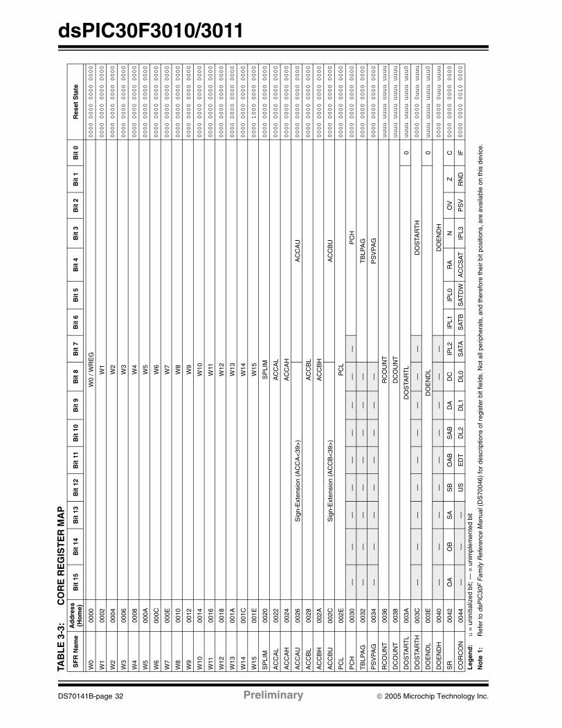
dsPIC30F3010/3011
TABL
E 3
-3:
CO
RE
RE
GIS
TE
R M
AP
SF
R N
ame
Ad
dre
ss(H
om
e)B
it 1
5B
it 1
4B
it 1
3B
it 1
2B
it 1
1B
it 1
0B
it 9
Bit
8B
it 7
Bit
6B
it 5
Bit
4B
it 3
Bit
2B
it 1
Bit
0R
eset
Sta
te
W0
0000
W0
/ WR
EG
0000 0000 0000 0000
W1
0002
W1
0000 0000 0000 0000
W2
0004
W2
0000 0000 0000 0000
W3
0006
W3
0000 0000 0000 0000
W4
0008
W4
0000 0000 0000 0000
W5
000A
W5
0000 0000 0000 0000
W6
000C
W6
0000 0000 0000 0000
W7
000E
W7
0000 0000 0000 0000
W8
0010
W8
0000 0000 0000 0000
W9
0012
W9
0000 0000 0000 0000
W10
0014
W10
0000 0000 0000 0000
W11
0016
W11
0000 0000 0000 0000
W12
0018
W12
0000 0000 0000 0000
W13
001A
W13
0000 0000 0000 0000
W14
001C
W14
0000 0000 0000 0000
W15
001E
W15
0000 1000 0000 0000
SP
LIM
0020
SP
LIM
0000 0000 0000 0000
AC
CA
L00
22A
CC
AL
0000 0000 0000 0000
AC
CA
H00
24A
CC
AH
0000 0000 0000 0000
AC
CA
U00
26S
ign-
Ext
ensi
on (
AC
CA
<39
>)
AC
CA
U0000 0000 0000 0000
AC
CB
L00
28A
CC
BL
0000 0000 0000 0000
AC
CB
H00
2AA
CC
BH
0000 0000 0000 0000
AC
CB
U00
2CS
ign-
Ext
ensi
on (
AC
CB
<39
>)
AC
CB
U0000 0000 0000 0000
PC
L00
2EP
CL
0000 0000 0000 0000
PC
H00
30—
——
——
——
——
PC
H0000 0000 0000 0000
TB
LPA
G00
32—
——
——
——
—T
BLP
AG
0000 0000 0000 0000
PS
VP
AG
0034
——
——
——
——
PS
VP
AG
0000 0000 0000 0000
RC
OU
NT
0036
RC
OU
NT
uuuu uuuu uuuu uuuu
DC
OU
NT
0038
DC
OU
NT
uuuu uuuu uuuu uuuu
DO
STA
RT
L00
3AD
OS
TAR
TL
0uuuu uuuu uuuu uuu0
DO
STA
RT
H00
3C—
——
——
——
——
DO
STA
RT
H0000 0000 0uuu uuuu
DO
EN
DL
003E
DO
EN
DL
0uuuu uuuu uuuu uuu0
DO
EN
DH
0040
——
——
——
——
—D
OE
ND
H0000 0000 0uuu uuuu
SR
0042
OA
OB
SA
SB
OA
BS
AB
DA
DC
IPL2
IPL1
IPL0
RA
NO
VZ
C0000 0000 0000 0000
CO
RC
ON
0044
——
—U
SE
DT
DL2
DL1
DL0
SA
TAS
AT
BS
AT
DW
AC
CS
AT
IPL3
PS
VR
ND
IF0000 0000 0010 0000
Leg
end
:u
= u
nini
tializ
ed b
it; —
= u
nim
plem
ente
d bi
t
No
te1:
Ref
er to
dsP
IC30
F F
amily
Ref
eren
ce M
anua
l (D
S70
046)
for
desc
riptio
ns o
f reg
iste
r bi
t fie
lds.
Not
all
perip
hera
ls, a
nd th
eref
ore
thei
r bi
t pos
ition
s, a
re a
vaila
ble
on th
is d
evic
e.
DS70141B-page 32 Preliminary © 2005 Microchip Technology Inc.

dsPIC30F3010/3011
MO
DC
ON
0046
XM
OD
EN
YM
OD
EN
——
BW
M<
3:0>
YW
M<
3:0>
XW
M<
3:0>
0000 0000 0000 0000
XM
OD
SR
T00
48X
S<
15:1
>0
uuuu uuuu uuuu uuu0
XM
OD
EN
D00
4AX
E<
15:1
>1
uuuu uuuu uuuu uuu1
YM
OD
SR
T00
4CY
S<
15:1
>0
uuuu uuuu uuuu uuu0
YM
OD
EN
D00
4EY
E<
15:1
>1
uuuu uuuu uuuu uuu1
XB
RE
V00
50B
RE
NX
B<
14:0
>uuuu uuuu uuuu uuuu
DIS
ICN
T00
52—
—D
ISIC
NT
<13
:0>
0000 0000 0000 0000
TAB
LE
3-3
:C
OR
E R
EG
IST
ER
MA
P (
CO
NT
INU
ED
)
SF
R N
ame
Ad
dre
ss(H
om
e)B
it 1
5B
it 1
4B
it 1
3B
it 1
2B
it 1
1B
it 1
0B
it 9
Bit
8B
it 7
Bit
6B
it 5
Bit
4B
it 3
Bit
2B
it 1
Bit
0R
eset
Sta
te
Leg
end
:u
= u
nini
tializ
ed b
it; —
= u
nim
plem
ente
d bi
t
No
te1:
Ref
er to
dsP
IC30
F F
amily
Ref
eren
ce M
anua
l (D
S70
046)
for
desc
riptio
ns o
f reg
iste
r bi
t fie
lds.
Not
all
perip
hera
ls, a
nd th
eref
ore
thei
r bi
t pos
ition
s, a
re a
vaila
ble
on th
is d
evic
e.
© 2005 Microchip Technology Inc. Preliminary DS70141B-page 33

dsPIC30F3010/3011
NOTES:
DS70141B-page 34 Preliminary © 2005 Microchip Technology Inc.

dsPIC30F3010/3011
4.0 ADDRESS GENERATOR UNITS
The dsPIC core contains two independent addressgenerator units: the X AGU and Y AGU. The Y AGUsupports word-sized data reads for the DSP MAC classof instructions only. The dsPIC AGUs support threetypes of data addressing:
• Linear Addressing
• Modulo (Circular) Addressing• Bit-Reversed Addressing
Linear and Modulo Data Addressing modes can beapplied to data space or program space. Bit-Reversedaddressing is only applicable to data space addresses.
4.1 Instruction Addressing Modes
The addressing modes in Table 4-1 form the basis ofthe addressing modes optimized to support the specificfeatures of individual instructions. The addressingmodes provided in the MAC class of instructions aresomewhat different from those in the other instructiontypes.
4.1.1 FILE REGISTER INSTRUCTIONS
Most file register instructions use a 13-bit address field(f) to directly address data present in the first 8192bytes of data memory (near data space). Most fileregister instructions employ a working register W0,which is denoted as WREG in these instructions. Thedestination is typically either the same file register, orWREG (with the exception of the MUL instruction),which writes the result to a register or register pair. TheMOV instruction allows additional flexibility and canaccess the entire data space during file registeroperation.
4.1.2 MCU INSTRUCTIONS
The three-operand MCU instructions are of the form:
Operand 3 = Operand 1 <function> Operand 2
where Operand 1 is always a working register (i.e., theaddressing mode can only be register direct), which isreferred to as Wb. Operand 2 can be a W register,fetched from data memory, or a 5-bit literal. The resultlocation can be either a W register or an addresslocation. The following addressing modes aresupported by MCU instructions:
• Register Direct• Register Indirect
• Register Indirect Post-modified• Register Indirect Pre-modified• 5-bit or 10-bit Literal
TABLE 4-1: FUNDAMENTAL ADDRESSING MODES SUPPORTED
Note: This data sheet summarizes features of this groupof dsPIC30F devices and is not intended to be a completereference source. For more information on the CPU,peripherals, register descriptions and general devicefunctionality, refer to the dsPIC30F Family ReferenceManual (DS70046). For more information on the deviceinstruction set and programming, refer to the dsPIC30FProgrammer’s Reference Manual (DS70030).
Note: Not all instructions support all the address-ing modes given above. Individualinstructions may support different subsetsof these addressing modes.
Addressing Mode Description
File Register Direct The address of the file register is specified explicitly.
Register Direct The contents of a register are accessed directly.
Register Indirect The contents of Wn forms the EA.
Register Indirect Post-modified The contents of Wn forms the EA. Wn is post-modified (incremented or decremented) by a constant value.
Register Indirect Pre-modified Wn is pre-modified (incremented or decremented) by a signed constant value to form the EA.
Register Indirect with Register Offset The sum of Wn and Wb forms the EA.
Register Indirect with Literal Offset The sum of Wn and a literal forms the EA.
© 2005 Microchip Technology Inc. Preliminary DS70141B-page 35

dsPIC30F3010/3011
4.1.3 MOVE AND ACCUMULATOR INSTRUCTIONS
Move instructions and the DSP Accumulator class ofinstructions provide a greater degree of addressingflexibility than other instructions. In addition to theaddressing modes supported by most MCU instruc-tions, Move and Accumulator instructions also supportRegister Indirect with Register Offset Addressingmode, also referred to as Register Indexed mode.
In summary, the following addressing modes aresupported by Move and Accumulator instructions:
• Register Direct• Register Indirect• Register Indirect Post-modified
• Register Indirect Pre-modified• Register Indirect with Register Offset (Indexed)• Register Indirect with Literal Offset
• 8-bit Literal• 16-bit Literal
4.1.4 MAC INSTRUCTIONS
The dual source operand DSP instructions (CLR, ED,EDAC, MAC, MPY, MPY.N, MOVSAC and MSC), alsoreferred to as MAC instructions, utilize a simplified set ofaddressing modes to allow the user to effectivelymanipulate the data pointers through register indirecttables.
The two source operand pre-fetch registers must be amember of the set {W8, W9, W10, W11}. For datareads, W8 and W9 will always be directed to the XRAGU and W10 and W11 will always be directed to theY AGU. The effective addresses generated (before andafter modification) must, therefore, be valid addresseswithin X data space for W8 and W9 and Y data spacefor W10 and W11.
In summary, the following addressing modes aresupported by the MAC class of instructions:
• Register Indirect• Register Indirect Post-modified by 2• Register Indirect Post-modified by 4
• Register Indirect Post-modified by 6• Register Indirect with Register Offset (Indexed)
4.1.5 OTHER INSTRUCTIONS
Besides the various addressing modes outlined above,some instructions use literal constants of various sizes.For example, BRA (branch) instructions use 16-bitsigned literals to specify the branch destination directly,whereas the DISI instruction uses a 14-bit unsignedliteral field. In some instructions, such as ADD Acc, thesource of an operand or result is implied by the opcodeitself. Certain operations, such as NOP, do not have anyoperands.
4.2 Modulo Addressing
Modulo addressing is a method of providing an auto-mated means to support circular data buffers usinghardware. The objective is to remove the need for soft-ware to perform data address boundary checks whenexecuting tightly looped code, as is typical in manyDSP algorithms.
Modulo addressing can operate in either data orprogram space (since the data pointer mechanism isessentially the same for both). One circular buffer can besupported in each of the X (which also provides thepointers into Program space) and Y data spaces.Modulo addressing can operate on any W registerpointer. However, it is not advisable to use W14 or W15for Modulo addressing, since these two registers areused as the Stack Frame Pointer and Stack Pointer,respectively.
In general, any particular circular buffer can only beconfigured to operate in one direction, as there arecertain restrictions on the buffer start address (forincrementing buffers) or end address (for decrementingbuffers) based upon the direction of the buffer.
The only exception to the usage restrictions is forbuffers which have a power-of-2 length. As thesebuffers satisfy the start and end address criteria, theymay operate in a Bi-directional mode, (i.e., addressboundary checks will be performed on both the lowerand upper address boundaries).
Note: For the MOV instructions, the addressingmode specified in the instruction can differfor the source and destination EA. How-ever, the 4-bit Wb (Register Offset) field isshared between both source anddestination (but typically only used byone).
Note: Not all instructions support all the address-ing modes given above. Individualinstructions may support different subsetsof these addressing modes.
Note: Register Indirect with Register OffsetAddressing is only available for W9 (in Xspace) and W11 (in Y space).
DS70141B-page 36 Preliminary © 2005 Microchip Technology Inc.

dsPIC30F3010/3011
4.2.1 START AND END ADDRESS
The Modulo addressing scheme requires that astarting and an end address be specified and loadedinto the 16-bit Modulo Buffer Address registers:XMODSRT, XMODEND, YMODSRT and YMODEND(see Table 3-3).
The length of a circular buffer is not directly specified. Itis determined by the difference between thecorresponding start and end addresses. The maximumpossible length of the circular buffer is 32K words(64 Kbytes).
4.2.2 W ADDRESS REGISTER SELECTION
The Modulo and Bit-Reversed Addressing Controlregister MODCON<15:0> contains enable flags, aswell as a W register field to specify the W addressregisters. The XWM and YWM fields select whichregisters will operate with modulo addressing. If XWM= 15, X RAGU and X WAGU modulo addressing aredisabled. Similarly, if YWM = 15, Y AGU moduloaddressing is disabled.
The X Address Space Pointer W register (XWM), towhich modulo addressing is to be applied, is stored inMODCON<3:0> (see Table 3-3). Modulo addressing isenabled for X data space when XWM is set to any valueother than 15 and the XMODEN bit is set atMODCON<15>.
The Y Address Space Pointer W register (YWM), towhich modulo addressing is to be applied, is stored inMODCON<7:4>. Modulo addressing is enabled for Ydata space when YWM is set to any value other than 15and the YMODEN bit is set at MODCON<14>.
FIGURE 4-1: MODULO ADDRESSING OPERATION EXAMPLE
Note: Y-space modulo addressing EA calcula-tions assume word-sized data (LS bit ofevery EA is always clear).
0x1100
0x1163
Start Addr = 0x1100End Addr = 0x1163Length = 0x0032 words
ByteAddress MOV #0x1100,W0
MOV W0, XMODSRT ;set modulo start addressMOV #0x1163,W0MOV W0,MODEND ;set modulo end addressMOV #0x8001,W0MOV W0,MODCON ;enable W1, X AGU for moduloMOV #0x0000,W0 ;W0 holds buffer fill valueMOV #0x1110,W1 ;point W1 to bufferDO AGAIN,#0x31 ;fill the 50 buffer locationsMOV W0, [W1++] ;fill the next locationAGAIN: INC W0,W0 ;increment the fill value
© 2005 Microchip Technology Inc. Preliminary DS70141B-page 37
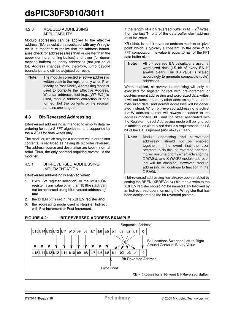
dsPIC30F3010/3011
4.2.3 MODULO ADDRESSING APPLICABILITY
Modulo addressing can be applied to the effectiveaddress (EA) calculation associated with any W regis-ter. It is important to realize that the address bound-aries check for addresses less than or greater than theupper (for incrementing buffers) and lower (for decre-menting buffers) boundary addresses (not just equalto). Address changes may, therefore, jump beyondboundaries and still be adjusted correctly.
4.3 Bit-Reversed Addressing
Bit-reversed addressing is intended to simplify data re-ordering for radix-2 FFT algorithms. It is supported bythe X AGU for data writes only.
The modifier, which may be a constant value or registercontents, is regarded as having its bit order reversed.The address source and destination are kept in normalorder. Thus, the only operand requiring reversal is themodifier.
4.3.1 BIT-REVERSED ADDRESSING IMPLEMENTATION
Bit-reversed addressing is enabled when:
1. BWM (W register selection) in the MODCONregister is any value other than 15 (the stack cannot be accessed using bit-reversed addressing)and
2. the BREN bit is set in the XBREV register and3. the addressing mode used is Register Indirect
with Pre-Increment or Post-Increment.
If the length of a bit-reversed buffer is M = 2N bytes,then the last ‘N’ bits of the data buffer start addressmust be zeros.
XB<14:0> is the bit-reversed address modifier or ‘pivotpoint’ which is typically a constant. In the case of anFFT computation, its value is equal to half of the FFTdata buffer size.
When enabled, bit-reversed addressing will only beexecuted for register indirect with pre-increment orpost-increment addressing and word-sized data writes.It will not function for any other addressing mode or forbyte-sized data, and normal addresses will be gener-ated instead. When bit-reversed addressing is active,the W address pointer will always be added to theaddress modifier (XB) and the offset associated withthe Register Indirect Addressing mode will be ignored.In addition, as word-sized data is a requirement, the LSbit of the EA is ignored (and always clear).
If bit-reversed addressing has already been enabled bysetting the BREN (XBREV<15>) bit, then a write to theXBREV register should not be immediately followed byan indirect read operation using the W register that hasbeen designated as the bit-reversed pointer.
FIGURE 4-2: BIT-REVERSED ADDRESS EXAMPLE
Note: The modulo corrected effective address iswritten back to the register only when Pre-Modify or Post-Modify Addressing mode isused to compute the Effective Address.When an address offset (e.g., [W7+W2]) isused, modulo address correction is per-formed, but the contents of the registerremains unchanged.
Note: All bit-reversed EA calculations assumeword-sized data (LS bit of every EA isalways clear). The XB value is scaledaccordingly to generate compatible (byte)addresses.
Note: Modulo addressing and bit-reversedaddressing should not be enabledtogether. In the event that the userattempts to do this, bit-reversed address-ing will assume priority when active for theX WAGU, and X WAGU modulo address-ing will be disabled. However, moduloaddressing will continue to function in theX RAGU.
b3 b2 b1 0
b2 b3 b4 0
Bit Locations Swapped Left-to-RightAround Center of Binary Value
Bit-Reversed Address
XB = 0x0008 for a 16-word Bit-Reversed Buffer
b7 b6 b5 b1
b7 b6 b5 b4b11 b10 b9 b8
b11 b10 b9 b8
b15 b14 b13 b12
b15 b14 b13 b12
Sequential Address
Pivot Point
DS70141B-page 38 Preliminary © 2005 Microchip Technology Inc.

dsPIC30F3010/3011
TABLE 4-2: BIT-REVERSED ADDRESS SEQUENCE (16-ENTRY)
TABLE 4-3: BIT-REVERSED ADDRESS MODIFIER VALUES FOR XBREV REGISTER
NormalAddress
Bit-Reversed Address
A3 A2 A1 A0 Decimal A3 A2 A1 A0 Decimal
0 0 0 0 0 0 0 0 0 0
0 0 0 1 1 1 0 0 0 8
0 0 1 0 2 0 1 0 0 4
0 0 1 1 3 1 1 0 0 12
0 1 0 0 4 0 0 1 0 2
0 1 0 1 5 1 0 1 0 10
0 1 1 0 6 0 1 1 0 6
0 1 1 1 7 1 1 1 0 14
1 0 0 0 8 0 0 0 1 1
1 0 0 1 9 1 0 0 1 9
1 0 1 0 10 0 1 0 1 5
1 0 1 1 11 1 1 0 1 13
1 1 0 0 12 0 0 1 1 3
1 1 0 1 13 1 0 1 1 11
1 1 1 0 14 0 1 1 1 7
1 1 1 1 15 1 1 1 1 15
Buffer Size (Words) XB<14:0> Bit-Reversed Address Modifier Value
512 0x0100
256 0x0080
128 0x0040
64 0x0020
32 0x0010
16 0x0008
8 0x0004
4 0x0002
2 0x0001
© 2005 Microchip Technology Inc. Preliminary DS70141B-page 39

dsPIC30F3010/3011
NOTES:
DS70141B-page 40 Preliminary © 2005 Microchip Technology Inc.

dsPIC30F3010/3011
5.0 INTERRUPTS
The dsPIC30F3010/3011 has 29 interrupt sources and4 processor exceptions (traps), which must bearbitrated based on a priority scheme.
The CPU is responsible for reading the InterruptVector Table (IVT) and transferring the address con-tained in the interrupt vector to the program counter.The interrupt vector is transferred from the programdata bus into the program counter, via a 24-bit widemultiplexer on the input of the program counter.
The Interrupt Vector Table (IVT) and AlternateInterrupt Vector Table (AIVT) are placed near thebeginning of program memory (0x000004). The IVTand AIVT are shown in Figure 5-1.
The interrupt controller is responsible for pre-processing the interrupts and processor exceptions,prior to their being presented to the processor core.The peripheral interrupts and traps are enabled,prioritized and controlled using centralized SpecialFunction Registers (SFR):
• IFS0<15:0>, IFS1<15:0>, IFS2<15:0>All interrupt request flags are maintained in these three registers. The flags are set by their respec-tive peripherals or external signals, and they are cleared via software.
• IEC0<15:0>, IEC1<15:0>, IEC2<15:0>All Interrupt Enable Control bits are maintained in these three registers. These control bits are used to individually enable interrupts from the peripherals or external signals.
• IPC0<15:0>... IPC11<7:0>The user assignable priority level associated with each of these interrupts is held centrally in these twelve registers.
• IPL<3:0> The current CPU priority level is explicitly stored in the IPL bits. IPL<3> is present in the CORCON register, whereas IPL<2:0> are present in the Status Register (SR) in the processor core.
• INTCON1<15:0>, INTCON2<15:0>Global interrupt control functions are derived from these two registers. INTCON1 contains the control and status flags for the processor exceptions. The INTCON2 register controls the external interrupt request signal behavior and the use of the alternate vector table.
All interrupt sources can be user assigned to one of 7priority levels, 1 through 7, via the IPCx registers.Each interrupt source is associated with an interruptvector, as shown in Table 5-1. Levels 7 and 1 repre-sent the highest and lowest maskable priorities,respectively.
If the NSTDIS bit (INTCON1<15>) is set, nesting ofinterrupts is prevented. Thus, if an interrupt is currentlybeing serviced, processing of a new interrupt isprevented, even if the new interrupt is of higher prioritythan the one currently being serviced.
Certain interrupts have specialized control bits for fea-tures like edge or level triggered interrupts, interrupt-on-change, etc. Control of these features remainswithin the peripheral module which generates theinterrupt.
The DISI instruction can be used to disable theprocessing of interrupts of priorities 6 and lower for acertain number of instructions, during which the DISI bit(INTCON2<14>) remains set.
When an interrupt is serviced, the PC is loaded with theaddress stored in the vector location in ProgramMemory that corresponds to the interrupt. There are 63different vectors within the IVT (refer to Figure 5-2).These vectors are contained in locations 0x000004through 0x0000FE of program memory (refer toFigure 5-2). These locations contain 24-bit addresses,and in order to preserve robustness, an address errortrap will take place should the PC attempt to fetch anyof these words during normal execution. This preventsexecution of random data as a result of accidentallydecrementing a PC into vector space, accidentallymapping a data space address into vector space, or thePC rolling over to 0x000000 after reaching the end ofimplemented program memory space. Execution of aGOTO instruction to this vector space will also generatean address error trap.
Note: This data sheet summarizes features of this groupof dsPIC30F devices and is not intended to be a completereference source. For more information on the CPU,peripherals, register descriptions and general devicefunctionality, refer to the dsPIC30F Family ReferenceManual (DS70046). For more information on the deviceinstruction set and programming, refer to the dsPIC30FProgrammer’s Reference Manual (DS70030). Note: Interrupt Flag bits get set when an
interrupt condition occurs, regardless ofthe state of its corresponding Enable bit.User software should ensure theappropriate Interrupt Flag bits are clearprior to enabling an interrupt.
Note: Assigning a priority level of 0 to aninterrupt source is equivalent to disablingthat interrupt.
Note: The IPL bits become read-only wheneverthe NSTDIS bit has been set to ‘1’.
© 2005 Microchip Technology Inc. Preliminary DS70141B-page 41

dsPIC30F3010/3011
5.1 Interrupt Priority
The user assignable Interrupt Priority (IP<2:0>) bits foreach individual interrupt source are located in the LS3-bits of each nibble, within the IPCx register(s). Bit 3of each nibble is not used and is read as a ‘0’. Thesebits define the priority level assigned to a particularinterrupt by the user.
Since more than one interrupt request source may beassigned to a specific user specified priority level, ameans is provided to assign priority within a given level.This method is called “Natural Order Priority”.
Natural Order Priority is determined by the position ofan interrupt in the vector table, and only affectsinterrupt operation when multiple interrupts with thesame user-assigned priority become pending at thesame time.
Table 5-1 lists the interrupt numbers and interruptsources for the dsPIC DSC devices and their associ-ated vector numbers.
The ability for the user to assign every interrupt to oneof seven priority levels implies that the user can assigna very high overall priority level to an interrupt with alow natural order priority. For example, the PWM FaultA Interrupt can be given a priority of 7. The INT0(external interrupt 0) may be assigned to priority level1, thus giving it a very low effective priority.
TABLE 5-1: INTERRUPT VECTOR TABLE
Note: The user selectable priority levels start at0, as the lowest priority, and level 7, as thehighest priority.
Note 1: The natural order priority scheme has 0 as the highestpriority and 53 as the lowest priority.
2: The natural order priority number is thesame as the INT number.
INT Number
Vector Number
Interrupt Source
Highest Natural Order Priority0 8 INT0 - External Interrupt 01 9 IC1 - Input Capture 12 10 OC1 - Output Compare 13 11 T1 - Timer 14 12 IC2 - Input Capture 25 13 OC2 - Output Compare 26 14 T2 - Timer 27 15 T3 - Timer 38 16 SPI #1 9 17 U1RX - UART1 Receiver
10 18 U1TX - UART1 Transmitter11 19 ADC - ADC Convert Done12 20 NVM - NVM Write Complete13 21 SI2C - I2C™ Slave Interrupt14 22 MI2C - I2C Master Interrupt15 23 Input Change Interrupt16 24 INT1 - External Interrupt 117 25 IC7 - Input Capture 718 26 IC8 - Input Capture 819 27 OC3 - Output Compare 3*20 28 OC4 - Output Compare 4*21 29 T4 - Timer 422 30 T5 - Timer 523 31 INT2 - External Interrupt 224 32 U2RX - UART2 Receiver*25 33 U2TX - UART2 Transmitter*26 34 Reserved27 35 Reserved28 36 Reserved29 37 Reserved30 38 Reserved31 39 Reserved32 40 Reserved33 41 Reserved34 42 Reserved35 43 Reserved36 44 Reserved37 45 Reserved38 46 Reserved39 47 PWM - PWM Period Match40 48 QEI - QEI Interrupt41 49 Reserved42 50 Reserved43 51 FLTA - PWM Fault A44 52 Reserved
45-53 53-61 ReservedLowest Natural Order Priority* Available on dsPIC30F3011 only
DS70141B-page 42 Preliminary © 2005 Microchip Technology Inc.

dsPIC30F3010/3011
5.2 Reset Sequence
A Reset is not a true exception, because the interruptcontroller is not involved in the Reset process. Theprocessor initializes its registers in response to aReset, which forces the PC to zero. The processor thenbegins program execution at location 0x000000. AGOTO instruction is stored in the first program memorylocation, immediately followed by the address target forthe GOTO instruction. The processor executes the GOTOto the specified address and then begins operation atthe specified target (start) address.
5.2.1 RESET SOURCES
There are 6 sources of error which will cause a devicereset.
• Watchdog Time-out:The watchdog has timed out, indicating that the processor is no longer executing the correct flow of code.
• Uninitialized W Register Trap:An attempt to use an uninitialized W register as an address pointer will cause a Reset.
• Illegal Instruction Trap:Attempted execution of any unused opcodes will result in an illegal instruction trap. Note that a fetch of an illegal instruction does not result in an illegal instruction trap if that instruction is flushed prior to execution due to a flow change.
• Brown-out Reset (BOR):A momentary dip in the power supply to the device has been detected, which may result in malfunction.
• Trap Lockout:Occurrence of multiple trap conditions simulta-neously will cause a Reset.
5.3 Traps
Traps can be considered as non-maskable interruptsindicating a software or hardware error, which adhereto a predefined priority as shown in Figure 5-1. Theyare intended to provide the user a means to correcterroneous operation during debug and when operatingwithin the application.
Note that many of these trap conditions can only bedetected when they occur. Consequently, the question-able instruction is allowed to complete prior to trapexception processing. If the user chooses to recoverfrom the error, the result of the erroneous action thatcaused the trap may have to be corrected.
There are 8 fixed priority levels for traps: Level 8through Level 15, which implies that the IPL3 is alwaysset during processing of a trap.
If the user is not currently executing a trap, and he setsthe IPL<3:0> bits to a value of ‘0111’ (Level 7), then allinterrupts are disabled, but traps can still be processed.
5.3.1 TRAP SOURCES
The following traps are provided with increasingpriority. However, since all traps can be nested, priorityhas little effect.
Math Error Trap:
The Math Error trap executes under the following threecircumstances:
1. Should an attempt be made to divide by zero,the divide operation will be aborted on a cycleboundary and the trap taken.
2. If enabled, a Math Error trap will be taken whenan arithmetic operation on either accumulator Aor B causes an overflow from bit 31 and theAccumulator Guard bits are not utilized.
3. If enabled, a Math Error trap will be taken whenan arithmetic operation on either accumulator Aor B causes a catastrophic overflow from bit 39and all saturation is disabled.
4. If the shift amount specified in a shift instructionis greater than the maximum allowed shiftamount, a trap will occur.
Note: If the user does not intend to take correc-tive action in the event of a trap errorcondition, these vectors must be loadedwith the address of a default handler thatsimply contains the RESET instruction. If,on the other hand, one of the vectorscontaining an invalid address is called, anaddress error trap is generated.
© 2005 Microchip Technology Inc. Preliminary DS70141B-page 43

dsPIC30F3010/3011
Address Error Trap:
This trap is initiated when any of the followingcircumstances occurs:
1. A misaligned data word access is attempted.2. A data fetch from our unimplemented data
memory location is attempted.3. A data access of an unimplemented program
memory location is attempted.4. An instruction fetch from vector space is
attempted.
5. Execution of a “BRA #literal” instruction or a“GOTO #literal” instruction, where literalis an unimplemented program memory address.
6. Executing instructions after modifying the PC topoint to unimplemented program memoryaddresses. The PC may be modified by loadinga value into the stack and executing a RETURNinstruction.
Stack Error Trap:
This trap is initiated under the following conditions:
1. The Stack Pointer is loaded with a value whichis greater than the (user programmable) limitvalue written into the SPLIM register (stackoverflow).
2. The Stack Pointer is loaded with a value whichis less than 0x0800 (simple stack underflow).
Oscillator Fail Trap:
This trap is initiated if the external oscillator fails andoperation becomes reliant on an internal RC backup.
5.3.2 HARD AND SOFT TRAPS
It is possible that multiple traps can become activewithin the same cycle (e.g., a misaligned word stackwrite to an overflowed address). In such a case, thefixed priority shown in Figure 5-2 is implemented,which may require the user to check if other traps arepending, in order to completely correct the fault.
‘Soft’ traps include exceptions of priority level 8 throughlevel 11, inclusive. The Arithmetic Error trap (level 11)falls into this category of traps.
‘Hard’ traps include exceptions of priority level 12through level 15, inclusive. The Address Error (level12), Stack Error (level 13) and Oscillator Error (level 14)traps fall into this category.
Each hard trap that occurs must be acknowledgedbefore code execution of any type may continue. If alower priority hard trap occurs while a higher prioritytrap is pending, acknowledged, or is being processed,a hard trap conflict will occur.
The device is automatically Reset in a hard trap conflictcondition. The TRAPR status bit (RCON<15>) is setwhen the Reset occurs, so that the condition may bedetected in software.
FIGURE 5-1: TRAP VECTORS
Note: In the MAC class of instructions, whereinthe data space is split into X and Y dataspace, unimplemented X space includesall of Y space, and unimplemented Yspace includes all of X space.
Address Error Trap Vector
Oscillator Fail Trap VectorStack Error Trap Vector
Reserved VectorMath Error Trap Vector
Reserved
Oscillator Fail Trap VectorAddress Error Trap Vector
Reserved VectorReserved VectorInterrupt 0 VectorInterrupt 1 Vector
———
Interrupt 52 VectorInterrupt 53 Vector
Math Error Trap Vector
Dec
reas
ing
Prio
rity
0x000000
0x000014
Reserved
Stack Error Trap Vector
Reserved VectorReserved VectorInterrupt 0 VectorInterrupt 1 Vector
———
Interrupt 52 VectorInterrupt 53 Vector
IVT
AIVT
0x0000800x00007E
0x0000FE
Reserved
0x000094
Reset - GOTO InstructionReset - GOTO Address 0x000002
Reserved0x0000820x000084
0x000004
Reserved Vector
DS70141B-page 44 Preliminary © 2005 Microchip Technology Inc.

dsPIC30F3010/3011
5.4 Interrupt Sequence
All interrupt event flags are sampled in the beginning ofeach instruction cycle by the IFSx registers. A pendinginterrupt request (IRQ) is indicated by the flag bit beingequal to a ‘1’ in an IFSx register. The IRQ will cause aninterrupt to occur if the corresponding bit in the interruptenable (IECx) register is set. For the remainder of theinstruction cycle, the priorities of all pending interruptrequests are evaluated.
If there is a pending IRQ with a priority level greaterthan the current processor priority level in the IPL bits,the processor will be interrupted.
The processor then stacks the current program counterand the low byte of the processor Status register (SRL),as shown in Figure 5-2. The low byte of the Status reg-ister contains the processor priority level at the time,prior to the beginning of the interrupt cycle. The proces-sor then loads the priority level for this interrupt into theStatus register. This action will disable all lower priorityinterrupts until the completion of the Interrupt ServiceRoutine (ISR).
FIGURE 5-2: INTERRUPT STACK FRAME
The RETFIE (Return from Interrupt) instruction willunstack the program counter and Status registers toreturn the processor to its state prior to the interruptsequence.
5.5 Alternate Vector TableIn Program Memory, the Interrupt Vector Table (IVT) isfollowed by the Alternate Interrupt Vector Table (AIVT),as shown in Figure 5-1. Access to the Alternate VectorTable is provided by the ALTIVT bit in the INTCON2register. If the ALTIVT bit is set, all interrupt andexception processes use the alternate vectors insteadof the default vectors. The alternate vectors areorganized the same as the default vectors. The AIVTsupports emulation and debugging efforts by providinga means to switch between an application and asupport environment without requiring the interruptvectors to be reprogrammed. This feature also enablesswitching between applications for evaluation ofdifferent software algorithms at run time.
If the AIVT is not required, the program memoryallocated to the AIVT may be used for other purposes.AIVT is not a protected section and may be freelyprogrammed by the user.
5.6 Fast Context SavingA context saving option is available using Shadowregisters. Shadow registers are provided for the DC, N,OV, Z and C bits in SR, and the registers W0 throughW3. The shadows are only one level deep. TheShadow registers are accessible using the PUSH.Sand POP.S instructions only. When the processorvectors to an interrupt, the PUSH.S instruction can beused to store the current value of the aforementionedregisters into their respective Shadow registers.
If an ISR of a certain priority uses the PUSH.S andPOP.S instructions for fast context saving, then ahigher priority ISR should not include the sameinstructions. Users must save the key registers insoftware during a lower priority interrupt, if the higherpriority ISR uses fast context saving.
5.7 External Interrupt RequestsThe dsPIC30F3010/3011 interrupt controller supportsthree external interrupt request signals, INT0-INT2.These inputs are edge sensitive; they require a low-to-high or a high-to-low transition to generate an interruptrequest. The INTCON2 register has five bits, INT0EP-INT4EP, that select the polarity of the edge detectioncircuitry.
5.8 Wake-up from Sleep and IdleThe interrupt controller may be used to wake up theprocessor from either Sleep or Idle modes, if Sleep orIdle mode is active when the interrupt is generated.
If an enabled interrupt request of sufficient priority isreceived by the interrupt controller, then the standardinterrupt request is presented to the processor. At thesame time, the processor will wake-up from Sleep orIdle and begin execution of the Interrupt ServiceRoutine needed to process the interrupt request.
Note1: The user can always lower the priority levelby writing a new value into SR. The InterruptService Routine must clear the interrupt flagbits in the IFSx register before lowering theprocessor interrupt priority, in order to avoidrecursive interrupts.
2: The IPL3 bit (CORCON<3>) is always clearwhen interrupts are being processed. It isset only during execution of traps.
<Free Word>
015
W15 (before CALL)
W15 (after CALL)
Sta
ck G
row
s To
war
dsH
ighe
r A
ddre
ss
PUSH : [W15++]POP : [--W15]
0x0000
PC<15:0> SRL IPL3 PC<22:16>
© 2005 Microchip Technology Inc. Preliminary DS70141B-page 45

dsPIC30F3010/3011
TABL
E 5
-2:
INT
ER
RU
PT
CO
NT
RO
LL
ER
RE
GIS
TE
R M
AP
SF
R
Nam
eA
DR
Bit
15
Bit
14
Bit
13
Bit
12
Bit
11
Bit
10
Bit
9B
it 8
Bit
7B
it 6
Bit
5B
it 4
Bit
3B
it 2
Bit
1B
it 0
Res
et S
tate
INT
CO
N1
0080
NS
TD
IS—
——
—O
VA
TE
OV
BT
EC
OV
TE
——
—M
AT
HE
RR
AD
DR
ER
RS
TK
ER
RO
SC
FAIL
—0000 0000 0000 0000
INT
CO
N2
0082
ALT
IVT
——
——
——
——
——
——
INT
2EP
INT
1EP
INT
0EP
0000 0000 0000 0000
IFS
000
84C
NIF
MI2
CIF
SI2
CIF
NV
MIF
AD
IFU
1TX
IFU
1RX
IFS
PI1
IFT
3IF
T2I
FO
C2I
FIC
2IF
T1I
FO
C1I
FIC
1IF
INT
0IF
0000 0000 0000 0000
IFS
100
86—
——
——
—U
2TX
IFU
2RX
IFIN
T2I
FT
5IF
T4I
FO
C4I
FO
C3I
FIC
8IF
IC7I
FIN
T1I
F0000 0000 0000 0000
IFS
200
88—
——
—F
LTA
IF—
—Q
EIIF
PW
MIF
——
——
——
—0000 0000 0000 0000
IEC
000
8CC
NIE
MI2
CIE
SI2
CIE
NV
MIE
AD
IEU
1TX
IEU
1RX
IES
PI1
IET
3IE
T2I
EO
C2I
EIC
2IE
T1I
EO
C1I
EIC
1IE
INT
0IE
0000 0000 0000 0000
IEC
100
8E—
——
——
—U
2TX
IEU
2RX
IEIN
T2I
ET
5IE
T4I
EO
C4I
EO
C3I
EIC
8IE
IC7I
EIN
T1I
E0000 0000 0000 0000
IEC
200
90—
——
—F
LTA
IE—
—Q
EIIE
PW
MIE
——
——
——
—0000 0000 0000 0000
IPC
000
94—
T1I
P<
2:0>
—O
C1I
P<
2:0>
—IC
1IP
<2:
0>—
INT
0IP
<2:
0>0100 0100 0100 0100
IPC
100
96—
T31
P<
2:0>
—T
2IP
<2:
0>—
OC
2IP
<2:
0>—
IC2I
P<
2:0>
0100 0100 0100 0100
IPC
200
98—
AD
IP<
2:0>
—U
1TX
IP<
2:0>
—U
1RX
IP<
2:0>
—S
PI1
IP<
2:0>
0100 0100 0100 0100
IPC
300
9A—
CN
IP<
2:0>
—M
I2C
IP<
2:0>
—S
I2C
IP<
2:0>
—N
VM
IP<
2:0>
0100 0100 0100 0100
IPC
400
9C—
OC
3IP
<2:
0>—
IC8I
P<
2:0>
—IC
7IP
<2:
0>—
INT
1IP
<2:
0>0100 0100 0100 0100
IPC
500
9E—
INT
2IP
<2:
0>—
T5I
P<
2:0>
—T
4IP
<2:
0>—
OC
4IP
<2:
0>0100 0100 0100 0100
IPC
600
A0
——
——
——
——
—U
2TX
IP<
2:0>
—U
2RX
IP<
2:0>
0100 0000 0100 0100
IPC
700
A2
——
——
——
——
——
——
——
——
0000 0000 0000 0000
IPC
800
A4
——
——
——
——
——
——
——
——
0000 0000 0000 0000
IPC
900
A6
—P
WM
IP<
2:0>
——
——
—IN
T41
IP<
2:0>
—IN
T3I
P<
2:0>
0100 0000 0100 0100
IPC
1000
A8
—F
LTA
IP<
2:0>
——
——
——
——
—Q
EIIP
<2:
0>0100 0000 0000 0100
IPC
1100
AA
——
——
——
——
——
——
——
——
0000 0000 0000 0000
Leg
end
:u
= u
nini
tializ
ed b
it; —
= u
nim
plem
ente
d
No
te1:
Ref
er to
dsP
IC30
F F
amily
Ref
eren
ce M
anua
l (D
S70
046)
for
desc
riptio
ns o
f reg
iste
r bi
t fie
lds.
Not
all
perip
hera
ls, a
nd th
eref
ore
thei
r bi
t pos
ition
s, a
re a
vaila
ble
on th
is d
evic
e.
DS70141B-page 46 Preliminary © 2005 Microchip Technology Inc.

dsPIC30F3010/3011
6.0 FLASH PROGRAM MEMORY
The dsPIC30F family of devices contains internalprogram Flash memory for executing user code. Thereare two methods by which the user can program thismemory:
1. In-Circuit Serial Programming™ (ICSP™)2. Run Time Self-Programming (RTSP)
6.1 In-Circuit Serial Programming (ICSP)
dsPIC30F devices can be serially programmed while inthe end application circuit. This is simply done with twolines for Programming Clock and Programming Data(which are named PGC and PGD respectively), andthree other lines for Power (VDD), Ground (VSS) andMaster Clear (MCLR). this allows customers to manu-facture boards with unprogrammed devices, and thenprogram the microcontroller just before shipping theproduct. This also allows the most recent firmware or acustom firmware to be programmed.
6.2 Run Time Self-Programming (RTSP)
RTSP is accomplished using TBLRD (table read) andTBLWT (table write) instructions.
With RTSP, the user may erase program memory, 32instructions (96 bytes) at a time and can write programmemory data, 32 instructions (96 bytes) at a time.
6.3 Table Instruction Operation Summary
The TBLRDL and the TBLWTL instructions are used toread or write to bits <15:0> of program memory.TBLRDL and TBLWTL can access program memory inWord or Byte mode.
The TBLRDH and TBLWTH instructions are used to reador write to bits<23:16> of program memory. TBLRDHand TBLWTH can access program memory in Word orByte mode.
A 24-bit program memory address is formed usingbits<7:0> of the TBLPAG register and the effectiveaddress (EA) from a W register specified in the tableinstruction, as shown in Figure 6-1.
FIGURE 6-1: ADDRESSING FOR TABLE AND NVM REGISTERS
Note: This data sheet summarizes features of this groupof dsPIC30F devices and is not intended to be a completereference source. For more information on the CPU,peripherals, register descriptions and general devicefunctionality, refer to the dsPIC30F Family ReferenceManual (DS70046). For more information on the deviceinstruction set and programming, refer to the dsPIC30FProgrammer’s Reference Manual (DS70030).
0Program Counter
24 bits
NVMADRU Reg
8 bits 16 bits
Program
Using
TBLPAG Reg
8 bits
Working Reg EA
16 bits
Using
Byte
24-bit EA
1/0
0
1/0
Select
TableInstruction
NVMADRAddressing
Counter
Using
NVMADR Reg EA
User/ConfigurationSpace Select
© 2005 Microchip Technology Inc. Preliminary DS70141B-page 47

dsPIC30F3010/3011
6.4 RTSP Operation
The dsPIC30F Flash program memory is organizedinto rows and panels. Each row consists of 32 instruc-tions, or 96 bytes. Each panel consists of 128 rows, or4K x 24 instructions. RTSP allows the user to erase onerow (32 instructions) at a time and to program 32instructions at one time.
Each panel of program memory contains write latchesthat hold 32 instructions of programming data. Prior tothe actual programming operation, the write data mustbe loaded into the panel write latches. The data to beprogrammed into the panel is loaded in sequentialorder into the write latches; instruction 0, instruction 1,etc. The addresses loaded must always be from aneven group of 32 boundary.
The basic sequence for RTSP programming is to set upa table pointer, then do a series of TBLWT instructionsto load the write latches. Programming is performed bysetting the special bits in the NVMCON register. 32TBLWTL and four TBLWTH instructions are required toload the 32 instructions.
All of the table write operations are single word writes(2 instruction cycles), because only the table latchesare written.
After the latches are written, a programming operationneeds to be initiated to program the data.
The Flash Program Memory is readable, writable anderasable during normal operation over the entire VDD
range.
6.5 RTSP Control Registers
The four SFRs used to read and write the programFlash memory are:
• NVMCON• NVMADR
• NVMADRU• NVMKEY
6.5.1 NVMCON REGISTER
The NVMCON register controls which blocks are to beerased, which memory type is to be programmed, andstart of the programming cycle.
6.5.2 NVMADR REGISTER
The NVMADR register is used to hold the lower twobytes of the effective address. The NVMADR registercaptures the EA<15:0> of the last table instruction thathas been executed and selects the row to write.
6.5.3 NVMADRU REGISTER
The NVMADRU register is used to hold the upper byteof the effective address. The NVMADRU registercaptures the EA<23:16> of the last table instructionthat has been executed.
6.5.4 NVMKEY REGISTER
NVMKEY is a write-only register that is used for writeprotection. To start a programming or an erasesequence, the user must consecutively write 0x55 and0xAA to the NVMKEY register. Refer to Section 6.6"Programming Operations" for further details.
Note: The user can also directly write to theNVMADR and NVMADRU registers tospecify a program memory address forerasing or programming.
DS70141B-page 48 Preliminary © 2005 Microchip Technology Inc.

dsPIC30F3010/3011
6.6 Programming Operations
A complete programming sequence is necessary forprogramming or erasing the internal Flash in RTSPmode. A programming operation is nominally 2 msec induration and the processor stalls (waits) until the oper-ation is finished. Setting the WR bit (NVMCON<15>)starts the operation, and the WR bit is automaticallycleared when the operation is finished.
6.6.1 PROGRAMMING ALGORITHM FOR PROGRAM FLASH
The user can erase or program one row of programFlash memory at a time. The general process is:
1. Read one row of program Flash (32 instructionwords) and store into data RAM as a data“image”.
2. Update the data image with the desired newdata.
3. Erase program Flash row.a) Setup NVMCON register for multi-word,
program Flash, erase and set WREN bit.b) Write address of row to be erased into
NVMADRU/NVMDR.c) Write ‘55’ to NVMKEY.d) Write ‘AA’ to NVMKEY.
e) Set the WR bit. This will begin erase cycle.f) CPU will stall for the duration of the erase
cycle.g) The WR bit is cleared when erase cycle
ends.
4. Write 32 instruction words of data from dataRAM “image” into the program Flash writelatches.
5. Program 32 instruction words into programFlash.
a) Setup NVMCON register for multi-word,program Flash, program and set WREN bit.
b) Write ‘55’ to NVMKEY.c) Write ‘AA’ to NVMKEY.d) Set the WR bit. This will begin program
cycle.e) CPU will stall for duration of the program
cycle.f) The WR bit is cleared by the hardware
when program cycle ends.6. Repeat steps 1 through 5 as needed to program
desired amount of program Flash memory.
6.6.2 ERASING A ROW OF PROGRAM MEMORY
Example 6-1 shows a code sequence that can be usedto erase a row (32 instructions) of program memory.
EXAMPLE 6-1: ERASING A ROW OF PROGRAM MEMORY
; Setup NVMCON for erase operation, multi word write; program memory selected, and writes enabled
MOV #0x4041,W0 ;MOV W0,NVMCON ; Init NVMCON SFR
; Init pointer to row to be ERASEDMOV #tblpage(PROG_ADDR),W0 ; MOV W0,NVMADRU ; Initialize PM Page Boundary SFRMOV #tbloffset(PROG_ADDR),W0 ; Intialize in-page EA[15:0] pointerMOV W0, NVMADR ; Intialize NVMADR SFRDISI #5 ; Block all interrupts with priority <7
; for next 5 instructionsMOV #0x55,W0 MOV W0,NVMKEY ; Write the 0x55 key MOV #0xAA,W1 ;MOV W1,NVMKEY ; Write the 0xAA keyBSET NVMCON,#WR ; Start the erase sequence NOP ; Insert two NOPs after the eraseNOP ; command is asserted
© 2005 Microchip Technology Inc. Preliminary DS70141B-page 49

dsPIC30F3010/3011
6.6.3 LOADING WRITE LATCHES
Example 6-2 shows a sequence of instructions thatcan be used to load the 96 bytes of write latches. 32TBLWTL and 32 TBLWTH instructions are needed toload the write latches selected by the table pointer.
EXAMPLE 6-2: LOADING WRITE LATCHES
6.6.4 INITIATING THE PROGRAMMING SEQUENCE
For protection, the write initiate sequence for NVMKEYmust be used to allow any erase or program operationto proceed. After the programming command has beenexecuted, the user must wait for the programming timeuntil programming is complete. The two instructionsfollowing the start of the programming sequenceshould be NOPs.
EXAMPLE 6-3: INITIATING A PROGRAMMING SEQUENCE
; Set up a pointer to the first program memory location to be written; program memory selected, and writes enabled
MOV #0x0000,W0 ; MOV W0,TBLPAG ; Initialize PM Page Boundary SFRMOV #0x6000,W0 ; An example program memory address
; Perform the TBLWT instructions to write the latches; 0th_program_word
MOV #LOW_WORD_0,W2 ; MOV #HIGH_BYTE_0,W3 ; TBLWTL W2,[W0] ; Write PM low word into program latchTBLWTH W3,[W0++] ; Write PM high byte into program latch
; 1st_program_wordMOV #LOW_WORD_1,W2 ; MOV #HIGH_BYTE_1,W3 ; TBLWTL W2,[W0] ; Write PM low word into program latchTBLWTH W3,[W0++] ; Write PM high byte into program latch
; 2nd_program_wordMOV #LOW_WORD_2,W2 ; MOV #HIGH_BYTE_2,W3 ; TBLWTL W2, [W0] ; Write PM low word into program latchTBLWTH W3, [W0++] ; Write PM high byte into program latch•••
; 31st_program_wordMOV #LOW_WORD_31,W2 ; MOV #HIGH_BYTE_31,W3 ; TBLWTL W2, [W0] ; Write PM low word into program latchTBLWTH W3, [W0++] ; Write PM high byte into program latch
Note: In Example 6-2, the contents of the upper byte of W3 have no effect.
DISI #5 ; Block all interrupts with priority <7; for next 5 instructions
MOV #0x55,W0MOV W0,NVMKEY ; Write the 0x55 key MOV #0xAA,W1 ;MOV W1,NVMKEY ; Write the 0xAA keyBSET NVMCON,#WR ; Start the erase sequence NOP ; Insert two NOPs after the eraseNOP ; command is asserted
DS70141B-page 50 Preliminary © 2005 Microchip Technology Inc.

dsPIC30F3010/3011
TAB
LE
6-1
:N
VM
RE
GIS
TE
R M
AP
File
Nam
eA
dd
r.B
it 1
5B
it 1
4B
it 1
3B
it 1
2B
it 1
1B
it 1
0B
it 9
Bit
8B
it 7
Bit
6B
it 5
Bit
4B
it 3
Bit
2B
it 1
Bit
0A
ll R
ES
ET
S
NV
MC
ON
0760
WR
WR
EN
WR
ER
R—
——
——
—P
RO
GO
P<
6:0>
0000 0000 0000 0000
NV
MA
DR
0762
NV
MA
DR
<15
:0>
uuuu uuuu uuuu uuuu
NV
MA
DR
U07
64—
——
——
——
——
NV
MA
DR
<22
:16>
0000 0000 uuuu uuuu
NV
MK
EY
0766
——
——
——
——
NV
MK
EY
<7:
0>0000 0000 0000 0000
Leg
end
:u
= u
nini
tializ
ed b
it; —
= u
nim
plem
ente
d bi
t
No
te1:
Ref
er to
dsP
IC30
F F
amily
Ref
eren
ce M
anua
l (D
S70
046)
for
desc
riptio
ns o
f reg
iste
r bi
t fie
lds.
Not
all
perip
hera
ls, a
nd th
eref
ore
thei
r bi
t pos
ition
s, a
re a
vaila
ble
on th
is d
evic
e.
© 2005 Microchip Technology Inc. Preliminary DS70141B-page 51

dsPIC30F3010/3011
NOTES:
DS70141B-page 52 Preliminary © 2005 Microchip Technology Inc.

dsPIC30F3010/3011
7.0 DATA EEPROM MEMORY
The Data EEPROM Memory is readable and writableduring normal operation over the entire VDD range. Thedata EEPROM memory is directly mapped in theprogram memory address space.
The four SFRs used to read and write the programFlash memory are used to access data EEPROMmemory, as well. As described in Section 4.0"Address Generator Units", these registers are:
• NVMCON• NVMADR• NVMADRU
• NVMKEY
The EEPROM data memory allows read and write ofsingle words and 16-word blocks. When interfacing todata memory, NVMADR, in conjunction with theNVMADRU register, is used to address the EEPROMlocation being accessed. TBLRDL and TBLWTL instruc-tions are used to read and write data EEPROM. ThedsPIC30F3010/3011 device has 1 Kbyte (512 words) ofdata EEPROM, with an address range from 0x7FFC00to 0x7FFFFE.
A word write operation should be preceded by an eraseof the corresponding memory location(s). The writetypically requires 2 ms to complete, but the write timewill vary with voltage and temperature.
A program or erase operation on the data EEPROMdoes not stop the instruction flow. The user is respon-sible for waiting for the appropriate duration of timebefore initiating another data EEPROM write/eraseoperation. Attempting to read the data EEPROM whilea programming or erase operation is in progress resultsin unspecified data.
Control bit WR initiates write operations, similar to pro-gram Flash writes. This bit cannot be cleared, only set,in software. This bit is cleared in hardware at the com-pletion of the write operation. The inability to clear theWR bit in software prevents the accidental orpremature termination of a write operation.
The WREN bit, when set, will allow a write operation.On power-up, the WREN bit is clear. The WRERR bit isset when a write operation is interrupted by a MCLRReset, or a WDT Time-out Reset, during normal oper-ation. In these situations, following Reset, the user cancheck the WRERR bit and rewrite the location. Theaddress register NVMADR remains unchanged.
7.1 Reading the Data EEPROM
A TBLRD instruction reads a word at the currentprogram word address. This example uses W0 as apointer to data EEPROM. The result is placed inregister W4, as shown in Example 7-1.
EXAMPLE 7-1: DATA EEPROM READ
Note: This data sheet summarizes features of this groupof dsPIC30F devices and is not intended to be a completereference source. For more information on the CPU,peripherals, register descriptions and general devicefunctionality, refer to the dsPIC30F Family ReferenceManual (DS70046). For more information on the deviceinstruction set and programming, refer to the dsPIC30FProgrammer’s Reference Manual (DS70030).
Note: Interrupt flag bit NVMIF in the IFS0register is set when write is complete. Itmust be cleared in software.
MOV #LOW_ADDR_WORD,W0 ; Init PointerMOV #HIGH_ADDR_WORD,W1MOV W1,TBLPAG TBLRDL [ W0 ], W4 ; read data EEPROM
© 2005 Microchip Technology Inc. Preliminary DS70141B-page 53

dsPIC30F3010/3011
7.2 Erasing Data EEPROM
7.2.1 ERASING A BLOCK OF DATA EEPROM
In order to erase a block of data EEPROM, theNVMADRU and NVMADR registers must initiallypoint to the block of memory to be erased. ConfigureNVMCON for erasing a block of data EEPROM, andset the ERASE and WREN bits in NVMCON register.Setting the WR bit initiates the erase, as shown inExample 7-2.
EXAMPLE 7-2: DATA EEPROM BLOCK ERASE
7.2.2 ERASING A WORD OF DATA EEPROM
The TBLPAG and NVMADR registers must point tothe block. Select erase a block of data Flash, and setthe ERASE and WREN bits in NVMCON register.Setting the WR bit initiates the erase, as shown inExample 7-3.
EXAMPLE 7-3: DATA EEPROM WORD ERASE
; Select data EEPROM block, ERASE, WREN bitsMOV #0x4045,W0MOV W0,NVMCON ; Initialize NVMCON SFR
; Start erase cycle by setting WR after writing key sequence
DISI #5 ; Block all interrupts with priority <7; for next 5 instructions
MOV #0x55,W0 ; MOV W0,NVMKEY ; Write the 0x55 key
MOV #0xAA,W1 ;MOV W1,NVMKEY ; Write the 0xAA keyBSET NVMCON,#WR ; Initiate erase sequence
NOP NOP; Erase cycle will complete in 2mS. CPU is not stalled for the Data Erase Cycle; User can poll WR bit, use NVMIF or Timer IRQ to determine erasure complete
; Select data EEPROM word, ERASE, WREN bitsMOV #0x4044,W0MOV W0,NVMCON
; Start erase cycle by setting WR after writing key sequence
DISI #5 ; Block all interrupts with priority <7; for next 5 instructions
MOV #0x55,W0 ; MOV W0,NVMKEY ; Write the 0x55 keyMOV #0xAA,W1 ;MOV W1,NVMKEY ; Write the 0xAA keyBSET NVMCON,#WR ; Initiate erase sequence
NOP NOP ; Erase cycle will complete in 2mS. CPU is not stalled for the Data Erase Cycle; User can poll WR bit, use NVMIF or Timer IRQ to determine erasure complete
DS70141B-page 54 Preliminary © 2005 Microchip Technology Inc.

dsPIC30F3010/3011
7.3 Writing to the Data EEPROM
To write an EEPROM data location, the followingsequence must be followed:
1. Erase data EEPROM word.a) Select word, data EEPROM, erase and set
WREN bit in NVMCON register.b) Write address of word to be erased into
NVMADRU/NVMADR.c) Enable NVM interrupt (optional).
d) Write ‘55’ to NVMKEY.e) Write ‘AA’ to NVMKEY.f) Set the WR bit. This will begin erase cycle.
g) Either poll NVMIF bit or wait for NVMIFinterrupt.
h) The WR bit is cleared when the erase cycleends.
2. Write data word into data EEPROM writelatches.
3. Program 1 data word into data EEPROM.a) Select word, data EEPROM, program, and
set WREN bit in NVMCON register.b) Enable NVM write done interrupt (optional).c) Write ‘55’ to NVMKEY.
d) Write ‘AA’ to NVMKEY.e) Set The WR bit. This will begin program
cycle.f) Either poll NVMIF bit or wait for NVM
interrupt.g) The WR bit is cleared when the write cycle
ends.
The write will not initiate if the above sequence is notexactly followed (write 0x55 to NVMKEY, write 0xAA toNVMCON, then set WR bit) for each word. It is stronglyrecommended that interrupts be disabled during thiscode segment.
Additionally, the WREN bit in NVMCON must be set toenable writes. This mechanism prevents accidentalwrites to data EEPROM, due to unexpected codeexecution. The WREN bit should be kept clear at alltimes, except when updating the EEPROM. TheWREN bit is not cleared by hardware.
After a write sequence has been initiated, clearing theWREN bit will not affect the current write cycle. The WRbit will be inhibited from being set unless the WREN bitis set. The WREN bit must be set on a previous instruc-tion. Both WR and WREN cannot be set with the sameinstruction.
At the completion of the write cycle, the WR bit iscleared in hardware and the Non-Volatile MemoryWrite Complete Interrupt Flag bit (NVMIF) is set. Theuser may either enable this interrupt, or poll this bit.NVMIF must be cleared by software.
7.3.1 WRITING A WORD OF DATA EEPROM
Once the user has erased the word to be programmed,then a table write instruction is used to write one writelatch, as shown in Example 7-4.
EXAMPLE 7-4: DATA EEPROM WORD WRITE
; Point to data memoryMOV #LOW_ADDR_WORD,W0 ; Init pointerMOV #HIGH_ADDR_WORD,W1MOV W1,TBLPAGMOV #LOW(WORD),W2 ; Get dataTBLWTL W2,[ W0] ; Write data
; The NVMADR captures last table access address; Select data EEPROM for 1 word op
MOV #0x4004,W0MOV W0,NVMCON
; Operate key to allow write operation
DISI #5 ; Block all interrupts with priority <7; for next 5 instructions
MOV #0x55,W0MOV W0,NVMKEY ; Write the 0x55 keyMOV #0xAA,W1MOV W1,NVMKEY ; Write the 0xAA keyBSET NVMCON,#WR ; Initiate program sequence
NOP NOP ; Write cycle will complete in 2mS. CPU is not stalled for the Data Write Cycle; User can poll WR bit, use NVMIF or Timer IRQ to determine write complete
© 2005 Microchip Technology Inc. Preliminary DS70141B-page 55

dsPIC30F3010/3011
7.3.2 WRITING A BLOCK OF DATA EEPROM
To write a block of data EEPROM, write to all sixteenlatches first, then set the NVMCON register andprogram the block.
EXAMPLE 7-5: DATA EEPROM BLOCK WRITE
7.4 Write Verify
Depending on the application, good programmingpractice may dictate that the value written to thememory should be verified against the original value.This should be used in applications where excessivewrites can stress bits near the specification limit.
7.5 Protection Against Spurious Write
There are conditions when the device may not want towrite to the data EEPROM memory. To protect againstspurious EEPROM writes, various mechanisms havebeen built-in. On power-up, the WREN bit is cleared;also, the Power-up Timer prevents EEPROM write.
The write initiate sequence and the WREN bit together,help prevent an accidental write during brown-out,power glitch or software malfunction.
MOV #LOW_ADDR_WORD,W0 ; Init pointer MOV #HIGH_ADDR_WORD,W1 MOV W1,TBLPAG MOV #data1,W2 ; Get 1st data TBLWTL W2,[ W0]++ ; write data MOV #data2,W2 ; Get 2nd data TBLWTL W2,[ W0]++ ; write data MOV #data3,W2 ; Get 3rd data TBLWTL W2,[ W0]++ ; write data MOV #data4,W2 ; Get 4th data TBLWTL W2,[ W0]++ ; write data MOV #data5,W2 ; Get 5th data TBLWTL W2,[ W0]++ ; write data MOV #data6,W2 ; Get 6th data TBLWTL W2,[ W0]++ ; write data MOV #data7,W2 ; Get 7th data TBLWTL W2,[ W0]++ ; write data MOV #data8,W2 ; Get 8th data TBLWTL W2,[ W0]++ ; write data MOV #data9,W2 ; Get 9th data TBLWTL W2,[ W0]++ ; write data MOV #data10,W2 ; Get 10th data TBLWTL W2,[ W0]++ ; write data MOV #data11,W2 ; Get 11th data TBLWTL W2,[ W0]++ ; write data MOV #data12,W2 ; Get 12th data TBLWTL W2,[ W0]++ ; write data MOV #data13,W2 ; Get 13th data TBLWTL W2,[ W0]++ ; write data MOV #data14,W2 ; Get 14th data TBLWTL W2,[ W0]++ ; write data MOV #data15,W2 ; Get 15th data TBLWTL W2,[ W0]++ ; write data MOV #data16,W2 ; Get 16th data TBLWTL W2,[ W0]++ ; write data. The NVMADR captures last table access address. MOV #0x400A,W0 ; Select data EEPROM for multi word op
MOV W0,NVMCON ; Operate Key to allow program operationDISI #5 ; Block all interrupts with priority <7
; for next 5 instructions MOV #0x55,W0 MOV W0,NVMKEY ; Write the 0x55 key MOV #0xAA,W1 MOV W1,NVMKEY ; Write the 0xAA key BSET NVMCON,#WR ; Start write cycle NOP NOP
DS70141B-page 56 Preliminary © 2005 Microchip Technology Inc.

dsPIC30F3010/3011
8.0 I/O PORTS
All of the device pins (except VDD, VSS, MCLR andOSC1/CLKIN) are shared between the peripherals andthe parallel I/O ports.
All I/O input ports feature Schmitt Trigger inputs forimproved noise immunity.
8.1 Parallel I/O (PIO) Ports
When a peripheral is enabled and the peripheral isactively driving an associated pin, the use of the pin asa general purpose output pin is disabled. The I/O pinmay be read, but the output driver for the Parallel Portbit will be disabled. If a peripheral is enabled, but theperipheral is not actively driving a pin, that pin may bedriven by a port.
All port pins have three registers directly associatedwith the operation of the port pin. The Data Directionregister (TRISX) determines whether the pin is an inputor an output. If the data direction bit is a ‘1’, then the pinis an input. All port pins are defined as inputs after aReset. Reads from the latch (LATx), read the latch.Writes to the latch, write the latch (LATx). Reads fromthe port (PORTx), read the port pins, and writes to theport pins, write the latch (LATx).
Any bit and its associated data and control registersthat are not valid for a particular device will bedisabled. That means the corresponding LATx andTRISx registers and the port pin will read as zeros.
When a pin is shared with another peripheral or func-tion that is defined as an input only, it is neverthelessregarded as a dedicated port because there is noother competing source of outputs. An example is theINT4 pin.
The format of the registers for PORTX is shown inTable 8-1.
The TRISX register controls the direction of the pins.The LATX register supplies data to the outputs, and isreadable/writable. Reading the PORTX register yieldsthe state of the input pins, while writing the PORTXregister modifies the contents of the LATX register.
A parallel I/O (PIO) port that shares a pin with a periph-eral is, in general, subservient to the peripheral. Theperipheral’s output buffer data and control signals areprovided to a pair of multiplexers. The multiplexersselect whether the peripheral or the associated porthas ownership of the output data and control signals ofthe I/O pad cell. Figure 8-2 shows how ports are sharedwith other peripherals, and the associated I/O cell (pad)to which they are connected. Table 8-1 shows theformats of the registers for the shared ports, PORTBthrough PORTG.
FIGURE 8-1: BLOCK DIAGRAM OF A DEDICATED PORT STRUCTURE
Note: This data sheet summarizes features of this groupof dsPIC30F devices and is not intended to be a completereference source. For more information on the CPU,peripherals, register descriptions and general devicefunctionality, refer to the dsPIC30F Family ReferenceManual (DS70046).
QD
CK
WR LAT +
TRIS Latch
I/O Pad
WR Port
Data Bus
QD
CK
Data Latch
Read LAT
Read Port
Read TRIS
WR TRIS
I/O Cell
Dedicated Port Module
© 2005 Microchip Technology Inc. Preliminary DS70141B-page 57

dsPIC30F3010/3011
FIGURE 8-2: BLOCK DIAGRAM OF A SHARED PORT STRUCTURE
8.2 Configuring Analog Port Pins
The use of the ADPCFG and TRIS registers control theoperation of the A/D port pins. The port pins that aredesired as analog inputs must have their correspond-ing TRIS bit set (input). If the TRIS bit is cleared(output), the digital output level (VOH or VOL) will beconverted.
When reading the PORT register, all pins configured asanalog input channel will read as cleared (a low level).
Pins configured as digital inputs will not convert ananalog input. Analog levels on any pin that is defined asa digital input (including the ANx pins), may cause theinput buffer to consume current that exceeds thedevice specifications.
8.2.1 I/O PORT WRITE/READ TIMING
One instruction cycle is required between a portdirection change or port write operation and a readoperation of the same port. Typically this instructionwould be a NOP.
EXAMPLE 8-1: PORT WRITE/READ EXAMPLE
QD
CK
WR LAT +
TRIS Latch
I/O Pad
WR Port
Data Bus
QD
CK
Data Latch
Read LAT
Read Port
Read TRIS
1
0
1
0
WR TRIS
Peripheral Output DataOutput Enable
Peripheral Input Data
I/O Cell
Peripheral Module
Peripheral Output Enable
PIO Module
Output Multiplexers
Output Data
Input Data
Peripheral Module Enable
MOV 0xFF00, W0 ; Configure PORTB<15:8>; as inputs
MOV W0, TRISBB ; and PORTB<7:0> as outputsNOP ; Delay 1 cyclebtss PORTB, #13 ; Next Instruction
DS70141B-page 58 Preliminary © 2005 Microchip Technology Inc.

dsPIC30F3010/3011
TAB
LE
8-1
:d
sPIC
30F
3010
PO
RT
RE
GIS
TE
R M
AP
SF
R
Nam
eA
dd
r.B
it 1
5B
it 1
4B
it 1
3B
it 1
2B
it 1
1B
it 1
0B
it 9
Bit
8B
it 7
Bit
6B
it 5
Bit
4B
it 3
Bit
2B
it 1
Bit
0R
eset
Sta
te
TR
ISB
02C
6—
——
——
——
TR
ISB
8T
RIS
B7
TR
ISB
6T
RIS
B5
TR
ISB
4T
RIS
B3
TR
ISB
2T
RIS
B1
TR
ISB
00000 0001 1111 1111
PO
RT
B02
C8
——
——
——
—R
B8
RB
7R
B6
RB
5R
B4
RB
3R
B2
RB
1R
B0
0000 0000 0000 0000
LAT
B02
CB
——
——
——
—LA
TB
8LA
TB
7LA
TB
6LA
TB
5LA
TB
4LA
TB
3LA
TB
2LA
TB
1LA
TB
00000 0000 0000 0000
TR
ISC
02C
CT
RIS
C15
TR
ISC
14T
RIS
C13
——
——
——
——
——
——
—1110 0000 0000 0000
PO
RT
C02
CE
RC
15R
C14
RC
13—
——
——
——
——
——
——
0000 0000 0000 0000
LAT
C02
D0
LAT
C15
LAT
C14
LAT
C13
——
——
——
——
——
——
—0000 0000 0000 0000
TR
ISD
02D
2—
——
——
——
——
——
—T
RIS
D3
TR
ISD
2T
RIS
D1
TR
ISD
00000 0000 0000 1111
PO
RT
D02
D4
——
——
——
——
——
——
RD
3R
D2
RD
1R
D0
0000 0000 0000 0000
LAT
D02
D6
——
——
——
——
——
——
LAT
D3
LAT
D2
LAT
D1
LAT
D0
0000 0000 0000 0000
TR
ISE
02D
8—
——
——
——
TR
ISE
8—
—T
RIS
E5
TR
ISE
4T
RIS
E3
TR
ISE
2T
RIS
E1
TR
ISE
00000 0001 0011 1111
PO
RT
E02
DA
——
——
——
—R
E8
——
RE
5R
E4
RE
3R
E2
RE
1R
E0
0000 0000 0000 0000
LAT
E02
DC
——
——
——
—LA
TE
8—
—LA
TE
5LA
TE
4LA
TE
3LA
TE
2LA
TE
1LA
TE
00000 0000 0000 0000
TR
ISF
02E
E—
——
——
——
——
TR
ISF
6T
RIS
F5
TR
ISF
4T
RIS
F3
TR
ISF
2T
RIS
F1
TR
ISF
00000 0000 0111 1111
PO
RT
F02
E0
——
——
——
——
—R
F6
RF
5R
F4
RF
3R
F2
RF
1R
F0
0000 0000 0000 0000
LAT
F02
E2
——
——
——
——
—LA
TF
6LA
TF
5LA
TF
4LA
TF
3LA
TF
2LA
TF
1LA
TF
00000 0000 0000 0000
Leg
end
:u
= u
nini
tializ
ed b
it; —
= u
nim
plem
ente
d bi
t
No
te1:
Ref
er to
dsP
IC30
F F
amily
Ref
eren
ce M
anua
l (D
S70
046)
for
desc
riptio
ns o
f reg
iste
r bi
t fie
lds.
Not
all
perip
hera
ls, a
nd th
eref
ore
thei
r bi
t pos
ition
s, a
re a
vaila
ble
on th
is d
evic
e.
© 2005 Microchip Technology Inc. Preliminary DS70141B-page 59

dsPIC30F3010/3011
TABL
E 8
-2:
dsP
IC30
F30
11 P
OR
T R
EG
IST
ER
MA
PS
FR
N
ame
Ad
dr.
Bit
15
Bit
14
Bit
13
Bit
12
Bit
11
Bit
10
Bit
9B
it 8
Bit
7B
it 6
Bit
5B
it 4
Bit
3B
it 2
Bit
1B
it 0
Res
et S
tate
TR
ISB
02C
6—
——
——
——
——
—T
RIS
B5
TR
ISB
4T
RIS
B3
TR
ISB
2T
RIS
B1
TR
ISB
00000 0000 0011 1111
PO
RT
B02
C8
——
——
——
——
——
RB
5R
B4
RB
3R
B2
RB
1R
B0
0000 0000 0000 0000
LAT
B02
CB
——
——
——
——
——
LAT
B5
LAT
B4
LAT
B3
LAT
B2
LAT
B1
LAT
B0
0000 0000 0000 0000
TR
ISC
02C
CT
RIS
C15
TR
ISC
14T
RIS
C13
——
——
——
——
——
——
—1110 0000 0000 0000
PO
RT
C02
CE
RC
15R
C14
RC
13—
——
——
——
——
——
——
0000 0000 0000 0000
LAT
C02
D0
LAT
C15
LAT
C14
LAT
C13
——
——
——
——
——
——
—0000 0000 0000 0000
TR
ISD
02D
2—
——
——
——
——
——
——
—T
RIS
D1
TR
ISD
00000 0000 0000 0011
PO
RT
D02
D4
——
——
——
——
——
——
——
RD
1R
D0
0000 0000 0000 0000
LAT
D02
D6
——
——
——
——
——
——
——
LAT
D1
LAT
D0
0000 0000 0000 0000
TR
ISE
02D
8—
——
——
——
TR
ISE
8—
—T
RIS
E5
TR
ISE
4T
RIS
E3
TR
ISE
2T
RIS
E1
TR
ISE
00000 0001 0011 1111
PO
RT
E02
DA
——
——
——
—R
E8
——
RE
5R
E4
RE
3R
E2
RE
1R
E0
0000 0000 0000 0000
LAT
E02
DC
——
——
——
—LA
TE
8—
—LA
TE
5LA
TE
4LA
TE
3LA
TE
2LA
TE
1LA
TE
00000 0000 0000 0000
TR
ISF
02E
E—
——
——
——
——
——
—T
RIS
F3
TR
ISF
2—
—0000 0000 0000 1100
PO
RT
F02
E0
——
——
——
——
——
——
RF
3R
F2
——
0000 0000 0000 0000
LAT
F02
E2
——
——
——
——
——
——
LAT
F3
LAT
F2
——
0000 0000 0000 0000
Leg
end
:u
= u
nini
tializ
ed b
it; —
= u
nim
plem
ente
d bi
t
No
te1:
Ref
er to
dsP
IC30
F F
amily
Ref
eren
ce M
anua
l (D
S70
046)
for
desc
riptio
ns o
f reg
iste
r bi
t fie
lds.
Not
all
perip
hera
ls, a
nd th
eref
ore
thei
r bi
t pos
ition
s, a
re a
vaila
ble
on th
is d
evic
e.
DS70141B-page 60 Preliminary © 2005 Microchip Technology Inc.
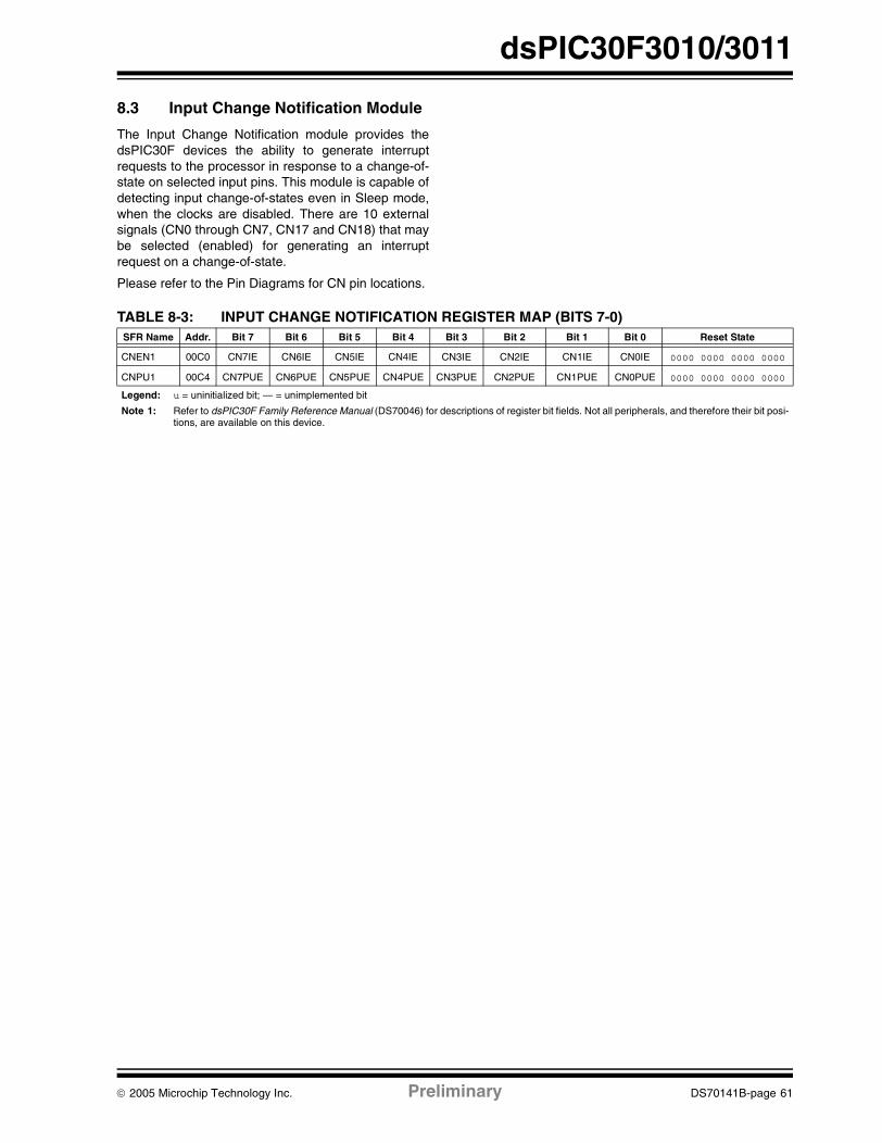
dsPIC30F3010/3011
8.3 Input Change Notification Module
The Input Change Notification module provides thedsPIC30F devices the ability to generate interruptrequests to the processor in response to a change-of-state on selected input pins. This module is capable ofdetecting input change-of-states even in Sleep mode,when the clocks are disabled. There are 10 externalsignals (CN0 through CN7, CN17 and CN18) that maybe selected (enabled) for generating an interruptrequest on a change-of-state.
Please refer to the Pin Diagrams for CN pin locations.
TABLE 8-3: INPUT CHANGE NOTIFICATION REGISTER MAP (BITS 7-0)SFR Name Addr. Bit 7 Bit 6 Bit 5 Bit 4 Bit 3 Bit 2 Bit 1 Bit 0 Reset State
CNEN1 00C0 CN7IE CN6IE CN5IE CN4IE CN3IE CN2IE CN1IE CN0IE 0000 0000 0000 0000
CNPU1 00C4 CN7PUE CN6PUE CN5PUE CN4PUE CN3PUE CN2PUE CN1PUE CN0PUE 0000 0000 0000 0000
Legend: u = uninitialized bit; — = unimplemented bit
Note 1: Refer to dsPIC30F Family Reference Manual (DS70046) for descriptions of register bit fields. Not all peripherals, and therefore their bit posi-tions, are available on this device.
© 2005 Microchip Technology Inc. Preliminary DS70141B-page 61

dsPIC30F3010/3011
NOTES:
DS70141B-page 62 Preliminary © 2005 Microchip Technology Inc.

dsPIC30F3010/3011
9.0 TIMER1 MODULE
This section describes the 16-bit General Purpose(GP) Timer1 module and associated operationalmodes. Figure 9-1 depicts the simplified block diagramof the 16-bit Timer1 Module.
The following sections provide a detailed description,including setup and control registers along with associ-ated block diagrams for the operational modes of thetimers.
The Timer1 module is a 16-bit timer which can serve asthe time counter for the real-time clock, or operate as afree running interval timer/counter. The 16-bit timer hasthe following modes:
• 16-bit Timer
• 16-bit Synchronous Counter• 16-bit Asynchronous Counter
Further, the following operational characteristics aresupported:
• Timer gate operation• Selectable prescaler settings• Timer operation during CPU Idle and Sleep
modes• Interrupt on 16-bit period register match or falling
edge of external gate signal
These operating modes are determined by setting theappropriate bit(s) in the 16-bit SFR, T1CON. Figure 9-1presents a block diagram of the 16-bit timer module.
16-bit Timer Mode: In the 16-bit Timer mode, the timerincrements on every instruction cycle up to a matchvalue, preloaded into the Period register PR1, thenresets to 0 and continues to count.
When the CPU goes into the Idle mode, the timer willstop incrementing, unless the TSIDL (T1CON<13>)bit = 0. If TSIDL = 1, the timer module logic will resumethe incrementing sequence upon termination of theCPU Idle mode.
16-bit Synchronous Counter Mode: In the 16-bitSynchronous Counter mode, the timer increments onthe rising edge of the applied external clock signal,which is synchronized with the internal phase clocks.The timer counts up to a match value preloaded in PR1,then resets to 0 and continues.
When the CPU goes into the Idle mode, the timer willstop incrementing, unless the respective TSIDL bit = 0.If TSIDL = 1, the timer module logic will resume theincrementing sequence upon termination of the CPUIdle mode.
16-bit Asynchronous Counter Mode: In the 16-bitAsynchronous Counter mode, the timer increments onevery rising edge of the applied external clock signal.The timer counts up to a match value preloaded in PR1,then resets to 0 and continues.
When the timer is configured for the Asynchronous modeof operation and the CPU goes into the Idle mode, thetimer will stop incrementing if TSIDL = 1.
Note: This data sheet summarizes features of this groupof dsPIC30F devices and is not intended to be a completereference source. For more information on the CPU,peripherals, register descriptions and general devicefunctionality, refer to the dsPIC30F Family ReferenceManual (DS70046).
Note: Timer1 is a ‘Type A’ timer. Please refer tothe specifications for a Type A timer inSection 23.0 "Electrical Characteris-tics" of this document.
© 2005 Microchip Technology Inc. Preliminary DS70141B-page 63

dsPIC30F3010/3011
FIGURE 9-1: 16-BIT TIMER1 MODULE BLOCK DIAGRAM (TYPE A TIMER)
9.1 Timer Gate Operation
The 16-bit timer can be placed in the Gated TimeAccumulation mode. This mode allows the internal TCY
to increment the respective timer when the gate inputsignal (T1CK pin) is asserted high. Control bit TGATE(T1CON<6>) must be set to enable this mode. Thetimer must be enabled (TON = 1) and the timer clocksource set to internal (TCS = 0).
When the CPU goes into the Idle mode, the timer willstop incrementing, unless TSIDL = 0. If TSIDL = 1, thetimer will resume the incrementing sequence upontermination of the CPU Idle mode.
9.2 Timer Prescaler
The input clock (FOSC/4 or external clock) to the 16-bitTimer, has a prescale option of 1:1, 1:8, 1:64 and 1:256selected by control bits TCKPS<1:0> (T1CON<5:4>).The prescaler counter is cleared when any of the fol-lowing occurs:
• a write to the TMR1 register• clearing of the TON bit (T1CON<15>)
• device Reset such as POR and BOR
However, if the timer is disabled (TON = 0), then thetimer prescaler cannot be reset since the prescalerclock is halted.
TMR1 is not cleared when T1CON is written. It iscleared by writing to the TMR1 register.
9.3 Timer Operation During Sleep Mode
During CPU Sleep mode, the timer will operate if:
• The timer module is enabled (TON = 1) and
• The timer clock source is selected as external (TCS = 1) and
• The TSYNC bit (T1CON<2>) is asserted to a logic 0, which defines the external clock source as asynchronous
When all three conditions are true, the timer willcontinue to count up to the Period register and be resetto 0x0000.
When a match between the timer and the Periodregister occurs, an interrupt can be generated, if therespective Timer Interrupt Enable bit is asserted.
TON
Sync
SOSCI
SOSCO/
PR1
T1IF
EqualComparator x 16
TMR1Reset
LPOSCEN
Event Flag
1
0
TSYNC
Q
Q D
CK
TGATE
TCKPS<1:0>
Prescaler 1, 8, 64, 256
2
TGATE
TCY
1
0
T1CK
TC
S
1 X
0 1
TG
AT
E
0 0
GateSync
DS70141B-page 64 Preliminary © 2005 Microchip Technology Inc.

dsPIC30F3010/3011
9.4 Timer Interrupt
The 16-bit timer has the ability to generate an interrupton period match. When the timer count matches thePeriod register, the T1IF bit is asserted and an interruptwill be generated, if enabled. The T1IF bit must becleared in software. The timer interrupt flag T1IF islocated in the IFS0 control register in the InterruptController.
When the Gated Time Accumulation mode is enabled,an interrupt will also be generated on the falling edge ofthe gate signal (at the end of the accumulation cycle).
Enabling an interrupt is accomplished via therespective Timer Interrupt Enable bit, T1IE. The TimerInterrupt Enable bit is located in the IEC0 controlregister in the Interrupt Controller.
9.5 Real-Time Clock
Timer1, when operating in Real-Time Clock (RTC)mode, provides time-of-day and event time stampingcapabilities. Key operational features of the RTC are:
• Operation from 32 kHz LP oscillator• 8-bit prescaler
• Low power • Real-Time Clock Interrupts
These Operating modes are determined by setting theappropriate bit(s) in the T1CON control register
FIGURE 9-2: RECOMMENDED COMPONENTS FOR TIMER1 LP OSCILLATOR RTC
9.5.1 RTC OSCILLATOR OPERATION
When the TON = 1, TCS = 1 and TGATE = 0, the timerincrements on the rising edge of the 32 kHz LP oscilla-tor output signal, up to the value specified in the Periodregister, and is then reset to ‘0’.
The TSYNC bit must be asserted to a logic ‘0’(Asynchronous mode) for correct operation.
Enabling LPOSCEN (OSCCON<1>) will disable thenormal Timer and Counter modes and enable a timercarry-out wake-up event.
When the CPU enters Sleep mode, the RTC willcontinue to operate, provided the 32 kHz externalcrystal oscillator is active and the control bits have notbeen changed. The TSIDL bit should be cleared to ‘0’in order for RTC to continue operation in Idle mode.
9.5.2 RTC INTERRUPTS
When an interrupt event occurs, the respectiveinterrupt flag, T1IF, is asserted and an interrupt will begenerated, if enabled. The T1IF bit must be cleared insoftware. The respective Timer interrupt flag, T1IF, islocated in the IFS0 status register in the InterruptController.
Enabling an interrupt is accomplished via therespective Timer Interrupt Enable bit, T1IE. The TimerInterrupt Enable bit is located in the IEC0 controlregister in the Interrupt Controller.
SOSCI
SOSCO
R
C1
C2
dsPIC30FXXXX32.768 kHzXTAL
C1 = C2 = 18 pF; R = 100K
© 2005 Microchip Technology Inc. Preliminary DS70141B-page 65
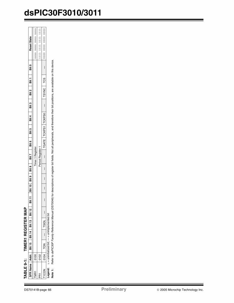
dsPIC30F3010/3011
TABL
E 9
-1:
TIM
ER
1 R
EG
IST
ER
MA
PS
FR
Nam
eA
dd
r.B
it 1
5B
it 1
4B
it 1
3B
it 1
2B
it 1
1B
it 1
0B
it 9
Bit
8B
it 7
Bit
6B
it 5
Bit
4B
it 3
Bit
2B
it 1
Bit
0R
eset
Sta
te
TM
R1
0100
Tim
er 1
Reg
iste
ruuuu uuuu uuuu uuuu
PR
101
02P
erio
d R
egis
ter
11111 1111 1111 1111
T1C
ON
0104
TO
N—
TS
IDL
——
——
——
TG
AT
ET
CK
PS
1T
CK
PS
0—
TS
YN
CT
CS
—0000 0000 0000 0000
Leg
end
:u
= u
nini
tializ
ed b
it; —
= u
nim
plem
ente
d bi
t
No
te1:
Ref
er to
dsP
IC30
F F
amily
Ref
eren
ce M
anua
l (D
S70
046)
for
desc
riptio
ns o
f reg
iste
r bi
t fie
lds.
Not
all
perip
hera
ls, a
nd th
eref
ore
thei
r bi
t pos
ition
s, a
re a
vaila
ble
on th
is d
evic
e.
DS70141B-page 66 Preliminary © 2005 Microchip Technology Inc.

dsPIC30F3010/3011
10.0 TIMER2/3 MODULE
This section describes the 32-bit General Purpose(GP) Timer module (Timer2/3) and associated opera-tional modes. Figure 10-1 depicts the simplified blockdiagram of the 32-bit Timer2/3 module. Figure 10-2and Figure 10-3 show Timer2/3 configured as twoindependent 16-bit timers; Timer2 and Timer3,respectively.
The Timer2/3 module is a 32-bit timer, which can beconfigured as two 16-bit timers, with selectable operat-ing modes. These timers are utilized by otherperipheral modules such as:
• Input Capture• Output Compare/Simple PWM
The following sections provide a detailed description,including setup and control registers, along withassociated block diagrams for the operational modes ofthe timers.
The 32-bit timer has the following modes:
• Two independent 16-bit timers (Timer2 and Timer3) with all 16-bit operating modes (except Asynchronous Counter mode)
• Single 32-bit Timer operation• Single 32-bit Synchronous Counter
Further, the following operational characteristics aresupported:
• ADC Event Trigger• Timer Gate Operation
• Selectable Prescaler Settings• Timer Operation during Idle and Sleep modes• Interrupt on a 32-bit Period Register Match
These operating modes are determined by setting theappropriate bit(s) in the 16-bit T2CON and T3CONSFRs.
For 32-bit timer/counter operation, Timer2 is the LSWord and Timer3 is the MS Word of the 32-bit timer.
16-bit Mode: In the 16-bit mode, Timer2 and Timer3can be configured as two independent 16-bit timers.Each timer can be set up in either 16-bit Timer mode or16-bit Synchronous Counter mode. See Section 9.0"Timer1 Module", Timer1 Module, for details on thesetwo operating modes.
The only functional difference between Timer2 andTimer3 is that Timer2 provides synchronization of theclock prescaler output. This is useful for high frequencyexternal clock inputs.
32-bit Timer Mode: In the 32-bit Timer mode, the timerincrements on every instruction cycle up to a matchvalue, preloads into the combined 32-bit period registerPR3/PR2, then resets to 0 and continues to count.
For synchronous 32-bit reads of the Timer2/Timer3pair, reading the LS word (TMR2 register) will causethe MS word to be read and latched into a 16-bitholding register, termed TMR3HLD.
For synchronous 32-bit writes, the holding register(TMR3HLD) must first be written to. When followed bya write to the TMR2 register, the contents of TMR3HLDwill be transferred and latched into the MSB of the32-bit timer (TMR3).
32-bit Synchronous Counter Mode: In the 32-bitSynchronous Counter mode, the timer increments onthe rising edge of the applied external clock signal,which is synchronized with the internal phase clocks.The timer counts up to a match value preloaded in thecombined 32-bit period register PR3/PR2, then resetsto ‘0’ and continues.
When the timer is configured for the SynchronousCounter mode of operation and the CPU goes into theIdle mode, the timer will stop incrementing, unless theTSIDL (T2CON<13>) bit = 0. If TSIDL = 1, the timermodule logic will resume the incrementing sequenceupon termination of the CPU Idle mode.
Note: This data sheet summarizes features of this groupof dsPIC30F devices and is not intended to be a completereference source. For more information on the CPU,peripherals, register descriptions and general devicefunctionality, refer to the dsPIC30F Family ReferenceManual (DS70046).
Note: Timer2 is a ‘Type B’ timer and Timer3 is a‘Type C’ timer. Please refer to theappropriate timer type in Section 23.0"Electrical Characteristics" of thisdocument.
Note: For 32-bit timer operation, T3CON controlbits are ignored. Only T2CON control bitsare used for setup and control. Timer 2clock and gate inputs are utilized for the32-bit timer module, but an interrupt isgenerated with the Timer3 interrupt flag(T3IF) and the interrupt is enabled with theTimer3 Interrupt Enable bit (T3IE).
© 2005 Microchip Technology Inc. Preliminary DS70141B-page 67

dsPIC30F3010/3011
FIGURE 10-1: 32-BIT TIMER2/3 BLOCK DIAGRAM
TMR3 TMR2
T3IF
Equal Comparator x 32
PR3 PR2
Reset
LSB MSB
Event Flag
Note: Timer Configuration bit T32, T2CON(<3>) must be set to 1 for a 32-bit timer/counter operation. All controlbits are respective to the T2CON register.
Data Bus<15:0>
TMR3HLD
Read TMR2
Write TMR216
16
16
Q
Q D
CK
TGATE(T2CON<6>)
(T2CON<6>)TGATE
0
1
TON
TCKPS<1:0>
Prescaler1, 8, 64, 256
2
TCY
TC
S
1 X
0 1
TG
AT
E
0 0
Gate
T2CK
Sync
ADC Event Trigger
Sync
DS70141B-page 68 Preliminary © 2005 Microchip Technology Inc.

dsPIC30F3010/3011
FIGURE 10-2: 16-BIT TIMER2 BLOCK DIAGRAM (TYPE B TIMER)
FIGURE 10-3: 16-BIT TIMER3 BLOCK DIAGRAM (TYPE C TIMER)
TON
Sync
PR2
T2IF
EqualComparator x 16
TMR2Reset
Event Flag
Q
Q D
CK
TGATE
TCKPS<1:0>
Prescaler1, 8, 64, 256
2
TGATE
TCY
1
0
TC
S
1 X
0 1
TG
AT
E
0 0
Gate
T2CK
Sync
TON
PR3
T3IF
EqualComparator x 16
TMR3Reset
Event Flag
Q
Q D
CK
TGATE
TCKPS<1:0>
Prescaler 1, 8, 64, 256
2
TGATE
TCY
1
0
TC
S
1 X
0 1
TG
AT
E
0 0
ADC Event Trigger
Sync
Note: The dsPIC30F3010/3011 devices do not have external pin inputs to TIMER3. In these devices the followingmodes should not be used:1. TCS = 12. TCS = 0 and TGATE = 1 (gated time accumulation)
© 2005 Microchip Technology Inc. Preliminary DS70141B-page 69

dsPIC30F3010/3011
10.1 Timer Gate Operation
The 32-bit timer can be placed in the Gated TimeAccumulation mode. This mode allows the internal TCY
to increment the respective timer when the gate inputsignal (T2CK pin) is asserted high. Control bit TGATE(T2CON<6>) must be set to enable this mode. When inthis mode, Timer2 is the originating clock source. TheTGATE setting is ignored for Timer3. The timer must beenabled (TON = 1) and the timer clock source set tointernal (TCS = 0).
The falling edge of the external signal terminates thecount operation, but does not reset the timer. The usermust reset the timer in order to start counting from zero.
10.2 ADC Event Trigger
When a match occurs between the 32-bit timer (TMR3/TMR2) and the 32-bit combined period register (PR3/PR2), a special ADC trigger event signal is generatedby Timer3.
10.3 Timer Prescaler
The input clock (FOSC/4 or external clock) to the timerhas a prescale option of 1:1, 1:8, 1:64, and 1:256selected by control bits TCKPS<1:0> (T2CON<5:4>and T3CON<5:4>). For the 32-bit timer operation, theoriginating clock source is Timer2. The prescaleroperation for Timer3 is not applicable in this mode. Theprescaler counter is cleared when any of the followingoccurs:
• a write to the TMR2/TMR3 register• clearing either of the TON (T2CON<15> or
T3CON<15>) bits to ‘0’• device Reset such as POR and BOR
However, if the timer is disabled (TON = 0), then theTimer 2 prescaler cannot be reset, since the prescalerclock is halted.
TMR2/TMR3 is not cleared when T2CON/T3CON iswritten.
10.4 Timer Operation During Sleep Mode
During CPU Sleep mode, the timer will not operate,because the internal clocks are disabled.
10.5 Timer Interrupt
The 32-bit timer module can generate an interrupt-on-period match, or on the falling edge of the external gatesignal. When the 32-bit timer count matches therespective 32-bit period register, or the falling edge ofthe external “gate” signal is detected, the T3IF bit(IFS0<7>) is asserted and an interrupt will be gener-ated if enabled. In this mode, the T3IF interrupt flag isused as the source of the interrupt. The T3IF bit mustbe cleared in software.
Enabling an interrupt is accomplished via therespective Timer Interrupt Enable bit, T3IE (IEC0<7>).
DS70141B-page 70 Preliminary © 2005 Microchip Technology Inc.

dsPIC30F3010/3011
TAB
LE
10-
1:TI
ME
R2/
3 R
EG
IST
ER
MA
PS
FR
Nam
eA
dd
r.B
it 1
5B
it 1
4B
it 1
3B
it 1
2B
it 1
1B
it 1
0B
it 9
Bit
8B
it 7
Bit
6B
it 5
Bit
4B
it 3
Bit
2B
it 1
Bit
0R
eset
Sta
te
TM
R2
0106
Tim
er2
Reg
iste
ruuuu uuuu uuuu uuuu
TM
R3H
LD01
08Ti
mer
3 H
oldi
ng R
egis
ter
(For
32-
bit t
imer
ope
ratio
ns o
nly)
uuuu uuuu uuuu uuuu
TM
R3
010A
Tim
er3
Reg
iste
ruuuu uuuu uuuu uuuu
PR
201
0CP
erio
d R
egis
ter
21111 1111 1111 1111
PR
301
0EP
erio
d R
egis
ter
31111 1111 1111 1111
T2C
ON
0110
TO
N—
TS
IDL
——
——
——
TG
AT
ET
CK
PS
1T
CK
PS
0T
32—
TC
S—
0000 0000 0000 0000
T3C
ON
0112
TO
N—
TS
IDL
——
——
——
TG
AT
ET
CK
PS
1T
CK
PS
0—
—T
CS
—0000 0000 0000 0000
Leg
end
:u
= u
nini
tializ
ed b
it; —
= u
nim
plem
ente
d bi
t
No
te1:
Ref
er to
dsP
IC30
F F
amily
Ref
eren
ce M
anua
l (D
S70
046)
for
desc
riptio
ns o
f reg
iste
r bi
t fie
lds.
Not
all
perip
hera
ls, a
nd th
eref
ore
thei
r bi
t pos
ition
s, a
re a
vaila
ble
on th
is d
evic
e.
© 2005 Microchip Technology Inc. Preliminary DS70141B-page 71

dsPIC30F3010/3011
NOTES:
DS70141B-page 72 Preliminary © 2005 Microchip Technology Inc.

dsPIC30F3010/3011
11.0 TIMER4/5 MODULE
This section describes the second 32-bit GeneralPurpose (GP) Timer module (Timer4/5) and associatedoperational modes. Figure 11-1 depicts the simplifiedblock diagram of the 32-bit Timer4/5 Module.Figure 11-2 and Figure 11-3 show Timer4/5 configuredas two independent 16-bit timers, Timer4 and Timer5,respectively.
The Timer4/5 module is similar in operation to theTimer 2/3 module. However, there are somedifferences, which are as follows:
• The Timer4/5 module does not support the ADC Event Trigger feature
• Timer4/5 can not be utilized by other peripheral modules such as Input Capture and Output Compare
The operating modes of the Timer4/5 module aredetermined by setting the appropriate bit(s) in the 16-bitT4CON and T5CON SFRs.
For 32-bit timer/counter operation, Timer4 is the LSWord and Timer5 is the MS Word of the 32-bit timer.
FIGURE 11-1: 32-BIT TIMER4/5 BLOCK DIAGRAM
Note: This data sheet summarizes features of this groupof dsPIC30F devices and is not intended to be a completereference source. For more information on the CPU,peripherals, register descriptions and general devicefunctionality, refer to the dsPIC30F Family ReferenceManual (DS70046).
Note: Timer4 is a ‘Type B’ timer and Timer5 is a‘Type C’ timer. Please refer to theappropriate timer type in Section 23.0"Electrical Characteristics" of thisdocument.
Note: For 32-bit timer operation, T5CON controlbits are ignored. Only T4CON control bitsare used for setup and control. Timer4clock and gate inputs are utilized for the32-bit timer module, but an interrupt isgenerated with the Timer5 interrupt flag(T5IF) and the interrupt is enabled with theTimer5 Interrupt Enable bit (T5IE).
TMR5 TMR4
T5IF
Equal Comparator x 32
PR5 PR4
Reset
LSB MSB
Event Flag
Note: Timer Configuration bit T32, T4CON(<3>) must be set to ‘1’ for a 32-bit timer/counter operation. Allcontrol bits are respective to the T4CON register.The dsPIC30F3010/3011 devices do not have external pin inputs to TIMER4 or TIMER5. In thesedevices the following modes should not be used:1. TCS = 12. TCS = 0 and TGATE = 1 (gated time accumulation)
Data Bus<15:0>
TMR5HLD
Read TMR4
Write TMR416
16
16
Q
Q D
CK
TGATE(T4CON<6>)
(T4CON<6>)TGATE
0
1
TON
TCKPS<1:0>
Prescaler 1, 8, 64, 256
2
TCY
TC
S
1 X
0 1
TG
AT
E
0 0
Gate
Sync
Sync
© 2005 Microchip Technology Inc. Preliminary DS70141B-page 73

dsPIC30F3010/3011
FIGURE 11-2: 16-BIT TIMER4 BLOCK DIAGRAM (TYPE B TIMER)
TON
Sync
PR4
T4IF
EqualComparator x 16
TMR4Reset
Event Flag
Q
Q D
CK
TGATE
TCKPS<1:0>
Prescaler 1, 8, 64, 256
2
TGATE
TCY
1
0
TC
S
1 X
0 1
TG
AT
E
0 0
GateSync
Note: The dsPIC30F3010/3011 devices do not have external pin inputs to TIMER4 or TIMER5. In thesedevices the following modes should not be used:1. TCS = 12. TCS = 0 and TGATE = 1 (gated time accumulation)
DS70141B-page 74 Preliminary © 2005 Microchip Technology Inc.

dsPIC30F3010/3011
FIGURE 11-3: 16-BIT TIMER5 BLOCK DIAGRAM (TYPE C TIMER)
TON
PR5
T5IF
EqualComparator x 16
TMR5Reset
Event Flag
Q
Q D
CK
TGATE
TCKPS<1:0>
Prescaler 1, 8, 64, 256
2
TGATE
TCY
1
0
TC
S
1 X
0 1
TG
AT
E
0 0
ADC Event Trigger
Sync
Note: The dsPIC30F3010/3011 devices do not have external pin inputs to TIMER4 or TIMER5. In thesedevices the following modes should not be used:1. TCS = 12. TCS = 0 and TGATE = 1 (gated time accumulation)
© 2005 Microchip Technology Inc. Preliminary DS70141B-page 75

dsPIC30F3010/3011
TABL
E 1
1-1:
TIM
ER
4/5
RE
GIS
TE
R M
AP
SF
R N
ame
Ad
dr.
Bit
15
Bit
14
Bit
13
Bit
12
Bit
11
Bit
10
Bit
9B
it 8
Bit
7B
it 6
Bit
5B
it 4
Bit
3B
it 2
Bit
1B
it 0
Res
et S
tate
TM
R4
0114
Tim
er 4
Reg
iste
ruuuu uuuu uuuu uuuu
TM
R5H
LD01
16T
imer
5 H
oldi
ng R
egis
ter
(For
32-
bit o
pera
tions
onl
y)uuuu uuuu uuuu uuuu
TM
R5
0118
Tim
er 5
Reg
iste
ruuuu uuuu uuuu uuuu
PR
401
1AP
erio
d R
egis
ter
41111 1111 1111 1111
PR
501
1CP
erio
d R
egis
ter
51111 1111 1111 1111
T4C
ON
011E
TO
N—
TS
IDL
——
——
——
TG
AT
ET
CK
PS
1T
CK
PS
0T
45—
TC
S—
0000 0000 0000 0000
T5C
ON
0120
TO
N—
TS
IDL
——
——
——
TG
AT
ET
CK
PS
1T
CK
PS
0—
—T
CS
—0000 0000 0000 0000
Leg
end
:u
= u
nini
tializ
ed b
it; —
= u
nim
plem
ente
d bi
t
No
te1:
Ref
er to
dsP
IC30
F F
amily
Ref
eren
ce M
anua
l (D
S70
046)
for
desc
riptio
ns o
f reg
iste
r bi
t fie
lds.
Not
all
perip
hera
ls, a
nd th
eref
ore
thei
r bi
t pos
ition
s, a
re a
vaila
ble
on th
is d
evic
e.
DS70141B-page 76 Preliminary © 2005 Microchip Technology Inc.

dsPIC30F3010/3011
12.0 INPUT CAPTURE MODULE
This section describes the Input Capture module andassociated operational modes. The features providedby this module are useful in applications requiringFrequency (Period) and Pulse measurement.Figure 12-1 depicts a block diagram of the InputCapture module. Input capture is useful for such modesas:
• Frequency/Period/Pulse Measurements• Additional sources of External Interrupts
The key operational features of the Input Capturemodule are:
• Simple Capture Event mode• Timer2 and Timer3 mode selection• Interrupt on input capture event
These operating modes are determined by settingthe appropriate bits in the ICxCON register(where x = 1,2,...,N).
FIGURE 12-1: INPUT CAPTURE MODE BLOCK DIAGRAM
Note: This data sheet summarizes features of this groupof dsPIC30F devices and is not intended to be a completereference source. For more information on the CPU,peripherals, register descriptions and general devicefunctionality, refer to the dsPIC30F Family ReferenceManual (DS70046).
Note: The dsPIC30F3010/3011 devices havefour capture channels. The channels aredesignated IC1, IC2, IC7 and IC8 tomaintain software compatibility with otherdsPIC30F devices
ICxBUF
Prescaler
ICx
ICM<2:0> Mode Select
3
Note: Where ‘x’ is shown, reference is made to the registers or bits associated to the respective inputcapture channels 1 through N.
1 0
Set Flag
Pin
ICxIF
ICTMR
T2_CNT T3_CNT
EdgeDetection
Logic
ClockSynchronizer1, 4, 16
From GP Timer Module
16 16
FIFOR/WLogic
ICI<1:0>
ICBNE, ICOV
ICxCONInterrupt
Logic
Set Flag ICxIF
Data Bus
© 2005 Microchip Technology Inc. Preliminary DS70141B-page 77

dsPIC30F3010/3011
12.1 Simple Capture Event Mode
The simple capture events in the dsPIC30F productfamily are:
• Capture every falling edge• Capture every rising edge
• Capture every 4th rising edge• Capture every 16th rising edge• Capture every rising and falling edge
These simple Input Capture modes are configured bysetting the appropriate bits ICM<2:0> (ICxCON<2:0>).
12.1.1 CAPTURE PRESCALER
There are four input capture prescaler settings, speci-fied by bits ICM<2:0> (ICxCON<2:0>). Whenever thecapture channel is turned off, the prescaler counter willbe cleared. In addition, any Reset will clear theprescaler counter.
12.1.2 CAPTURE BUFFER OPERATION
Each capture channel has an associated FIFO buffer,which is four 16-bit words deep. There are two statusflags, which provide status on the FIFO buffer:
• ICBFNE - Input Capture Buffer Not Empty• ICOV - Input Capture Overflow
The ICBFNE will be set on the first input capture eventand remain set until all capture events have been readfrom the FIFO. As each word is read from the FIFO, theremaining words are advanced by one position withinthe buffer.
In the event that the FIFO is full with four captureevents and a fifth capture event occurs prior to a readof the FIFO, an overflow condition will occur and theICOV bit will be set to a logic ‘1’. The fifth capture eventis lost and is not stored in the FIFO. No additionalevents will be captured till all four events have beenread from the buffer.
If a FIFO read is performed after the last read and nonew capture event has been received, the read willyield indeterminate results.
12.1.3 TIMER2 AND TIMER3 SELECTION MODE
Each capture channel can select between one of twotimers for the time base, Timer2 or Timer3.
Selection of the timer resource is accomplishedthrough SFR bit ICTMR (ICxCON<7>). Timer3 is thedefault timer resource available for the input capturemodule.
12.1.4 HALL SENSOR MODE
When the input capture module is set for capture onevery edge, rising and falling, ICM<2:0> = 001, thefollowing operations are performed by the inputcapture logic:
• The input capture interrupt flag is set on every edge, rising and falling.
• The interrupt on Capture Mode Setting bits, ICI<1:0>, is ignored, since every capture generates an interrupt.
• A capture overflow condition is not generated in this mode.
12.2 Input Capture Operation During Sleep and Idle Modes
An input capture event will generate a device wake-upor interrupt, if enabled, if the device is in CPU Idle orSleep mode.
Independent of the timer being enabled, the inputcapture module will wake-up from the CPU Sleep or Idlemode when a capture event occurs, if ICM<2:0> = 111and the Interrupt Enable bit is asserted. The samewake-up can generate an interrupt, if the conditions forprocessing the interrupt have been satisfied. The wake-up feature is useful as a method of adding extra externalpin interrupts.
12.2.1 INPUT CAPTURE IN CPU SLEEP MODE
CPU Sleep mode allows input capture module opera-tion with reduced functionality. In the CPU Sleepmode, the ICI<1:0> bits are not applicable, and theinput capture module can only function as an externalinterrupt source.
The capture module must be configured for interruptonly on the rising edge (ICM<2:0> = 111) in order forthe input capture module to be used while the deviceis in Sleep mode. The prescale settings of 4:1 or 16:1are not applicable in this mode.
DS70141B-page 78 Preliminary © 2005 Microchip Technology Inc.

dsPIC30F3010/3011
12.2.2 INPUT CAPTURE IN CPU IDLE MODE
CPU Idle mode allows input capture module operationwith full functionality. In the CPU Idle mode, the interruptmode selected by the ICI<1:0> bits are applicable, aswell as the 4:1 and 16:1 capture prescale settings,which are defined by control bits ICM<2:0>. This moderequires the selected timer to be enabled. Moreover, theICSIDL bit must be asserted to a logic ‘0’.
If the input capture module is defined as ICM<2:0> = 111in CPU Idle mode, the input capture pin will serve only asan external interrupt pin.
12.3 Input Capture Interrupts
The input capture channels have the ability to generatean interrupt, based upon the selected number ofcapture events. The selection number is set by controlbits ICI<1:0> (ICxCON<6:5>).
Each channel provides an interrupt flag (ICxIF) bit. Therespective capture channel interrupt flag is located inthe corresponding IFSx status register.
Enabling an interrupt is accomplished via the respec-tive capture channel interrupt enable (ICxIE) bit. TheCapture Interrupt Enable bit is located in thecorresponding IEC control register.
© 2005 Microchip Technology Inc. Preliminary DS70141B-page 79

dsPIC30F3010/3011
TABL
E 1
2-1:
INP
UT
CA
PT
UR
E R
EG
IST
ER
MA
PS
FR
Nam
eA
dd
r.B
it 1
5B
it 1
4B
it 1
3B
it 1
2B
it 1
1B
it 1
0B
it 9
Bit
8B
it 7
Bit
6B
it 5
Bit
4B
it 3
Bit
2B
it 1
Bit
0R
eset
Sta
te
IC1B
UF
0140
Inpu
t 1 C
aptu
re R
egis
ter
uuuu uuuu uuuu uuuu
IC1C
ON
0142
——
ICS
IDL
——
——
—IC
TM
RIC
I<1:
0>IC
OV
ICB
NE
ICM
<2:
0>0000 0000 0000 0000
IC2B
UF
0144
Inpu
t 2 C
aptu
re R
egis
ter
uuuu uuuu uuuu uuuu
IC2C
ON
0146
——
ICS
IDL
——
——
—IC
TM
RIC
I<1:
0>IC
OV
ICB
NE
ICM
<2:
0>0000 0000 0000 0000
IC7B
UF
0158
Inpu
t 7 C
aptu
re R
egis
ter
uuuu uuuu uuuu uuuu
IC7C
ON
015A
——
ICS
IDL
——
——
—IC
TM
RIC
I<1:
0>IC
OV
ICB
NE
ICM
<2:
0>0000 0000 0000 0000
IC8B
UF
015C
Inpu
t 8 C
aptu
re R
egis
ter
uuuu uuuu uuuu uuuu
IC8C
ON
015E
——
ICS
IDL
——
——
—IC
TM
RIC
I<1:
0>IC
OV
ICB
NE
ICM
<2:
0>0000 0000 0000 0000
Leg
end
:u
= u
nini
tializ
ed b
it; —
= u
nim
plem
ente
d bi
t
No
te1:
Ref
er to
dsP
IC30
F F
amily
Ref
eren
ce M
anua
l (D
S70
046)
for
desc
riptio
ns o
f reg
iste
r bi
t fie
lds.
Not
all
perip
hera
ls, a
nd th
eref
ore
thei
r bi
t pos
ition
s, a
re a
vaila
ble
on th
is d
evic
e.
DS70141B-page 80 Preliminary © 2005 Microchip Technology Inc.
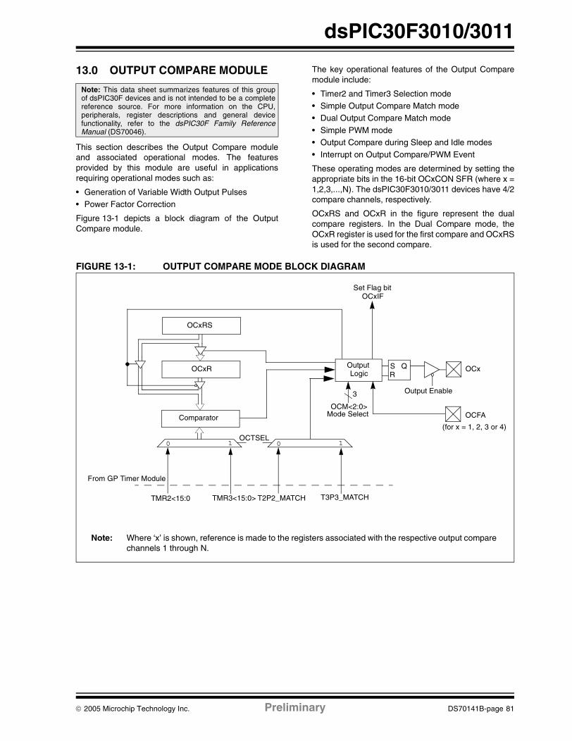
dsPIC30F3010/3011
13.0 OUTPUT COMPARE MODULE
This section describes the Output Compare moduleand associated operational modes. The featuresprovided by this module are useful in applicationsrequiring operational modes such as:
• Generation of Variable Width Output Pulses• Power Factor Correction
Figure 13-1 depicts a block diagram of the OutputCompare module.
The key operational features of the Output Comparemodule include:
• Timer2 and Timer3 Selection mode• Simple Output Compare Match mode• Dual Output Compare Match mode
• Simple PWM mode• Output Compare during Sleep and Idle modes• Interrupt on Output Compare/PWM Event
These operating modes are determined by setting theappropriate bits in the 16-bit OCxCON SFR (where x =1,2,3,...,N). The dsPIC30F3010/3011 devices have 4/2compare channels, respectively.
OCxRS and OCxR in the figure represent the dualcompare registers. In the Dual Compare mode, theOCxR register is used for the first compare and OCxRSis used for the second compare.
FIGURE 13-1: OUTPUT COMPARE MODE BLOCK DIAGRAM
Note: This data sheet summarizes features of this groupof dsPIC30F devices and is not intended to be a completereference source. For more information on the CPU,peripherals, register descriptions and general devicefunctionality, refer to the dsPIC30F Family ReferenceManual (DS70046).
OCxR
Comparator
OutputLogic
QSR
OCM<2:0>
Output Enable
OCx
Set Flag bitOCxIF
OCxRS
Mode Select
3
Note: Where ‘x’ is shown, reference is made to the registers associated with the respective output comparechannels 1 through N.
OCFA
OCTSEL0 1
T2P2_MATCHTMR2<15:0 TMR3<15:0> T3P3_MATCH
From GP Timer Module
(for x = 1, 2, 3 or 4)
0 1
© 2005 Microchip Technology Inc. Preliminary DS70141B-page 81

dsPIC30F3010/3011
13.1 Timer2 and Timer3 Selection Mode
Each output compare channel can select between oneof two 16-bit timers; Timer2 or Timer3.
The selection of the timers is controlled by the OCTSELbit (OCxCON<3>). Timer2 is the default timer resourcefor the Output Compare module.
13.2 Simple Output Compare Match Mode
When control bits OCM<2:0> (OCxCON<2:0>) = 001,010 or 011, the selected output compare channel isconfigured for one of three simple output comparematch modes:
• Compare forces I/O pin low• Compare forces I/O pin high• Compare toggles I/O pin
The OCxR register is used in these modes. The OCxRregister is loaded with a value and is compared to theselected incrementing timer count. When a compareoccurs, one of these compare match modes occurs. Ifthe counter resets to zero before reaching the value inOCxR, the state of the OCx pin remains unchanged.
13.3 Dual Output Compare Match Mode
When control bits OCM<2:0> (OCxCON<2:0>) = 100or 101, the selected output compare channel is config-ured for one of two dual output compare modes, whichare:
• Single Output Pulse mode• Continuous Output Pulse mode
13.3.1 SINGLE PULSE MODE
For the user to configure the module for the generationof a single output pulse, the following steps arerequired (assuming timer is off):
• Determine instruction cycle time TCY.
• Calculate desired pulse width value based on TCY.• Calculate time to start pulse from timer start value
of 0x0000.• Write pulse width start and stop times into OCxR
and OCxRS compare registers (x denotes channel 1, 2, ...,N).
• Set Timer Period register to value equal to, or greater than, value in OCxRS compare register.
• Set OCM<2:0> = 100.• Enable timer, TON (TxCON<15>) = 1.
To initiate another single pulse, issue another write toset OCM<2:0> = 100.
13.3.2 CONTINUOUS PULSE MODE
For the user to configure the module for the generationof a continuous stream of output pulses, the followingsteps are required:
• Determine instruction cycle time TCY.• Calculate desired pulse value based on TCY.• Calculate timer to start pulse width from timer start
value of 0x0000.• Write pulse width start and stop times into OCxR
and OCxRS (x denotes channel 1, 2, ...,N) compare registers, respectively.
• Set Timer Period register to value equal to, or greater than, value in OCxRS compare register.
• Set OCM<2:0> = 101.• Enable timer, TON (TxCON<15>) = 1.
13.4 Simple PWM Mode
When control bits OCM<2:0> (OCxCON<2:0>) = 110or 111, the selected output compare channel is config-ured for the PWM mode of operation. When configuredfor the PWM mode of operation, OCxR is the Main latch(read only) and OCxRS is the Secondary latch. Thisenables glitchless PWM transitions.
The user must perform the following steps in order toconfigure the output compare module for PWMoperation:
1. Set the PWM period by writing to the appropriateperiod register.
2. Set the PWM duty cycle by writing to the OCxRSregister.
3. Configure the output compare module for PWMoperation.
4. Set the TMRx prescale value and enable theTimer, TON (TxCON<15>) = 1.
13.4.1 INPUT PIN FAULT PROTECTION FOR PWM
When control bits OCM<2:0> (OCxCON<2:0>) = 111,the selected output compare channel is again config-ured for the PWM mode of operation, with the addi-tional feature of input fault protection. While in thismode, if a logic 0 is detected on the OCFA/B pin, therespective PWM output pin is placed in the high imped-ance input state. The OCFLT bit (OCxCON<4>) indi-cates whether a FAULT condition has occurred. Thisstate will be maintained until both of the followingevents have occurred:
• The external FAULT condition has been removed. • The PWM mode has been re-enabled by writing
to the appropriate control bits.
DS70141B-page 82 Preliminary © 2005 Microchip Technology Inc.

dsPIC30F3010/3011
13.4.2 PWM PERIOD
The PWM period is specified by writing to the PRxregister. The PWM period can be calculated usingEquation 13-1.
EQUATION 13-1: PWM PERIOD
PWM frequency is defined as 1 / [PWM period].
When the selected TMRx is equal to its respectiveperiod register, PRx, the following four events occur onthe next increment cycle:
• TMRx is cleared.
• The OCx pin is set.- Exception 1: If PWM duty cycle is 0x0000,
the OCx pin will remain low.- Exception 2: If duty cycle is greater than PRx,
the pin will remain high.• The PWM duty cycle is latched from OCxRS into
OCxR.• The corresponding timer interrupt flag is set.
See Figure 13-1 for key PWM period comparisons.Timer3 is referred to in the figure for clarity.
FIGURE 13-1: PWM OUTPUT TIMING
13.5 Output Compare Operation During CPU Sleep Mode
When the CPU enters the Sleep mode, all internalclocks are stopped. Therefore, when the CPU entersthe Sleep state, the output compare channel will drivethe pin to the active state that was observed prior toentering the CPU Sleep state.
For example, if the pin was high when the CPUentered the Sleep state, the pin will remain high. Like-wise, if the pin was low when the CPU entered theSleep state, the pin will remain low. In either case, theoutput compare module will resume operation whenthe device wakes up.
13.6 Output Compare Operation During CPU Idle Mode
When the CPU enters the Idle mode, the outputcompare module can operate with full functionality.
The output compare channel will operate during theCPU Idle mode if the OCSIDL bit (OCxCON<13>) is atlogic 0 and the selected time base (Timer2 or Timer3)is enabled and the TSIDL bit of the selected timer isset to logic 0.
13.7 Output Compare Interrupts
The output compare channels have the ability togenerate an interrupt on a compare match, forwhichever Match mode has been selected.
For all modes except the PWM mode, when a compareevent occurs, the respective interrupt flag (OCxIF) isasserted and an interrupt will be generated, if enabled.The OCxIF bit is located in the corresponding IFSstatus register, and must be cleared in software. Theinterrupt is enabled via the respective compareinterrupt enable (OCxIE) bit, located in thecorresponding IEC control register.
For the PWM mode, when an event occurs, the respec-tive timer interrupt flag (T2IF or T3IF) is asserted andan interrupt will be generated, if enabled. The IF bit islocated in the IFS0 status register, and must be clearedin software. The interrupt is enabled via the respectiveTimer Interrupt Enable bit (T2IE or T3IE), located in theIEC0 control register. The output compare interrupt flagis never set during the PWM mode of operation.
PWM period = [(PRx) + 1] • 4 • TOSC •(TMRx prescale value)
Period
Duty Cycle
TMR3 = Duty Cycle (OCxR) TMR3 = Duty Cycle (OCxR)
TMR3 = PR3
T3IF = 1(Interrupt Flag)
OCxR = OCxRS
TMR3 = PR3
(Interrupt Flag) OCxR = OCxRS
T3IF = 1
© 2005 Microchip Technology Inc. Preliminary DS70141B-page 83
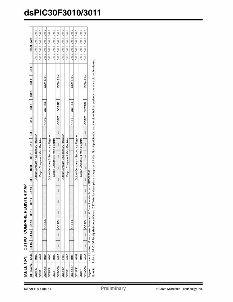
dsPIC30F3010/3011
TABL
E 1
3-1:
OU
TP
UT
CO
MP
AR
E R
EG
IST
ER
MA
PS
FR
Nam
eA
dd
r.B
it 1
5B
it 1
4B
it 1
3B
it 1
2B
it 1
1B
it 1
0B
it 9
Bit
8B
it 7
Bit
6B
it 5
Bit
4B
it 3
Bit
2B
it 1
Bit
0R
eset
Sta
te
OC
1RS
0180
Out
put C
ompa
re 1
Sec
onda
ry R
egis
ter
0000 0000 0000 0000
OC
1R01
82O
utpu
t Com
pare
1 M
ain
Reg
iste
r0000 0000 0000 0000
OC
1CO
N01
84—
—O
CS
IDL
——
——
——
——
OC
FLT
OC
TS
EL
OC
M<
2:0>
0000 0000 0000 0000
OC
2RS
0186
Out
put C
ompa
re 2
Sec
onda
ry R
egis
ter
0000 0000 0000 0000
OC
2R01
88O
utpu
t Com
pare
2 M
ain
Reg
iste
r0000 0000 0000 0000
OC
2CO
N01
8A—
—O
CS
IDL
——
——
——
——
OC
FLT
OC
TS
EO
CM
<2:
0>0000 0000 0000 0000
OC
3RS
*01
8CO
utpu
t Com
pare
3 S
econ
dary
Reg
iste
r0000 0000 0000 0000
OC
3R*
018E
Out
put C
ompa
re 3
Mai
n R
egis
ter
0000 0000 0000 0000
OC
3CO
N*
0190
——
OC
SID
L—
——
——
——
—O
CF
LTO
CT
SE
LO
CM
<2:
0>0000 0000 0000 0000
OC
4RS
*01
92O
utpu
t Com
pare
4 S
econ
dary
Reg
iste
r0000 0000 0000 0000
OC
4R*
0194
Out
put C
ompa
re 4
Mai
n R
egis
ter
0000 0000 0000 0000
OC
4CO
N*
0196
——
OC
SID
L—
——
——
——
—O
CF
LTO
CT
SE
LO
CM
<2:
0>0000 0000 0000 0000
Leg
end
:u
= u
nini
tializ
ed b
it; —
= u
nim
plem
ente
d bi
t, *
= n
ot a
vaila
ble
on d
sPIC
30F
3010
No
te1:
Ref
er to
dsP
IC30
F F
amily
Ref
eren
ce M
anua
l (D
S70
046)
for
desc
riptio
ns o
f reg
iste
r bi
t fie
lds.
Not
all
perip
hera
ls, a
nd th
eref
ore
thei
r bi
t pos
ition
s, a
re a
vaila
ble
on th
is d
evic
e.
DS70141B-page 84 Preliminary © 2005 Microchip Technology Inc.

dsPIC30F3010/3011
14.0 QUADRATURE ENCODER INTERFACE (QEI) MODULE
This section describes the Quadrature EncoderInterface (QEI) module and associated operationalmodes. The QEI module provides the interface toincremental encoders for obtaining mechanical positiondata.
The operational features of the QEI include:
• Three input channels for two phase signals and index pulse
• 16-bit up/down position counter• Count direction status
• Position Measurement (x2 and x4) mode• Programmable digital noise filters on inputs• Alternate 16-bit Timer/Counter mode
• Quadrature Encoder Interface interrupts
These operating modes are determined by setting theappropriate bits QEIM<2:0> (QEICON<10:8>).Figure 14-1 depicts the Quadrature Encoder Interfaceblock diagram.
FIGURE 14-1: QUADRATURE ENCODER INTERFACE BLOCK DIAGRAM
Note: This data sheet summarizes features of this groupof dsPIC30F devices and is not intended to be a completereference source. For more information on the CPU,peripherals, register descriptions and general devicefunctionality, refer to the dsPIC30F Family ReferenceManual (DS70046).
16-bit Up/Down Counter
Comparator/
Max Count Register
Quadrature
ProgrammableDigital Filter
QEA
ProgrammableDigital Filter
INDXUp/Down(1)
3
Encoder
ProgrammableDigital Filter
QEB
Interface Logic
QEIM<2:0> Mode Select
3
(POSCNT)
(MAXCNT)
QEIIFEvent Flag
Reset
Equal
2
TCY
1
0
TQCS TQCKPS<1:0>
2
1, 8, 64, 256 Prescaler
Q
QD
CKTQGATE
QEIM<2:0>
Synchronize
Det
1
0
Sleep Input
0
1
UPDN_SRC
QEICON<11>Zero Detect
Note 1: In dsPIC30F3010/3011, the UPDN pin is not available. Up/Down logic bit can still be polled by software.
© 2005 Microchip Technology Inc. Preliminary DS70141B-page 85

dsPIC30F3010/3011
14.1 Quadrature Encoder Interface Logic
A typical incremental (a.k.a. optical) encoder has threeoutputs: Phase A, Phase B and an index pulse. Thesesignals are useful and often required in position andspeed control of ACIM and SR motors.
The two channels, Phase A (QEA) and Phase B (QEB),have a unique relationship. If Phase A leads Phase B,then the direction (of the motor) is deemed positive orforward. If Phase A lags Phase B, then the direction (ofthe motor) is deemed negative or reverse.
A third channel, termed index pulse, occurs once perrevolution and is used as a reference to establish anabsolute position. The index pulse coincides withPhase A and Phase B, both low.
14.2 16-bit Up/Down Position Counter Mode
The 16-bit Up/Down Counter counts up or down onevery count pulse, which is generated by the differenceof the Phase A and Phase B input signals. The counteracts as an integrator, whose count value is proportionalto position. The direction of the count is determined bythe UPDN signal, which is generated by theQuadrature Encoder Interface Logic.
14.2.1 POSITION COUNTER ERROR CHECKING
Position count error checking in the QEI is provided forand indicated by the CNTERR bit (QEICON<15>). Theerror checking only applies when the position counteris configured for Reset on the Index Pulse modes(QEIM<2:0> = ‘110’ or ‘100’). In these modes, thecontents of the POSCNT register is compared with thevalues (0xFFFF or MAXCNT+1, depending on direc-tion). If these values are detected, an error condition isgenerated by setting the CNTERR bit and a QEI counterror interrupt is generated. The QEI count errorinterrupt can be disabled by setting the CEID bit(DFLTCON<8>). The position counter continues tocount encoder edges after an error has been detected.The POSCNT register continues to count up/down untila natural rollover/underflow. No interrupt is generatedfor the natural rollover/underflow event. The CNTERRbit is a Read/Write bit and reset in software by the user.
14.2.2 POSITION COUNTER RESET
The Position Counter Reset Enable bit, POSRES(QEI<2>) controls whether the position counter is resetwhen the index pulse is detected. This bit is onlyapplicable when QEIM<2:0> = ‘100’ or ‘110’.
If the POSRES bit is set to ‘1’, then the position counteris reset when the index pulse is detected. If thePOSRES bit is set to ‘0’, then the position counter is notreset when the index pulse is detected. The positioncounter will continue counting up or down, and will bereset on the rollover or underflow condition.
When selecting the INDX signal to reset the positioncounter (POSCNT), the user has to specify the stateson QEA and QEB input pins. These states have to bematched in order for a reset to occur. These states areselected by the IMV<1:0> bit in the DFLTCON <10:9>register.
The IMV<1:0> (Index Match Value) bit allows the userto specify the state of the QEA and QEB input pinsduring an index pulse when the POSCNT register is tobe reset.In 4X Quadrature Count Mode:IMV1 = Required State of Phase B input signal for
match on index pulseIMV0 = Required State of Phase A input signal for
match on index pulse
In 2X Quadrature Count Mode:IMV1 = Selects Phase input signal for index state
match (0 = Phase A, 1 = Phase B)IMV0 = Required State of the selected phase input
signal for match on index pulse
The interrupt is still generated on the detection of theindex pulse and not on the position counter overflow/underflow.
14.2.3 COUNT DIRECTION STATUS
As mentioned in the previous section, the QEI logicgenerates an UPDN signal, based upon the relation-ship between Phase A and Phase B. In addition to theoutput pin, the state of this internal UPDN signal issupplied to a SFR bit UPDN (QEICON<11>) as a readonly bit.
Note: QEI pins are multiplexed with analog inputs. User must insure that all QEI associated pins are set as digitalinputs in the ADPCFG register.
DS70141B-page 86 Preliminary © 2005 Microchip Technology Inc.
dsPIC30F3010/3011
14.3 Position Measurement Mode
There are two measurement modes which are sup-ported and are termed x2 and x4. These modes areselected by the QEIM<2:0> mode select bits located inSFR QEICON<10:8>.
When control bits QEIM<2:0> = 100 or 101, the x2Measurement mode is selected and the QEI logic onlylooks at the Phase A input for the position counterincrement rate. Every rising and falling edge of thePhase A signal causes the position counter to be incre-mented or decremented. The Phase B signal is stillutilized for the determination of the counter direction,just as in the x4 Measurement mode.
Within the x2 Measurement mode, there are twovariations of how the position counter is reset:
1. Position counter reset by detection of indexpulse, QEIM<2:0> = 100.
2. Position counter reset by match with MAXCNT,QEIM<2:0> = 101.
When control bits QEIM<2:0> = 110 or 111, the x4Measurement mode is selected and the QEI logic looksat both edges of the Phase A and Phase B inputsignals. Every edge of both signals causes the positioncounter to increment or decrement.
Within the x4 Measurement mode, there are twovariations of how the position counter is reset:
1. Position counter reset by detection of indexpulse, QEIM<2:0> = 110.
2. Position counter reset by match with MAXCNT,QEIM<2:0> = 111.
The x4 Measurement mode provides for finer resolu-tion data (more position counts) for determining motorposition.
14.4 Programmable Digital Noise Filters
The digital noise filter section is responsible for reject-ing noise on the incoming capture or quadraturesignals. Schmitt Trigger inputs and a three-clock cycledelay filter combine to reject low level noise and large,short duration noise spikes that typically occur in noiseprone applications, such as a motor system.
The filter ensures that the filtered output signal is notpermitted to change until a stable value has beenregistered for three consecutive clock cycles.
For the QEA, QEB and INDX pins, the clock dividefrequency for the digital filter is programmed by bitsQECK<2:0> (DFLTCON<6:4>) and are derived fromthe base instruction cycle TCY.
To enable the filter output for channels QEA, QEB andINDX, the QEOUT bit must be ‘1’. The filter network forall channels is disabled on POR and BOR.
14.5 Alternate 16-bit Timer/Counter
When the QEI module is not configured for the QEImode QEIM<2:0> = 001, the module can be configuredas a simple 16-bit timer/counter. The setup and controlof the auxiliary timer is accomplished through theQEICON SFR register. This timer functions identicallyto Timer1. The QEA pin is used as the timer clock input.
When configured as a timer, the POSCNT registerserves as the timer count register and the MAXCNTregister serves as the period register. When a timer/period register match occur, the QEI interrupt flag willbe asserted.
The only exception between the general purposetimers and this timer is the added feature of externalUp/Down input select. When the UPDN pin is assertedhigh, the timer will increment up. When the UPDN pinis asserted low, the timer will be decremented.
The UPDN Control/Status bit (QEICON<11>) can beused to select the count direction state of the timerregister. When UPDN = 1, the timer will count up. WhenUPDN = 0, the timer will count down.
In addition, control bit UPDN_SRC (QEICON<0>)determines whether the timer count direction state isbased on the logic state, written into the UPDN Control/Status bit (QEICON<11>), or the QEB pin state. WhenUPDN_SRC = 1, the timer count direction is controlledfrom the QEB pin. Likewise, when UPDN_SRC = 0, thetimer count direction is controlled by the UPDN bit.
14.6 QEI Module Operation During CPU Sleep Mode
14.6.1 QEI OPERATION DURING CPU SLEEP MODE
The QEI module will be halted during the CPU Sleepmode.
14.6.2 TIMER OPERATION DURING CPU SLEEP MODE
During CPU Sleep mode, the timer will not operate,because the internal clocks are disabled.
Note: Changing the operational mode (i.e., fromQEI to Timer or vice versa), will not affectthe timer/position count register contents.
Note: This Timer does not support the ExternalAsynchronous Counter mode of operation.If using an external clock source, the clockwill automatically be synchronized to theinternal instruction cycle.
© 2005 Microchip Technology Inc. Preliminary DS70141B-page 87

dsPIC30F3010/3011
14.7 QEI Module Operation During CPU Idle Mode
Since the QEI module can function as a quadratureencoder interface, or as a 16-bit timer, the followingsection describes operation of the module in bothmodes.
14.7.1 QEI OPERATION DURING CPU IDLE MODE
When the CPU is placed in the Idle mode, the QEImodule will operate if the QEISIDL bit(QEICON<13>) = 0. This bit defaults to a logic ‘0’upon executing POR and BOR. For halting the QEImodule during the CPU Idle mode, QEISIDL shouldbe set to ‘1’.
14.7.2 TIMER OPERATION DURING CPU IDLE MODE
When the CPU is placed in the Idle mode and the QEImodule is configured in the 16-bit Timer mode, the16-bit timer will operate if the QEISIDL bit(QEICON<13>) = 0. This bit defaults to a logic ‘0’ uponexecuting POR and BOR. For halting the timer moduleduring the CPU Idle mode, QEISIDL should be setto ‘1’.
If the QEISIDL bit is cleared, the timer will functionnormally, as if the CPU Idle mode had not beenentered.
14.8 Quadrature Encoder Interface Interrupts
The quadrature encoder interface has the ability togenerate an interrupt on occurrence of the followingevents:
• Interrupt on 16-bit up/down position counter rollover/underflow
• Detection of qualified index pulse, or if CNTERR bit is set
• Timer period match event (overflow/underflow)• Gate accumulation event
The QEI Interrupt Flag bit, QEIIF, is asserted uponoccurrence of any of the above events. The QEIIF bitmust be cleared in software. QEIIF is located in theIFS2 status register.
Enabling an interrupt is accomplished via the respec-tive Enable bit, QEIIE. The QEIIE bit is located in theIEC2 control register.
DS70141B-page 88 Preliminary © 2005 Microchip Technology Inc.

dsPIC30F3010/3011
TAB
LE
14-
1:Q
EI R
EG
IST
ER
MA
PS
FR
N
ame
Ad
dr.
Bit
15
Bit
14
Bit
13
Bit
12
Bit
11
Bit
10
Bit
9B
it 8
Bit
7B
it 6
Bit
5B
it 4
Bit
3B
it 2
Bit
1B
it 0
Res
et S
tate
QE
ICO
N01
22C
NT
ER
R—
QE
ISID
LIN
DX
UP
DN
QE
IM2
QE
IM1
QE
IM0
SW
PA
B—
TQ
GA
TE
TQ
CK
PS
1T
QC
KP
S0
PO
SR
ES
TQ
CS
UP
DN
_SR
C0000 0000 0000 0000
DF
LTC
ON
0124
——
——
—IM
V1
IMV
0C
EID
QE
OU
TQ
EC
K2
QE
CK
1Q
EC
K0
——
——
0000 0000 0000 0000
PO
SC
NT
0126
Pos
ition
Cou
nter
<15
:0>
0000 0000 0000 0000
MA
XC
NT
0128
Max
imun
Cou
nt<
15:0
>1111 1111 1111 1111
AD
PC
FG
02A
8—
——
——
——
PC
FG
8P
CF
G7
PC
FG
6P
CF
G5
PC
FG
4P
CF
G3
PC
FG
2P
CF
G1
PC
FG
00000 0000 0000 0000
Leg
end
:u
= u
nini
tializ
ed b
it; —
= u
nim
plem
ente
d bi
t
No
te1:
Ref
er to
dsP
IC30
F F
amily
Ref
eren
ce M
anua
l (D
S70
046)
for
desc
riptio
ns o
f reg
iste
r bi
t fie
lds.
Not
all
perip
hera
ls, a
nd th
eref
ore
thei
r bi
t pos
ition
s, a
re a
vaila
ble
on th
is d
evic
e.
© 2005 Microchip Technology Inc. Preliminary DS70141B-page 89
dsPIC30F3010/3011
NOTES:
DS70141B-page 90 Preliminary © 2005 Microchip Technology Inc.

dsPIC30F3010/3011
15.0 MOTOR CONTROL PWM MODULE
This module simplifies the task of generating multiple,synchronized Pulse Width Modulated (PWM) outputs.In particular, the following power and motion controlapplications are supported by the PWM module:
• Three Phase AC Induction Motor
• Switched Reluctance (SR) Motor• Brushless DC (BLDC) Motor• Uninterruptible Power Supply (UPS)
The PWM module has the following features:
• 6 PWM I/O pins with 3 duty cycle generators
• Up to 16-bit resolution
• ‘On-the-Fly’ PWM frequency changes• Edge and Center-aligned Output modes
• Single Pulse Generation mode• Interrupt support for asymmetrical updates in
Center-aligned mode• Output override control for Electrically
Commutative Motor (ECM) operation• ‘Special Event’ comparator for scheduling other
peripheral events • FAULT pins to optionally drive each of the PWM
output pins to a defined state
This module contains 3 duty cycle generators,numbered 1 through 3. The module has 6 PWM outputpins, numbered PWM1H/PWM1L through PWM3H/PWM3L. The six I/O pins are grouped into high/lownumbered pairs, denoted by the suffix H or L,respectively. For complementary loads, the low PWMpins are always the complement of the correspondinghigh I/O pin.
The PWM module allows several modes of operationwhich are beneficial for specific power controlapplications.
Note: This data sheet summarizes features of this groupof dsPIC30F devices and is not intended to be a completereference source. For more information on the CPU,peripherals, register descriptions and general devicefunctionality, refer to the dsPIC30F Family ReferenceManual (DS70046).
© 2005 Microchip Technology Inc. Preliminary DS70141B-page 91

dsPIC30F3010/3011
FIGURE 15-1: PWM MODULE BLOCK DIAGRAM
PDC3
PDC3 Buffer
PWMCON1
PTPER Buffer
PWMCON2
PTPER
PTMR
Comparator
Comparator
Channel 3 Dead-TimeGenerator and
PTCON
SEVTCMP
ComparatorSpecial Event Trigger
OVDCON
PWM Enable and Mode SFRs
PWM ManualControl SFR
Channel 2 Dead-TimeGenerator and
Channel 1 Dead-TimeGenerator and
PWM Generator#2
PWM Generator#1
PWM Generator #3
SEVTDIR
PTDIR
DTCON1 Dead-Time Control SFRs
Special EventPostscaler
PWM1L
PWM1H
PWM2L
PWM2H
Note: Details of PWM Generator #1 and #2 not shown for clarity.
16-b
it D
ata
Bus
PWM3L
PWM3H
FLTACON FAULT Pin Control SFRs
PWM time base
Output
Driver
Block
FLTA
Override Logic
Override Logic
Override Logic
DS70141B-page 92 Preliminary © 2005 Microchip Technology Inc.

dsPIC30F3010/3011
15.1 PWM Time Base
The PWM time base is provided by a 15-bit timer witha prescaler and postscaler. The time base is accessiblevia the PTMR SFR. PTMR<15> is a Read Only Statusbit, PTDIR, that indicates the present count direction ofthe PWM time base. If PTDIR is cleared, PTMR iscounting upwards. If PTDIR is set, PTMR is countingdownwards. The PWM time base is configured via thePTCON SFR. The time base is enabled/disabled bysetting/clearing the PTEN bit in the PTCON SFR.PTMR is not cleared when the PTEN bit is cleared insoftware.
The PTPER SFR sets the counting period for PTMR.The user must write a 15-bit value to PTPER<14:0>.When the value in PTMR<14:0> matches the value inPTPER<14:0>, the time base will either reset to 0, orreverse the count direction on the next occurring clockcycle. The action taken depends on the operatingmode of the time base.
The PWM time base can be configured for four differentmodes of operation:
• Free Running mode• Single Shot mode• Continuous Up/Down Count mode
• Continuous Up/Down Count mode with interrupts for double updates
These four modes are selected by the PTMOD<1:0>bits in the PTCON SFR. The Up/Down Counting modessupport center-aligned PWM generation. The SingleShot mode allows the PWM module to support pulsecontrol of certain Electronically Commutative Motors(ECMs).
The interrupt signals generated by the PWM time basedepend on the mode selection bits (PTMOD<1:0>) andthe postscaler bits (PTOPS<3:0>) in the PTCON SFR.
15.1.1 FREE RUNNING MODE
In the Free Running mode, the PWM time base countsupwards until the value in the Time Base Periodregister (PTPER) is matched. The PTMR register isreset on the following input clock edge and the timebase will continue to count upwards as long as thePTEN bit remains set.
When the PWM time base is in the Free Running mode(PTMOD<1:0> = 00), an interrupt event is generatedeach time a match with the PTPER register occurs andthe PTMR register is reset to zero. The postscalerselection bits may be used in this mode of the timer toreduce the frequency of the interrupt events.
15.1.2 SINGLE SHOT MODE
In the Single Shot Counting mode, the PWM time basebegins counting upwards when the PTEN bit is set.When the value in the PTMR register matches thePTPER register, the PTMR register will be reset on thefollowing input clock edge and the PTEN bit will becleared by the hardware to halt the time base.
When the PWM time base is in the Single Shot mode(PTMOD<1:0> = 01), an interrupt event is generatedwhen a match with the PTPER register occurs, thePTMR register is reset to zero on the following inputclock edge, and the PTEN bit is cleared. The postscalerselection bits have no effect in this mode of the timer.
15.1.3 CONTINUOUS UP/DOWN COUNTING MODES
In the Continuous Up/Down Counting modes, the PWMtime base counts upwards until the value in the PTPERregister is matched. The timer will begin countingdownwards on the following input clock edge. ThePTDIR bit in the PTCON SFR is read only and indicatesthe counting direction The PTDIR bit is set when thetimer counts downwards.
In the Up/Down Counting mode (PTMOD<1:0> = 10),an interrupt event is generated each time the value ofthe PTMR register becomes zero and the PWM timebase begins to count upwards. The postscaler selec-tion bits may be used in this mode of the timer to reducethe frequency of the interrupt events.
Note: If the period register is set to 0x0000, thetimer will stop counting, and the interruptand the special event trigger will not begenerated, even if the special event valueis also 0x0000. The module will not updatethe period register, if it is already at0x0000; therefore, the user must disablethe module in order to update the periodregister.
© 2005 Microchip Technology Inc. Preliminary DS70141B-page 93

dsPIC30F3010/3011
15.1.4 DOUBLE UPDATE MODE
In the Double Update mode (PTMOD<1:0> = 11), aninterrupt event is generated each time the PTMR regis-ter is equal to zero, as well as each time a period matchoccurs. The postscaler selection bits have no effect inthis mode of the timer.
The Double Update mode provides two additionalfunctions to the user. First, the control loop bandwidthis doubled because the PWM duty cycles can beupdated, twice per period. Second, asymmetricalcenter-aligned PWM waveforms can be generated,which are useful for minimizing output waveformdistortion in certain motor control applications.
15.1.5 PWM TIME BASE PRESCALER
The input clock to PTMR (FOSC/4), has prescaleroptions of 1:1, 1:4, 1:16, or 1:64, selected by controlbits PTCKPS<1:0> in the PTCON SFR. The prescalercounter is cleared when any of the following occurs:
• a write to the PTMR register• a write to the PTCON register• any device Reset
The PTMR register is not cleared when PTCON iswritten.
15.1.6 PWM TIME BASE POSTSCALER
The match output of PTMR can optionally be post-scaled through a 4-bit postscaler (which gives a 1:1 to1:16 scaling).
The postscaler counter is cleared when any of thefollowing occurs:
• a write to the PTMR register• a write to the PTCON register
• any device Reset
The PTMR register is not cleared when PTCON is written.
15.2 PWM Period
PTPER is a 15-bit register and is used to set the count-ing period for the PWM time base. PTPER is a doublebuffered register. The PTPER buffer contents areloaded into the PTPER register at the following instants:
• Free Running and Single Shot modes: When the PTMR register is reset to zero after a match with the PTPER register.
• Up/Down Counting modes: When the PTMR register is zero.
The value held in the PTPER buffer is automaticallyloaded into the PTPER register when the PWM timebase is disabled (PTEN = 0).
The PWM period can be determined usingEquation 15-1:
EQUATION 15-1: PWM PERIOD
If the PWM time base is configured for one of the Up/Down Count modes, the PWM period will be twice thevalue provided by Equation 15-1.
The maximum resolution (in bits) for a given deviceoscillator and PWM frequency can be determined usingEquation 15-2:
EQUATION 15-2: PWM RESOLUTION
15.3 Edge-Aligned PWM
Edge-aligned PWM signals are produced by the modulewhen the PWM time base is in the Free Running orSingle Shot mode. For edge-aligned PWM outputs, theoutput has a period specified by the value in PTPERand a duty cycle specified by the appropriate duty cycleregister (see Figure 15-2). The PWM output is drivenactive at the beginning of the period (PTMR = 0) and isdriven inactive when the value in the duty cycle registermatches PTMR.
If the value in a particular duty cycle register is zero,then the output on the corresponding PWM pin will beinactive for the entire PWM period. In addition, the out-put on the PWM pin will be active for the entire PWMperiod if the value in the duty cycle register is greaterthan the value held in the PTPER register.
FIGURE 15-2: EDGE-ALIGNED PWM
Note: Programming a value of 0x0001 in theperiod register could generate a continu-ous interrupt pulse, and hence, must beavoided.
TPWM =TCY • (PTPER + 1)
(PTMR Prescale Value)
Resolution =log (2 • TPWM / TCY)
log (2)
Period
Duty Cycle
0
PTPER
PTMRValue
New Duty Cycle Latched
DS70141B-page 94 Preliminary © 2005 Microchip Technology Inc.

dsPIC30F3010/3011
15.4 Center-Aligned PWM
Center-aligned PWM signals are produced by themodule when the PWM time base is configured in anUp/Down Counting mode (see Figure 15-3).
The PWM compare output is driven to the active statewhen the value of the duty cycle register matches thevalue of PTMR and the PWM time base is countingdownwards (PTDIR = 1). The PWM compare output isdriven to the inactive state when the PWM time base iscounting upwards (PTDIR = 0) and the value in thePTMR register matches the duty cycle value.
If the value in a particular duty cycle register is zero,then the output on the corresponding PWM pin will beinactive for the entire PWM period. In addition, the out-put on the PWM pin will be active for the entire PWMperiod if the value in the duty cycle register is equal tothe value held in the PTPER register.
FIGURE 15-3: CENTER-ALIGNED PWM
15.5 PWM Duty Cycle Comparison Units
There are three 16-bit special function registers (PDC1,PDC2 and PDC3) used to specify duty cycle values forthe PWM module.
The value in each duty cycle register determines theamount of time that the PWM output is in the activestate. The duty cycle registers are 16-bits wide. The LSbit of a duty cycle register determines whether thePWM edge occurs in the beginning. Thus, the PWMresolution is effectively doubled.
15.5.1 DUTY CYCLE REGISTER BUFFERS
The three PWM duty cycle registers are double buff-ered to allow glitchless updates of the PWM outputs.For each duty cycle, there is a duty cycle register thatis accessible by the user and a second duty cycleregister that holds the actual compare value used in thepresent PWM period.
For edge-aligned PWM output, a new duty cycle valuewill be updated whenever a match with the PTPERregister occurs and PTMR is reset. The contents of theduty cycle buffers are automatically loaded into theduty cycle registers when the PWM time base isdisabled (PTEN = 0) and the UDIS bit is cleared inPWMCON2.
When the PWM time base is in the Up/Down Countingmode, new duty cycle values are updated when thevalue of the PTMR register is zero and the PWM timebase begins to count upwards. The contents of the dutycycle buffers are automatically loaded into the dutycycle registers when the PWM time base is disabled(PTEN = 0).
When the PWM time base is in the Up/Down Countingmode with double updates, new duty cycle values areupdated when the value of the PTMR register is zero,and when the value of the PTMR register matches thevalue in the PTPER register. The contents of the dutycycle buffers are automatically loaded into the dutycycle registers when the PWM time base is disabled(PTEN = 0).
15.6 Complementary PWM Operation
In the Complementary mode of operation, each pair ofPWM outputs is obtained by a complementary PWMsignal. A dead-time may be optionally inserted duringdevice switching, when both outputs are inactive for ashort period (Refer to Section 15.7).
In Complementary mode, the duty cycle comparisonunits are assigned to the PWM outputs as follows:
• PDC1 register controls PWM1H/PWM1L outputs• PDC2 register controls PWM2H/PWM2L outputs• PDC3 register controls PWM3H/PWM3L outputs
The Complementary mode is selected for each PWMI/O pin pair by clearing the appropriate PMODx bit in thePWMCON1 SFR. The PWM I/O pins are set toComplementary mode by default upon a device Reset.
0
PTPERPTMRValue
Period
Period/2
DutyCycle
© 2005 Microchip Technology Inc. Preliminary DS70141B-page 95

dsPIC30F3010/3011
15.7 Dead-Time Generators
Dead-time generation may be provided when any ofthe PWM I/O pin pairs are operating in the Comple-mentary Output mode. The PWM outputs use Push-Pull drive circuits. Due to the inability of the power out-put devices to switch instantaneously, some amount oftime must be provided between the turn-off event ofone PWM output in a complementary pair and the turn-on event of the other transistor.
The PWM module allows two different dead-times to beprogrammed. These two dead-times may be used inone of two methods described below to increase userflexibility:
• The PWM output signals can be optimized fordifferent turn-off times in the high side and lowside transistors in a complementary pair oftransistors. The first dead-time is insertedbetween the turn-off event of the lower transistorof the complementary pair and the turn-on eventof the upper transistor. The second dead-time isinserted between the turn-off event of the uppertransistor and the turn-on event of the lowertransistor.
• The two dead-times can be assigned to individualPWM I/O pin pairs. This Operating mode allowsthe PWM module to drive different transistor/loadcombinations with each complementary PWM I/Opin pair.
15.7.1 DEAD-TIME GENERATORS
Each complementary output pair for the PWM modulehas a 6-bit down counter that is used to produce thedead-time insertion. As shown in Figure 15-4, eachdead-time unit has a rising and falling edge detectorconnected to the duty cycle comparison output.
15.7.2 DEAD-TIME RANGES
The amount of dead time provided by the dead-timeunit is selected by specifying the input clock prescalervalue and a 6-bit unsigned value.
Four input clock prescaler selections have been pro-vided to allow a suitable range of dead time, based onthe device operating frequency. The dead-time clockprescaler values are selected using the DTAPS<1:0>control bits in the DTCON1 SFR. One of four clockprescaler options (TCY, 2TCY, 4TCY or 8TCY) may beselected.
After the prescaler value is selected, the dead time isadjusted by loading 6-bit unsigned values into theDTCON1 SFR.
The dead time unit prescaler is cleared on the followingevents:
• On a load of the down timer due to a duty cycle comparison edge event.
• On a write to the DTCON1 register.
• On any device Reset.
FIGURE 15-4: DEAD-TIME TIMING DIAGRAM
Note: The user should not modify the DTCON1value while the PWM module is operating(PTEN = 1). Unexpected results mayoccur.
Duty Cycle Generator
PWMxH
PWMxL
Dead Time Dead Time
DS70141B-page 96 Preliminary © 2005 Microchip Technology Inc.
dsPIC30F3010/3011
15.8 Independent PWM Output
An independent PWM Output mode is required fordriving certain types of loads. A particular PWM outputpair is in the Independent Output mode when thecorresponding PMOD bit in the PWMCON1 register isset. No dead-time control is implemented betweenadjacent PWM I/O pins when the module is operatingin the Independent mode and both I/O pins are allowedto be active simultaneously.
In the Independent mode, each duty cycle generator isconnected to both of the PWM I/O pins in an outputpair. By using the associated duty cycle register andthe appropriate bits in the OVDCON register, the usermay select the following signal output options for eachPWM I/O pin operating in the Independent mode:
• I/O pin outputs PWM signal
• I/O pin inactive• I/O pin active
15.9 Single Pulse PWM Operation
The PWM module produces single pulse outputs whenthe PTCON control bits PTMOD<1:0> = 10. Only edge-aligned outputs may be produced in the Single Pulsemode. In Single Pulse mode, the PWM I/O pin(s) aredriven to the active state when the PTEN bit is set.When a match with a duty cycle register occurs, thePWM I/O pin is driven to the inactive state. When amatch with the PTPER register occurs, the PTMRregister is cleared, all active PWM I/O pins are drivento the inactive state, the PTEN bit is cleared and aninterrupt is generated.
15.10 PWM Output Override
The PWM output override bits allow the user tomanually drive the PWM I/O pins to specified logicstates, independent of the duty cycle comparison units.
All control bits associated with the PWM output over-ride function are contained in the OVDCON register.The upper half of the OVDCON register contains sixbits, POVDxH<3:1> and POVDxL<3:1>, that determinewhich PWM I/O pins will be overridden. The lower halfof the OVDCON register contains six bits,POUTxH<3:1> and POUTxL<3:1>, that determine thestate of the PWM I/O pins when a particular output isoverridden via the POVD bits.
15.10.1 COMPLEMENTARY OUTPUT MODE
When a PWMxL pin is driven active via the OVDCONregister, the output signal is forced to be the comple-ment of the corresponding PWMxH pin in the pair.Dead-time insertion is still performed when PWMchannels are overridden manually.
15.10.2 OVERRIDE SYNCHRONIZATION
If the OSYNC bit in the PWMCON2 register is set, alloutput overrides performed via the OVDCON registerare synchronized to the PWM time base. Synchronousoutput overrides occur at the following times:
• Edge-aligned mode, when PTMR is zero.• Center-aligned modes, when PTMR is zero and
when the value of PTMR matches PTPER.
© 2005 Microchip Technology Inc. Preliminary DS70141B-page 97

dsPIC30F3010/3011
15.11 PWM Output and Polarity Control
There are three device configuration bits associatedwith the PWM module that provide PWM output pincontrol:
• HPOL configuration bit• LPOL configuration bit• PWMPIN configuration bit
These three bits in the FPORBOR configuration regis-ter (see Section 21) work in conjunction with the threePWM Enable bits (PWMEN<3:1>) located in thePWMCON1 SFR. The configuration bits and PWMEnable bits ensure that the PWM pins are in the correctstates after a device Reset occurs. The PWMPIN con-figuration fuse allows the PWM module outputs to beoptionally enabled on a device Reset. If PWMPIN = 0,the PWM outputs will be driven to their inactive statesat Reset. If PWMPIN = 1 (default), the PWM outputswill be tri-stated. The HPOL bit specifies the polarity forthe PWMxH outputs, whereas the LPOL bit specifiesthe polarity for the PWMxL outputs.
15.11.1 OUTPUT PIN CONTROL
The PEN<3:1>H and PEN<3:1>L control bits in thePWMCON1 SFR enable each high PWM output pinand each low PWM output pin, respectively. If aparticular PWM output pin is not enabled, it is treatedas a general purpose I/O pin.
15.12 PWM FAULT Pin
There is one FAULT pin (FLTA) associated with thePWM module. When asserted, these pins can option-ally drive each of the PWM I/O pins to a defined state.
15.12.1 FAULT PIN ENABLE BITS
The FLTACON SFR has 3 control bits that determinewhether a particular pair of PWM I/O pins is to becontrolled by the FAULT input pin. To enable aspecific PWM I/O pin pair for FAULT overrides, thecorresponding bit should be set in the FLTACONregister.
If all enable bits are cleared in the FLTACON register,then the corresponding FAULT input pin has no effecton the PWM module and the pin may be used as ageneral purpose interrupt or I/O pin.
15.12.2 FAULT STATES
The FLTACON special function register has 6 bits thatdetermine the state of each PWM I/O pin when it isoverridden by a FAULT input. When these bits arecleared, the PWM I/O pin is driven to the inactive state.If the bit is set, the PWM I/O pin will be driven to theactive state. The active and inactive states are refer-enced to the polarity defined for each PWM I/O pin(HPOL and LPOL polarity control bits).
A special case exists when a PWM module I/O pair isin the Complementary mode and both pins are pro-grammed to be active on a FAULT condition. ThePWMxH pin always has priority in the Complementarymode, so that both I/O pins cannot be driven activesimultaneously.
15.12.3 FAULT INPUT MODES
The FAULT input pin has two modes of operation:
• Latched Mode: When the FAULT pin is driven low, the PWM outputs will go to the states defined in the FLTACON register. The PWM outputs will remain in this state until the FAULT pin is driven high and the corresponding interrupt flag has been cleared in software. When both of these actions have occurred, the PWM outputs will return to normal operation at the beginning of the next PWM cycle or half-cycle boundary. If the interrupt flag is cleared before the FAULT condi-tion ends, the PWM module will wait until the FAULT pin is no longer asserted, to restore the outputs.
• Cycle-by-Cycle Mode: When the FAULT input pin is driven low, the PWM outputs remain in the defined FAULT states for as long as the FAULT pin is held low. After the FAULT pin is driven high, the PWM outputs return to normal operation at the beginning of the following PWM cycle or half-cycle boundary.
The Operating mode for the FAULT input pin isselected using the FLTAM control bit in the FLTACONspecial function register.
The FAULT pin can be controlled manually in software.
Note: The FAULT pin logic can operate indepen-dent of the PWM logic. If all the enable bitsin the FLTACON register are cleared, thenthe FAULT pin could be used as a generalpurpose interrupt pin. The FAULT pin hasan interrupt vector, Interrupt Flag bit andInterrupt Priority bits associated with it.
DS70141B-page 98 Preliminary © 2005 Microchip Technology Inc.
dsPIC30F3010/3011
15.13 PWM Update Lockout
For a complex PWM application, the user may need towrite up to three duty cycle registers and the Time BasePeriod register, PTPER, at a given time. In some appli-cations, it is important that all buffer registers be writtenbefore the new duty cycle and period values are loadedfor use by the module.
The PWM update lockout feature is enabled by settingthe UDIS control bit in the PWMCON2 SFR. The UDISbit affects all duty cycle buffer registers and the PWMTime Base Period buffer, PTPER. No duty cyclechanges or period value changes will have effect whileUDIS = 1.
15.14 PWM Special Event Trigger
The PWM module has a special event trigger thatallows A/D conversions to be synchronized to the PWMtime base. The A/D sampling and conversion time maybe programmed to occur at any point within the PWMperiod. The special event trigger allows the user to min-imize the delay between the time when A/D conversionresults are acquired and the time when the duty cyclevalue is updated.
The PWM special event trigger has a SFR namedSEVTCMP, and five control bits to control its operation.The PTMR value for which a special event triggershould occur is loaded into the SEVTCMP register.When the PWM time base is in an Up/Down Countingmode, an additional control bit is required to specify thecounting phase for the special event trigger. The countphase is selected using the SEVTDIR control bit in theSEVTCMP SFR. If the SEVTDIR bit is cleared, thespecial event trigger will occur on the upward countingcycle of the PWM time base. If the SEVTDIR bit is set,the special event trigger will occur on the downwardcount cycle of the PWM time base. The SEVTDIRcontrol bit has no effect unless the PWM time base isconfigured for an Up/Down Counting mode.
15.14.1 SPECIAL EVENT TRIGGER POSTSCALER
The PWM special event trigger has a postscaler thatallows a 1:1 to 1:16 postscale ratio. The postscaler isconfigured by writing the SEVOPS<3:0> control bits inthe PWMCON2 SFR.
The special event output postscaler is cleared on thefollowing events:
• Any write to the SEVTCMP register• Any device Reset
15.15 PWM Operation During CPU Sleep Mode
The FAULT A input pin has the ability to wake the CPUfrom Sleep mode. The PWM module generates aninterrupt if the FAULT pin is driven low while in Sleep.
15.16 PWM Operation During CPU Idle Mode
The PTCON SFR contains a PTSIDL control bit. Thisbit determines if the PWM module will continue tooperate or stop when the device enters Idle mode. IfPTSIDL = 0, the module will continue to operate. IfPTSIDL = 1, the module will stop operation as long asthe CPU remains in Idle mode.
© 2005 Microchip Technology Inc. Preliminary DS70141B-page 99

dsPIC30F3010/3011
TABL
E 1
5-1:
PW
M R
EG
IST
ER
MA
P
SF
R N
ame
Ad
dr.
Bit
15
Bit
14
Bit
13
Bit
12
Bit
11
Bit
10
Bit
9B
it 8
Bit
7B
it 6
Bit
5B
it 4
Bit
3B
it 2
Bit
1B
it 0
Res
et S
tate
PT
CO
N01
C0
PT
EN
—P
TS
IDL
——
——
—P
TO
PS
<3:
0>P
TC
KP
S<
1:0>
PT
MO
D<
1:0>
0000 0000 0000 0000
PT
MR
01C
2P
TD
IRP
WM
Tim
er C
ount
Val
ue0000 0000 0000 0000
PT
PE
R01
C4
—P
WM
Tim
e B
ase
Per
iod
Reg
iste
r0000 0000 0000 0000
SE
VT
CM
P01
C6
SE
VT
DIR
PW
M S
peci
al E
vent
Com
pare
Reg
iste
r0000 0000 0000 0000
PW
MC
ON
101
C8
——
——
—P
TM
OD
3P
TM
OD
2P
TM
OD
1—
PE
N3H
PE
N2H
PE
N1H
—P
EN
3LP
EN
2LP
EN
1L0000 0000 1111 1111
PW
MC
ON
201
CA
——
——
SE
VO
PS
<3:
0>—
——
——
—O
SY
NC
UD
IS0000 0000 0000 0000
DT
CO
N1
01C
C—
——
——
——
—D
TAP
S<
1:0>
Dea
d-T
ime
A V
alue
0000 0000 0000 0000
FLT
AC
ON
01D
0—
—FA
OV
3HFA
OV
3LFA
OV
2HFA
OV
2LFA
OV
1HFA
OV
1LF
LTA
M—
——
—FA
EN
3FA
EN
2FA
EN
10000 0000 0000 0000
OV
DC
ON
01D
4—
—P
OV
D3H
PO
VD
3LP
OV
D2H
PO
VD
2LP
OV
D1H
PO
VD
1L—
—P
OU
T3H
PO
UT
3LP
OU
T2H
PO
UT
2LP
OU
T1H
PO
UT
1L1111 1111 0000 0000
PD
C1
01D
6P
WM
Dut
y C
ycle
#1
Reg
iste
r0000 0000 0000 0000
PD
C2
01D
8P
WM
Dut
y C
ycle
#2
Reg
iste
r0000 0000 0000 0000
PD
C3
01D
AP
WM
Dut
y C
ycle
#3
Reg
iste
r0000 0000 0000 0000
Leg
end
:u
= u
nini
tializ
ed b
it; —
= u
nim
plem
ente
d bi
t
No
te1:
Ref
er to
dsP
IC30
F F
amily
Ref
eren
ce M
anua
l (D
S70
046)
for
desc
riptio
ns o
f reg
iste
r bi
t fie
lds.
Not
all
perip
hera
ls, a
nd th
eref
ore
thei
r bi
t pos
ition
s, a
re a
vaila
ble
on th
is d
evic
e.
DS70141B-page 100 Preliminary © 2005 Microchip Technology Inc.

dsPIC30F3010/3011
16.0 SPI™ MODULE
The Serial Peripheral Interface (SPI) module is asynchronous serial interface. It is useful forcommunicating with other peripheral devices such asEEPROMs, shift registers, display drivers and A/Dconverters, or other microcontrollers. It is compatiblewith SPI and SIOP interfaces available on some othermicrocontrollers.
16.1 Operating Function Description
The SPI module consists of a 16-bit Shift register,SPI1SR, used for shifting data in and out, and a Bufferregister, SPI1BUF. A Control register, SPI1CON,configures the module. Additionally, a Status register,SPI1STAT, indicates various status conditions.
The serial interface consists of 4 pins: SDI1 (serialdata input), SDO1 (serial data output), SCK1 (shiftclock input or output), and SS1 (active low slaveselect).
In Master mode operation, SCK is a clock output, butin Slave mode, it is a clock input.
A series of eight (8) or sixteen (16) clock pulses shiftsout bits from the SPI1SR to SDO1 pin andsimultaneously shifts in data from SDI1 pin. Aninterrupt is generated when the transfer is completeand the corresponding Interrupt Flag bit (SPI1IF) isset. This interrupt can be disabled through an InterruptEnable bit (SPI1IE).
The receive operation is double buffered. When acomplete byte is received, it is transferred fromSPI1SR to SPI1BUF.
If the receive buffer is full when new data is beingtransferred from SPI1SR to SPI1BUF, the module willset the SPIROV bit, indicating an overflow condition.The transfer of the data from SPI1SR to SPI1BUF willnot be completed and the new data will be lost. Themodule will not respond to SCL transitions whileSPIROV is 1, effectively disabling the module untilSPI1BUF is read by user software.
Transmit writes are also double buffered. The userwrites to SPI1BUF. When the master or slave transferis completed, the contents of the Shift register(SPI1SR) are moved to the receive buffer. If any trans-mit data has been written to the Buffer register, thecontents of the transmit buffer are moved to SPI1SR.The received data is thus placed in SPI1BUF and thetransmit data in SPI1SR is ready for the next transfer.
In Master mode, the clock is generated by prescalingthe system clock. Data is transmitted as soon as avalue is written to SPI1BUF. The interrupt is generatedat the middle of the transfer of the last bit.
In Slave mode, data is transmitted and received asexternal clock pulses appear on SCK. Again, theinterrupt is generated when the last bit is latched. IfSSx control is enabled, then transmission andreception are enabled only when SSx = low. TheSDOx output will be disabled in SSx mode with SSxhigh.
The clock provided to the module is (FOSC/4). Thisclock is then prescaled by the primary (PPRE<1:0>)and the secondary (SPRE<2:0>) prescale factors. TheCKE bit determines whether transmit occurs on transi-tion from active clock state to Idle clock state, or viceversa. The CKP bit selects the Idle state (high or low)for the clock.
16.1.1 WORD AND BYTE COMMUNICATION
A control bit, MODE16 (SPI1CON<10>), allows themodule to communicate in either 16-bit or 8-bit mode.16-bit operation is identical to 8-bit operation, exceptthat the number of bits transmitted is 16 instead of 8.
The user software must disable the module prior tochanging the MODE16 bit. The SPI module is resetwhen the MODE16 bit is changed by the user.
A basic difference between 8-bit and 16-bit operation isthat the data is transmitted out of bit 7 of the SPIxSR for8-bit operation, and data is transmitted out of bit 15 ofthe SPIxSR for 16-bit operation. In both modes, data isshifted into bit 0 of the SPIxSR.
16.1.2 SDO1 DISABLE
A control bit, DISSDO, is provided to the SPI1CONregister to allow the SDO1 output to be disabled. Thiswill allow the SPI module to be connected in an inputonly configuration. SDO can also be used for generalpurpose I/O.
16.2 Framed SPI Support
The module supports a basic framed SPI protocol inMaster or Slave mode. The control bit FRMEN enablesframed SPI support and causes the SS1 pin to performthe frame synchronization pulse (FSYNC) function.The control bit SPIFSD determines whether the SS1pin is an input or an output (i.e., whether the modulereceives or generates the frame synchronizationpulse). The frame pulse is an active high pulse for asingle SPI clock cycle. When frame synchronization isenabled, the data transmission starts only on thesubsequent transmit edge of the SPI clock.
Note: This data sheet summarizes features of this groupof dsPIC30F devices and is not intended to be a completereference source. For more information on the CPU,peripherals, register descriptions and general devicefunctionality, refer to the dsPIC30F Family ReferenceManual (DS70046).
Note: Both the transmit buffer (SPI1TXB) andthe receive buffer (SPI1RXB) are mappedto the same register address, SPI1BUF.
© 2005 Microchip Technology Inc. Preliminary DS70141B-page 101

dsPIC30F3010/3011
FIGURE 16-1: SPI™ BLOCK DIAGRAM
FIGURE 16-2: SPI™ MASTER/SLAVE CONNECTION
Note: In dsPIC30F4012, the SS1 pin is not available.
Read Write
InternalData Bus
SDI1
SDO1
SS1
SCK1
SPI1SR
SPI1BUF
bit0
Shiftclock
EdgeSelect
FCYPrimary
1, 4, 16, 64
Enable Master Clock
PrescalerSecondaryPrescaler1:1 – 1:8
SS & FSYNC
Control
ClockControl
Transmit
SPI1BUF
Receive
Serial Input Buffer(SPIxBUF)
Shift Register(SPIxSR)
MSb LSb
SDOx
SDIx
PROCESSOR 1
SCKx
SPI™ Master
Serial Input Buffer(SPIyBUF)
Shift Register(SPIySR)
LSbMSb
SDIy
SDOy
PROCESSOR 2
SCKy
SPI™ Slave
Serial Clock
Note: x = 1 or 2, y = 1 or 2.
DS70141B-page 102 Preliminary © 2005 Microchip Technology Inc.

dsPIC30F3010/3011
16.3 Slave Select Synchronization
The SS1 pin allows a Synchronous Slave mode. TheSPI must be configured in SPI Slave mode, with SS1pin control enabled (SSEN = 1). When the SS1 pin islow, transmission and reception are enabled and theSDO1 pin is driven. When SS1 pin goes high, theSDO1 pin is no longer driven. Also, the SPI module isre-synchronized and all counters/control circuitry arereset. Therefore, when the SS1 pin is asserted lowagain, transmission/reception will begin at the MS bit,even if SS1 has been de-asserted in the middle of atransmit/receive. Note that in dsPIC30F4012, the SS1pin is not available.
16.4 SPI Operation During CPU Sleep Mode
During Sleep mode, the SPI module is shut-down. Ifthe CPU enters Sleep mode while an SPI transactionis in progress, then the transmission and reception isaborted.
The transmitter and receiver will stop in Sleep mode.However, register contents are not affected byentering or exiting Sleep mode.
16.5 SPI Operation During CPU Idle Mode
When the device enters Idle mode, all clock sourcesremain functional. The SPISIDL bit (SPI1STAT<13>)selects if the SPI module will stop or continue on Idle.If SPISIDL = 0, the module will continue to operatewhen the CPU enters Idle mode. If SPISIDL = 1, themodule will stop when the CPU enters Idle mode.
© 2005 Microchip Technology Inc. Preliminary DS70141B-page 103

dsPIC30F3010/3011
TABL
E 1
6-1:
SP
I1 R
EG
IST
ER
MA
PS
FR
N
ame
Ad
dr.
Bit
15
Bit
14
Bit
13
Bit
12
Bit
11
Bit
10
Bit
9B
it 8
Bit
7B
it 6
Bit
5B
it 4
Bit
3B
it 2
Bit
1B
it 0
Res
et S
tate
SP
I1S
TAT
0220
SP
IEN
—S
PIS
IDL
——
——
——
SP
IRO
V—
——
—S
PIT
BF
SP
IRB
F0000 0000 0000 0000
SP
I1C
ON
0222
—F
RM
EN
SP
IFS
D—
DIS
SD
OM
OD
E16
SM
PC
KE
SS
EN
CK
PM
ST
EN
SP
RE
2S
PR
E1
SP
RE
0P
PR
E1
PP
RE
00000 0000 0000 0000
SP
I1B
UF
0224
Tran
smit
and
Rec
eive
Buf
fer
0000 0000 0000 0000
Leg
end
:u
= u
nini
tializ
ed b
it; —
= u
nim
plem
ente
d bi
t
No
te1:
Ref
er to
dsP
IC30
F F
amily
Ref
eren
ce M
anua
l (D
S70
046)
for
desc
riptio
ns o
f reg
iste
r bi
t fie
lds.
Not
all
perip
hera
ls, a
nd th
eref
ore
thei
r bi
t pos
ition
s, a
re a
vaila
ble
on th
is d
evic
e.
DS70141B-page 104 Preliminary © 2005 Microchip Technology Inc.

dsPIC30F3010/3011
17.0 I2C MODULE
The Inter-Integrated Circuit (I2CTM) module providescomplete hardware support for both Slave and Multi-Master modes of the I2C serial communicationstandard, with a 16-bit interface.
This module offers the following key features:
• I2C interface supporting both master and slave operation.
• I2C Slave mode supports 7 and 10-bit address.• I2C Master mode supports 7 and 10-bit address.• I2C port allows bidirectional transfers between
master and slaves.• Serial clock synchronization for I2C port can be
used as a handshake mechanism to suspend and resume serial transfer (SCLREL control).
• I2C supports multi-master operation; detects bus collision and will arbitrate accordingly.
17.1 Operating Function Description
The hardware fully implements all the master andslave functions of the I2C Standard and Fast modespecifications, as well as 7 and 10-bit addressing.
Thus, the I2C module can operate either as a slave ora master on an I2C bus.
17.1.1 VARIOUS I2C MODES
The following types of I2C operation are supported:
• I2C Slave operation with 7-bit address
• I2C Slave operation with 10-bit address• I2C Master operation with 7- or 10-bit address
See the I2C programmer’s model in Figure 17-1.
17.1.2 PIN CONFIGURATION IN I2C MODE
I2C has a 2-pin interface; pin SCL is clock and pin SDAis data.
17.1.3 I2C REGISTERS
I2CCON and I2CSTAT are Control and Statusregisters, respectively. The I2CCON register is read-able and writable. The lower 6 bits of I2CSTAT are readonly. The remaining bits of the I2CSTAT are read/write.
I2CRSR is the Shift register used for shifting data,whereas I2CRCV is the Buffer register to which databytes are written, or from which data bytes are read.I2CRCV is the receive buffer, as shown in Figure 17-1.I2CTRN is the Transmit register to which bytes arewritten during a transmit operation, as shown inFigure 17-2.
The I2CADD register holds the slave address. A statusbit, ADD10, indicates 10-bit Address mode. TheI2CBRG acts as the Baud Rate Generator (BRG)reload value.
In receive operations, I2CRSR and I2CRCV togetherform a double buffered receiver. When I2CRSRreceives a complete byte, it is transferred to I2CRCVand an interrupt pulse is generated. Duringtransmission, the I2CTRN is not double buffered.
FIGURE 17-1: PROGRAMMER’S MODEL
Note: This data sheet summarizes features of this groupof dsPIC30F devices and is not intended to be a completereference source. For more information on the CPU,peripherals, register descriptions and general devicefunctionality, refer to the dsPIC30F Family ReferenceManual (DS70046).
Note: Following a Restart condition in 10-bitmode, the user only needs to match thefirst 7-bit address.
bit 7 bit 0I2CRCV (8 bits)
bit 7 bit 0I2CTRN (8 bits)
bit 8 bit 0I2CBRG (9 bits)
bit 15 bit 0I2CCON (16-bits)
bit 15 bit 0I2CSTAT (16-bits)
bit 9 bit 0I2CADD (10-bits)
© 2005 Microchip Technology Inc. Preliminary DS70141B-page 105

dsPIC30F3010/3011
FIGURE 17-2: I2C™ BLOCK DIAGRAM
I2CRSR
I2CRCV
InternalData Bus
SCL
SDA
Shift
Match Detect
I2CADD
Start andStop bit Detect
Clock
Addr_Match
ClockStretching
I2CTRN
LSBShiftClock
Write
Read
BRG Down I2CBRG
ReloadControl
FCY
Start, Restart,Stop bit Generate
Write
Read
AcknowledgeGeneration
CollisionDetect
Write
Read
Write
ReadI2C
CO
N
Write
ReadI2C
STA
T
Con
trol
Log
ic
Read
LSB
Counter
DS70141B-page 106 Preliminary © 2005 Microchip Technology Inc.

dsPIC30F3010/3011
17.2 I2C Module Addresses
The I2CADD register contains the Slave modeaddresses. The register is a 10-bit register.
If the A10M bit (I2CCON<10>) is ‘0’, the address isinterpreted by the module as a 7-bit address. When anaddress is received, it is compared to the 7 LS bits ofthe I2CADD register.
If the A10M bit is ‘1’, the address is assumed to be a10-bit address. When an address is received, it will becompared with the binary value ‘11110 A9 A8’ (whereA9 and A8 are two Most Significant bits of I2CADD). Ifthat value matches, the next address will be comparedwith the Least Significant 8 bits of I2CADD, as specifiedin the 10-bit addressing protocol.
The 7-bit I2C Slave Addresses supported by thedsPIC30F are shown in Table 17-1.
TABLE 17-1: 7-BIT I2C SLAVE ADDRESSES
17.3 I2C 7-bit Slave Mode Operation
Once enabled (I2CEN = 1), the slave module will waitfor a start bit to occur (i.e., the I2C module is ‘Idle’).Following the detection of a start bit, 8 bits are shiftedinto I2CRSR and the address is compared againstI2CADD. In 7-bit mode (A10M = 0), bits I2CADD<6:0>are compared against I2CRSR<7:1> and I2CRSR<0>is the R_W bit. All incoming bits are sampled on therising edge of SCL.
If an address match occurs, an acknowledgement willbe sent, and the slave event interrupt flag (SI2CIF) isset on the falling edge of the ninth (ACK) bit. Theaddress match does not affect the contents of theI2CRCV buffer or the RBF bit.
17.3.1 SLAVE TRANSMISSION
If the R_W bit received is a ‘1’, then the serial port willgo into Transmit mode. It will send ACK on the ninth bitand then hold SCL to ‘0’ until the CPU responds bywriting to I2CTRN. SCL is released by setting theSCLREL bit, and 8 bits of data are shifted out. Data bitsare shifted out on the falling edge of SCL, such thatSDA is valid during SCL high (see timing diagram). Theinterrupt pulse is sent on the falling edge of the ninthclock pulse, regardless of the status of the ACKreceived from the master.
17.3.2 SLAVE RECEPTION
If the R_W bit received is a ‘0’ during an addressmatch, then Receive mode is initiated. Incoming bitsare sampled on the rising edge of SCL. After 8 bits arereceived, if I2CRCV is not full or I2COV is not set,I2CRSR is transferred to I2CRCV. ACK is sent on theninth clock.
If the RBF flag is set, indicating that I2CRCV is stillholding data from a previous operation (RBF = 1), thenACK is not sent; however, the interrupt pulse is gener-ated. In the case of an overflow, the contents of theI2CRSR are not loaded into the I2CRCV.
17.4 I2C 10-bit Slave Mode Operation
In 10-bit mode, the basic receive and transmit opera-tions are the same as in the 7-bit mode. However, thecriteria for address match is more complex.
The I2C specification dictates that a slave must beaddressed for a write operation, with two address bytesfollowing a start bit.
The A10M bit is a control bit that signifies that theaddress in I2CADD is a 10-bit address rather than a7-bit address. The address detection protocol for thefirst byte of a message address is identical for 7-bitand 10-bit messages, but the bits being compared aredifferent.
I2CADD holds the entire 10-bit address. Upon receiv-ing an address following a start bit, I2CRSR <7:3> iscompared against a literal ‘11110’ (the default 10-bitaddress) and I2CRSR<2:1> are compared againstI2CADD<9:8>. If a match occurs and if R_W = 0, theinterrupt pulse is sent. The ADD10 bit will be cleared toindicate a partial address match. If a match fails orR_W = 1, the ADD10 bit is cleared and the modulereturns to the Idle state.
The low byte of the address is then received and com-pared with I2CADD<7:0>. If an address match occurs,the interrupt pulse is generated and the ADD10 bit isset, indicating a complete 10-bit address match. If anaddress match did not occur, the ADD10 bit is clearedand the module returns to the Idle state.
0x00 General call address or start byte
0x01-0x03 Reserved
0x04-0x77 Valid 7-bit addresses
0x78-0x7b Valid 10-bit addresses (lower 7 bits)
0x7c-0x7f Reserved
Note: The I2CRCV will be loaded if the I2COVbit = 1 and the RBF flag = 0. In this case,a read of the I2CRCV was performed, butthe user did not clear the state of theI2COV bit before the next receiveoccurred. The acknowledgement is notsent (ACK = 1) and the I2CRCV isupdated.
© 2005 Microchip Technology Inc. Preliminary DS70141B-page 107
dsPIC30F3010/3011
17.4.1 10-BIT MODE SLAVE TRANSMISSION
Once a slave is addressed in this fashion, with the full10-bit address (we will refer to this state as"PRIOR_ADDR_MATCH"), the master can beginsending data bytes for a slave reception operation.
17.4.2 10-BIT MODE SLAVE RECEPTION
Once addressed, the master can generate a RepeatedStart, reset the high byte of the address and set theR_W bit without generating a Stop bit, thus initiating aslave transmit operation.
17.5 Automatic Clock Stretch
In the Slave modes, the module can synchronize bufferreads and writes to the master device by clockstretching.
17.5.1 TRANSMIT CLOCK STRETCHING
Both 10-bit and 7-bit transmit modes implement clockstretching by asserting the SCLREL bit after the fallingedge of the ninth clock if the TBF bit is cleared, indicat-ing the buffer is empty.
In slave transmit modes, clock stretching is alwaysperformed, irrespective of the STREN bit.
Clock synchronization takes place following the ninthclock of the transmit sequence. If the device samplesan ACK on the falling edge of the ninth clock, and if theTBF bit is still clear, then the SCLREL bit is automati-cally cleared. The SCLREL being cleared to ‘0’ willassert the SCL line low. The user’s ISR must set theSCLREL bit before transmission is allowed tocontinue. By holding the SCL line low, the user hastime to service the ISR and load the contents of theI2CTRN before the master device can initiate anothertransmit sequence.
17.5.2 RECEIVE CLOCK STRETCHING
The STREN bit in the I2CCON register can be used toenable clock stretching in Slave Receive mode. Whenthe STREN bit is set, the SCL pin will be held low atthe end of each data receive sequence.
17.5.3 CLOCK STRETCHING DURING 7-BIT ADDRESSING (STREN = 1)
When the STREN bit is set in Slave Receive mode,the SCL line is held low when the buffer register is full.The method for stretching the SCL output is the samefor both 7- and 10-bit addressing modes.
Clock stretching takes place following the ninth clock ofthe receive sequence. On the falling edge of the ninthclock at the end of the ACK sequence, if the RBF bit isset, the SCLREL bit is automatically cleared, forcing theSCL output to be held low. The user’s ISR must set theSCLREL bit before reception is allowed to continue. Byholding the SCL line low, the user has time to servicethe ISR and read the contents of the I2CRCV before themaster device can initiate another receive sequence.This will prevent buffer overruns from occurring.
17.5.4 CLOCK STRETCHING DURING 10-BIT ADDRESSING (STREN = 1)
Clock stretching takes place automatically during theaddressing sequence. Because this module has aregister for the entire address, it is not necessary forthe protocol to wait for the address to be updated.
After the address phase is complete, clock stretchingwill occur on each data receive or transmit sequenceas was described earlier.
17.6 Software Controlled Clock Stretching (STREN = 1)
When the STREN bit is ‘1’, the SCLREL bit may becleared by software to allow software to control theclock stretching. The logic will synchronize writes tothe SCLREL bit with the SCL clock. Clearing theSCLREL bit will not assert the SCL output until themodule detects a falling edge on the SCL output andSCL is sampled low. If the SCLREL bit is cleared bythe user while the SCL line has been sampled low, theSCL output will be asserted (held low). The SCL out-put will remain low until the SCLREL bit is set, and allother devices on the I2C bus have de-asserted SCL.This ensures that a write to the SCLREL bit will notviolate the minimum high time requirement for SCL.
If the STREN bit is ‘0’, a software write to the SCLRELbit will be disregarded and have no effect on theSCLREL bit.
Note 1: If the user loads the contents of I2CTRN,setting the TBF bit before the falling edgeof the ninth clock, the SCLREL bit will notbe cleared and clock stretching will notoccur.
2: The SCLREL bit can be set in software,regardless of the state of the TBF bit.
Note 1: If the user reads the contents of theI2CRCV, clearing the RBF bit before thefalling edge of the ninth clock, theSCLREL bit will not be cleared and clockstretching will not occur.
2: The SCLREL bit can be set in software,regardless of the state of the RBF bit. Theuser should be careful to clear the RBF bitin the ISR before the next receivesequence in order to prevent an overflowcondition.
DS70141B-page 108 Preliminary © 2005 Microchip Technology Inc.

dsPIC30F3010/3011
17.7 Interrupts
The I2C module generates two interrupt flags, MI2CIF(I2C Master Interrupt Flag) and SI2CIF (I2C SlaveInterrupt Flag). The MI2CIF interrupt flag is activatedon completion of a master message event. The SI2CIFinterrupt flag is activated on detection of a messagedirected to the slave.
17.8 Slope Control
The I2C standard requires slope control on the SDAand SCL signals for Fast Mode (400 kHz). The controlbit, DISSLW, enables the user to disable slew ratecontrol, if desired. It is necessary to disable the slewrate control for 1 MHz mode.
17.9 IPMI Support
The control bit IPMIEN enables the module to supportIntelligent Peripheral Management Interface (IPMI).When this bit is set, the module accepts and acts uponall addresses.
17.10 General Call Address Support
The general call address can address all devices.When this address is used, all devices should, intheory, respond with an acknowledgement.
The general call address is one of eight addressesreserved for specific purposes by the I2C protocol. Itconsists of all 0’s with R_W = 0.
The general call address is recognized when the Gen-eral Call Enable (GCEN) bit is set (I2CCON<15> = 1).Following a start bit detection, 8 bits are shifted intoI2CRSR and the address is compared with I2CADD,and is also compared with the general call addresswhich is fixed in hardware.
If a general call address match occurs, the I2CRSR istransferred to the I2CRCV after the eighth clock, theRBF flag is set, and on the falling edge of the ninth bit(ACK bit), the master event interrupt flag (MI2CIF) isset.
When the interrupt is serviced, the source for theinterrupt can be checked by reading the contents of theI2CRCV to determine if the address was devicespecific, or a general call address.
17.11 I2C Master Support
As a Master device, six operations are supported.
• Assert a Start condition on SDA and SCL.
• Assert a Restart condition on SDA and SCL.• Write to the I2CTRN register initiating
transmission of data/address.• Generate a Stop condition on SDA and SCL.• Configure the I2C port to receive data.
• Generate an ACK condition at the end of a received byte of data.
17.12 I2C Master Operation
The master device generates all of the serial clockpulses and the Start and Stop conditions. A transfer isended with a Stop condition or with a Repeated Startcondition. Since the Repeated Start condition is alsothe beginning of the next serial transfer, the I2C bus willnot be released.
In Master Transmitter mode, serial data is outputthrough SDA, while SCL outputs the serial clock. Thefirst byte transmitted contains the slave address of thereceiving device (7 bits) and the data direction bit. Inthis case, the data direction bit (R_W) is logic ‘0’. Serialdata is transmitted 8 bits at a time. After each byte istransmitted, an ACK bit is received. Start and Stopconditions are output to indicate the beginning and theend of a serial transfer.
In Master Receive mode, the first byte transmittedcontains the slave address of the transmitting device(7 bits) and the data direction bit. In this case, the datadirection bit (R_W) is logic ‘1’. Thus, the first bytetransmitted is a 7-bit slave address, followed by a ‘1’ toindicate receive bit. Serial data is received via SDA,while SCL outputs the serial clock. Serial data isreceived 8 bits at a time. After each byte is received,an ACK bit is transmitted. Start and Stop conditionsindicate the beginning and end of transmission.
17.12.1 I2C MASTER TRANSMISSION
Transmission of a data byte, a 7-bit address or thesecond half of a 10-bit address is accomplished bysimply writing a value to I2CTRN register. The usershould only write to I2CTRN when the module is in aWAIT state. This action will set the buffer full flag (TBF)and allow the Baud Rate Generator to begin countingand start the next transmission. Each bit of address/data will be shifted out onto the SDA pin after the fallingedge of SCL is asserted. The Transmit Status Flag,TRSTAT (I2CSTAT<14>), indicates that a mastertransmit is in progress.
© 2005 Microchip Technology Inc. Preliminary DS70141B-page 109

dsPIC30F3010/3011
17.12.2 I2C MASTER RECEPTION
Master mode reception is enabled by programming thereceive enable (RCEN) bit (I2CCON<11>). The I2Cmodule must be Idle before the RCEN bit is set, other-wise the RCEN bit will be disregarded. The Baud RateGenerator begins counting, and on each rollover, thestate of the SCL pin toggles, and data is shifted into theI2CRSR on the rising edge of each clock.
17.12.3 BAUD RATE GENERATOR (BRG)
In I2C Master mode, the reload value for the BRG islocated in the I2CBRG register. When the BRG isloaded with this value, the BRG counts down to ‘0’ andstops until another reload has taken place. If clockarbitration is taking place, for instance, the BRG isreloaded when the SCL pin is sampled high.
As per the I2C standard, FSCL may be 100 kHz or400 kHz. However, the user can specify any baud rateup to 1 MHz. I2CBRG values of ‘0’ or ‘1’ are illegal.
EQUATION 17-1: I2CBRG VALUE
17.12.4 CLOCK ARBITRATION
Clock arbitration occurs when the master de-assertsthe SCL pin (SCL allowed to float high) during anyreceive, transmit or Restart/Stop condition. When theSCL pin is allowed to float high, the Baud RateGenerator is suspended from counting until the SCLpin is actually sampled high. When the SCL pin issampled high, the Baud Rate Generator is reloadedwith the contents of I2CBRG and begins counting. Thisensures that the SCL high time will always be at leastone BRG rollover count in the event that the clock isheld low by an external device.
17.12.5 MULTI-MASTER COMMUNICATION, BUS COLLISION AND BUS ARBITRATION
Multi-Master operation support is achieved by busarbitration. When the master outputs address/data bitsonto the SDA pin, arbitration takes place when themaster outputs a ‘1’ on SDA, by letting SDA float highwhile another master asserts a ‘0’. When the SCL pinfloats high, data should be stable. If the expected dataon SDA is a ‘1’ and the data sampled on the SDApin = 0, then a bus collision has taken place. Themaster will set the MI2CIF pulse and reset the masterportion of the I2C port to its Idle state.
If a transmit was in progress when the bus collisionoccurred, the transmission is halted, the TBF flag iscleared, the SDA and SCL lines are de-asserted, and avalue can now be written to I2CTRN. When the userservices the I2C master event Interrupt ServiceRoutine, if the I2C bus is free (i.e., the P bit is set) theuser can resume communication by asserting a Startcondition.
If a Start, Restart, Stop or Acknowledge condition wasin progress when the bus collision occurred, the condi-tion is aborted, the SDA and SCL lines are de-asserted,and the respective control bits in the I2CCON registerare cleared to ‘0’. When the user services the buscollision Interrupt Service Routine, and if the I2C bus isfree, the user can resume communication by assertinga Start condition.
The Master will continue to monitor the SDA and SCLpins, and if a Stop condition occurs, the MI2CIF bit willbe set.
A write to the I2CTRN will start the transmission of dataat the first data bit, regardless of where the transmitterleft off when bus collision occurred.
In a Multi-Master environment, the interrupt generationon the detection of Start and Stop conditions allows thedetermination of when the bus is free. Control of the I2Cbus can be taken when the P bit is set in the I2CSTATregister, or the bus is Idle and the S and P bits arecleared.
17.13 I2C Module Operation During CPU Sleep and Idle Modes
17.13.1 I2C OPERATION DURING CPU SLEEP MODE
When the device enters Sleep mode, all clock sourcesto the module are shutdown and stay at logic ‘0’. IfSleep occurs in the middle of a transmission, and thestate machine is partially into a transmission as theclocks stop, then the transmission is aborted. Similarly,if Sleep occurs in the middle of a reception, then thereception is aborted.
17.13.2 I2C OPERATION DURING CPU IDLE MODE
For the I2C, the I2CSIDL bit selects if the module willstop on Idle or continue on Idle. If I2CSIDL = 0, themodule will continue operation on assertion of the Idlemode. If I2CSIDL = 1, the module will stop on Idle.
I2CBRG = FCY FCYFSCL 1,111,111
– 1–( )
DS70141B-page 110 Preliminary © 2005 Microchip Technology Inc.

dsPIC30F3010/3011
TAB
LE
17-
2:I2 C
RE
GIS
TE
R M
AP
SF
R N
ame
Ad
dr.
Bit
15
Bit
14
Bit
13
Bit
12
Bit
11
Bit
10
Bit
9B
it 8
Bit
7B
it 6
Bit
5B
it 4
Bit
3B
it 2
Bit
1B
it 0
Res
et S
tate
I2C
RC
V02
00—
——
——
——
—R
ecei
ve R
egis
ter
0000 0000 0000 0000
I2C
TR
N02
02—
——
——
——
—T
rans
mit
Reg
iste
r0000 0000 1111 1111
I2C
BR
G02
04—
——
——
——
Bau
d R
ate
Gen
erat
or0000 0000 0000 0000
I2C
CO
N02
06I2
CE
N—
I2C
SID
LS
CLR
EL
IPM
IEN
A10
MD
ISS
LWS
ME
NG
CE
NS
TR
EN
AC
KD
TA
CK
EN
RC
EN
PE
NR
SE
NS
EN
0001 0000 0000 0000
I2C
STA
T02
08A
CK
STA
TT
RS
TAT
——
—B
CL
GC
STA
TA
DD
10IW
CO
LI2
CO
VD
_AP
SR
_WR
BF
TB
F0000 0000 0000 0000
I2C
AD
D02
0A—
——
——
—A
ddre
ss R
egis
ter
0000 0000 0000 0000
Leg
end
:u
= u
nini
tializ
ed b
it; —
= u
nim
plem
ente
d bi
t
No
te1:
Ref
er to
dsP
IC30
F F
amily
Ref
eren
ce M
anua
l (D
S70
046)
for
desc
riptio
ns o
f reg
iste
r bi
t fie
lds.
Not
all
perip
hera
ls, a
nd th
eref
ore
thei
r bi
t pos
ition
s, a
re a
vaila
ble
on th
is d
evic
e.
© 2005 Microchip Technology Inc. Preliminary DS70141B-page 111

dsPIC30F3010/3011
NOTES:
DS70141B-page 112 Preliminary © 2005 Microchip Technology Inc.

dsPIC30F3010/3011
18.0 UNIVERSAL ASYNCHRONOUS RECEIVER TRANSMITTER (UART) MODULE
This section describes the Universal AsynchronousReceiver/Transmitter Communications module.
18.1 UART Module Overview
The key features of the UART module are:
• Full-duplex, 8 or 9-bit data communication
• Even, Odd or No Parity options (for 8-bit data)• One or two Stop bits• Fully integrated Baud Rate Generator with 16-bit
prescaler• Baud rates range from 38 bps to 1.875 Mbps at a
30 MHz instruction rate• 4-word deep transmit data buffer
• 4-word deep receive data buffer• Parity, Framing and Buffer Overrun error detection• Support for Interrupt only on Address Detect
(9th bit = 1)• Separate Transmit and Receive Interrupts
• Loopback mode for diagnostic support
FIGURE 18-1: UART TRANSMITTER BLOCK DIAGRAM
Note: This data sheet summarizes features of this groupof dsPIC30F devices and is not intended to be a completereference source. For more information on the CPU,peripherals, register descriptions and general devicefunctionality, refer to the dsPIC30F Family ReferenceManual (DS70046).
Write Write
UTX8 UxTXREG Low Byte
Load TSR
Transmit Control
– Control TSR– Control Buffer– Generate Flags– Generate Interrupt
Control and Status bits
UxTXIF
Data
‘0’ (Start)
‘1’ (Stop)
Parity ParityGenerator
Transmit Shift Register (UxTSR)
16 Divider
ControlSignals
16X Baud Clockfrom Baud Rate
Generator
Internal Data Bus
UTXBRK
UxTX
Note: x = 1 or 2dsPIC30F3010 only has UART1.
© 2005 Microchip Technology Inc. Preliminary DS70141B-page 113

dsPIC30F3010/3011
FIGURE 18-2: UART RECEIVER BLOCK DIAGRAM
Read
URX8 UxRXREG Low Byte
Load RSR
UxMODE
Receive Buffer Control
– Generate Flags
– Generate Interrupt
UxRXIF
UxRX
· Start bit Detect
Receive Shift Register
16 Divider
ControlSignals
UxSTA
– Shift Data Characters
Read ReadWrite Write
to Buffer
8-9
(UxRSR) PE
RR
FE
RR
· Parity Check· Stop bit Detect· Shift Clock Generation· Wake Logic
16Internal Data Bus
1
0
LPBACKFrom UxTX
16X Baud Clock fromBaud Rate Generator
DS70141B-page 114 Preliminary © 2005 Microchip Technology Inc.
dsPIC30F3010/3011
18.2 Enabling and Setting Up UART
18.2.1 ENABLING THE UART
The UART module is enabled by setting the UARTENbit in the UxMODE register (where x = 1 or 2). Onceenabled, the UxTX and UxRX pins are configured as anoutput and an input respectively, overriding the TRISand LATCH register bit settings for the correspondingI/O port pins. The UxTX pin is at logic ‘1’ when notransmission is taking place.
18.2.2 DISABLING THE UART
The UART module is disabled by clearing theUARTEN bit in the UxMODE register. This is thedefault state after any Reset. If the UART is disabled,all I/O pins operate as port pins under the control ofthe latch and TRIS bits of the corresponding port pins.
Disabling the UART module resets the buffers toempty states. Any data characters in the buffers arelost, and the baud rate counter is reset.
All error and status flags associated with the UARTmodule are reset when the module is disabled. TheURXDA, OERR, FERR, PERR, UTXEN, UTXBRK andUTXBF bits are cleared, whereas RIDLE and TRMTare set. Other control bits, including ADDEN,URXISEL<1:0>, UTXISEL, as well as the UxMODEand UxBRG registers, are not affected.
Clearing the UARTEN bit while the UART is active willabort all pending transmissions and receptions andreset the module as defined above. Re-enabling theUART will restart the UART in the same configuration.
18.2.3 ALTERNATE I/O
The alternate I/O function is enabled by setting theALTIO bit (UxMODE<10>). If ALTIO = 1, the UxATX andUxARX pins (alternate transmit and alternate receivepins, respectively) are used by the UART moduleinstead of the UxTX and UxRX pins. If ALTIO = 0, theUxTX and UxRX pins are used by the UART module.
18.2.4 SETTING UP DATA, PARITY AND STOP BIT SELECTIONS
Control bits PDSEL<1:0> in the UxMODE register areused to select the data length and parity used in thetransmission. The data length may either be 8-bits witheven, odd or no parity, or 9-bits with no parity.
The STSEL bit determines whether one or two stop bitswill be used during data transmission.
The default (Power-on) setting of the UART is 8 bits, noparity, 1 stop bit (typically represented as 8, N, 1).
18.3 Transmitting Data
18.3.1 TRANSMITTING IN 8-BIT DATA MODE
The following steps must be performed in order totransmit 8-bit data:
1. Set up the UART:First, the data length, parity and number of stopbits must be selected. Then, the Transmit andReceive Interrupt enable and priority bits aresetup in the UxMODE and UxSTA registers.Also, the appropriate baud rate value must bewritten to the UxBRG register.
2. Enable the UART by setting the UARTEN bit(UxMODE<15>).
3. Set the UTXEN bit (UxSTA<10>), therebyenabling a transmission.
4. Write the byte to be transmitted to the lower byteof UxTXREG. The value will be transferred to theTransmit Shift register (UxTSR) immediatelyand the serial bit stream will start shifting outduring the next rising edge of the baud clock.Alternatively, the data byte may be written whileUTXEN = 0, following which, the user may setUTXEN. This will cause the serial bit stream tobegin immediately because the baud clock willstart from a cleared state.
5. A Transmit interrupt will be generated depend-ing on the value of the interrupt control bitUTXISEL (UxSTA<15>).
18.3.2 TRANSMITTING IN 9-BIT DATA MODE
The sequence of steps involved in the transmission of9-bit data is similar to 8-bit transmission, except that a16-bit data word (of which the upper 7 bits are alwaysclear) must be written to the UxTXREG register.
18.3.3 TRANSMIT BUFFER (UXTXB)
The transmit buffer is 9 bits wide and 4 charactersdeep. Including the Transmit Shift register (UxTSR),the user effectively has a 5-deep FIFO (First In FirstOut) buffer. The UTXBF Status bit (UxSTA<9>)indicates whether the transmit buffer is full.
If a user attempts to write to a full buffer, the new datawill not be accepted into the FIFO, and no data shiftwill occur within the buffer. This enables recovery froma buffer overrun condition.
The FIFO is reset during any device Reset, but is notaffected when the device enters or wakes up from aPower Saving mode.
© 2005 Microchip Technology Inc. Preliminary DS70141B-page 115

dsPIC30F3010/3011
18.3.4 TRANSMIT INTERRUPT
The transmit interrupt flag (U1TXIF or U2TXIF) islocated in the corresponding Interrupt Flag register.
The transmitter generates an edge to set the UxTXIFbit. The condition for generating the interrupt dependson UTXISEL control bit:
a) If UTXISEL = 0, an interrupt is generated whena word is transferred from the Transmit buffer tothe Transmit Shift register (UxTSR). This impliesthat the transmit buffer has at least one emptyword.
b) If UTXISEL = 1, an interrupt is generated whena word is transferred from the Transmit buffer tothe Transmit Shift register (UxTSR) and theTransmit buffer is empty.
Switching between the two interrupt modes duringoperation is possible and sometimes offers moreflexibility.
18.3.5 TRANSMIT BREAK
Setting the UTXBRK bit (UxSTA<11>) will cause theUxTX line to be driven to logic ‘0’. The UTXBRK bitoverrides all transmission activity. Therefore, the usershould generally wait for the transmitter to be Idlebefore setting UTXBRK.
To send a break character, the UTXBRK bit must beset by software and must remain set for a minimum of13 baud clock cycles. The UTXBRK bit is then clearedby software to generate stop bits. The user must waitfor a duration of at least one or two baud clock cyclesin order to ensure a valid stop bit(s) before reloadingthe UxTXB or starting other transmitter activity. Trans-mission of a break character does not generate atransmit interrupt.
18.4 Receiving Data
18.4.1 RECEIVING IN 8-BIT OR 9-BIT DATA MODE
The following steps must be performed while receiving8-bit or 9-bit data:
1. Set up the UART (see Section 18.3.1 andSection 18.3.2).
2. Enable the UART (see Section 18.3.1 andSection 18.3.2).
3. A receive interrupt will be generated when oneor more data words have been received,depending on the receive interrupt settingsspecified by the URXISEL bits (UxSTA<7:6>).
4. Read the OERR bit to determine if an overrunerror has occurred. The OERR bit must be resetin software.
5. Read the received data from UxRXREG. The actof reading UxRXREG will move the next word tothe top of the receive FIFO, and the PERR andFERR values will be updated.
18.4.2 RECEIVE BUFFER (UXRXB)
The receive buffer is 4 words deep. Including theReceive Shift register (UxRSR), the user effectivelyhas a 5-word deep FIFO buffer.
URXDA (UxSTA<0>) = 1 indicates that the receivebuffer has data available. URXDA = 0 implies that thebuffer is empty. If a user attempts to read an emptybuffer, the old values in the buffer will be read and nodata shift will occur within the FIFO.
The FIFO is reset during any device Reset. It is notaffected when the device enters or wakes up from aPower Saving mode.
18.4.3 RECEIVE INTERRUPT
The receive interrupt flag (U1RXIF or U2RXIF) can beread from the corresponding Interrupt Flag register.The interrupt flag is set by an edge generated by thereceiver. The condition for setting the receive interruptflag depends on the settings specified by theURXISEL<1:0> (UxSTA<7:6>) control bits.
a) If URXISEL<1:0> = 00 or 01, an interrupt isgenerated every time a data word is transferredfrom the Receive Shift register (UxRSR) to thereceive buffer. There may be one or morecharacters in the receive buffer.
b) If URXISEL<1:0> = 10, an interrupt is generatedwhen a word is transferred from the ReceiveShift register (UxRSR) to the receive buffer,which, as a result of the transfer, contains 3characters.
c) If URXISEL<1:0> = 11, an interrupt is set whena word is transferred from the Receive Shiftregister (UxRSR) to the receive buffer, which, asa result of the transfer, contains 4 characters(i.e., becomes full).
Switching between the Interrupt modes during opera-tion is possible, though generally not advisable duringnormal operation.
18.5 Reception Error Handling
18.5.1 RECEIVE BUFFER OVERRUN ERROR (OERR BIT)
The OERR bit (UxSTA<1>) is set if all of the followingconditions occur:
a) The receive buffer is full.b) The Receive Shift register is full, but unable to
transfer the character to the receive buffer.c) The stop bit of the character in the UxRSR is
detected, indicating that the UxRSR needs totransfer the character to the buffer.
Once OERR is set, no further data is shifted in UxRSR(until the OERR bit is cleared in software or a Resetoccurs). The data held in UxRSR and UxRXREGremains valid.
DS70141B-page 116 Preliminary © 2005 Microchip Technology Inc.

dsPIC30F3010/3011
18.5.2 FRAMING ERROR (FERR)
The FERR bit (UxSTA<2>) is set if a ‘0’ is detectedinstead of a stop bit. If two stop bits are selected, bothstop bits must be ‘1’, otherwise FERR will be set. Theread only FERR bit is buffered along with the receiveddata. It is cleared on any Reset.
18.5.3 PARITY ERROR (PERR)
The PERR bit (UxSTA<3>) is set if the parity of thereceived word is incorrect. This error bit is applicableonly if a Parity mode (odd or even) is selected. Theread only PERR bit is buffered along with the receiveddata bytes. It is cleared on any Reset.
18.5.4 IDLE STATUS
When the receiver is active (i.e., between the initialdetection of the start bit and the completion of the stopbit), the RIDLE bit (UxSTA<4>) is ‘0’. Between thecompletion of the stop bit and detection of the nextstart bit, the RIDLE bit is ‘1’, indicating that the UARTis Idle.
18.5.5 RECEIVE BREAK
The receiver will count and expect a certain number ofbit times based on the values programmed in thePDSEL (UxMODE<2:1>) and STSEL (UxMODE<0>)bits.
If the break is longer than 13 bit times, the reception isconsidered complete after the number of bit timesspecified by PDSEL and STSEL. The URXDA bit isset, FERR is set, zeros are loaded into the receiveFIFO, interrupts are generated, if appropriate and theRIDLE bit is set.
When the module receives a long break signal and thereceiver has detected the start bit, the data bits andthe invalid stop bit (which sets the FERR), the receivermust wait for a valid stop bit before looking for the nextstart bit. It cannot assume that the break condition onthe line is the next start bit.
Break is regarded as a character containing all 0’s,with the FERR bit set. The break character is loadedinto the buffer. No further reception can occur until astop bit is received. Note that RIDLE goes high whenthe stop bit has not been received yet.
18.6 Address Detect Mode
Setting the ADDEN bit (UxSTA<5>) enables thisspecial mode, in which a 9th bit (URX8) value of ‘1’identifies the received word as an address rather thandata. This mode is only applicable for 9-bit datacommunication. The URXISEL control bit does nothave any impact on interrupt generation in this mode,since an interrupt (if enabled) will be generated everytime the received word has the 9th bit set.
18.7 Loopback Mode
Setting the LPBACK bit enables this special mode inwhich the UxTX pin is internally connected to the UxRXpin. When configured for the loopback mode, the UxRXpin is disconnected from the internal UART receivelogic. However, the UxTX pin still functions as in anormal operation.
To select this mode:
a) Configure UART for desired mode of operation.
b) Set LPBACK = 1 to enable Loopback mode.c) Enable transmission as defined in Section 18.3
"Transmitting Data".
18.8 Baud Rate Generator
The UART has a 16-bit Baud Rate Generator to allowmaximum flexibility in baud rate generation. The BaudRate Generator register (UxBRG) is readable andwritable. The baud rate is computed as follows:
BRG = 16-bit value held in UxBRG register (0 through 65535)
FCY = Instruction Clock Rate (1/TCY)
The Baud Rate is given by Equation 18-1.
EQUATION 18-1: BAUD RATE
Therefore, maximum baud rate possible is
FCY /16 (if BRG = 0),
and the minimum baud rate possible is
FCY / (16* 65536).
With a full 16-bit Baud Rate Generator, at 30 MIPsoperation, the minimum baud rate achievable is28.5 bps.
Baud Rate = FCY / (16*(BRG+1))
© 2005 Microchip Technology Inc. Preliminary DS70141B-page 117

dsPIC30F3010/3011
18.9 Auto Baud Support
To allow the system to determine baud rates ofreceived characters, the input can be optionally linkedto a selected capture input. To enable this mode, theuser must program the input capture module to detectthe falling and rising edges of the start bit.
18.10 UART Operation During CPU Sleep and Idle Modes
18.10.1 UART OPERATION DURING CPU SLEEP MODE
When the device enters Sleep mode, all clock sourcesto the module are shutdown and stay at logic ‘0’. Ifentry into Sleep mode occurs while a transmission isin progress, then the transmission is aborted. TheUxTX pin is driven to logic ‘1’. Similarly, if entry intoSleep mode occurs while a reception is in progress,then the reception is aborted. The UxSTA, UxMODE,Transmit and Receive registers and buffers, and theUxBRG register are not affected by Sleep mode.
If the Wake bit (UxMODE<7>) is set before the deviceenters Sleep mode, then a falling edge on the UxRXpin will generate a receive interrupt. The ReceiveInterrupt Select Mode bit (URXISEL) has no effect forthis function. If the receive interrupt is enabled, thenthis will wake-up the device from Sleep. The UARTENbit must be set in order to generate a wake-upinterrupt.
18.10.2 UART OPERATION DURING CPU IDLE MODE
For the UART, the USIDL bit selects if the module willstop operation when the device enters Idle mode, orwhether the module will continue on Idle. If USIDL = 0,the module will continue operation during Idle mode. IfUSIDL = 1, the module will stop on Idle.
DS70141B-page 118 Preliminary © 2005 Microchip Technology Inc.
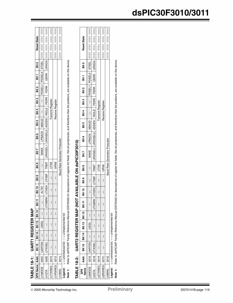
dsPIC30F3010/3011
TAB
LE
18-
1:U
AR
T1
RE
GIS
TE
R M
AP
TAB
LE
18-
2:U
AR
T2
RE
GIS
TE
R M
AP
(N
OT
AV
AIL
AB
LE
ON
dsP
IC30
F30
10)
SF
R N
ame
Ad
dr.
Bit
15
Bit
14
Bit
13
Bit
12
Bit
11
Bit
10
Bit
9B
it 8
Bit
7B
it 6
Bit
5B
it 4
Bit
3B
it 2
Bit
1B
it 0
Res
et S
tate
U1M
OD
E02
0CU
AR
TE
N—
US
IDL
——
ALT
IO—
—W
AK
ELP
BA
CK
AB
AU
D—
—P
DS
EL1
PD
SE
L0S
TS
EL
0000 0000 0000 0000
U1S
TA02
0EU
TX
ISE
L—
——
UT
XB
RK
UT
XE
NU
TX
BF
TR
MT
UR
XIS
EL1
UR
XIS
EL0
AD
DE
NR
IDLE
PE
RR
FE
RR
OE
RR
UR
XD
A0000 0001 0001 0000
U1T
XR
EG
0210
——
——
——
—U
TX
8Tr
ansm
it R
egis
ter
0000 000u uuuu uuuu
U1R
XR
EG
0212
——
——
——
—U
RX
8R
ecei
ve R
egis
ter
0000 0000 0000 0000
U1B
RG
0214
Bau
d R
ate
Gen
erat
or P
resc
aler
0000 0000 0000 0000
Leg
end
:u
= u
nini
tializ
ed b
it; —
= u
nim
plem
ente
d bi
t
No
te1:
Ref
er to
dsP
IC30
F F
amily
Ref
eren
ce M
anua
l (D
S70
046)
for
desc
riptio
ns o
f reg
iste
r bi
t fie
lds.
Not
all
perip
hera
ls, a
nd th
eref
ore
thei
r bi
t pos
ition
s, a
re a
vaila
ble
on th
is d
evic
e.
SF
R
Nam
eA
dd
r.B
it 1
5B
it 1
4B
it 1
3B
it 1
2B
it 1
1B
it 1
0B
it 9
Bit
8B
it 7
Bit
6B
it 5
Bit
4B
it 3
Bit
2B
it 1
Bit
0R
eset
Sta
te
U2M
OD
E02
16U
AR
TE
N—
US
IDL
——
——
—W
AK
ELP
BA
CK
AB
AU
D—
—P
DS
EL1
PD
SE
L0S
TS
EL
0000 0000 0000 0000
U2S
TA02
18U
TX
ISE
L—
——
UT
XB
RK
UT
XE
NU
TX
BF
TR
MT
UR
XIS
EL1
UR
XIS
EL0
AD
DE
NR
IDLE
PE
RR
FE
RR
OE
RR
UR
XD
A0000 0001 0001 0000
U2T
XR
EG
021A
——
——
——
—U
TX
8T
rans
mit
Reg
iste
r0000 000u uuuu uuuu
U2R
XR
EG
021C
——
——
——
—U
RX
8R
ecei
ve R
egis
ter
0000 0000 0000 0000
U2B
RG
021E
Bau
d R
ate
Gen
erat
or P
resc
aler
0000 0000 0000 0000
Leg
end
:u
= u
nini
tializ
ed b
it; —
= u
nim
plem
ente
d bi
t
No
te1:
Ref
er to
dsP
IC30
F F
amily
Ref
eren
ce M
anua
l (D
S70
046)
for
desc
riptio
ns o
f reg
iste
r bi
t fie
lds.
Not
all
perip
hera
ls, a
nd th
eref
ore
thei
r bi
t pos
ition
s, a
re a
vaila
ble
on th
is d
evic
e.
© 2005 Microchip Technology Inc. Preliminary DS70141B-page 119

dsPIC30F3010/3011
NOTES:
DS70141B-page 120 Preliminary © 2005 Microchip Technology Inc.
dsPIC30F3010/3011
19.0 10-BIT HIGH SPEED ANALOG-TO-DIGITAL CONVERTER (A/D) MODULE
The10-bit high-speed analog-to-digital converter (A/D)allows conversion of an analog input signal to a 10-bitdigital number. This module is based on a SuccessiveApproximation Register (SAR) architecture, and providesa maximum sampling rate of 500 ksps. The A/D modulehas 16 analog inputs which are multiplexed into foursample and hold amplifiers. The output of the sample andhold is the input into the converter, which generates theresult. The analog reference voltages are softwareselectable to either the device supply voltage (AVDD/AVSS) or the voltage level on the (VREF+/VREF-) pin. TheA/D converter has a unique feature of being able tooperate while the device is in Sleep mode.
The A/D module has six 16-bit registers:
• A/D Control register1 (ADCON1)• A/D Control register2 (ADCON2)
• A/D Control register3 (ADCON3)• A/D Input Select register (ADCHS)• A/D Port Configuration register (ADPCFG)
• A/D Input Scan Selection register (ADCSSL)
The ADCON1, ADCON2 and ADCON3 registerscontrol the operation of the A/D module. The ADCHSregister selects the input channels to be converted. TheADPCFG register configures the port pins as analoginputs or as digital I/O. The ADCSSL register selectsinputs for scanning.
The block diagram of the A/D module is shown inFigure 19-1.
Note: This data sheet summarizes features of this groupof dsPIC30F devices and is not intended to be a completereference source. For more information on the CPU,peripherals, register descriptions and general devicefunctionality, refer to the dsPIC30F Family ReferenceManual (DS70046).
Note: The SSRC<2:0>, ASAM, SIMSAM,SMPI<3:0>, BUFM and ALTS bits, as wellas the ADCON3 and ADCSSL registers,must not be written to while ADON = 1.This would lead to indeterminate results.
© 2005 Microchip Technology Inc. Preliminary DS70141B-page 121

dsPIC30F3010/3011
FIGURE 19-1: 10-BIT HIGH SPEED A/D FUNCTIONAL BLOCK DIAGRAM
S/H
+
-
10-bit Result Conversion Logic
VREF+
AVSSAVDD
ADC
Dat
a
16-word, 10-bitDual Port
Buffer
Bus
Inte
rfac
e
AN0
AN5
AN7
AN1AN2AN3
AN4
AN6
AN8*AN8
AN4
AN5
*AN6
*AN7
AN0
AN1
AN2
AN3
CH1
CH2
CH3
CH0
AN5AN2
AN8
AN4AN1
AN7
AN3AN0
AN6
AN1
VREF-
Sample/SequenceControlsample
CH1,CH2,CH3,CH0
Input MuxControl
inputswitches
S/H
+
-
S/H
+
-
S/H
+
-
For
mat
* = Not available on dsPIC30F3010.
DS70141B-page 122 Preliminary © 2005 Microchip Technology Inc.

dsPIC30F3010/3011
19.1 A/D Result Buffer
The module contains a 16-word dual port read-onlybuffer, called ADCBUF0...ADCBUFF, to buffer the A/Dresults. The RAM is 10 bits wide, but is read into differentformat 16-bit words. The contents of the sixteen A/Dconversion result buffer registers, ADCBUF0 throughADCBUFF, cannot be written by user software.
19.2 Conversion Operation
After the A/D module has been configured, the sampleacquisition is started by setting the SAMP bit. Varioussources, such as a programmable bit, timer time-outs andexternal events, will terminate acquisition and start a con-version. When the A/D conversion is complete, the resultis loaded into ADCBUF0...ADCBUFF, and the A/Dinterrupt flag ADIF and the DONE bit are set after thenumber of samples specified by the SMPI bit.
The following steps should be followed for doing anA/D conversion:
• Configure the A/D module:- Configure analog pins, voltage reference and
digital I/O- Select A/D input channels
- Select A/D conversion clock- Select A/D conversion trigger- Turn on A/D module
• Configure A/D interrupt (if required):- Clear ADIF bit - Select A/D interrupt priority
• Start sampling• Wait the required acquisition time• Trigger acquisition end; start conversion
• Wait for A/D conversion to complete, by either:- Waiting for the A/D interrupt
• Read A/D result buffer; clear ADIF if required
19.3 Selecting the Conversion Sequence
Several groups of control bits select the sequence inwhich the A/D connects inputs to the sample/holdchannels, converts channels, writes the buffer memory,and generates interrupts. The sequence is controlledby the sampling clocks.
The SIMSAM bit controls the acquire/convertsequence for multiple channels. If the SIMSAM bit is‘0’, the two or four selected channels are acquired andconverted sequentially, with two or four sample clocks.If the SIMSAM bit is ‘1’, two or four selected channelsare acquired simultaneously, with one sample clock.The channels are then converted sequentially. Obvi-ously, if there is only 1 channel selected, the SIMSAMbit is not applicable.
The CHPS bits selects how many channels are sam-pled. This can vary from 1, 2 or 4 channels. If CHPSselects 1 channel, the CH0 channel will be sampled atthe sample clock and converted. The result is stored inthe buffer. If CHPS selects 2 channels, the CH0 andCH1 channels will be sampled and converted. If CHPSselects 4 channels, the CH0, CH1, CH2 and CH3channels will be sampled and converted.
The SMPI bits select the number of acquisition/conver-sion sequences that would be performed before aninterrupt occurs. This can vary from 1 sample perinterrupt to 16 samples per interrupt.
The user cannot program a combination of CHPS andSMPI bits that specifies more than 16 conversions perinterrupt, or 8 conversions per interrupt, depending onthe BUFM bit. The BUFM bit, when set, will split the16-word results buffer (ADCBUF0...ADCBUFF) intotwo 8-word groups. Writing to the 8-word buffers will bealternated on each interrupt event. Use of the BUFM bitwill depend on how much time is available for movingdata out of the buffers after the interrupt, as determinedby the application.
If the processor can quickly unload a full buffer withinthe time it takes to acquire and convert one channel,the BUFM bit can be ‘0’ and up to 16 conversions maybe done per interrupt. The processor will have onesample and conversion time to move the sixteenconversions.
If the processor cannot unload the buffer within theacquisition and conversion time, the BUFM bit shouldbe ‘1’. For example, if SMPI<3:0> (ADCON2<5:2>) =0111, then eight conversions will be loaded into 1/2 ofthe buffer, following which an interrupt occurs. The nexteight conversions will be loaded into the other 1/2 of thebuffer. The processor will have the entire time betweeninterrupts to move the eight conversions.
The ALTS bit can be used to alternate the inputsselected during the sampling sequence. The inputmultiplexer has two sets of sample inputs: MUX A andMUX B. If the ALTS bit is ‘0’, only the MUX A inputs areselected for sampling. If the ALTS bit is ‘1’ andSMPI<3:0> = 0000, on the first sample/convertsequence, the MUX A inputs are selected, and on thenext acquire/convert sequence, the MUX B inputs areselected.
The CSCNA bit (ADCON2<10>) will allow the CH0channel inputs to be alternately scanned across aselected number of analog inputs for the MUX A group.The inputs are selected by the ADCSSL register. If aparticular bit in the ADCSSL register is ‘1’, the corre-sponding input is selected. The inputs are alwaysscanned from lower to higher numbered inputs, startingafter each interrupt. If the number of inputs selected isgreater than the number of samples taken per interrupt,the higher numbered inputs are unused.
© 2005 Microchip Technology Inc. Preliminary DS70141B-page 123
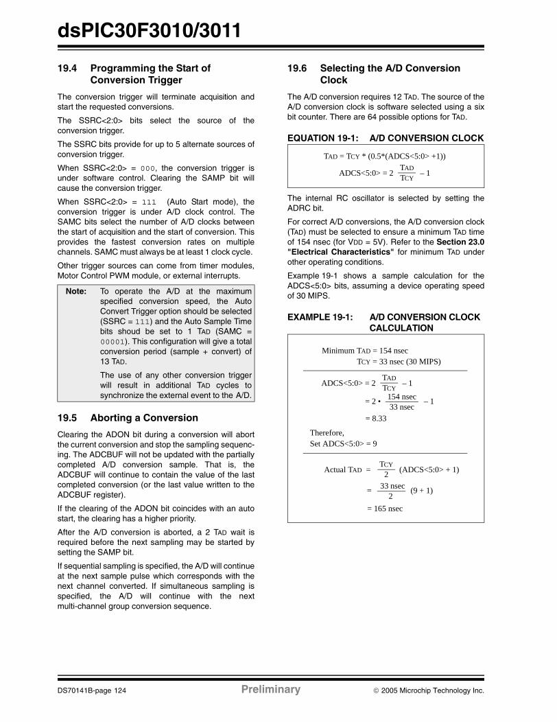
dsPIC30F3010/3011
19.4 Programming the Start of Conversion Trigger
The conversion trigger will terminate acquisition andstart the requested conversions.
The SSRC<2:0> bits select the source of theconversion trigger.
The SSRC bits provide for up to 5 alternate sources ofconversion trigger.
When SSRC<2:0> = 000, the conversion trigger isunder software control. Clearing the SAMP bit willcause the conversion trigger.
When SSRC<2:0> = 111 (Auto Start mode), theconversion trigger is under A/D clock control. TheSAMC bits select the number of A/D clocks betweenthe start of acquisition and the start of conversion. Thisprovides the fastest conversion rates on multiplechannels. SAMC must always be at least 1 clock cycle.
Other trigger sources can come from timer modules,Motor Control PWM module, or external interrupts.
19.5 Aborting a Conversion
Clearing the ADON bit during a conversion will abortthe current conversion and stop the sampling sequenc-ing. The ADCBUF will not be updated with the partiallycompleted A/D conversion sample. That is, theADCBUF will continue to contain the value of the lastcompleted conversion (or the last value written to theADCBUF register).
If the clearing of the ADON bit coincides with an autostart, the clearing has a higher priority.
After the A/D conversion is aborted, a 2 TAD wait isrequired before the next sampling may be started bysetting the SAMP bit.
If sequential sampling is specified, the A/D will continueat the next sample pulse which corresponds with thenext channel converted. If simultaneous sampling isspecified, the A/D will continue with the nextmulti-channel group conversion sequence.
19.6 Selecting the A/D Conversion Clock
The A/D conversion requires 12 TAD. The source of theA/D conversion clock is software selected using a sixbit counter. There are 64 possible options for TAD.
EQUATION 19-1: A/D CONVERSION CLOCK
The internal RC oscillator is selected by setting theADRC bit.
For correct A/D conversions, the A/D conversion clock(TAD) must be selected to ensure a minimum TAD timeof 154 nsec (for VDD = 5V). Refer to the Section 23.0"Electrical Characteristics" for minimum TAD underother operating conditions.
Example 19-1 shows a sample calculation for theADCS<5:0> bits, assuming a device operating speedof 30 MIPS.
EXAMPLE 19-1: A/D CONVERSION CLOCK CALCULATION
Note: To operate the A/D at the maximumspecified conversion speed, the AutoConvert Trigger option should be selected(SSRC = 111) and the Auto Sample Timebits shoud be set to 1 TAD (SAMC =00001). This configuration will give a totalconversion period (sample + convert) of13 TAD.
The use of any other conversion triggerwill result in additional TAD cycles tosynchronize the external event to the A/D.
TAD = TCY * (0.5*(ADCS<5:0> +1))
ADCS<5:0> = 2 – 1TAD
TCY
Minimum TAD = 154 nsec
ADCS<5:0> = 2 – 1TAD
TCY
TCY = 33 nsec (30 MIPS)
= 2 • – 1154 nsec33 nsec
= 8.33
Therefore,Set ADCS<5:0> = 9
Actual TAD = (ADCS<5:0> + 1)TCY
2
= (9 + 1)33 nsec
2
= 165 nsec
DS70141B-page 124 Preliminary © 2005 Microchip Technology Inc.

dsPIC30F3010/3011
19.7 A/D Acquisition Requirements
The analog input model of the 10-bit A/D converter isshown in Figure 19-2. The total sampling time for theA/D is a function of the internal amplifier settling time,device VDD and the holding capacitor charge time.
For the A/D converter to meet its specified accuracy,the charge holding capacitor (CHOLD) must be allowedto fully charge to the voltage level on the analog inputpin. The source impedance (RS), the interconnectimpedance (RIC) and the internal sampling switch(RSS) impedance combine to directly affect the timerequired to charge the capacitor CHOLD. The combinedimpedance of the analog sources must therefore besmall enough to fully charge the holding capacitorwithin the chosen sample time. To minimize the effectsof pin leakage currents on the accuracy of the A/Dconverter, the maximum recommended source imped-ance, RS, is 5 kΩ. After the analog input channel isselected (changed), this sampling function must becompleted prior to starting the conversion. The internalholding capacitor will be in a discharged state prior toeach sample operation.
The user must allow at least 1 TAD period of samplingtime, TSAMP, between conversions to allow eachsample to be acquired. This sample time may becontrolled manually in software by setting/clearing theSAMP bit, or it may be automatically controlled by theA/D converter. In an automatic configuration, the usermust allow enough time between conversion triggersso that the minimum sample time can be satisfied.Refer to the Section 23.0 "ElectricalCharacteristics" for TAD and sample timerequirements.
FIGURE 19-2: A/D CONVERTER ANALOG INPUT MODEL
CPINVA
Rs ANxVT = 0.6V
VT = 0.6V I leakage
RIC ≤ 250Ω SamplingSwitch
RSS
CHOLD= DAC capacitance
VSS
VDD
= 4.4 pF± 500 nA
Legend: CPIN
VT
I leakage
RIC
RSS
CHOLD
= input capacitance= threshold voltage= leakage current at the pin due to
= interconnect resistance= sampling switch resistance= sample/hold capacitance (from DAC)
various junctions
Note: CPIN value depends on device package and is not tested. Effect of CPIN negligible if Rs ≤ 5 kΩ.
RSS ≤ 3 kΩ
© 2005 Microchip Technology Inc. Preliminary DS70141B-page 125

dsPIC30F3010/3011
19.8 Module Power-down Modes
The module has 3 internal power modes. When theADON bit is ‘1’, the module is in Active mode; it is fullypowered and functional. When ADON is ‘0’, the moduleis in Off mode. The digital and analog portions of thecircuit are disabled for maximum current savings. Inorder to return to the Active mode from Off mode, theuser must wait for the ADC circuitry to stabilize.
19.9 A/D Operation During CPU Sleep and Idle Modes
19.9.1 A/D OPERATION DURING CPU SLEEP MODE
When the device enters Sleep mode, all clock sourcesto the module are shutdown and stay at logic ‘0’.
If Sleep occurs in the middle of a conversion, theconversion is aborted. The converter will not continuewith a partially completed conversion on exit fromSleep mode.
Register contents are not affected by the deviceentering or leaving Sleep mode.
The A/D module can operate during Sleep mode if theA/D clock source is set to RC (ADRC = 1). When theRC clock source is selected, the A/D module waits oneinstruction cycle before starting the conversion. Thisallows the SLEEP instruction to be executed, whicheliminates all digital switching noise from the conver-sion. When the conversion is complete, the Done bitwill be set and the result loaded into the ADCBUFregister.
If the A/D interrupt is enabled, the device will wake-upfrom Sleep. If the A/D interrupt is not enabled, the A/Dmodule will then be turned off, although the ADON bitwill remain set.
19.9.2 A/D OPERATION DURING CPU IDLE MODE
The ADSIDL bit selects if the module will stop on Idle orcontinue on Idle. If ADSIDL = 0, the module willcontinue operation on assertion of Idle mode. IfADSIDL = 1, the module will stop on Idle.
19.10 Effects of a Reset
A device Reset forces all registers to their Reset state.This forces the A/D module to be turned off, and anyconversion and acquisition sequence is aborted. Thevalues that are in the ADCBUF registers are notmodified. The A/D result register will contain unknowndata after a Power-on Reset.
19.11 Output Formats
The A/D result is 10-bits wide. The data buffer RAM isalso 10-bits wide. The 10-bit data can be read in one offour different formats. The FORM<1:0> bits select theformat. Each of the output formats translates to a 16-bitresult on the data bus.
Write data will always be in right justified (integer)format.
FIGURE 19-3: A/D OUTPUT DATA FORMATS
RAM Contents: d09 d08 d07 d06 d05 d04 d03 d02 d01 d00
Read to Bus:
Signed Fractional (1.15) d09 d08 d07 d06 d05 d04 d03 d02 d01 d00 0 0 0 0 0 0
Fractional (1.15) d09 d08 d07 d06 d05 d04 d03 d02 d01 d00 0 0 0 0 0 0
Signed Integer d09 d09 d09 d09 d09 d09 d09 d08 d07 d06 d05 d04 d03 d02 d01 d00
Integer 0 0 0 0 0 0 d09 d08 d07 d06 d05 d04 d03 d02 d01 d00
DS70141B-page 126 Preliminary © 2005 Microchip Technology Inc.

dsPIC30F3010/3011
19.12 Configuring Analog Port Pins
The use of the ADPCFG and TRIS registers control theoperation of the A/D port pins. The port pins that aredesired as analog inputs must have their correspond-ing TRIS bit set (input). If the TRIS bit is cleared(output), the digital output level (VOH or VOL) will beconverted.
The A/D operation is independent of the state of theCH0SA<3:0>/CH0SB<3:0> bits and the TRIS bits.
When reading the PORT register, all pins configured asanalog input channels will read as cleared.
Pins configured as digital inputs will not convert ananalog input. Analog levels on any pin that is defined asa digital input (including the ANx pins) may cause theinput buffer to consume current that exceeds thedevice specifications.
19.13 Connection Considerations
The analog inputs have diodes to VDD and VSS as ESDprotection. This requires that the analog input bebetween VDD and VSS. If the input voltage exceeds thisrange by greater than 0.3V (either direction), one of thediodes becomes forward biased and it may damage thedevice if the input current specification is exceeded.
An external RC filter is sometimes added for anti-aliasing of the input signal. The R component should beselected to ensure that the sampling time requirementsare satisfied. Any external components connected (viahigh impedance) to an analog input pin (capacitor,zener diode, etc.) should have very little leakagecurrent at the pin.
© 2005 Microchip Technology Inc. Preliminary DS70141B-page 127

dsPIC30F3010/3011
TABL
E 1
9-1:
AD
C R
EG
IST
ER
MA
PS
FR
Nam
eA
dd
r.B
it 1
5B
it 1
4B
it 1
3B
it 1
2B
it 1
1B
it 1
0B
it 9
Bit
8B
it 7
Bit
6B
it 5
Bit
4B
it 3
Bit
2B
it 1
Bit
0R
eset
Sta
te
AD
CB
UF
002
80—
——
——
—A
DC
Dat
a B
uffe
r 0
0000 00uu uuuu uuuu
AD
CB
UF
102
82—
——
——
—A
DC
Dat
a B
uffe
r 1
0000 00uu uuuu uuuu
AD
CB
UF
202
84—
——
——
—A
DC
Dat
a B
uffe
r 2
0000 00uu uuuu uuuu
AD
CB
UF
302
86—
——
——
—A
DC
Dat
a B
uffe
r 3
0000 00uu uuuu uuuu
AD
CB
UF
402
88—
——
——
—A
DC
Dat
a B
uffe
r 4
0000 00uu uuuu uuuu
AD
CB
UF
502
8A—
——
——
—A
DC
Dat
a B
uffe
r 5
0000 00uu uuuu uuuu
AD
CB
UF
602
8C—
——
——
—A
DC
Dat
a B
uffe
r 6
0000 00uu uuuu uuuu
AD
CB
UF
702
8E—
——
——
—A
DC
Dat
a B
uffe
r 7
0000 00uu uuuu uuuu
AD
CB
UF
802
90—
——
——
—A
DC
Dat
a B
uffe
r 8
0000 00uu uuuu uuuu
AD
CB
UF
902
92—
——
——
—A
DC
Dat
a B
uffe
r 9
0000 00uu uuuu uuuu
AD
CB
UFA
0294
——
——
——
AD
C D
ata
Buf
fer
100000 00uu uuuu uuuu
AD
CB
UF
B02
96—
——
——
—A
DC
Dat
a B
uffe
r 11
0000 00uu uuuu uuuu
AD
CB
UF
C02
98—
——
——
—A
DC
Dat
a B
uffe
r 12
0000 00uu uuuu uuuu
AD
CB
UF
D02
9A—
——
——
—A
DC
Dat
a B
uffe
r 13
0000 00uu uuuu uuuu
AD
CB
UF
E02
9C—
——
——
—A
DC
Dat
a B
uffe
r 14
0000 00uu uuuu uuuu
AD
CB
UF
F02
9E—
——
——
—A
DC
Dat
a B
uffe
r 15
0000 00uu uuuu uuuu
AD
CO
N1
02A
0A
DO
N—
AD
SID
L—
——
FO
RM
<1:
0>S
SR
C<
2:0>
—S
IMS
AM
AS
AM
SA
MP
DO
NE
0000 0000 0000 0000
AD
CO
N2
02A
2V
CF
G<
2:0>
——
CS
CN
AC
HP
S<
1:0>
BU
FS
—S
MP
I<3:
0>B
UF
MA
LTS
0000 0000 0000 0000
AD
CO
N3
02A
4—
——
SA
MC
<4:
0>A
DR
C—
AD
CS
<5:
0>0000 0000 0000 0000
AD
CH
S02
A6
CH
123N
B<
1:0>
CH
123S
BC
H0N
BC
H0S
B<
3:0>
CH
123N
A<
1:0>
CH
123S
AC
H0N
AC
H0S
A<
3:0>
0000 0000 0000 0000
AD
PC
FG
02A
8—
——
——
——
PC
FG
8*P
CF
G7*
PC
FG
6*P
CF
G5
PC
FG
4P
CF
G3
PC
FG
2P
CF
G1
PC
FG
00000 0000 0000 0000
AD
CS
SL
02A
A—
——
——
——
CS
SL8
*C
SS
L7*
CS
SL6
*C
SS
L5C
SS
L4C
SS
L3C
SS
L2C
SS
L1C
SS
L00000 0000 0000 0000
Leg
end
:u
= u
nini
tializ
ed b
it; —
= u
nim
plem
ente
d bi
t, *
= n
ot a
vaila
ble
on d
sPIC
30F
3010
No
te1:
Ref
er to
dsP
IC30
F F
amily
Ref
eren
ce M
anua
l (D
S70
046)
for
desc
riptio
ns o
f reg
iste
r bi
t fie
lds.
Not
all
perip
hera
ls, a
nd th
eref
ore
thei
r bi
t pos
ition
s, a
re a
vaila
ble
on th
is d
evic
e.
DS70141B-page 128 Preliminary © 2005 Microchip Technology Inc.

dsPIC30F3010/3011
20.0 SYSTEM INTEGRATION
There are several features intended to maximizesystem reliability, minimize cost through elimination ofexternal components, provide power saving operatingmodes and offer code protection:
• Oscillator Selection• Reset
- Power-on Reset (POR)
- Power-up Timer (PWRT)- Oscillator Start-up Timer (OST)- Programmable Brown-out Reset (BOR)
• Watchdog Timer (WDT)• Power Saving modes (Sleep and Idle)• Code Protection
• Unit ID Locations• In-Circuit Serial Programming™ (ICSP™)
dsPIC30F devices have a Watchdog Timer, which ispermanently enabled via the configuration bits, or canbe software controlled. It runs off its own RC oscillatorfor added reliability. There are two timers that offer nec-essary delays on power-up. One is the Oscillator Start-up Timer (OST), intended to keep the chip in Reset untilthe crystal oscillator is stable. The other is the Power-up Timer (PWRT), which provides a delay on power-uponly, designed to keep the part in Reset while thepower supply stabilizes. With these two timers on-chip,most applications need no external Reset circuitry.
Sleep mode is designed to offer a very low currentPower-down mode. The user can wake-up from Sleepthrough external Reset, Watchdog Timer Wake-up orthrough an interrupt. Several oscillator options are alsomade available to allow the part to fit a wide variety ofapplications. In the Idle mode, the clock sources arestill active, but the CPU is shut-off. The RC oscillatoroption saves system cost, while the LP crystal optionsaves power.
20.1 Oscillator System Overview
The dsPIC30F oscillator system has the followingmodules and features:
• Various external and internal oscillator options as clock sources
• An on-chip PLL to boost internal operating frequency
• A clock switching mechanism between various clock sources
• Programmable clock postscaler for system power savings
• A Fail-Safe Clock Monitor (FSCM) that detects clock failure and takes fail-safe measures
• Clock Control register OSCCON• Configuration bits for main oscillator selection
Configuration bits determine the clock source uponPower-on Reset (POR) and Brown-out Reset (BOR).Thereafter, the clock source can be changed betweenpermissible clock sources. The OSCCON registercontrols the clock switching and reflects system clockrelated status bits.
Table 20-1 provides a summary of the dsPIC30FOscillator Operating modes. A simplified diagram of theoscillator system is shown in Figure 20-1.
Note: This data sheet summarizes features of this groupof dsPIC30F devices and is not intended to be a completereference source. For more information on the CPU,peripherals, register descriptions and general devicefunctionality, refer to the dsPIC30F Family ReferenceManual (DS70046). For more information on the deviceinstruction set and programming, refer to the dsPIC30FProgrammer’s Reference Manual (DS70030).
© 2005 Microchip Technology Inc. Preliminary DS70141B-page 129

dsPIC30F3010/3011
TABLE 20-1: OSCILLATOR OPERATING MODES
Oscillator Mode Description
XTL 200 kHz-4 MHz crystal on OSC1:OSC2.
XT 4 MHz-10 MHz crystal on OSC1:OSC2.
XT w/ PLL 4x 4 MHz-10 MHz crystal on OSC1:OSC2, 4x PLL enabled.
XT w/ PLL 8x 4 MHz-10 MHz crystal on OSC1:OSC2, 8x PLL enabled.
XT w/ PLL 16x 4 MHz-10 MHz crystal on OSC1:OSC2, 16x PLL enabled(1).
LP 32 kHz crystal on SOSCO:SOSCI(2).
HS 10 MHz-25 MHz crystal.
HS/2 w/PLL 4x 10 MHz -25 MHz crystal, divide by 2, 4x PLL enabled.
HS/2 w/ PLL 8x 10 MHz-25MHz crystal, divide by 2, 8x PLL enabled.
HS/2 w/ PLL 16x 10 MHz-25MHz crystal, divide by 2, 16x PLL enabled(1).
HS/3 w/PLL 4x 10 MHz-25 MHz crystal, divide by 3, 4x PLL enabled.
HS/3 w/ PLL 8x 10 MHz-25MHz crystal, divide by 3, 8x PLL enabled.
HS/3 w/ PLL 16x 10 MHz-25MHz crystal, divide by 3, 16x PLL enabled(1).
EC External clock input (0-40 MHz).
ECIO External clock input (0-40 MHz), OSC2 pin is I/O.
EC w/ PLL 4x External clock input (4-10 MHz), OSC2 pin is I/O, 4x PLL enabled(1).
EC w/ PLL 8x External clock input (4-10 MHz), OSC2 pin is I/O, 8x PLL enabled(1).
EC w/ PLL 16x External clock input (4-10 MHz), OSC2 pin is I/O, 16x PLL enabled(1).
ERC External RC oscillator, OSC2 pin is FOSC/4 output(3).
ERCIO External RC oscillator, OSC2 pin is I/O(3).
FRC 8 MHz internal RC oscillator.
FRC w/ PLL 4x 8 MHz Internal RC oscillator, 4x PLL enabled.
FRC w/ PLL 8x 8 MHz Internal RC oscillator, 8x PLL enabled.
FRC w/ PLL 16x 7.5 MHz Internal RC oscillator, 16x PLL enabled.
LPRC 512 kHz internal RC oscillator.
Note 1: dsPIC30F maximum operating frequency of 120 MHz must be met.
2: LP oscillator can be conveniently shared as system clock, as well as real-time clock for Timer1.3: Requires external R and C. Frequency operation up to 4 MHz.
DS70141B-page 130 Preliminary © 2005 Microchip Technology Inc.

dsPIC30F3010/3011
FIGURE 20-1: OSCILLATOR SYSTEM BLOCK DIAGRAM
Primary OSC1
OSC2
SOSCO
SOSCI
Oscillator
32 kHz LP
Clock
and Control
Block
Switching
Oscillator
x4, x8, x16
PLL
Primary
Oscillator
Stability Detector
Stability Detector
SecondaryOscillator
Programmable
Clock Divider
OscillatorStart-upTimer
Fail-Safe ClockMonitor (FSCM)
Internal Fast RCOscillator (FRC)
Internal LowPower RC
Oscillator (LPRC)
PWRSAV Instruction
Wake-up Request
Oscillator Configuration bits
SystemClock
Oscillator Trap
To Timer1
LPRC
Secondary Osc
POR Done
Primary Osc
FPLL
POST<1:0>
2
FCKSM<1:0>2
PLL
Lock COSC<2:0>
NOSC<2:0>
OSWEN
CF
TUN<3:0>4
© 2005 Microchip Technology Inc. Preliminary DS70141B-page 131

dsPIC30F3010/3011
20.2 Oscillator Configurations
20.2.1 INITIAL CLOCK SOURCE SELECTION
While coming out of Power-on Reset or Brown-outReset, the device selects its clock source based on:
a) FOS<2:0> configuration bits that select one offour oscillator groups,
b) and FPR<4:0> configuration bits that select oneof 15 oscillator choices within the primary group.
The selection is as shown in Table 20-2.
20.2.2 OSCILLATOR START-UP TIMER (OST)
In order to ensure that a crystal oscillator (or ceramicresonator) has started and stabilized, an oscillatorstart-up timer is included. It is a simple 10-bit counterthat counts 1024 TOSC cycles before releasing theoscillator clock to the rest of the system. The time-outperiod is designated as TOST. The TOST time is involvedevery time the oscillator has to restart (i.e., on POR,BOR and wake-up from Sleep). The oscillator start-uptimer is applied to the LP Oscillator, XT, XTL and HSmodes (upon wake-up from Sleep, POR and BOR) forthe primary oscillator.
TABLE 20-2: CONFIGURATION BIT VALUES FOR CLOCK SELECTION
Oscillator ModeOscillator
SourceFOS<2:0> FPR<4:0> OSC2 Function
ECIO w/ PLL 4x PLL 1 1 1 0 1 1 0 1 I/O
ECIO w/ PLL 8x PLL 1 1 1 0 1 1 1 0 I/O
ECIO w/ PLL 16x PLL 1 1 1 0 1 1 1 1 I/O
FRC w/ PLL 4X PLL 1 1 1 0 0 0 0 1 I/O
FRC w/ PLL 8x PLL 1 1 1 0 1 0 1 0 I/O
FRC w/ PLL 16x PLL 1 1 1 0 0 0 1 1 I/O
XT w/ PLL 4x PLL 1 1 1 0 0 1 0 1 OSC2
XT w/ PLL 8x PLL 1 1 1 0 0 1 1 0 OSC2
XT w/ PLL 16x PLL 1 1 1 0 0 1 1 1 OSC2
HS2 w/ PLL 4x PLL 1 1 1 1 0 0 0 1 OSC2
HS2 w/ PLL 8x PLL 1 1 1 1 0 0 1 0 OSC2
HS2 w/ PLL 16x PLL 1 1 1 1 0 0 1 1 OSC2
HS3 w/ PLL 4x PLL 1 1 1 1 0 1 0 1 OSC2
HS3 w/ PLL 8x PLL 1 1 1 1 0 1 1 0 OSC2
HS3 w/ PLL 16x PLL 1 1 1 1 0 1 1 1 OSC2
ECIO External 0 1 1 0 1 1 0 0 I/O
XT External 0 1 1 0 0 1 0 0 OSC2
HS External 0 1 1 0 0 0 1 0 OSC2
EC External 0 1 1 0 1 0 1 1 CLKOUT
ERC External 0 1 1 0 1 0 0 1 CLKOUT
ERCIO External 0 1 1 0 1 0 0 0 I/O
XTL External 0 1 1 0 0 0 0 0 OSC2
LP Secondary 0 0 0 X X X X X (Note 1, 2)
FRC Internal FRC 0 0 1 X X X X X (Note 1, 2)
LPRC Internal LPRC 0 1 0 X X X X X (Note 1, 2)
Note 1: OSC2 pin function is determined by (FPR<4:0>).2: OSC1 pin cannot be used as an I/O pin even if the secondary oscillator or an internal clock source is selected at all
times.
DS70141B-page 132 Preliminary © 2005 Microchip Technology Inc.

dsPIC30F3010/3011
20.2.3 LP OSCILLATOR CONTROL
Enabling the LP oscillator is controlled with twoelements:
1. The current oscillator group bits COSC<2:0>2. The LPOSCEN bit (OSCON register)
The LP oscillator is on (even during Sleep mode) ifLPOSCEN = 1. The LP oscillator is the device clock if:
• COSC<1:0> = 00 (LP selected as main oscillator) and
• LPOSCEN = 1
Keeping the LP oscillator on at all times allows for afast switch to the 32 kHz system clock for lower poweroperation. Returning to the faster main oscillator willstill require a start-up time.
20.2.4 PHASE LOCKED LOOP (PLL)
The PLL multiplies the clock which is generated by theprimary oscillator. The PLL is selectable to have eithergains of x4, x8, and x16. Input and output frequencyranges are summarized in Table 20-3.
TABLE 20-3: PLL FREQUENCY RANGE
The PLL features a lock output, which is asserted whenthe PLL enters a phase locked state. Should the loopfall out of lock (e.g., due to noise), the lock signal will berescinded. The state of this signal is reflected in theread only LOCK bit in the OSCCON register.
20.2.5 FAST RC OSCILLATOR (FRC)
The FRC oscillator is a fast (8 MHz nominal) internalRC oscillator. This oscillator is intended to providereasonable device operating speeds without the use ofan external crystal, ceramic resonator or RC network.The FRC oscillator can be used with the PLL to obtainhigher clock frequencies.
The dsPIC30F operates from the FRC oscillatorwhenever the Current Oscillator Selection control bitsin the OSCCON register (OSCCON<13:12>) are set to‘01’.
The four bit field specified by TUN<3:0>(OSCTUN<3:0>) allows the user to tune the internalfast RC oscillator (nominal 8.0 MHz). The user can tunethe FRC oscillator within a range of +10.5% (840 kHz)and -12% (960 kHz) in steps of 1.50% around thefactory-calibrated setting, see Table 20-4.
If OSCCON<14:12> are set to ‘111’ and FPR<4:0> areset to ‘00101’, ‘00110’ or ‘00111’, then a PLL multiplierof 4, 8 or 16 (respectively) is applied
.
TABLE 20-4: FRC TUNING
20.2.6 LOW-POWER RC OSCILLATOR (LPRC)
The LPRC oscillator is a component of the WatchdogTimer (WDT) and oscillates at a nominal frequency of512 kHz. The LPRC oscillator is the clock source forthe Power-up Timer (PWRT) circuit, WDT and clockmonitor circuits. It may also be used to provide a lowfrequency clock source option for applications wherepower consumption is critical, and timing accuracy isnot required.
The LPRC oscillator is always enabled at a Power-onReset, because it is the clock source for the PWRT.After the PWRT expires, the LPRC oscillator will remainON if one of the following is TRUE:
• The Fail-Safe Clock Monitor is enabled
• The WDT is enabled• The LPRC oscillator is selected as the system
clock via the COSC<1:0> control bits in the OSCCON register
If one of the above conditions is not true, the LPRC willshut-off after the PWRT expires.
FinPLL
MultiplierFout
4 MHz-10 MHz x4 16 MHz-40 MHz4 MHz-10 MHz x8 32 MHz-80 MHz
4 MHz-7.5 MHz x16 64 MHz-120 MHz
Note: When a 16x PLL is used, the FRC fre-quency must not be tuned to a frequencygreater than 7.5 MHz.
TUN<3:0>Bits
FRC Frequency
0111 + 10.5%0110 + 9.0%0101 + 7.5%0100 + 6.0%0011 + 4.5%0010 + 3.0%0001 + 1.5%0000 Center Frequency (oscillator is
running at calibrated frequency)1111 - 1.5%1110 - 3.0%1101 - 4.5%1100 - 6.0%1011 - 7.5%1010 - 9.0%1001 - 10.5%1000 - 12.0%
Note 1: OSC2 pin function is determined by thePrimary Oscillator mode selection(FPR<4:0>).
2: OSC1 pin cannot be used as an I/O pin,even if the secondary oscillator or aninternal clock source is selected at alltimes.
© 2005 Microchip Technology Inc. Preliminary DS70141B-page 133

dsPIC30F3010/3011
20.2.7 FAIL-SAFE CLOCK MONITOR
The Fail-Safe Clock Monitor (FSCM) allows the deviceto continue to operate even in the event of an oscillatorfailure. The FSCM function is enabled by appropriatelyprogramming the FCKSM configuration bits (ClockSwitch and Monitor Selection bits) in the FOSC DeviceConfiguration register. If the FSCM function isenabled, the LPRC Internal oscillator will run at alltimes (except during Sleep mode) and will not besubject to control by the SWDTEN bit.
In the event of an oscillator failure, the FSCM willgenerate a Clock Failure Trap event and will switch thesystem clock over to the FRC oscillator. The user willthen have the option to either attempt to restart theoscillator or execute a controlled shutdown. The usermay decide to treat the Trap as a warm Reset by simplyloading the Reset address into the oscillator fail trapvector. In this event, the CF (Clock Fail) status bit(OSCCON<3>) is also set whenever a clock failure isrecognized.
In the event of a clock failure, the WDT is unaffectedand continues to run on the LPRC clock.
If the oscillator has a very slow start-up time comingout of POR, BOR or Sleep, it is possible that thePWRT timer will expire before the oscillator hasstarted. In such cases, the FSCM will be activated andthe FSCM will initiate a clock failure trap, and theCOSC<1:0> bits are loaded with FRC oscillator selec-tion. This will effectively shut-off the original oscillatorthat was trying to start.
The user may detect this situation and restart theoscillator in the clock fail trap ISR.
Upon a clock failure detection, the FSCM module willinitiate a clock switch to the FRC Oscillator as follows:
1. The COSC bits (OSCCON<13:12>) are loadedwith the FRC Oscillator selection value.
2. CF bit is set (OSCCON<3>).
3. OSWEN control bit (OSCCON<0>) is cleared.
For the purpose of clock switching, the clock sourcesare sectioned into four groups:
1. Primary
2. Secondary3. Internal FRC4. Internal LPRC
The user can switch between these functional groups,but cannot switch between options within a group. If theprimary group is selected, then the choice within thegroup is always determined by the FPR<4:0>configuration bits.
The OSCCON register holds the control and status bitsrelated to clock switching.
• COSC<1:0>: Read only status bits always reflect the current oscillator group in effect.
• NOSC<2:0>: Control bits which are written to indicate the new oscillator group of choice.
- On POR and BOR, COSC<1:0> and NOSC<1:0> are both loaded with the configuration bit values FOS<1:0>.
• LOCK: The LOCK status bit indicates a PLL lock.
• CF: Read only status bit indicating if a clock fail detect has occurred.
• OSWEN: Control bit changes from a ‘0’ to a ‘1’ when a clock transition sequence is initiated. Clearing the OSWEN control bit will abort a clock transition in progress (used for hang-up situations).
If configuration bits FCKSM<1:0> = 1x, then the clockswitching and fail-safe clock monitor functions aredisabled. This is the default configuration bit setting.
If clock switching is disabled, then the FOS<1:0> andFPR<3:0> bits directly control the oscillator selectionand the COSC<1:0> bits do not control the clockselection. However, these bits will reflect the clocksource selection.
20.2.8 PROTECTION AGAINST ACCIDENTAL WRITES TO OSCCON
A write to the OSCCON register is intentionally madedifficult because it controls clock switching and clockscaling.
To write to the OSCCON low byte, the following codesequence must be executed without any otherinstructions in between:
Byte Write is allowed for one instruction cycle. Write thedesired value or use bit manipulation instruction.
To write to the OSCCON high byte, the followinginstructions must be executed without any otherinstructions in between::
Byte Write is allowed for one instruction cycle. Write thedesired value or use bit manipulation instruction.
Note: The application should not attempt toswitch to a clock of frequency lower than100 kHz when the fail-safe clock monitor isenabled. If such clock switching isperformed, the device may generate anoscillator fail trap and switch to the fast RCoscillator.
Byte Write “0x46” to OSCCON lowByte Write “0x57” to OSCCON low
Byte Write “0x78” to OSCCON highByte Write “0x9A” to OSCCON high
DS70141B-page 134 Preliminary © 2005 Microchip Technology Inc.

dsPIC30F3010/3011
20.3 Reset
The dsPIC30F3010/3011 differentiates between variouskinds of Reset:
a) Power-on Reset (POR) b) MCLR Reset during normal operation
c) MCLR Reset during Sleep d) Watchdog Timer (WDT) Reset (during normal
operation)e) Programmable Brown-out Reset (BOR) f) RESET Instruction
g) Reset cause by trap lockup (TRAPR)h) Reset caused by illegal opcode, or by using an
uninitialized W register as an address pointer(IOPUWR)
Different registers are affected in different ways byvarious Reset conditions. Most registers are notaffected by a WDT wake-up, since this is viewed as theresumption of normal operation. Status bits from theRCON register are set or cleared differently in differentReset situations, as indicated in Table 20-5. These bitsare used in software to determine the nature of theReset.
A block diagram of the on-chip Reset circuit is shown inFigure 20-2.
A MCLR noise filter is provided in the MCLR Resetpath. The filter detects and ignores small pulses.
Internally generated Resets do not drive MCLR pin low.
FIGURE 20-2: RESET SYSTEM BLOCK DIAGRAM
20.3.1 POR: POWER-ON RESET
A power-on event will generate an internal POR pulsewhen a VDD rise is detected. The Reset pulse will occurat the POR circuit threshold voltage (VPOR), which isnominally 1.85V. The device supply voltagecharacteristics must meet specified starting voltageand rise rate requirements. The POR pulse will reset aPOR timer and place the device in the Reset state. ThePOR also selects the device clock source identified bythe oscillator configuration fuses.
The POR circuit inserts a small delay, TPOR, which isnominally 10 μs and ensures that the device biascircuits are stable. Furthermore, a user selected power-up time-out (TPWRT) is applied. The TPWRT parameteris based on device configuration bits and can be 0 ms(no delay), 4 ms, 16 ms or 64 ms. The total delay is atdevice power-up TPOR + TPWRT. When these delayshave expired, SYSRST will be negated on the nextleading edge of the Q1 clock, and the PC will jump tothe Reset vector.
The timing for the SYSRST signal is shown inFigure 20-3 through Figure 20-5.
S
R Q
MCLR
VDD
VDD RiseDetect
POR
SYSRST
Sleep or Idle
Brown-outReset
BOREN
RESETInstruction
WDTModule
DigitalGlitch Filter
BOR
TRAP Conflict
Illegal Opcode/Uninitialized W Register
© 2005 Microchip Technology Inc. Preliminary DS70141B-page 135
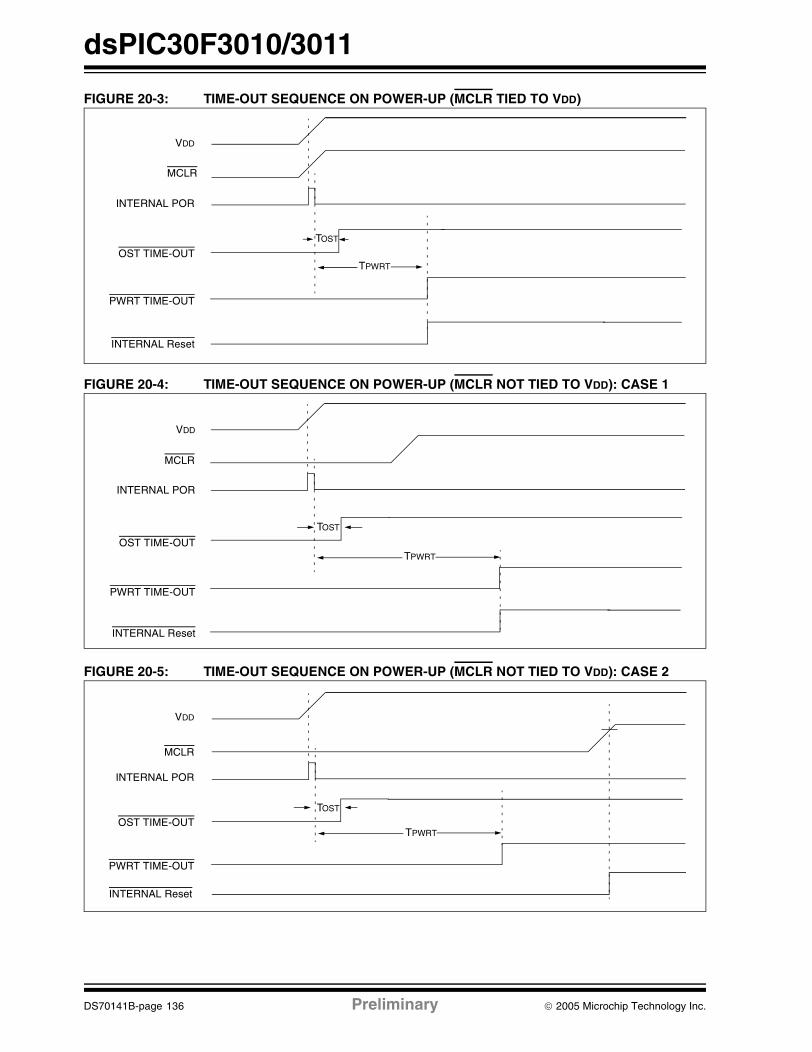
dsPIC30F3010/3011
FIGURE 20-3: TIME-OUT SEQUENCE ON POWER-UP (MCLR TIED TO VDD)
FIGURE 20-4: TIME-OUT SEQUENCE ON POWER-UP (MCLR NOT TIED TO VDD): CASE 1
FIGURE 20-5: TIME-OUT SEQUENCE ON POWER-UP (MCLR NOT TIED TO VDD): CASE 2
TPWRT
TOST
VDD
INTERNAL POR
PWRT TIME-OUT
OST TIME-OUT
INTERNAL Reset
MCLR
TPWRT
TOST
VDD
INTERNAL POR
PWRT TIME-OUT
OST TIME-OUT
INTERNAL Reset
MCLR
VDD
MCLR
INTERNAL POR
PWRT TIME-OUT
OST TIME-OUT
INTERNAL Reset
TPWRT
TOST
DS70141B-page 136 Preliminary © 2005 Microchip Technology Inc.

dsPIC30F3010/3011
20.3.1.1 POR with Long Crystal Start-up Time (with FSCM Enabled)
The oscillator start-up circuitry is not linked to the PORcircuitry. Some crystal circuits (especially low fre-quency crystals) will have a relatively long start-uptime. Therefore, one or more of the following conditionsis possible after the POR timer and the PWRT haveexpired:
• The oscillator circuit has not begun to oscillate.• The oscillator start-up timer has NOT expired (if a
crystal oscillator is used).• The PLL has not achieved a LOCK (if PLL is
used).
If the FSCM is enabled and one of the above conditionsis true, then a Clock Failure Trap will occur. The devicewill automatically switch to the FRC oscillator and theuser can switch to the desired crystal oscillator in thetrap ISR.
20.3.1.2 Operating without FSCM and PWRT
If the FSCM is disabled and the Power-up Timer(PWRT) is also disabled, then the device will exitrapidly from Reset on power-up. If the clock source isFRC, LPRC, EXTRC or EC, it will be activeimmediately.
If the FSCM is disabled and the system clock has notstarted, the device will be in a frozen state at the Resetvector until the system clock starts. From the user’sperspective, the device will appear to be in Reset untila system clock is available.
20.3.2 BOR: PROGRAMMABLE BROWN-OUT RESET
The BOR (Brown-out Reset) module is based on aninternal voltage reference circuit. The main purpose ofthe BOR module is to generate a device Reset whena brown-out condition occurs. Brown-out conditionsare generally caused by glitches on the AC mains(i.e., missing portions of the AC cycle waveform dueto bad power transmission lines or voltage sags dueto excessive current draw when a large inductive loadis turned on).
The BOR module allows selection of one of the follow-ing voltage trip points:
• 2.0V• 2.7V• 4.2V
• 4.5V
A BOR will generate a Reset pulse which will reset thedevice. The BOR will select the clock source, based onthe device configuration bit values (FOS<1:0> andFPR<3:0>). Furthermore, if an Oscillator mode isselected, the BOR will activate the Oscillator Start-upTimer (OST). The system clock is held until OSTexpires. If the PLL is used, then the clock will be helduntil the LOCK bit (OSCCON<5>) is ‘1’.
Concurrently, the POR time-out (TPOR) and the PWRTtime-out (TPWRT) will be applied before the internalReset is released. If TPWRT = 0 and a crystal oscillatoris being used, then a nominal delay of TFSCM = 100 μsis applied. The total delay in this case is (TPOR +TFSCM).
The BOR status bit (RCON<1>) will be set to indicatethat a BOR has occurred. The BOR circuit, if enabled,will continue to operate while in Sleep or Idle modesand will reset the device should VDD fall below the BORthreshold voltage.
FIGURE 20-6: EXTERNAL POWER-ON RESET CIRCUIT (FOR SLOW VDD POWER-UP)
Note: The BOR voltage trip points indicated hereare nominal values provided for designguidance only.
Note: Dedicated supervisory devices, such asthe MCP1XX and MCP8XX, may also beused as an external Power-on Resetcircuit.
Note 1: External Power-on Reset circuit isrequired only if the VDD power-up slopeis too slow. The diode D helps dischargethe capacitor quickly when VDD powersdown.
2: R should be suitably chosen so as tomake sure that the voltage drop acrossR does not violate the device’s electricalspecification.
3: R1 should be suitably chosen so as tolimit any current flowing into MCLR fromexternal capacitor C, in the event ofMCLR/VPP pin breakdown due toElectrostatic Discharge (ESD) orElectrical Overstress (EOS).
C
R1RD
VDD
dsPIC30F
MCLR
© 2005 Microchip Technology Inc. Preliminary DS70141B-page 137

dsPIC30F3010/3011
Table 20-5 shows the Reset conditions for the RCONregister. Since the control bits within the RCON registerare R/W, the information in the table implies that all thebits are negated prior to the action specified in thecondition column.
TABLE 20-5: INITIALIZATION CONDITION FOR RCON REGISTER CASE 1
Table 20-6 shows a second example of the bitconditions for the RCON register. In this case, it is notassumed the user has set/cleared specific bits prior toaction specified in the condition column.
TABLE 20-6: INITIALIZATION CONDITION FOR RCON REGISTER CASE 2
ConditionProgram Counter
TRAPR IOPUWR EXTR SWR WDTO IDLE SLEEP POR BOR
Power-on Reset 0x000000 0 0 0 0 0 0 0 1 1
Brown-out Reset 0x000000 0 0 0 0 0 0 0 0 1
MCLR Reset during normal operation
0x000000 0 0 1 0 0 0 0 0 0
Software Reset during normal operation
0x000000 0 0 0 1 0 0 0 0 0
MCLR Reset during Sleep 0x000000 0 0 1 0 0 0 1 0 0
MCLR Reset during Idle 0x000000 0 0 1 0 0 1 0 0 0
WDT Time-out Reset 0x000000 0 0 0 0 1 0 0 0 0
WDT Wake-up PC + 2 0 0 0 0 1 0 1 0 0
Interrupt Wake-up from Sleep
PC + 2(1) 0 0 0 0 0 0 1 0 0
Clock Failure Trap 0x000004 0 0 0 0 0 0 0 0 0
Trap Reset 0x000000 1 0 0 0 0 0 0 0 0
Illegal Operation Trap 0x000000 0 1 0 0 0 0 0 0 0
Legend: u = unchanged, x = unknownNote 1: When the wake-up is due to an enabled interrupt, the PC is loaded with the corresponding interrupt vector.
ConditionProgram Counter
TRAPR IOPUWR EXTR SWR WDTO IDLE SLEEP POR BOR
Power-on Reset 0x000000 0 0 0 0 0 0 0 1 1
Brown-out Reset 0x000000 u u u u u u u 0 1
MCLR Reset during normal operation
0x000000 u u 1 0 0 0 0 u u
Software Reset during normal operation
0x000000 u u 0 1 0 0 0 u u
MCLR Reset during Sleep 0x000000 u u 1 u 0 0 1 u u
MCLR Reset during Idle 0x000000 u u 1 u 0 1 0 u u
WDT Time-out Reset 0x000000 u u 0 0 1 0 0 u u
WDT Wake-up PC + 2 u u u u 1 u 1 u u
Interrupt Wake-up from Sleep
PC + 2(1) u u u u u u 1 u u
Clock Failure Trap 0x000004 u u u u u u u u u
Trap Reset 0x000000 1 u u u u u u u u
Illegal Operation Reset 0x000000 u 1 u u u u u u u
Legend: u = unchanged, x = unknownNote 1: When the wake-up is due to an enabled interrupt, the PC is loaded with the corresponding interrupt vector.
DS70141B-page 138 Preliminary © 2005 Microchip Technology Inc.

dsPIC30F3010/3011
20.4 Watchdog Timer (WDT)
20.4.1 WATCHDOG TIMER OPERATION
The primary function of the Watchdog Timer (WDT) isto reset the processor in the event of a softwaremalfunction. The WDT is a free running timer, whichruns off an on-chip RC oscillator, requiring no externalcomponent. Therefore, the WDT timer will continue tooperate even if the main processor clock (e.g., thecrystal oscillator) fails.
20.4.2 ENABLING AND DISABLING THE WDT
The Watchdog Timer can be “Enabled” or “Disabled”only through a configuration bit (FWDTEN) in theConfiguration register FWDT.
Setting FWDTEN = 1 enables the Watchdog Timer.The enabling is done when programming the device.By default, after chip-erase, FWDTEN bit = 1. Anydevice programmer capable of programmingdsPIC30F devices allows programming of this andother configuration bits.
If enabled, the WDT will increment until it overflows or“times out”. A WDT time-out will force a device Reset(except during Sleep). To prevent a WDT time-out, theuser must clear the Watchdog Timer using a CLRWDTinstruction.
If a WDT times out during Sleep, the device will wake-up. The WDTO bit in the RCON register will be clearedto indicate a wake-up resulting from a WDT time-out.
Setting FWDTEN = 0 allows user software to enable/disable the Watchdog Timer via the SWDTEN(RCON<5>) control bit.
20.5 Power-Saving Modes
There are two power-saving states that can be enteredthrough the execution of a special instruction, PWRSAV.
These are: Sleep and Idle.
The format of the PWRSAV instruction is as follows:
PWRSAV <parameter>, where ‘parameter’ definesIdle or Sleep mode.
20.5.1 SLEEP MODE
In Sleep mode, the clock to the CPU and peripherals isshutdown. If an on-chip oscillator is being used, it isshutdown.
The fail-safe clock monitor is not functional duringSleep, since there is no clock to monitor. However,LPRC clock remains active if WDT is operational duringSleep.
The Brown-out protection circuit and the Low VoltageDetect circuit, if enabled, will remain functional duringSleep.
The processor wakes up from Sleep if at least one ofthe following conditions has occurred:
• any interrupt that is individually enabled and meets the required priority level
• any Reset (POR, BOR and MCLR) • WDT time-out
On waking up from Sleep mode, the processor willrestart the same clock that was active prior to entryinto Sleep mode. When clock switching is enabled,bits COSC<1:0> will determine the oscillator sourcethat will be used on wake-up. If clock switch isdisabled, then there is only one system clock.
If the clock source is an oscillator, the clock to thedevice will be held off until OST times out (indicating astable oscillator). If PLL is used, the system clock isheld off until LOCK = 1 (indicating that the PLL isstable). In either case, TPOR, TLOCK and TPWRT delaysare applied.
If EC, FRC, LPRC or EXTRC oscillators are used, thena delay of TPOR (~ 10 μs) is applied. This is the smallestdelay possible on wake-up from Sleep.
Moreover, if LP oscillator was active during Sleep, andLP is the oscillator used on wake-up, then the start-updelay will be equal to TPOR. PWRT delay and OSTtimer delay are not applied. In order to have the small-est possible start-up delay when waking up from Sleep,one of these faster wake-up options should be selectedbefore entering Sleep.
Note: If a POR or BOR occurred, the selection ofthe oscillator is based on the FOS<1:0>and FPR<3:0> configuration bits.
© 2005 Microchip Technology Inc. Preliminary DS70141B-page 139

dsPIC30F3010/3011
Any interrupt that is individually enabled (using thecorresponding IE bit) and meets the prevailing prioritylevel will be able to wake-up the processor. The proces-sor will process the interrupt and branch to the ISR.The Sleep status bit in RCON register is set uponwake-up.
All Resets will wake-up the processor from Sleepmode. Any Reset, other than POR, will set the Sleepstatus bit. In a POR, the Sleep bit is cleared.
If Watchdog Timer is enabled, then the processor willwake-up from Sleep mode upon WDT time-out. TheSleep and WDTO status bits are both set.
20.5.2 IDLE MODE
In Idle mode, the clock to the CPU is shutdown whileperipherals keep running. Unlike Sleep mode, the clocksource remains active.
Several peripherals have a control bit in each module,that allows them to operate during Idle.
LPRC fail-safe clock remains active if clock failuredetect is enabled.
The processor wakes up from Idle if at least one of thefollowing conditions is true:
• on any interrupt that is individually enabled (IE bit is ‘1’) and meets the required priority level
• on any Reset (POR, BOR, MCLR)• on WDT time-out
Upon wake-up from Idle mode, the clock is re-appliedto the CPU and instruction execution beginsimmediately, starting with the instruction following thePWRSAV instruction.
Any interrupt that is individually enabled (using IE bit)and meets the prevailing priority level will be able towake-up the processor. The processor will process theinterrupt and branch to the ISR. The Idle status bit inRCON register is set upon wake-up.
Any Reset, other than POR, will set the Idle status bit.On a POR, the Idle bit is cleared.
If Watchdog Timer is enabled, then the processor willwake-up from Idle mode upon WDT time-out. The Idleand WDTO status bits are both set.
Unlike wake-up from Sleep, there are no time delaysinvolved in wake-up from Idle.
20.6 Device Configuration Registers
The configuration bits in each device configurationregister specify some of the device modes and are pro-grammed by a device programmer, or by using theIn-Circuit Serial Programming (ICSP) feature of thedevice. Each device configuration register is a 24-bitregister, but only the lower 16 bits of each register areused to hold configuration data. There are four deviceconfiguration registers available to the user:
1. FOSc (0xF80000): Oscillator Configuration register
2. FWDT (0xF80002): Watchdog Timer Configuration register
3. FBORPOR (0xF80004): BOR and POR Configuration register
4. FGS (0xF8000A): General Code Segment Configuration register
The placement of the configuration bits is automaticallyhandled when you select the device in your deviceprogrammer. The desired state of the configuration bitsmay be specified in the source code (dependent on thelanguage tool used), or through the programminginterface. After the device has been programmed, theapplication software may read the configuration bitvalues through the table read instructions. Foradditional information, please refer to the programmingspecifications of the device.
Note: In spite of various delays applied (TPOR,TLOCK and TPWRT), the crystal oscillator(and PLL) may not be active at the end ofthe time-out (e.g., for low frequency crys-tals. In such cases), if FSCM is enabled,then the device will detect this as a clockfailure and process the Clock Failure Trap,the FRC oscillator will be enabled, and theuser will have to re-enable the crystaloscillator. If FSCM is not enabled, then thedevice will simply suspend execution ofcode until the clock is stable, and willremain in Sleep until the oscillator clockhas started.
Note: If the code protection configuration fusebits (FGS<GCP> and FGS<GWRP>)have been programmed, an erase of theentire code-protected device is onlypossible at voltages VDD ≥ 4.5V.
DS70141B-page 140 Preliminary © 2005 Microchip Technology Inc.

dsPIC30F3010/3011
20.7 In-Circuit Debugger
When MPLAB ICD 2 is selected as a debugger, thein-circuit debugging functionality is enabled. This func-tion allows simple debugging functions when used withMPLAB IDE. When the device has this feature enabled,some of the resources are not available for generaluse. These resources include the first 80 bytes of dataRAM and two I/O pins.
One of four pairs of debug I/O pins may be selected bythe user using configuration options in MPLAB IDE.These pin pairs are named EMUD/EMUC, EMUD1/EMUC1, EMUD2/EMUC2 and EMUD3/EMUC3.
In each case, the selected EMUD pin is the Emulation/Debug Data line, and the EMUC pin is the Emulation/Debug Clock line. These pins will interface to theMPLAB ICD 2 module available from Microchip. Theselected pair of debug I/O pins is used by MPLABICD 2 to send commands and receive responses, aswell as to send and receive data. To use the In-CircuitDebugger function of the device, the design mustimplement ICSP connections to MCLR, VDD, VSS,PGC, PGD and the selected EMUDx/EMUCx pin pair.
This gives rise to two possibilities:
1. If EMUD/EMUC is selected as the debug I/O pinpair, then only a 5-pin interface is required, asthe EMUD and EMUC pin functions are multi-plexed with the PGD and PGC pin functions inall dsPIC30F devices.
2. If EMUD1/EMUC1, EMUD2/EMUC2 or EMUD3/EMUC3 is selected as the debug I/O pin pair,then a 7-pin interface is required, as theEMUDx/EMUCx pin functions (x = 1, 2 or 3) arenot multiplexed with the PGD and PGC pinfunctions.
© 2005 Microchip Technology Inc. Preliminary DS70141B-page 141

dsPIC30F3010/3011
TABL
E 2
0-7:
SY
ST
EM
INT
EG
RA
TIO
N R
EG
IST
ER
MA
P
TAB
LE
20-
8:D
EV
ICE
CO
NF
IGU
RA
TIO
N R
EG
IST
ER
MA
P
SF
R
Nam
eA
dd
r.
Bit
15
Bit
14
Bit
13
Bit
12
Bit
11
Bit
10
Bit
9B
it 8
Bit
7B
it 6
Bit
5B
it 4
Bit
3B
it 2
Bit
1B
it 0
Res
et S
tate
RC
ON
0740
TR
AP
RIO
PU
WR
BG
ST
—E
XT
RS
WR
SW
DT
EN
WD
TO
SLE
EP
IDLE
BO
RP
OR
Dep
ends
on
type
of R
eset
.
OS
CC
ON
0742
TU
N3
TU
N2
CO
SC
<1:
0>T
UN
1T
UN
0N
OS
C<
1:0>
PO
ST
<1:
0>LO
CK
—C
F—
LPO
SC
EN
OS
WE
ND
epen
ds o
n co
nfig
urat
ion
bits
.
Leg
end
:u
= u
nini
tializ
ed b
it; —
= u
nim
plem
ente
d bi
t
No
te1:
Ref
er to
dsP
IC30
F F
amily
Ref
eren
ce M
anua
l (D
S70
046)
for
desc
riptio
ns o
f reg
iste
r bi
t fie
lds.
Not
all
perip
hera
ls, a
nd th
eref
ore
thei
r bi
t pos
ition
s, a
re a
vaila
ble
on th
is d
evic
e.
File
Nam
eA
dd
r.B
its 2
3-16
Bit
15
Bit
14
Bit
13
Bit
12
Bit
11
Bit
10
Bit
9B
it 8
Bit
7B
it 6
Bit
5B
it 4
Bit
3B
it 2
Bit
1B
it 0
FO
SC
F80
000
—F
CK
SM
<1:
0>—
——
—F
OS
<1:
0>—
——
—F
PR
<3:
0>
FW
DT
F80
002
—F
WD
TE
N—
——
——
——
——
FW
PS
A<
1:0>
FW
PS
B<
3:0>
FB
OR
PO
RF
8000
4—
MC
LRE
N—
——
—P
WM
PIN
HP
OL
LPO
LB
OR
EN
—B
OR
V<
1:0>
——
FP
WR
T<
1:0>
FG
SF
8000
A—
——
——
——
——
——
——
——
GC
PG
WR
P
Leg
end
:u
= u
nini
tializ
ed b
it; —
= u
nim
plem
ente
d bi
t
No
te1:
Ref
er to
dsP
IC30
F F
amily
Ref
eren
ce M
anua
l (D
S70
046)
for
desc
riptio
ns o
f reg
iste
r bi
t fie
lds.
Not
all
perip
hera
ls, a
nd th
eref
ore
thei
r bi
t pos
ition
s, a
re a
vaila
ble
on th
is d
evic
e.
DS70141B-page 142 Preliminary © 2005 Microchip Technology Inc.

dsPIC30F3010/3011
21.0 INSTRUCTION SET SUMMARY
The dsPIC30F instruction set adds manyenhancements to the previous PICmicro®
microcontroller (MCU) instruction sets, whilemaintaining an easy migration from PICmicro MCUinstruction sets.
Most instructions are a single program memory word(24-bits). Only three instructions require two programmemory locations.
Each single-word instruction is a 24-bit word dividedinto an 8-bit opcode which specifies the instructiontype, and one or more operands which further specifythe operation of the instruction.
The instruction set is highly orthogonal and is groupedinto five basic categories:
• Word or byte-oriented operations
• Bit-oriented operations• Literal operations• DSP operations
• Control operations
Table 21-1 shows the general symbols used indescribing the instructions.
The dsPIC30F instruction set summary in Table 21-2lists all the instructions along with the status flagsaffected by each instruction.
Most word or byte-oriented W register instructions(including barrel shift instructions) have threeoperands:
• The first source operand, which is typically a register ‘Wb’ without any address modifier
• The second source operand, which is typically a register ‘Ws’ with or without an address modifier
• The destination of the result, which is typically a register ‘Wd’ with or without an address modifier
However, word or byte-oriented file register instructionshave two operands:
• The File register specified by the value ‘f’
• The destination, which could either be the File register ‘f’ or the W0 register, which is denoted as ‘WREG’
Most bit oriented instructions (including simple rotate/shift instructions) have two operands:
• The W register (with or without an address modi-fier) or File register (specified by the value of ‘Ws’ or ‘f’)
• The bit in the W register or File register (specified by a literal value, or indirectly by the contents of register ‘Wb’)
The literal instructions that involve data movement mayuse some of the following operands:
• A literal value to be loaded into a W register or File register (specified by the value of ‘k’)
• The W register or File register where the literal value is to be loaded (specified by ‘Wb’ or ‘f’)
However, literal instructions that involve arithmetic orlogical operations use some of the following operands:
• The first source operand, which is a register ‘Wb’ without any address modifier
• The second source operand, which is a literal value
• The destination of the result (only if not the same as the first source operand), which is typically a register ‘Wd’ with or without an address modifier
The MAC class of DSP instructions may use some of thefollowing operands:
• The accumulator (A or B) to be used (required operand)
• The W registers to be used as the two operands• The X and Y address space pre-fetch operations• The X and Y address space pre-fetch destinations
• The accumulator write back destination
The other DSP instructions do not involve anymultiplication, and may include:
• The accumulator to be used (required)
• The source or destination operand (designated as Wso or Wdo, respectively) with or without an address modifier
• The amount of shift, specified by a W register ‘Wn’ or a literal value
The control instructions may use some of the followingoperands:
• A program memory address • The mode of the Table Read and Table Write
instructions
All instructions are a single word, except for certaindouble-word instructions, which were made double-word instructions so that all the required information isavailable in these 48-bits. In the second word, the8 MSb’s are 0’s. If this second word is executed as aninstruction (by itself), it will execute as a NOP.
Note: This data sheet summarizes features of this groupof dsPIC30F devices and is not intended to be a completereference source. For more information on the CPU,peripherals, register descriptions and general devicefunctionality, refer to the dsPIC30F Family ReferenceManual (DS70046). For more information on the deviceinstruction set and programming, refer to the dsPIC30FProgrammer’s Reference Manual (DS70030).
© 2005 Microchip Technology Inc. Preliminary DS70141B-page 143

dsPIC30F3010/3011
Most single word instructions are executed in a singleinstruction cycle, unless a conditional test is true or theprogram counter is changed as a result of the instruc-tion. In these cases, the execution takes two instructioncycles with the additional instruction cycle(s) executedas a NOP. Notable exceptions are the BRA (uncondi-tional/computed branch), indirect CALL/GOTO, allTable Reads and Writes and RETURN/RETFIE instruc-tions, which are single word instructions, but take twoor three cycles. Certain instructions that involve skip-ping over the subsequent instruction, require either two
or three cycles if the skip is performed, depending onwhether the instruction being skipped is a single-wordor two-word instruction. Moreover, double-word movesrequire two cycles. The double-word instructionsexecute in two instruction cycles.
Note: For more details on the instruction set,refer to the dsPIC30F Programmer’sReference Manual (DS70030).
TABLE 21-1: SYMBOLS USED IN OPCODE DESCRIPTIONS
Field Description
#text Means literal defined by “text“(text) Means “content of text“[text] Means “the location addressed by text”
{ } Optional field or operation<n:m> Register bit field.b Byte mode selection
.d Double-word mode selection
.S Shadow register select
.w Word mode selection (default)
Acc One of two accumulators {A, B}AWB Accumulator Write Back Destination Address register ∈ {W13, [W13]+=2}bit4 4-bit bit selection field (used in word addressed instructions) ∈ {0...15}
C, DC, N, OV, Z MCU status bits: Carry, Digit Carry, Negative, Overflow, ZeroExpr Absolute address, label or expression (resolved by the linker)f File register address ∈ {0x0000...0x1FFF}
lit1 1-bit unsigned literal ∈ {0,1}lit4 4-bit unsigned literal ∈ {0...15}lit5 5-bit unsigned literal ∈ {0...31}
lit8 8-bit unsigned literal ∈ {0...255}lit10 10-bit unsigned literal ∈ {0...255} for Byte mode, {0:1023} for Word modelit14 14-bit unsigned literal ∈ {0...16384}
lit16 16-bit unsigned literal ∈ {0...65535}lit23 23-bit unsigned literal ∈ {0...8388608}; LSB must be 0None Field does not require an entry, may be blank
OA, OB, SA, SB DSP status bits: AccA Overflow, AccB Overflow, AccA Saturate, AccB SaturatePC Program CounterSlit10 10-bit signed literal ∈ {-512...511}
Slit16 16-bit signed literal ∈ {-32768...32767}Slit6 6-bit signed literal ∈ {-16...16}
DS70141B-page 144 Preliminary © 2005 Microchip Technology Inc.

dsPIC30F3010/3011
Wb Base W register ∈ {W0..W15}
Wd Destination W register ∈ { Wd, [Wd], [Wd++], [Wd--], [++Wd], [--Wd] }Wdo Destination W register ∈
{ Wnd, [Wnd], [Wnd++], [Wnd--], [++Wnd], [--Wnd], [Wnd+Wb] } Wm,Wn Dividend, Divisor working register pair (direct addressing)Wm*Wm Multiplicand and Multiplier working register pair for Square instructions ∈
{W4*W4,W5*W5,W6*W6,W7*W7} Wm*Wn Multiplicand and Multiplier working register pair for DSP instructions ∈
{W4*W5,W4*W6,W4*W7,W5*W6,W5*W7,W6*W7}Wn One of 16 working registers ∈ {W0..W15}
Wnd One of 16 destination working registers ∈ {W0..W15}Wns One of 16 source working registers ∈ {W0..W15}WREG W0 (working register used in File register instructions)
Ws Source W register ∈ { Ws, [Ws], [Ws++], [Ws--], [++Ws], [--Ws] }Wso Source W register ∈
{ Wns, [Wns], [Wns++], [Wns--], [++Wns], [--Wns], [Wns+Wb] } Wx X data space Pre-fetch Address register for DSP instructions
∈ {[W8]+=6, [W8]+=4, [W8]+=2, [W8], [W8]-=6, [W8]-=4, [W8]-=2, [W9]+=6, [W9]+=4, [W9]+=2, [W9], [W9]-=6, [W9]-=4, [W9]-=2, [W9+W12],none}
Wxd X data space Pre-fetch Destination register for DSP instructions ∈ {W4..W7}
Wy Y data space Pre-fetch Address register for DSP instructions ∈ {[W10]+=6, [W10]+=4, [W10]+=2, [W10], [W10]-=6, [W10]-=4, [W10]-=2, [W11]+=6, [W11]+=4, [W11]+=2, [W11], [W11]-=6, [W11]-=4, [W11]-=2, [W11+W12], none}
Wyd Y data space Pre-fetch Destination register for DSP instructions ∈ {W4..W7}
TABLE 21-1: SYMBOLS USED IN OPCODE DESCRIPTIONS (CONTINUED)
Field Description
© 2005 Microchip Technology Inc. Preliminary DS70141B-page 145
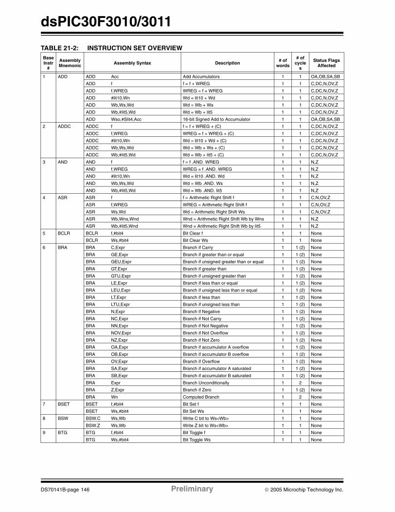
dsPIC30F3010/3011
TABLE 21-2: INSTRUCTION SET OVERVIEW BaseInstr
#
AssemblyMnemonic Assembly Syntax Description # of
words
# of cycle
s
Status Flags Affected
1 ADD ADD Acc Add Accumulators 1 1 OA,OB,SA,SB
ADD f f = f + WREG 1 1 C,DC,N,OV,Z
ADD f,WREG WREG = f + WREG 1 1 C,DC,N,OV,Z
ADD #lit10,Wn Wd = lit10 + Wd 1 1 C,DC,N,OV,Z
ADD Wb,Ws,Wd Wd = Wb + Ws 1 1 C,DC,N,OV,Z
ADD Wb,#lit5,Wd Wd = Wb + lit5 1 1 C,DC,N,OV,Z
ADD Wso,#Slit4,Acc 16-bit Signed Add to Accumulator 1 1 OA,OB,SA,SB
2 ADDC ADDC f f = f + WREG + (C) 1 1 C,DC,N,OV,Z
ADDC f,WREG WREG = f + WREG + (C) 1 1 C,DC,N,OV,Z
ADDC #lit10,Wn Wd = lit10 + Wd + (C) 1 1 C,DC,N,OV,Z
ADDC Wb,Ws,Wd Wd = Wb + Ws + (C) 1 1 C,DC,N,OV,Z
ADDC Wb,#lit5,Wd Wd = Wb + lit5 + (C) 1 1 C,DC,N,OV,Z
3 AND AND f f = f .AND. WREG 1 1 N,Z
AND f,WREG WREG = f .AND. WREG 1 1 N,Z
AND #lit10,Wn Wd = lit10 .AND. Wd 1 1 N,Z
AND Wb,Ws,Wd Wd = Wb .AND. Ws 1 1 N,Z
AND Wb,#lit5,Wd Wd = Wb .AND. lit5 1 1 N,Z
4 ASR ASR f f = Arithmetic Right Shift f 1 1 C,N,OV,Z
ASR f,WREG WREG = Arithmetic Right Shift f 1 1 C,N,OV,Z
ASR Ws,Wd Wd = Arithmetic Right Shift Ws 1 1 C,N,OV,Z
ASR Wb,Wns,Wnd Wnd = Arithmetic Right Shift Wb by Wns 1 1 N,Z
ASR Wb,#lit5,Wnd Wnd = Arithmetic Right Shift Wb by lit5 1 1 N,Z
5 BCLR BCLR f,#bit4 Bit Clear f 1 1 None
BCLR Ws,#bit4 Bit Clear Ws 1 1 None
6 BRA BRA C,Expr Branch if Carry 1 1 (2) None
BRA GE,Expr Branch if greater than or equal 1 1 (2) None
BRA GEU,Expr Branch if unsigned greater than or equal 1 1 (2) None
BRA GT,Expr Branch if greater than 1 1 (2) None
BRA GTU,Expr Branch if unsigned greater than 1 1 (2) None
BRA LE,Expr Branch if less than or equal 1 1 (2) None
BRA LEU,Expr Branch if unsigned less than or equal 1 1 (2) None
BRA LT,Expr Branch if less than 1 1 (2) None
BRA LTU,Expr Branch if unsigned less than 1 1 (2) None
BRA N,Expr Branch if Negative 1 1 (2) None
BRA NC,Expr Branch if Not Carry 1 1 (2) None
BRA NN,Expr Branch if Not Negative 1 1 (2) None
BRA NOV,Expr Branch if Not Overflow 1 1 (2) None
BRA NZ,Expr Branch if Not Zero 1 1 (2) None
BRA OA,Expr Branch if accumulator A overflow 1 1 (2) None
BRA OB,Expr Branch if accumulator B overflow 1 1 (2) None
BRA OV,Expr Branch if Overflow 1 1 (2) None
BRA SA,Expr Branch if accumulator A saturated 1 1 (2) None
BRA SB,Expr Branch if accumulator B saturated 1 1 (2) None
BRA Expr Branch Unconditionally 1 2 None
BRA Z,Expr Branch if Zero 1 1 (2) None
BRA Wn Computed Branch 1 2 None
7 BSET BSET f,#bit4 Bit Set f 1 1 None
BSET Ws,#bit4 Bit Set Ws 1 1 None
8 BSW BSW.C Ws,Wb Write C bit to Ws<Wb> 1 1 None
BSW.Z Ws,Wb Write Z bit to Ws<Wb> 1 1 None
9 BTG BTG f,#bit4 Bit Toggle f 1 1 None
BTG Ws,#bit4 Bit Toggle Ws 1 1 None
DS70141B-page 146 Preliminary © 2005 Microchip Technology Inc.
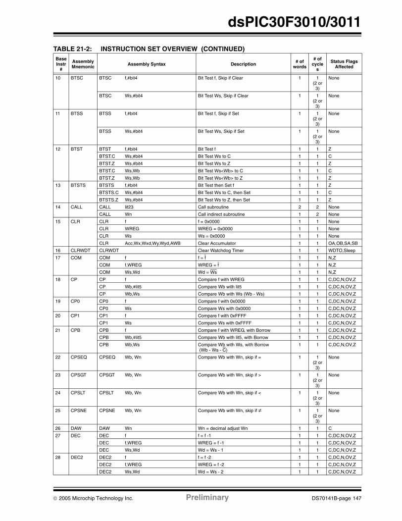
dsPIC30F3010/3011
10 BTSC BTSC f,#bit4 Bit Test f, Skip if Clear 1 1 (2 or
3)
None
BTSC Ws,#bit4 Bit Test Ws, Skip if Clear 1 1 (2 or
3)
None
11 BTSS BTSS f,#bit4 Bit Test f, Skip if Set 1 1 (2 or
3)
None
BTSS Ws,#bit4 Bit Test Ws, Skip if Set 1 1 (2 or
3)
None
12 BTST BTST f,#bit4 Bit Test f 1 1 Z
BTST.C Ws,#bit4 Bit Test Ws to C 1 1 C
BTST.Z Ws,#bit4 Bit Test Ws to Z 1 1 Z
BTST.C Ws,Wb Bit Test Ws<Wb> to C 1 1 C
BTST.Z Ws,Wb Bit Test Ws<Wb> to Z 1 1 Z
13 BTSTS BTSTS f,#bit4 Bit Test then Set f 1 1 Z
BTSTS.C Ws,#bit4 Bit Test Ws to C, then Set 1 1 C
BTSTS.Z Ws,#bit4 Bit Test Ws to Z, then Set 1 1 Z
14 CALL CALL lit23 Call subroutine 2 2 None
CALL Wn Call indirect subroutine 1 2 None
15 CLR CLR f f = 0x0000 1 1 None
CLR WREG WREG = 0x0000 1 1 None
CLR Ws Ws = 0x0000 1 1 None
CLR Acc,Wx,Wxd,Wy,Wyd,AWB Clear Accumulator 1 1 OA,OB,SA,SB
16 CLRWDT CLRWDT Clear Watchdog Timer 1 1 WDTO,Sleep
17 COM COM f f = f 1 1 N,Z
COM f,WREG WREG = f 1 1 N,Z
COM Ws,Wd Wd = Ws 1 1 N,Z
18 CP CP f Compare f with WREG 1 1 C,DC,N,OV,Z
CP Wb,#lit5 Compare Wb with lit5 1 1 C,DC,N,OV,Z
CP Wb,Ws Compare Wb with Ws (Wb - Ws) 1 1 C,DC,N,OV,Z
19 CP0 CP0 f Compare f with 0x0000 1 1 C,DC,N,OV,Z
CP0 Ws Compare Ws with 0x0000 1 1 C,DC,N,OV,Z
20 CP1 CP1 f Compare f with 0xFFFF 1 1 C,DC,N,OV,Z
CP1 Ws Compare Ws with 0xFFFF 1 1 C,DC,N,OV,Z
21 CPB CPB f Compare f with WREG, with Borrow 1 1 C,DC,N,OV,Z
CPB Wb,#lit5 Compare Wb with lit5, with Borrow 1 1 C,DC,N,OV,Z
CPB Wb,Ws Compare Wb with Ws, with Borrow (Wb - Ws - C)
1 1 C,DC,N,OV,Z
22 CPSEQ CPSEQ Wb, Wn Compare Wb with Wn, skip if = 1 1 (2 or
3)
None
23 CPSGT CPSGT Wb, Wn Compare Wb with Wn, skip if > 1 1 (2 or
3)
None
24 CPSLT CPSLT Wb, Wn Compare Wb with Wn, skip if < 1 1 (2 or
3)
None
25 CPSNE CPSNE Wb, Wn Compare Wb with Wn, skip if ≠ 1 1 (2 or
3)
None
26 DAW DAW Wn Wn = decimal adjust Wn 1 1 C
27 DEC DEC f f = f -1 1 1 C,DC,N,OV,Z
DEC f,WREG WREG = f -1 1 1 C,DC,N,OV,Z
DEC Ws,Wd Wd = Ws - 1 1 1 C,DC,N,OV,Z
28 DEC2 DEC2 f f = f -2 1 1 C,DC,N,OV,Z
DEC2 f,WREG WREG = f -2 1 1 C,DC,N,OV,Z
DEC2 Ws,Wd Wd = Ws - 2 1 1 C,DC,N,OV,Z
TABLE 21-2: INSTRUCTION SET OVERVIEW (CONTINUED)BaseInstr
#
AssemblyMnemonic Assembly Syntax Description # of
words
# of cycle
s
Status Flags Affected
© 2005 Microchip Technology Inc. Preliminary DS70141B-page 147

dsPIC30F3010/3011
29 DISI DISI #lit14 Disable Interrupts for k instruction cycles 1 1 None
30 DIV DIV.S Wm,Wn Signed 16/16-bit Integer Divide 1 18 N,Z,C, OV
DIV.SD Wm,Wn Signed 32/16-bit Integer Divide 1 18 N,Z,C, OV
DIV.U Wm,Wn Unsigned 16/16-bit Integer Divide 1 18 N,Z,C, OV
DIV.UD Wm,Wn Unsigned 32/16-bit Integer Divide 1 18 N,Z,C, OV
31 DIVF DIVF Wm,Wn Signed 16/16-bit Fractional Divide 1 18 N,Z,C, OV
32 DO DO #lit14,Expr Do code to PC+Expr, lit14+1 times 2 2 None
DO Wn,Expr Do code to PC+Expr, (Wn)+1 times 2 2 None
33 ED ED Wm*Wm,Acc,Wx,Wy,Wxd Euclidean Distance ( no accumulate) 1 1 OA,OB,OAB,SA,SB,SAB
34 EDAC EDAC Wm*Wm,Acc,Wx,Wy,Wxd Euclidean Distance 1 1 OA,OB,OAB,SA,SB,SAB
35 EXCH EXCH Wns,Wnd Swap Wns with Wnd 1 1 None
36 FBCL FBCL Ws,Wnd Find Bit Change from Left (MSb) Side 1 1 C
37 FF1L FF1L Ws,Wnd Find First One from Left (MSb) Side 1 1 C
38 FF1R FF1R Ws,Wnd Find First One from Right (LSb) Side 1 1 C
39 GOTO GOTO Expr Go to address 2 2 None
GOTO Wn Go to indirect 1 2 None
40 INC INC f f = f + 1 1 1 C,DC,N,OV,Z
INC f,WREG WREG = f + 1 1 1 C,DC,N,OV,Z
INC Ws,Wd Wd = Ws + 1 1 1 C,DC,N,OV,Z
41 INC2 INC2 f f = f + 2 1 1 C,DC,N,OV,Z
INC2 f,WREG WREG = f + 2 1 1 C,DC,N,OV,Z
INC2 Ws,Wd Wd = Ws + 2 1 1 C,DC,N,OV,Z
42 IOR IOR f f = f .IOR. WREG 1 1 N,Z
IOR f,WREG WREG = f .IOR. WREG 1 1 N,Z
IOR #lit10,Wn Wd = lit10 .IOR. Wd 1 1 N,Z
IOR Wb,Ws,Wd Wd = Wb .IOR. Ws 1 1 N,Z
IOR Wb,#lit5,Wd Wd = Wb .IOR. lit5 1 1 N,Z
43 LAC LAC Wso,#Slit4,Acc Load Accumulator 1 1 OA,OB,OAB,SA,SB,SAB
44 LNK LNK #lit14 Link frame pointer 1 1 None
45 LSR LSR f f = Logical Right Shift f 1 1 C,N,OV,Z
LSR f,WREG WREG = Logical Right Shift f 1 1 C,N,OV,Z
LSR Ws,Wd Wd = Logical Right Shift Ws 1 1 C,N,OV,Z
LSR Wb,Wns,Wnd Wnd = Logical Right Shift Wb by Wns 1 1 N,Z
LSR Wb,#lit5,Wnd Wnd = Logical Right Shift Wb by lit5 1 1 N,Z
46 MAC MAC Wm*Wn,Acc,Wx,Wxd,Wy,Wyd,AWB
Multiply and Accumulate 1 1 OA,OB,OAB,SA,SB,SAB
MAC Wm*Wm,Acc,Wx,Wxd,Wy,Wyd Square and Accumulate 1 1 OA,OB,OAB,SA,SB,SAB
47 MOV MOV f,Wn Move f to Wn 1 1 None
MOV f Move f to f 1 1 N,Z
MOV f,WREG Move f to WREG 1 1 N,Z
MOV #lit16,Wn Move 16-bit literal to Wn 1 1 None
MOV.b #lit8,Wn Move 8-bit literal to Wn 1 1 None
MOV Wn,f Move Wn to f 1 1 None
MOV Wso,Wdo Move Ws to Wd 1 1 None
MOV WREG,f Move WREG to f 1 1 N,Z
MOV.D Wns,Wd Move Double from W(ns):W(ns+1) to Wd 1 2 None
MOV.D Ws,Wnd Move Double from Ws to W(nd+1):W(nd) 1 2 None
48 MOVSAC MOVSAC Acc,Wx,Wxd,Wy,Wyd,AWB Pre-fetch and store accumulator 1 1 None
49 MPY MPY Wm*Wn,Acc,Wx,Wxd,Wy,Wyd Multiply Wm by Wn to Accumulator 1 1 OA,OB,OAB,SA,SB,SAB
MPY Wm*Wm,Acc,Wx,Wxd,Wy,Wyd Square Wm to Accumulator 1 1 OA,OB,OAB,SA,SB,SAB
50 MPY.N MPY.N Wm*Wn,Acc,Wx,Wxd,Wy,Wyd -(Multiply Wm by Wn) to Accumulator 1 1 None
TABLE 21-2: INSTRUCTION SET OVERVIEW (CONTINUED)BaseInstr
#
AssemblyMnemonic Assembly Syntax Description # of
words
# of cycle
s
Status Flags Affected
DS70141B-page 148 Preliminary © 2005 Microchip Technology Inc.

dsPIC30F3010/3011
51 MSC MSC Wm*Wm,Acc,Wx,Wxd,Wy,Wyd,AWB
Multiply and Subtract from Accumulator 1 1 OA,OB,OAB,SA,SB,SAB
52 MUL MUL.SS Wb,Ws,Wnd {Wnd+1, Wnd} = signed(Wb) * signed(Ws) 1 1 None
MUL.SU Wb,Ws,Wnd {Wnd+1, Wnd} = signed(Wb) * unsigned(Ws) 1 1 None
MUL.US Wb,Ws,Wnd {Wnd+1, Wnd} = unsigned(Wb) * signed(Ws) 1 1 None
MUL.UU Wb,Ws,Wnd {Wnd+1, Wnd} = unsigned(Wb) * unsigned(Ws)
1 1 None
MUL.SU Wb,#lit5,Wnd {Wnd+1, Wnd} = signed(Wb) * unsigned(lit5) 1 1 None
MUL.UU Wb,#lit5,Wnd {Wnd+1, Wnd} = unsigned(Wb) * unsigned(lit5)
1 1 None
MUL f W3:W2 = f * WREG 1 1 None
53 NEG NEG Acc Negate Accumulator 1 1 OA,OB,OAB,SA,SB,SAB
NEG f f = f + 1 1 1 C,DC,N,OV,Z
NEG f,WREG WREG = f + 1 1 1 C,DC,N,OV,Z
NEG Ws,Wd Wd = Ws + 1 1 1 C,DC,N,OV,Z
54 NOP NOP No Operation 1 1 None
NOPR No Operation 1 1 None
55 POP POP f Pop f from top-of-stack (TOS) 1 1 None
POP Wdo Pop from top-of-stack (TOS) to Wdo 1 1 None
POP.D Wnd Pop from top-of-stack (TOS) to W(nd):W(nd+1)
1 2 None
POP.S Pop Shadow Registers 1 1 All
56 PUSH PUSH f Push f to top-of-stack (TOS) 1 1 None
PUSH Wso Push Wso to top-of-stack (TOS) 1 1 None
PUSH.D Wns Push W(ns):W(ns+1) to top-of-stack (TOS) 1 2 None
PUSH.S Push Shadow Registers 1 1 None
57 PWRSAV PWRSAV #lit1 Go into Sleep or Idle mode 1 1 WDTO,Sleep
58 RCALL RCALL Expr Relative Call 1 2 None
RCALL Wn Computed Call 1 2 None
59 REPEAT REPEAT #lit14 Repeat Next Instruction lit14+1 times 1 1 None
REPEAT Wn Repeat Next Instruction (Wn)+1 times 1 1 None
60 RESET RESET Software device Reset 1 1 None
61 RETFIE RETFIE Return from interrupt 1 3 (2) None
62 RETLW RETLW #lit10,Wn Return with literal in Wn 1 3 (2) None
63 RETURN RETURN Return from Subroutine 1 3 (2) None
64 RLC RLC f f = Rotate Left through Carry f 1 1 C,N,Z
RLC f,WREG WREG = Rotate Left through Carry f 1 1 C,N,Z
RLC Ws,Wd Wd = Rotate Left through Carry Ws 1 1 C,N,Z
65 RLNC RLNC f f = Rotate Left (No Carry) f 1 1 N,Z
RLNC f,WREG WREG = Rotate Left (No Carry) f 1 1 N,Z
RLNC Ws,Wd Wd = Rotate Left (No Carry) Ws 1 1 N,Z
66 RRC RRC f f = Rotate Right through Carry f 1 1 C,N,Z
RRC f,WREG WREG = Rotate Right through Carry f 1 1 C,N,Z
RRC Ws,Wd Wd = Rotate Right through Carry Ws 1 1 C,N,Z
67 RRNC RRNC f f = Rotate Right (No Carry) f 1 1 N,Z
RRNC f,WREG WREG = Rotate Right (No Carry) f 1 1 N,Z
RRNC Ws,Wd Wd = Rotate Right (No Carry) Ws 1 1 N,Z
68 SAC SAC Acc,#Slit4,Wdo Store Accumulator 1 1 None
SAC.R Acc,#Slit4,Wdo Store Rounded Accumulator 1 1 None
69 SE SE Ws,Wnd Wnd = sign extended Ws 1 1 C,N,Z
70 SETM SETM f f = 0xFFFF 1 1 None
SETM WREG WREG = 0xFFFF 1 1 None
SETM Ws Ws = 0xFFFF 1 1 None
TABLE 21-2: INSTRUCTION SET OVERVIEW (CONTINUED)BaseInstr
#
AssemblyMnemonic Assembly Syntax Description # of
words
# of cycle
s
Status Flags Affected
© 2005 Microchip Technology Inc. Preliminary DS70141B-page 149

dsPIC30F3010/3011
71 SFTAC SFTAC Acc,Wn Arithmetic Shift Accumulator by (Wn) 1 1 OA,OB,OAB,SA,SB,SAB
SFTAC Acc,#Slit6 Arithmetic Shift Accumulator by Slit6 1 1 OA,OB,OAB,SA,SB,SAB
72 SL SL f f = Left Shift f 1 1 C,N,OV,Z
SL f,WREG WREG = Left Shift f 1 1 C,N,OV,Z
SL Ws,Wd Wd = Left Shift Ws 1 1 C,N,OV,Z
SL Wb,Wns,Wnd Wnd = Left Shift Wb by Wns 1 1 N,Z
SL Wb,#lit5,Wnd Wnd = Left Shift Wb by lit5 1 1 N,Z
73 SUB SUB Acc Subtract Accumulators 1 1 OA,OB,OAB,SA,SB,SAB
SUB f f = f - WREG 1 1 C,DC,N,OV,Z
SUB f,WREG WREG = f - WREG 1 1 C,DC,N,OV,Z
SUB #lit10,Wn Wn = Wn - lit10 1 1 C,DC,N,OV,Z
SUB Wb,Ws,Wd Wd = Wb - Ws 1 1 C,DC,N,OV,Z
SUB Wb,#lit5,Wd Wd = Wb - lit5 1 1 C,DC,N,OV,Z
74 SUBB SUBB f f = f - WREG - (C) 1 1 C,DC,N,OV,Z
SUBB f,WREG WREG = f - WREG - (C) 1 1 C,DC,N,OV,Z
SUBB #lit10,Wn Wn = Wn - lit10 - (C) 1 1 C,DC,N,OV,Z
SUBB Wb,Ws,Wd Wd = Wb - Ws - (C) 1 1 C,DC,N,OV,Z
SUBB Wb,#lit5,Wd Wd = Wb - lit5 - (C) 1 1 C,DC,N,OV,Z
75 SUBR SUBR f f = WREG - f 1 1 C,DC,N,OV,Z
SUBR f,WREG WREG = WREG - f 1 1 C,DC,N,OV,Z
SUBR Wb,Ws,Wd Wd = Ws - Wb 1 1 C,DC,N,OV,Z
SUBR Wb,#lit5,Wd Wd = lit5 - Wb 1 1 C,DC,N,OV,Z
76 SUBBR SUBBR f f = WREG - f - (C) 1 1 C,DC,N,OV,Z
SUBBR f,WREG WREG = WREG -f - (C) 1 1 C,DC,N,OV,Z
SUBBR Wb,Ws,Wd Wd = Ws - Wb - (C) 1 1 C,DC,N,OV,Z
SUBBR Wb,#lit5,Wd Wd = lit5 - Wb - (C) 1 1 C,DC,N,OV,Z
77 SWAP SWAP.b Wn Wn = nibble swap Wn 1 1 None
SWAP Wn Wn = byte swap Wn 1 1 None
78 TBLRDH TBLRDH Ws,Wd Read Prog<23:16> to Wd<7:0> 1 2 None
79 TBLRDL TBLRDL Ws,Wd Read Prog<15:0> to Wd 1 2 None
80 TBLWTH TBLWTH Ws,Wd Write Ws<7:0> to Prog<23:16> 1 2 None
81 TBLWTL TBLWTL Ws,Wd Write Ws to Prog<15:0> 1 2 None
82 ULNK ULNK Unlink frame pointer 1 1 None
83 XOR XOR f f = f .XOR. WREG 1 1 N,Z
XOR f,WREG WREG = f .XOR. WREG 1 1 N,Z
XOR #lit10,Wn Wd = lit10 .XOR. Wd 1 1 N,Z
XOR Wb,Ws,Wd Wd = Wb .XOR. Ws 1 1 N,Z
XOR Wb,#lit5,Wd Wd = Wb .XOR. lit5 1 1 N,Z
84 ZE ZE Ws,Wnd Wnd = Zero-Extend Ws 1 1 C,Z,N
TABLE 21-2: INSTRUCTION SET OVERVIEW (CONTINUED)BaseInstr
#
AssemblyMnemonic Assembly Syntax Description # of
words
# of cycle
s
Status Flags Affected
DS70141B-page 150 Preliminary © 2005 Microchip Technology Inc.

dsPIC30F3010/3011
22.0 DEVELOPMENT SUPPORT
The PICmicro® microcontrollers are supported with afull range of hardware and software development tools:
• Integrated Development Environment
- MPLAB® IDE Software• Assemblers/Compilers/Linkers
- MPASMTM Assembler
- MPLAB C17 and MPLAB C18 C Compilers- MPLINKTM Object Linker/
MPLIBTM Object Librarian- MPLAB C30 C Compiler- MPLAB ASM30 Assembler/Linker/Library
• Simulators- MPLAB SIM Software Simulator- MPLAB dsPIC30 Software Simulator
• Emulators- MPLAB ICE 2000 In-Circuit Emulator- MPLAB ICE 4000 In-Circuit Emulator
• In-Circuit Debugger- MPLAB ICD 2
• Device Programmers
- PRO MATE® II Universal Device Programmer- PICSTART® Plus Development Programmer- MPLAB PM3 Device Programmer
• Low-Cost Demonstration Boards- PICDEMTM 1 Demonstration Board- PICDEM.netTM Demonstration Board
- PICDEM 2 Plus Demonstration Board- PICDEM 3 Demonstration Board- PICDEM 4 Demonstration Board
- PICDEM 17 Demonstration Board- PICDEM 18R Demonstration Board- PICDEM LIN Demonstration Board
- PICDEM USB Demonstration Board• Evaluation Kits
- KEELOQ® Security ICs
- PICDEM MSC- microID® RFID products
- CAN
- PowerSmart® Battery Management
- Analog
22.1 MPLAB Integrated Development Environment Software
The MPLAB IDE software brings an ease of softwaredevelopment previously unseen in the 8/16-bit micro-controller market. The MPLAB IDE is a Windows®
based application that contains:
• An interface to debugging tools- simulator- programmer (sold separately)
- emulator (sold separately)- in-circuit debugger (sold separately)
• A full-featured editor with color coded context
• A multiple project manager• Customizable data windows with direct edit of
contents• High-level source code debugging• Mouse over variable inspection
• Extensive on-line help
The MPLAB IDE allows you to:
• Edit your source files (either assembly or C)• One touch assemble (or compile) and download
to PICmicro emulator and simulator tools (automatically updates all project information)
• Debug using:- source files (assembly or C)- mixed assembly and C
- machine code
MPLAB IDE supports multiple debugging tools in asingle development paradigm, from the cost effectivesimulators, through low-cost in-circuit debuggers, tofull-featured emulators. This eliminates the learningcurve when upgrading to tools with increasing flexibilityand power.
22.2 MPASM Assembler
The MPASM assembler is a full-featured, universalmacro assembler for all PICmicro MCUs.
The MPASM assembler generates relocatable objectfiles for the MPLINK object linker, Intel® standard hexfiles, MAP files to detail memory usage and symbolreference, absolute LST files that contain source linesand generated machine code and COFF files fordebugging.
The MPASM assembler features include:
• Integration into MPLAB IDE projects• User defined macros to streamline assembly code
• Conditional assembly for multi-purpose source files
• Directives that allow complete control over the assembly process
© 2005 Microchip Technology Inc. Preliminary DS70141B-page 151
dsPIC30F3010/3011
22.3 MPLAB C17 and MPLAB C18 C Compilers
The MPLAB C17 and MPLAB C18 Code DevelopmentSystems are complete ANSI C compilers forMicrochip’s PIC17CXXX and PIC18CXXX family ofmicrocontrollers. These compilers provide powerfulintegration capabilities, superior code optimization andease of use not found with other compilers.
For easy source level debugging, the compilers providesymbol information that is optimized to the MPLAB IDEdebugger.
22.4 MPLINK Object Linker/MPLIB Object Librarian
The MPLINK object linker combines relocatableobjects created by the MPASM assembler and theMPLAB C17 and MPLAB C18 C compilers. It can linkrelocatable objects from precompiled libraries, usingdirectives from a linker script.
The MPLIB object librarian manages the creation andmodification of library files of precompiled code. Whena routine from a library is called from a source file, onlythe modules that contain that routine will be linked inwith the application. This allows large libraries to beused efficiently in many different applications.
The object linker/library features include:
• Efficient linking of single libraries instead of many smaller files
• Enhanced code maintainability by grouping related modules together
• Flexible creation of libraries with easy module listing, replacement, deletion and extraction
22.5 MPLAB C30 C Compiler
The MPLAB C30 C compiler is a full-featured, ANSIcompliant, optimizing compiler that translates standardANSI C programs into dsPIC30F assembly languagesource. The compiler also supports many commandline options and language extensions to take fulladvantage of the dsPIC30F device hardware capabili-ties and afford fine control of the compiler codegenerator.
MPLAB C30 is distributed with a complete ANSI Cstandard library. All library functions have been vali-dated and conform to the ANSI C library standard. Thelibrary includes functions for string manipulation,dynamic memory allocation, data conversion, time-keeping and math functions (trigonometric, exponentialand hyperbolic). The compiler provides symbolicinformation for high-level source debugging with theMPLAB IDE.
22.6 MPLAB ASM30 Assembler, Linker and Librarian
MPLAB ASM30 assembler produces relocatablemachine code from symbolic assembly language fordsPIC30F devices. MPLAB C30 compiler uses theassembler to produce it’s object file. The assemblergenerates relocatable object files that can then bearchived or linked with other relocatable object files andarchives to create an executable file. Notable featuresof the assembler include:
• Support for the entire dsPIC30F instruction set
• Support for fixed-point and floating-point data• Command line interface• Rich directive set
• Flexible macro language• MPLAB IDE compatibility
22.7 MPLAB SIM Software Simulator
The MPLAB SIM software simulator allows code devel-opment in a PC hosted environment by simulating thePICmicro series microcontrollers on an instructionlevel. On any given instruction, the data areas can beexamined or modified and stimuli can be applied froma file, or user defined key press, to any pin. The execu-tion can be performed in Single-Step, Execute UntilBreak or Trace mode.
The MPLAB SIM simulator fully supports symbolicdebugging using the MPLAB C17 and MPLAB C18C Compilers, as well as the MPASM assembler. Thesoftware simulator offers the flexibility to develop anddebug code outside of the laboratory environment,making it an excellent, economical softwaredevelopment tool.
22.8 MPLAB SIM30 Software Simulator
The MPLAB SIM30 software simulator allows codedevelopment in a PC hosted environment by simulatingthe dsPIC30F series microcontrollers on an instructionlevel. On any given instruction, the data areas can beexamined or modified and stimuli can be applied froma file, or user defined key press, to any of the pins.
The MPLAB SIM30 simulator fully supports symbolicdebugging using the MPLAB C30 C Compiler andMPLAB ASM30 assembler. The simulator runs in eithera Command Line mode for automated tasks, or fromMPLAB IDE. This high-speed simulator is designed todebug, analyze and optimize time intensive DSProutines.
DS70141B-page 152 Preliminary © 2005 Microchip Technology Inc.
dsPIC30F3010/3011
22.9 MPLAB ICE 2000 High-Performance Universal In-Circuit Emulator
The MPLAB ICE 2000 universal in-circuit emulator isintended to provide the product development engineerwith a complete microcontroller design tool set forPICmicro microcontrollers. Software control of theMPLAB ICE 2000 in-circuit emulator is advanced bythe MPLAB Integrated Development Environment,which allows editing, building, downloading and sourcedebugging from a single environment.
The MPLAB ICE 2000 is a full-featured emulator sys-tem with enhanced trace, trigger and data monitoringfeatures. Interchangeable processor modules allow thesystem to be easily reconfigured for emulation of differ-ent processors. The universal architecture of theMPLAB ICE in-circuit emulator allows expansion tosupport new PICmicro microcontrollers.
The MPLAB ICE 2000 in-circuit emulator system hasbeen designed as a real-time emulation system withadvanced features that are typically found on moreexpensive development tools. The PC platform andMicrosoft® Windows 32-bit operating system werechosen to best make these features available in asimple, unified application.
22.10 MPLAB ICE 4000 High-Performance Universal In-Circuit Emulator
The MPLAB ICE 4000 universal in-circuit emulator isintended to provide the product development engineerwith a complete microcontroller design tool set for high-end PICmicro microcontrollers. Software control of theMPLAB ICE in-circuit emulator is provided by theMPLAB Integrated Development Environment, whichallows editing, building, downloading and sourcedebugging from a single environment.
The MPLAB ICD 4000 is a premium emulator system,providing the features of MPLAB ICE 2000, but withincreased emulation memory and high-speed perfor-mance for dsPIC30F and PIC18XXXX devices. Itsadvanced emulator features include complex triggeringand timing, up to 2 Mb of emulation memory and theability to view variables in real-time.
The MPLAB ICE 4000 in-circuit emulator system hasbeen designed as a real-time emulation system withadvanced features that are typically found on moreexpensive development tools. The PC platform andMicrosoft Windows 32-bit operating system werechosen to best make these features available in asimple, unified application.
22.11 MPLAB ICD 2 In-Circuit Debugger
Microchip’s In-Circuit Debugger, MPLAB ICD 2, is apowerful, low-cost, run-time development tool,connecting to the host PC via an RS-232 or high-speedUSB interface. This tool is based on the FlashPICmicro MCUs and can be used to develop for theseand other PICmicro microcontrollers. The MPLABICD 2 utilizes the in-circuit debugging capability builtinto the Flash devices. This feature, along withMicrochip’s In-Circuit Serial ProgrammingTM (ICSPTM)protocol, offers cost effective in-circuit Flash debuggingfrom the graphical user interface of the MPLABIntegrated Development Environment. This enables adesigner to develop and debug source code by settingbreakpoints, single-stepping and watching variables,CPU status and peripheral registers. Running at fullspeed enables testing hardware and applications inreal-time. MPLAB ICD 2 also serves as a developmentprogrammer for selected PICmicro devices.
22.12 PRO MATE II Universal Device Programmer
The PRO MATE II is a universal, CE compliant deviceprogrammer with programmable voltage verification atVDDMIN and VDDMAX for maximum reliability. It featuresan LCD display for instructions and error messagesand a modular detachable socket assembly to supportvarious package types. In Stand-Alone mode, thePRO MATE II device programmer can read, verify andprogram PICmicro devices without a PC connection. Itcan also set code protection in this mode.
22.13 MPLAB PM3 Device Programmer
The MPLAB PM3 is a universal, CE compliant deviceprogrammer with programmable voltage verification atVDDMIN and VDDMAX for maximum reliability. It featuresa large LCD display (128 x 64) for menus and errormessages and a modular detachable socket assemblyto support various package types. The ICSP™ cableassembly is included as a standard item. In Stand-Alone mode, the MPLAB PM3 device programmer canread, verify and program PICmicro devices without aPC connection. It can also set code protection in thismode. MPLAB PM3 connects to the host PC via anRS-232 or USB cable. MPLAB PM3 has high-speedcommunications and optimized algorithms for quickprogramming of large memory devices and incorpo-rates an SD/MMC card for file storage and secure dataapplications.
© 2005 Microchip Technology Inc. Preliminary DS70141B-page 153

dsPIC30F3010/3011
22.14 PICSTART Plus Development Programmer
The PICSTART Plus development programmer is aneasy-to-use, low-cost, prototype programmer. It con-nects to the PC via a COM (RS-232) port. MPLABIntegrated Development Environment software makesusing the programmer simple and efficient. ThePICSTART Plus development programmer supportsmost PICmicro devices up to 40 pins. Larger pin countdevices, such as the PIC16C92X and PIC17C76X,may be supported with an adapter socket. ThePICSTART Plus development programmer is CEcompliant.
22.15 PICDEM 1 PICmicroDemonstration Board
The PICDEM 1 demonstration board demonstrates thecapabilities of the PIC16C5X (PIC16C54 toPIC16C58A), PIC16C61, PIC16C62X, PIC16C71,PIC16C8X, PIC17C42, PIC17C43 and PIC17C44. Allnecessary hardware and software is included to runbasic demo programs. The sample microcontrollersprovided with the PICDEM 1 demonstration board canbe programmed with a PRO MATE II device program-mer or a PICSTART Plus development programmer.The PICDEM 1 demonstration board can be connectedto the MPLAB ICE in-circuit emulator for testing. Aprototype area extends the circuitry for additional appli-cation components. Features include an RS-232interface, a potentiometer for simulated analog input,push button switches and eight LEDs.
22.16 PICDEM.net Internet/Ethernet Demonstration Board
The PICDEM.net demonstration board is an Internet/Ethernet demonstration board using the PIC18F452microcontroller and TCP/IP firmware. The boardsupports any 40-pin DIP device that conforms to thestandard pinout used by the PIC16F877 orPIC18C452. This kit features a user friendly TCP/IPstack, web server with HTML, a 24L256 SerialEEPROM for Xmodem download to web pages intoSerial EEPROM, ICSP/MPLAB ICD 2 interface con-nector, an Ethernet interface, RS-232 interface and a16 x 2 LCD display. Also included is the book andCD-ROM “TCP/IP Lean, Web Servers for EmbeddedSystems,” by Jeremy Bentham
22.17 PICDEM 2 Plus Demonstration Board
The PICDEM 2 Plus demonstration board supportsmany 18, 28 and 40-pin microcontrollers, includingPIC16F87X and PIC18FXX2 devices. All the neces-sary hardware and software is included to run the dem-onstration programs. The sample microcontrollersprovided with the PICDEM 2 demonstration board canbe programmed with a PRO MATE II device program-mer, PICSTART Plus development programmer, orMPLAB ICD 2 with a Universal Programmer Adapter.The MPLAB ICD 2 and MPLAB ICE in-circuit emulatorsmay also be used with the PICDEM 2 demonstrationboard to test firmware. A prototype area extends thecircuitry for additional application components. Someof the features include an RS-232 interface, a 2 x 16LCD display, a piezo speaker, an on-board temperaturesensor, four LEDs and sample PIC18F452 andPIC16F877 Flash microcontrollers.
22.18 PICDEM 3 PIC16C92X Demonstration Board
The PICDEM 3 demonstration board supports thePIC16C923 and PIC16C924 in the PLCC package. Allthe necessary hardware and software is included to runthe demonstration programs.
22.19 PICDEM 4 8/14/18-Pin Demonstration Board
The PICDEM 4 can be used to demonstrate the capa-bilities of the 8, 14 and 18-pin PIC16XXXX andPIC18XXXX MCUs, including the PIC16F818/819,PIC16F87/88, PIC16F62XA and the PIC18F1320family of microcontrollers. PICDEM 4 is intended toshowcase the many features of these low pin countparts, including LIN and Motor Control using ECCP.Special provisions are made for low-power operationwith the supercapacitor circuit and jumpers allow on-board hardware to be disabled to eliminate currentdraw in this mode. Included on the demo board are pro-visions for Crystal, RC or Canned Oscillator modes, afive volt regulator for use with a nine volt wall adapteror battery, DB-9 RS-232 interface, ICD connector forprogramming via ICSP and development with MPLABICD 2, 2 x 16 liquid crystal display, PCB footprints forH-Bridge motor driver, LIN transceiver and EEPROM.Also included are: header for expansion, eight LEDs,four potentiometers, three push buttons and a proto-typing area. Included with the kit is a PIC16F627A anda PIC18F1320. Tutorial firmware is included along withthe User’s Guide.
DS70141B-page 154 Preliminary © 2005 Microchip Technology Inc.

dsPIC30F3010/3011
22.20 PICDEM 17 Demonstration Board
The PICDEM 17 demonstration board is an evaluationboard that demonstrates the capabilities of severalMicrochip microcontrollers, including PIC17C752,PIC17C756A, PIC17C762 and PIC17C766. A pro-grammed sample is included. The PRO MATE II deviceprogrammer, or the PICSTART Plus development pro-grammer, can be used to reprogram the device for usertailored application development. The PICDEM 17demonstration board supports program download andexecution from external on-board Flash memory. Agenerous prototype area is available for user hardwareexpansion.
22.21 PICDEM 18R PIC18C601/801 Demonstration Board
The PICDEM 18R demonstration board serves to assistdevelopment of the PIC18C601/801 family of Microchipmicrocontrollers. It provides hardware implementationof both 8-bit Multiplexed/Demultiplexed and 16-bitMemory modes. The board includes 2 Mb externalFlash memory and 128 Kb SRAM memory, as well asserial EEPROM, allowing access to the wide range ofmemory types supported by the PIC18C601/801.
22.22 PICDEM LIN PIC16C43X Demonstration Board
The powerful LIN hardware and software kit includes aseries of boards and three PICmicro microcontrollers.The small footprint PIC16C432 and PIC16C433 areused as slaves in the LIN communication and featureon-board LIN transceivers. A PIC16F874 Flashmicrocontroller serves as the master. All three micro-controllers are programmed with firmware to provideLIN bus communication.
22.23 PICkit™ 1 Flash Starter Kit
A complete “development system in a box”, the PICkitFlash Starter Kit includes a convenient multi-sectionboard for programming, evaluation and development of8/14-pin Flash PIC® microcontrollers. Powered viaUSB, the board operates under a simple Windows GUI.The PICkit 1 Starter Kit includes the User’s Guide (onCD ROM), PICkit 1 tutorial software and code forvarious applications. Also included are MPLAB® IDE(Integrated Development Environment) software,software and hardware “Tips 'n Tricks for 8-pin FlashPIC® Microcontrollers” Handbook and a USB interfacecable. Supports all current 8/14-pin Flash PICmicrocontrollers, as well as many future planneddevices.
22.24 PICDEM USB PIC16C7X5 Demonstration Board
The PICDEM USB Demonstration Board shows off thecapabilities of the PIC16C745 and PIC16C765 USBmicrocontrollers. This board provides the basis forfuture USB products.
22.25 Evaluation and Programming Tools
In addition to the PICDEM series of circuits, Microchiphas a line of evaluation kits and demonstration softwarefor these products.
• KEELOQ evaluation and programming tools for Microchip’s HCS Secure Data Products
• CAN developers kit for automotive network applications
• Analog design boards and filter design software
• PowerSmart battery charging evaluation/calibration kits
• IrDA® development kit• microID development and rfLabTM development
software• SEEVAL® designer kit for memory evaluation and
endurance calculations• PICDEM MSC demo boards for Switching mode
power supply, high-power IR driver, delta sigma ADC and flow rate sensor
Check the Microchip web page and the latest ProductSelector Guide for the complete list of demonstrationand evaluation kits.
© 2005 Microchip Technology Inc. Preliminary DS70141B-page 155

dsPIC30F3010/3011
NOTES:
DS70141B-page 156 Preliminary © 2005 Microchip Technology Inc.

dsPIC30F3010/3011
23.0 ELECTRICAL CHARACTERISTICS
This section provides an overview of dsPIC30F electrical characteristics. Additional information will be provided in futurerevisions of this document as it becomes available.
For detailed information about the dsPIC30F architecture and core, refer to dsPIC30F Family Reference Manual(DS70046).
Absolute maximum ratings for the dsPIC30F family are listed below. Exposure to these maximum rating conditions forextended periods may affect device reliability. Functional operation of the device at these or any other conditions abovethe parameters indicated in the operation listings of this specification is not implied.
Absolute Maximum Ratings(†)
Ambient temperature under bias............................................................................................................ .-40°C to +125°C
Storage temperature .............................................................................................................................. -65°C to +150°CVoltage on any pin with respect to VSS (except VDD and MCLR) (Note 1) ..................................... -0.3V to (VDD + 0.3V)Voltage on VDD with respect to VSS ......................................................................................................... -0.3V to +5.5V
Voltage on MCLR with respect to VSS ....................................................................................................... 0V to +13.25VMaximum current out of VSS pin ...........................................................................................................................300 mAMaximum current into VDD pin (Note 2)................................................................................................................250 mA
Input clamp current, IIK (VI < 0 or VI > VDD) ..........................................................................................................±20 mAOutput clamp current, IOK (VO < 0 or VO > VDD) ...................................................................................................±20 mAMaximum output current sunk by any I/O pin..........................................................................................................25 mA
Maximum output current sourced by any I/O pin ....................................................................................................25 mAMaximum current sunk by all ports .......................................................................................................................200 mAMaximum current sourced by all ports (Note 2)....................................................................................................200 mA
Note 1: Voltage spikes below Vss at the MCLR/Vpp pin, inducing currents greater than 80 mA, may cause latchup.Thus, a series resistor of 50-100Ω should be used when applying a “low” level to the MCLR/Vpp pin, ratherthan pulling this pin directly to Vss.
2: Maximum allowable current is a function of device maximum power dissipation. See Table 23-2.
23.1 DC Characteristics
†NOTICE: Stresses above those listed under “Absolute Maximum Ratings” may cause permanent damage to thedevice. This is a stress rating only and functional operation of the device at those or any other conditions above thoseindicated in the operation listings of this specification is not implied. Exposure to maximum rating conditions forextended periods may affect device reliability.
TABLE 23-1: OPERATING MIPS VS. VOLTAGE
VDD Range Temp RangeMax MIPS
dsPIC30F301x-30I dsPIC30F301x-20I dsPIC30F301x-20E
4.5-5.5V -40°C to 85°C 30 20 —
4.5-5.5V -40°C to 125°C — — 20
3.0-3.6V -40°C to 85°C 20 15 —
3.0-3.6V -40°C to 125°C — — 15
2.5-3.0V -40°C to 85°C 10 7.5 —
© 2005 Microchip Technology Inc. Preliminary DS70141B-page 157

dsPIC30F3010/3011
TABLE 23-2: THERMAL OPERATING CONDITIONS
Rating Symbol Min Typ Max Unit
dsPIC30F301x-30I
Operating Junction Temperature Range TJ -40 +125 °C
Operating Ambient Temperature Range TA -40 +85 °C
dsPIC30F301x-20I
Operating Junction Temperature Range TJ -40 +150 °C
Operating Ambient Temperature Range TA -40 +85 °C
dsPIC30F301x-20E
Operating Junction Temperature Range TJ -40 +150 °C
Operating Ambient Temperature Range TA -40 +125 °C
Power Dissipation:Internal chip power dissipation:
PD PINT + PI/O WI/O Pin power dissipation:
Maximum Allowed Power Dissipation PDMAX (TJ - TA) / θJA W
TABLE 23-3: THERMAL PACKAGING CHARACTERISTICS
Characteristic Symbol Typ Max Unit Notes
Package Thermal Resistance, 28-pin SPDIP (SP) θJA 42 °C/W 1
Package Thermal Resistance, 28-pin SOIC (SO) θJA 49 °C/W 1
Package Thermal Resistance, 40-pin DIP θJA 37 °C/W 1
Package Thermal Resistance, 44-pin TQFP (10x10x1mm) θJA 45 °C/W 1
Package Thermal Resistance, 44-pin QFN θJA 28 °C/W 1
Note 1: Junction to ambient thermal resistance, Theta-ja (θJA) numbers are achieved by package simulations.
TABLE 23-4: DC TEMPERATURE AND VOLTAGE SPECIFICATIONS
DC CHARACTERISTICS
Standard Operating Conditions: 2.5V to 5.5V(unless otherwise stated)Operating temperature -40°C ≤ TA ≤ +85°C for Industrial
-40°C ≤ TA ≤ +125°C for Extended
Param No.
Symbol Characteristic Min Typ(1) Max Units Conditions
Operating Voltage(2)
DC10 VDD Supply Voltage 2.5 — 5.5 V Industrial temperature
DC11 VDD Supply Voltage 3.0 — 5.5 V Extended temperature
DC12 VDR RAM Data Retention Voltage(3) — 1.5 — V
DC16 VPOR VDD Start Voltageto ensure internalPower-on Reset signal
— VSS — V
DC17 SVDD VDD Rise Rateto ensure internalPower-on Reset signal
0.05 V/ms 0-5V in 0.1 sec0-3V in 60 ms
Note 1: Data in “Typ” column is at 5V, 25°C unless otherwise stated. Parameters are for design guidance only and are not tested.
2: These parameters are characterized but not tested in manufacturing.3: This is the limit to which VDD can be lowered without losing RAM data.
PINT VD D IDD IOH∑–( )×=
PI/O VD D VOH–{ } IOH×( )∑ VOL I OL×( )∑+=
DS70141B-page 158 Preliminary © 2005 Microchip Technology Inc.

dsPIC30F3010/3011
TABLE 23-5: DC CHARACTERISTICS: OPERATING CURRENT (IDD)
DC CHARACTERISTICS
Standard Operating Conditions: 2.5V to 5.5V(unless otherwise stated)Operating temperature -40°C ≤ TA ≤ +85°C for Industrial
-40°C ≤ TA ≤ +125°C for Extended
Parameter No.
Typical(1) Max Units Conditions
Operating Current (IDD)(2)
DC20 — — mA -40°C
3.3V
1 MIPS EC mode
DC20a 2.5 — mA 25°C
DC20b — — mA 85°C
DC20c — — mA 125°C
DC20d — — mA -40°C
5VDC20e 4.5 — mA 25°C
DC20f — — mA 85°C
DC20g — — mA 125°C
DC23 — — mA -40°C
3.3V
4 MIPS EC mode, 4X PLL
DC23a 11 — mA 25°C
DC23b — — mA 85°C
DC23c — — mA 125°C
DC23d — — mA -40°C
5VDC23e 18 — mA 25°C
DC23f — — mA 85°C
DC23g — — mA 125°C
DC24 — — mA -40°C
3.3V
10 MIPS EC mode, 4X PLL
DC24a 25 — mA 25°C
DC24b — — mA 85°C
DC24c — — mA 125°C
DC24d — — mA -40°C
5VDC24e 43 — mA 25°C
DC24f — — mA 85°C
DC24g — — mA 125°C
DC25 — — mA -40°C
3.3V
8 MIPS EC mode, 8X PLL
DC25a 24 — mA 25°C
DC25b — — mA 85°C
DC25c — — mA 125°C
DC25d — — mA -40°C
5VDC25e 41 — mA 25°C
DC25f — — mA 85°C
DC25g — — mA 125°C
Note 1: Data in “Typical” column is at 5V, 25°C unless otherwise stated. Parameters are for design guidance only and are not tested.
2: The supply current is mainly a function of the operating voltage and frequency. Other factors such as I/O pin loading and switching rate, oscillator type, internal code execution pattern and temperature also have an impact on the current consumption. The test conditions for all IDD measurements are as follows: OSC1 driven with external square wave from rail-to-rail. All I/O pins are configured as inputs and pulled to VDD. MCLR = VDD, WDT, FSCM, LVD and BOR are disabled. CPU, SRAM, program memory and data memory are operational. No peripheral modules are operating.
© 2005 Microchip Technology Inc. Preliminary DS70141B-page 159

dsPIC30F3010/3011
DC27 — — mA -40°C
3.3V
20 MIPS EC mode, 8X PLL
DC27a 52 — mA 25°C
DC27b — — mA 85°C
DC27c — — mA -40°C
5VDC27d 94 — mA 25°C
DC27e — — mA 85°C
DC27f — — mA 125°C
DC28 — — mA -40°C
3.3V
16 MIPS EC mode, 16X PLL
DC28a 41 — mA 25°C
DC28b — — mA 85°C
DC28c — — mA -40°C
5VDC28d 74 — mA 25°C
DC28e — — mA 85°C
DC28f — — mA 125°C
DC29 — — mA -40°C
5V 30 MIPS EC mode, 16X PLLDC29a 115 — mA 25°C
DC29b — — mA 85°C
DC29c — — mA 125°C
DC30 — — mA -40°C
3.3V
FRC (~ 2 MIPS)
DC30a 7 — mA 25°C
DC30b — — mA 85°C
DC30c — — mA 125°C
DC30d — — mA -40°C
5VDC30e 12 — mA 25°C
DC30f — — mA 85°C
DC30g — — mA 125°C
DC31 — — mA -40°C
3.3V
LPRC (~ 512 kHz)
DC31a 1 — mA 25°C
DC31b — — mA 85°C
DC31c — — mA 125°C
DC31d — — mA -40°C
5VDC31e 2 — mA 25°C
DC31f — — mA 85°C
DC31g — — mA 125°C
TABLE 23-5: DC CHARACTERISTICS: OPERATING CURRENT (IDD) (CONTINUED)
DC CHARACTERISTICS
Standard Operating Conditions: 2.5V to 5.5V(unless otherwise stated)Operating temperature -40°C ≤ TA ≤ +85°C for Industrial
-40°C ≤ TA ≤ +125°C for Extended
Parameter No.
Typical(1) Max Units Conditions
Operating Current (IDD)(2)
Note 1: Data in “Typical” column is at 5V, 25°C unless otherwise stated. Parameters are for design guidance only and are not tested.
2: The supply current is mainly a function of the operating voltage and frequency. Other factors such as I/O pin loading and switching rate, oscillator type, internal code execution pattern and temperature also have an impact on the current consumption. The test conditions for all IDD measurements are as follows: OSC1 driven with external square wave from rail-to-rail. All I/O pins are configured as inputs and pulled to VDD. MCLR = VDD, WDT, FSCM, LVD and BOR are disabled. CPU, SRAM, program memory and data memory are operational. No peripheral modules are operating.
DS70141B-page 160 Preliminary © 2005 Microchip Technology Inc.

dsPIC30F3010/3011
TABLE 23-6: DC CHARACTERISTICS: IDLE CURRENT (IIDLE)
DC CHARACTERISTICS
Standard Operating Conditions: 2.5V to 5.5V(unless otherwise stated)Operating temperature -40°C ≤ TA ≤ +85°C for Industrial
-40°C ≤ TA ≤ +125°C for Extended
Parameter No.
Typical(1) Max Units Conditions
Idle Current (IIDLE): Core OFF Clock ON Base Current(2)
DC40 — — mA -40°C
3.3V
1 MIPS EC mode
DC40a 1.5 — mA 25°C
DC40b — — mA 85°C
DC40c — — mA 125°C
DC40d — — mA -40°C
5VDC40e 3 — mA 25°C
DC40f — — mA 85°C
DC40g — — mA 125°C
DC43 — — mA -40°C
3.3V
4 MIPS EC mode, 4X PLL
DC43a 8 — mA 25°C
DC43b — — mA 85°C
DC43c — — mA 125°C
DC43d — — mA -40°C
5VDC43e 12 — mA 25°C
DC43f — — mA 85°C
DC43g — — mA 125°C
DC44 — — mA -40°C
3.3V
10 MIPS EC mode, 4X PLL
DC44a 17 — mA 25°C
DC44b — — mA 85°C
DC44c — — mA 125°C
DC44d — — mA -40°C
5VDC44e 27 — mA 25°C
DC44f — — mA 85°C
DC44g — — mA 125°C
DC45 — — mA -40°C
3.3V
8 MIPS EC mode, 8X PLL
DC45a 15 — mA 25°C
DC45b — — mA 85°C
DC45c — — mA 125°C
DC45d — — mA -40°C
5VDC45e 26 — mA 25°C
DC45f — — mA 85°C
DC45g — — mA 125°C
Note 1: Data in “Typical” column is at 5V, 25°C unless otherwise stated. Parameters are for design guidance only and are not tested.
2: Base IIDLE current is measured with core off, clock on and all modules turned off.
© 2005 Microchip Technology Inc. Preliminary DS70141B-page 161

dsPIC30F3010/3011
DC47 — — mA -40°C
3.3V
20 MIPS EC mode, 8X PLL
DC47a 33 — mA 25°C
DC47b — — mA 85°C
DC47c — — mA -40°C
5VDC47d 56 — mA 25°C
DC47e — — mA 85°C
DC47f — — mA 125°C
DC48 — — mA -40°C
3.3V
16 MIPS EC mode, 16X PLL
DC48a 26 — mA 25°C
DC48b — — mA 85°C
DC48c — — mA -40°C
5VDC48d 46 — mA 25°C
DC48e — — mA 85°C
DC48f — — mA 125°C
DC49 — — mA -40°C
5V 30 MIPS EC mode, 16X PLLDC49a 85 — mA 25°C
DC49b — — mA 85°C
DC49c — — mA 125°C
DC50 — — mA -40°C
3.3V
FRC (~ 2 MIPS)
DC50a 4 — mA 25°C
DC50b — — mA 85°C
DC50c — — mA 125°C
DC50d — — mA -40°C
5VDC50e 7 — mA 25°C
DC50f — — mA 85°C
DC50g — — mA 125°C
DC51 — — mA -40°C
3.3V
LPRC (~ 512 kHz)
DC51a 0.5 — mA 25°C
DC51b — — mA 85°C
DC51c — — mA 125°C
DC51d — — mA -40°C
5 VDC51e 0.9 — mA 25°C
DC51f — — mA 85°C
DC51g — — mA 125°C
TABLE 23-6: DC CHARACTERISTICS: IDLE CURRENT (IIDLE) (CONTINUED)
DC CHARACTERISTICS
Standard Operating Conditions: 2.5V to 5.5V(unless otherwise stated)Operating temperature -40°C ≤ TA ≤ +85°C for Industrial
-40°C ≤ TA ≤ +125°C for Extended
Parameter No.
Typical(1) Max Units Conditions
Idle Current (IIDLE): Core OFF Clock ON Base Current(2)
Note 1: Data in “Typical” column is at 5V, 25°C unless otherwise stated. Parameters are for design guidance only and are not tested.
2: Base IIDLE current is measured with core off, clock on and all modules turned off.
DS70141B-page 162 Preliminary © 2005 Microchip Technology Inc.
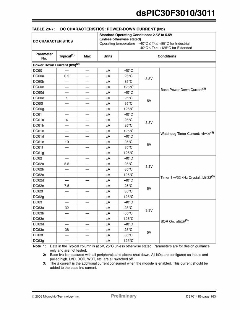
dsPIC30F3010/3011
TABLE 23-7: DC CHARACTERISTICS: POWER-DOWN CURRENT (IPD)
DC CHARACTERISTICS
Standard Operating Conditions: 2.5V to 5.5V(unless otherwise stated)Operating temperature -40°C ≤ TA ≤ +85°C for Industrial
-40°C ≤ TA ≤ +125°C for Extended
Parameter No.
Typical(1) Max Units Conditions
Power Down Current (IPD)(2)
DC60 — — μA -40°C
3.3V
Base Power Down Current(3)
DC60a 0.5 — μA 25°C
DC60b — — μA 85°C
DC60c — — μA 125°C
DC60d — — μA -40°C
5VDC60e 1 — μA 25°C
DC60f — — μA 85°C
DC60g — — μA 125°C
DC61 — — μA -40°C
3.3V
Watchdog Timer Current: ΔIWDT(3)
DC61a 4 — μA 25°C
DC61b — — μA 85°C
DC61c — — μA 125°C
DC61d — — μA -40°C
5VDC61e 10 — μA 25°C
DC61f — — μA 85°C
DC61g — — μA 125°C
DC62 — — μA -40°C
3.3V
Timer 1 w/32 kHz Crystal: ΔITI32(3)
DC62a 5.5 — μA 25°C
DC62b — — μA 85°C
DC62c — — μA 125°C
DC62d — — μA -40°C
5VDC62e 7.5 — μA 25°C
DC62f — — μA 85°C
DC62g — — μA 125°C
DC63 — — μA -40°C
3.3V
BOR On: ΔIBOR(3)
DC63a 32 — μA 25°C
DC63b — — μA 85°C
DC63c — — μA 125°C
DC63d — — μA -40°C
5VDC63e 38 — μA 25°C
DC63f — — μA 85°C
DC63g — — μA 125°C
Note 1: Data in the Typical column is at 5V, 25°C unless otherwise stated. Parameters are for design guidance only and are not tested.
2: Base IPD is measured with all peripherals and clocks shut down. All I/Os are configured as inputs and pulled high. LVD, BOR, WDT, etc. are all switched off.
3: The Δ current is the additional current consumed when the module is enabled. This current should be added to the base IPD current.
© 2005 Microchip Technology Inc. Preliminary DS70141B-page 163

dsPIC30F3010/3011
TABLE 23-8: DC CHARACTERISTICS: I/O PIN INPUT SPECIFICATIONS
DC CHARACTERISTICS
Standard Operating Conditions: 2.5V to 5.5V(unless otherwise stated)Operating temperature -40°C ≤ TA ≤ +85°C for Industrial
-40°C ≤ TA ≤ +125°C for Extended
Param No.
Symbol Characteristic Min Typ(1) Max Units Conditions
VIL Input Low Voltage(2)
DI10 I/O pins: with Schmitt Trigger buffer VSS — 0.2 VDD V
DI15 MCLR VSS — 0.2 VDD V
DI16 OSC1 (in XT, HS and LP modes) VSS — 0.2 VDD V
DI17 OSC1 (in RC mode)(3) VSS — 0.3 VDD V
DI18 SDA, SCL TBD — TBD V SMbus disabled
DI19 SDA, SCL TBD — TBD V SMbus enabled
VIH Input High Voltage(2)
DI20 I/O pins: with Schmitt Trigger buffer 0.8 VDD — VDD V
DI25 MCLR 0.8 VDD — VDD V
DI26 OSC1 (in XT, HS and LP modes) 0.7 VDD — VDD V
DI27 OSC1 (in RC mode)(3) 0.9 VDD — VDD V
DI28 SDA, SCL TBD — TBD V SMbus disabled
DI29 SDA, SCL TBD — TBD V SMbus enabled
ICNPU CNXX Pull-up Current(2)
DI30 50 250 400 μA VDD = 5V, VPIN = VSS
DI31 TBD TBD TBD μA VDD = 3V, VPIN = VSS
IIL Input Leakage Current(2)(4)(5)
DI50 I/O ports — 0.01 ±1 μA VSS ≤ VPIN ≤ VDD,Pin at hi-impedance
DI51 Analog input pins — 0.50 — μA VSS ≤ VPIN ≤ VDD,Pin at hi-impedance
DI55 MCLR — 0.05 ±5 μA VSS ≤ VPIN ≤ VDD
DI56 OSC1 — 0.05 ±5 μA VSS ≤ VPIN ≤ VDD, XT, HSand LP Osc mode
Legend: TBD = To Be DeterminedNote 1: Data in “Typ” column is at 5V, 25°C unless otherwise stated. Parameters are for design guidance only and
are not tested.2: These parameters are characterized but not tested in manufacturing.3: In RC oscillator configuration, the OSC1/CLKl pin is a Schmitt Trigger input. It is not recommended that
the dsPIC30F device be driven with an external clock while in RC mode.4: The leakage current on the MCLR pin is strongly dependent on the applied voltage level. The specified
levels represent normal operating conditions. Higher leakage current may be measured at different input voltages.
5: Negative current is defined as current sourced by the pin.
DS70141B-page 164 Preliminary © 2005 Microchip Technology Inc.

dsPIC30F3010/3011
FIGURE 23-1: BROWN-OUT RESET CHARACTERISTICS
TABLE 23-9: DC CHARACTERISTICS: I/O PIN OUTPUT SPECIFICATIONS
DC CHARACTERISTICS
Standard Operating Conditions: 2.5V to 5.5V(unless otherwise stated)Operating temperature -40°C ≤ TA ≤ +85°C for Industrial
-40°C ≤ TA ≤ +125°C for Extended
Param No.
Symbol Characteristic Min Typ(1) Max Units Conditions
VOL Output Low Voltage(2)
DO10 I/O ports — — 0.6 V IOL = 8.5 mA, VDD = 5V
— — TBD V IOL = 2.0 mA, VDD = 3V
DO16 OSC2/CLKOUT — — 0.6 V IOL = 1.6 mA, VDD = 5V
(RC or EC Osc mode) — — TBD V IOL = 2.0 mA, VDD = 3V
VOH Output High Voltage(2)
DO20 I/O ports VDD – 0.7 — — V IOH = -3.0 mA, VDD = 5V
TBD — — V IOH = -2.0 mA, VDD = 3V
DO26 OSC2/CLKOUT VDD – 0.7 — — V IOH = -1.3 mA, VDD = 5V
(RC or EC Osc mode) TBD — — V IOH = -2.0 mA, VDD = 3V
Capacitive Loading Specs on Output Pins(2)
DO50 COSC2 OSC2/SOSC2 pin — — 15 pF In XTL, XT, HS and LP modes when external clock is used to drive OSC1.
DO56 CIO All I/O pins and OSC2 — — 50 pF RC or EC Osc mode
DO58 CB SCL, SDA — — 400 pF In I2C™ mode
Legend: TBD = To Be DeterminedNote 1: Data in “Typ” column is at 5V, 25°C unless otherwise stated. Parameters are for design guidance only and
are not tested.2: These parameters are characterized but not tested in manufacturing.
BO10
RESET (due to BOR)
VDD
(Device in Brown-out Reset)
(Device not in Brown-out Reset)
Power Up Time-out
BO15
© 2005 Microchip Technology Inc. Preliminary DS70141B-page 165

dsPIC30F3010/3011
TABLE 23-10: ELECTRICAL CHARACTERISTICS: BOR
TABLE 23-11: DC CHARACTERISTICS: PROGRAM AND EEPROM
DC CHARACTERISTICS
Standard Operating Conditions: 2.5V to 5.5V(unless otherwise stated)Operating temperature -40°C ≤ TA ≤ +85°C for Industrial
-40°C ≤ TA ≤ +125°C for Extended
ParamNo.
Symbol Characteristic Min Typ(1) Max Units Conditions
BO10 VBOR BOR Voltage(2) on VDD transition high to low
BORV = 00(3) — — — V Not in operating range
BORV = 01 2.7 — 2.86 V
BORV = 10 4.2 — 4.46 V
BORV = 11 4.5 — 4.78 V
BO15 VBHYS — 5 — mV
Note 1: Data in “Typ” column is at 5V, 25°C unless otherwise stated. Parameters are for design guidance only and are not tested.
2: These parameters are characterized but not tested in manufacturing.3: 00 values not in usable operating range.
DC CHARACTERISTICS
Standard Operating Conditions: 2.5V to 5.5V(unless otherwise stated)Operating temperature -40°C ≤ TA ≤ +85°C for Industrial
-40°C ≤ TA ≤ +125°C for Extended
ParamNo.
Symbol Characteristic Min Typ(1) Max Units Conditions
Data EEPROM Memory(2)
D120 ED Byte Endurance 100K 1M — E/W -40°C ≤ TA ≤ +85°C
D121 VDRW VDD for Read/Write VMIN — 5.5 V Using EECON to read/writeVMIN = Minimum operating voltage
D122 TDEW Erase/Write Cycle Time — 2 — ms
D123 TRETD Characteristic Retention 40 100 — Year Provided no other specifications are violated
D124 IDEW IDD During Programming — 10 30 mA Row Erase
Program Flash Memory(2)
D130 EP Cell Endurance 10K 100K — E/W -40°C ≤ TA ≤ +85°C
D131 VPR VDD for Read VMIN — 5.5 V VMIN = Minimum operating voltage
D132 VEB VDD for Bulk Erase 4.5 — 5.5 V
D133 VPEW VDD for Erase/Write 3.0 — 5.5 V
D134 TPEW Erase/Write Cycle Time — 2 — ms
D135 TRETD Characteristic Retention 40 100 — Year Provided no other specifications are violated
D136 TEB ICSP Block Erase Time — 4 — ms
D137 IPEW IDD During Programming — 10 30 mA Row Erase
D138 IEB IDD During Programming — 10 30 mA Bulk Erase
Note 1: Data in “Typ” column is at 5V, 25°C unless otherwise stated.2: These parameters are characterized but not tested in manufacturing.
DS70141B-page 166 Preliminary © 2005 Microchip Technology Inc.

dsPIC30F3010/3011
23.2 AC Characteristics and Timing Parameters
The information contained in this section defines dsPIC30F AC characteristics and timing parameters.
TABLE 23-12: TEMPERATURE AND VOLTAGE SPECIFICATIONS – AC
FIGURE 23-2: LOAD CONDITIONS FOR DEVICE TIMING SPECIFICATIONS
FIGURE 23-3: EXTERNAL CLOCK TIMING
AC CHARACTERISTICS
Standard Operating Conditions: 2.5V to 5.5V(unless otherwise stated)Operating temperature -40°C ≤ TA ≤ +85°C for Industrial
-40°C ≤ TA ≤ +125°C for ExtendedOperating voltage VDD range as described in DC Spec Section 23.1 "DC Characteristics".
VDD/2
CL
RL
Pin
Pin
VSS
VSS
CL
RL = 464 ΩCL = 50 pF for all pins except OSC2
5 pF for OSC2 output
Load Condition 1 - for all pins except OSC2 Load Condition 2 - for OSC2
OSC1
CLKOUT
Q4 Q1 Q2 Q3 Q4 Q1
OS20
OS25OS30 OS30
OS40 OS41
OS31 OS31
© 2005 Microchip Technology Inc. Preliminary DS70141B-page 167

dsPIC30F3010/3011
TABLE 23-13: EXTERNAL CLOCK TIMING REQUIREMENTS
AC CHARACTERISTICS
Standard Operating Conditions: 2.5V to 5.5V(unless otherwise stated)Operating temperature -40°C ≤ TA ≤ +85°C for Industrial
-40°C ≤ TA ≤ +125°C for Extended
ParamNo.
Symbol Characteristic Min Typ(1) Max Units Conditions
OS10 FOSC External CLKIN Frequency(2)
(External clocks allowed onlyin EC mode)
DC444
————
4010107.5
MHzMHzMHzMHz
ECEC with 4x PLLEC with 8x PLLEC with 16x PLL
Oscillator Frequency(2) DC0.44444
1031——
————————8
512
44
1010107.52533——
MHzMHzMHzMHzMHzMHzMHzkHzMHzkHz
RCXTLXTXT with 4x PLLXT with 8x PLLXT with 16x PLLHSLPFRC internalLPRC internal
OS20 TOSC TOSC = 1/FOSC — — — — See parameter OS10for FOSC value
OS25 TCY Instruction Cycle Time(2)(3) 33 — DC ns See Table 23-15
OS30 TosL,TosH
External Clock(2) in (OSC1)High or Low Time
.45 x TOSC — — ns EC
OS31 TosR,TosF
External Clock(2) in (OSC1)Rise or Fall Time
— — 20 ns EC
OS40 TckR CLKOUT Rise Time(2)(4) — 6 10 ns
OS41 TckF CLKOUT Fall Time(2)(4) — 6 10 ns
Note 1: Data in “Typ” column is at 5V, 25°C unless otherwise stated. Parameters are for design guidance only and are not tested.
2: These parameters are characterized but not tested in manufacturing.3: Instruction cycle period (TCY) equals four times the input oscillator time-base period. All specified values
are based on characterization data for that particular oscillator type under standard operating conditions with the device executing code. Exceeding these specified limits may result in an unstable oscillator operation and/or higher than expected current consumption. All devices are tested to operate at “min.” values with an external clock applied to the OSC1/CLKI pin. When an external clock input is used, the “Max.” cycle time limit is “DC” (no clock) for all devices.
4: Measurements are taken in EC or ERC modes. The CLKOUT signal is measured on the OSC2 pin. CLKOUT is low for the Q1-Q2 period (1/2 TCY) and high for the Q3-Q4 period (1/2 TCY).
DS70141B-page 168 Preliminary © 2005 Microchip Technology Inc.

dsPIC30F3010/3011
TABLE 23-15: INTERNAL CLOCK TIMING EXAMPLES
TABLE 23-14: PLL CLOCK TIMING SPECIFICATIONS (VDD = 2.5 TO 5.5 V)
AC CHARACTERISTICS
Standard Operating Conditions: 2.5V to 5.5V(unless otherwise stated)Operating temperature -40°C ≤ TA ≤ +85°C for Industrial
-40°C ≤ TA ≤ +125°C for Extended
ParamNo.
Symbol Characteristic(1) Min Typ(2) Max Units Conditions
OS50 FPLLI PLL Input Frequency Range(2) 4 — 10 MHz EC, XT modes with PLL
OS51 FSYS On-chip PLL Output(2) 16 — 120 MHz EC, XT modes with PLL
OS52 TLOC PLL Start-up Time (Lock Time) — 20 50 μs
OS53 DCLK CLKOUT Stability (Jitter) TBD 1 TBD % Measured over 100 ms period
Legend: TBD = To Be DeterminedNote 1: These parameters are characterized but not tested in manufacturing.
2: Data in “Typ” column is at 5V, 25°C unless otherwise stated. Parameters are for design guidance only and are not tested.
Clock Oscillator
Mode
FOSC (MHz)(1) TCY (μsec)(2) MIPS(3)
w/o PLLMIPS(3)
w PLL x4MIPS(3)
w PLL x8MIPS(3)
w PLL x16
EC 0.200 20.0 0.05 — — —
4 1.0 1.0 4.0 8.0 16.0
10 0.4 2.5 10.0 20.0 —
25 0.16 6.25 — — —
XT 4 1.0 1.0 4.0 8.0 16.0
10 0.4 2.5 10.0 20.0 —
Note 1: Assumption: Oscillator Postscaler is divide by 1.2: Instruction Execution Cycle Time: TCY = 1/MIPS.3: Instruction Execution Frequency: MIPS = (FOSC * PLLx)/4 [since there are 4 Q clocks per instruction
cycle].
© 2005 Microchip Technology Inc. Preliminary DS70141B-page 169

dsPIC30F3010/3011
TABLE 23-16: AC CHARACTERISTICS: INTERNAL RC ACCURACY
AC CHARACTERISTICS
Standard Operating Conditions: 2.5 V to 5.5 V(unless otherwise stated)Operating temperature -40°C ≤ TA ≤ +85°C for industrial
-40°C ≤ TA ≤ +125°C for Extended
Param No.
Characteristic Min Typ Max Units Conditions
Internal FRC Accuracy @ FRC Freq = 7.5 MHz(1)
FRC TBD % +25°C VDD = 3.0-3.6 V
TBD % +25°C VDD = 4.5-5.5 V
TBD % -40°C ≤ TA ≤ +85°C VDD = 3.0-3.6 V
TBD % -40°C ≤ TA ≤ +85°C VDD = 4.5-5.5 V
TBD % -40°C ≤ TA ≤ +125°C VDD = 4.5-5.5 V
FRC with x4 PLL TBD % +25°C VDD = 3.0-3.6 V
TBD % +25°C VDD = 4.5-5.5 V
TBD % -40°C ≤ TA ≤ +85°C VDD = 3.0-3.6 V
TBD % -40°C ≤ TA ≤ +85°C VDD = 4.5-5.5 V
TBD % -40°C ≤ TA ≤ +125°C VDD = 4.5-5.5 V
FRC with x8 PLL TBD % +25°C VDD = 3.0-3.6 V
TBD % +25°C VDD = 4.5-5.5 V
TBD % -40°C ≤ TA ≤ +85°C VDD = 3.0-3.6 V
TBD % -40°C ≤ TA ≤ +85°C VDD = 4.5-5.5 V
TBD % -40°C ≤ TA ≤ +125°C VDD = 4.5-5.5 V
FRC with x16 PLL TBD % +25°C VDD = 3.0-3.6 V
TBD % +25°C VDD = 4.5-5.5 V
TBD % -40°C ≤ TA ≤ +85°C VDD = 3.0-3.6 V
TBD % -40°C ≤ TA ≤ +85°C VDD = 4.5-5.5 V
TBD % -40°C ≤ TA ≤ +125°C VDD = 4.5-5.5 V
Note 1: Frequency calibrated at 25°C and 5V. TUN bits can be used to compensate for temperature drift.
DS70141B-page 170 Preliminary © 2005 Microchip Technology Inc.
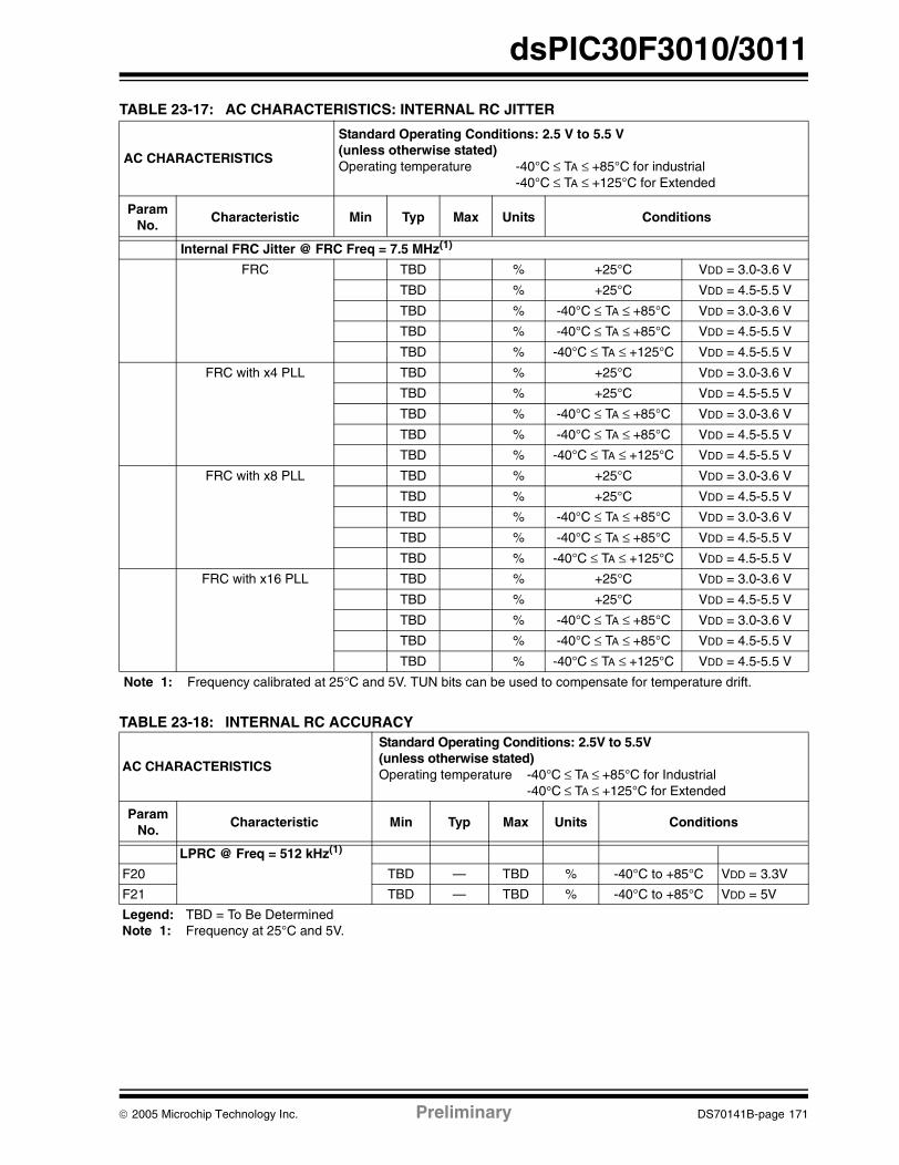
dsPIC30F3010/3011
TABLE 23-17: AC CHARACTERISTICS: INTERNAL RC JITTER
AC CHARACTERISTICS
Standard Operating Conditions: 2.5 V to 5.5 V(unless otherwise stated)Operating temperature -40°C ≤ TA ≤ +85°C for industrial
-40°C ≤ TA ≤ +125°C for Extended
Param No.
Characteristic Min Typ Max Units Conditions
Internal FRC Jitter @ FRC Freq = 7.5 MHz(1)
FRC TBD % +25°C VDD = 3.0-3.6 V
TBD % +25°C VDD = 4.5-5.5 V
TBD % -40°C ≤ TA ≤ +85°C VDD = 3.0-3.6 V
TBD % -40°C ≤ TA ≤ +85°C VDD = 4.5-5.5 V
TBD % -40°C ≤ TA ≤ +125°C VDD = 4.5-5.5 V
FRC with x4 PLL TBD % +25°C VDD = 3.0-3.6 V
TBD % +25°C VDD = 4.5-5.5 V
TBD % -40°C ≤ TA ≤ +85°C VDD = 3.0-3.6 V
TBD % -40°C ≤ TA ≤ +85°C VDD = 4.5-5.5 V
TBD % -40°C ≤ TA ≤ +125°C VDD = 4.5-5.5 V
FRC with x8 PLL TBD % +25°C VDD = 3.0-3.6 V
TBD % +25°C VDD = 4.5-5.5 V
TBD % -40°C ≤ TA ≤ +85°C VDD = 3.0-3.6 V
TBD % -40°C ≤ TA ≤ +85°C VDD = 4.5-5.5 V
TBD % -40°C ≤ TA ≤ +125°C VDD = 4.5-5.5 V
FRC with x16 PLL TBD % +25°C VDD = 3.0-3.6 V
TBD % +25°C VDD = 4.5-5.5 V
TBD % -40°C ≤ TA ≤ +85°C VDD = 3.0-3.6 V
TBD % -40°C ≤ TA ≤ +85°C VDD = 4.5-5.5 V
TBD % -40°C ≤ TA ≤ +125°C VDD = 4.5-5.5 V
Note 1: Frequency calibrated at 25°C and 5V. TUN bits can be used to compensate for temperature drift.
TABLE 23-18: INTERNAL RC ACCURACY
AC CHARACTERISTICS
Standard Operating Conditions: 2.5V to 5.5V(unless otherwise stated)Operating temperature -40°C ≤ TA ≤ +85°C for Industrial
-40°C ≤ TA ≤ +125°C for Extended
ParamNo.
Characteristic Min Typ Max Units Conditions
LPRC @ Freq = 512 kHz(1)
F20 TBD — TBD % -40°C to +85°C VDD = 3.3V
F21 TBD — TBD % -40°C to +85°C VDD = 5V
Legend: TBD = To Be DeterminedNote 1: Frequency at 25°C and 5V.
© 2005 Microchip Technology Inc. Preliminary DS70141B-page 171

dsPIC30F3010/3011
FIGURE 23-4: CLKOUT AND I/O TIMING CHARACTERISTICS
TABLE 23-19: CLKOUT AND I/O TIMING REQUIREMENTS
AC CHARACTERISTICS
Standard Operating Conditions: 2.5V to 5.5V(unless otherwise stated)Operating temperature -40°C ≤ TA ≤ +85°C for Industrial
-40°C ≤ TA ≤ +125°C for Extended
ParamNo.
Symbol Characteristic(1)(2)(3) Min Typ(4) Max Units Conditions
DO31 TIOR Port output rise time — 10 25 ns —
DO32 TIOF Port output fall time — 10 25 ns —
DI35 TINP INTx pin high or low time (output) 20 — — ns —
DI40 TRBP CNx high or low time (input) 2 TCY — — ns —
Note 1: These parameters are asynchronous events not related to any internal clock edges2: Measurements are taken in RC mode and EC mode where CLKOUT output is 4 x TOSC.3: These parameters are characterized but not tested in manufacturing.4: Data in “Typ” column is at 5V, 25°C unless otherwise stated.
Note: Refer to Figure 23-2 for load conditions.
I/O Pin(Input)
I/O Pin(Output)
DI35
Old Value New Value
DI40
DO31DO32
DS70141B-page 172 Preliminary © 2005 Microchip Technology Inc.

dsPIC30F3010/3011
FIGURE 23-5: RESET, WATCHDOG TIMER, OSCILLATOR START-UP TIMER AND POWER-UP TIMER TIMING CHARACTERISTICS
VDD
MCLR
InternalPOR
PWRTTime-out
OSCTime-out
InternalRESET
WatchdogTimer
RESET
SY11
SY10
SY20SY13
I/O Pins
SY13
Note: Refer to Figure 23-2 for load conditions.
FSCM Delay
SY35
SY30
SY12
© 2005 Microchip Technology Inc. Preliminary DS70141B-page 173

dsPIC30F3010/3011
TABLE 23-20: RESET, WATCHDOG TIMER, OSCILLATOR START-UP TIMER, POWER-UP TIMER AND BROWN-OUT RESET TIMING REQUIREMENTS
FIGURE 23-6: BAND GAP START-UP TIME CHARACTERISTICS
AC CHARACTERISTICS
Standard Operating Conditions: 2.5V to 5.5V(unless otherwise stated)Operating temperature -40°C ≤ TA ≤ +85°C for Industrial
-40°C ≤ TA ≤ +125°C for Extended
ParamNo.
Symbol Characteristic(1) Min Typ(2) Max Units Conditions
SY10 TmcL MCLR Pulse Width (low) 2 — — μs -40°C to +85°C
SY11 TPWRT Power-up Timer Period TBDTBDTBDTBD
04
1664
TBDTBDTBDTBD
ms -40°C to +85°CUser programmable
SY12 TPOR Power On Reset Delay 3 10 30 μs -40°C to +85°C
SY13 TIOZ I/O Hi-impedance from MCLR Low or Watchdog Timer Reset
— — 100 ns
SY20 TWDT1 Watchdog Timer Time-out Period (No Prescaler)
1.8 2.0 2.2 ms VDD = 5V, -40°C to +85°C
TWDT2 1.9 2.1 2.3 ms VDD = 3V, -40°C to +85°C
SY25 TBOR Brown-out Reset Pulse Width(3) 100 — — μs VDD ≤ VBOR (D034)
SY30 TOST Oscillation Start-up Timer Period — 1024 TOSC — — TOSC = OSC1 period
SY35 TFSCM Fail-Safe Clock Monitor Delay — 100 — μs -40°C to +85°C
Legend: TBD = To Be DeterminedNote 1: These parameters are characterized but not tested in manufacturing.
2: Data in “Typ” column is at 5V, 25°C unless otherwise stated.3: Refer to Figure 23-1 and Table 23-10 for BOR.
VBGAP
Enable Band Gap
Band Gap
0V
(see Note)
Stable
Note: Band gap is enabled when FBORPOR<7> is set.
SY40
DS70141B-page 174 Preliminary © 2005 Microchip Technology Inc.

dsPIC30F3010/3011
TABLE 23-21: BAND GAP START-UP TIME REQUIREMENTS
FIGURE 23-7: TIMER 1, 2, 3, 4 AND 5 EXTERNAL CLOCK TIMING CHARACTERISTICS
AC CHARACTERISTICS
Standard Operating Conditions: 2.5V to 5.5V(unless otherwise stated)Operating temperature -40°C ≤ TA ≤ +85°C for Industrial
-40°C ≤ TA ≤ +125°C for Extended
ParamNo.
Symbol Characteristic(1) Min Typ(2) Max Units Conditions
SY40 TBGAP Band Gap Start-up Time — 20 50 μs Defined as the time between the instant that the band gap is enabled and the moment that the band gap reference voltage is stable. RCON<13>Status bit
Note 1: These parameters are characterized but not tested in manufacturing.2: Data in “Typ” column is at 5V, 25°C unless otherwise stated.
Note: Refer to Figure 23-2 for load conditions.
Tx11
Tx15
Tx10
Tx20
TMRX
OS60
TxCK
© 2005 Microchip Technology Inc. Preliminary DS70141B-page 175

dsPIC30F3010/3011
TABLE 23-22: TIMER1 EXTERNAL CLOCK TIMING REQUIREMENTS
TABLE 23-23: TIMER2 AND TIMER4 EXTERNAL CLOCK TIMING REQUIREMENTS
AC CHARACTERISTICS
Standard Operating Conditions: 2.5V to 5.5V(unless otherwise stated)Operating temperature -40°C ≤ TA ≤ +85°C for Industrial
-40°C ≤ TA ≤ +125°C for Extended
ParamNo.
Symbol Characteristic Min Typ Max Units Conditions
TA10 TTXH TxCK High Time Synchronous,no prescaler
0.5 TCY + 20 — — ns Must also meet parameter TA15
Synchronous,with prescaler
10 — — ns
Asynchronous 10 — — ns
TA11 TTXL TxCK Low Time Synchronous,no prescaler
0.5 TCY + 20 — — ns Must also meet parameter TA15
Synchronous,with prescaler
10 — — ns
Asynchronous 10 — — ns
TA15 TTXP TxCK Input Period Synchronous,no prescaler
TCY + 10 — — ns
Synchronous,with prescaler
Greater of:20 ns or
(TCY + 40)/N
— — — N = prescale value(1, 8, 64, 256)
Asynchronous 20 — — ns
OS60 Ft1 SOSC1/T1CK oscillator input frequency range (oscillator enabled by setting bit TCS (T1CON, bit 1))
DC — 50 kHz
TA20 TCKEXTMRL Delay from External TxCK Clock Edge to Timer Increment
2 TOSC 6 TOSC —
AC CHARACTERISTICS
Standard Operating Conditions: 2.5V to 5.5V(unless otherwise stated)Operating temperature -40°C ≤ TA ≤ +85°C for Industrial
-40°C ≤ TA ≤ +125°C for Extended
ParamNo.
Symbol Characteristic Min Typ Max Units Conditions
TB10 TtxH TxCK High Time Synchronous,no prescaler
0.5 TCY + 20 — — ns Must also meet parameter TB15
Synchronous,with prescaler
10 — — ns
TB11 TtxL TxCK Low Time Synchronous,no prescaler
0.5 TCY + 20 — — ns Must also meet parameter TB15
Synchronous,with prescaler
10 — — ns
TB15 TtxP TxCK Input Period Synchronous,no prescaler
TCY + 10 — — ns N = prescale value(1, 8, 64, 256)Synchronous,
with prescalerGreater of:
20 ns or(TCY + 40)/N
TB20 TCKEXTMRL Delay from External TxCK Clock Edge to Timer Increment
2 TOSC — 6 TOSC —
DS70141B-page 176 Preliminary © 2005 Microchip Technology Inc.

dsPIC30F3010/3011
TABLE 23-24: TIMER3 AND TIMER5 EXTERNAL CLOCK TIMING REQUIREMENTS
FIGURE 23-8: TIMERQ (QEI MODULE) EXTERNAL CLOCK TIMING CHARACTERISTICS
TABLE 23-25: QEI MODULE EXTERNAL CLOCK TIMING REQUIREMENTS
AC CHARACTERISTICS
Standard Operating Conditions: 2.5V to 5.5V(unless otherwise stated)Operating temperature -40°C ≤ TA ≤ +85°C for Industrial
-40°C ≤ TA ≤ +125°C for Extended
ParamNo.
Symbol Characteristic Min Typ Max Units Conditions
TC10 TtxH TxCK High Time Synchronous 0.5 TCY + 20 — — ns Must also meet parameter TC15
TC11 TtxL TxCK Low Time Synchronous 0.5 TCY + 20 — — ns Must also meet parameter TC15
TC15 TtxP TxCK Input Period Synchronous,no prescaler
TCY + 10 — — ns N = prescalevalue (1, 8, 64, 256)Synchronous,
with prescalerGreater of:
20 ns or (TCY + 40)/N
TC20 TCKEXTMRL Delay from External TxCK Clock Edge to Timer Increment
2 TOSC — 6 TOSC —
AC CHARACTERISTICS
Standard Operating Conditions: 2.5V to 5.5V(unless otherwise stated)Operating temperature -40°C ≤ TA ≤ +85°C for Industrial
-40°C ≤ TA ≤ +125°C for Extended
ParamNo.
Symbol Characteristic(1) Min Typ Max Units Conditions
TQ10 TtQH TQCK High Time Synchronous,with prescaler
TCY + 20 — ns Must also meet parameter TQ15
TQ11 TtQL TQCK Low Time Synchronous,with prescaler
TCY + 20 — ns Must also meet parameter TQ15
TQ15 TtQP TQCP Input Period Synchronous,with prescaler
2 * TCY + 40 — ns —
TQ20 TCKEXTMRL Delay from External TQCK Clock Edge to Timer Increment
Tosc 5 Tosc ns —
Note 1: These parameters are characterized but not tested in manufacturing.
TQ11
TQ15
TQ10
TQ20
QEB
POSCNT
© 2005 Microchip Technology Inc. Preliminary DS70141B-page 177

dsPIC30F3010/3011
FIGURE 23-9: INPUT CAPTURE (CAPx) TIMING CHARACTERISTICS
TABLE 23-26: INPUT CAPTURE TIMING REQUIREMENTS
FIGURE 23-10: OUTPUT COMPARE MODULE (OCx) TIMING CHARACTERISTICS
TABLE 23-27: OUTPUT COMPARE MODULE TIMING REQUIREMENTS
AC CHARACTERISTICS
Standard Operating Conditions: 2.5V to 5.5V(unless otherwise stated)Operating temperature -40°C ≤ TA ≤ +85°C for Industrial
-40°C ≤ TA ≤ +125°C for Extended
ParamNo.
Symbol Characteristic(1) Min Max Units Conditions
IC10 TccL ICx Input Low Time No Prescaler 0.5 TCY + 20 — ns
With Prescaler 10 — ns
IC11 TccH ICx Input High Time No Prescaler 0.5 TCY + 20 — ns
With Prescaler 10 — ns
IC15 TccP ICx Input Period (2 TCY + 40)/N — ns N = prescale value (1, 4, 16)
Note 1: These parameters are characterized but not tested in manufacturing.
AC CHARACTERISTICS
Standard Operating Conditions: 2.5V to 5.5V(unless otherwise stated)Operating temperature -40°C ≤ TA ≤ +85°C for Industrial
-40°C ≤ TA ≤ +125°C for Extended
Param No.
Symbol Characteristic(1) Min Typ(2) Max Units Conditions
OC10 TccF OCx Output Fall Time — 10 25 ns —
OC11 TccR OCx Output Rise Time — 10 25 ns —
Note 1: These parameters are characterized but not tested in manufacturing.2: Data in “Typ” column is at 5V, 25°C unless otherwise stated. Parameters are for design guidance only and
are not tested.
ICX
IC10 IC11
IC15
Note: Refer to Figure 23-2 for load conditions.
OCx
OC11 OC10(Output Compare
Note: Refer to Figure 23-2 for load conditions.
or PWM Mode)
DS70141B-page 178 Preliminary © 2005 Microchip Technology Inc.

dsPIC30F3010/3011
FIGURE 23-11: OC/PWM MODULE TIMING CHARACTERISTICS
TABLE 23-28: SIMPLE OC/PWM MODE TIMING REQUIREMENTS
AC CHARACTERISTICS
Standard Operating Conditions: 2.5V to 5.5V(unless otherwise stated)Operating temperature -40°C ≤ TA ≤ +85°C for Industrial
-40°C ≤ TA ≤ +125°C for Extended
Param No.
Symbol Characteristic(1) Min Typ(2) Max Units Conditions
OC15 TFD Fault Input to PWM I/O Change
— — 25 ns VDD = 3V -40°C to +85°C
TBD ns VDD = 5V
OC20 TFLT Fault Input Pulse Width — — 50 ns VDD = 3V -40°C to +85°C
TBD ns VDD = 5V
Legend: TBD = To Be DeterminedNote 1: These parameters are characterized but not tested in manufacturing.
2: Data in “Typ” column is at 5V, 25°C unless otherwise stated. Parameters are for design guidance only and are not tested.
OCFA/OCFB
OCx
OC20
OC15
© 2005 Microchip Technology Inc. Preliminary DS70141B-page 179

dsPIC30F3010/3011
FIGURE 23-12: MOTOR CONTROL PWM MODULE FAULT TIMING CHARACTERISTICS
FIGURE 23-13: MOTOR CONTROL PWM MODULE TIMING CHARACTERISTICS
TABLE 23-29: MOTOR CONTROL PWM MODULE TIMING REQUIREMENTS
AC CHARACTERISTICS
Standard Operating Conditions: 2.5V to 5.5V(unless otherwise stated)Operating temperature -40°C ≤ TA ≤ +85°C for Industrial
-40°C ≤ TA ≤ +125°C for Extended
ParamNo.
Symbol Characteristic(1) Min Typ(2) Max Units Conditions
MP10 TFPWM PWM Output Fall Time — 10 25 ns VDD = 5V -40°C to +85°C
MP11 TRPWM PWM Output Rise Time — 10 25 ns VDD = 5V -40°C to +85°C
MP12 TFPWM PWM Output Fall Time — TBD TBD ns VDD = 3V -40°C to +85°C
MP13 TRPWM PWM Output Rise Time — TBD TBD ns VDD = 3V -40°C to +85°C
MP20TFD Fault Input ↓ to PWM
I/O Change— — 25 ns VDD = 3V -40°C to +85°C
TBD ns VDD = 5V
MP30TFH Minimum Pulse Width — — 50 ns VDD = 3V -40°C to +85°C
TBD ns VDD = 5V
Legend: TBD = To Be DeterminedNote 1: These parameters are characterized but not tested in manufacturing.
2: Data in “Typ” column is at 5V, 25°C unless otherwise stated. Parameters are for design guidance only and are not tested.
FLTA/B
PWMx
MP30
MP20
PWMx
MP11 MP10
Note: Refer to Figure 23-2 for load conditions.
DS70141B-page 180 Preliminary © 2005 Microchip Technology Inc.

dsPIC30F3010/3011
FIGURE 23-14: QEA/QEB INPUT CHARACTERISTICS
TABLE 23-30: QUADRATURE DECODER TIMING REQUIREMENTS
AC CHARACTERISTICS
Standard Operating Conditions: 2.5V to 5.5V(unless otherwise stated)Operating temperature -40°C ≤ TA ≤ +85°C for Industrial
-40°C ≤ TA ≤ +125°C for Extended
ParamNo.
Symbol Characteristic(1) Typ(2) Max Units Conditions
TQ30 TQUL Quadrature Input Low Time 6 TCY — ns —
TQ31 TQUH Quadrature Input High Time 6 TCY — ns —
TQ35 TQUIN Quadrature Input Period 12 TCY — ns —
TQ36 TQUP Quadrature Phase Period 3 TCY — ns —
TQ40 TQUFL Filter Time to Recognize Low,with Digital Filter
3 * N * TCY — ns N = 1, 2, 4, 16, 32, 64, 128 and 256 (Note 2)
TQ41 TQUFH Filter Time to Recognize High,with Digital Filter
3 * N * TCY — ns N = 1, 2, 4, 16, 32, 64, 128 and 256 (Note 2)
Note 1: These parameters are characterized but not tested in manufacturing.2: N = Index Channel Digital Filter Clock Divide Select Bits. Refer to Section 16. “Quadrature Encoder
Interface (QEI)” in the dsPIC30F Family Reference Manual, (DS70046).
TQ30
TQ35
TQ31
QEA (input)
TQ30
TQ35
TQ31
QEB (input)
TQ36
QEB Internal
TQ40TQ41
© 2005 Microchip Technology Inc. Preliminary DS70141B-page 181

dsPIC30F3010/3011
FIGURE 23-15: QEI MODULE INDEX PULSE TIMING CHARACTERISTICS
TABLE 23-31: QEI INDEX PULSE TIMING REQUIREMENTS
AC CHARACTERISTICS
Standard Operating Conditions: 2.5V to 5.5V(unless otherwise stated)Operating temperature -40°C ≤ TA ≤ +85°C for Industrial
-40°C ≤ TA ≤ +125°C for Extended
ParamNo.
Symbol Characteristic(1) Min Max Units Conditions
TQ50 TqIL Filter Time to Recognize Low,with Digital Filter
3 * N * TCY — ns N = 1, 2, 4, 16, 32, 64,128 and 256 (Note 2)
TQ51 TqiH Filter Time to Recognize High,with Digital Filter
3 * N * TCY — ns N = 1, 2, 4, 16, 32, 64,128 and 256 (Note 2)
TQ55 Tqidxr Index Pulse Recognized to PositionCounter Reset (Ungated Index)
3 TCY — ns —
Note 1: These parameters are characterized but not tested in manufacturing.2: Alignment of Index Pulses to QEA and QEB is shown for Position Counter reset timing only. Shown for
forward direction only (QEA leads QEB). Same timing applies for reverse direction (QEA lags QEB) but Index Pulse recognition occurs on falling edge.
QEA(input)
UngatedIndex
QEB(input)
TQ55
Index Internal
Position
TQ50TQ51
DS70141B-page 182 Preliminary © 2005 Microchip Technology Inc.

dsPIC30F3010/3011
FIGURE 23-16: SPI™ MODULE MASTER MODE (CKE = 0) TIMING CHARACTERISTICS
TABLE 23-32: SPI™ MASTER MODE (CKE = 0) TIMING REQUIREMENTS
AC CHARACTERISTICS
Standard Operating Conditions: 2.5V to 5.5V(unless otherwise stated)Operating temperature -40°C ≤ TA ≤ +85°C for Industrial
-40°C ≤ TA ≤ +125°C for Extended
ParamNo.
Symbol Characteristic(1) Min Typ(2) Max Units Conditions
SP10 TscL SCKX Output Low Time(3) TCY / 2 — — ns —
SP11 TscH SCKX Output High Time(3) TCY / 2 — — ns —
SP20 TscF SCKX Output Fall Time(4 — 10 25 ns —
SP21 TscR SCKX Output Rise Time(4) — 10 25 ns —
SP30 TdoF SDOX Data Output Fall Time(4) — 10 25 ns —
SP31 TdoR SDOX Data Output Rise Time(4) — 10 25 ns —
SP35 TscH2doV,TscL2doV
SDOX Data Output Valid after SCKX Edge
— — 30 ns —
SP40 TdiV2scH,TdiV2scL
Setup Time of SDIX Data Inputto SCKX Edge
20 — — ns —
SP41 TscH2diL,TscL2diL
Hold Time of SDIX Data Inputto SCKX Edge
20 — — ns —
Note 1: These parameters are characterized but not tested in manufacturing.2: Data in “Typ” column is at 5V, 25°C unless otherwise stated. Parameters are for design guidance only and
are not tested.3: The minimum clock period for SCK is 100 ns. Therefore, the clock generated in Master mode must not
violate this specification.4: Assumes 50 pF load on all SPI pins.
SCKx(CKP = 0)
SCKx(CKP = 1)
SDOx
SDIx
SP11 SP10
SP40 SP41
SP21SP20SP35
SP20SP21
MSb LSbBIT14 - - - - - -1
MSb IN LSb INBIT14 - - - -1
SP30SP31
Note: Refer to Figure 23-2 for load conditions.
© 2005 Microchip Technology Inc. Preliminary DS70141B-page 183

dsPIC30F3010/3011
FIGURE 23-17: SPI™ MODULE MASTER MODE (CKE =1) TIMING CHARACTERISTICS
TABLE 23-33: SPI™ MODULE MASTER MODE (CKE = 1) TIMING REQUIREMENTS
AC CHARACTERISTICS
Standard Operating Conditions: 2.5V to 5.5V(unless otherwise stated)Operating temperature -40°C ≤ TA ≤ +85°C for Industrial
-40°C ≤ TA ≤ +125°C for Extended
ParamNo.
Symbol Characteristic(1) Min Typ(2) Max Units Conditions
SP10 TscL SCKX output low time(3) TCY / 2 — — ns —
SP11 TscH SCKX output high time(3) TCY / 2 — — ns —
SP20 TscF SCKX output fall time(4) — 10 25 ns —
SP21 TscR SCKX output rise time(4) — 10 25 ns —
SP30 TdoF SDOX data output fall time(4) — 10 25 ns —
SP31 TdoR SDOX data output rise time(4) — 10 25 ns —
SP35 TscH2doV,TscL2doV
SDOX data output valid afterSCKX edge
— — 30 ns —
SP36 TdoV2sc, TdoV2scL
SDOX data output setup tofirst SCKX edge
30 — — ns —
SP40 TdiV2scH, TdiV2scL
Setup time of SDIX data inputto SCKX edge
20 — — ns —
SP41 TscH2diL, TscL2diL
Hold time of SDIX data inputto SCKX edge
20 — — ns —
Note 1: These parameters are characterized but not tested in manufacturing.2: Data in “Typ” column is at 5V, 25°C unless otherwise stated. Parameters are for design guidance only and
are not tested.3: The minimum clock period for SCK is 100 ns. Therefore, the clock generated in master mode must not
violate this specification.4: Assumes 50 pF load on all SPI pins.
SCKX
(CKP = 0)
SCKX
(CKP = 1)
SDOX
SDIX
SP36
SP30,SP31
SP35
MSb
MSb IN
BIT14 - - - - - -1
LSb INBIT14 - - - -1
LSb
Note: Refer to Figure 23-2 for load conditions.
SP11 SP10 SP20SP21
SP21SP20
SP40
SP41
DS70141B-page 184 Preliminary © 2005 Microchip Technology Inc.
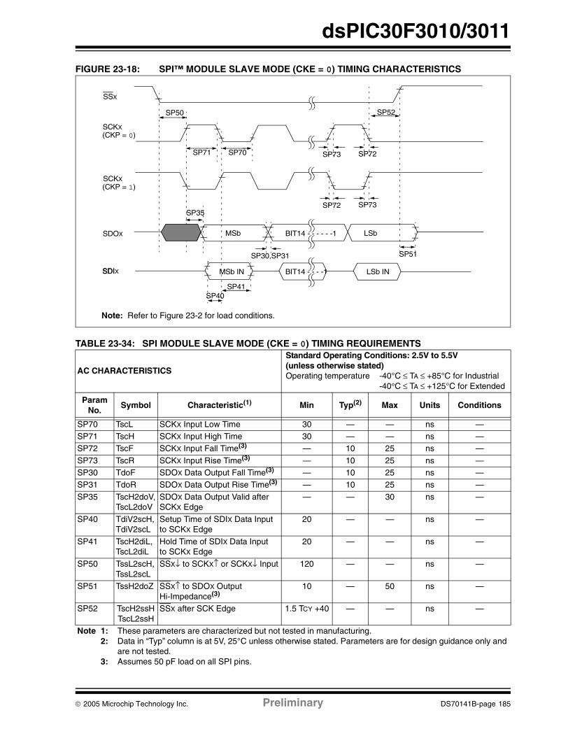
dsPIC30F3010/3011
FIGURE 23-18: SPI™ MODULE SLAVE MODE (CKE = 0) TIMING CHARACTERISTICS
TABLE 23-34: SPI MODULE SLAVE MODE (CKE = 0) TIMING REQUIREMENTS
AC CHARACTERISTICS
Standard Operating Conditions: 2.5V to 5.5V(unless otherwise stated)Operating temperature -40°C ≤ TA ≤ +85°C for Industrial
-40°C ≤ TA ≤ +125°C for Extended
ParamNo.
Symbol Characteristic(1) Min Typ(2) Max Units Conditions
SP70 TscL SCKX Input Low Time 30 — — ns —SP71 TscH SCKX Input High Time 30 — — ns —SP72 TscF SCKX Input Fall Time(3) — 10 25 ns —
SP73 TscR SCKX Input Rise Time(3) — 10 25 ns —SP30 TdoF SDOX Data Output Fall Time(3) — 10 25 ns —SP31 TdoR SDOX Data Output Rise Time(3) — 10 25 ns —
SP35 TscH2doV,TscL2doV
SDOX Data Output Valid afterSCKX Edge
— — 30 ns —
SP40 TdiV2scH, TdiV2scL
Setup Time of SDIX Data Inputto SCKX Edge
20 — — ns —
SP41 TscH2diL, TscL2diL
Hold Time of SDIX Data Inputto SCKX Edge
20 — — ns —
SP50 TssL2scH, TssL2scL
SSX↓ to SCKX↑ or SCKX↓ Input 120 — — ns —
SP51 TssH2doZ SSX↑ to SDOX OutputHi-Impedance(3)
10 — 50 ns —
SP52 TscH2ssHTscL2ssH
SSX after SCK Edge 1.5 TCY +40 — — ns —
Note 1: These parameters are characterized but not tested in manufacturing.2: Data in “Typ” column is at 5V, 25°C unless otherwise stated. Parameters are for design guidance only and
are not tested.3: Assumes 50 pF load on all SPI pins.
SSX
SCKX(CKP = 0)
SCKX(CKP = 1)
SDOX
SDI
SP50
SP40SP41
SP30,SP31 SP51
SP35
SDIX
MSb LSbBIT14 - - - - - -1
MSb IN BIT14 - - - -1 LSb IN
SP52
SP73SP72
SP72SP73SP71 SP70
Note: Refer to Figure 23-2 for load conditions.
© 2005 Microchip Technology Inc. Preliminary DS70141B-page 185
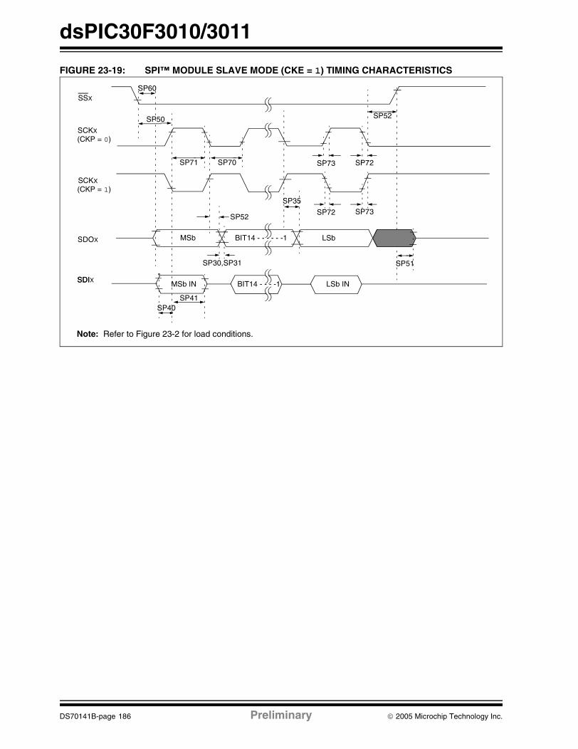
dsPIC30F3010/3011
FIGURE 23-19: SPI™ MODULE SLAVE MODE (CKE = 1) TIMING CHARACTERISTICS
SSX
SCKX
(CKP = 0)
SCKX
(CKP = 1)
SDOX
SDI
SP50
SP60
SDIX
SP30,SP31
MSb BIT14 - - - - - -1 LSb
SP51
MSb IN BIT14 - - - -1 LSb IN
SP35
SP52
SP52
SP73SP72
SP72SP73SP71 SP70
SP40SP41
Note: Refer to Figure 23-2 for load conditions.
DS70141B-page 186 Preliminary © 2005 Microchip Technology Inc.

dsPIC30F3010/3011
TABLE 23-35: SPI™ MODULE SLAVE MODE (CKE = 1) TIMING REQUIREMENTS
AC CHARACTERISTICS
Standard Operating Conditions: 2.5V to 5.5V(unless otherwise stated)Operating temperature -40°C ≤ TA ≤ +85°C for Industrial
-40°C ≤ TA ≤ +125°C for Extended
ParamNo.
Symbol Characteristic(1) Min Typ(2) Max Units Conditions
SP70 TscL SCKX Input Low Time 30 — — ns —
SP71 TscH SCKX Input High Time 30 — — ns —
SP72 TscF SCKX Input Fall Time(3) — 10 25 ns —
SP73 TscR SCKX Input Rise Time(3) — 10 25 ns —
SP30 TdoF SDOX Data Output Fall Time(3) — 10 25 ns —
SP31 TdoR SDOX Data Output Rise Time(3) — 10 25 ns —
SP35 TscH2doV,TscL2doV
SDOX Data Output Valid afterSCKX Edge
— — 30 ns —
SP40 TdiV2scH, TdiV2scL
Setup Time of SDIX Data Inputto SCKX Edge
20 — — ns —
SP41 TscH2diL, TscL2diL
Hold Time of SDIX Data Inputto SCKX Edge
20 — — ns —
SP50 TssL2scH, TssL2scL
SSX↓ to SCKX↓ or SCKX↑ input 120 — — ns —
SP51 TssH2doZ SS↑ to SDOX OutputHi-Impedance(4)
10 — 50 ns —
SP52 TscH2ssHTscL2ssH
SSX↑ after SCKX Edge 1.5 TCY + 40 — — ns —
SP60 TssL2doV SDOX Data Output Valid afterSSX Edge
— — 50 ns —
Note 1: These parameters are characterized but not tested in manufacturing.2: Data in “Typ” column is at 5V, 25°C unless otherwise stated. Parameters are for design guidance only and
are not tested.3: The minimum clock period for SCK is 100 ns. Therefore, the clock generated in Master mode must not
violate this specification.4: Assumes 50 pF load on all SPI pins.
© 2005 Microchip Technology Inc. Preliminary DS70141B-page 187
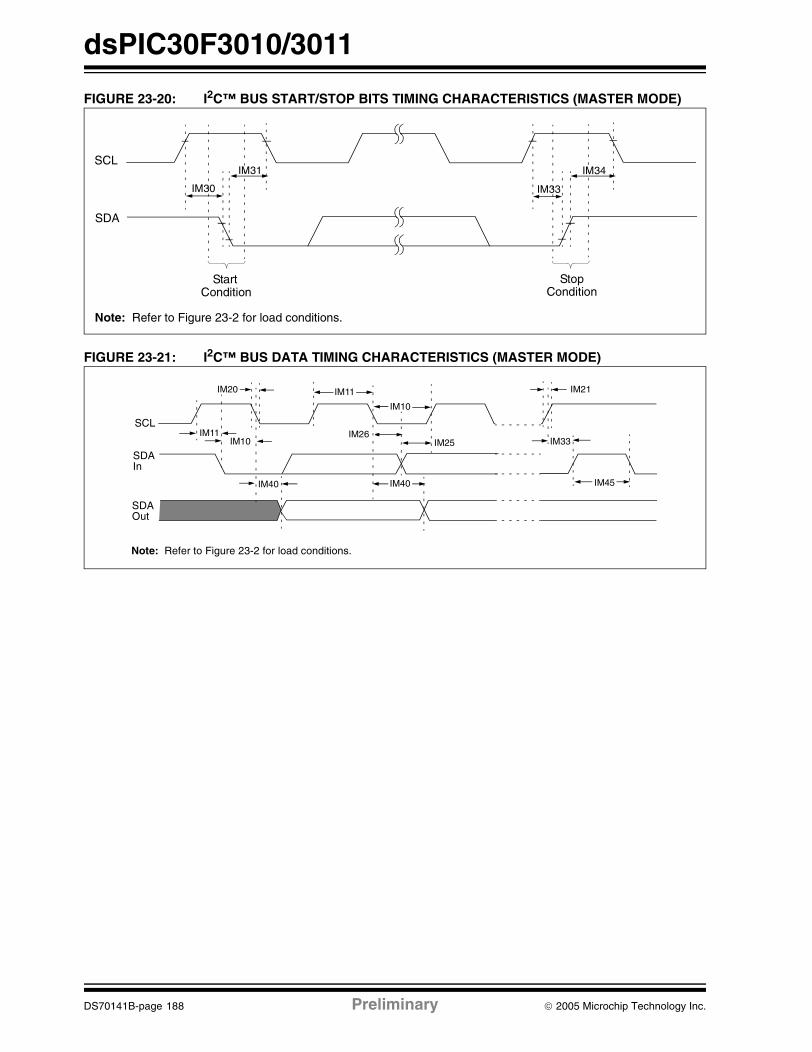
dsPIC30F3010/3011
FIGURE 23-20: I2C™ BUS START/STOP BITS TIMING CHARACTERISTICS (MASTER MODE)
FIGURE 23-21: I2C™ BUS DATA TIMING CHARACTERISTICS (MASTER MODE)
IM31 IM34SCL
SDA
StartCondition
StopCondition
IM30 IM33
Note: Refer to Figure 23-2 for load conditions.
IM11IM10 IM33
IM11
IM10
IM20
IM26IM25
IM40 IM40 IM45
IM21
SCL
SDAIn
SDAOut
Note: Refer to Figure 23-2 for load conditions.
DS70141B-page 188 Preliminary © 2005 Microchip Technology Inc.

dsPIC30F3010/3011
TABLE 23-36: I2C™ BUS DATA TIMING REQUIREMENTS (MASTER MODE)
AC CHARACTERISTICS
Standard Operating Conditions: 2.5V to 5.5V(unless otherwise stated)Operating temperature -40°C ≤ TA ≤ +85°C for Industrial
-40°C ≤ TA ≤ +125°C for Extended
ParamNo.
Symbol Characteristic Min(1) Max Units Conditions
IM10 TLO:SCL Clock Low Time 100 kHz mode TCY / 2 (BRG + 1) — μs —
400 kHz mode TCY / 2 (BRG + 1) — μs —
1 MHz mode(2) TCY / 2 (BRG + 1) — μs —
IM11 THI:SCL Clock High Time 100 kHz mode TCY / 2 (BRG + 1) — μs —
400 kHz mode TCY / 2 (BRG + 1) — μs —
1 MHz mode(2) TCY / 2 (BRG + 1) — μs —
IM20 TF:SCL SDA and SCLFall Time
100 kHz mode — 300 ns CB is specified to be from 10 to 400 pF400 kHz mode 20 + 0.1 CB 300 ns
1 MHz mode(2) — 100 ns
IM21 TR:SCL SDA and SCLRise Time
100 kHz mode — 1000 ns CB is specified to be from 10 to 400 pF400 kHz mode 20 + 0.1 CB 300 ns
1 MHz mode(2) — 300 ns
IM25 TSU:DAT Data InputSetup Time
100 kHz mode 250 — ns —
400 kHz mode 100 — ns
1 MHz mode(2) TBD — ns
IM26 THD:DAT Data InputHold Time
100 kHz mode 0 — ns —
400 kHz mode 0 0.9 μs
1 MHz mode(2) TBD — ns
IM30 TSU:STA Start ConditionSetup Time
100 kHz mode TCY / 2 (BRG + 1) — μs Only relevant for repeated Startcondition
400 kHz mode TCY / 2 (BRG + 1) — μs
1 MHz mode(2) TCY / 2 (BRG + 1) — μs
IM31 THD:STA Start Condition Hold Time
100 kHz mode TCY / 2 (BRG + 1) — μs After this period thefirst clock pulse isgenerated
400 kHz mode TCY / 2 (BRG + 1) — μs
1 MHz mode(2) TCY / 2 (BRG + 1) — μs
IM33 TSU:STO Stop Condition Setup Time
100 kHz mode TCY / 2 (BRG + 1) — μs —
400 kHz mode TCY / 2 (BRG + 1) — μs
1 MHz mode(2) TCY / 2 (BRG + 1) — μs
IM34 THD:STO Stop Condition 100 kHz mode TCY / 2 (BRG + 1) — ns —
Hold Time 400 kHz mode TCY / 2 (BRG + 1) — ns
1 MHz mode(2) TCY / 2 (BRG + 1) — ns
IM40 TAA:SCL Output Valid From Clock
100 kHz mode — 3500 ns —
400 kHz mode — 1000 ns —
1 MHz mode(2) — — ns —
IM45 TBF:SDA Bus Free Time 100 kHz mode 4.7 — μs Time the bus must be free before a newtransmission can start
400 kHz mode 1.3 — μs
1 MHz mode(2) TBD — μs
IM50 CB Bus Capacitive Loading — 400 pF
Note 1: BRG is the value of the I2C™ Baud Rate Generator. Refer to Section 21 “Inter-Integrated Circuit (I2C)” in the dsPIC30F Family Reference Manual, (DS70046).
2: Maximum pin capacitance = 10 pF for all I2C pins (for 1 MHz mode only).
© 2005 Microchip Technology Inc. Preliminary DS70141B-page 189

dsPIC30F3010/3011
FIGURE 23-22: I2C™ BUS START/STOP BITS TIMING CHARACTERISTICS (SLAVE MODE)
FIGURE 23-23: I2C™ BUS DATA TIMING CHARACTERISTICS (SLAVE MODE)
IS31 IS34SCL
SDA
StartCondition
StopCondition
IS30 IS33
IS30IS31 IS33
IS11
IS10
IS20
IS26IS25
IS40 IS40 IS45
IS21
SCL
SDAIn
SDAOut
DS70141B-page 190 Preliminary © 2005 Microchip Technology Inc.

dsPIC30F3010/3011
TABLE 23-37: I2C™ BUS DATA TIMING REQUIREMENTS (SLAVE MODE)
AC CHARACTERISTICS
Standard Operating Conditions: 2.5V to 5.5V(unless otherwise stated)Operating temperature -40°C ≤ TA ≤ +85°C for Industrial
-40°C ≤ TA ≤ +125°C for Extended
ParamNo.
Symbol Characteristic Min Max Units Conditions
IS10 TLO:SCL Clock Low Time 100 kHz mode 4.7 — μs Device must operate at a minimum of 1.5 MHz
400 kHz mode 1.3 — μs Device must operate at a minimum of 10 MHz.
1 MHz mode(1) 0.5 — μs —
IS11 THI:SCL Clock High Time 100 kHz mode 4.0 — μs Device must operate at a minimum of 1.5 MHz
400 kHz mode 0.6 — μs Device must operate at a minimum of 10 MHz
1 MHz mode(1) 0.5 — μs —
IS20 TF:SCL SDA and SCLFall Time
100 kHz mode — 300 ns CB is specified to be from10 to 400 pF400 kHz mode 20 + 0.1 CB 300 ns
1 MHz mode(1) — 100 ns
IS21 TR:SCL SDA and SCLRise Time
100 kHz mode — 1000 ns CB is specified to be from10 to 400 pF400 kHz mode 20 + 0.1 CB 300 ns
1 MHz mode(1) — 300 ns
IS25 TSU:DAT Data InputSetup Time
100 kHz mode 250 — ns —
400 kHz mode 100 — ns
1 MHz mode(1) 100 — ns
IS26 THD:DAT Data InputHold Time
100 kHz mode 0 — ns —
400 kHz mode 0 0.9 μs
1 MHz mode(1) 0 0.3 μs
IS30 TSU:STA Start ConditionSetup Time
100 kHz mode 4.7 — μs Only relevant for repeated Start condition400 kHz mode 0.6 — μs
1 MHz mode(1) 0.25 — μs
IS31 THD:STA Start Condition Hold Time
100 kHz mode 4.0 — μs After this period the first clock pulse is generated400 kHz mode 0.6 — μs
1 MHz mode(1) 0.25 — μs
IS33 TSU:STO Stop Condition Setup Time
100 kHz mode 4.7 — μs —
400 kHz mode 0.6 — μs
1 MHz mode(1) 0.6 — μs
IS34 THD:STO Stop Condition 100 kHz mode 4000 — ns —
Hold Time 400 kHz mode 600 — ns
1 MHz mode(1) 250 ns
IS40 TAA:SCL Output Valid From Clock
100 kHz mode 0 3500 ns —
400 kHz mode 0 1000 ns
1 MHz mode(1) 0 350 ns
IS45 TBF:SDA Bus Free Time 100 kHz mode 4.7 — μs Time the bus must be free before a new transmission can start
400 kHz mode 1.3 — μs
1 MHz mode(1) 0.5 — μs
IS50 CB Bus Capacitive Loading
— 400 pF —
Note 1: Maximum pin capacitance = 10 pF for all I2C™ pins (for 1 MHz mode only).
© 2005 Microchip Technology Inc. Preliminary DS70141B-page 191

dsPIC30F3010/3011
FIGURE 23-24: CAN MODULE I/O TIMING CHARACTERISTICS
TABLE 23-38: CAN MODULE I/O TIMING REQUIREMENTS
AC CHARACTERISTICS
Standard Operating Conditions: 2.5V to 5.5V(unless otherwise stated)Operating temperature -40°C ≤ TA ≤ +85°C for Industrial
-40°C ≤ TA ≤ +125°C for Extended
ParamNo.
Symbol Characteristic(1) Min Typ(2) Max Units Conditions
CA10 TioF Port Output Fall Time — 10 25 ns —
CA11 TioR Port Output Rise Time — 10 25 ns —
CA20 Tcwf Pulse Width to TriggerCAN Wakeup Filter
500 ns —
Note 1: These parameters are characterized but not tested in manufacturing.2: Data in “Typ” column is at 5V, 25°C unless otherwise stated. Parameters are for design guidance only and
are not tested.
CXTX Pin(output)
CA10 CA11
Old Value New Value
CA20
CXRX Pin(input)
DS70141B-page 192 Preliminary © 2005 Microchip Technology Inc.

dsPIC30F3010/3011
TABLE 23-39: 10-BIT HIGH-SPEED A/D MODULE SPECIFICATIONS
AC CHARACTERISTICS
Standard Operating Conditions: 2.5V to 5.5V(unless otherwise stated)Operating temperature -40°C ≤ TA ≤ +85°C for Industrial
-40°C ≤ TA ≤ +125°C for Extended
Param No.
Symbol Characteristic Min. Typ Max. Units Conditions
Device Supply
AD01 AVDD Module VDD Supply Greater ofVDD - 0.3
or 2.7
Lesser ofVDD + 0.3
or 5.5
V —
AD02 AVSS Module VSS Supply Vss - 0.3 VSS + 0.3 V —
Reference Inputs
AD05 VREFH Reference Voltage High AVss+2.7 AVDD V —
AD06 VREFL Reference Voltage Low AVss AVDD - 2.7 V —
AD07 VREF Absolute Reference Voltage AVss - 0.3 AVDD + 0.3 V —
AD08 IREF Current Drain — 200.001
3003
μAμA
A/D operatingA/D off
Analog Input
AD10 VINH-VINL Full-Scale Input Span VREFL VREFH V —
AD11 VIN Absolute Input Voltage AVSS - 0.3 AVDD + 0.3 V —
AD12 — Leakage Current — ±0.001 ±0.244 μA VINL = AVSS = VREFL = 0V,AVDD = VREFH = 5VSource Impedance = 5 kΩ
AD13 — Leakage Current — ±0.001 ±0.244 μA VINL = AVSS = VREFL = 0V,AVDD = VREFH = 3VSource Impedance = 5 kΩ
AD15 RSS Switch Resistance — 5K — Ω —
AD16 CSAMPLE Sample Capacitor — 2.5 pF —
AD17 RIN Recommended ImpedanceOf Analog Voltage Source
— 5K Ω —
DC Accuracy
AD20 Nr Resolution 10 data bits bits —
AD21 INL Integral Nonlinearity — ±0.5 < ±1 LSb VINL = AVSS = VREFL = 0V,AVDD = VREFH = 5V
AD21A INL Integral Nonlinearity — ±0.5 < ±1 LSb VINL = AVSS = VREFL = 0V,AVDD = VREFH = 3V
AD22 DNL Differential Nonlinearity — ±0.5 < ±1 LSb VINL = AVSS = VREFL = 0V, AVDD = VREFH = 5V
AD22A DNL Differential Nonlinearity — ±0.5 < ±1 LSb VINL = AVSS = VREFL = 0V, AVDD = VREFH = 3V
AD23 GERR Gain Error — ±0.75 TBD LSb VINL = AVSS = VREFL = 0V, AVDD = VREFH = 5V
AD23A GERR Gain Error — ±0.75 TBD LSb VINL = AVSS = VREFL = 0V, AVDD = VREFH = 3V
Legend: TBD = To Be DeterminedNote 1: The A/D conversion result never decreases with an increase in the input voltage, and has no missing
codes.
© 2005 Microchip Technology Inc. Preliminary DS70141B-page 193

dsPIC30F3010/3011
AD24 EOFF Offset Error — ±0.75 TBD LSb VINL = AVSS = VREFL = 0V, AVDD = VREFH = 5V
AD24A EOFF Offset Error — ±0.75 TBD LSb VINL = AVSS = VREFL = 0V, AVDD = VREFH = 3V
AD25 — Monotonicity(1) — — — — Guaranteed
AD26 CMRR Common-Mode Rejection — TBD — dB —
AD27 PSRR Power Supply Rejection Ratio
— TBD — dB —
AD28 CTLK Channel to Channel Crosstalk
— TBD — dB —
Dynamic Performance
AD30 THD Total Harmonic Distortion — TBD — dB —
AD31 SINAD Signal to Noise andDistortion
— TBD — dB —
AD32 SFDR Spurious Free Dynamic Range
— TBD — dB —
AD33 FNYQ Input Signal Bandwidth — — 250 kHz —
AD34 ENOB Effective Number of Bits — TBD TBD bits —
TABLE 23-39: 10-BIT HIGH-SPEED A/D MODULE SPECIFICATIONS (CONTINUED)
AC CHARACTERISTICS
Standard Operating Conditions: 2.5V to 5.5V(unless otherwise stated)Operating temperature -40°C ≤ TA ≤ +85°C for Industrial
-40°C ≤ TA ≤ +125°C for Extended
Param No.
Symbol Characteristic Min. Typ Max. Units Conditions
Legend: TBD = To Be DeterminedNote 1: The A/D conversion result never decreases with an increase in the input voltage, and has no missing
codes.
DS70141B-page 194 Preliminary © 2005 Microchip Technology Inc.

dsPIC30F3010/3011
FIGURE 23-25: 10-BIT HIGH-SPEED A/D CONVERSION TIMING CHARACTERISTICS(CHPS = 01, SIMSAM = 0, ASAM = 0, SSRC = 000)
AD55TSAMP
CLEAR SAMPSET SAMP
AD61
ADCLK
Instruction
SAMP
ch0_dischrg
ch1_samp
AD60
DONE
ADIF
ADRES(0)
ADRES(1)
1 2 3 4 5 6 9 5 6 8
1 - Software sets ADCON. SAMP to start sampling.
2 - Sampling starts after discharge period.
3 - Software clears ADCON. SAMP to start conversion.
4 - Sampling ends, conversion sequence starts.
5 - Convert bit 9.
9 - One TAD for end of conversion.
AD50
ch0_samp
ch1_dischrg
eoc
8
AD55
9
6 - Convert bit 8.
8 - Convert bit 0.
Execution
TSAMP is described in the dsPIC30F MCU Family Reference Manual, (DS70046), Section 17, “10-bit A/D Converter”.
© 2005 Microchip Technology Inc. Preliminary DS70141B-page 195
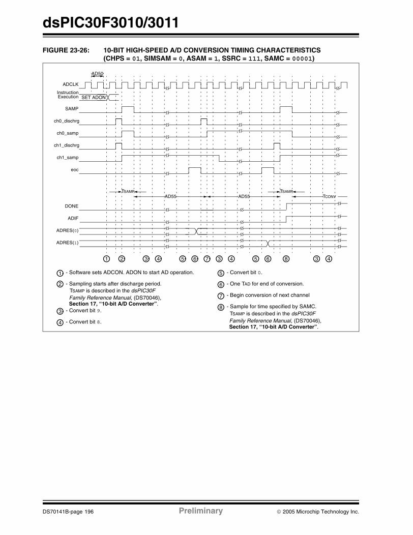
dsPIC30F3010/3011
FIGURE 23-26: 10-BIT HIGH-SPEED A/D CONVERSION TIMING CHARACTERISTICS(CHPS = 01, SIMSAM = 0, ASAM = 1, SSRC = 111, SAMC = 00001)
AD55TSAMP
SET ADON
ADCLK
Instruction
SAMP
ch0_dischrg
ch1_samp
DONE
ADIF
ADRES(0)
ADRES(1)
1 2 3 4 5 6 4 5 6 8
1 - Software sets ADCON. ADON to start AD operation.
2 - Sampling starts after discharge period.
3 - Convert bit 9.
4 - Convert bit 8.
5 - Convert bit 0.
AD50
ch0_samp
ch1_dischrg
eoc
7 3
AD55
6 - One TAD for end of conversion.
7 - Begin conversion of next channel
8 - Sample for time specified by SAMC.
TSAMPTCONV
3 4
Execution
TSAMP is described in the dsPIC30F Family Reference Manual, (DS70046),
TSAMP is described in the dsPIC30F Family Reference Manual, (DS70046),
Section 17, “10-bit A/D Converter”.
Section 17, “10-bit A/D Converter”.
DS70141B-page 196 Preliminary © 2005 Microchip Technology Inc.

dsPIC30F3010/3011
TABLE 23-40: 10-BIT HIGH-SPEED A/D CONVERSION TIMING REQUIREMENTS
AC CHARACTERISTICS
Standard Operating Conditions: 2.5V to 5.5V(unless otherwise stated)Operating temperature -40°C ≤ TA ≤ +85°C for Industrial
-40°C ≤ TA ≤ +125°C for Extended
Param No.
Symbol Characteristic Min. Typ Max. Units Conditions
Clock Parameters
AD50 TAD A/D Clock Period 154256
ns VDD = 5V (Note 1)VDD = 2.7V (Note 1)
AD51 tRC A/D Internal RC Oscillator Period 700 900 1100 ns —
Conversion Rate
AD55 tCONV Conversion Time 13 TAD ns —
AD56 FCNV Throughput Rate 500100
kspsksps
VDD = VREF = 5VVDD = VREF = 2.7V
AD57 TSAMP Sample Time — 1 TAD — ns VDD = 3-5.5V
Timing Parameters
AD60 tPCS Conversion Start from SampleTrigger
— — TAD ns —
AD61 tPSS Sample Start from SettingSample (SAMP) Bit
0.5 TAD — 1.5 TAD ns —
AD62 tCSS Conversion Completion toSample Start (ASAM = 1)
— — TBD ns —
AD63 tDPU Time to Stabilize Analog Stage from A/D Off to A/D On
— — TBD μs —
Legend: TBD = To Be DeterminedNote 1: Because the sample caps will eventually lose charge, clock periods above 100 μsec can affect linearity
performance, especially at elevated temperatures.
© 2005 Microchip Technology Inc. Preliminary DS70141B-page 197

dsPIC30F3010/3011
NOTES:
DS70141B-page 198 Preliminary © 2005 Microchip Technology Inc.
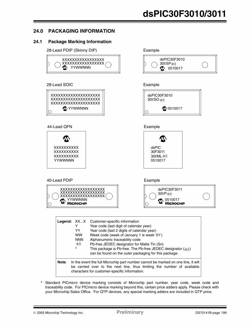
dsPIC30F3010/3011
24.0 PACKAGING INFORMATION
24.1 Package Marking Information
28-Lead PDIP (Skinny DIP)
XXXXXXXXXXXXXXXXXXXXXXXXXXXXXXXXXX
YYWWNNN
Example
dsPIC30F3010
0510017
28-Lead SOIC
XXXXXXXXXXXXXXXXXXXXXXXXXXXXXXXXXXXXXXXXXXXXXXXXXXXXXXXXXXXX
YYWWNNN
Example
dsPIC30F3010
0510017
XXXXXXXXXX
44-Lead QFN
XXXXXXXXXXXXXXXXXXXXYYWWNNN
dsPIC
Example
051001730I/ML
Example
dsPIC30F3011
0510017
40-Lead PDIP
XXXXXXXXXXXXXXXXXXXXXXXXXXXXXXXXXXXX
XXXXXXXXXXXXXXXXXXYYWWNNN
30I/SP 3e
3e
3e
3e30I/SO
30F3011
30I/P
* Standard PICmicro device marking consists of Microchip part number, year code, week code andtraceability code. For PICmicro device marking beyond this, certain price adders apply. Please check withyour Microchip Sales Office. For QTP devices, any special marking adders are included in QTP price.
Legend: XX...X Customer-specific informationY Year code (last digit of calendar year)YY Year code (last 2 digits of calendar year)WW Week code (week of January 1 is week ‘01’)NNN Alphanumeric traceability code Pb-free JEDEC designator for Matte Tin (Sn)* This package is Pb-free. The Pb-free JEDEC designator ( )
can be found on the outer packaging for this package.
Note: In the event the full Microchip part number cannot be marked on one line, it willbe carried over to the next line, thus limiting the number of availablecharacters for customer-specific information.
3e
3e
© 2005 Microchip Technology Inc. Preliminary DS70141B-page 199

dsPIC30F3010/3011
Package Marking Information (Continued)
44-Lead TQFP
XXXXXXXXXXXXXXXXXXXXXXXXXXXXXX
YYWWNNN
Example
XXXXXXXXXX
44-Lead QFN
XXXXXXXXXXXXXXXXXXXXYYWWNNN
Example
dsPIC
051001730I/PT30F3011
3e
dsPIC
051001730I/ML30F3011
3e
DS70141B-page 200 Preliminary © 2005 Microchip Technology Inc.

dsPIC30F3010/3011
24.2 Package Details
28-Lead Skinny Plastic Dual In-line – 300 mil Body (PDIP)
1510515105βMold Draft Angle Bottom
1510515105αMold Draft Angle Top
10.928.898.13.430.350.320eBOverall Row Spacing §
0.560.480.41.022.019.016BLower Lead Width
1.651.331.02.065.053.040B1Upper Lead Width
0.380.290.20.015.012.008cLead Thickness
3.433.303.18.135.130.125LTip to Seating Plane
35.1834.6734.161.3851.3651.345DOverall Length
7.497.246.99.295.285.275E1Molded Package Width
8.267.877.62.325.310.300EShoulder to Shoulder Width
0.38.015A1Base to Seating Plane
3.433.303.18.135.130.125A2Molded Package Thickness
4.063.813.56.160.150.140ATop to Seating Plane
2.54.100pPitch
2828nNumber of Pins
MAXNOMMINMAXNOMMINDimension Limits
MILLIMETERSINCHES*Units
2
1
D
n
E1
c
eB
β
E
α
p
L
A2
B
B1
A
A1
Notes:
JEDEC Equivalent: MO-095Drawing No. C04-070
* Controlling Parameter
Dimension D and E1 do not include mold flash or protrusions. Mold flash or protrusions shall not exceed .010” (0.254mm) per side.
§ Significant Characteristic
© 2005 Microchip Technology Inc. Preliminary DS70141B-page 201

dsPIC30F3010/3011
28-Lead Plastic Small Outline – Wide, 300 mil Body (SOIC)
Foot Angle Top φ 0 4 8 0 4 8
1512015120βMold Draft Angle Bottom1512015120αMold Draft Angle Top
0.510.420.36.020.017.014BLead Width0.330.280.23.013.011.009cLead Thickness
1.270.840.41.050.033.016LFoot Length0.740.500.25.029.020.010hChamfer Distance
18.0817.8717.65.712.704.695DOverall Length7.597.497.32.299.295.288E1Molded Package Width
10.6710.3410.01.420.407.394EOverall Width0.300.200.10.012.008.004A1Standoff §2.392.312.24.094.091.088A2Molded Package Thickness2.642.502.36.104.099.093AOverall Height
1.27.050pPitch2828nNumber of Pins
MAXNOMMINMAXNOMMINDimension LimitsMILLIMETERSINCHES*Units
21
D
p
n
B
E
E1
L
c
β
45°
h
φ
A2
α
A
A1
* Controlling Parameter
Notes:Dimensions D and E1 do not include mold flash or protrusions. Mold flash or protrusions shall not exceed .010” (0.254mm) per side.JEDEC Equivalent: MS-013Drawing No. C04-052
§ Significant Characteristic
DS70141B-page 202 Preliminary © 2005 Microchip Technology Inc.

dsPIC30F3010/3011
40-Lead Plastic Dual In-line – 600 mil Body (PDIP)
1510515105βMold Draft Angle Bottom1510515105αMold Draft Angle Top
17.2716.5115.75.680.650.620eBOverall Row Spacing §0.560.460.36.022.018.014BLower Lead Width1.781.270.76.070.050.030B1Upper Lead Width0.380.290.20.015.012.008cLead Thickness3.433.303.05.135.130.120LTip to Seating Plane
52.4552.2651.942.0652.0582.045DOverall Length14.2213.8413.46.560.545.530E1Molded Package Width15.8815.2415.11.625.600.595EShoulder to Shoulder Width
0.38.015A1Base to Seating Plane4.063.813.56.160.150.140A2Molded Package Thickness4.834.454.06.190.175.160ATop to Seating Plane
2.54.100pPitch4040nNumber of Pins
MAXNOMMINMAXNOMMINDimension LimitsMILLIMETERSINCHES*Units
A2
12
D
n
E1
c
βeB
E
α
p
L
B
B1
A
A1
* Controlling Parameter
Notes:Dimensions D and E1 do not include mold flash or protrusions. Mold flash or protrusions shall not exceed .010” (0.254mm) per side.JEDEC Equivalent: MO-011Drawing No. C04-016
§ Significant Characteristic
© 2005 Microchip Technology Inc. Preliminary DS70141B-page 203
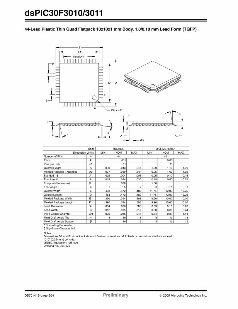
dsPIC30F3010/3011
44-Lead Plastic Thin Quad Flatpack 10x10x1 mm Body, 1.0/0.10 mm Lead Form (TQFP)
* Controlling Parameter
Notes:Dimensions D1 and E1 do not include mold flash or protrusions. Mold flash or protrusions shall not exceed .010” (0.254mm) per side.JEDEC Equivalent: MS-026Drawing No. C04-076
1.140.890.64.045.035.025CHPin 1 Corner Chamfer
1.00.039(F)Footprint (Reference)
(F)
A
A1 A2
α
E
E1
#leads=n1
p
B
D1 D
n
12
φ
c
βL
Units INCHES MILLIMETERS*Dimension Limits MIN NOM MAX MIN NOM MAX
Number of Pins n 44 44Pitch p .031 0.80
Overall Height A .039 .043 .047 1.00 1.10 1.20Molded Package Thickness A2 .037 .039 .041 0.95 1.00 1.05Standoff § A1 .002 .004 .006 0.05 0.10 0.15Foot Length L .018 .024 .030 0.45 0.60 0.75
Foot Angle φ 0 3.5 7 0 3.5 7Overall Width E .463 .472 .482 11.75 12.00 12.25Overall Length D .463 .472 .482 11.75 12.00 12.25Molded Package Width E1 .390 .394 .398 9.90 10.00 10.10Molded Package Length D1 .390 .394 .398 9.90 10.00 10.10
Pins per Side n1 11 11
Lead Thickness c .004 .006 .008 0.09 0.15 0.20Lead Width B .012 .015 .017 0.30 0.38 0.44
Mold Draft Angle Top α 5 10 15 5 10 15Mold Draft Angle Bottom β 5 10 15 5 10 15
CH x 45 °
§ Significant Characteristic
DS70141B-page 204 Preliminary © 2005 Microchip Technology Inc.

dsPIC30F3010/3011
44-Lead Plastic Quad Flat No Lead Package 8x8 mm Body (QFN)
© 2005 Microchip Technology Inc. Preliminary DS70141B-page 205
dsPIC30F3010/3011
NOTES:
DS70141B-page 206 Preliminary © 2005 Microchip Technology Inc.

dsPIC30F3010/3011
INDEX
Numerics10-bit High Speed A/D
A/D Acquisition Requirements .................................. 125Aborting a Conversion .............................................. 124ADCHS ..................................................................... 121ADCON1 ................................................................... 121ADCON2 ................................................................... 121ADCON3 ................................................................... 121ADCSSL.................................................................... 121ADPCFG................................................................... 121Configuring Analog Port Pins.................................... 127Connection Considerations....................................... 127Conversion Operation ............................................... 123Effects of a Reset...................................................... 126Operation During CPU Idle Mode ............................. 126Operation During CPU Sleep Mode.......................... 126Output Formats ......................................................... 126Power-down Modes .................................................. 126Programming the Start of Conversion Trigger .......... 124Register Map............................................................. 128Result Buffer ............................................................. 123Sampling Requirements............................................ 125Selecting the Conversion Clock ................................ 124Selecting the Conversion Sequence......................... 123
10-Bit High Speed Analog-to-Digital (A/D) Converter Module121
16-bit Up/Down Position Counter Mode.............................. 86Count Direction Status ................................................ 86Error Checking ............................................................ 86
AAC Characteristics ............................................................ 167
Load Conditions ........................................................ 167AC Temperature and Voltage Specifications .................... 167Address Generator Units .................................................... 35Alternate 16-bit Timer/Counter............................................ 87Alternate Vector Table ........................................................ 45Assembler
MPASM Assembler................................................... 151Automatic Clock Stretch.................................................... 108
During 10-bit Addressing (STREN = 1)..................... 108During 7-bit Addressing (STREN = 1)....................... 108Receive Mode ........................................................... 108Transmit Mode .......................................................... 108
BBandgap Start-up Time
Requirements............................................................ 175Timing Characteristics .............................................. 174
Barrel Shifter ....................................................................... 22Bit-Reversed Addressing .................................................... 38
Example ...................................................................... 38Implementation ........................................................... 38Modifier Values (table) ................................................ 39Sequence Table (16-Entry)......................................... 39
Block Diagrams10-bit High Speed A/D Functional............................. 12216-bit Timer1 Module .................................................. 6416-bit Timer4............................................................... 7416-bit Timer5............................................................... 7532-bit Timer4/5............................................................ 73Dedicated Port Structure............................................. 57DSP Engine ................................................................ 19
dsPIC30F3010.............................................................. 9dsPIC30F3011.............................................................. 8External Power-on Reset Circuit .............................. 137I2C ............................................................................ 106Input Capture Mode.................................................... 77Oscillator System...................................................... 131Output Compare Mode ............................................... 81PWM Module .............................................................. 92Quadrature Encoder Interface .................................... 85Reset System ........................................................... 135Shared Port Structure................................................. 58SPI............................................................................ 102SPI Master/Slave Connection................................... 102UART Receiver......................................................... 114UART Transmitter..................................................... 113
BOR Characteristics ......................................................... 166BOR. See Brown-out ResetBrown-out Reset
Characteristics.......................................................... 165Timing Requirements ............................................... 174
Brown-out Reset (BOR).................................................... 129
CC Compilers
MPLAB C17.............................................................. 152MPLAB C18.............................................................. 152MPLAB C30.............................................................. 152
CAN ModuleI/O Timing Characteristics ........................................ 192I/O Timing Requirements.......................................... 192
Center Aligned PWM .......................................................... 95CLKOUT and I/O Timing
Characteristics.......................................................... 172Requirements ........................................................... 172
Code ExamplesData EEPROM Block Erase ....................................... 54Data EEPROM Block Write ........................................ 56Data EEPROM Read.................................................. 53Data EEPROM Word Erase ....................................... 54Data EEPROM Word Write ........................................ 55Erasing a Row of Program Memory ........................... 49Initiating a Programming Sequence ........................... 50Loading Write Latches................................................ 50
Code Protection................................................................ 129Complementary PWM Operation........................................ 95Configuring Analog Port Pins.............................................. 58Control Registers ................................................................ 48
NVMADR .................................................................... 48NVMADRU ................................................................. 48NVMCON.................................................................... 48NVMKEY .................................................................... 48
Core Overview.................................................................... 15Core Register Map.............................................................. 31Customer Change Notification Service............................. 211Customer Notification Service .......................................... 211Customer Support............................................................. 211
DData Access from Program Memory Using
Program Space Visibility............................................. 26Data Accumulators and Adder/Subtractor .......................... 20
Data Space Write Saturation ...................................... 22Overflow and Saturation ............................................. 20
© 2005 Microchip Technology Inc. Preliminary DS70141B-page 207

dsPIC30F3010/3011
Round Logic................................................................ 21Write Back................................................................... 21
Data Address Space ........................................................... 27Alignment .................................................................... 30Alignment (Figure) ...................................................... 30Effect of Invalid Memory Accesses ............................. 30MCU and DSP (MAC Class) Instructions
Example .............................................................. 29Memory Map ......................................................... 27, 28Near Data Space ........................................................ 31Software Stack............................................................ 31Spaces ........................................................................ 30Width........................................................................... 30
Data EEPROM Memory ...................................................... 53Erasing........................................................................ 54Erasing, Block ............................................................. 54Erasing, Word ............................................................. 54Protection Against Spurious Write .............................. 56Reading....................................................................... 53Write Verify ................................................................. 56Writing......................................................................... 55Writing, Block .............................................................. 56Writing, Word .............................................................. 55
DC Characteristics ............................................................ 157BOR .......................................................................... 166Brown-out Reset ....................................................... 165I/O Pin Input Specifications ....................................... 164I/O Pin Output Specifications .................................... 165Idle Current (IIDLE) .................................................... 161Operating Current (IDD)............................................. 159Power-Down Current (IPD) ........................................ 163Program and EEPROM............................................. 166Temperature and Voltage Specifications .................. 157
Dead-Time Generators ....................................................... 96Ranges........................................................................ 96
Demonstration BoardsPICDEM 1 ................................................................. 154PICDEM 17 ............................................................... 155PICDEM 18R ............................................................ 155PICDEM 2 Plus ......................................................... 154PICDEM 3 ................................................................. 154PICDEM 4 ................................................................. 154PICDEM LIN ............................................................. 155PICDEM USB............................................................ 155PICDEM.net Internet/Ethernet .................................. 154
Development Support ....................................................... 151Device Configuration
Register Map............................................................. 142Device Configuration Registers......................................... 140
FBORPOR ................................................................ 140FGS........................................................................... 140FOSC ........................................................................ 140FWDT........................................................................ 140
Device Overview ................................................................... 7Divide Support..................................................................... 18DSP Engine......................................................................... 18
Multiplier...................................................................... 20dsPIC30F3010 Port Register Map ...................................... 59dsPIC30F3011 Port Register Map ...................................... 60Dual Output Compare Match Mode .................................... 82
Continuous Pulse Mode.............................................. 82Single Pulse Mode ...................................................... 82
EEdge Aligned PWM............................................................. 94Electrical Characteristics .................................................. 157
AC............................................................................. 167DC ............................................................................ 157
EquationsA/D Conversion Clock............................................... 124Baud Rate................................................................. 117PWM Period................................................................ 94PWM Resolution ......................................................... 94Serial Clock Rate ...................................................... 110
Errata .................................................................................... 6Evaluation and Programming Tools.................................. 155Exception Processing
Interrupt Priority .......................................................... 42Exception Sequence
Trap Sources .............................................................. 43External Clock Timing Characteristics
Type 1, 2, 3, 4 and 5 Timer....................................... 175External Clock Timing Requirements ............................... 168
Timer1 ...................................................................... 176Timer2 and Timer 4 .................................................. 176Timer3 and Timer5 ................................................... 177
External Interrupt Requests ................................................ 45
FFast Context Saving ........................................................... 45Flash Program Memory ...................................................... 47
In-Circuit Serial Programming (ICSP)......................... 47Run Time Self-Programming (RTSP) ......................... 47Table Instruction Operation Summary ........................ 47
II/O Pin Specifications
Input.......................................................................... 164Output ....................................................................... 165
I/O Ports.............................................................................. 57Parallel I/O (PIO) ........................................................ 57
I2C 10-bit Slave Mode Operation...................................... 107Reception ................................................................. 108Transmission ............................................................ 108
I2C 7-bit Slave Mode Operation........................................ 107Reception ................................................................. 107Transmission ............................................................ 107
I2C Master ModeBaud Rate Generator ............................................... 110Clock Arbitration ....................................................... 110Multi-Master Communication, Bus Collision and
Bus Arbitration .................................................. 110Reception ................................................................. 110Transmission ............................................................ 109
I2C ModuleAddresses................................................................. 107Bus Data Timing Characteristics
Master Mode..................................................... 188Slave Mode....................................................... 190
Bus Data Timing RequirementsMaster Mode..................................................... 189Slave Mode....................................................... 191
Bus Start/Stop Bits Timing CharacteristicsMaster Mode..................................................... 188Slave Mode....................................................... 190
DS70141B-page 208 Preliminary © 2005 Microchip Technology Inc.

dsPIC30F3010/3011
General Call Address Support .................................. 109Interrupts................................................................... 109IPMI Support ............................................................. 109Master Operation ...................................................... 109Master Support ......................................................... 109Operating Function Description ................................ 105Operation During CPU Sleep and Idle Modes .......... 110Pin Configuration ...................................................... 105Programmer’s Model................................................. 105Register Map............................................................. 111Registers................................................................... 105Slope Control ............................................................ 109Software Controlled Clock Stretching (STREN = 1).. 108Various Modes .......................................................... 105
Idle Current (IIDLE) ............................................................ 161In-Circuit Serial Programming (ICSP) ............................... 129Independent PWM Output .................................................. 97Initialization Condition for RCON Register Case 1 ........... 138Initialization Condition for RCON Register Case 2 ........... 138Input Capture (CAPX) Timing Characteristics .................. 178Input Capture Interrupts ...................................................... 79
Register Map............................................................... 80Input Capture Module ......................................................... 77
In CPU Sleep Mode .................................................... 78Simple Capture Event Mode ....................................... 78
Input Capture Timing Requirements ................................. 178Input Change Notification Module....................................... 61
Register Map (bits 7-0) ............................................... 61Input Characteristics
QEA/QEB.................................................................. 181Instruction Addressing Modes............................................. 35
File Register Instructions ............................................ 35Fundamental Modes Supported.................................. 35MAC Instructions......................................................... 36MCU Instructions ........................................................ 35Move and Accumulator Instructions............................ 36Other Instructions........................................................ 36
Instruction Set Overview ................................................... 146Instruction Set Summary................................................... 143Internal Clock Timing Examples ....................................... 169Internet Address................................................................ 211Interrupt Controller
Register Map............................................................... 46Interrupt Priority
Traps........................................................................... 43Interrupt Sequence ............................................................. 45
Interrupt Stack Frame ................................................. 45Interrupts............................................................................. 41
LLoad Conditions ................................................................ 167
MMemory Organization.......................................................... 23Microchip Internet Web Site .............................................. 211Modulo Addressing ............................................................. 36
Applicability ................................................................. 38Operation Example ..................................................... 37Start and End Address................................................ 37W Address Register Selection .................................... 37
Motor Control PWM Module................................................ 91Fault Timing Characteristics ..................................... 180Timing Characteristics .............................................. 180Timing Requirements................................................ 180
MPLAB ASM30 Assembler, Linker, Librarian ................... 152
MPLAB ICD 2 In-Circuit Debugger ................................... 153MPLAB ICE 2000 High-Performance Universal
In-Circuit Emulator.................................................... 153MPLAB ICE 4000 High-Performance Universal
In-Circuit Emulator.................................................... 153MPLAB Integrated Development Environment
Software ................................................................... 151MPLAB PM3 Device Programmer .................................... 153MPLINK Object Linker/MPLIB Object Librarian ................ 152
OOC/PWM Module Timing Characteristics ......................... 179Operating Current (IDD) .................................................... 159Oscillator
Operating Modes (Table).......................................... 130Oscillator Configurations................................................... 132
Fail-Safe Clock Monitor ............................................ 134Fast RC (FRC).......................................................... 133Initial Clock Source Selection ................................... 132Low-Power RC (LPRC) ............................................ 133LP Oscillator Control................................................. 133Phase Locked Loop (PLL) ........................................ 133Start-up Timer (OST)................................................ 132
Oscillator Selection ........................................................... 129Oscillator Start-up Timer
Timing Characteristics .............................................. 173Timing Requirements ............................................... 174
Output Compare Interrupts ................................................. 83Output Compare Mode
Register Map .............................................................. 84Output Compare Module .................................................... 81
Timing Characteristics .............................................. 178Timing Requirements ............................................... 178
Output Compare Operation During CPU Idle Mode ........... 83Output Compare Sleep Mode Operation ............................ 83
PPackaging......................................................................... 199
Marking..................................................................... 199PICkit 1 Flash Starter Kit .................................................. 155PICSTART Plus Development Programmer..................... 154Pinout Descriptions....................................................... 10, 12PLL Clock Timing Specifications ...................................... 169POR. See Power-on ResetPort Write/Read Example ................................................... 58Position Measurement Mode.............................................. 87Power Saving Modes........................................................ 139
Idle............................................................................ 140Sleep ........................................................................ 139
Power Saving Modes (Sleep and Idle) ............................. 129Power-Down Current (IPD)................................................ 163Power-on Reset (POR)..................................................... 129
Oscillator Start-up Timer (OST)................................ 129Power-up Timer (PWRT) .......................................... 129
Power-up TimerTiming Characteristics .............................................. 173Timing Requirements ............................................... 174
PRO MATE II Universal Device Programmer ................... 153Program Address Space..................................................... 23
Construction ............................................................... 24Data Access From Program Memory Using
Table Instructions ............................................... 25Data Access from, Address Generation ..................... 24Memory Map............................................................... 23
© 2005 Microchip Technology Inc. Preliminary DS70141B-page 209

dsPIC30F3010/3011
Table InstructionsTBLRDH.............................................................. 25TBLRDL .............................................................. 25TBLWTH ............................................................. 25TBLWTL.............................................................. 25
Program and EEPROM Characteristics ............................ 166Program Counter................................................................. 16Program Data Table Access ............................................... 26Program Space Visibility
Window into Program Space Operation...................... 27Programmable................................................................... 129Programmable Digital Noise Filters..................................... 87Programmer’s Model........................................................... 16
Diagram ...................................................................... 17Programming Operations .................................................... 49
Algorithm for Program Flash ....................................... 49Erasing a Row of Program Memory ............................ 49Initiating the Programming Sequence......................... 50Loading Write Latches ................................................ 50
Protection Against Accidental Writes to OSCCON ........... 134PWM
Register Map............................................................. 100PWM Duty Cycle Comparison Units ................................... 95
Duty Cycle Register Buffers........................................ 95PWM Fault Pins .................................................................. 98
Enable Bits .................................................................. 98Fault States................................................................. 98Modes ......................................................................... 98
Cycle-by-Cycle.................................................... 98Latched ............................................................... 98
PWM Operation During CPU Idle Mode.............................. 99PWM Operation During CPU Sleep Mode .......................... 99PWM Output and Polarity Control ....................................... 98
Output Pin Control ...................................................... 98PWM Output Override......................................................... 97
Complementary Output Mode..................................... 97Synchronization .......................................................... 97
PWM Period ........................................................................ 94PWM Special Event Trigger ................................................ 99
Postscaler ................................................................... 99PWM Time Base ................................................................. 93
Continuous Up/Down Counting Modes....................... 93Double Update Mode .................................................. 94Free Running Mode .................................................... 93Postscaler ................................................................... 94Prescaler ..................................................................... 94Single Shot Mode........................................................ 93
PWM Update Lockout ......................................................... 99
QQEA/QEB Input Characteristics ........................................ 181QEI Module
External Clock Timing Requirements........................ 177Index Pulse Timing Characteristics........................... 182Index Pulse Timing Requirements ............................ 182Operation During CPU Idle Mode ............................... 88Operation During CPU Sleep Mode............................ 87Register Map............................................................... 89Timer Operation During CPU Idle Mode ..................... 88Timer Operation During CPU Sleep Mode.................. 87
Quadrature Decoder Timing Requirements ...................... 181Quadrature Encoder Interface (QEI) Module ...................... 85Quadrature Encoder Interface Interrupts ............................ 88Quadrature Encoder Interface Logic ................................... 86
RReset ........................................................................ 129, 135Reset Sequence ................................................................. 43
Reset Sources ............................................................ 43Reset Timing Characteristics............................................ 173Reset Timing Requirements ............................................. 174Resets
BOR, Programmable ................................................ 137POR.......................................................................... 135POR with Long Crystal Start-up Time....................... 137POR, Operating without FSCM and PWRT.............. 137
SSimple Capture Event Mode
Capture Buffer Operation............................................ 78Capture Prescaler....................................................... 78Hall Sensor Mode ....................................................... 78Input Capture in CPU Idle Mode................................. 79Timer2 and Timer3 Selection Mode............................ 78
Simple OC/PWM Mode Timing Requirements ................. 179Simple Output Compare Match Mode ................................ 82Simple PWM Mode ............................................................. 82
Input Pin Fault Protection ........................................... 82Period ......................................................................... 83
Single Pulse PWM Operation ............................................. 97Software Simulator (MPLAB SIM) .................................... 152Software Simulator (MPLAB SIM30) ................................ 152Software Stack Pointer, Frame Pointer .............................. 16
CALL Stack Frame ..................................................... 31SPI Mode
Slave Select Synchronization ................................... 103SPI1 Register Map.................................................... 104
SPI Module ....................................................................... 101Framed SPI Support ................................................. 101Operating Function Description ................................ 101SDOx Disable ........................................................... 101Timing Characteristics
Master Mode (CKE = 0).................................... 183Master Mode (CKE = 1).................................... 184Slave Mode (CKE = 1).............................. 185, 186
Timing RequirementsMaster Mode (CKE = 0).................................... 183Master Mode (CKE = 1).................................... 184Slave Mode (CKE = 0)...................................... 185Slave Mode (CKE = 1)...................................... 187
Word and Byte Communication ................................ 101SPI Operation During CPU Idle Mode .............................. 103SPI Operation During CPU Sleep Mode........................... 103Status Register ................................................................... 16Symbols Used in Opcode Descriptions ............................ 144System Integration............................................................ 129
Overview................................................................... 129Register Map ............................................................ 142
TTemperature and Voltage Specifications
AC............................................................................. 167DC ............................................................................ 157
Timer1 Module.................................................................... 6316-bit Asynchronous Counter Mode ........................... 6316-bit Synchronous Counter Mode............................. 6316-bit Timer Mode....................................................... 63Gate Operation ........................................................... 64Interrupt ...................................................................... 65Operation During Sleep Mode .................................... 64
DS70141B-page 210 Preliminary © 2005 Microchip Technology Inc.

dsPIC30F3010/3011
Prescaler..................................................................... 64Real-Time Clock ......................................................... 65
RTC Interrupts .................................................... 65RTC Oscillator Operation.................................... 65
Register Map............................................................... 66Timer2 and Timer3 Selection Mode.................................... 82Timer2/3 Module ................................................................. 67
32-bit Synchronous Counter Mode ............................. 6732-bit Timer Mode....................................................... 67ADC Event Trigger...................................................... 70Gate Operation ........................................................... 70Interrupt....................................................................... 70Operation During Sleep Mode .................................... 70Register Map............................................................... 71Timer Prescaler........................................................... 70
Timer4/5 Module ................................................................. 73Register Map............................................................... 76
TimerQ (QEI Module) External Clock TimingCharacteristics .......................................................... 177
Timing CharacteristicsA/D Conversion
10-Bit High-speed (CHPS = 01,SIMSAM = 0, ASAM = 0,SSRC = 000) ............................................ 195
10-Bit High-speed (CHPS = 01,SIMSAM = 0, ASAM = 1,SSRC = 111, SAMC = 00001) .................. 196
Bandgap Start-up Time............................................. 174CAN Module I/O........................................................ 192CLKOUT and I/O....................................................... 172External Clock........................................................... 167I2C Bus Data
Master Mode..................................................... 188Slave Mode....................................................... 190
I2C Bus Start/Stop BitsMaster Mode..................................................... 188Slave Mode....................................................... 190
Input Capture (CAPX) ............................................... 178Motor Control PWM Module...................................... 180Motor Control PWM Module Falult............................ 180OC/PWM Module ...................................................... 179Oscillator Start-up Timer ........................................... 173Output Compare Module........................................... 178Power-up Timer ........................................................ 173QEI Module Index Pulse ........................................... 182Reset......................................................................... 173SPI Module
Master Mode (CKE = 0) .................................... 183Master Mode (CKE = 1) .................................... 184Slave Mode (CKE = 0) ...................................... 185Slave Mode (CKE = 1) ...................................... 186
TimerQ (QEI Module) External Clock ....................... 177Type 1, 2, 3, 4 and 5 Timer External Clock............... 175Watchdog Timer........................................................ 173
Timing DiagramsCenter Aligned PWM .................................................. 95Dead-Time .................................................................. 96Edge Aligned PWM..................................................... 94PWM Output ............................................................... 83Time-out Sequence on Power-up
(MCLR Not Tied to VDD), Case 1...................... 136Time-out Sequence on Power-up
(MCLR Not Tied to VDD), Case 2...................... 136Time-out Sequence on Power-up
(MCLR Tied to VDD).......................................... 136
Timing Diagrams and SpecificationsDC Characteristics - Internal RC Accuracy .............. 169
Timing Diagrams.See Timing CharacteristicsTiming Requirements
A/D Conversion10-Bit High-speed............................................. 197
Bandgap Start-up Time ............................................ 175Brown-out Reset....................................................... 174CAN Module I/O ....................................................... 192CLKOUT and I/O ...................................................... 172External Clock .......................................................... 168I2C Bus Data (Master Mode) .................................... 189I2C Bus Data (Slave Mode) ...................................... 191Input Capture............................................................ 178Motor Control PWM Module ..................................... 180Oscillator Start-up Timer........................................... 174Output Compare Module .......................................... 178Power-up Timer ........................................................ 174QEI Module
External Clock .................................................. 177Index Pulse....................................................... 182
Quadrature Decoder................................................. 181Reset ........................................................................ 174Simple OC/PWM Mode ............................................ 179SPI Module
Master Mode (CKE = 0).................................... 183Master Mode (CKE = 1).................................... 184Slave Mode (CKE = 0)...................................... 185Slave Mode (CKE = 1)...................................... 187
Timer1 External Clock .............................................. 176Timer3 and Timer5 External Clock ................... 176, 177Watchdog Timer ....................................................... 174
Timing SpecificationsPLL Clock ................................................................. 169
Trap Vectors ....................................................................... 44
UUART
Address Detect Mode ............................................... 117Auto Baud Support ................................................... 118Baud Rate Generator ............................................... 117Enabling and Setting Up UART ................................ 115
Alternate I/O ..................................................... 115Disabling........................................................... 115Enabling ........................................................... 115Setting Up Data, Parity and Stop Bit
Selections................................................. 115Loopback Mode ........................................................ 117Module Overview...................................................... 113Operation During CPU Sleep and Idle Modes.......... 118Receiving Data ......................................................... 116
In 8-bit or 9-bit Data Mode................................ 116Interrupt ............................................................ 116Receive Buffer (UxRCB)................................... 116
Reception Error Handling ......................................... 116Framing Error (FERR) ...................................... 117Idle Status ........................................................ 117Parity Error (PERR) .......................................... 117Receive Break .................................................. 117Receive Buffer Overrun Error (OERR Bit) ........ 116
Transmitting Data ..................................................... 115In 8-bit Data Mode............................................ 115In 9-bit Data Mode............................................ 115Interrupt ............................................................ 116Transmit Buffer (UxTXB) .................................. 115
© 2005 Microchip Technology Inc. Preliminary DS70141B-page 211
dsPIC30F3010/3011
UART1 Register Map................................................ 119UART2 Register Map................................................ 119
Unit ID Locations............................................................... 129Universal Asynchronous Receiver Transmitter
Module (UART) ......................................................... 113
WWake-up from Sleep ......................................................... 129Wake-up from Sleep and Idle.............................................. 45Watchdog Timer
Timing Characteristics .............................................. 173Timing Requirements................................................ 174
Watchdog Timer (WDT) ............................................ 129, 139Enabling and Disabling ............................................. 139Operation .................................................................. 139
WWW Address.................................................................. 211WWW, On-Line Support........................................................ 6
DS70141B-page 212 Preliminary © 2005 Microchip Technology Inc.
dsPIC30F3010/3011
THE MICROCHIP WEB SITE
Microchip provides online support via our WWW site atwww.microchip.com. This web site is used as a meansto make files and information easily available tocustomers. Accessible by using your favorite Internetbrowser, the web site contains the followinginformation:
• Product Support – Data sheets and errata, application notes and sample programs, design resources, user’s guides and hardware support documents, latest software releases and archived software
• General Technical Support – Frequently Asked Questions (FAQ), technical support requests, online discussion groups, Microchip consultant program member listing
• Business of Microchip – Product selector and ordering guides, latest Microchip press releases, listing of seminars and events, listings of Microchip sales offices, distributors and factory representatives
CUSTOMER CHANGE NOTIFICATION SERVICE
Microchip’s customer notification service helps keepcustomers current on Microchip products. Subscriberswill receive e-mail notification whenever there arechanges, updates, revisions or errata related to aspecified product family or development tool of interest.
To register, access the Microchip web site atwww.microchip.com, click on Customer ChangeNotification and follow the registration instructions.
CUSTOMER SUPPORT
Users of Microchip products can receive assistancethrough several channels:
• Distributor or Representative
• Local Sales Office• Field Application Engineer (FAE)• Technical Support
• Development Systems Information Line
Customers should contact their distributor, representa-tive or field application engineer (FAE) for support.Local sales offices are also available to helpcustomers. A listing of sales offices and locations isincluded in the back of this document.
Technical support is available through the web siteat: http://support.microchip.com
In addition, there is a Development Systems Informa-tion Line which lists the latest versions of Microchip’sdevelopment systems software products. This line alsoprovides information on how customers can receivecurrently available upgrade kits.
The Development Systems Information Linenumbers are:
1-800-755-2345 – United States and most of Canada
1-480-792-7302 – Other International Locations
© 2005 Microchip Technology Inc. Preliminary DS70141B-page 213

dsPIC30F3010/3011
READER RESPONSE
It is our intention to provide you with the best documentation possible to ensure successful use of your Microchip prod-uct. If you wish to provide your comments on organization, clarity, subject matter, and ways in which our documentationcan better serve you, please FAX your comments to the Technical Publications Manager at (480) 792-4150.
Please list the following information, and use this outline to provide us with your comments about this document.
To: Technical Publications Manager
RE: Reader Response
Total Pages Sent ________
From: Name
Company
Address
City / State / ZIP / Country
Telephone: (_______) _________ - _________
Application (optional):
Would you like a reply? Y N
Device: Literature Number:
Questions:
FAX: (______) _________ - _________
DS70141BdsPIC30F3010/3011
1. What are the best features of this document?
2. How does this document meet your hardware and software development needs?
3. Do you find the organization of this document easy to follow? If not, why?
4. What additions to the document do you think would enhance the structure and subject?
5. What deletions from the document could be made without affecting the overall usefulness?
6. Is there any incorrect or misleading information (what and where)?
7. How would you improve this document?
DS70141B-page 214 Preliminary © 2005 Microchip Technology Inc.

© 2005 Microchip Technology Inc. Preliminary DS70141B-page 215
dsPIC30F3010/3011
PRODUCT IDENTIFICATION SYSTEM
To order or obtain information, e.g., on pricing or delivery, refer to the factory or the listed sales office.
d s P I C 3 0 F 6 0 1 0 AT- 3 0 I / P F - 0 0 0
Example:
dsPIC30F6010AT-30I/PT = 30 MIPS, Industrial temp., TQFP package, Rev. A
Trademark
Architecture
Flash
E = Extended High Temp -40°C to +125°CI = Industrial -40°C to +85°CTemperature
Device ID
Memory Size in Bytes0 = ROMless1 = 1K to 6K2 = 7K to 12K3 = 13K to 24K4 = 25K to 48K5 = 49K to 96K6 = 97K to 192K7 = 193K to 384K8 = 385K to 768K9 = 769K and Up
Custom ID (3 digits) or
T = Tape and Reel
A,B,C… = Revision Level
Engineering Sample (ES)
Speed20 = 20 MIPS30 = 30 MIPS
PackagePT = TQFP 10x10PT = TQFP 12x12P = DIPSO = SOICSP = SPDIPML = QFN 6x6 or 8x8S = Die (Waffle Pack)W = Die (Wafers)

DS51456B-page 216 Preliminary © 2005 Microchip Technology Inc.
AMERICASCorporate Office2355 West Chandler Blvd.Chandler, AZ 85224-6199Tel: 480-792-7200 Fax: 480-792-7277Technical Support: http:\\support.microchip.comWeb Address: www.microchip.com
AtlantaAlpharetta, GA Tel: 770-640-0034 Fax: 770-640-0307
BostonWestford, MA Tel: 978-692-3848 Fax: 978-692-3821
ChicagoItasca, IL Tel: 630-285-0071 Fax: 630-285-0075
DallasAddison, TX Tel: 972-818-7423 Fax: 972-818-2924
DetroitFarmington Hills, MI Tel: 248-538-2250Fax: 248-538-2260
KokomoKokomo, IN Tel: 765-864-8360Fax: 765-864-8387
Los AngelesMission Viejo, CA Tel: 949-462-9523 Fax: 949-462-9608
San JoseMountain View, CA Tel: 650-215-1444Fax: 650-961-0286
TorontoMississauga, Ontario, CanadaTel: 905-673-0699 Fax: 905-673-6509
ASIA/PACIFICAustralia - SydneyTel: 61-2-9868-6733 Fax: 61-2-9868-6755
China - BeijingTel: 86-10-8528-2100 Fax: 86-10-8528-2104
China - ChengduTel: 86-28-8676-6200 Fax: 86-28-8676-6599
China - FuzhouTel: 86-591-8750-3506Fax: 86-591-8750-3521
China - Hong Kong SARTel: 852-2401-1200 Fax: 852-2401-3431
China - ShanghaiTel: 86-21-5407-5533 Fax: 86-21-5407-5066China - ShenyangTel: 86-24-2334-2829Fax: 86-24-2334-2393
China - ShenzhenTel: 86-755-8203-2660 Fax: 86-755-8203-1760
China - ShundeTel: 86-757-2839-5507 Fax: 86-757-2839-5571
China - QingdaoTel: 86-532-502-7355 Fax: 86-532-502-7205
ASIA/PACIFICIndia - BangaloreTel: 91-80-2229-0061 Fax: 91-80-2229-0062
India - New DelhiTel: 91-11-5160-8632Fax: 91-11-5160-8632
Japan - KanagawaTel: 81-45-471- 6166 Fax: 81-45-471-6122
Korea - SeoulTel: 82-2-554-7200 Fax: 82-2-558-5932 or 82-2-558-5934
SingaporeTel: 65-6334-8870 Fax: 65-6334-8850
Taiwan - KaohsiungTel: 886-7-536-4818Fax: 886-7-536-4803
Taiwan - TaipeiTel: 886-2-2500-6610 Fax: 886-2-2508-0102
Taiwan - HsinchuTel: 886-3-572-9526Fax: 886-3-572-6459
EUROPEAustria - WeisTel: 43-7242-2244-399Fax: 43-7242-2244-393Denmark - BallerupTel: 45-4420-9895 Fax: 45-4420-9910
France - MassyTel: 33-1-69-53-63-20 Fax: 33-1-69-30-90-79
Germany - IsmaningTel: 49-89-627-144-0 Fax: 49-89-627-144-44
Italy - Milan Tel: 39-0331-742611 Fax: 39-0331-466781
Netherlands - DrunenTel: 31-416-690399 Fax: 31-416-690340
England - BerkshireTel: 44-118-921-5869Fax: 44-118-921-5820
WORLDWIDE SALES AND SERVICE
10/20/04

© 2004 Microchip Technology Inc. DS70141B-page 1-1
M1.0 Device Overview ...................................................................................................................................................................... 72.0 CPU Architecture Overview ................................................................................................................................................... 153.0 Memory Organization............................................................................................................................................................. 234.0 Address Generator Units........................................................................................................................................................ 355.0 Interrupts ................................................................................................................................................................................ 416.0 Flash Program Memory.......................................................................................................................................................... 477.0 Data EEPROM Memory ......................................................................................................................................................... 538.0 I/O Ports ................................................................................................................................................................................. 579.0 Timer1 Module ....................................................................................................................................................................... 6310.0 Timer2/3 Module .................................................................................................................................................................... 6711.0 Timer4/5 Module ................................................................................................................................................................... 7312.0 Input Capture Module............................................................................................................................................................. 7713.0 Output Compare Module........................................................................................................................................................ 8114.0 Quadrature Encoder Interface (QEI) Module ......................................................................................................................... 8515.0 Motor Control PWM Module................................................................................................................................................... 9116.0 SPI™ Module ....................................................................................................................................................................... 10117.0 I2C Module........................................................................................................................................................................... 10518.0 Universal Asynchronous Receiver Transmitter (UART) Module .......................................................................................... 11319.0 10-bit High Speed Analog-to-Digital Converter (A/D) Module.............................................................................................. 12120.0 System Integration ............................................................................................................................................................... 12921.0 Instruction Set Summary...................................................................................................................................................... 14322.0 Development Support .......................................................................................................................................................... 15123.0 Electrical Characteristics...................................................................................................................................................... 15724.0 Packaging Information ......................................................................................................................................................... 199The Microchip Web Site ..................................................................................................................................................................... 211Customer Change Notification Service .............................................................................................................................................. 211Customer Support .............................................................................................................................................................................. 211Reader Response .............................................................................................................................................................................. 212Product Identification System ............................................................................................................................................................ 213


