
CHA3660-QQG
Ref. : DSCHA3660-QQG5357 - 23 Dec 15 1/16 Specifications subject to change without notice United Monolithic Semiconductors S.A.S.
Bât. Charmille - Parc SILIC - 10, Avenue du Québec - 91140 VILLEBON-SUR-YVETTE - France Tel.: +33 (0) 1 69 86 32 00 - Fax: +33 (0) 1 69 86 34 34
21-27.5GHz Medium Power Amplifier
GaAs Monolithic Microwave IC in SMD leadless package
Description
The CHA3660-QQG is a 3 stage monolithic medium power amplifier, which produces 25dB gain for 19dBm output power.
It is designed for a wide range of applications, from military to commercial communication systems.
The circuit is manufactured with a pHEMT process, 0.25µm gate length, via holes through the substrate, air bridges and electron beam gate lithography.
It is supplied in RoHS compliant SMD package.
Main Features Output Power & PAE versus Frequency
Broadband performances: 21-27.5GHz
19dBm Pout at 1dB compression
25dB gain
30dBm OTOI
DC bias: Vd= 4.0V, Id= 180mA
16L-QFN4x4 (QQG)
MSL1
Main Electrical Characteristics
Tamb.= +25°C
Symbol Parameter Min Typ Max Unit
Freq Frequency range 21.0 27.5 GHz
Gain Linear Gain 25 dB
P-1dB Output Power @1dB comp. 19 dBm
OTOI 3rd order Intercept point 30 dBm
10
12
14
16
18
20
22
24
26
28
30
17 18 19 20 21 22 23 24 25 26 27 28
Ou
tpu
t p
ow
er (
dB
m),
PA
E (%
)
Frequency(GHz)
Psat P-1dB PAE sat
UMS A3660
YYWW

CHA3660-QQG 21-27.5GHz Medium Power Amplifier
Ref. :DSCHA3660-QQG5357 - 23 Dec 15 2/16 Specifications subject to change without notice
Bât. Charmille - Parc SILIC - 10, Avenue du Québec - 91140 VILLEBON-SUR-YVETTE - France
Tel.: +33 (0) 1 69 86 32 00 - Fax: +33 (0) 1 69 86 34 34
Electrical Characteristics
Tamb.= +25°C, Vd = +4.0V
Symbol Parameter Min Typ Max Unit
Freq Frequency range 21.0 27.5 GHz
Gain Linear Gain in 21- 24GHz
Linear Gain in 24.25- 27.5GHz
25
22
dB
ΔG Gain variation in temperature 0.025 dB/°C
GCTRL Gain control range 15 dB
OTOI 3rd order Intercept point in 21-24GHz
3rd order Intercept point in 24.25-27.5GHz
30
32
dBm
P-1dB Output power @ 1dB in 21-24GHz
Output power @ 1dB in 24.25-27.5GHz
19
18
dBm
Psat Saturated Output Power in 21-24GHz
Saturated Output Power in 24.25-27.5GHz
21.5
20
dBm
RLin Input Return Loss in 21- 24GHz
Input Return Loss in 24.25- 27.5GHz
15
13
dB
RLout Output Return Loss in 21- 24GHz
Output Return Loss in 24.25- 27.5GHz
20
12
dB
NF Noise figure 4 dB
Id Quiescent Drain current 180 mA
Vg Gate voltage (Vg12 & Vg3) -0.4 V
These values are representative of onboard measurements as defined on the drawing in paragraph "Evaluation mother board".

21-27.5GHz Medium Power Amplifier CHA3660-QQG
Ref. DSCHA3660-QQG5357 - 23 Dec 15 3/16 Specifications subject to change without notice
Bât. Charmille - Parc SILIC - 10, Avenue du Québec - 91140 VILLEBON-SUR-YVETTE - France Tel.: +33 (0) 1 69 86 32 00 - Fax: +33 (0) 1 69 86 34 34
Absolute Maximum Ratings (1)
Tamb.= +25°C
Symbol Parameter Values Unit
Vd Drain bias voltage 4.5V V
Id Drain bias quiescent current 260 mA
Vg Gate bias voltage -2 to +0.4 V
Pin Maximum input power 4 dBm
Tj Junction temperature (2) 175 °C
Ta Operating temperature range -40 to +85 °C
Tstg Storage temperature range -55 to +150 °C (1) Operation of this device above anyone of these parameters may cause permanent damage. (2) Thermal Resistance channel to ground paddle =92°C/W for Tamb. = +85°C with 4.0V & 180mA.
Typical Bias Conditions
Tamb.= +25°C
Symbol Pad No Parameter Values Unit
VG12 16 DC Gate voltage 1st stage & 2nd stage -0.4 V
VG3 14 DC Gate voltage 3rd stage -0.4 V
VD12 6 DC Drain voltage 1st stage & 2nd stage 4.0 V
VD3 7 DC Drain voltage 3rd stage 4.0 V

CHA3660-QQG 21-27.5GHz Medium Power Amplifier
Ref. :DSCHA3660-QQG5357 - 23 Dec 15 4/16 Specifications subject to change without notice
Bât. Charmille - Parc SILIC - 10, Avenue du Québec - 91140 VILLEBON-SUR-YVETTE - France
Tel.: +33 (0) 1 69 86 32 00 - Fax: +33 (0) 1 69 86 34 34
Device thermal performances
All the figures given in this section are obtained assuming that the QFN device is cooled down only by conduction through the package thermal pad (no convection mode considered).
The temperature is monitored at the package back-side interface (Tcase) as shown below.
The system maximum temperature must be adjusted in order to guarantee that Tcase remains below the maximum value specified in the next table. So, the system PCB must be designed to comply with this requirement.
A derating must be applied on the dissipated power if the Tcase temperature can not be maintained below the maximum temperature specified (see the curve Pdiss. Max) in order to guarantee the nominal device life time (MTTF).
Recommended max. junction temperature (Tj max) : 152 °C
Junction temperature absolute maximum rating : 175 °C
Max. continuous dissipated power (Pdiss. Max.) : 0.7 W
=> Pdiss. Max. derating above Tcase(1)= 85 °C : 11 mW/°C
Junction-Case thermal resistance (Rth J-C)(2) : <92 °C/W
Minimum Tcase operating temperature(3) : -40 °C
Maximum Tcase operating temperature(3) : 85 °C
Minimum storage temperature : -55 °C
Maximum storage temperature : 150 °C
(1) Derating at junction temperature constant = Tj max.
(2) Rth J-C is calculated for a worst case considering the ho ttest junct io n o f the M M IC and all the devices biased.
(3) Tcase=Package back side temperature measured under the die-attach-pad (see the drawing below).
DEVICE THERMAL SPECIFICATION : CHA3660-QQG
0
0.1
0.2
0.3
0.4
0.5
0.6
0.7
0.8
-50 -25 0 25 50 75 100 125 150 175
Pd
iss. M
ax. @
Tj <
Tj m
ax (W
)
Tcase (°C)
Pdiss. Max. @Tj <Tj max (W)
Tcase
Example: QFN 16L 3x3Location of temperature reference point (Tcase)
on package's bottom side
21-27.5GHz Medium Power Amplifier CHA3660-QQG
Ref. DSCHA3660-QQG5357 - 23 Dec 15 5/16 Specifications subject to change without notice
Bât. Charmille - Parc SILIC - 10, Avenue du Québec - 91140 VILLEBON-SUR-YVETTE - France Tel.: +33 (0) 1 69 86 32 00 - Fax: +33 (0) 1 69 86 34 34
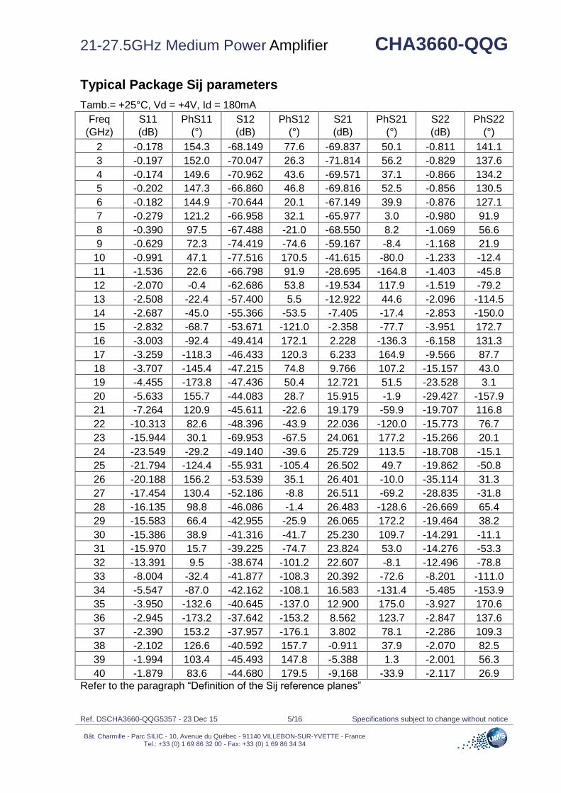
Typical Package Sij parameters
Tamb.= +25°C, Vd = +4V, Id = 180mA
Freq
(GHz)
S11
(dB)
PhS11
(°)
S12
(dB)
PhS12
(°)
S21
(dB)
PhS21
(°)
S22
(dB)
PhS22
(°)
2 -0.178 154.3 -68.149 77.6 -69.837 50.1 -0.811 141.1
3 -0.197 152.0 -70.047 26.3 -71.814 56.2 -0.829 137.6
4 -0.174 149.6 -70.962 43.6 -69.571 37.1 -0.866 134.2
5 -0.202 147.3 -66.860 46.8 -69.816 52.5 -0.856 130.5
6 -0.182 144.9 -70.644 20.1 -67.149 39.9 -0.876 127.1
7 -0.279 121.2 -66.958 32.1 -65.977 3.0 -0.980 91.9
8 -0.390 97.5 -67.488 -21.0 -68.550 8.2 -1.069 56.6
9 -0.629 72.3 -74.419 -74.6 -59.167 -8.4 -1.168 21.9
10 -0.991 47.1 -77.516 170.5 -41.615 -80.0 -1.233 -12.4
11 -1.536 22.6 -66.798 91.9 -28.695 -164.8 -1.403 -45.8
12 -2.070 -0.4 -62.686 53.8 -19.534 117.9 -1.519 -79.2
13 -2.508 -22.4 -57.400 5.5 -12.922 44.6 -2.096 -114.5
14 -2.687 -45.0 -55.366 -53.5 -7.405 -17.4 -2.853 -150.0
15 -2.832 -68.7 -53.671 -121.0 -2.358 -77.7 -3.951 172.7
16 -3.003 -92.4 -49.414 172.1 2.228 -136.3 -6.158 131.3
17 -3.259 -118.3 -46.433 120.3 6.233 164.9 -9.566 87.7
18 -3.707 -145.4 -47.215 74.8 9.766 107.2 -15.157 43.0
19 -4.455 -173.8 -47.436 50.4 12.721 51.5 -23.528 3.1
20 -5.633 155.7 -44.083 28.7 15.915 -1.9 -29.427 -157.9
21 -7.264 120.9 -45.611 -22.6 19.179 -59.9 -19.707 116.8
22 -10.313 82.6 -48.396 -43.9 22.036 -120.0 -15.773 76.7
23 -15.944 30.1 -69.953 -67.5 24.061 177.2 -15.266 20.1
24 -23.549 -29.2 -49.140 -39.6 25.729 113.5 -18.708 -15.1
25 -21.794 -124.4 -55.931 -105.4 26.502 49.7 -19.862 -50.8
26 -20.188 156.2 -53.539 35.1 26.401 -10.0 -35.114 31.3
27 -17.454 130.4 -52.186 -8.8 26.511 -69.2 -28.835 -31.8
28 -16.135 98.8 -46.086 -1.4 26.483 -128.6 -26.669 65.4
29 -15.583 66.4 -42.955 -25.9 26.065 172.2 -19.464 38.2
30 -15.386 38.9 -41.316 -41.7 25.230 109.7 -14.291 -11.1
31 -15.970 15.7 -39.225 -74.7 23.824 53.0 -14.276 -53.3
32 -13.391 9.5 -38.674 -101.2 22.607 -8.1 -12.496 -78.8
33 -8.004 -32.4 -41.877 -108.3 20.392 -72.6 -8.201 -111.0
34 -5.547 -87.0 -42.162 -108.1 16.583 -131.4 -5.485 -153.9
35 -3.950 -132.6 -40.645 -137.0 12.900 175.0 -3.927 170.6
36 -2.945 -173.2 -37.642 -153.2 8.562 123.7 -2.847 137.6
37 -2.390 153.2 -37.957 -176.1 3.802 78.1 -2.286 109.3
38 -2.102 126.6 -40.592 157.7 -0.911 37.9 -2.070 82.5
39 -1.994 103.4 -45.493 147.8 -5.388 1.3 -2.001 56.3
40 -1.879 83.6 -44.680 179.5 -9.168 -33.9 -2.117 26.9
Refer to the paragraph “Definition of the Sij reference planes”
CHA3660-QQG 21-27.5GHz Medium Power Amplifier
Ref. :DSCHA3660-QQG5357 - 23 Dec 15 6/16 Specifications subject to change without notice
Bât. Charmille - Parc SILIC - 10, Avenue du Québec - 91140 VILLEBON-SUR-YVETTE - France
Tel.: +33 (0) 1 69 86 32 00 - Fax: +33 (0) 1 69 86 34 34
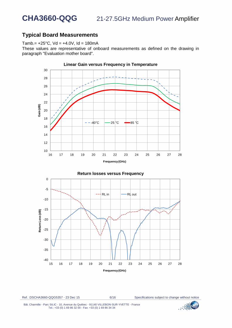
Typical Board Measurements
Tamb.= +25°C, Vd = +4.0V, Id = 180mA
These values are representative of onboard measurements as defined on the drawing in paragraph "Evaluation mother board".
Linear Gain versus Frequency in Temperature
Return losses versus Frequency
10
12
14
16
18
20
22
24
26
28
30
16 17 18 19 20 21 22 23 24 25 26 27 28
Ga
in (d
B)
Frequency (GHz)
-40 C 25 C 85 C
-40
-35
-30
-25
-20
-15
-10
-5
0
15 16 17 18 19 20 21 22 23 24 25 26 27 28
Re
turn
Lo
ss
(d
B)
Frequency (GHz)
RL in RL out

21-27.5GHz Medium Power Amplifier CHA3660-QQG
Ref. DSCHA3660-QQG5357 - 23 Dec 15 7/16 Specifications subject to change without notice
Bât. Charmille - Parc SILIC - 10, Avenue du Québec - 91140 VILLEBON-SUR-YVETTE - France Tel.: +33 (0) 1 69 86 32 00 - Fax: +33 (0) 1 69 86 34 34
Typical Board Measurements
Tamb.= +25°C, Vd = +4.0V, Id = 180mA
Input return loss versus gain ctrl
Output return loss versus gain ctrl
Linear gain & Current versus Gate Voltage
-24
-20
-16
-12
-8
-4
0
16 18 20 22 24 26 28
Input re
turn
loss (dB
)
Frequency (GHz)
Max. Gain
Min. Gain
-32
-28
-24
-20
-16
-12
-8
-4
0
17 18 19 20 21 22 23 24 25 26 27 28 29 30 31
Outp
ut re
turn
loss (dB
)
Frequency (GHz)
Max. Gain
Min. Gain
0
0.05
0.1
0.15
0.2
0.25
0.3
0.35
0
2
4
6
8
10
12
14
16
18
20
22
24
26
28
-1 -0.9 -0.8 -0.7 -0.6 -0.5 -0.4 -0.3
Dra
in c
urr
en
t (A
)
Ga
in (d
B)
Gate voltage (V)
21.2 GHz 24.5 GHz 26.5 GHz Id

CHA3660-QQG 21-27.5GHz Medium Power Amplifier
Ref. :DSCHA3660-QQG5357 - 23 Dec 15 8/16 Specifications subject to change without notice
Bât. Charmille - Parc SILIC - 10, Avenue du Québec - 91140 VILLEBON-SUR-YVETTE - France
Tel.: +33 (0) 1 69 86 32 00 - Fax: +33 (0) 1 69 86 34 34
Typical Board Measurements
Tamb.= +25°C, Vd = +4.0V, Id = 180mA
Noise Figure versus Temperature
Noise Figure & Current versus Gate Voltage
0
1
2
3
4
5
6
7
8
9
10
16 17 18 19 20 21 22 23 24 25 26 27 28 29 30
No
ise
Fig
ure
(d
B)
Frequency (GHz)
85 C 25 C -40 C
0
50
100
150
200
250
300
350
3
4
5
6
7
8
9
10
11
12
13
14
15
16
17
-1 -0.9 -0.8 -0.7 -0.6 -0.5 -0.4 -0.3
Dra
in c
urr
en
t (m
A)
No
ise
fig
ure
(d
B)
Gate voltage (V)
21 GHz 24 GHz 27 GHz Id

21-27.5GHz Medium Power Amplifier CHA3660-QQG
Ref. DSCHA3660-QQG5357 - 23 Dec 15 9/16 Specifications subject to change without notice
Bât. Charmille - Parc SILIC - 10, Avenue du Québec - 91140 VILLEBON-SUR-YVETTE - France Tel.: +33 (0) 1 69 86 32 00 - Fax: +33 (0) 1 69 86 34 34
Typical Board Measurements
Tamb.= +25°C, Vd = +4.0V, Id = 180mA
Output Power & PAE versus Frequency
Pout at 1dB compression versus Temperature
10
12
14
16
18
20
22
24
26
28
30
17 18 19 20 21 22 23 24 25 26 27 28
Ou
tpu
t p
ow
er (
dB
m),
PA
E (%
)
Frequency(GHz)
Psat P-1dB PAE sat
15
16
17
18
19
20
21
22
23
24
25
26
17 18 19 20 21 22 23 24 25 26 27 28
Ou
tpu
t p
ow
er a
t 1
dB
co
mp
. (d
Bm
)
Frequency(GHz)
85°C 25°C -40°C

CHA3660-QQG 21-27.5GHz Medium Power Amplifier
Ref. :DSCHA3660-QQG5357 - 23 Dec 15 10/16 Specifications subject to change without notice
Bât. Charmille - Parc SILIC - 10, Avenue du Québec - 91140 VILLEBON-SUR-YVETTE - France
Tel.: +33 (0) 1 69 86 32 00 - Fax: +33 (0) 1 69 86 34 34
Typical Board Measurements
Tamb.= +25°C, Vd = +4.0V, Id = 180mA
Output TOI versus Output Power DCL
IMD3 versus Output Power DCL
24
26
28
30
32
34
36
38
40
-2 0 2 4 6 8 10 12 14 16 18 20
Ou
tpu
t T
OI (
dB
m)
Output power DCL (dBm)
21.5 GHz 23.5 GHz 24.5 GHz 26.5 GHz 27.5 GHz
20
25
30
35
40
45
50
55
60
65
70
75
80
-2 0 2 4 6 8 10 12 14 16 18 20
IMD
3 (d
Bc
)
Output power DCL (dBm)
21.5 GHz 23.5 GHz 24.5 GHz 26.5 GHz 27.5 GHz

21-27.5GHz Medium Power Amplifier CHA3660-QQG
Ref. DSCHA3660-QQG5357 - 23 Dec 15 11/16 Specifications subject to change without notice
Bât. Charmille - Parc SILIC - 10, Avenue du Québec - 91140 VILLEBON-SUR-YVETTE - France Tel.: +33 (0) 1 69 86 32 00 - Fax: +33 (0) 1 69 86 34 34
Typical Board Measurements
Tamb.= +25°C, Vd = +4.0V, Id = 180mA
IMD3 versus Temperature at 23.5GHz
1-
10
20
30
40
50
60
70
80
90
100
-2 0 2 4 6 8 10 12 14 16 18 20
IMD
3 (d
Bc
)
Output power DCL (dBm)
-40 C 85 C 25 C

CHA3660-QQG 21-27.5GHz Medium Power Amplifier
Ref. :DSCHA3660-QQG5357 - 23 Dec 15 12/16 Specifications subject to change without notice
Bât. Charmille - Parc SILIC - 10, Avenue du Québec - 91140 VILLEBON-SUR-YVETTE - France
Tel.: +33 (0) 1 69 86 32 00 - Fax: +33 (0) 1 69 86 34 34
Package outline (1)
Matte tin, Lead Free (Green) 1- NC 9- Nc
Units : mm 2- Gnd(2) 10- Gnd(2)
From the standard : JEDEC MO-220 3- RF IN 11- RF OUT
(VGGC) 4- Nc 12- Nc
17- GND 5- Gnd(2) 13- Nc
6- VD12 14- VG3
7- VD3 15- Nc
8- Nc 16- VG12
(1) The package outline drawing included to this data-sheet is given for indication. Refer to the application note AN0017 (http://www.ums-gaas.com) for exact package dimensions.
(2) It is strongly recommended to ground all pins marked “Gnd” through the PCB board. Ensure that the PCB board is designed to provide the best possible ground to the package.
21-27.5GHz Medium Power Amplifier CHA3660-QQG
Ref. DSCHA3660-QQG5357 - 23 Dec 15 13/16 Specifications subject to change without notice
Bât. Charmille - Parc SILIC - 10, Avenue du Québec - 91140 VILLEBON-SUR-YVETTE - France Tel.: +33 (0) 1 69 86 32 00 - Fax: +33 (0) 1 69 86 34 34
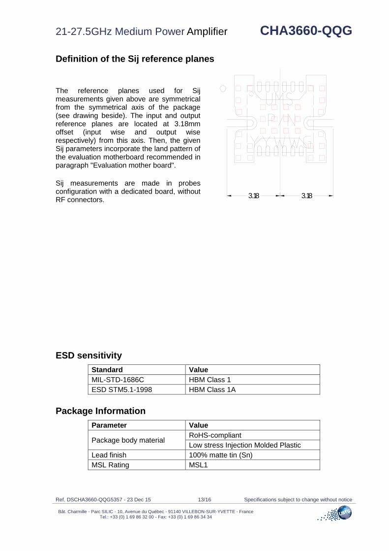
Definition of the Sij reference planes
The reference planes used for Sij measurements given above are symmetrical from the symmetrical axis of the package (see drawing beside). The input and output reference planes are located at 3.18mm offset (input wise and output wise respectively) from this axis. Then, the given Sij parameters incorporate the land pattern of the evaluation motherboard recommended in paragraph "Evaluation mother board".
Sij measurements are made in probes configuration with a dedicated board, without RF connectors.
ESD sensitivity
Standard Value
MIL-STD-1686C HBM Class 1
ESD STM5.1-1998 HBM Class 1A
Package Information
Parameter Value
Package body material
RoHS-compliant
Low stress Injection Molded Plastic
Lead finish 100% matte tin (Sn)
MSL Rating MSL1
3.18 3.18

CHA3660-QQG 21-27.5GHz Medium Power Amplifier
Ref. :DSCHA3660-QQG5357 - 23 Dec 15 14/16 Specifications subject to change without notice
Bât. Charmille - Parc SILIC - 10, Avenue du Québec - 91140 VILLEBON-SUR-YVETTE - France
Tel.: +33 (0) 1 69 86 32 00 - Fax: +33 (0) 1 69 86 34 34
Evaluation mother board
Compatible with the proposed footprint.
Based on typically Ro4350 / 10mils or equivalent.
Using a micro-strip to coplanar transition to access the package.
Recommended for the implementation of this product on a module board.
Decoupling capacitors of 100pF ±5% and 10nF ±10% are recommended for all DC accesses.
See application note AN0017 for details.

21-27.5GHz Medium Power Amplifier CHA3660-QQG
Ref. DSCHA3660-QQG5357 - 23 Dec 15 15/16 Specifications subject to change without notice
Bât. Charmille - Parc SILIC - 10, Avenue du Québec - 91140 VILLEBON-SUR-YVETTE - France Tel.: +33 (0) 1 69 86 32 00 - Fax: +33 (0) 1 69 86 34 34
Notes
Due to ESD protection circuits on RF input and output, an external capacitance might be requested to isolate the product from external voltage that could be present on the RF accesses.
ESD protections are also implemented on all DC accesses.
The DC connections do not include any decoupling capacitor in package, therefore it is mandatory to provide a good external DC decoupling on the PC board, as close as possible to the package.
DC Schematic
4V, 180mA
465 Ω 465 Ω 465 Ω
IN
OUT
G12
33mA
25 Ω 20 Ω 6 Ω
D12
63mA
D3
84mA
G3
x1 x7
x3x1 x3x1 x3x1
x1 x7 x1 x7

CHA3660-QQG 21-27.5GHz Medium Power Amplifier
Ref. :DSCHA3660-QQG5357 - 23 Dec 15 16/16 Specifications subject to change without notice
Bât. Charmille - Parc SILIC - 10, Avenue du Québec - 91140 VILLEBON-SUR-YVETTE - France
Tel.: +33 (0) 1 69 86 32 00 - Fax: +33 (0) 1 69 86 34 34
Recommended package footprint
Refer to the application note AN0017 available at http://www.ums-gaas.com for package foot print recommendations.
SMD mounting procedure
For the mounting process standard techniques involving solder paste and a suitable reflow process can be used. For further details, see application note AN0017.
Recommended environmental management
UMS products are compliant with the regulation in particular with the directives RoHS N°2011/65 and REACh N°1907/2006. More environmental data are available in the application note AN0019 also available at http://www.ums-gaas.com.
Recommended ESD management
Refer to the application note AN0020 available at http://www.ums-gaas.com for ESD sensitivity and handling recommendations for the UMS package products.
Ordering Information
QFN 4x4 package: CHA3660-QQG/XY
Stick: XY = 20 Tape & reel: XY = 21
Information furnished is believed to be accurate and reliable. However United Monolithic Semiconductors S.A.S. assumes no responsibility for the consequences of use of such information nor for any infringement of
patents or other rights of third parties which may result from its use. No license is granted by implication or otherwise under any patent or patent rights of United Monolithic Semiconductors S.A.S.. Specifications
mentioned in this publication are subject to change without notice. This publication supersedes and replaces all information previously supplied. United Monolithic Semiconductors S.A.S. products are not authorised for use as critical components in life support devices or systems without express written approval from United Monolithic Semiconductors S.A.S.


