
DIGITAL VIDEO CAMCORDERChassis : Dragon IIIBASIC : VP-D371Application Models : VP-D371(i), VP-D371W(i),
VP-D372WH(i),VP-D374 VP-D375W(i),VP-D376VP-D975W(i)
Application Area: XEF, XEU, XEG, XET, XEV, XEC, XSA, CDM,
XST, XEO, XEH, XEP, XEE, EAP, EUR, XEN, HACO, TAW, TIT, COL, SEO, XSS, SED, XSH, XSG, FES, XTL, CHN, ZAM, STS, SMR, XFA, ITN, KNT, XSE, FPT, RAD, AFR, AND, UMGMEA, SEA
SERVICE ΠShooting & compact Design
´ Direct Print System : PictBridgeTM
ˇ LED Light
¨ High quality MPEG4
ˆ Still image Interpolation
Ø Real Wide mode (16:9)/WIDE LCD
∏ 34X ZOOM (Normal model)
26X ZOOM (Mega model)
” USB 2.0 Streaming
Manual
DIGITAL VIDEO CAMCORDER Merit & Character regarding Product
SERVICE MA
NU
AL
VP-D371(i)/D
371W(i)/D
372WH
(i)/D374/D
375W(i)/D
376/D975W
(i)
ELECTRONICS
© Samsung Electronics Co., Ltd. FEB. 2007Printed in KoreaAD82-00183A
This Service Manual is a property of Samsung Electronics Co .,Ltd.Any unauthorized use of Manual can be punished under applicable
International and/or domestic law.
Area Web SiteNorth America URL ; http://service.samsungportal.com
Latin America URL ; http://latin.samsungportal.com
CIS URL ; http://cis.samsungportal.com
Europe URL ; http://europe.samsungportal.com
China URL ; http://china.samsungportal.com
Asia URL ; http://asia.samsungportal.com
Mideast & Africa URL ; http://mea.samsungportal.com
◆ If you want to know additional information which is not included on thisService Manual, Please refer to the SKP(Samsung Knowledge Portal)web site.

Block Diagrams
7-2 Samsung ElectronicsThis Document can not be used without Samsung’s authorization
DC/DC BLOCK
AUDIO VIDEO I/FBLOCK
Syscon/Servo Block
PRML/PRE-Amp BlockDV1 chip Block
5V3.3V1.8V
BL5V-15V~-7.5V
Drum VSCapstan VS
7-1 All Block Diagram

Block Diagrams
Samsung Electronics 7-3This Document can not be used without Samsung’s authorization
S5C7377XADC 2CH(500KHz10Bits)
ARM926NANDFLASHCONTROLLER
SDRAMC/SMC
APBBRIDGE
SPIAUDIO CODEC(G. 728/G/711)
I2S
I2C *2
UART *2
GPIO
INTC
TIMER *4
WDT
USB 2.0
MSPROSDIO/MMC
DMA *4VIDEO DMAJPEGCODEC
MPEG4CODEC(30FPS@VGA)
OSD
AHB BUS
CCD[11:0]Y/Cb/Cr[7:0]
CCD[11:0]Y/Cb/Cr[7:0]
VIDEO BUSY/C CHANNEL
CAMERA
PROCESSORDIS
ImageimprovementProcessor
MotorControl
PWM(12CH)
Y/Cb/Cr[9:0]Y/C[7:0]
Y[9:0]
APB
BUS
Key
CCD12bits
TV Encoder Itur656
S5C7376X
ExternalDevice
ExternalDeviceExternalDevice
Console
S/Wusage
PC
3-in-1CARDSocket
Nand FlashMemory
ExternalMemory
7-2 ICD01(S5C7377X) Block Diagram

Block Diagrams
7-4 Samsung ElectronicsThis Document can not be used without Samsung’s authorization
SHUFFLEVIDEO CODEC
AUDIO
AUXSC
DVC_LINK
IIC
CODEC(channel)
MODAS
DEMOD
VCO
DAC4MBits
SDRAM10.5MBitsSDRAM
1394PHY
MICOM
Camera
PRML
AudioAD/DA
VideoDecoder
CLOCK
OSD
2nd-DV1CHIP
LCD
AFE
AudiooDSP
ColorEncoderr
7-3 IC201 Block Diagram

Block Diagrams
Samsung Electronics 7-5This Document can not be used without Samsung’s authorization
DCDCBLOCK
PRMLBLCOK
PREAMPBLOCK
DV1_CHIPBLOCK
AV I/FBLOCK
CAMERABLOCK
TMP1962F10(IC501)
MICOM
LB11993W(IC401)
MOTORDIRVER
DRUMMOTOR
CAPMOTOR
LOAGDINGMOTOR
T/S SENSORREEL SENSORMIC SENSORRS5C372A
(IC502)RTC IC
EEPROM524ABOX91(IC505)
RESET-ICXC6413FY01MR(IC503)
7-4 Syscon/Servo Block Diagram
LPF
LPF
LPF
LPF
LPF
LPF
LPF
LPF
BATT &ADAPTER
TMP1962(IC501)MICOM
VTR DD ON
CAM DD ON
LPF
LPF
BD983KV(IC701)
PWM-IC
D.ERR
C.ERR
DRUM VS
CAPSTAN VS
SS 3.0V
SS 5.0V
SS 1.8V
LCD BL5V
CCD/LCD-7.5V, -5V, -5V
V.LOGHT5.0V
7-5 DC/DC Block Diagram

Samsung Electronics 8-1
8. Wiring Diagram

Schematic Diagrams
10-2 Samsung ElectronicsThis Document can not be used without Samsung’s authorization
10-1 DC/DC (Main PCB)
ΠQ701
´ Q702
ˇ Q703
¨ Q706
ˆ Q707
Ø Q708
◆ These are the waveforms of VP-D371(i)/D371W(i)/D372WH(i)/D375W(i)/D975W(i)Caution) There can be some differences (Voltage, Frequency, stc.) among cameras.

Schematic Diagrams
Samsung Electronics 10-3This Document can not be used without Samsung’s authorization
10-2 Micom (Main PCB)
◆ These are the waveforms of VP-D371(i)/D371W(i)/D372WH(i)/D375W(i)/D975W(i)Caution) There can be some differences (Voltage, Frequency, stc.) among cameras.
ΠX501(13.5MHz)

Schematic Diagrams
10-4 Samsung ElectronicsThis Document can not be used without Samsung’s authorization
10-3 Servo (Main PCB)
Œ IC401-25Pin(VCC1) ´ IC401-23Pin ˇ IC401-28Pin ¨ IC401-44Pin(Cap VS) ˆ IC401-51Pin(Cap W)) Ø IC401-52Pin(Cap V) ∏ IC401-54Pin(Cap U)
◆ These are the waveforms of VP-D371(i)/D371W(i)/D372WH(i)/D375W(i)/D975W(i)Caution) There can be some differences(Voltage, Frequency, stc.) among cam-eras.

Schematic Diagrams
Samsung Electronics 10-5This Document can not be used without Samsung’s authorization
Audio
10-4 Audio (Main PCB)
´ IC601 64Pin(Audio LR CLK)Œ IC601 53, 57Pin
◆ These are the waveforms of VP-D371(i)/D371W(i)/D372WH(i)/D375W(i)/D975W(i)Caution) There can be some differences (Voltage, Frequency, stc.) among cameras.

Schematic Diagrams
10-6 Samsung ElectronicsThis Document can not be used without Samsung’s authorization
10-5 CDS (Main PCB)

Schematic Diagrams
Samsung Electronics 10-7This Document can not be used without Samsung’s authorization
VideoAudio
10-6 Camera DSP (Main PCB)
Schematic Diagrams
10-8 Samsung ElectronicsThis Document can not be used without Samsung’s authorization
VideoAudio
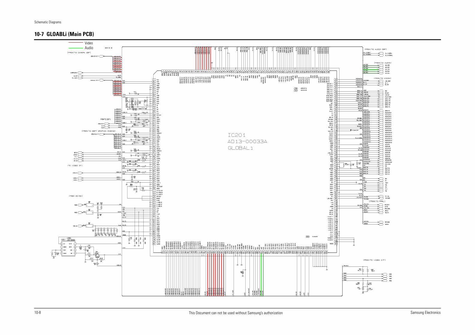
10-7 GLOABLi (Main PCB)

Schematic Diagrams
Samsung Electronics 10-9This Document can not be used without Samsung’s authorization
Video
10-8 LCD, CVF (Main PCB)

Schematic Diagrams
10-10 Samsung ElectronicsThis Document can not be used without Samsung’s authorization
10-9 Memory (Main PCB)

Schematic Diagrams
Samsung Electronics 10-11This Document can not be used without Samsung’s authorization
10-10 PLL (Main PCB)

Schematic Diagrams
10-12 Samsung ElectronicsThis Document can not be used without Samsung’s authorization
10-11 PRML (Main PCB)

Schematic Diagrams
Samsung Electronics 10-13This Document can not be used without Samsung’s authorization
10-12 Vertical Drive (Main PCB)

Schematic Diagrams
10-14 Samsung ElectronicsThis Document can not be used without Samsung’s authorization
10-13 Zoom motor Drive (Main PCB)

Schematic Diagrams
Samsung Electronics 10-15This Document can not be used without Samsung’s authorization
10-14 2.5” LCD (LCD PCB (VP-D371(i)))

Schematic Diagrams
10-16 Samsung ElectronicsThis Document can not be used without Samsung’s authorization
10-15 2.7” LCD (LCD PCB (VP-D371W(i)/D372WH(i)/D375W(i)/D975W(i)))

Schematic Diagrams
Samsung Electronics 10-17This Document can not be used without Samsung’s authorization
10-16 CCD Normal (CCD PCB (VP-D371(i)/D371W(i)/D372WH(i)/D375W(i)))

Schematic Diagrams
10-18 Samsung ElectronicsThis Document can not be used without Samsung’s authorization
10-17 CCD Mega (CCD PCB (VP-D975W(i)))

Schematic Diagrams
Samsung Electronics 10-19This Document can not be used without Samsung’s authorization
10-18 Jack (Jack PCB)

Schematic Diagrams
10-20 Samsung ElectronicsThis Document can not be used without Samsung’s authorization
10-19 Rear (Rear PCB)

Schematic Diagrams
Samsung Electronics 10-21This Document can not be used without Samsung’s authorization
10-20 Function (Function PCB)

Schematic Diagrams
10-22 Samsung ElectronicsThis Document can not be used without Samsung’s authorization
10-21 CVF (CVF PCB)

Schematic Diagrams
Samsung Electronics 10-23This Document can not be used without Samsung’s authorization
10-22 Front (Front PCB (VP-D372WH(i)/D375W(i)/D975W(i)))


