IOSR Journal of Electrical and Electronics Engineering (IOSR-JEEE)
e-ISSN: 2278-1676,p-ISSN: 2320-3331, Volume 11, Issue 4 Ver. I (Jul. – Aug. 2016), PP 98-108
www.iosrjournals.org
DOI: 10.9790/1676-11040198108 www.iosrjournals.org 98 | Page
Designing and simulation of low and rapid voltage comparator
Nima Eivaz Ziaei [email protected]
Electricity-Electronic Department, Azad University branch of Tabriz, Tabriz, Iran
Abstract: Dynamic comparators are used widely in lots of circuits and systems. They have a high speed
performance with positive feedback structure. Analog to digital convertors, regulator switches, memories and
processors can be mentioned as their applications.Important parameters that are considerable in dynamic
comparators are offset voltage, lag time and the speed of comparator.In this article the offset voltage, the
compare speed and the lag time of two popular comparator, Strong Arm and Double Thiel, have been surveyed.
Finally a rapid and low voltage comparator has been designed. For designed comparator in Vcm=1(mV) and
VDD=1.2 (V) circumstances the lag time and offset voltage have been obtained equal to 162(ps) and 3.65 (mV)
respectively. The parameters of dynamic comparators were simulated and surveyed by the Cadence Virtuoso XL
and Hspice software in nmCMOS 180 technology.
Keywords: offset voltage, kickback noise voltage, lag time, velocity
I. Introduction
Nowadays,along with the electronic science advancement, some circuits are needed to make
relationship between the analog and digital world in digital domain. Achieving this aim, therefore, the more
comparators are needed.Demand for the low energy consumption, small area for the electronic chipsets and high
speed analog-digital convertor, caused the using of dynamic comparator rising, achieving the high speed and
low energy consumption.
In this article the lag time of comparators has been assessed, using the analytical analysis.The designers
and engineers can determine the effective parameters on lag time and other parameters in comparator
performance, using the analytic analysis. A novel comparator in addition to analytic analysis has been designed
with an innovative architecture and its performance has been compared with Strong Arm and Double Tail
comparators. The comparators are circuits that can recognize the magnitude or the exiguity of signals from the
zero reference, maximum or minimum amounts (Tony Chan Carusone , et .al ,2012).Meanwhile, increasing the
sensitive and portable sensors in strategic professions such as medicine, biochemistry and etcetera show the
necessity of low voltage, rapid and small comparator existence (Yongfu Li,et .al,2014 and Teknol. Mara,et.al
,2011).
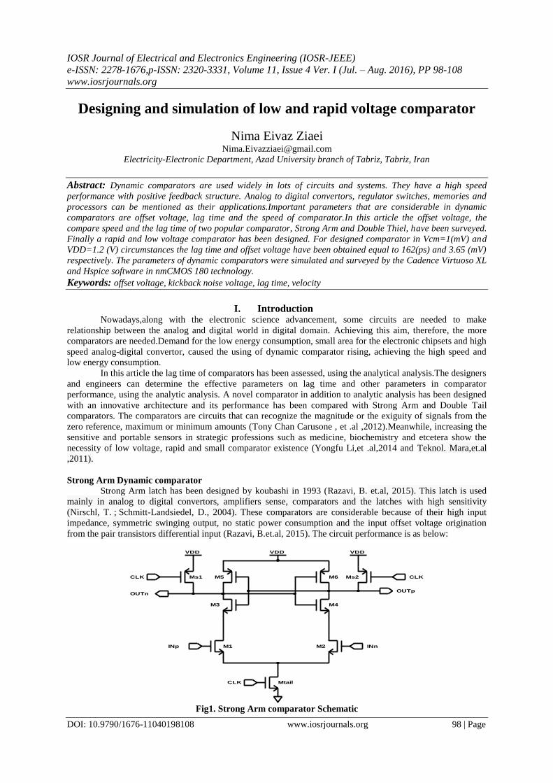
Strong Arm Dynamic comparator Strong Arm latch has been designed by koubashi in 1993 (Razavi, B. et.al, 2015). This latch is used
mainly in analog to digital convertors, amplifiers sense, comparators and the latches with high sensitivity
(Nirschl, T. ; Schmitt-Landsiedel, D., 2004). These comparators are considerable because of their high input
impedance, symmetric swinging output, no static power consumption and the input offset voltage origination
from the pair transistors differential input (Razavi, B.et.al, 2015). The circuit performance is as below:
Fig1. Strong Arm comparator Schematic
INp INn
CLK
VDD
M1
Mtail
M3
M2
M4
M6M5
OUTpOUTn
Ms1 Ms2CLK CLK
VDD VDD
Designing and simulation of low and rapid voltage comparator
DOI: 10.9790/1676-11040198108 www.iosrjournals.org 99 | Page
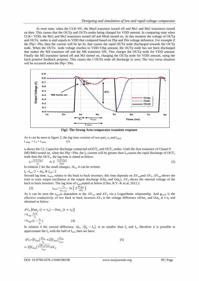
At reset state, when the CLK=0V, the Mtail transistor turned off and Ms1 and Ms2 transistors turned
on then. This causes that the OUTp and OUTn nodes being charged for VDD amount. In comparing state when
CLK= VDD, the Ms1 and Ms2 transistors turned off and Mtail turned on. At this moment the voltage of OUTp
and OUTn nodes is stail equals to VDD that compared based on INp and INn voltage deference. For example if
the INp> INn, then the current will be Ip>In, that causes the rapid OUTn node discharged towards the OUTp
node. When the OUTn node voltage reaches to VDD-Vthp amount, the OUTp node has not been discharged
that makes the M4 transistor off and the M6 transistor ON. This charges the OUTp node for VDD amount.
Finally the M5 transistor turned off and M3 turned on, charging the OUTp node for VDD amount, using the
latch positive feedback property. This causes the f OUTn node ull discharge to zero; The vice versa situation
will be occurred when the INp< INn.
Fig2. The Strong Arm comparator transient response
As it can be seen in figure 2, the lag time consists of two part, t0 and tlatch
(1) t delay = t 0 + t latch
t0 shows the CL Capacitor discharge connected toOUTp and OUTn nodes. Until the first transistor of Chanel P
(M5/M6) turned on, when the INp >INn, the Ip current will be greater than In,causes the rapid discharge of OUTn
node than the OUTp. the lag time is stated as below:
(2) 𝐶𝐿 𝑉𝑡𝑝
𝐼𝑡𝑎𝑖𝑙 ≅ 2 tₒ=
CL 𝑉𝑡𝑝
𝐼𝑝
In relation 2 for the small changes, ∆Iin, it can be written:
Ip =Itail /2 + ∆Iin Itail / 2
Second lag time, tlatch, relates to the back to back inverters; this time depends on ∆Voutand ∆V0. ∆Vout shows the
train to train output oscillation at the output discharge (Outn and Outp). ∆V0 shows the internal voltage of the
back to back inverters. The lag time of tlatchstated as below (Choi, R.Y.-K et.al, 2012.):
(3) tlatch =𝐶𝐿
𝑔𝑚 ,𝑒𝑓𝑓 ln 2
∆𝑉𝑂𝑢𝑡
∆𝑉0
As it can be seen the tlatchis dependent to the ∆Vout and ∆V0 via a Logarithmic relationship. And gm.eff is the
effective conductivity of two back to back inverters.∆V0 is the voltage difference ofOutn and Outp at t=t0 and
obtained as below:
∆V0= Out𝑝 𝑡 = 𝑡0 − 𝑂𝑢𝑡𝑛 (𝑡 = 𝑡0)
=Vthp -𝐼𝑛 𝑡0
𝐶𝐿
(4)=Vthp (1 −𝐼𝑛
𝐼𝑝 )
In relation 4 the current difference, ∆Iin = 𝐼𝑝 − 𝐼𝑛 , is so smaller than Ip and In, therefore it is possible to
approximate the Ip with the half of Itail, then we have:
∆V0= 𝑉𝑡𝑝 ∆𝐼𝑖𝑛
𝐼𝑝≈2 𝑉𝑡𝑝
∆𝐼𝑖𝑛
𝐼𝑡𝑎𝑖𝑙 (5)
= 2 𝑉𝑡𝑝 2𝛽1,2𝐼𝑡𝑎𝑖𝑙
𝐼𝑡𝑎𝑖𝑙∆Vin
Designing and simulation of low and rapid voltage comparator
DOI: 10.9790/1676-11040198108 www.iosrjournals.org 100 | Page
=2 𝑉𝑡𝑝 2𝛽1,2
𝐼𝑡𝑎𝑖𝑙 ∆Vin (6)
𝛃1,2 is the conductivity coefficient of M1 and M2 transistors. Substituting the 3 and 6 relations we have:
t latch =𝐶𝐿
𝑔𝑚 ,𝑒𝑓𝑓ln
∆𝑉𝑂𝑢𝑡 𝐼𝑡𝑎𝑖𝑙
∆𝑉𝑖𝑛 2𝛽1,2 𝑉𝑡𝑝 (7 )
The output voltage oscillation,∆VOut = VDD/2 gained from the internal voltage difference ∆V0 at the output
voltage drop (Outp and Outn). Therefore the half of voltage resource considered the threshold inverter or SR
latch (Babayan-Mashhadi, 2013). Substituting the relations 1, 2 and 7 we have:
(8 )tdelay= 2𝐶𝐿 𝑉𝑡𝑝
𝐼𝑡𝑎𝑖𝑙+
𝐶𝐿
𝑔𝑚 ,𝑒𝑓𝑓ln
𝑉𝐷𝐷 𝐼𝑡𝑎𝑖𝑙
2 ∆𝑉𝑖𝑛 2𝛽1,2 𝑉𝑡𝑝
As it can be seen in relation 8, the lag time dependence on some factors. The lag time has a direct relation to the
load capacitor (CL). The effect of Itail is obvious in t0 and tlatch it has an inverse relation to t0 and a direct relation
to tlatch and𝐼𝑡𝑎𝑖𝑙1
2 . Generally the lag time is reduced with increasing in Itail. Also the effect of ∆Vin and ∆Vout is
obvious in tlatch.Vin voltage has an indirect relation to the lag time, when the Vin increases the Itail will increase
and the internal voltage decreases subsequently. Unit current tail of this comparator is the negative property.
Tail current decreasing causes the Ip and In reduction subsequently (Itail = Ip + In) and it rises the lag time. For the
lag time reduction it is better to increase the Itail (D. Shinkelet. al, 2007).
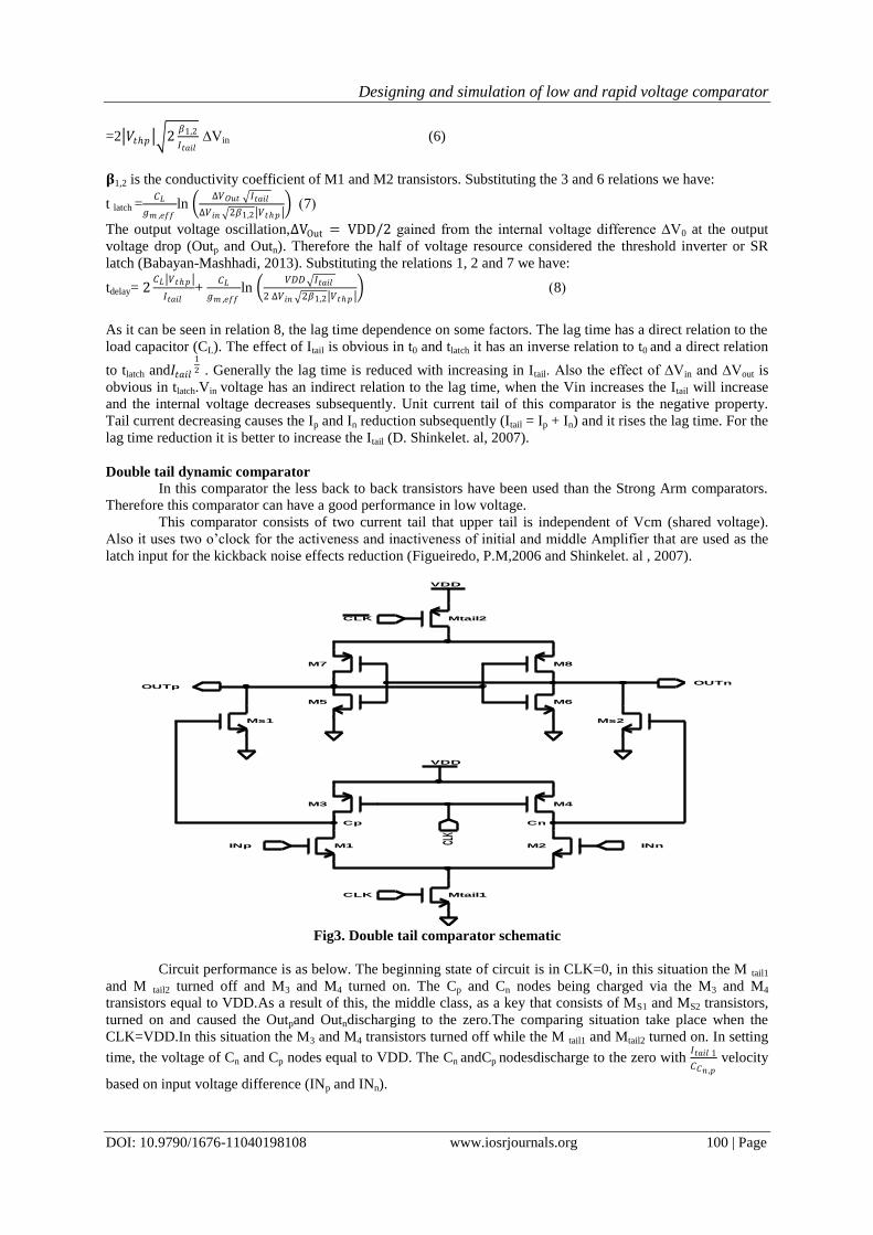
Double tail dynamic comparator In this comparator the less back to back transistors have been used than the Strong Arm comparators.
Therefore this comparator can have a good performance in low voltage.
This comparator consists of two current tail that upper tail is independent of Vcm (shared voltage).
Also it uses two o’clock for the activeness and inactiveness of initial and middle Amplifier that are used as the
latch input for the kickback noise effects reduction (Figueiredo, P.M,2006 and Shinkelet. al , 2007).
Fig3. Double tail comparator schematic
Circuit performance is as below. The beginning state of circuit is in CLK=0, in this situation the M tail1
and M tail2 turned off and M3 and M4 turned on. The Cp and Cn nodes being charged via the M3 and M4
transistors equal to VDD.As a result of this, the middle class, as a key that consists of MS1 and MS2 transistors,
turned on and caused the Outpand Outndischarging to the zero.The comparing situation take place when the
CLK=VDD.In this situation the M3 and M4 transistors turned off while the M tail1 and Mtail2 turned on. In setting
time, the voltage of Cn and Cp nodes equal to VDD. The Cn andCp nodesdischarge to the zero with 𝐼𝑡𝑎𝑖𝑙 1
𝐶𝐶𝑛 ,𝑝
velocity
based on input voltage difference (INp and INn).
INp INn
CLK
CLK
VDD
M1
Mtail1
M5
M2
Mtail2
M6
M8M7
OUTnOUTp
M3 M4
VDD
Ms1 Ms2
CLK
Cp Cn

Designing and simulation of low and rapid voltage comparator
DOI: 10.9790/1676-11040198108 www.iosrjournals.org 101 | Page
Fig4. Transient response of double tail comparator
In this comparator the lag time based on relation 2 consists of two part. First part relates to the capacitor
discharging (CL1,2), connected to Outp,n until the first voltage of n-channel transistor reaches to the Vthn to turn
on (t0).Therefore the t0 obtained as below:
(9)2𝑉𝑡𝑛𝐶𝐿 𝑜𝑢𝑡
𝐼𝑡𝑎𝑖𝑙 2= t0 =
𝑉𝑡𝑛𝐶𝐿 𝑜𝑢𝑡
𝐼𝐷1
ID1 current in this transistor considered as M6. When the first n-channel transistor turned on, the Outnnode
voltage discharged to the zero, then the M5 transistor turned off and M7 turned on, caused the Outp node
charging to the VDD amount. The lag time of latch obtained from relation 3. Calculating the internal voltage
difference of ∆V0 at t0 is as below:
∆V0= Out𝑝 𝑡 = 𝑡0 − 𝑂𝑢𝑡𝑛 (𝑡 = 𝑡0)
=Vthn - 𝐼𝐷2𝑡0
𝐶𝐿 𝑜𝑢𝑡
(10) = Vthn 1 −𝐼𝐷2
𝐼𝐷1
In upper relation the current difference, ∆Iin = 𝐼𝐷1 − 𝐼𝐷2 , is so lesser than ID1 and ID2.Therefore the ID1 can be
approximated by the half of Itail2 current. Then it can be written:
(11) = 𝑔𝑚𝑆1,2∆𝑉𝑐𝑝/𝑐𝑛 Ilatch = 𝐼𝐷1 − 𝐼𝐷2 ∆
Having the relation 10 and 11:
2Vthn
∆𝐼𝑙𝑎𝑡𝑐
𝐼𝑡𝑎𝑖𝑙 2 ≈ V0 = Vthn
∆𝐼𝑙𝑎𝑡𝑐
𝐼𝐷1∆
(12) ∆Vcp/cn =2Vthn
𝑔𝑚𝑠 1,2
𝐼𝑡𝑎𝑖𝑙 2
As it can be seen in relation 12, the internal voltage difference (∆V0) at the moment t0 is dependent on
conductivity coefficient of Ms1 and Ms2 transistors and the output voltage difference of first class.The output
voltage difference of first class obtained as below:
∆Vcp/cn = V𝑐𝑝 𝑡 = 𝑡0 − 𝑉𝑐𝑛 (𝑡 = 𝑡0)
= t0
𝐼𝑝−𝐼𝑛
𝐶𝐿 𝑐𝑝 ,𝑛
(13) =t0
𝑔𝑚1,2∆𝑉𝑖𝑛
𝐶𝐿 𝑐𝑝 ,𝑛
In these relations the Ip and In relates to the M1 and M2 transistor currents that discharge the Cp and Cn nodes.
(14) ∆Iin=gm1,2∆Vin
From the relations 12, 13 and 14 we have:
(15) 𝑔𝑚𝑠1,2𝑔𝑚1,2∆𝑉𝑖𝑛 𝐶𝐿 𝑂𝑢𝑡
𝐶𝐿𝑐𝑝 ,𝑛 2
𝑉𝑡𝑛
𝐼𝑡𝑎𝑖𝑙 2
2
∆V0 =
The internal voltage difference of latch at t0 moment, depends on input conductivity coefficient of
middle class and the capacitor ratio ofCL Out , CLcp ,n andItail 2. The output voltage oscillation, ∆Vout=VDD/2,
obtained from the internal voltage, ∆V0, at the output voltage drop. Therefore the half of voltage resource
considered as the threshold inverter or the SR latch (Babayan-Mashhadi, 2013). The lag time obtained from the
relations 1, 9 and 15.
t delay = t 0 + t latch
Designing and simulation of low and rapid voltage comparator
DOI: 10.9790/1676-11040198108 www.iosrjournals.org 102 | Page
= 2𝑉𝑡𝑛𝐶𝐿 𝑂𝑢𝑡
𝐼𝑡𝑎𝑖𝑙 2+
𝐶𝑙 𝑂𝑢𝑡
𝑔𝑚 ,𝑒𝑓𝑓Ln
∆𝑉𝑂𝑢𝑡
∆𝑉0
=2 𝑉𝑡𝑛𝐶𝐿 𝑂𝑢𝑡
𝐼𝑡𝑎𝑖𝑙 2 +
𝐶𝐿 𝑂𝑢𝑡
𝑔𝑚 ,𝑒𝑓𝑓 Ln
𝑉𝐷𝐷 .𝐶𝐿𝑐𝑝 ,𝑛 .𝐼𝑡𝑎𝑖𝑙 22
𝐶𝐿 𝑂𝑢𝑡 .𝑔𝑚𝑆 1.2𝑔𝑚1,2∆𝑉𝑖𝑛 4𝑉𝑡𝑛2 (16)
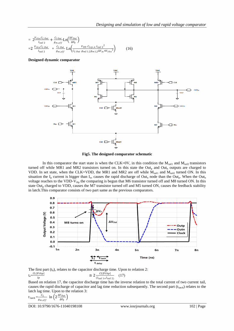
Designed dynamic comparator
Fig5. The designed comparator schematic
In this comparator the start state is when the CLK=0V, in this condition the Mtail1 and Mtail2 transistors
turned off while MR1 and MR2 transistors turned on. In this state the Outp and Outn outputs are charged to
VDD. In set state, when the CLK=VDD, the MR1 and MR2 are off while Mtail1 and Mtail2 turned ON. In this
situation the Ip current is bigger than In, causes the rapid discharge of Outn node than the Outp. When the Outn
voltage reaches to the VDD-Vthp the comparing is begun that M6 transistor turned off and M8 turned ON. In this
state Outp charged to VDD, causes the M7 transistor turned off and M5 turned ON, causes the feedback stability
in latch.This comparator consists of two part same as the previous comparators.
The first part (t0), relates to the capacitor discharge time. Upon to relation 2:
(17) ≅ 2𝐶𝐿 𝑉𝑡𝑝
(𝐼𝑡𝑎𝑖𝑙 1+𝐼𝑡𝑎𝑖𝑙 2) tₒ=
CL 𝑉𝑡𝑝
𝐼𝑝
Based on relation 17, the capacitor discharge time has the inverse relation to the total current of two current tail,
causes the rapid discharge of capacitor and lag time reduction subsequently. The second part (tlatch) relates to the
latch lag time. Upon to the relation 3:
t latch =𝐶𝐿
𝑔𝑚 ,𝑒𝑓𝑓 ln 2
∆𝑉𝑂𝑢𝑡
∆𝑉0

Designing and simulation of low and rapid voltage comparator
DOI: 10.9790/1676-11040198108 www.iosrjournals.org 103 | Page
∆V0= Out𝑝 𝑡 = 𝑡0 − 𝑂𝑢𝑡𝑛 (𝑡 = 𝑡0)
=Vthp -𝐼𝑛 𝑡0
𝐶𝐿
=Vthp (1 −𝐼𝑛
𝐼𝑝 )
) Vthp (∆𝐼𝑖𝑛
𝐼𝑝 =
In upper relation the current difference, ∆Iin = 𝐼𝑝 − 𝐼𝑛 , is very smaller than Ip and In; therefore the Ip can be
approximated by the half of Itail1+Itail2 current. Therefore it can be written:
(18) ) ∆V0=2. Vthp(∆𝐼𝑖𝑛
(𝐼𝑡𝑎𝑖𝑙 1+𝐼𝑡𝑎𝑖𝑙 2)
From the relation 11 and 18:
(19) ) 𝑔𝑚1,2∆𝑖𝑛
(𝐼𝑡𝑎𝑖𝑙 1+𝐼𝑡𝑎𝑖𝑙 2) ∆V0 =2.Vthp (
From the relation 3 and 19:
(20) tlatch = 𝐶𝐿
𝑔𝑚 ,𝑒𝑓𝑓.ln(
(𝐼𝑡𝑎𝑖𝑙 1+𝐼𝑡𝑎𝑖𝑙 2)∆𝑉𝑂𝑢𝑡
𝑉𝑡𝑝𝑔𝑚 1,2∆𝑉𝑖𝑛)
As it can be seen in relation 20, the latch lag time has a direct relation to the total current of tail 1 and 2,
also it has an inverse relation to M1 and M2 transistors.In this relation the tail 1 current is dependent on input
voltage while the tail 2 current is a constant current resource that active and inactive by a clock. The output
voltage oscillation, ∆Vout=VDD/2, obtained from the internal voltage, ∆V0, difference at the output voltage
drop.So, the half of voltage resource considered as the threshold inverter voltage or SR latch (Babayan and
Mashhadi, 2013). We have from 1, 17 and 20:
t delay = t 0 + t latch
(21) ) .ln(𝑉𝐷𝐷 𝐼𝑡𝑎𝑖𝑙 1+𝐼𝑡𝑎𝑖𝑙 2
2𝑉𝑡𝑝𝑔𝑚1,2∆𝑉𝑖𝑛 tdelay =
2𝐶𝐿 𝑉𝑡𝑝
𝐼𝑡𝑎𝑖𝑙 1+𝐼𝑡𝑎𝑖𝑙 2 +
𝐶𝐿
𝑔𝑚 ,𝑒𝑓𝑓
As it is obvious in relation 21, the lag time has been reduced than two aforementioned relations, that simulation
results approves it.
The comparator’s kickback noise Basically in comparator circuits, the huge voltage changes in latch nodes is coupled via the para static
capacitors of transistor to the comparator circuit entrance. This operation causes the input voltage confusion in
comparator and the error in its performance. This error in comparators, is called kickback noise (Figueiredo,
P.M et.al, 2006 and Babayan-Mashhadi, 2013).The Strong Arm and the designed comparators have the higher
kickback noise error, because they are not isolated from the latch comparator, while the double tail comparator
has the small kickback noise because it is isolated from the latch comparator.
Fig7. The kickback noise range versus the input voltage domain
Offset voltage of comparators
Offset voltage is the difference of input DC voltage consists of a comparator, APMP and amplifier.
Offset voltage in low voltage comparator causes the logical level and undesirable behavior in digital circuit
output, subsequently it causes the incorrect performance of comparators and the higher energy consumption.
0
50
100
150
200
1m 10m 100m 950m
Pea
k In
pu
t V
olt
age
Erro
r (m
V)
Input Amplitude (mV)
Strong Arm Comparator Double-tail Comparator
Proposed Comparator

Designing and simulation of low and rapid voltage comparator
DOI: 10.9790/1676-11040198108 www.iosrjournals.org 104 | Page
Therefore the offset voltage should be studied and evaluated in very sensitive applications. The comparators
have been optimized in this study and the transistor’s parameters have been considered that an offset standard
deviation is equal to 4(mV) with the shared input voltage equal to 1.1(V) (Babayan-Mashhadi, 2013 and D.
Shinkelet. al, 2007).
Fig8. The suggested comparator offset (50 times iteration)
Simulation
In this study the simulation has been performed using the CMOS 0.18um technology, comparing the
three Strong Arm, Double Tail and suggested comparator. In figure 8 the lag time and in figure 9 the velocity
versus the constant voltage resource (VDD) has been plotted. Also in figure 10 the lag time and in figure 11 the
velocity upon to the voltage resource (Vcm, Common Mode Voltage) has been plotted.
Fig8. Simulation of lag time (Vcm=VDD-0.1(V), ∆Vin=50(mV))
0
10
20
30
40
50
-15--10 -10--5 -5-0 0-5 5-10 10-15Nu
mb
er o
f O
ccu
ran
ce
Offset Voltage (mV)
σos=3.658454 (mV)
0
0.2
0.4
0.6
0.8
1
1.2
1.4
0.8 0.9 1 1.1 1.2
Del
ay(n
s)
Supply Voltage,VDD (V)
StrongArm Comparator Double-tail Comparator
Proposed Comparator
Designing and simulation of low and rapid voltage comparator
DOI: 10.9790/1676-11040198108 www.iosrjournals.org 105 | Page
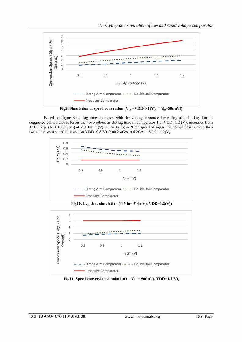
Fig9. Simulation of speed conversion (Vcm=VDD-0.1(V), ∆Vin=50(mV))
Based on figure 8 the lag time decreases with the voltage resource increasing also the lag time of
suggested comparator is lesser than two others as the lag time in comparator 1 at VDD=1.2 (V), increases from
161.037(ps) to 1.18659 (ns) at VDD=0.6 (V). Upon to figure 9 the speed of suggested comparator is more than
two others as it speed increases at VDD=0.8(V) from 2.8G/s to 6.2G/s at VDD=1.2(V).
Fig10. Lag time simulation (∆Vin= 50(mV), VDD=1.2(V))
Fig11. Speed conversion simulation (∆Vin= 50(mV), VDD=1.2(V))
0
1
2
3
4
5
6
7
0.8 0.9 1 1.1 1.2
Co
nve
rsio
n S
pee
d (
Gig
a /
Per
Se
con
d)
Supply Voltage (V)
Strong Arm Comparator Double-tail Comparator
Proposed Comparator
0
0.2
0.4
0.6
0.8
0.8 0.9 1 1.1
Del
ay (
ns)
Vcm (V)
Strong Arm Comparator Double-tail Comparator
Proposed Comparator
0
2
4
6
8
0.8 0.9 1 1.1
Co
nve
rsio
n S
pee
d (
Gig
a /
Per
Se
con
d)
Vcm (V)
Strong Arm Comparator Double-tail Comparator
Proposed Comparator

Designing and simulation of low and rapid voltage comparator
DOI: 10.9790/1676-11040198108 www.iosrjournals.org 106 | Page
Fig12. Suggested comparator lag time versus the voltage resource
Fig13.Suggested comparator lag time versus the input voltage resource domain
Table1. The suggested comparator properties
parameter
amount
technology
180-nm CMOS
Voltage resource
1.2 V
The amount of energy consumption in 100MHz frequency
(Vcm=1.1 V , ∆Vin= 25 mV)
15.194 (µW)
The worst state of lag time
( Vcm=0.6 V , ∆Vin= 1mV )
240.452 (ps)
The input voltage offset( os )σ,( 1-sigma)
3.658454 (mV)
energy efficiency
Vcm=1.1 V , ∆Vin= 25 mV) )
2.44 (fJ)
Energy in each cycle
Vcm=1.1 V , ∆Vin= 25 mV))
151.94 (fJ)
Speed ( Vcm=1.1 V , ∆Vin= 25 mV)
6.2 (Giga/per second)
Approximated chipset area
23.45 (um) * 14.505 (um)
0
0.2
0.4
0.6
0.8
0.8 0.9 1 1.1 1.2
Del
ay (
ns)
Supply Voltage (V)
∆Vin=5mV ∆Vin=10mV ∆Vin=50mV
∆Vin=100mV ∆Vin=200mV
0
0.05
0.1
0.15
0.2
0.25
Del
ay (
ns)
∆Vin (mV)
0.7 0.8 0.9 1

Designing and simulation of low and rapid voltage comparator
DOI: 10.9790/1676-11040198108 www.iosrjournals.org 107 | Page
Table2. Comparing the comparator properties
Comparator properties
Strong Arm
Double Tail
Suggested Comparator
Sampling maximum frequency
900MHz
1.8GHHz
900MHz
Kickback noise @(∆Vin=10mV)
55(mV)
6(mV)
44 (mV)
Each cycle energy
(Vcm=1.1 V)
∆Vin= 25 mV))
114.1 (fJ)
202.81 (fJ)
151.94 (fJ)
Energy efficiency
10.311 (fJ)
6.74 (fJ)
2.44 (fJ)
speed
(Giga/per second)
2
(Giga/per second )
2.94
(Giga/per second)
6.2
(Giga/per Second)
Input voltage offset
(os )σ,( 1-sigma()Vcm=1.1V)
4.02 (mV)
4.357 (mV)
3.658454 (mV)
Chipset approximated area
25.41 (um) * 14.77 (um)
31.295 (um) * 13.875 (um)
23.45 (um) * 14.505 (um)
Fig14. The suggested comparator layout
II. Conclusion
In this article, the complete analysis of dynamic comparators has been studied and their terms have
been extracted. Also two Strong Arm and Double Tail comparators have been analyzed, and based on analytical
analysis a fast and optimized low voltage comparator has been introduced. The simulation results and the
comparing performance table show the better performance of suggested comparators than the Strong Arm and
Double Tail comparators.
References: [1]. Tony Chan Carusone, David A. Johns, Kenneth W. Martin, ANALOG INTEGRATED CIRCUIT DESIGN, Second Edition
[2]. Yongfu Li, Wei Mao, Zhe Zhang, Yong Lian , 17-20 Nov. 2014 , An Ultra-Low Voltage Comparator with Improved Comparison
Time and Reduced Offset Voltage, Circuits and Systems (APCCAS), 2014 IEEE Asia Pacific Conference on ,pp 407 – 410. [3]. Halim, I.S.A. ; Fac. of Electr. Eng., Univ. Teknol. Mara, Shah Alam, Malaysia ; Abidin, N.A.N.B.Z. ; Rahim, A.A.A. , 28-30 Sept.
2011 , Low power CMOS charge sharing dynamic latch comparator using 0.18μm technology , Micro and Nanoelectronics (RSM),
2011 IEEE Regional Symposium on , pp156 – 160 [4]. Choi, R.Y.-K. ; Dept. of Electron. & Comput. Eng., Hong Kong Univ. of Sci. & Technol., Hong Kong, China ; Chi-ying Tsui , 5-8
Aug. 2012 , A novel offset cancellation technique for dynamic comparator latch , Circuits and Systems (MWSCAS), 2012 IEEE
55th International Midwest Symposium on , pp614 – 617. [5]. Wicht, B. ; Mixed-Signal Power & Control, Texas Instruments Deutschland GmbH, Freising, Germany ; Nirschl, T. ; Schmitt-
Landsiedel, D. , July 2004 , Yield and speed optimization of a latch-type voltage sense amplifier , Solid-State Circuits, IEEE Journal
of (Volume:39 , Issue: 7 ) , pp1148 – 1158 [6]. Babayan-Mashhadi, S. ; Electr. Eng. Group of Eng. Dept., Ferdowsi Univ. of Mashhad, Mashhad, Iran ; Lotfi, R. , 11 February
2013 , Analysis and Design of a Low-Voltage Low-Power Double-Tail Comparator , Very Large Scale Integration (VLSI) Systems,
IEEE Transactions on (Volume:22 , Issue: 2 ) , pp343 – 352 [7]. Figueiredo, P.M. ; Chipidea Microelectron. SA, Porto Salvo, Portugal ; Vital, J.C. , July 2006 , Kickback noise reduction techniques
for CMOS latched comparators , Circuits and Systems II: Express Briefs, IEEE Transactions on (Volume:53 , Issue: 7 ) , pp541 -
545
Designing and simulation of low and rapid voltage comparator
DOI: 10.9790/1676-11040198108 www.iosrjournals.org 108 | Page
[8]. Razavi, B. , Spring 2015 , The StrongARM Latch [A Circuit for All Seasons] , Solid-State Circuits Magazine,
IEEE (Volume:7, Issue: 2 ) , pp12 – 17
[9]. D. Shinkel, E. Mensink, E. Klumperink, E. van Tuijl, and B. Nauta, Feb. 2007 , “A double-tail latch-type voltage sense amplifier with 18ps Setup+Hold time,” in Proc. IEEE Int. Solid-State Circuits Conf.,Dig. Tech. Papers, pp. 314–315.


