
San Jose State University San Jose State University
SJSU ScholarWorks SJSU ScholarWorks
Master's Theses Master's Theses and Graduate Research
Fall 2016
Design and Analysis of a Low-Power 8-Bit 500 KS/S SAR ADC for Design and Analysis of a Low-Power 8-Bit 500 KS/S SAR ADC for
Bio-Medical Implant Devices Bio-Medical Implant Devices
Ehsan Mazidi San Jose State University
Follow this and additional works at: https://scholarworks.sjsu.edu/etd_theses
Recommended Citation Recommended Citation Mazidi, Ehsan, "Design and Analysis of a Low-Power 8-Bit 500 KS/S SAR ADC for Bio-Medical Implant Devices" (2016). Master's Theses. 4767. DOI: https://doi.org/10.31979/etd.tq8n-42kd https://scholarworks.sjsu.edu/etd_theses/4767
This Thesis is brought to you for free and open access by the Master's Theses and Graduate Research at SJSU ScholarWorks. It has been accepted for inclusion in Master's Theses by an authorized administrator of SJSU ScholarWorks. For more information, please contact [email protected].

DESIGN AND ANALYSIS OF A LOW-POWER 8-BIT 500 KS/S SAR ADC FOR
BIO-MEDICAL IMPLANT DEVICES
A Thesis
Presented to
The Faculty of the Department of Electrical Engineering
San José State University
In Partial Fulfillment
of the Requirements for the Degree
Master of Science
by
Ehsan Mazidi
December 2016

ii
© 2016
Ehsan Mazidi
ALL RIGHTS RESERVED

iii
The Designated Thesis Committee Approves the Thesis Titled
DESIGN AND ANALYSIS OF A LOW-POWER 8-BIT 500 KS/S SAR ADC FOR
BIO-MEDICAL IMPLANT DEVICES
by
Ehsan Mazidi
APPROVED FOR THE DEPARTMENT OF ELECTRICAL ENGINEERING
SAN JOSÉ STATE UNIVERSITY
December 2016
Dr. Shahab Ardalan Department of Electrical Engineering
Dr. Morris Jones Department of Electrical Engineering
Dr. Robert H. Morelos-Zaragoza Department of Electrical Engineering

iv
ABSTRACT
DESIGN AND ANALYSIS OF A LOW-POWER 8-BIT 500 KS/S SAR ADC FOR
BIO-MEDICAL IMPLANT DEVICES
by
Ehsan Mazidi
The presented thesis is the design and analysis of an 8-bit successive
approximation register (SAR) analog to digital convertor (ADC), designed for low-power
applications such as bio-medical implants. First we introduce the general concept of
analog to digital conversion, different methodologies, and architectures. Later, the SAR
architecture, used in this project, is explained in detail. The design and analysis of each
sub-system for the ADC system has been explained thoroughly. Novel comparator
architecture is proposed. This Bulk input comparator substantially reduces the overall
power consumption of the ADC system. All the circuits in this project were designed in
transistor level using 45 nm CMOS technology. The SAR logic was designed with
Verilog and then synthesized to be used in the ADC. The simulations were done in
analog mixed signal (AMS) mode. The sampling rate for the designed ADC is 500 KS/s
and the power consumption for the SAR ADC system was measured to be 2.1 µW. On
account of achieved performance and low power consumption of the designed SAR ADC
in this thesis; battery-less bio-implant devices are more feasible than ever.

v
DEDICATION
I would like to dedicate this work to my parents. Without their unconditional love and
support I would have never been able to reach this far and achieve this much. I owe them
all my success. I love you both.

vi
ACKNOWLEDGEMENTS
I would like to express my gratitude to my advisor, Dr. Shahab Ardalan, for
guiding me throughout this research with his invaluable knowledge. He has always
supported me, and my ideas in the course of my studies at San Jose State University. I
would also like to thank Dr. Ardalan for providing access to the Center for Analog and
Mixed Signal (AMS) lab. Without his guidance, this research would not have been
complete.
I would also like to thank thesis committee members, Dr. Morris Jones and Dr.
Robert Morelos-Zaragoza, for continuing to serve even in times of hardship. I am grateful
for their support and ideas throughout my education and research work at San Jose State
University.

vii
TABLE OF CONTENTS
LIST OF FIGURES ................................................................................................................................................... x
Introduction ................................................................................................................................................................. 1
Chapter 1. Analog to Digital Convertors ........................................................................................................... 2
The Need for ADC ............................................................................................................................................... 2
Block Diagram of ADC ...................................................................................................................................... 4
Sampling Rates ..................................................................................................................................................... 5
Anti-Aliasing Filter .............................................................................................................................................. 6
Comparator ............................................................................................................................................................. 8
Thermal to Digital Convertor ......................................................................................................................... 15
Chapter 2. Different Architectures in ADC ..................................................................................................... 18
Nyquist Rate ADC ............................................................................................................................................. 19
Flash ADC ....................................................................................................................................................... 20
Multistage ADC ............................................................................................................................................. 24
Pipeline ADC ................................................................................................................................................. 26
SAR ADC ........................................................................................................................................................ 40
Time-Interleaved (TI) Technique .................................................................................................................. 46
Hybrid Architectures ......................................................................................................................................... 48
Oversampling ADC ........................................................................................................................................... 50
Sigma-Delta ADC ......................................................................................................................................... 51
Chapter 3. SAR ADC ............................................................................................................................................. 55
SAR ADC Architecture .................................................................................................................................... 56

viii
SAR ADC Operation ......................................................................................................................................... 57
SAR Logic ............................................................................................................................................................ 59
SAR DAC ............................................................................................................................................................. 60
Chapter 4. Proposed SAR ADC Design ........................................................................................................... 62
State of the Art in Proposed Design ............................................................................................................. 63
Comparator Design ............................................................................................................................................ 64
Proposed DAC Design ...................................................................................................................................... 65
SAR Logic Design in Verilog ........................................................................................................................ 67
Sample and Hold Design.................................................................................................................................. 69
Chapter 5. AMS Test Simulation and Results ................................................................................................ 70
Setting AMS Configuration in Cadence ..................................................................................................... 70
connectLib Library ....................................................................................................................................... 70
Config view ..................................................................................................................................................... 71
Connect rules .................................................................................................................................................. 72
Sampler Test Results ......................................................................................................................................... 73
Ramp Input Test ............................................................................................................................................ 74
Sinusoidal Input Test ................................................................................................................................... 75
Comparator Test Result .................................................................................................................................... 76
Different Inputs .............................................................................................................................................. 76
Ramp Input Test ............................................................................................................................................ 80
Stress Test ........................................................................................................................................................ 81
DAC Test Result ................................................................................................................................................. 82
Different Binary Weighted Inputs to the DAC .................................................................................... 82

ix
DAC Stress Test ............................................................................................................................................ 88
SAR ADC Tests .................................................................................................................................................. 89
Test Result for DC Analog Input ................................................................................................................. 90
Conclusion ................................................................................................................................................................. 91
References .................................................................................................................................................................. 91

x
LIST OF FIGURES
Figure 1.1 Block diagram of analog to digital conversion system ....................................... 4
Figure 1.2 Noise and the concept of the anti-aliasing filter ........................................................ 7
Figure 1.3 Sampler configuration ....................................................................................................... 8
Figure 1.4 Quantization levels .......................................................................................................... 9
Figure 1.5 Ideal transfer function for comparator ................................................................. 11
Figure 1.6 Cascade of Open Loop Op-Amp ................................................................................ 13
Figure 1.7 Cross-coupled pair ........................................................................................................ 14
Figure 1.8 Thermal to binary circuit ........................................................................................... 16
Figure 1.9 Thermal to binary bubble correction circuit ...................................................... 17
Figure 2. 1 Flash ADC architecture .............................................................................................. 20
Figure 2. 2 Resistive ladder with 2-bit Flash ADC .................................................................. 22
Figure 2. 3 Pipeline ADC with four stages, each stage of 3-bit resolving 2 bits .......... 27
Figure 2. 4 General architecture of multistage ADC .............................................................. 28
Figure 2. 5 Gain architecture in multi-stage ADC ................................................................... 29
Figure 2. 6 Reducing the processing clock time ...................................................................... 29
Figure 2. 7 (a) Pipeline multistage architecture (b) Pipeline architecture ................... 30
Figure 2. 8 Digital correction logic ............................................................................................... 31
Figure 2. 9 Data latency concept ................................................................................................... 32
Figure 2. 10 Single-Stage Pipeline model .................................................................................. 33
Figure 2. 11 Pipeline Structure model ........................................................................................ 34
Figure 2. 12 Overall architecture of ADC ................................................................................... 35

xi
Figure 2. 13 Improved T/H in Pipeline ADC ............................................................................ 35
Figure 2. 14 Alternative to gain and DAC stage in Pipeline ................................................ 36
Figure 2. 15 Pipeline architecture at 1.5 bit stage ................................................................. 37
Figure 2. 16 (a) ADC architecture with SHA (b) ADC architecture without SHA ........ 39
Figure 2. 17 Suggestion for cascading additional stages ..................................................... 40
Figure 2. 18 SAR architecture .......................................................................................................... 41
Figure 2. 19 DAC output waveform ............................................................................................... 42
Figure 2. 20 Charge redistribution architecture ........................................................................... 44
Figure 2. 21 Example of DAC architecture ................................................................................. 46
Figure 2. 22 (a) Interleaved architecture (b) Clocking sequence ............................................ 47
Figure 2. 23 A cascaded hybrid ∑∆ ADC architecture ............................................................. 49
Figure 2. 24 A second-order sigma-delta modulator.................................................................. 50
Figure 2. 25 Derivation of Sigma-Delta modulation from delta modulation
(modified from [19]) .................................................................................................... 52 Figure 2. 26 Block Diagram of Sigma-Delta Modulation (modified from [19]) ............... 53
Figure 2. 27 S-Domain Analysis of Sigma-Delta Modulator (modified from [19]) ......... 54
Figure 2. 28 Block Diagram of First-Order Σ∆ ADC converter (modified from [19]) .... 55 Figure 3.1 SAR architecture ............................................................................................................ 57
Figure 3.2 SAR decision-making process ................................................................................. 59
Figure 3. 3 Resistive DAC architecture ....................................................................................... 61
Figure 3.4 Switched capacitor DAC architecture .................................................................... 61
Figure 4. 1 Designed SAR ADC architecture ............................................................................. 62
xii
Figure 4. 2 Proposed comparator architecture ....................................................................... 64
Figure 4. 3 Designed DAC architecture ...................................................................................... 65
Figure 4. 4 Architecture for the internal switch used in DAC ............................................ 66
Figure 4. 5 Sampler architecture .................................................................................................. 69 Figure 5. 1 Library path for connectLib ..................................................................................... 71
Figure 5. 2 Connect rule selection ................................................................................................. 72
Figure 5. 3 Setting the values for connect rules ...................................................................... 73
Figure 5. 4 Sampler test bench ...................................................................................................... 74
Figure 5. 5 Sampler ramp test ........................................................................................................ 74
Figure 5. 6 Sampler ramp test (zoomed) ................................................................................... 75
Figure 5. 7 Sampler sinusoidal input test .................................................................................. 75
Figure 5. 8 Sinusoidal input (zoomed) ....................................................................................... 76
Figure 5. 9 Comparator test bench............................................................................................... 76
Figure 5. 10 Comparator test result ............................................................................................ 77
Figure 5. 11 Comparator test result ............................................................................................ 77
Figure 5. 12 Comparator test result ............................................................................................ 78
Figure 5. 13 Comparator test result ............................................................................................ 78
Figure 5. 14 Comparator test result ............................................................................................ 79
Figure 5. 15 Comparator test result ............................................................................................ 80
Figure 5.16 Comparator ramp test result ................................................................................. 81
Figure 5. 17 Comparator stress test result ............................................................................... 81
Figure 5.18 DAC test bench ............................................................................................................. 82

xiii
Figure 5. 19 DAC test result ............................................................................................................ 83
Figure 5. 20 DAC test result ............................................................................................................ 83
Figure 5. 21 DAC test result ............................................................................................................ 84
Figure 5. 22 DAC test result ............................................................................................................ 85
Figure 5. 23 DAC test result ............................................................................................................ 85
Figure 5. 24 DAC test result ............................................................................................................ 86
Figure 5. 25 DAC test result ............................................................................................................ 86
Figure 5. 26 DAC test result ............................................................................................................ 87
Figure 5. 27 DAC test result ............................................................................................................ 87
Figure 5. 28 DAC test result ............................................................................................................ 88
Figure 5. 29 DAC stress test result ............................................................................................... 89
Figure 5.30 Proposed SAR test bench ......................................................................................... 90
Figure 5. 31 Test result for proposed SAR ................................................................................ 90

1
Introduction
In the ever-growing semiconductor industry, many applications require specific
solutions and therefore unique circuitry in order to complete the desired task. For
example, in medical applications involving human well-being, one cannot just pick a
random design from the shelf and expect that to fulfill the needs and requirements for that
specific task. Every application in bio-implant devices requires a costume design.
The analog to digital converter (ADC) is one of the most important building
blocks in any electronic device. The successive approximation register (SAR) ADC is
one of the most common architectures in medical applications due to its low power
consumption and simplicity of architecture. However, this does not mean that a
ubiquitous SAR ADC architecture and design can be used in all medical chips and
devices.
Based on the application and designed task for implant of sensors or chips,
integrated circuit (IC) designers tend to propose a unique SAR design both in architecture
and circuitry. This is exactly what has been done in this thesis. This work is based on the
requirements of a deep-brain stimulator device.
New advances in electrical engineering have created novel opportunities in almost
every field of science and one of the most important of these is medical engineering. The
motivation behind this work is to apply these new advances in semiconductor industry in
solving real life problems.
One of the major challenges facing medical science is the inability to monitor and
respond to the human body instantaneously. However, new advances in sensor
technology and the downscaling of transistor size provide the ability to implant those
2
sensors in order to monitor critical human vitals and give a real-time response. However,
when a monitoring device is implanted in the human body, one expects the device's
battery to have the same lifetime as long as the patient. This means the electronic device
needs to be extremely low power consuming.
The main sources of power consumption in most electronic devices are the analog
parts, and the main consumer of power in the analog circuitry is the ADC. Therefore,
ADC power consumption reduction for bio-implants devices has been the main focus in
this work.
Chapter 1. Analog to Digital Convertors
The Need for ADC
Natural phenomena in nature, such as sound or light, are purely analog
(continuous signal). Different types of sensors translate temperature, pressure and other
natural parameters to analog format, such as voltage or current.
Data conversion is when a signal is converted from one state to another. There are
various types of data conversions, for example time to digital conversion (TDC).
However, the main conversion is analog to digital conversion or ADC. In ADC, an
analog input signal is quantized and converted to a digital representation of that signal.
One might wonder why there is a need for data conversion. Why can’t all
processing and computing be performed on the input signal in the analog domain? The
answer is the rising need for higher and more complex processing of data. Processing a
signal requires mathematical or calculations that can sometimes be very complex. This
complexity in computation means that the electrical signal should be presented in a

3
quantized manner in order to be operable in mathematical calculations, hence the need for
a digital domain.
On the other hand, a natural phenomenon is analog, or continuous, meaning that
any reading from natural phenomena such as light or sound would translate into analog
signals. Therefore, in order to conduct analysis of those signals, the analog domain must
be converted to digital, and vice versa. This requires data convertors such as an ADC or
a digital to analog convertor (DAC) that converts digital values to their analog
representation. The need for a DAC is obvious, as humans cannot understand machine
language. Computed signals must be converted back into their original analog format,
such as sound or light, in order to be understood by people.
In order for digital devices to operate, sensors must translate physical phenomena
to electrical representations that are analog, or continuous. Through data conversions,
analog signals are quantized for digital signal processing and other computations. In
order to digitize an analog signal, not only does one have to quantize the continuous
signal in time domain, but also the value of the signal needs to be quantized so that the
machine can understand it. Machine language is a binary system, meaning that it
generates values of 0s and 1s with respect to a reference at a certain point of time, with a
certain set of values of that signal. The system that quantizes the analog signal in time
and generates specific sets of values in time is called a sampler, and the system, which
generates 1 or 0 with respect to a certain reference, is called a comparator. More on these
topics is presented below.

4
Block Diagram of ADC
To better understand a system, engineers divide that system into different
subsystems, which are in turn divided into multiple sections called blocks. A block
diagram is a top-level design which shows the main components of a system, whether
that system be electrical, mechanical, biological or even chemical. In the field of
electronics, every subsystem in every device has its own block diagram. The block
diagram in analog to digital data conversion consists of four blocks; see Figure 1.1:
Anti-Aliasing Filter
Time Quantization
Level Quantization
Thermal to Binary Convertor
Figure 1.1 Block diagram of analog to digital conversion system
As mentioned earlier, in order to digitize an analog signal, the data signal should
be quantized both in time and voltage levels. However, the input data link usually carries
unwanted signals referred to as noise. In order to only sample the desired signal and
reduce noise, the input signal is first fed to a filtering block called anti-aliasing. After
extracting the desired signal, the signal would then be quantized with respect to time
using a sampler. The sampled signal is only digitized in time and cannot be processed

5
since the value of each quantized point of the signal is unclear. Quantizing the level of
the signal is done through the next block that is the comparator.
After quantizing the signal time and level, those values are still ambiguous to
processing units as they are still not yet in a mathematical binary system. The last block
in ADC converts the digitized values into binary equivalents for digital processors to
compute. Based on the application of the electronic device, a different level of conversion
is required. For sensitive applications such as aviation, a very fast and accurate level of
data conversion is required. That is why for each application a different sampling rate and
bit number are applied, which translates to a different level of speed and accuracy for the
data conversion.
Sampling Rates
A time quantization block works at a certain frequency, which is referred to as the
sampling frequency. Sampling theorem is based on the fact that, in order for other
processing units to be able to reconstruct the original continuous signal from its discrete
format, time quantization should occur at a certain frequency, called the Nyquist
frequency. The Nyquist frequency dictates that the sampling frequency of the time
quantization block should be at least twice that of the input frequency. This requirement
puts a certain constraint on the ADC system. In order to convert high frequency signals, a
much higher sampling frequency is required.
Another constraint on the Nyquist frequency is that the time quantization block
samples any signal that is lower than the sampling frequency, meaning that an entire band
of undesired signals may be sampled. In order to prevent the conversion of incorrect data,
ADC designers must filter the input signal using an anti-aliasing filter, so that only the

6
band of interest passes through the sampling block. The anti-aliasing filter is placed
before any other block of the ADC in order to filter out undesired signals, so that the time
quantization block is able to sample signals in the desired band of interest.
Anti-Aliasing Filter
The input signal to the data conversion is analog and continuous in all
frequencies; however, only a small bandwidth in a given signal targeted for data
conversion. If one converts the entire input signal, this may also convert unwanted noise
signals in other frequencies, which would corrupt the desired signal. Moreover, the
thermal noise presents in electronic elements poses a potential risk of degrading or even
corrupting the value of the signal. For this reason, all unwanted frequencies must first be
filtered out in order to reduce the overall noise and prevent incorrect data conversion.
Furthermore, thermal noise is a major component of noise in wideband signals. If the
designer were to take the entire input frequency and convert it into digital, thermal noise
would affect the original signal and corrupt the digital value of the conversion. Figure 1.2
illustrates this concept.
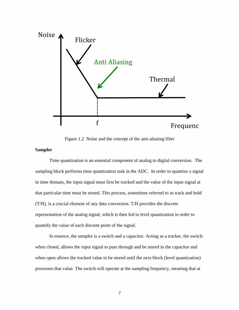
7
Figure 1.2 Noise and the concept of the anti-aliasing filter
Sampler
Time quantization is an essential component of analog to digital conversion. The
sampling block performs time quantization task in the ADC. In order to quantize a signal
in time domain, the input signal must first be tracked and the value of the input signal at
that particular time must be stored. This process, sometimes referred to as track and hold
(T/H), is a crucial element of any data conversion. T/H provides the discrete
representation of the analog signal, which is then fed to level quantization in order to
quantify the value of each discrete point of the signal.
In essence, the sampler is a switch and a capacitor. Acting as a tracker, the switch
when closed, allows the input signal to pass through and be stored in the capacitor and
when open allows the tracked value to be stored until the next block (level quantization)
processes that value. The switch will operate at the sampling frequency, meaning that at
Flicker noise
Thermal noise
Anti Aliasing Filter
Frequency
Noise
f

8
the sampling clock edge the switch will be open and thus the sampler will be in hold
mode. Figure 1.3 illustrates s the basic concept of the sampler.
Figure 1.3 Sampler configuration
Comparator
As mentioned above, the comparator is the level quantization block in the ADC
architecture. This block is responsible for reporting the relative value of the input signal,
which is then compared to a predetermined reference value. The comparator contrasts the
input signal with different reference values in order to determine the digital
representation of the input signal. By combining the information from time quantization
and the respective analog values of that signal at the time of sampling, one can represent
an analog signal with its digital equivalent.
Therefore, a comparator is the basis for level quantization. It is where the actual
digitization takes places, as the inputted analog values will now be represented by digital
equivalents. However, to represent an analog signal accurately one must digitize the input
signal value based on different incremental levels.

9
The accuracy level of digital representation of an analog signal depends mainly on
the number of digital bits in the representation. This means that, the higher the number of
digital bits, the more accurate the digital signal is when compared to its original analog
signal. The quantization block must somehow generate different reference values with
respect to the input signal’s full range swing.
As it can be seen in Figure 1.4, in order to represent an analog input signal with
three bits of its digital equivalent, the system requires 8 levels of quantization to cover the
full range of swing for the input signal in this case, 23-1 reference levels. This trend
holds for any number of bits, meaning that for an N-bit digital representation nN-1
reference levels are needed. The higher the number of bits, the higher the resolution or
the accuracy of the digital representation is.
Figure 1.4 Quantization levels
10
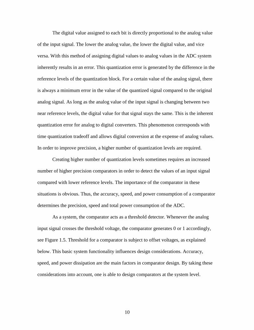
The digital value assigned to each bit is directly proportional to the analog value
of the input signal. The lower the analog value, the lower the digital value, and vice
versa. With this method of assigning digital values to analog values in the ADC system
inherently results in an error. This quantization error is generated by the difference in the
reference levels of the quantization block. For a certain value of the analog signal, there
is always a minimum error in the value of the quantized signal compared to the original
analog signal. As long as the analog value of the input signal is changing between two
near reference levels, the digital value for that signal stays the same. This is the inherent
quantization error for analog to digital converters. This phenomenon corresponds with
time quantization tradeoff and allows digital conversion at the expense of analog values.
In order to improve precision, a higher number of quantization levels are required.
Creating higher number of quantization levels sometimes requires an increased
number of higher precision comparators in order to detect the values of an input signal
compared with lower reference levels. The importance of the comparator in these
situations is obvious. Thus, the accuracy, speed, and power consumption of a comparator
determines the precision, speed and total power consumption of the ADC.
As a system, the comparator acts as a threshold detector. Whenever the analog
input signal crosses the threshold voltage, the comparator generates 0 or 1 accordingly,
see Figure 1.5. Threshold for a comparator is subject to offset voltages, as explained
below. This basic system functionality influences design considerations. Accuracy,
speed, and power dissipation are the main factors in comparator design. By taking these
considerations into account, one is able to design comparators at the system level.

11
Figure 1.5 Ideal transfer function for comparator
To meet the requirements for accuracy, gain resolution and offset should be taken
into account. Gain resolution is the required gain for the comparator as a system to
amplify the minimum differential input voltage to the maximum allowed voltage, Vdd.
The goal is to detect the smallest allowable differential input voltage and amplify that to
Vdd. By introducing the concept of least significant bit (LSB), one is able to measure the
required gain mathematically. The mathematical expression for LSB or is as follows,
where FSR is the full swing range of the input signal and N is the number of bits of the
ADC:
(1.1)
The higher the number of ADC bits, the lower the value of delta, . The required
gain resolution is defined based on LSB. For a resolution of /n of differential input, the
required gain can be calculated as:
12
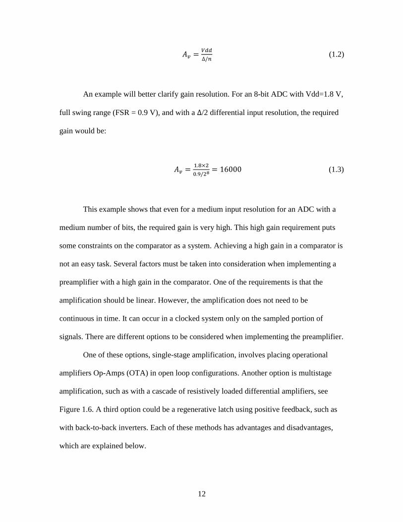
(1.2)
An example will better clarify gain resolution. For an 8-bit ADC with Vdd=1.8 V,
full swing range (FSR = 0.9 V), and with a /2 differential input resolution, the required
gain would be:
(1.3)
This example shows that even for a medium input resolution for an ADC with a
medium number of bits, the required gain is very high. This high gain requirement puts
some constraints on the comparator as a system. Achieving a high gain in a comparator is
not an easy task. Several factors must be taken into consideration when implementing a
preamplifier with a high gain in the comparator. One of the requirements is that the
amplification should be linear. However, the amplification does not need to be
continuous in time. It can occur in a clocked system only on the sampled portion of
signals. There are different options to be considered when implementing the preamplifier.
One of these options, single-stage amplification, involves placing operational
amplifiers Op-Amps (OTA) in open loop configurations. Another option is multistage
amplification, such as with a cascade of resistively loaded differential amplifiers, see
Figure 1.6. A third option could be a regenerative latch using positive feedback, such as
with back-to-back inverters. Each of these methods has advantages and disadvantages,
which are explained below.

13
Figure 1.6 Cascade of Open Loop Op-Amp
Using an Op-Amp as a preamplifier would produce a certain amount of gain.
However, the time it would take for a single stage Op-Amp to amplify the input signal
and achieve the required gain for the system is too long for the ADC to handle.
Therefore, a single-stage amplifier is not the best option. Another problem with the Op-
Amp as a comparator is that mismatches can cause offset and gain errors.
Multistage amplification, such as cascade of resistively loaded differential
amplifiers, enables the comparator to generate the required gain much more quickly.
Despite the gain, there are some drawbacks to this architecture. One major disadvantage
is that the resistive load is subject to huge process variation (PVT) in which the desired
gain might not be achieved due to mismatches between the design factors and the actual
values of the resistive loads. Another option would be to use a cascade of integrators as
amplifiers, thus eliminating the resistive load and increasing the gain at each stage. This
increased gain would reduce the required time for achieving the desired gain resolution.
Employing a cross-coupled regenerative sense amplifier or latch is one of the
preferred options for the pre-amplified stage. The cross-coupled pair is one of the most

14
commonly used preamplifier stages in today’s state-of-the-art comparator design. Figure
1.7 illustrates the concept of the cross-coupled pair.
Figure 1.7 Cross-coupled pair
Another option for achieving high gain would be to use a regenerative latch, in
the form of a back-to-back inverter. This topology is widely implemented in comparator
design due to its high amplification speed and gain. With this topology digitization of the
input signal can be quickly achieved, since an inverter can be used to generate only two
logical voltages, Vdd or logical 1 and ground (GND) or logical 0. The latch in a back-to-
back inverter also helps in keeping the generated digit at the output node. However,
while a back-to-back inverter offers a high linear gain and fast response time to input
signals, the drawback with back-to-back inverter topology is the offset.
As mentioned earlier, offset is an undesired phenomenon in a comparator for
several factors, including device mismatch in cross-coupled pairs and, most importantly,
metastability in back-to-back inverters. Offset is the mismatch between the designed
threshold voltage of the comparator and the actual threshold voltage. This mismatch in
threshold voltage causes the comparator to report incorrect outputs due to the fact that

15
while the input voltage has crossed the designed value of threshold voltage, the output
voltage remains at zero.
Offset is an inherent, unavoidable characteristic of comparators. One of the
principal causes of offset is metastability in back-to-back inverters. Metastability occurs
when the input signal is stuck in a region where both the PMOS and NMOS are switching
from saturation to the cutoff region. The voltage value for this region is usually Vdd/2.
At this point, with both transistors working against each other, the PMOS attempts to
switch the output to high voltage while the NMOS is tries to take the output to ground.
At this point the output voltage becomes stuck between Vdd and ground (Vdd/2), and no
logical output is generated. Depending on the CMOS technology, the metastability region
varies from tens of millivolts to hundreds of millivolts. Nonetheless, there are methods
for reducing comparator offset that will be discussed later on.
The fact remains that latches, such as back-to-back inverters, which offer high
linear gain and fast digitization, inherently produce offsets. Whether this involves cross-
coupled pair offset due to device mismatch or back-to-back metastability, latch offset
dictates a certain methodology in comparator design. A preamplifier is needed to amplify
the input differential voltage to such a level that it would not be affected by latch offset or
get stuck in the metastability region. Therefore, from the system point of view, a
comparator consists of two blocks, preamplifier and latch.
Thermal to Digital Convertor
The last step in the analog to digital conversion is generating the binary values for
the analog signal. At this point the analog signal has passed through the sampler and the
comparator and has been quantified in time and level. However, the discrete quantified

16
signal is not in binary form. To convert to a binary system, another circuit is needed,
which is referred to as thermal to binary. The idea is to treat a certain value of the signal
at a certain point in time as if it were a thermal reading on a thermometer. Each level
represents a value and is assigned to a binary code. The circuit for this conversion is
fairly simple. Figure 1.8 illustrates the concept of thermal to binary conversion for a
simple 4-bit binary code circuit schematic.
Figure 1.8 Thermal to binary circuit
As in any other system, glitches occur in thermal to binary conversion. For
example, if one of the thermal codes in the ADC is wrong, this may result in an incorrect
conversion. An inaccurate thermal code can result from several different causes; two of
the most common being inherent offset in the comparator and a faulty an input signal that
is very close to the reference point.

17
An inaccurate code may also be the result of a lack of speed in the comparator.
When the comparator is slow, a 0 may be generated instead of the correct code of 1.
When a0 code appears between 1's, we refer to it as a bubble. A bubble can cause a faulty
binary conversion in the final thermal to binary conversion. One of the simplest ways to
correct this error is to use three inputs AND gates in order to double check the integrity
of the thermal code. Figure 1.9 shows this architecture for a bubble correction circuit.
Figure 1.9 Thermal to binary bubble correction circuit

18
Chapter 2. Different Architectures in ADC
Just as there are different possible methods of finding the solution to a
mathematical problem, there are various ways in which an analog signal can be converted
into a digital signal. However, several architectures exist for data conversion based on
standard methodologies in ADC architecture. Most electrical engineers divide ADC
architecture into two major types:
Nyquist Sampling Rate
Oversampling
These categorizations are based on the sampling rate at which the ADC operates.
As already mentioned, in order to digitize an analog signal, one should first quantize that
signal in time. The rate at which time quantization takes place is called the sampling
frequency. The Nyquist theorem explains the minimum requirements for sampling an
analog signal in order to digitize it and be able to reconstruct it later on. Based on this
theorem, the minimum sampling frequency for analog to digital conversion is twice the
frequency of the input analog signal. This rate is referred to as the Nyquist rate ADC.
The ADC sampling frequencies sometimes go as high as 10 times the input frequency.
The ADC architectures that work with these rates are considered Nyquist ADC.
The other type of ADC based on the sampling rate is the oversampling ADC. In
the oversampling ADC, the sampler operates frequencies higher than 10 times the analog
input frequency. Oversampling ADCs usually operate at sampling rates of 100 times the
frequency of the input signal. There is only one major architecture that uses oversampling
technique, and that is the sigma-delta modulator ADC.

19
Nyquist Rate ADC
For the analog to digital conversion process to be beneficial, there must be a clear
structure on which the ADC system operates. One of those structures is sampling or time
quantization. Time quantization is essential to data conversion; however, the rate at
which the analog signal is being quantized is not completely set in the ADC structure. As
explained earlier, the Nyquist theorem tries to explain and construct a set of rules and
formulas according to which ADC sampling is to be operated.
Based on the Nyquist theorem, the sampling frequency should be at least twice
the analog frequency, allowing the DAC to be able to reconstruct the analog signal based
on the digital representation of that signal. However, because of other constrains and
limitations, the pragmatic sampling rate is often more than twice as high as the analog
signal frequency. Conversely, the sampling rate almost never exceeds 10 times that of the
analog frequency that is being sampled.
Based on aforementioned definition and the structure for time quantization and
sampling; any ADC architecture that uses the Nyquist theorem and has a sampling
frequency twice that of the analog input frequency will be referred to as the Nyquist rate
ADC. Most of the ADC architectures operate with the Nyquist sampling rate.
There are different reasons as to why Nyquist rate ADCs are preferred by IC
designers. The two main reasons for this preference are simplicity and speed. Although
Nyquist rate ADCs are not always power efficient, nor do they have the highest
resolution. The simplicity of their structure and the speed they offer in data conversion,
make them the preferred structure for most analog mixed signal (AMS) IC designers.
20
In the next sections we will explain these different Nyquist rate ADC
architectures. We will explain the differences in each architecture, advantages and
disadvantages of each, and also limitations in terms of speed, power and accuracy.
Flash ADC
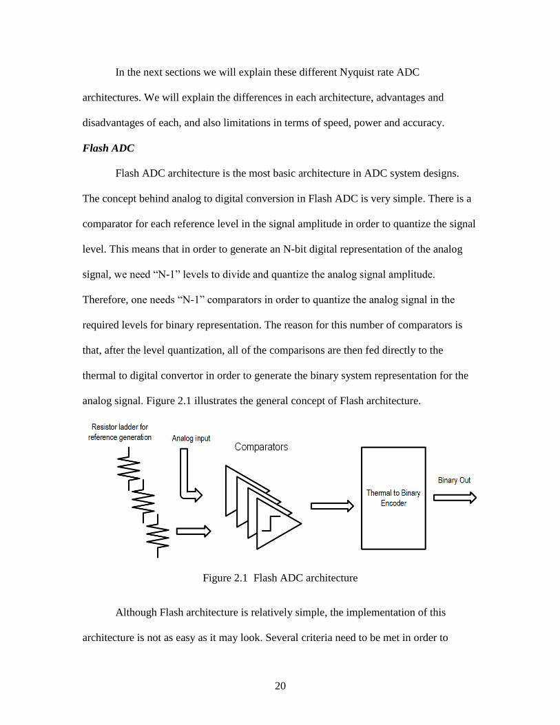
Flash ADC architecture is the most basic architecture in ADC system designs.
The concept behind analog to digital conversion in Flash ADC is very simple. There is a
comparator for each reference level in the signal amplitude in order to quantize the signal
level. This means that in order to generate an N-bit digital representation of the analog
signal, we need “N-1” levels to divide and quantize the analog signal amplitude.
Therefore, one needs “N-1” comparators in order to quantize the analog signal in the
required levels for binary representation. The reason for this number of comparators is
that, after the level quantization, all of the comparisons are then fed directly to the
thermal to digital convertor in order to generate the binary system representation for the
analog signal. Figure 2.1 illustrates the general concept of Flash architecture.
Figure 2.1 Flash ADC architecture
Although Flash architecture is relatively simple, the implementation of this
architecture is not as easy as it may look. Several criteria need to be met in order to

21
perform reliable and accurate data conversion. Due to the high number of comparators in
Flash architecture, comparator design is of the highest importance. The values of the
offset and the comparator speed are two crucial factors in the accuracy and reliability of
Flash architecture.
As explained previously, a comparator requires two inputs, one of which acts as
the reference voltage or level for the other input, which acts as the analog input.
Therefore, in the case of Flash ADC, the IC designer has to generate certain voltage
reference levels, most commonly through resistive ladders.
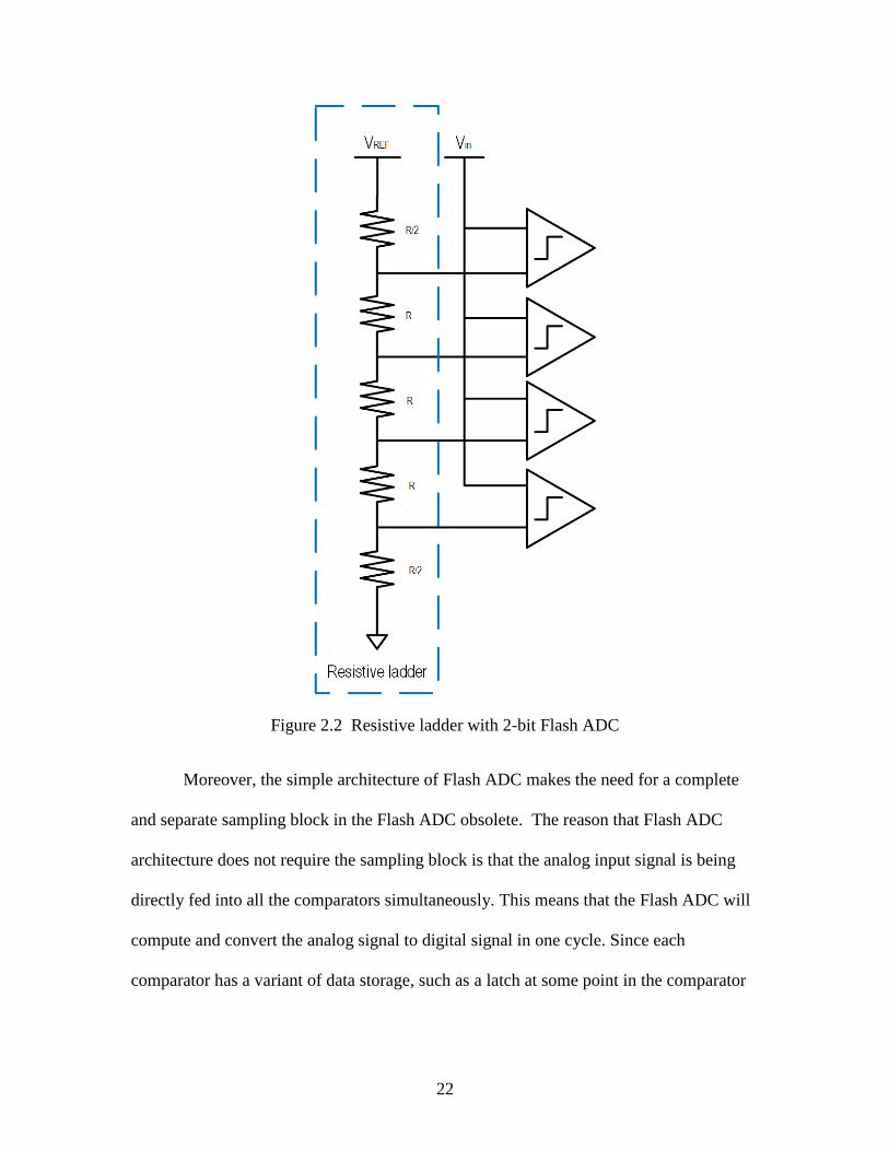
A resistive ladder is composed of resistors in series consisting of the same value.
However, after each resistance there is an output signal going to the reference node of the
comparator. The idea is very simple: through voltage division over the resistive ladder
one can generate the required voltage levels. This also means that designers need the
same number of resistances, as there are levels in the Flash ADC. Figure 2.2 shows the
resistive ladder concept along with a full 2-bit Flash ADC.
22
Figure 2.2 Resistive ladder with 2-bit Flash ADC
Moreover, the simple architecture of Flash ADC makes the need for a complete
and separate sampling block in the Flash ADC obsolete. The reason that Flash ADC
architecture does not require the sampling block is that the analog input signal is being
directly fed into all the comparators simultaneously. This means that the Flash ADC will
compute and convert the analog signal to digital signal in one cycle. Since each
comparator has a variant of data storage, such as a latch at some point in the comparator
23
architecture that latch can act as the sampler and therefore there is no need for a separate
sampling block.
The main advantage of Flash ADC architecture is speed. This speed derives from
the fact that the analog input signal in ADC architecture is fed into all the comparators
simultaneously. The other main attraction of Flash ADC is the simplicity in architecture.
With Flash ADC architecture, there is no digital decision-making involved in data
conversion.
On the other hand, there are many disadvantages to Flash ADC architecture. The
main disadvantage is the limited accuracy of Flash ADC. This shortcoming is due to the
inherent design architecture. Flash ADC architecture requires one comparator for each
decision level, which means that the AMS IC designer must use 2N-1 comparators for an
N-bit data conversion with Flash ADC architecture. Highly accurate data conversion
requires more than 10 bits. This amounts to1023 comparators for a single Flash ADC,
which is simply not feasible. Evidence of this is that there are no 10-bit Flash ADC's
either in academia or industry. There are various complications that would prevent such
high-bit Flash ADC architecture from being possible from process variations in resistance
manufacturing that would prevent an even distribution of reference voltages over the
comparators to the inherent offset in comparators due to metastability that would prevent
the comparator from being able to detect small incremental differences in input voltages
and voltage references. All these constraints prevent an IC designer from designing a
Flash ADC with a high number of bits.
There is another downside to Flash ADC architecture, and that is the high power
consumption. Comparators are the main power consumers in ADC systems, and because

24
there are many comparators in ADC architecture the power consumption in Flash ADC
would soar so high that it would make it unviable to design a Flash ADC with a high
number of bits. For this reason, there are very few Flash ADC devices with more than 6
bits. And to the best of the author’s knowledge, there is no Flash ADC with more than 8
bits.
Flash ADC architecture is very simple and fast, making it IC designers’ choice for
ADC architecture in high-speed applications where speed is top priority. Also, in
applications where a low number of bits are enough to handle the task, Flash ADC
architecture is the first choice because of its simplicity.
Multistage ADC
The idea behind multi-stage ADC is to design an ADC system with the simplicity
of the Flash ADC architecture but with fewer comparators. Reducing the number of
comparators has many advantages in ADC design. By reducing the total number of
comparators used in ADC, designers can substantially reduce area and power
consumption. Also, because of the architecture of multi-stage ADC, AMS designers can
increase the number of bits in their ADC design, thereby increasing the analog to digital
conversion accuracy.
The architecture of multi-stage ADC is similar to Flash ADC, except that the
signal is digitized in multiple stages, where each stage is a Flash ADC designed to
quantize the amplitude level of a specific portion of the analog signal. Each stage will
generate a few of the total number of bits. The first stage will generate the most
significant bit (MSB) and the second stage will generate the LSB. This trend continues

25
from the highest value bits to the lowest value bits. The operating procedure of multi-
stage ADC is as follows.
The analog input signal is fed into the first stage (an N-bit Flash ADC) after the
previous stage has level quantized the analog signal. The decision at the first stage will be
sent to the second stage through subtraction. This means that the part of the analog signal
that is in the level quantization portion will be passed on to the next stage. In the second
stage, an M-bit Flash ADC will quantize the remaining portion of analog signal.
Theoretically, this process can continue forever; however, there are physical limitations
to this architecture that would make it impossible to continue beyond more than a few
stages. The total number of bits in this architecture is equal to the sum of the number of
bits in all stages. For example, in a three-stage ADC where the first stage has “G” number
of bits, the second stage “M” bits, and the third stage “K” bits. The total number of bits
for that Multi-stage ADC is expressed as N = G+M+K.
A simple comparison between this architecture and Flash ADC architecture
reveals that the total number of comparators in a multi-stage ADC is substantially lower
when compared to the Flash ADC architecture. For example, in a two-stage ADC where
each stage has a 3-bit Flash ADC, the total number of bits for this multi-stage ADC is
3+3=6; however, the total number of comparators is 2×(2^3)-1=14, where a 6-bit Flash
ADC has (2^6)-1 = 63 comparators. Therefore, in terms of area and power consumption,
there is no real competition between these two architectures. With a higher number of
bits, the Flash ADC has a very large number of comparators that require a large area and
consume huge amounts of power.
26
However, there is a downside to this architecture and that is the range of
amplitude levels that are fed into the comparators. The same values apply to reference
voltages in a multi-stage ADC as do to N-bits the same N-bit Flash ADC. Because of the
inherent offset and errors from the comparator, when the references stay the same at
some point the comparator will not be able to detect the difference between the analog
input value and the reference value.
The main advantage of multi-stage ADC is power conservation. The relatively
small number of comparators translates to lower area and lower power consumption.
However, this architecture offers high speed in terms of analog to digital conversion, with
only a few stages that operate in consequence. The final conversion will be delivered
with a delay.
Pipeline ADC
Pipeline ADC is one of the most popular ADC architectures because of its size,
resolution, high speed, and low power dissipation. It can sample data from a few mega-
samples per second to 100 mega-samples per second. Resolution ranges from 8 bits to
16 bits. Due to all these characteristics, pipeline ADCs have a wide variety of
applications, including CCD imaging, ultrasonic medical imaging, digital receivers,
HDTV, DSL cable and fast Ethernets.
Pipeline ADC Architecture:
As one can see from Figure 2.3, every stage is comprised of three key elements to
create a 12-bit pipelined ADC: a 3-bit Flash ADC, a 3-bit DAC, and a sample and hold
(S/H) circuit. The input voltage (Vin) is applied to both the S/H circuit and to the 3-bit
Flash ADC. Sample and hold will sample the data and feed it to the summation element.

27
On the other hand, Flash ADC quantizes the input voltage Vin into 3 bits. The digital
output of the Flash ADC is applied to two elements, one being the 3-bit DAC which
gives us the analog output and the other being time alignment and digital error correction.
This analog output is subtracted from the original input Vin in an adder element. The
"residue" output of the adder element experiences an increase in gain of a factor of four.
This output is then fed to Stage 2, where the same procedure will go on until the input
reaches the last stage. This residue gain from Stage 1 continues through the pipeline with
each stage providing 3 bits. Since we get 3 bits from each stage at different points of
time, we must perform time alignment with shift registers.
Figure 2.3 Pipeline ADC with four stages, each stage of 3-bit resolving 2 bits
Following the time alignment, we can feed this data to the data error correction
logic. After each stage finishes the process of sampling the data, observing the bits, and
finding the residue for the next stage, it will start processing the next sample received
from the sample & hold circuit within each stage. For this reason, pipeline ADCs have
high throughput.

28
Multi-Step ADC Issues:
As can be seen in Figure 2.4, this architecture contains a coarse ADC, a DAC, and
a B2-bit Fine ADC. The output of the coarse ADC will provide the MSB's and will also
be fed to the DAC. From here, the output of the DAC will be fed into the subtraction in
order to achieve a residue equivalent to Vin -VDAC. The fine ADC will use this residue as
its input and give the LSB as an output.
Figure 2.4 General architecture of multistage ADC
This architecture does create some issues:
1) The precision of fine ADC must be in the order of the overall ADC’s half LSB.
This problem can be solved by using the following architecture (Figure 2.5), in which a
gain stage was added with a gain of G = 2B1
= 4 prior to the fine ADC. The precision
required for fine ADC is only reduced by 2 bits in this case.
29
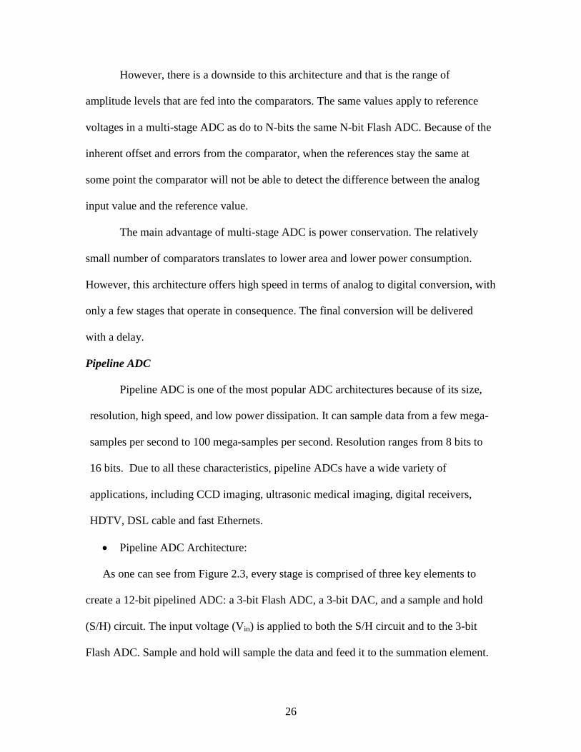
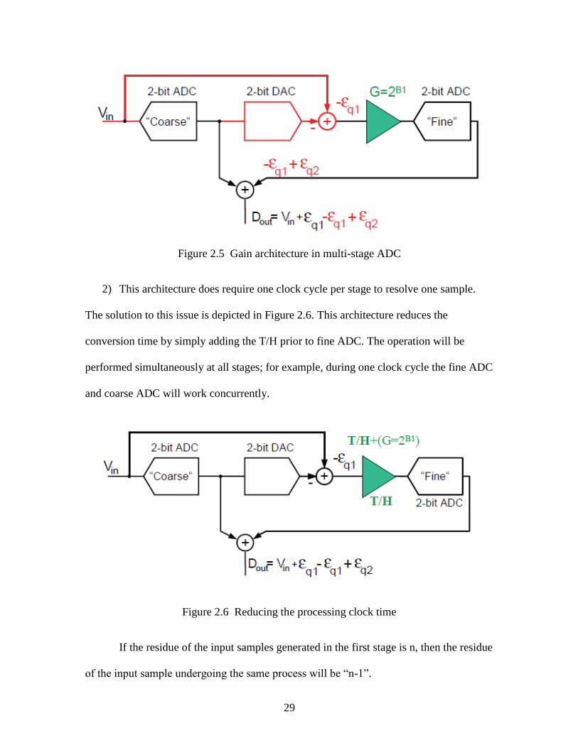
Figure 2.5 Gain architecture in multi-stage ADC
2) This architecture does require one clock cycle per stage to resolve one sample.
The solution to this issue is depicted in Figure 2.6. This architecture reduces the
conversion time by simply adding the T/H prior to fine ADC. The operation will be
performed simultaneously at all stages; for example, during one clock cycle the fine ADC
and coarse ADC will work concurrently.
Figure 2.6 Reducing the processing clock time
If the residue of the input samples generated in the first stage is n, then the residue
of the input sample undergoing the same process will be “n-1”.

30
Concurrent Stage Operation:
As shown in Figure 2.7, each stage performs the operation on an input sample and
gives the output to the following sampler. The sampler thus acquires the data and starts
performing the same operation repeatedly on different samples that are being
continuously fed to it. In this way, at any given point in time, all stages are processing
different samples concurrently. The throughput rate depends only on the speed of each
stage and the acquisition time of the next sampler.
(a)
(b)
Figure 2.7 (a) Pipeline multistage architecture (b) Pipeline architecture
Data Alignment:
In pipeline architecture, the digital output bits are obtained from each stage at
different points in time. These bits correspond to the same input sample and are made to

31
time-align with digital shift registers before being fed to the digital-error-correction logic,
as illustrated in Figure 2.8.
Figure 2.8 Digital correction logic
Data Latency:
In the pipelined architecture each sample must propagate through the entire
pipeline before all its associated bits are available for combining in the digital-error-
correction logic. Data latency is associated with pipelined ADC and is defined as the time
taken by the input voltage at the ADC to appear at the digital output of the pipelined
ADC. In Figure 2.9, the data latency is approximately a three-clock cycle.

32
Figure 2.9 Data latency concept
Pipeline ADC Characteristics:
Advantages:
1. Each stage has separate track-and-hold (T/H) amplifiers, which enable the
previous T/H to process the next incoming sample; this helps in simultaneous conversion
of multiple samples at different stages of the pipeline.
2. Pipelined ADCs have lower power consumption, lower cost and higher speed.
3. The extra bits will optimize correction of overlapping errors at each stage.
4. The number of stages grows linearly with resolution.
5. Non-Idealities can be removed from the analog circuits by using the pipeline.
6. Pipelined ADCs are highly versatile for 8 to16 bits, and from 1 to 200 MS/s.
Disadvantages:
1. It becomes difficult to understand the circuit, making biasing problematic.
2. The high number of stages results in pipelining latency.

33
3. Accurate timing is required for synchronized output.
4. Nonlinearities exist in gain and offset.
5. In control systems, latency due to pipelining may result in problems.
6. Throughput is limited by the speed of one stage.
Pipelined ADC V/S Flash ADC:
Unlike the parallel architecture of pipelined ADCs, there are a large number of
comparators in Flash ADCs architecture, which make them extremely fast. The number
of comparators increases by a factor of 2 for every extra bit of resolution. However, in the
case of a pipeline ADC, the complexity increases linearly rather than exponentially up to
the first order. Pipeline ADC has lower power consumption than Flash ADC. Unlike the
pipelined ADC, the flash comparator is susceptible to meta-stability.
Single-stage Pipeline ADC model with ideal DAC:
The residue voltage is equal to the gain times the quantization error. Also, the
value of Dout is equal to the summation of Vin and the quantization error. Figure 2.10
illustrates the structure of one stage in a pipeline ADC, where D is the quantized output
of Vin ‒Vres.
Figure 2.10 Single-Stage Pipeline model

34
Pipeline ADC error model:
We know that there are multiple ADC, DAC and Gain blocks at all stages of a
pipelined ADC. These components have some types of non-idealities associated with
them, which cause errors in the overall performance of a pipeline ADC. Gain stage offset,
comparator offset, and DAC offset are important sources of error in a pipeline ADC. See
figure 2.11 for illustration.
Figure 2.11 Pipeline Structure model
Stage Implementation:
1. From Figure 2.12 it is clear that every stage requires at least one T/H circuit for
the sampling and storing of input voltage Vin. During the track mode of the circuit, the
data or residue from the previous stage is acquired as an input for the next stage, whereas
in hold mode the residue is computed for the next stage via sub-ADC and sub-DAC
decisions. Here the residue plot is given for a 2-bit ADC. The gain is assumed to be 4.
The red is plotted for quantization error while the green is plotted for gain error. The
quantization error varies from -1/2 LSB to +1/2 LSB.

35
Figure 2.12 Overall architecture of ADC
2. In Figure 2.13, we have shown that T/H should not be placed in the beginning but
rather just before the sub-ADC. A second T/H should be placed just before the adder, as
shown i.e. T/H should be included implicitly in the stage-building block.
Figure 2.13 Improved T/H in Pipeline ADC

36
3. From Figure 2.14, we conclude that a single-switch capacitor circuit, which we
call MDAC the DAC, can replace both the gain and adder-subtractor stage. The sub-ADC
used here is a flash ADC along with a T/H circuit.
Figure 2.14 Alternative to gain and DAC stage in Pipeline
1.5-bit Stage Implementation:
Figure 2.15 is a schematic representation of a 1.5-bit stage implementation. We
have used two comparators in a sub-ADC block, which are attached to the latch. For the
DAC sub-block we have used a multiplexer. The input-to-select line of mux comes from
the latch output. In a gain-stage sub-block we have used the comparator with a grounded
non-inverting terminal. The inverting terminal is connected to the capacitor circuits, in
which Cf and Cs are connected parallel to each other. Cf will act as a sampling cap
during the acquisition mode of the device and as a feedback cap during the redistribution
cycle. The feedback factor is improved in this stage implementation.

37
Figure 2.15 Pipeline architecture at 1.5 bit stage
Minimum-stage resolution is advantageous for very high-speed analog to digital
converters because it minimizes the inter-stage gain and thus increases the bandwidth. A
1.5-bit stage is a 1-bit stage provided with some redundancy in order to achieve greater
tolerance. Later, the digital error correction method can be used to remove redundancy.
The 1.5 stage incorporates two symmetrical analog levels: VH and VL. The amplifier has
a gain of 2.
Since the gain is assumed to be 2, the VH and VL are assumed to lie within the
range of –Vref/2 to +Vref/2. There is no analog decision level at midrange in a 1.5 bit
configuration. The operating voltage range is divided into three categories: high, medium
and low. This stage has low-resolution ADC comprised of two comparators and some
simple encoding. The ADC output consists of two bits, B1 and B0. This is the digital
output before code conversion. For the Vin in the low, medium and high input ranges, the
respective codes are 00, 01, and 10. The DAC outputs are +Vref, 0, and -Vref for high,
medium and low input voltage, respectively.
38
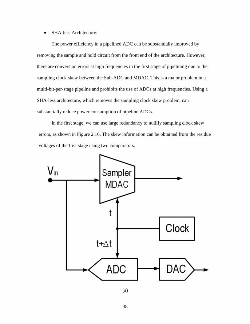
SHA-less Architecture:
The power efficiency in a pipelined ADC can be substantially improved by
removing the sample and hold circuit from the front end of the architecture. However,
there are conversion errors at high frequencies in the first stage of pipelining due to the
sampling clock skew between the Sub-ADC and MDAC. This is a major problem in a
multi-bit-per-stage pipeline and prohibits the use of ADCs at high frequencies. Using a
SHA-less architecture, which removes the sampling clock skew problem, can
substantially reduce power consumption of pipeline ADCs.
In the first stage, we can use large redundancy to nullify sampling clock skew
errors, as shown in Figure 2.16. The skew information can be obtained from the residue
voltages of the first stage using two comparators.
(a)

39
(b)
Figure 2.16 (a) ADC architecture with SHA (b) ADC architecture without SHA
Cascading Additional Stages:
Three main factors must be taken into consideration when cascading additional
stages in a design (see figure 2.17):
1. Final stage LSB will become very small.
2. It will be difficult to produce different Vref for different stages at the same time.
3. Full precision is necessary at all stages.

40
Figure 2.17 Suggestion for cascading additional stages
SAR ADC
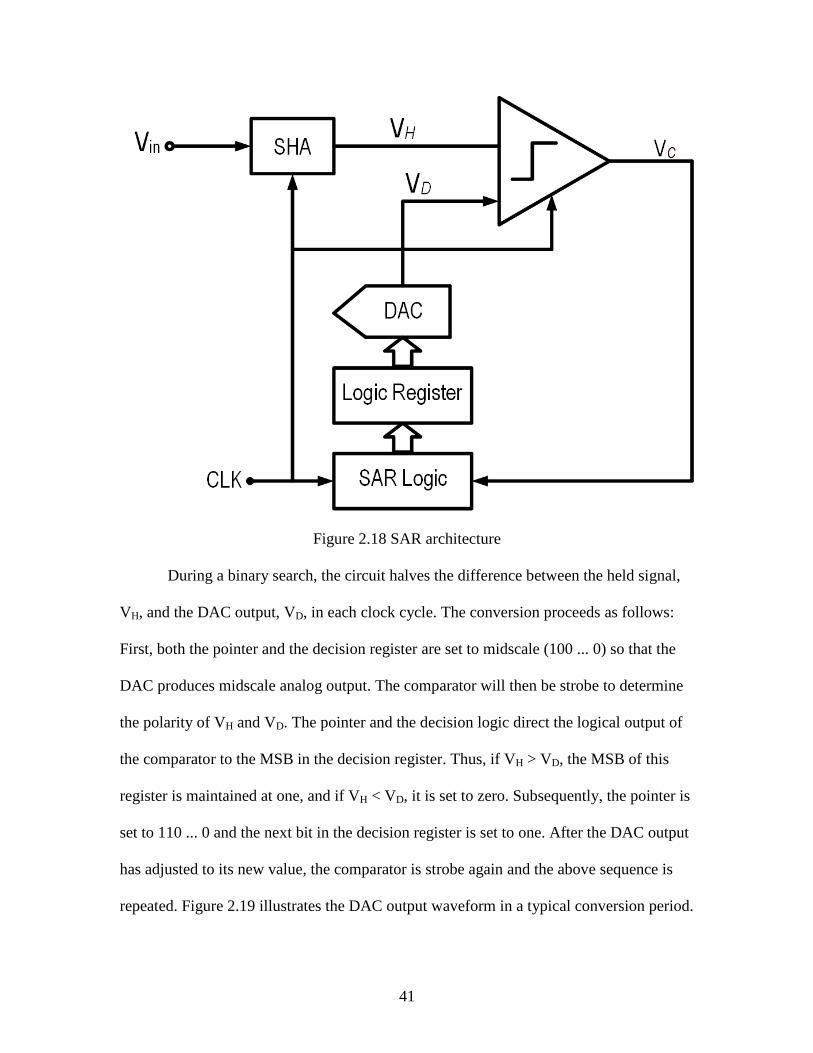
Successive approximation employs a "binary search" algorithm in a feedback
loop, which includes a l-bit AID converter. Figure 2.18 illustrates this architecture, which
consists of a front-end SHA, a comparator, a pointer (shift register), decision logic, a
decision register, and a DAC. The pointer indicates the last bit changed in the decision
register, and the data stored in this register is the result of all the comparisons performed
in the present conversion period.
41
Figure 2.18 SAR architecture
During a binary search, the circuit halves the difference between the held signal,
VH, and the DAC output, VD, in each clock cycle. The conversion proceeds as follows:
First, both the pointer and the decision register are set to midscale (100 ... 0) so that the
DAC produces midscale analog output. The comparator will then be strobe to determine
the polarity of VH and VD. The pointer and the decision logic direct the logical output of
the comparator to the MSB in the decision register. Thus, if VH > VD, the MSB of this
register is maintained at one, and if VH < VD, it is set to zero. Subsequently, the pointer is
set to 110 ... 0 and the next bit in the decision register is set to one. After the DAC output
has adjusted to its new value, the comparator is strobe again and the above sequence is
repeated. Figure 2.19 illustrates the DAC output waveform in a typical conversion period.

42
Figure 2.19 DAC output waveform for a typical VH input
For a resolution of M bits, the successive approximation architecture is at least M
times slower than full-flash configurations, but offers several advantages. First, note that
the comparator offset voltage does not affect the linearity of the overall converter because
it can be represented as a voltage source in series with the SHA output, indicating that the
offset voltage simply adds to the analog input and hence appears as an offset in the
overall characteristics. Consequently, the comparator can be designed for high-speed
operation even in high-resolution systems. Of course, the input EMS noise of the
comparator must be much lower than 1 LSB. Second, this architecture does not require an
explicit subtractor, an important advantage in high-resolution applications. Finally, the
circuit complexity and power dissipation are in general lower than that of other
architectures.

43
If the front-end SHA provides the required linearity and speed, and the
comparator input-referred noise is low enough, the converter's performance depends
primarily on that of the DAC. In particular, the differential and integral nonlinearity of
the converter are indicated by those of the DAC, and the maximum conversion rate is
limited by its output settling time. Note that in the first conversion cycle, the DAC output
must settle to maximum resolution of the system in order for the comparator to correctly
determine the MSB. Thus, if the clock period is constant, the conversion cycles which
follow will be as long as the first one, implying that the conversion rate is constrained by
the speed of the DAC.
Successive approximation converters that incorporate capacitor DACs are usually
based on the "charge redistribution" principle [1]. We illustrate this principle using the
simplified diagram in Figure 2.22, where the DAC consists of binary-weighted capacitors
( ) and [1]. In the sampling mode, the top plate
is grounded, while all the bottom plates are connected to the input signal. In the transition
from the sampling mode to the hold/conversion mode, Sp turns off and all the bottom
plates are grounded, causing the top plate voltage to be equal to the negative of the
sampled level. The conversion then proceeds by switching the bottom plate of some of
the CJ-Cu to VREF (according to a binary search algorithm) such that the top plate voltage
eventually returns to zero. For example, to evaluate the MSB, the bottom plate of is
switched from ground to VREF so that the top plate voltage increases by VREF/2.
Subsequently, the comparator is strobe to determine the polarity of the difference
between the top plate voltage and ground, and hence the MSB. The following steps are
similar to those described for Figure 2.18.

44
The circuit in Figure 2.20 has several interesting features. Here the D/A converter
operates as a sample-and-hold circuit, the capacitor array acts as the storage element, and
while the top and bottom plate switch controls the sampling. The accuracy/speed trade-
off described for MOS switches is considerably relaxed here because Sp, which always
turns off with its source, performs the sample-to-hold transition and drain at ground
potential, injecting a constant charge onto the array.
Figure 2.20 Charge redistribution architecture
Another feature of this configuration is that at the end of the conversion, the top
plate potential is very close to zero. This in turn means that the junction capacitance of s
contributes very little nonlinearity to the system [1]. Note that since during sampling Sp is
in series with the entire array, it must have a low on-resistance and hence a large width so
as to provide fast acquisition. Consequently, its junction capacitance is usually
comparable with the value of the smallest capacitor in the array. Also, because the
comparator eventually compares VD with the ground potential, it need not maintain a
high precision across a wide input common-mode range, an important feature in low-

45
voltage designs. Nonetheless, the comparator must have a fast overdrive recovery, i.e.,
must not slow down after it has sensed a large differential input.
In the case of high resolutions, the ratio of the largest and the smallest capacitors
(2m-1
), as well as the total value of the array capacitance, may be excessively large. For
example, in a 12-bit converter, the ratio of the MSB to the LSB capacitors is equal to
2048, and the array comprises 4096 equal unit capacitors. As the minimum size of the
smallest capacitor is often dictated by uniformity and matching considerations, the area
and capacitance of such an array may be very large, thus yielding an enormous input
capacitance for the converter, slowing down the preceding circuit and complicating the
routing. Additionally, the large capacitance of the array draws large current spikes from
the ground and VREF lines during transients, causing ringing and long settling times in the
presence of inductance in series with these lines.
In order to alleviate these problems, the ratio of the largest to the smallest
capacitors in the array must be decreased. For example, rather than scaling all the
capacitors, their bottom plate voltage swings can be scaled. This can be accomplished by
combining a resistor ladder with the capacitor array such that the ladder provides
fractions of VREF [2]. Figure 2.21 shows an example of the resistor ladder generating
VREF/2, lowering the maximum ratio required for the capacitors in the array by a factor of
2. Note that the matching of the ladder's resistors is not critical if used for only a few
LSBs.

46
Figure 2.21 Example of DAC architecture
A number of successive approximation AID converters have been realized in
bipolar, CMOS, and BiCMOS technologies [3, 4, 5]. The self-calibration capability and
the transistor density of CMOS and BiCMOS technologies have provided resolutions as
high as 18 bits [5].
Time-Interleaved (TI) Technique
In systems where ultimate speed is the primary goal, identical AID converters can
be interleaved so as to achieve more parallelism than simple flash topologies. Figure
2.22(a) shows an interleaved architecture where n sample-and-hold circuits are controlled
by CK1,…, CKn preceded in m-bit ADCs [6]. A multiplexer selects the digital output of
each ADC at the proper time, providing the output corresponding to each sample. Note
that ADCi, ... , ADCn can employ any architecture, but full flash is most commonly used
to allow a high conversion rate.
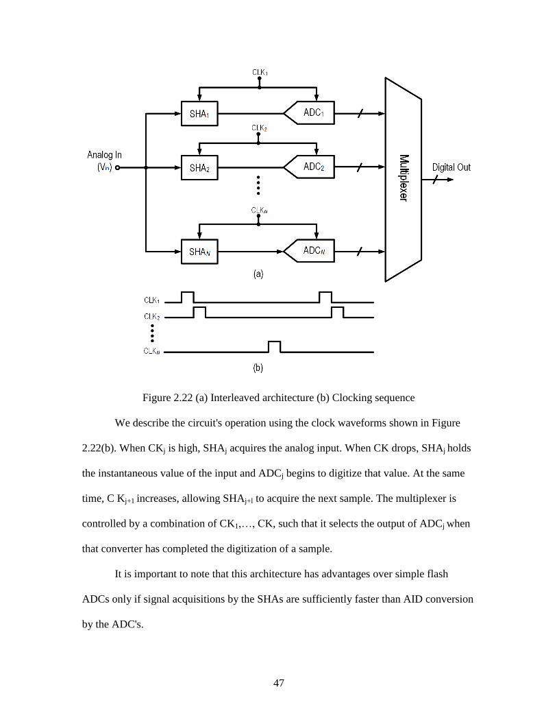
47
Figure 2.22 (a) Interleaved architecture (b) Clocking sequence
We describe the circuit's operation using the clock waveforms shown in Figure
2.22(b). When CKj is high, SHAj acquires the analog input. When CK drops, SHAj holds
the instantaneous value of the input and ADCj begins to digitize that value. At the same
time, C Kj+1 increases, allowing SHAj+l to acquire the next sample. The multiplexer is
controlled by a combination of CK1,…, CK, such that it selects the output of ADCj when
that converter has completed the digitization of a sample.
It is important to note that this architecture has advantages over simple flash
ADCs only if signal acquisitions by the SHAs are sufficiently faster than AID conversion
by the ADC's.

48
While they produce high conversion rates, interleaved architectures suffer from
accuracy degradation due to parameter mismatches among their constituent sampling
circuits and AID converters. In particular, mismatches in gain, differential and integral
nonlinearity, timing, and offset give rise to higher noise in the overall output. The effects
of these errors in time and frequency domains have been analyzed extensively [6, 7, 8].
The potential of interleaved architectures has been demonstrated in various
ADCs, the most recent case being in an 8-bit 8-GHz system designed for real-time
sampling of signals in a digital oscilloscope [9]. The system employs a total of sixteen
500-MHz bipolar flash ADCs along with a sample-and-filter technique that relaxes the
bandwidths required in the preceding sampling circuits. In CMOS technology, an 8-bit
85-MHz ADC using four interleaved converters has been reported [10].
Hybrid Architectures
Hybrid ADCs are those architectures that result from the combination of various
others, such as a converter that is a mix of a Sigma-Delta (∑∆) and a pipelined ADC [11].
Another example is a mix of an SAR and a pipelined ADC [12]. Yet another variation is
one that implements the binary search principle of an SAR ADC as part of a two-step
converter [13].
Hybrid architectures are often the result of the designer’s intent to combine the
strengths of different types of ADCs and actually create an architecture that, at least for a
given set of specifications, is better overall than any one of its components.
For instance, ∑∆ ADCs tend to be more suitable for higher resolution and lower
signal band than pipelined ADCs, which, in turn, are well suited for wideband inputs but
are usually a better fit to moderate resolution. Combining a ∑∆ front end with a pipelined

49
ADC back end was the driving idea for the 16-bit cascaded (MASH) hybrid ADC
discussed in [11] to obtain high resolution (89 dB SNR) and high speed (1.25 MHz input
bandwidth), even after 15 years without requiring calibration.
The block diagram of this cascaded (MASH) converter is shown in Figure 2.23.
Here a first-stage k-bit ∑∆ modulator is cascaded with a high-resolution m-bit second
stage. This is similar to a Leslie–Singh [14] architecture where only some of the
quantized bits are fed back to the input of the modulator. The second-stage ADC provides
m-bits at the same rate as the ∑∆ modulator’s quantizer. In this structure, since the m-bit
quantizer is not closed in a loop, any associated latency is unimportant. The D-cycle
delay z−D is used to equalize the ∑∆ modulator output with the m-bit quantizer output,
which is in fact implemented using a pipelined ADC (hence having latency).
Figure 2.23 A cascaded hybrid ∑∆ ADC architecture
Careful selection of the architecture and parameters in this hybrid improves
performance: a 12-bit pipeline ADC does not require calibration, as the combination of a

50
MASH structure and a multi-bit loop in the front-end ∑∆ allows the use of a limited
OSR. Overall, the converter had a 16-bit resolution and achieved 89 dB SNR in a
bandwidth of 1.25 MHz. It consumed 550 mW and was implemented on a 0.6 μm CMOS
technology with dual 5AVdd and 3DVdd supplies.
Oversampling ADC
Oversampling ∑∆ ADCs [15, 16] are based on the principle that conversion error
can be high-pass filtered and later removed by digital filters. Requirements on the analog
parts are lenient and high resolutions can be achieved. The drawback of this type of
converter is that for high resolutions the signal bandwidth is narrow due to the
oversampling. A second-order ∑∆ modulator is shown in Figure 2.24. The modulator
consists of two discrete-time integrators, two DACs, and one quantizer. If the
quantization error is modeled as white noise, the output signal is given by E(z) as
quantization noise in the quantizer and X(z) is the input signal.
Figure 2.24 A second-order sigma-delta modulator
The quantization noise is high-pass filtered while the input signal is only delayed.
Removing the high frequency noise with digital filters and decimating the signal,
achieves an output signal with a minimum quantization noise. Every doubling of the
sampling rate will provide L + 0.5 extra bits, where L is the order of the modulator.

51
To increase the resolution, the order of the modulator or the resolution of the
quantizer must be increased. A problem with increasing the resolution of the quantizer is
that nonlinearities in the DACs will directly limit the resolution of the ADC. A DAC with
only two output levels will have only offset and gain errors, while multi-bit DACs also
produce non-linearity.
There are also problems involved when increasing the order of a single-stage
modulator. Special architectures to avoid instability must be employed and a low input
swing may be required to avoid saturation of the modulator. This may necessitate large
capacitors and a large capacitance during implementation, which would reduce the speed
[17]. By using a multi-stage structure these problems are avoided, but sensitivity to
matching errors between the analog and digital parts limits the resolution.
Some alternatives exist to increase the bandwidth. A 16-bit converter with an
oversampling ratio of only 8 was designed [18] by combining a sigma-delta modulator
with a pipelined converter. A multi-bit quantizer and dynamic element matching help
reduce distortion caused by the DAC.
Sigma-Delta ADC
Delta modulation requires two integrators for the modulation and demodulation
processes, as shown in Figure 2.25(a). Since integration is a linear operation, the second
integrator can be moved before the modulator without altering the overall input/output
characteristics. Furthermore, the two integrators in Figure 2.25 can be combined into a
single integrator by the linear operation property.

52
Figure 2.25 Derivation of Sigma-Delta modulation from delta modulation (modified from
[19])
The arrangement shown in Figure 2.26 is called a sigma-delta (Σ∆) modulator
[19]. This structure, besides being simpler, can be considered as a “smoothed version” of
a 1-bit delta modulator.
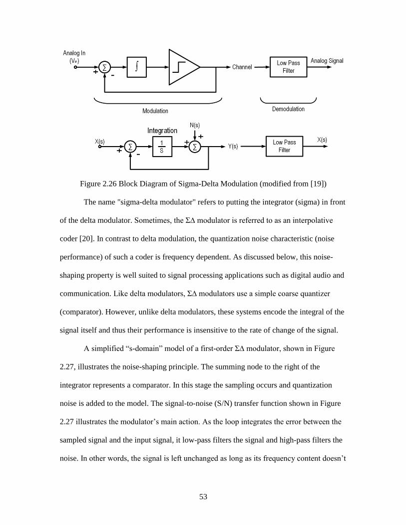
53
Figure 2.26 Block Diagram of Sigma-Delta Modulation (modified from [19])
The name "sigma-delta modulator" refers to putting the integrator (sigma) in front
of the delta modulator. Sometimes, the Σ∆ modulator is referred to as an interpolative
coder [20]. In contrast to delta modulation, the quantization noise characteristic (noise
performance) of such a coder is frequency dependent. As discussed below, this noise-
shaping property is well suited to signal processing applications such as digital audio and
communication. Like delta modulators, Σ∆ modulators use a simple coarse quantizer
(comparator). However, unlike delta modulators, these systems encode the integral of the
signal itself and thus their performance is insensitive to the rate of change of the signal.
A simplified “s-domain” model of a first-order Σ∆ modulator, shown in Figure
2.27, illustrates the noise-shaping principle. The summing node to the right of the
integrator represents a comparator. In this stage the sampling occurs and quantization
noise is added to the model. The signal-to-noise (S/N) transfer function shown in Figure
2.27 illustrates the modulator’s main action. As the loop integrates the error between the
sampled signal and the input signal, it low-pass filters the signal and high-pass filters the
noise. In other words, the signal is left unchanged as long as its frequency content doesn’t
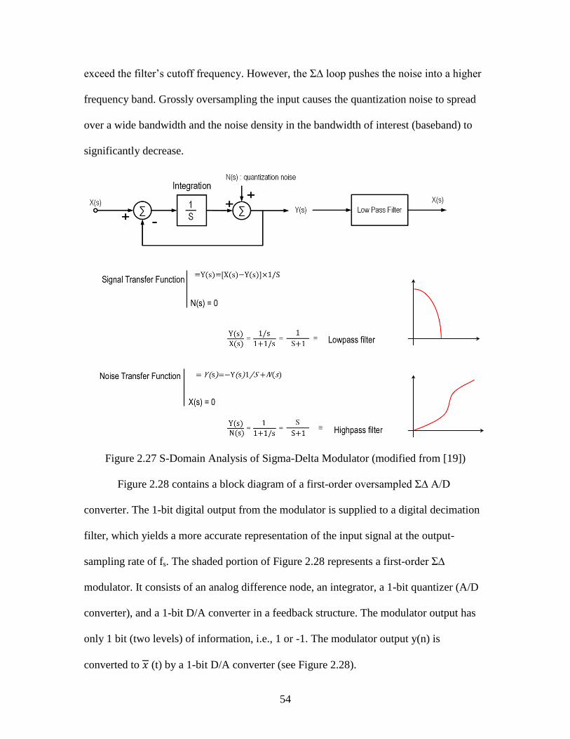
54
exceed the filter’s cutoff frequency. However, the Σ∆ loop pushes the noise into a higher
frequency band. Grossly oversampling the input causes the quantization noise to spread
over a wide bandwidth and the noise density in the bandwidth of interest (baseband) to
significantly decrease.
Figure 2.27 S-Domain Analysis of Sigma-Delta Modulator (modified from [19])
Figure 2.28 contains a block diagram of a first-order oversampled Σ∆ A/D
converter. The 1-bit digital output from the modulator is supplied to a digital decimation
filter, which yields a more accurate representation of the input signal at the output-
sampling rate of fs. The shaded portion of Figure 2.28 represents a first-order Σ∆
modulator. It consists of an analog difference node, an integrator, a 1-bit quantizer (A/D
converter), and a 1-bit D/A converter in a feedback structure. The modulator output has
only 1 bit (two levels) of information, i.e., 1 or -1. The modulator output y(n) is
converted to (t) by a 1-bit D/A converter (see Figure 2.28).
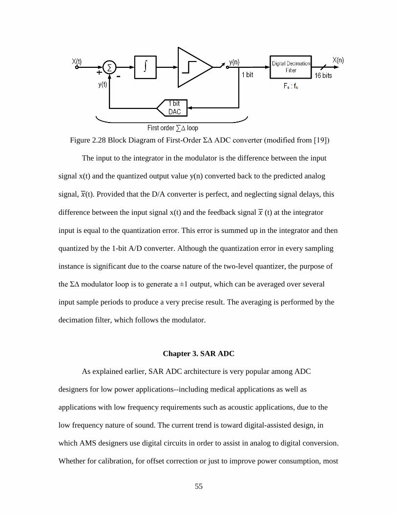
55
Figure 2.28 Block Diagram of First-Order Σ∆ ADC converter (modified from [19])
The input to the integrator in the modulator is the difference between the input
signal x(t) and the quantized output value y(n) converted back to the predicted analog
signal, (t). Provided that the D/A converter is perfect, and neglecting signal delays, this
difference between the input signal x(t) and the feedback signal (t) at the integrator
input is equal to the quantization error. This error is summed up in the integrator and then
quantized by the 1-bit A/D converter. Although the quantization error in every sampling
instance is significant due to the coarse nature of the two-level quantizer, the purpose of
the Σ∆ modulator loop is to generate a ±1 output, which can be averaged over several
input sample periods to produce a very precise result. The averaging is performed by the
decimation filter, which follows the modulator.
Chapter 3. SAR ADC
As explained earlier, SAR ADC architecture is very popular among ADC
designers for low power applications--including medical applications as well as
applications with low frequency requirements such as acoustic applications, due to the
low frequency nature of sound. The current trend is toward digital-assisted design, in
which AMS designers use digital circuits in order to assist in analog to digital conversion.
Whether for calibration, for offset correction or just to improve power consumption, most

56
designers prefer to use digital-assisted circuits in ADC design. SAR ADC is the only
architecture that employs a digital circuit in its architecture, a crucial part of the SAR
ADC. SAR logic determines the value for reference generation in DAC and also
generates the final digital value in the output.
SAR ADC Architecture
SAR ADC has a very simple architecture. Its single comparator block is relatively
low power consuming. It also reduces the power-hungry requirements of most ADC
architectures by not having an Op-amp block in its system, and hence an appreciable
power consumption factor can be achieved in comparison with other architectures. The
other main block is the SAR Logic, whose function is to take the output of the
comparator into account in generating binary weighted references for DAC. All various
DAC architectures perform the same operation in SAR ADC, which is to generate the
appropriate reference voltage for the comparator.
The SAR architecture used in this project is a single-input comparator with a
switch capacitor DAC. In this form of architecture, there is only one input to the
comparator, and only one set of capacitors in the switched capacitor DAC to generate the
required reference levels.
SAR logic is design at the RTL level with Verilog code. The logic will decide the
appropriate DAC input for reference-level generation. Figure 3.1 shows the employed
architecture.

57
Figure 3.1 SAR architecture
SAR ADC Operation
SAR ADC operates on two different clock frequencies. The first is the sampling
frequency and the second is the operating frequency of the comparator. After the
sampling clock samples and quantifies the analog signal in the sampler block, the
comparator makes decisions based on the input values from the DAC and sampler. The
frequency at which the comparator and DAC operate depends on the number of bits the
ADC is designed for. If the ADC has N bits, the operating frequency of the comparator,
DAC, and SAR logic is (2×N) times the sampling frequency. The reason for this speed
discrepancy is that, for an N-bit SAR ADC, the SAR logic requires N decisions in order
to generate the final digital value. The entire decision-making process happens in the hold
time of the sampling frequency, which means that the overall frequency of the
comparator clock would be twice the number of bits times the sampling frequency.
(3.1)
At the beginning of the hold time, the SAR logic generates the binary value MSB
and feeds it to the DAC. In this way, at the very beginning of the hold time a reference
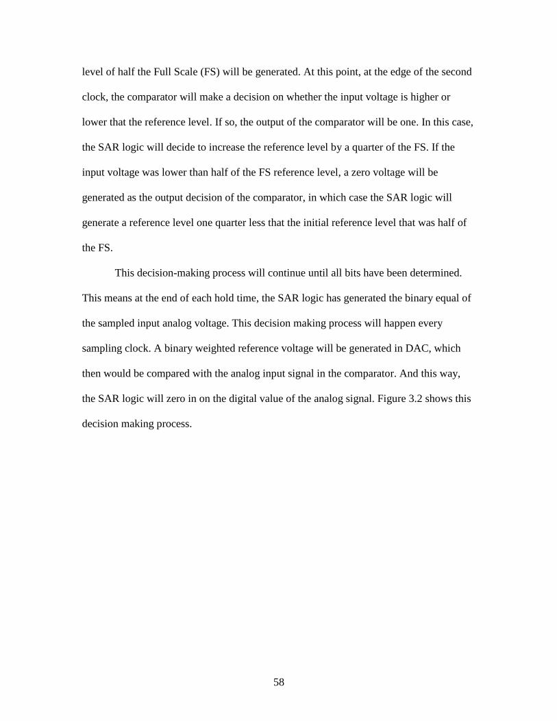
58
level of half the Full Scale (FS) will be generated. At this point, at the edge of the second
clock, the comparator will make a decision on whether the input voltage is higher or
lower that the reference level. If so, the output of the comparator will be one. In this case,
the SAR logic will decide to increase the reference level by a quarter of the FS. If the
input voltage was lower than half of the FS reference level, a zero voltage will be
generated as the output decision of the comparator, in which case the SAR logic will
generate a reference level one quarter less that the initial reference level that was half of
the FS.
This decision-making process will continue until all bits have been determined.
This means at the end of each hold time, the SAR logic has generated the binary equal of
the sampled input analog voltage. This decision making process will happen every
sampling clock. A binary weighted reference voltage will be generated in DAC, which
then would be compared with the analog input signal in the comparator. And this way,
the SAR logic will zero in on the digital value of the analog signal. Figure 3.2 shows this
decision making process.

59
Figure 3.2 SAR decision-making process
SAR Logic
The SAR logic plays a crucial role in SAR ADC system. It generated the binary
weighted decision for appropriate reference levels in DAC and at the end of operation
will give the final binary value of the analog signal to the output of the ADC system.
SAR logic is usually designed with hardware description language (HDL). However, for
high-speed applications, designers may prefer to design costume SAR logic in high-speed
CMOS logics.
The basic operation of SAR logic is fairly simple. It will generate an N-bit output
where N is the number of ADC bits. This output will be generated based on the output of
the comparator, with the exception of the first clock, which is always 1 for the highest bit
and zero for the remainder of the bits.
The second decision will be made based on the decision of the comparator for the
first reference level that was generated by the comparison of the input signal and half FS.

60
An input of one from the comparator will always result in holding the previous code
while generating another for the next bit.
A decision of zero from the comparator will result in a shift to the right of the
binary weighted code in the SAR logic output. This means the previous bit, which was
one in the previous clock, would become zero and the next lower value bit will become
one.
In this process, during every clock cycle, the logic will shift the output bit to the
right, that is, to a lower value bit. The only difference is in the comparator output, in
whether the SAR logic will hold the previous bit as one or change it back to zero.
SAR DAC
The SAR DAC is the block where the reference level for comparator decision-
making is generated. The most significant DAC architecture is the resistive ladder with
current sources and switched capacitors. Each of these architectures has its advantages
and disadvantages.
The resistive ladder DAC is extremely fast and settles quickly. However, the
power consumption for resistive DAC is very high. Also, the process variation has
significant effects on the value of resistors, which may lead to some errors in DAC
reference generation. Figure 3.3 is an illustration of resistive DAC architecture.

61
Figure 3. 3 Resistive DAC architecture
On the other hand, switched capacitor DAC consumes very little power but the
settling time is higher, which is why it is challenging to design switched capacitor DAC
circuits for high-speed ADC applications. Moreover, the capacitive load on the
comparator input would greatly affect the comparator offset and speed. Figure 3.4 depicts
switched capacitor DAC architecture.
Figure 3.4 Switched capacitor DAC architecture

62
However, as already mentioned, the switched capacitor is very power efficient,
and due to the nature of SAR ADC, low power consumption is the main goal for the
ADC, not lower speed. For this, the switched capacitor DAC is ideal.
Chapter 4. Proposed SAR ADC Design
In this chapter we will present the proposed design for the SAR ADC. The
architecture of the proposed SAR ADC will be presented, as well as the design of each
block. We will discuss the design and operation of each block.
The proposed SAR architecture is based on the unique architecture of the
comparator. Therefore, all the other blocks have been designed around the architecture
and requirements of the novel comparator. Figure 4.1 shows the architecture of the SAR
ADC in the test bench.
Figure 4.1 Designed SAR ADC architecture
The proposed comparator has a single-input design. Therefore, the DAC circuit
for this comparator had to be a single-input/single-output DAC. The single-input DAC
poses some unique challenges.

63
The SAR logic was designed with Verilog HDL language to generate the binary
weighted references.
We have designed an 8-bit SAR ADC, in which the proposed sampling frequency
is 500 KHz. Although signal frequencies for medical purposes are much lower than 500
KHz, a higher sampling frequency capability would generate higher resolution and more
accurate digital values for the analog input.
The input clock frequency at which the comparator, DAC, and SAR logic operate
is 16 times higher than the sampling frequency. This means that the comparator operates
at 8 MHz, a very impressive operating frequency given the proposed architecture of the
comparator.
State of the Art in Proposed Design
The state of the art in this project is the unique and novel architecture of the
proposed comparator. To my best knowledge, the proposed architecture for the
comparator used in this SAR ADC is unique. This architecture is bulk-driven and cross-
coupled and resulted in a comparison operation for the circuit, whereas in a conventional
circuit, the analog input signal is fed to the gate of the MOS transistors. In some
situations, the input signal is fed into the source or drain of the MOS transistor, but these
architectures are not used in the comparator design.
In recent years, the process of feeding the input signal into the bulk of the
transistor and using bulk-driven transistors in sub-threshold sensing and amplification has
gained some attention. Bulk-driven architecture has rarely been used in comparator
architecture, and certainly not in a cross-coupled architecture.
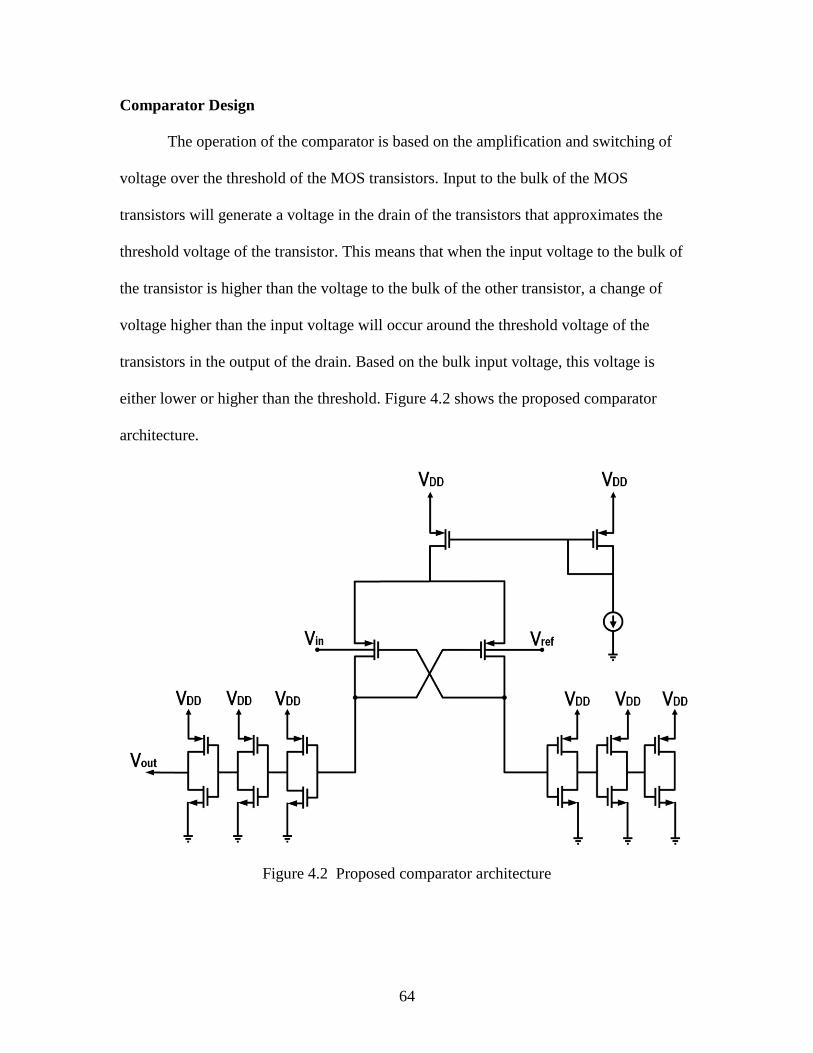
64
Comparator Design
The operation of the comparator is based on the amplification and switching of
voltage over the threshold of the MOS transistors. Input to the bulk of the MOS
transistors will generate a voltage in the drain of the transistors that approximates the
threshold voltage of the transistor. This means that when the input voltage to the bulk of
the transistor is higher than the voltage to the bulk of the other transistor, a change of
voltage higher than the input voltage will occur around the threshold voltage of the
transistors in the output of the drain. Based on the bulk input voltage, this voltage is
either lower or higher than the threshold. Figure 4.2 shows the proposed comparator
architecture.
Figure 4.2 Proposed comparator architecture

65
In this architecture, an input voltage higher than the reference voltage will
generate a voltage that is lower than the threshold. This lower voltage in the cross-
coupled configuration will turn on the other MOS transistor that is connected to the
reference voltage, allowing for a higher than threshold voltage to be generated which will
in turn try to switch the transistor off and generate a zero in the output. This swing of
voltages will settle at a point where the output node has a low value, and with a chain of
invertors we can easily generate the desired output of 1.
The reverse of this situation is where the input voltage is less than the reference
voltage, every operation that we explained will happen in reverse, and the final output
voltage will be high, with the chain of invertors generating the value of zero.
In this way, we were able to generate the switching operation required by the
comparator in one shot, combining two different architectures in one. The main
advantage of this architecture is low power consumption. Whereas the power
consumption for most comparators is in the range of milliwatts or at most microwatts,
this comparator has power consumption in the range of nanowatts.
Proposed DAC Design
Figure 4.3 shows the proposed architecture for the DAC designed in this ADC.
Figure 4.3 Designed DAC switch-cap architecture

66
This is a switched-capacitor DAC. The operation is arranged in such a way that
when the clock is present all the capacitors will be charged to the voltage value of the
input signal. And in the hold time for the clock, a secondary voltage will be applied to
some of the capacitors that are based on the desired binary weighted value of the
reference level. The switches are constructed with Transmission Gates (TG) and the
schematic for this switch is shown in figure 4.4 Design and sizing of each switch is based
on the size of the capacitor. As the capacitor sizes in the DAC increase by the order of
two, so should the sizes of the switches.
Figure 4.4 Architecture for the internal switches used in DAC
At this point, the overall value that will be generated is based on the preservation
of charge law. This law states that the charges stored in capacitors will not dissipate but
rather will be evenly distributed and will generate a final value at the output. The
following formula shows the operation of the switched capacitor DAC.

67
(4.1)
(4.2)
The size of DAC capacitors increases progressively, based on the order of 2. This
means that the first bit will be connected to the DAC with a size of C and the next bit will
be connected to a capacitor with a size of 2×C. This is how a binary weighted reference is
generated, where a combination of the charges based on the sizes of capacitors will
generate the overall reference voltage.
Based on this operation, the output of the DAC is connected to the negative node
of the comparator.
SAR Logic Design in Verilog
The SAR logic operation has been explained. The code for the SAR logic block in
Verilog language is as follows:
//Verilog HDL for "SAR_ADC", "SAR_Logic" "verilog"
module SAR_logic ( counter, comp_decision, set, clk );
parameter nbits = 8; // number of bits in the ADC
input comp_decision; // output of the comparator (discrete)
input set; // positive edge conversion activation (if no conversion is
running)
input clk; // the sampling frequency 500 KHz clock

68
output [nbits-1:0] counter; //the output to the DAC
reg [nbits-1:0] counter;
reg status;
integer i;
initial begin
status = 0;
end
//-----------8 bit binary weight Counter----------------
always @(posedge set) begin
counter[nbits-1:0] = 8'b10000000;
for(i = nbits-1 ; i >= 0 ; i = i-1 )
begin
@(posedge clk) begin
@(clk==1)
if(comp_decision == 1) begin
counter[i] = 1;
counter[i-1] = 1;
end
else begin

69
counter[i]=0;
counter[i-1] = 1;
//end
end
end
end
end
endmodule
Sample and Hold Design
The sample and hold architecture is one of the basic architectures that we have
used in this project. The design consists of a simple TG switch and a capacitor. Capacitor
and transistor sizes for the sampler were based on simulations in order to achieve the
fastest switching capability and best holding mode for the sampler. Figure 4.5 shows the
architecture for the sampler
Figure 4.5 Sampler architecture
70
Chapter 5. AMS Test Simulation and Results
In this chapter we present the test results for all the circuits and blocks in this
project. We will study each circuit separately and present the test bench and test results
for that circuit. All the simulations were done in Cadence Virtuoso. We used
Globalfoundries 45 nm CMOS technology for design and simulation in this project.
After all blocks were designed and tested separately, they were connected
together to form the final SAR ADC. At this point, due to the different nature of the
blocks, we had to run the final simulations in the AMS mode.
In order to run simulations in AMS mode, one must configure the Cadence setting
for mixed configuration mode. Firstly, we will present the configuration settings for AMS
mode in Cadence Virtuoso.
Setting AMS Configuration in Cadence
In order for Cadence to be able to run simulations between different blocks in
Virtuoso, the various blocks including Verilog, Verilog-a, and transistor level circuits
must first be connected to each other. For these different blocks to run as a whole, a
connection rule must be applied. In SJSU Cadence labs, a connection library is provided
to connect different blocks in Cadence. Therefore, the first step is adding the connection
library in the library path section.
connectLib Library
connectLib is an internal connection library for Cadence AMS simulators. This
library contains all the connection rules and configurations for different analog, digital,
and behavioral modes in Cadence. In order to add this library, one must first go to Tools
-> library path editor -> Add Library or just click on the last empty library path section

71
and add the library name and path. Figure 5.1 shows the library and path, which is the
same for all SJSU Cadence labs.
Figure 5.1 Library path for connectLib
Config view
After the connection rule library (connectLib) has been added, these
configurations can be used in AMS simulations. Next, we must open a new view mode
for the test bench. This new view mode is config view. We can do this by going to
Library Manager -> File -> New -> cell view, and then in the view mode selecting
config. Once the config mode is open, we can proceed to select AMS simulation.
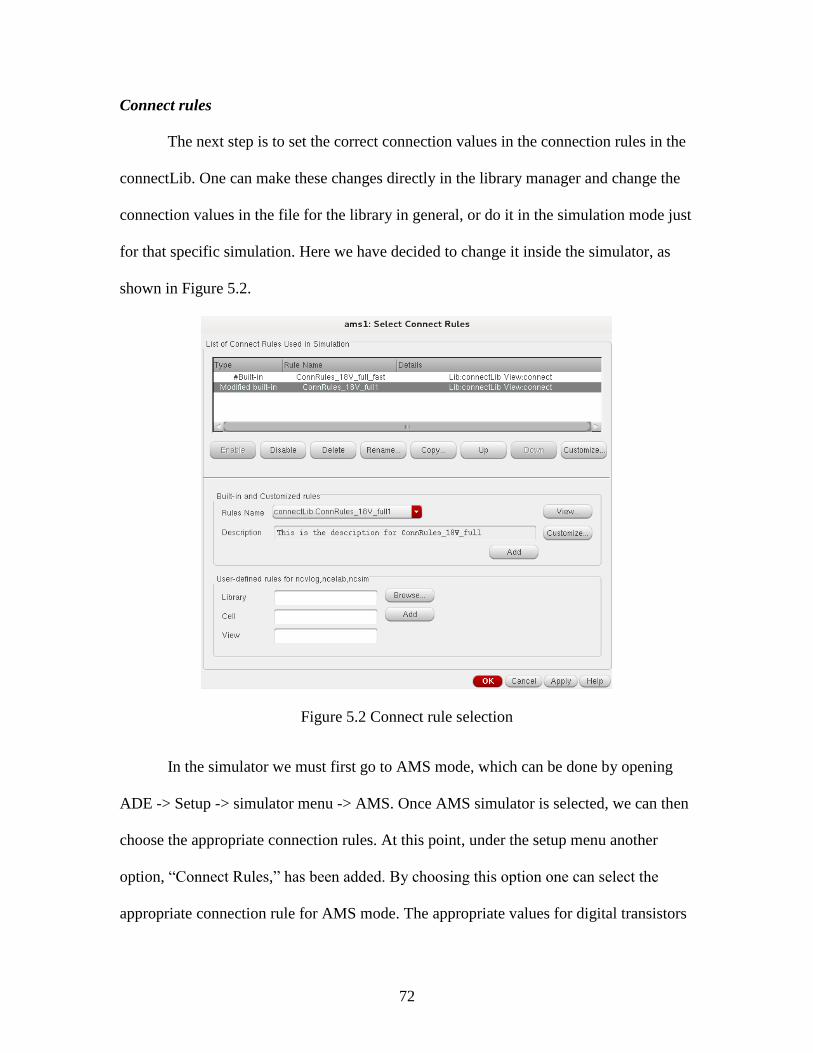
72
Connect rules
The next step is to set the correct connection values in the connection rules in the
connectLib. One can make these changes directly in the library manager and change the
connection values in the file for the library in general, or do it in the simulation mode just
for that specific simulation. Here we have decided to change it inside the simulator, as
shown in Figure 5.2.
Figure 5.2 Connect rule selection
In the simulator we must first go to AMS mode, which can be done by opening
ADE -> Setup -> simulator menu -> AMS. Once AMS simulator is selected, we can then
choose the appropriate connection rules. At this point, under the setup menu another
option, “Connect Rules,” has been added. By choosing this option one can select the
appropriate connection rule for AMS mode. The appropriate values for digital transistors

73
in Verilog block should be applied. We have done so based on our project’s needs, as
shown in Figure 5.3.
Figure 5.3 Setting the values for connect rules
Other settings, such as vddd and gndd, must be selected in the Verilog block in
order to use the general supply voltages for the digital blocks in the same as for analog
and transistor-level blocks.
Sampler Test Results
Figure 5.4 shows the test bench for the sampler block in the proposed SAR ADC.
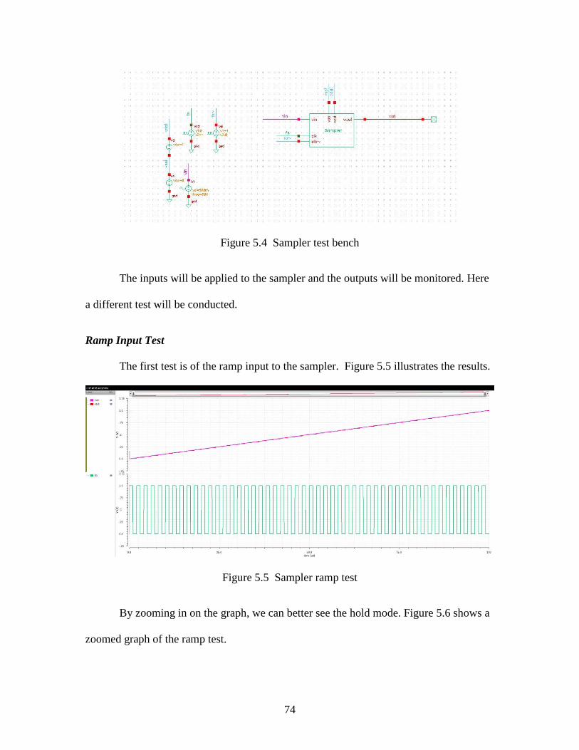
74
Figure 5.4 Sampler test bench
The inputs will be applied to the sampler and the outputs will be monitored. Here
a different test will be conducted.
Ramp Input Test
The first test is of the ramp input to the sampler. Figure 5.5 illustrates the results.
Figure 5.5 Sampler ramp test
By zooming in on the graph, we can better see the hold mode. Figure 5.6 shows a
zoomed graph of the ramp test.

75
Figure 5.6 Sampler ramp test (zoomed)
Sinusoidal Input Test
The next test is one of input voltage. This is a typical analog input in ADC
systems and we want to see how the sampler operates. Figure 5.7 shows the results.
Figure 5.7 Sampler sinusoidal input test
By zooming in the on graph we can get a better sense of the hold mode of the
sinusoidal input. See Figure 5.8.
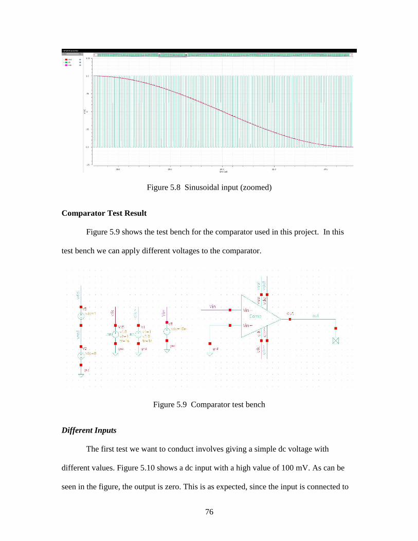
76
Figure 5.8 Sinusoidal input (zoomed)
Comparator Test Result
Figure 5.9 shows the test bench for the comparator used in this project. In this
test bench we can apply different voltages to the comparator.
Figure 5.9 Comparator test bench
Different Inputs
The first test we want to conduct involves giving a simple dc voltage with
different values. Figure 5.10 shows a dc input with a high value of 100 mV. As can be
seen in the figure, the output is zero. This is as expected, since the input is connected to

77
the negative port of the comparator. When the input voltage is higher than zero, the
output is zero, and when the input is less than zero, comparator output will be one.
Figure 5.10 Comparator test result
Now we will apply a negative input of the same magnitude and observe the
results. Figure 5.11 contains the comparator results.
Figure 5.11 Comparator test result
As seen in the figure, the comparator generates an output of one when the input is
less than zero. However, when the input value is very high, we must test the comparator

78
for lower values. We tried a lower voltage of 10 mV and -10 mV for the comparator.
Figure 5.12 shows the results.
Figure 5.12 Comparator test result
Figure 5.13 shows the comparator output decision for an input voltage of -10 mV.
Figure 5.13 Comparator test result

79
Next we had to test the comparator at half of the LSB value, to see if the
comparator can detect the lowest voltages that may be applied to it. The results for an
input voltage of 2 mV are shown in Figure 5.14.
Figure 5.14 Comparator test result
The test results for an input voltage of -2 mV are shown in Figure 5.15.

80
Figure 5.15 Comparator test result
Ramp Input Test
Another common test of comparator performance is a ramp test. A ramp test is
designed to see how quickly the comparator can switch when the input voltage crosses
the reference value of zero. As shown in Figure 5.16, the comparator switches the
moment the input voltage crosses zero. The measured delay for the comparator is 1.7 nS.
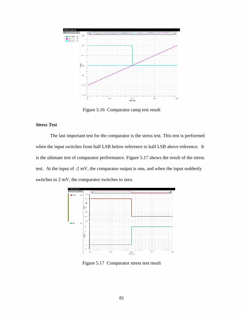
81
Figure 5.16 Comparator ramp test result
Stress Test
The last important test for the comparator is the stress test. This test is performed
when the input switches from half LSB below reference to half LSB above reference. It
is the ultimate test of comparator performance. Figure 5.17 shows the result of the stress
test. At the input of -2 mV, the comparator output is one, and when the input suddenly
switches to 2 mV, the comparator switches to zero.
Figure 5.17 Comparator stress test result
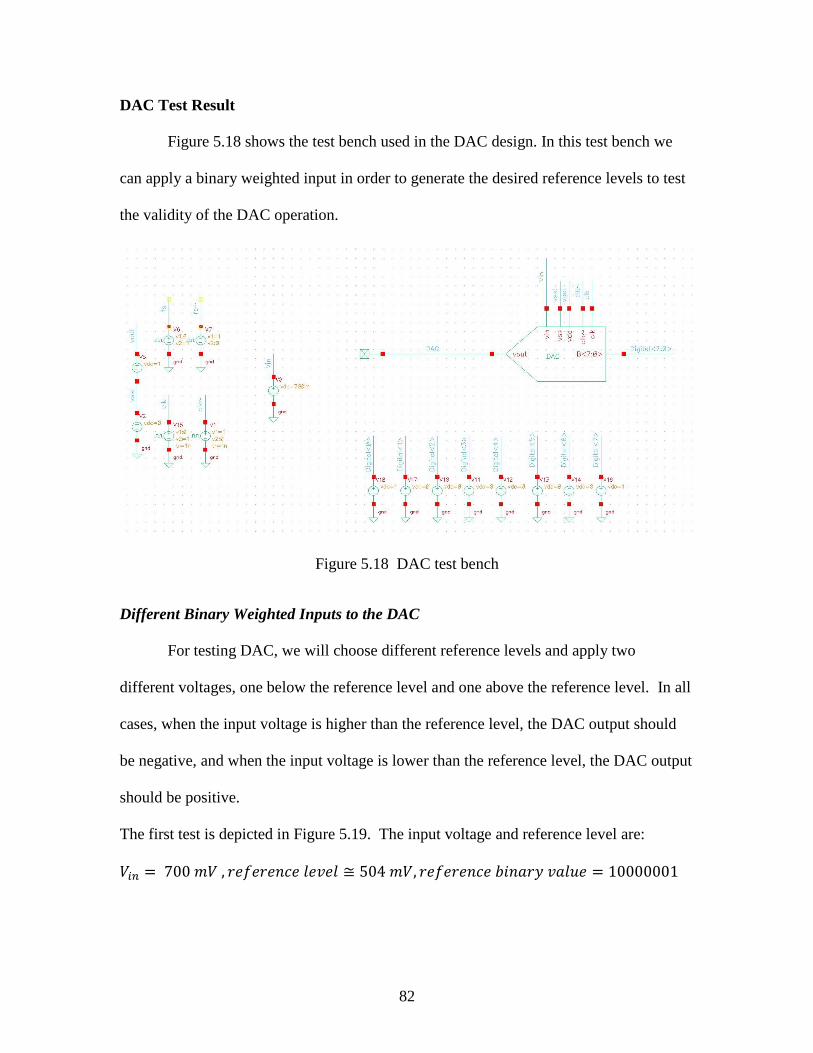
82
DAC Test Result
Figure 5.18 shows the test bench used in the DAC design. In this test bench we
can apply a binary weighted input in order to generate the desired reference levels to test
the validity of the DAC operation.
Figure 5.18 DAC test bench
Different Binary Weighted Inputs to the DAC
For testing DAC, we will choose different reference levels and apply two
different voltages, one below the reference level and one above the reference level. In all
cases, when the input voltage is higher than the reference level, the DAC output should
be negative, and when the input voltage is lower than the reference level, the DAC output
should be positive.
The first test is depicted in Figure 5.19. The input voltage and reference level are:

83
Figure 5.19 DAC test result
Figure 5.20 shows the next test results for
Figure 5.20 DAC test result

84
Next, we applied a different reference voltage and a different set of input voltages
and came up with the following results that are shown in 5.21.
Figure 5.21 DAC test result
Figure 5.22 shows the next test results for

85
Figure 5.22 DAC test result
Again, we applied a different reference voltage and different set of input voltages
and produced the following results. Shown in Figure 5.23.
Figure 5.23 DAC test result

86
Figure 5.24 shows the next test results for
Figure 5.24 DAC test result
The procedure was repeated using a different reference voltage and different set
of input voltages and came up with the following results. Shown in Figure 5.25.
Figure 5.25 DAC test result
Figure 5.26 shows the next test results for

87
Figure 5.26 DAC test result
Applying yet another reference voltage and set of input voltages yielded the
following results, Shown in Figure 5.27.
Figure 5.27 DAC test result
Figure 5.28 shows the next test results for

88
Figure 5.28 DAC test result
As can be seen in the figure, no matter what the input voltage was or how far
below or above the reference level it was, the DAC was able to generate the voltage
difference. This is a result of the meticulous design of the capacitors and switches.
DAC Stress Test
The final test for the DAC block is the stress test, when the input to the DAC is
half LSB below the reference level and suddenly switches to half LSB above the
reference level. Figure 5.29 shows the stress test result for DAC.

89
Figure 5.29 DAC stress test result
The stress test demonstrates that the DAC is capable of generating the correct
values.
SAR ADC Tests
Figure 5.30 illustrates the test bench we used to test the SAR ADC as a whole
system. We were able to give appropriate inputs and observe different nodes of the
system, such as comparator decision, DAC output, and the logic decision that is the final
digital output.

90
Figure 5.30 Proposed SAR test bench
Test Result for DC Analog Input
Figure 5.31 shows the result for a single input of 38 mV to the SAR ADC system.
Figure 5.31 Test result for proposed SAR
As is apparent from the figure, the comparator has made decisions based on the
DAC inputs. The logic starts the operation with the sampling clock. The final value for
the logic is 00001001, equal to 35 mV, which is the closest reference level to the input
voltage. The power consumption for this test was 2.1 uW.

91
Future work will include a ramp test, generating INL and DNL, and a tone test.
The results should enable us to calculate SQNR, SNDR, and other useful parameters.
Conclusion
In conclusion, in this project a novel comparator architecture for low-power
ADCs was presented. Based on the proposed comparator, a low-power SAR ADC for
bio-medical implant devices was designed. The power consumption of 2.1 µW is
instrumental in low-power electronic applications. The test results for different blocks,
sub-system, and circuitry of this system demonstrated a high level of performance. The
overall performance of designed ADC proved to be acceptable for the proposed
applications.
References
[1] J. L. McCreary and P. R. Gray, "All-MOS Charge Redistribution Analog to-Digital
Conversion Techniques-Part I," IEEEJ. Solid-State Circuits, vol. SC-IO, pp. 371-
379, Dec. 1975.
[2] B. Fotouhi and D. A. Hodges, "High-Resolution AID Conversion in MOSILSI,"
IEEE J. Solid-State Circuits, vol. SC-14, pp. 920-926, Dec. 1979.
[3] K. Bacrania, "A 12-Bit Successive-Approximation-Type ADC with Digital Error
Correction," IEEEJ. Solid-State Circuits, vol. SC-21, pp. 10161025, Dec. 1986.
[4] R. K. Hester et al., "Fully Differential ADC with Rail-to-Rail Common Mode
Range and Nonlinear Capacitor Compensation," IEEE J. Solid State Circuits, vol.
SC-25, pp. 173-183, Feb. 1990.
[5] G. A. Miller, "An 18 b 10 JLS Self-Calibrating ADC," ISSCC Dig. Tech. Pap., pp.
168-169, Feb. 1990.
[6] W. Black and D. A. Hodges, "Time Interleaved Converter Arrays, "IEEE J. Solid-
State Circuits, vol. SC-15, pp. 1022-1029, Dec. 1980.

92
[7] A. Montijo and K. Rush, "Accuracy in Interleaved ADC Systems," Hewlett-
Packard J., pp. 38-46, Oct. 1993.
[8] Y. C. Jenq, "Digital Spectra of No uniformly Sampled Signals: Fundamentals and
High-Speed Waveform Digitizers," IEEE Trans. Instrum. Meas., vol. 37, pp. 245-
251, June 1988.
[9] M. T. McTigue and P. J. Byrne, "An 8-Gigasample/sec 8-Bit Data Acquisition
System for a Sampling Digital Oscilloscope," Hewlett-Packard J., pp. 11-23, Oct.
1993.
[10] C. S. G. Conroy, D. W. Cline, and P. R. Gray, "An 8-b 85-MS/s Parallel Pipelined
AID Converter in I-J.Lrn CMOS," IEEE J. Solid-State Circuits, vol. SC-28, pp.
447-454, April 1993.
[11] T. L. Brooks, D. H. Robertson, D. F. Kelly, A. Del Muro, and S. W. Harston, “A
cascaded sigma–delta pipeline A/D converter with 1.25 MHz signal bandwidth and
89 dB SNR,” IEEE International Journal of Solid State Circuits, vol. 32, no. 12,
pp. 1896–1906,1997.
[12] C. P. Hurrell, C. Lyden, D. Laing, D. Hummerston, and M. Vickery, “An 18 b
12.5 MS/s ADC with 93 dB SNR,” IEEE International Journal of Solid State
Circuits, vol. 45, no. 12, pp. 2647–2654, 2010.
[13] G. Van der Plas and B. Verbruggen, “A 150 MS/s 133 μW 7 bit ADC in 90 nm
digital CMOS,” IEEE International Journal of Solid State Circuits, vol. 43, no. 12,
pp. 2631–2640, 2008.
[14] R. Schreier and G. C. Temes, Understanding Delta–Sigma Data Converters. John
Wiley & Sons, New York, NY, 2005.
[15] C. Toumazou, J. B. Hughes, and N. C. Battersby, “Switched-Currents: an
Analogue Technique for Digital Technology”, Peter Peregrinus, Stevenage, UK,
1993, ISBN 0-86341-294-7
[16] N. Tan, “A 1.5-V 3-mW 10-bit 50 MS/s CMOS DAC with Low Distortion and
Low Intermodulation in Standard Digital CMOS Process,” in Proc. of the 1997
IEEE Custom Integrated Circuits Conf. (CICC’97), pp. 599 - 602, Santa Clara,
CA, USA, May 1997
[17] M. Ismail and T. Fiez, Analog VLSI: Signal and Information Processing,
McGraw-Hill, New York, NY, USA, 1994, ISBN 0-07-113387-9
[18] P. J. Fish, Electronic Noise and Low Noise Design, Macmillan, Basingstoke, UK,
1993, ISBN 0- 333-57310-2

93
[19] H. Inose, Y. Yasuda and J. Marakami, “A telemetering system by code
modulation, delta-sigma modulation,” IRE Trans. on Space, Electronics and
Telemetry, SET-8, pp. 204-209, Sept. 1962.
[20] W. L. Lee and C. G. Sodini, “A topology for higher order interpolative coders,”
Proc. International Symposium on Circuits and Systems, pp. 459-462, May 1987.


