Department of electronics GOVERNMENT SCIENCE COLLEGE
(Autonomous) HASSAN – 573 201
Academic year 2019 – 2020
Syllabus of B.Sc. Electronics

CONTENTS
Sl. No. Particulars
1. Subjects & Paper Code
2. Scheme of Examination
3. Scheme of IA Marks Distribution
4. Question Paper Pattern – Marks Distribution
5. Scheme of Practical Examination Marks Distribution
SYLLABUS
6. I Semester
7. II Semester
8. MODEL QUESTION PAPER
S emes t er , Pa p er co d e a n d T i t l e o f T h eo ry a n d Pra c t i ca l
Semester
Code
Title of the Subject –
Theory
Code
Title of the Subject -
Practical
I ELT
1.0
Basic Electronics and
Network Theorems
ELP
1.0
Basic Electronics and
Network Theorems Lab
II ELT
2.0
Analog Electronic Circuit
Design
ELP
2.0
Amplifiers and Oscillators
Lab

Scheme of Examination
Sem Paper Code Title of
the Paper
Duration
in Hours
Marks
Credits IA
Marks
Exam
Marks
Total Th Pr Exam Th Pr Th Pr
I I EL
1.0
Basic
Electronics
and
Network
Theorems
3 3 3 30 15 70 35 150 4+1=5
II II EL
2.0
Analog
Electronic
Circuit
Design
3 3 3 30 15 70 35 150 4+1=5
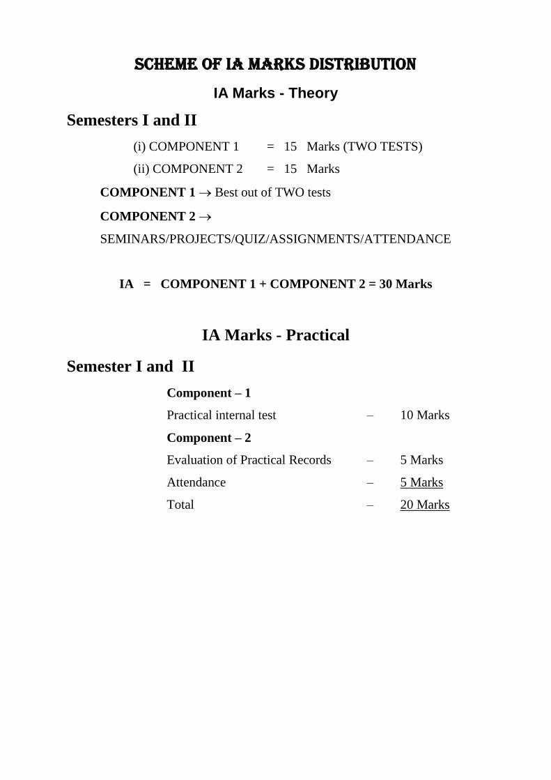
Scheme of IA marks Distribution
IA Marks - Theory
Semesters I and II
(i) COMPONENT 1 = 15 Marks (TWO TESTS)
(ii) COMPONENT 2 = 15 Marks
COMPONENT 1 Best out of TWO tests
COMPONENT 2
SEMINARS/PROJECTS/QUIZ/ASSIGNMENTS/ATTENDANCE
IA = COMPONENT 1 + COMPONENT 2 = 30 Marks
IA Marks - Practical
Semester I and II
Component – 1
Practical internal test – 10 Marks
Component – 2
Evaluation of Practical Records – 5 Marks
Attendance – 5 Marks
Total – 20 Marks

Question Paper Pattern – Marks Distribution
SEMESTERS I and II
There will be three Parts A, B, and C.
Part A is from Unit – 1 and Unit – 2, Part B is from Unit – 3 and Unit – 4 and Part C
is conceptual questions from Part A and Part B of the syllabus.
Part A, and B, each is 32 marks and Conceptual (1 Question from each unit) is for 06
Marks.
Total : 32 + 32 + 06 = 70 Marks
PART A and PART B
Each Part Marks Distribution
1. 2 mark questions – Total 4 To be answered 3 2 × 3 = 6 marks
2. 6 mark questions – Total 4 To be answered 3 6 × 3 = 18 marks
3. 4 mark problems – Total 3 To be answered 2 4 × 2 = 8 marks
4. 2 mark questions (Conceptual) – Total 4, To be answered 3, 2 × 3 = 6 marks
Each Part: Total = 32 x 2 = 64 Marks + 6 Marks (Conceptual) = 70 Marks
A conceptual question to be asked from Part A (Unit – 1 : 2 questions, Unit – 2 : 2
questions) and from Part B (Unit – 3 : 2 questions, Unit – 4 : 2 questions). Answer any
three out of 4 questions.
[Grand Total (A + B + C (Conceptual)) 70 marks]
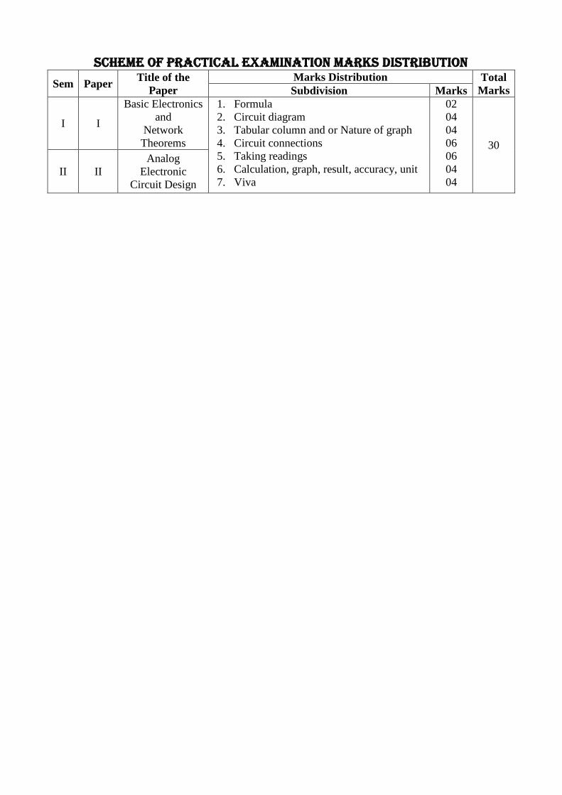
Scheme of Practical Examination marks Distribution
Sem Paper Title of the
Paper
Marks Distribution Total
Marks Subdivision Marks
I I
Basic Electronics
and
Network
Theorems
1. Formula
2. Circuit diagram
3. Tabular column and or Nature of graph
4. Circuit connections
5. Taking readings
6. Calculation, graph, result, accuracy, unit
7. Viva
02
04
04
06
06
04
04
30
II II
Analog
Electronic
Circuit Design
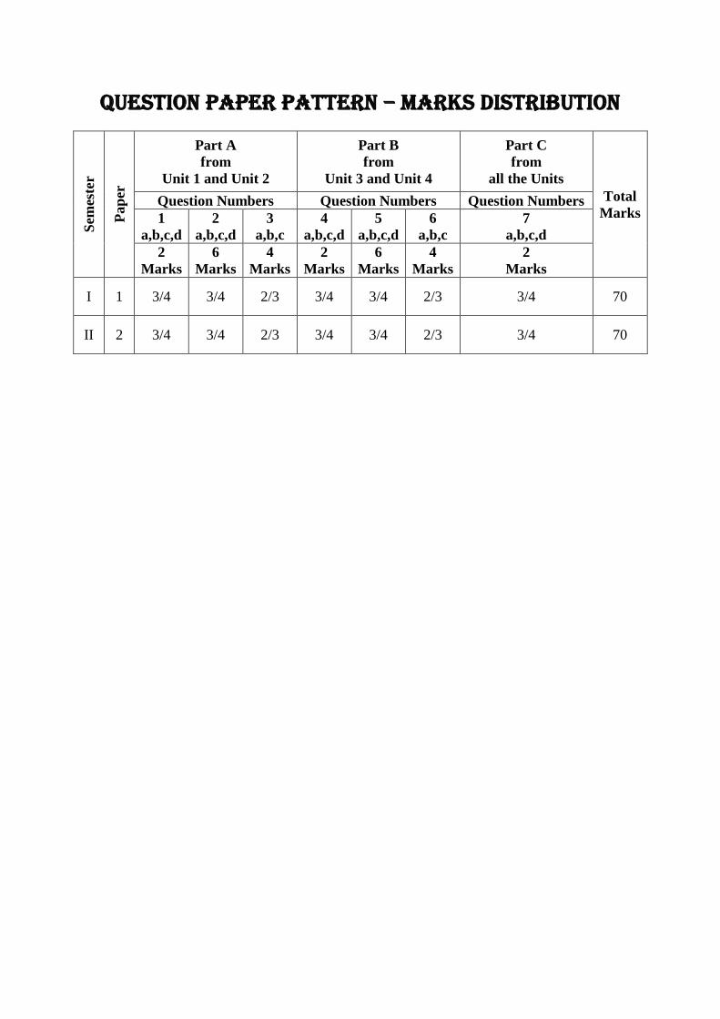
Question Paper Pattern – Marks Distribution S
emes
ter
Pap
er
Part A
from
Unit 1 and Unit 2
Part B
from
Unit 3 and Unit 4
Part C
from
all the Units
Total
Marks Question Numbers Question Numbers Question Numbers
1
a,b,c,d
2
a,b,c,d
3
a,b,c
4
a,b,c,d
5
a,b,c,d
6
a,b,c
7
a,b,c,d
2
Marks
6
Marks
4
Marks
2
Marks
6
Marks
4
Marks
2
Marks
I 1 3/4 3/4 2/3 3/4 3/4 2/3 3/4 70
II 2 3/4 3/4 2/3 3/4 3/4 2/3 3/4 70
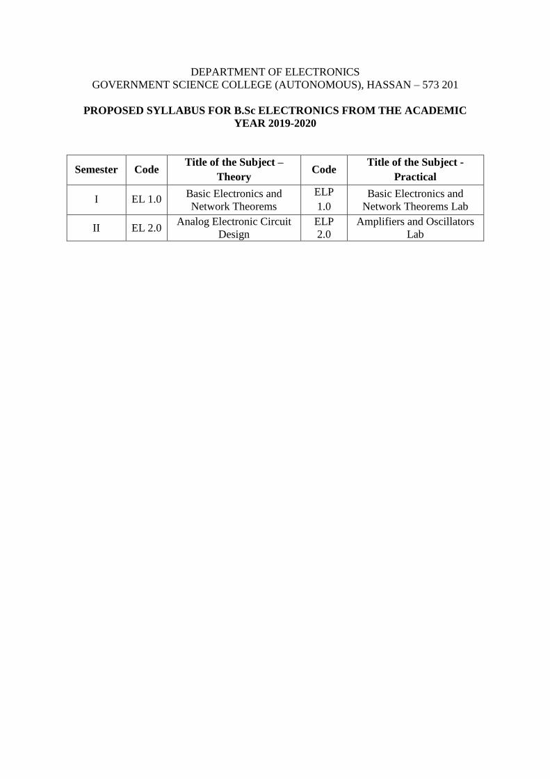
DEPARTMENT OF ELECTRONICS
GOVERNMENT SCIENCE COLLEGE (AUTONOMOUS), HASSAN – 573 201
PROPOSED SYLLABUS FOR B.Sc ELECTRONICS FROM THE ACADEMIC
YEAR 2019-2020
Semester Code Title of the Subject –
Theory Code
Title of the Subject -
Practical
I EL 1.0 Basic Electronics and
Network Theorems
ELP
1.0
Basic Electronics and
Network Theorems Lab
II EL 2.0 Analog Electronic Circuit
Design
ELP
2.0
Amplifiers and Oscillators
Lab

B.Sc. I SEMESTER
Basic Electronics and Network Theorems
CODE: ELT 1.0
Hours/week: 4 Hrs. Total teaching hours: 64 Hrs.
Examination Marks: 70
UNIT 1
Electronic components and Network theorems
Review of electronic components: Passive and active components – Definition and examples.
Classification and specifications of passive components: Resistor, Capacitor, Inductor and
transformer.
Switches: SPST, SPDT, DPST and DPDT, fuse and electromagnetic relay, MCB, ELCB, and
RCCB (Brief note on each).
Network theorems (DC analysis only): Ohms law, Kirchhoff’s laws, voltage divider and current
divider theorems, open and short circuits, branch current, mesh analysis and node voltage
method, T to π inter-conversion (derivation), Thevenin’s theorem, Norton’s theorem and inter-
conversion, Superposition theorem – statements and steps involved, Reciprocity theorem-
statement, Maximum power transfer theorem-derivation, numerical problems.
(16 Hrs.)
UNIT 2
DC and AC analysis
Transient analysis of RC and RL circuits: Series RC circuit excited by DC source – charging
& discharging of a capacitor through resistor – circuit diagram, charge/voltage at any instant
during charging and discharging – equations (with derivations), graphical representation, time
constant, numerical problems. Series RL circuit excited by DC source – circuit diagram, current
at any instant during growth and decay – equations (with derivations), graphical representation,
time constant, numerical problems.
AC applied to Series RC, RL and RLC circuits: Impedance and phase of series RC & RL circuits
(with derivations), Numerical problems. AC applied to Series and parallel RLC circuit
(relationship of impedance, voltage, current and phase), series and parallel resonance, condition
for resonance, resonant frequency, bandwidth, significance of quality factor, numerical
problems. (16 Hrs.)
UNIT 3
Electronic active components and applications:
Construction, working and characteristics of diodes: PN junction diode – DC load line, Zener
diode and LED. Rectifiers: Half wave rectifier, Full wave rectifier - centre tapped and bridge. Circuit diagrams,
working and waveforms - ripple factor & efficiency (with derivations), comparison and numerical
problems.
Filters: Types - Capacitor filter (with derivation for ripple factor), series inductor filter, LC filter,
CLC filter, circuit diagram and explanation. Ripple factor equations (mention only)
Zener diode regulator: Circuit diagram and explanation for load and line regulation, disadvantages
of Zener diode regulator, numerical problems. Transistor series regulator circuit diagram and
working.
Pulse Circuits: Clippers and clampers: Construction and working – positive, negative and
biased. (16 Hrs)

UNIT 4
Transistors and Special purpose devices Bipolar Junction Transistor: Construction, principle & working of NPN transistor, terminology.
Configuration – CE, CB, CC (mention only). Definition of α, β and γ and their interrelations,
leakage currents (mention only), Characteristics of a transistor in CE mode, numerical problems.
Transistor as a switch: Circuit and working. Junction Field Effect Transistor: P and N channel FET, Construction and working of N channel
FET, characteristics, FET parameters and their relationships, comparison of FET with BJT,
numerical problems.
MOSFET: Types, construction, working and characteristics of depletion type and enhancement
type MOSFET.
Special purpose devices: Uni-junction Transistor - Construction, working and characteristics,
equivalent circuit, intrinsic standoff ratio, relaxation oscillator - derivation of frequency of
oscillation, numerical problems. SCR - Working, V-I characteristics. Diac and Triac -
Construction, working, characteristics and applications, Tunnel diode, Varactor diode, Schottky
diode. (16 Hrs)
Text books:
1. A Text book of Electronics, R.S.Sedha, S Chand and Co., Multicolour, 3rd edition, 2012.
2. Electronic Principles , Albert Malvino & David J Bates, TMH, 7th edition-2010.
3. Introductory circuit analysis, Robert Boylstead, PHI 5th edition-2010.
Reference books:
1. Electronic Devices and circuit theory, Robert Boylstead and Louis Nashelsky, 9th Edition,
2013, PHI
2. Basic Electronics- B.L. Theraja - S. Chand and Co. 3rd edition -2012.
3. Basic Electronics and Linear circuits, N.N. Bhargava, D.C. Kulshresta and D.C Gupta -
TMH.
4. Electronic devices, David A Bell, Reston Publishing Company/DB Tarapurwala Publ.
5. Electronic devices, applications and Integrated circuits, Mathur, Kulshreshta and Chadha,
Umesh Publications.
Practical-I
ELP 1.0: BASIC ELECTRONICS LAB (Minimum of 8 experiments of the following is to be performed)
1. Verification of Thevenin’s theorem.
2. Verification of Super position theorem.
3. Verification of Maximum power transfer theorem.
4. Series resonance.
5. V-I Characteristics of a pn junction diode and draw the dc load line.
6. V-I Characteristics of a Zener diode.
7. Half wave Rectifier – without and with shunt capacitance filter.
8. Centre tapped full wave rectifier – without and with shunt capacitance filter.
9. Zener diode as voltage regulator – load and line regulation.
10. Transistor characteristics in CE mode – determination of ri, ro and β.
11. FET characteristics.
12. UJT characteristics.
13. SCR characteristics

B.Sc. II SEMESTER
Analog Electronic Circuit Design
CODE: ELT 2.0
Hours/week: 4 Hrs. Total teaching hours: 64 Hrs.
Examination Marks: 70
UNIT – 1
Transistor Biasing and H parameter Transistor biasing – need for biasing, DC load line, operating point, thermal runaway, stability and
stability factor (with derivation), numerical problems.
Different types of biasing – Fixed bias (base bias) – without and with emitter resistor, collector to
base bias, voltage divider bias and emitter bias – circuit diagrams and their working, Q point
expressions, numerical problems.
Transistor h parameter: Definition, hybrid equivalent circuit of a transistor, hybrid equivalent
circuit of a CE, CB and CC configurations. Derivation for input impedance, output impedance,
current gain, voltage gain and power gain of CE configuration in terms of h parameters,
numerical problems. (16 Hrs)
UNIT 2
Small Signal Amplifiers Single Stage Amplifiers: Classification of amplifiers based on different criteria, small signal
CE amplifier-circuit, working, frequency response, Gain in decibel, Bandwidth, Hybrid model
for CE amplifier - derivation for Av, Zin and Zout. Numerical problems. Swamped amplifier,
CC amplifier - circuit diagrams & applications (mention only), Darlington pair and its
applications (mention only).
Multistage amplifiers: Qualitative study of cascaded stages, overall gain of multistage
amplifier, loading effect. Numerical problems. Types of coupling – RC coupled, transformer
coupled and direct coupled amplifiers (working, frequency response graph, advantages and
disadvantages for each).
JFET amplifier in CS mode: Circuit and operation, equivalent circuit and expression for
voltage gain (derivation). Numerical problems. (16 Hrs)
UNIT 3
Power and Tuned amplifiers
Difference between voltage and power amplifier, classification of power amplifiers - Class A,
Class B, Class AB, Class C, Class-D and Class-S amplifiers and their comparisons.
Class A single ended power amplifier–working (Basic Class – A Amplifier) - overall efficiency
(with derivation), Transformer coupled Class A power amplifier-working, overall efficiency
(with derivation). Circuit operation of Class B push pull power amplifier overall efficiency
(with derivation), Circuit operation of complementary symmetry class B push pull power
amplifier overall efficiency (with derivation), crossover distortion, heat sinks.
Tuned amplifiers - single tuned and double tuned amplifiers – circuit diagram, working and
frequency response for each, limitations of single tuned amplifier, brief note on use of tuned
amplifiers in communication circuits. (16 Hrs)

UNIT 4
Feedback circuits and Oscillators
Feedback circuits: Types, Effect on gain, input, output resistances and bandwidth – with
derivations.
Oscillators: Classification, basic principle of oscillations. Barkhausen criterion (Derivation).
Tuned Collector, Colpitt’s, Hartley, Phase shift, Wien bridge oscillators. Frequency and
condition for sustained oscillations, Crystal oscillators (with Derivations).
Multivibrators: Monostable, Bistable and Astable multivibrators – derivations for expressions,
Numerical Problems (16 Hrs)
Practical-II
ELP 2.0: BASIC ELECTRONICS LAB
(Minimum of 8 experiments of the following is to be performed)
1. Voltage divider bias – DC load line
2. CE Amplifier – frequency response.
3. CC amplifier – frequency response.
4. Tuned amplifier – frequency response
5. Common source FET amplifier
6. UJT relaxation oscillator.
7. Voltage feedback amplifier – effect on gain and bandwidth
8. Colpitt’s oscillator
9. Hartley oscillator
10. Phase shift oscillator
11. Wien bridge oscillator
12. Astable Multivibrator
13. Monostable Multivibrator
TEXT BOOKS:
1. A Text book of Electronics, R.S.Sedha, S Chand and Co., Multicolour, 3rd
edition , 2012.
2. Electronic Principles , Albert Malvino & David J Bates, TMH, 7th edition-2010
3. Electronic Devices And Circuit Theory – Robert L Boylestad And Louis Nashelsky (
PHI )
4. Basic Electronics-Solid State – B L Theraja - S Chand And Company Ltd
5. Electronics Fundamentals and Applications – D. Chattopadhyay and P.C. Rakshit
New Age International Publishers
REFERENCE BOOKS
1. Basic Electronics – Bernord Grob - Tata Mcgraw-Hill Publishing Company Limited,
New Delhi.
2. Basic Electronics And Linear Circuits – N N Bhargava, D C Kulshreshtha And S C
Gupta, Tata McGraw-Hill Publishing Company Limited, New Delhi.
MODEL QUESTION PAPER


