TECHNICAL UNIVERSITY OF CRETEELECTRONIC AND COMPUTER ENGINEERING DEPARTMENT
TELECOMMUNICATIONS DIVISION
Custom Over The Air Programmable
Embedded Radios
by
Eleftherios Kampianakis
A THESIS SUBMITTED IN PARTIAL FULFILLMENT OFTHE REQUIREMENTS FOR THE DIPLOMA DEGREE OF
ELECTRONIC AND COMPUTER ENGINEERING
November 2011
THESIS COMMITTEE
Assistant Professor Aggelos Bletsas, Thesis SupervisorProfessor Konstantinos Kalaitzakis
Assistant Professor Ioannis Papaefstathiou

Abstract
This thesis develops hardware, middleware and software towards a custom
and low-cost remotely programmable radio network testbed. Such testbed is
envisioned as a tool for the telecom researcher to develop, deploy and debug
radio network projects and applications. To the best of the author’s knowl-
edge, this is the first attempt towards a radio network testbed, designed
and built in a Greek university from first principles. Key features of the
testbed include: simplicity of use, reliability and remote programmability.
Furthermore, each carefully designed wireless transceiver node enables envi-
ronmental sensing and personal computer interfacing at a relatively low cost
(e30 bill of materials for each transceiver assuming relatively small quanti-
ties), due to in-house design and fabrication. The proposed testbed consists
of various software and hardware components designed to facilitate experi-
mental work for the telecom engineer/researcher. Functional demonstrations
are presented, including remotely programmable relay networks as well as
medium access control networks.
Thesis Supervisor: Assistant Prof. Aggelos Bletsas
Telecom Lab, ECE Department, TUC.
3
Table Of Contents
Table of Contents . . . . . . . . . . . . . . . . . . . . . . . . . . . . 3
List of Figures . . . . . . . . . . . . . . . . . . . . . . . . . . . . . . 6
List Of Abbreviations . . . . . . . . . . . . . . . . . . . . . . . . . 8
1 Introduction . . . . . . . . . . . . . . . . . . . . . . . . . . . . . 9
1.1 Wireless Sensor Networks, a brief review . . . . . . . . . . . . 9
1.2 Prior art in the field . . . . . . . . . . . . . . . . . . . . . . . 10
2 Hardware . . . . . . . . . . . . . . . . . . . . . . . . . . . . . . . 12
2.1 Node specifications . . . . . . . . . . . . . . . . . . . . . . . . 12
2.1.1 MCU . . . . . . . . . . . . . . . . . . . . . . . . . . . 12
2.1.2 Radio module . . . . . . . . . . . . . . . . . . . . . . 12
2.1.3 Printed Circuit Board Design . . . . . . . . . . . . . . 14
2.2 Extension Board (XTboard) . . . . . . . . . . . . . . . . . . . 15
2.2.1 Description . . . . . . . . . . . . . . . . . . . . . . . . 15
2.2.2 Design Constraints . . . . . . . . . . . . . . . . . . . . 17
2.2.3 How to use the XTboard . . . . . . . . . . . . . . . . 19
3 Point to Point Communication and CSMA/CA Middleware 21
3.1 Reliable Data Transfer . . . . . . . . . . . . . . . . . . . . . 21
3.1.1 Protocol Description . . . . . . . . . . . . . . . . . . . 21
3.1.2 How to use Reliable Data Transfer . . . . . . . . . . . 26
3.2 Carrier Sense Multiple Access with Collision Avoidance (CS-
MA/CA) . . . . . . . . . . . . . . . . . . . . . . . . . . . . . 27
3.2.1 Protocol Description . . . . . . . . . . . . . . . . . . . 27
Table Of Contents 4
3.2.2 How to use CSMA/CA . . . . . . . . . . . . . . . . . 31
4 Over The Air Programmability Middleware . . . . . . . . . 33
4.1 Important OTAP Definitions . . . . . . . . . . . . . . . . . . 35
4.1.1 In system programmable Flash memory . . . . . . . . 35
4.1.2 Compilation and download process . . . . . . . . . . . 36
4.1.3 Intel Hex Code File . . . . . . . . . . . . . . . . . . . 37
4.1.4 STARTUP.A51 file . . . . . . . . . . . . . . . . . . . . 38
4.1.5 XXXX.M51 file . . . . . . . . . . . . . . . . . . . . . . 39
4.1.6 Interrupt vectors . . . . . . . . . . . . . . . . . . . . . 39
4.2 Middleware developed . . . . . . . . . . . . . . . . . . . . . . 40
4.2.1 Bootloader . . . . . . . . . . . . . . . . . . . . . . . . 40
4.2.2 User application . . . . . . . . . . . . . . . . . . . . . 47
4.2.3 Interrupt pseudo-vector . . . . . . . . . . . . . . . . . 48
4.2.4 Gateway Firmware Updater . . . . . . . . . . . . . . . 51
4.3 How to use Over The Air Programming . . . . . . . . . . . . 55
4.3.1 Files needed and their description . . . . . . . . . . . 56
4.3.2 Setting up the application to be bootload-able . . . . 56
4.3.3 Setting up and Installing the bootloader . . . . . . . . 58
4.3.4 Using master firmware updater to program over the air 58
4.3.5 Over The Air Programmed “Blinky” Demo (“Hello
World” example) . . . . . . . . . . . . . . . . . . . . . 60
5 Demos and applications . . . . . . . . . . . . . . . . . . . . . . 65
5.0.6 Application Description . . . . . . . . . . . . . . . . . 67
5.0.7 Network debugging tool . . . . . . . . . . . . . . . . . 69
6 Conclusion and future/ongoing work . . . . . . . . . . . . . . 71
6.1 Future/Ongoing Work . . . . . . . . . . . . . . . . . . . . . . 71
6.2 Challenges during development . . . . . . . . . . . . . . . . . 73
6.3 Conclusion . . . . . . . . . . . . . . . . . . . . . . . . . . . . 74
Table Of Contents 5
Appendices
A Gateway Code . . . . . . . . . . . . . . . . . . . . . . . . . . . . 75
B Blinky code . . . . . . . . . . . . . . . . . . . . . . . . . . . . . . 77
C Demo codes . . . . . . . . . . . . . . . . . . . . . . . . . . . . . 81
C.1 LED Blinking . . . . . . . . . . . . . . . . . . . . . . . . . . . 81
C.2 Relay system with direction from node 6 to 3 . . . . . . . . . 81
C.3 Relay system with direction from node 3 to 6 . . . . . . . . . 83
C.4 Broadcast system . . . . . . . . . . . . . . . . . . . . . . . . 84
C.5 CSMA/CA system . . . . . . . . . . . . . . . . . . . . . . . . 85
C.6 Demo code configuration library . . . . . . . . . . . . . . . . 86
Bibliography . . . . . . . . . . . . . . . . . . . . . . . . . . . . . . . 87
6
List of Figures
2.1 Printed circuit board (PCB) design and prototype of iCubes
v0.2. . . . . . . . . . . . . . . . . . . . . . . . . . . . . . . . . 14
2.2 XTboard Layout . . . . . . . . . . . . . . . . . . . . . . . . . 16
2.3 XTboard constraints figure. . . . . . . . . . . . . . . . . . . . 17
2.4 XTboard on iCubes node in vertical position. . . . . . . . . . 18
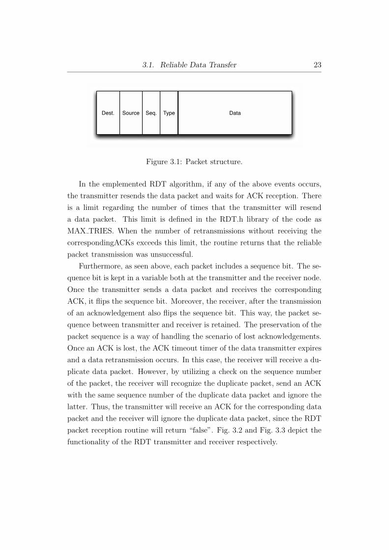
3.1 Packet structure. . . . . . . . . . . . . . . . . . . . . . . . . . 23
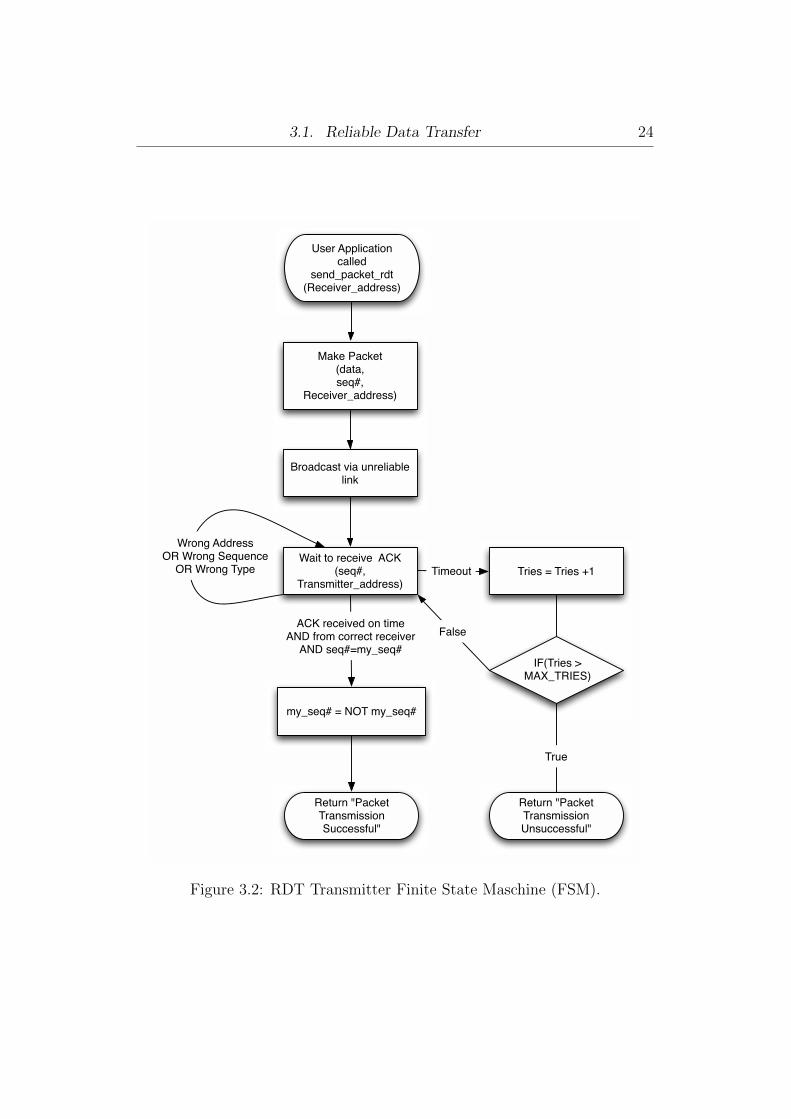
3.2 RDT Transmitter Finite State Maschine (FSM). . . . . . . . . 24
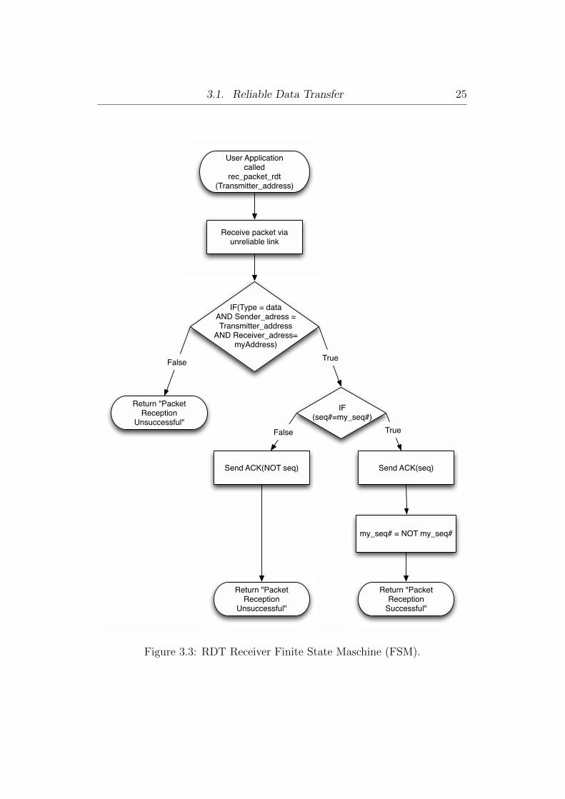
3.3 RDT Receiver Finite State Maschine (FSM). . . . . . . . . . . 25
3.4 CSMA Transmitter FSM. . . . . . . . . . . . . . . . . . . . . 29
3.5 CSMA Receiver FSM. . . . . . . . . . . . . . . . . . . . . . . 30
4.1 Programming 4 nodes with OTAP. . . . . . . . . . . . . . . . 34
4.2 Programming 4 nodes with debug adapter. . . . . . . . . . . . 34
4.3 Program execution control flow. . . . . . . . . . . . . . . . . . 45
4.4 Interrupt servicing flow. . . . . . . . . . . . . . . . . . . . . . 50
4.5 The program flow of the gateway firmware . . . . . . . . . . . 51
4.6 Gateway file reception procedure through RS232 interface. . . 53
4.7 Compression of two characters into one byte. . . . . . . . . . . 55
4.8 The contents of flash memory, after the successful installation
of the interrupt handler, the bootloader and application. . . . 59
5.1 Demo setup. . . . . . . . . . . . . . . . . . . . . . . . . . . . . 65
5.2 Relay demo presentation. . . . . . . . . . . . . . . . . . . . . . 68
5.3 Sniffer functionality with relay system. . . . . . . . . . . . . . 70


List Of Abbreviations 8
List Of Abbreviations
MCU MicroController Unit
ADC Analog to Digital Converter
WSN Wireless Sensor Network
IC Integrated Circuit
CPU Central Processing Unit
OTAP Over The Air Programming
RSSI Received Signal Strength Indication
OS Operating System
RTOS Real Time Operating System
KB Kilo Byte (1024 Bytes)
FSK Frequency Shift Keying
MSK Minimum Shift Keying
SMD Sourface Mount Device
SMT Surface Mount Type
SMA SubMiniature version A connector
PCB Printed Circuit Board
CAD Computer Aided Design
AGC Automatic Gain Control
CRC Cyclic Redundancy Check
RDT Reliable Data Transmission
LBT Listen Before Talk
CSMA/CA Carrier Sense Multiple Access with Collision Avoidance
IDE Integrated Development Environment
Hex Hexadecimal
FSM Finite State Machine
EOT End Of Transmission
EOF End Of File
LED Light Emitting Diode
ISR Interrupt Service Routine
UHF Ultra High Frequency
DIP Dual In-line Package
Chapter 1
Introduction
1.1 Wireless Sensor Networks, a brief review
Nowadays the need for telecommunications at all levels has become critical
for all modern societies. To meet such need, new discoveries in all scientific
fields have been made, leveraging telecommunications at totally new levels.
One of the greatest achievements in the telecom field are the design of wireless
sensor networks (WSNs).
A WSN is a network consisting of a number of small units that can
communicate with each other and can sense environmental variables such as
temperature, luminosity, humidity e.t.c. Each such unit is called a node and
it consists of several parts.
To start with, every node requires a processing unit. For this purpose, a
micro controller unit (MCU) is utilized. More specifically, MCUs are devices
that can perform calculations, analog to digital conversions and interface
with each node’s peripherals. The characteristics that separate MCUs from
other processing units (e.g x86 CPUs) are the low power operation, the small
form factor and the extremely low cost (starting even from 2 cents).
Furthermore every WSN node utilizes a wireless radio communication
module. This module is controlled by the MCU in order for the node to act
as a transceiver of data from and to other nodes. Similarly to the MCU, the
radio module is of low cost, small and demands low power. It can be easily
seen that multiple nodes like the one described above can form a network.
Moreover, another important part of the WSN node is its power source,
which is usually a battery and/or an energy harvesting device (for example
a solar panel). Finally WSNs being sensor networks, make use of sensors in
order to extract data from the environment.

1.2. Prior art in the field 10
1.2 Prior art in the field
Wireless sensor networks is a technology that is under development for more
than 15 years. Therefore, a large number of implementations have been
presented so far. Cited bellow is a list1 with a number of popular WSN
nodes:
1. Crossbow TelosB [17]
2. Crossbow Micaz/Mica2 [19]
3. Memsic IRIS [5]
4. Memsic LOTUS [4]
5. ETH University BTnode [18]
6. Coalesenses iSense [3]
7. Libelium Waspmote [2]
Our work in [21] provides a comparative study between the node described
in this thesis and commercial Micaz, Isense and BTnode. The comparison
regards features such as the battery life, wireless and wired connectivity
capabilities, programming environment, etc. According to the study, the
node developed (namely iCubes2) competes with other WSN nodes, either
commercial or academic. A more extensive comparison between all referenced
node implementations is beyond the scope of this thesis.
Nevertheless, it could be noted that the wireless sensor network developed
is mainly focused in telecommunication research and education. More specif-
ically, software and hardware developed were engineered in order to be easily
used by a telecommunication engineer not specialized in embedded systems.
For this reason, all firmware was written in plain C and usage of complex
real time operating systems (RTOS) such as tinyOS [13] was avoided. More-
over, an MCU with a finely written manual was selected in order to facilitate
1A more comprehensive list of available wireless sensor nodes is cited in [6]2The term “iCube” has been also used for an R&D Group [?] and a visualization
studio [?]

1.2. Prior art in the field 11
micro-controller familiarization, which at most cases is a crucial factor of de-
velopment delay. Finally, the remote programmability that was developed,
does not require the use of a RTOS. This is a powerful feature of this work.
On the other hand, the nodes listed above focus mainly in sensing appli-
cations developed by embedded system engineers. For this reason, supported
functions such as remote programmability, are unavailable without the use
of a RTOS. This property is not desired by an engineer who is not familiar
with firmware development using the principals of embedded operating sys-
tems and embedded systems in general. Moreover, operating systems such
as tinyOS require complex installation procedures which add an extra delay
to the total development time of a project. Finally, the manuals of MSP430
and ATmega MCUs, utilized by most of the popular WSN nodes are not that
easily readable compared to the manual of the C8051F320 MCU, utilized in
the iCubes node (this work).
Chapter 2
Hardware
2.1 Node specifications
The node was developed as a project of the Analysis and Design(Synthesis)
of Telecom Modules course during the 2009 spring semester [20]. Below is a
brief description of the node specifications.
2.1.1 MCU
The microcontroller unit is the C8051F320 [11] from Silicon Laboratories [1].
It incorporates an 8051 core, a 10-bit Analog to Digital Converter (ADC),
two comparators, 2304 KB of RAM and 16KB of flash memory. The main
reason this MCU was selected is the finely written manual. This facilitates
the development of research programs as well as complex applications. More-
over, the 8051 instruction set is widely known, therefore making application
development easier. Finally C8051F320 is designed for low power operation
without compromising variety of peripherals, flexibility and battery life.
2.1.2 Radio module
The radio module is the Chipcon/TI CC2500 [12] transceiver. Its frequency
of operation is at the 2.4 GHz band with maximum transmit power of 1 dBm
and programmable rate up to 0.5 Mbps. It was selected due to its wide range
of tunable parameters regarding digital communication that can be easily set
by modifying specific control registers.

2.1. Node specifications 13
Listed below are some of the radio parameters that can be adjusted:
• carrier frequency and frequency channel (parameterized for frequency
hopping applications),
• transmission power,
• type of FSK modulation and respective frequency deviation (continuous
phase FSK i.e. MSK, is also supported),
• OOK modulation,
• variable rate and receiver filter bandwidth,
• number of preamble bits used for bit-level synchronization,
• number of bytes used for byte-level synchronization (sync word),
• receive signal strength indication (RSSI) activation and automatic gain
control (AGC),
• cyclic redundancy check (CRC).
2.1. Node specifications 14
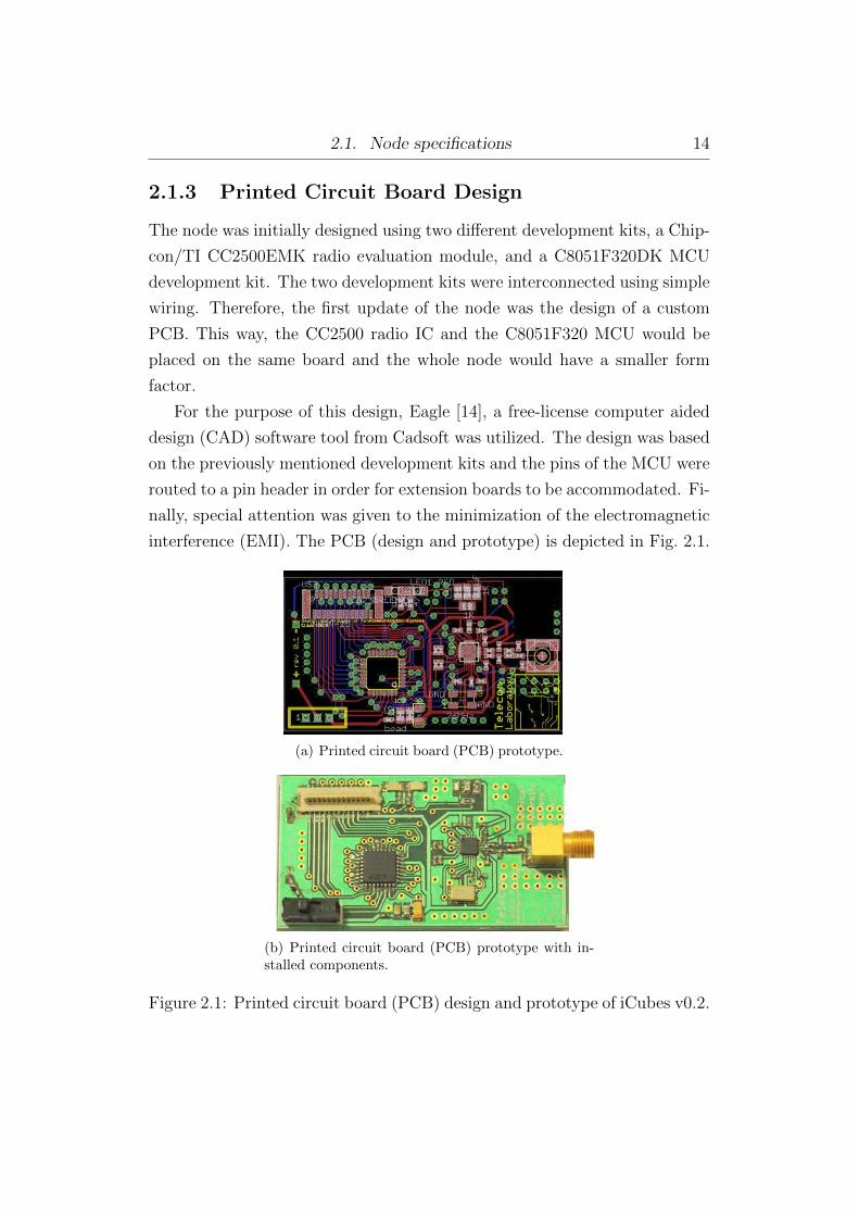
2.1.3 Printed Circuit Board Design
The node was initially designed using two different development kits, a Chip-
con/TI CC2500EMK radio evaluation module, and a C8051F320DK MCU
development kit. The two development kits were interconnected using simple
wiring. Therefore, the first update of the node was the design of a custom
PCB. This way, the CC2500 radio IC and the C8051F320 MCU would be
placed on the same board and the whole node would have a smaller form
factor.
For the purpose of this design, Eagle [14], a free-license computer aided
design (CAD) software tool from Cadsoft was utilized. The design was based
on the previously mentioned development kits and the pins of the MCU were
routed to a pin header in order for extension boards to be accommodated. Fi-
nally, special attention was given to the minimization of the electromagnetic
interference (EMI). The PCB (design and prototype) is depicted in Fig. 2.1.
(a) Printed circuit board (PCB) prototype.
(b) Printed circuit board (PCB) prototype with in-stalled components.
Figure 2.1: Printed circuit board (PCB) design and prototype of iCubes v0.2.

2.2. Extension Board (XTboard) 15
2.2 Extension Board (XTboard)
2.2.1 Description
Once full functionality of the node was verified and debugged, there was
urgent need for several extensions and connectivity capabilities. Such exten-
sions were:
• Programmability using the Silabs USB debug adapter.
• Power supply using the Silabs USB debug adapter.
• Power supply using an external power source (e.g. C8051F320DK 9V
power supply).
• PC connectivity with an RS232 port.
• MCU pinout interface using standard low-cost 2 mm DIP headers.
The board was designed to meet the above needs. The architecture of
the design was based on the C8051F320 development kit. For this reason,
the hardware components below were utilized:
• National Semiconductors LM2937-3.3 for the voltage regulation from
the Silabs USB debug adapter 5V power, as well as the 9V DK power
supply [15].
• Sipex SP3223EY, a +3.0V to +5.5V RS-232 transceiver for the RS-232
connectivity [16].
In addition, for the connectivity of the RS232 interface, the power source and
the programming interface, an RS232 D-Sub connector, a power jack (barrel
type) and 2 mm headers were also utilized in the design respectively. Finally,
for the connection between the node and the extension board, a 25 pin SMT
male connector was used. The design scheme of the XTboard is presented in
Fig. 2.2.
2.2. Extension Board (XTboard) 16
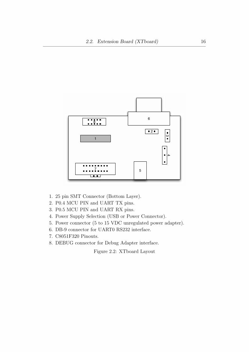
1
5
6
2
34
7
8
1. 25 pin SMT Connector (Bottom Layer).
2. P0.4 MCU PIN and UART TX pins.
3. P0.5 MCU PIN and UART RX pins.
4. Power Supply Selection (USB or Power Connector).
5. Power connector (5 to 15 VDC unregulated power adapter).
6. DB-9 connector for UART0 RS232 interface.
7. C8051F320 Pinouts.
8. DEBUG connector for Debug Adapter interface.
Figure 2.2: XTboard Layout
2.2. Extension Board (XTboard) 17
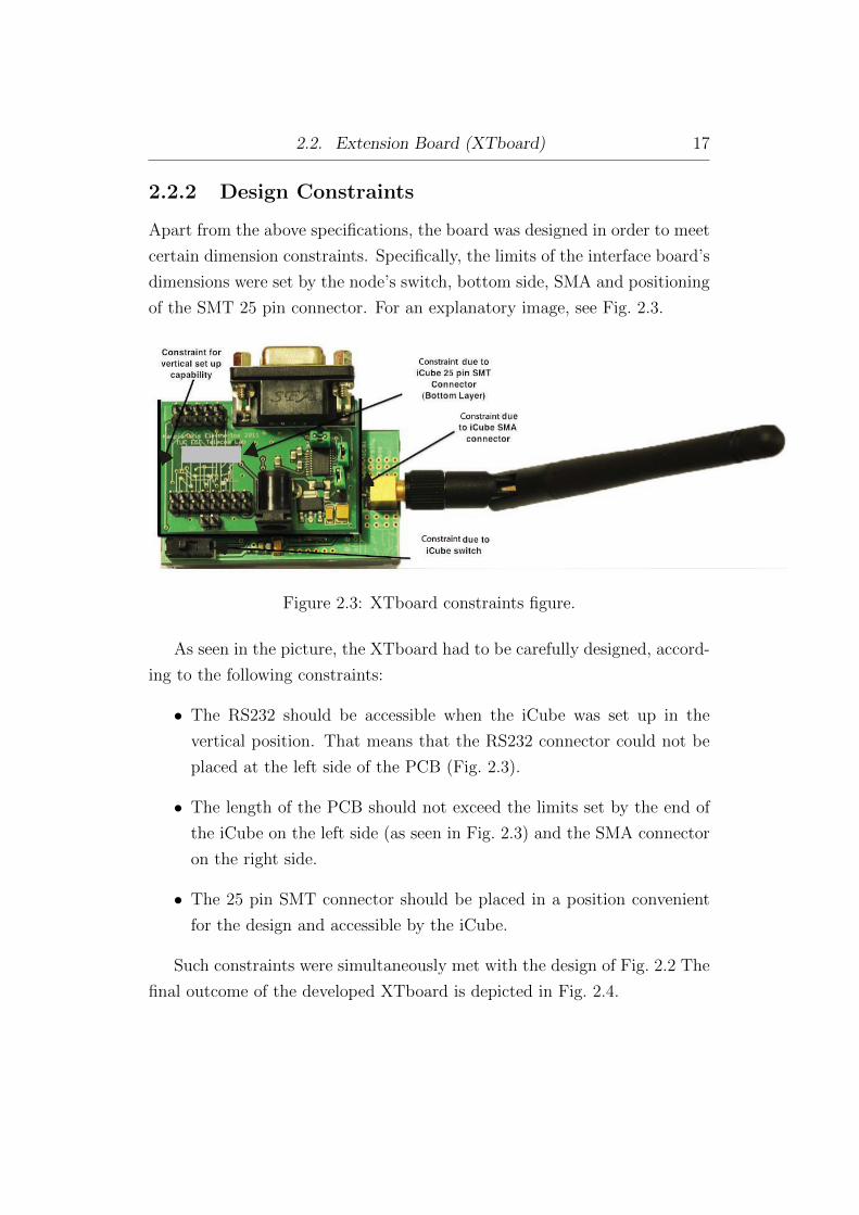
2.2.2 Design Constraints
Apart from the above specifications, the board was designed in order to meet
certain dimension constraints. Specifically, the limits of the interface board’s
dimensions were set by the node’s switch, bottom side, SMA and positioning
of the SMT 25 pin connector. For an explanatory image, see Fig. 2.3.
Figure 2.3: XTboard constraints figure.
As seen in the picture, the XTboard had to be carefully designed, accord-
ing to the following constraints:
• The RS232 should be accessible when the iCube was set up in the
vertical position. That means that the RS232 connector could not be
placed at the left side of the PCB (Fig. 2.3).
• The length of the PCB should not exceed the limits set by the end of
the iCube on the left side (as seen in Fig. 2.3) and the SMA connector
on the right side.
• The 25 pin SMT connector should be placed in a position convenient
for the design and accessible by the iCube.
Such constraints were simultaneously met with the design of Fig. 2.2 The
final outcome of the developed XTboard is depicted in Fig. 2.4.
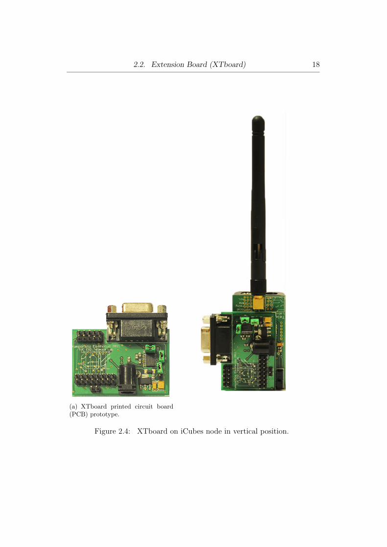
2.2. Extension Board (XTboard) 18
(a) XTboard printed circuit board(PCB) prototype.
Figure 2.4: XTboard on iCubes node in vertical position.

2.2. Extension Board (XTboard) 19
2.2.3 How to use the XTboard
Below is a set of instructions, to make use of the capabilities offered by the
extension board. For a visualization of the XTboard components see Fig. 2.2.
• RS232 connectivity:
– Use a jumper to short-circuit the P0.4 MCU pin and the RX SP322
pin.
– Use a jumper to short-circuit the P0.5 MCU pin and the TX SP322
pin.
– Connect the RS232 adapter to a PC and to the interface board.
• Power node using the 9V power supply:
– Use a jumper to short-circuit the input to the voltage regulator
and the power jack barrel connector output.
– Plug in the 9V power source into the connector.
• Power node using the Silabs USB debug adapter:
– Use a jumper to short-circuit the input to the voltage regulator
and usb power source.
– Plug in the debug adapter to the corresponding connector. A sign
is drawn on the PCB for the correct connection side.
– Connect to the device using the Silabs or Keil IDE.
• Programming interface using Silabs USB debug adapter:
– Plug in the debug adapter to the corresponding connector. There
is a sign drawn on the PCB for the correct connection side.
– Connect to the device using the Silabs or Keil IDE to download
code.

2.2. Extension Board (XTboard) 20
However, there are some particularities that the user has to look after.
Specifically:
• The power supply current should not exceed 15Volts.
• Only one power source between batteries and USB or SiLabs power
adapter must be used at a time. In the opposite case, current will flow
from the voltage regulator to the batteries.
• If The SiLabs USB Debug Adapter in not connected according to the
shape drawn on the PCB, the MCU is at risk of being burned.
• To avoid dangerous current spikes, the node must be turned of during
the connection of any peripheral.
Chapter 3
Point to Point Communication
and CSMA/CA Middleware
A critical element in the development of a WSN testbed is the communication
between nodes, in terms of reliable data transfer, medium access control and
low power transmission/reception of data. To accommodate this, a set of
primitive software functions was developed.
3.1 Reliable Data Transfer
3.1.1 Protocol Description
One of the basic principles of a successful Over The Air Programmability
(OTAP) is the establishment of a reliable connection between the master
programming gateway and the slave node. Thus, such a connection was
designed for the purposes of the OTAP and of course for general purposes.
The algorithm for a Reliable Data Transfer link (RDT), was taken from the
work done in [22]. To begin with, in order to model the real wireless channel,
the following assumptions are made :
• The channel may flip bits in the transmitted packet (either data or
acknowledgement).
• A packet can be lost during transmission.
The purpose of the RDT algorithm is to transfer a packet as reliably as
possible through an unreliable channel. To begin with, the transmitter af-
ter sending a packet shall have knowledge of the packet’s good reception.

3.1. Reliable Data Transfer 22
For this reason the receiver sends back a special packet, also known as ac-
knowledgement (ACK). The transmitter waits for the ACK for a specified
time called Timeout. Listed below are the reasons why an ACK may not be
received by the transmitter :
1. The data packet was not received from the receiver, therefore the node
did not send an ACK.
2. The data packet had flipped bits and the error detection algorithm
rejected the packet on the receiver, and the node did not send an ACK.
3. The ACK arrived to the transmitter after the timeout expired.
4. The ACK was not received at the transmitter.
5. The ACK had flipped bits and the error detection algorithm rejected
the packet on the transmitter.
Each packet includes:
• The payload data (if it is a data packet).
• The packet sequence bit.
• A field that states if the packet is data or ACK.
• The source MAC address.
• The destination MAC address.
The packet size is tunable with the use of definitions placed in the RDT.h
file, namely RXBUFFER SIZE and TXBUFFER SIZE.1.Fig. 3.1 presents
the packet structure of the RDT algorithm.
1Two separate buffers are needed for packet reception and transmission respectively.
3.1. Reliable Data Transfer 23
Dest. Source Seq. Type Data
Figure 3.1: Packet structure.
In the emplemented RDT algorithm, if any of the above events occurs,
the transmitter resends the data packet and waits for ACK reception. There
is a limit regarding the number of times that the transmitter will resend
a data packet. This limit is defined in the RDT.h library of the code as
MAX TRIES. When the number of retransmissions without receiving the
correspondingACKs exceeds this limit, the routine returns that the reliable
packet transmission was unsuccessful.
Furthermore, as seen above, each packet includes a sequence bit. The se-
quence bit is kept in a variable both at the transmitter and the receiver node.
Once the transmitter sends a data packet and receives the corresponding
ACK, it flips the sequence bit. Moreover, the receiver, after the transmission
of an acknowledgement also flips the sequence bit. This way, the packet se-
quence between transmitter and receiver is retained. The preservation of the
packet sequence is a way of handling the scenario of lost acknowledgements.
Once an ACK is lost, the ACK timeout timer of the data transmitter expires
and a data retransmission occurs. In this case, the receiver will receive a du-
plicate data packet. However, by utilizing a check on the sequence number
of the packet, the receiver will recognize the duplicate packet, send an ACK
with the same sequence number of the duplicate data packet and ignore the
latter. Thus, the transmitter will receive an ACK for the corresponding data
packet and the receiver will ignore the duplicate data packet, since the RDT
packet reception routine will return “false”. Fig. 3.2 and Fig. 3.3 depict the
functionality of the RDT transmitter and receiver respectively.
3.1. Reliable Data Transfer 24
Make Packet(data,seq#,
Receiver_address)
Wait to receive ACK(seq#,
Transmitter_address)
my_seq# = NOT my_seq#
Wrong Address OR Wrong Sequence OR Wrong Type
User Application called
send_packet_rdt(Receiver_address)
ACK received on time AND from correct receiverAND seq#=my_seq#
Broadcast via unreliable link
Return "Packet Transmission Successful"
Tries = Tries +1
IF(Tries > MAX_TRIES)
Timeout
False
Return "Packet Transmission Unsuccessful"
True
Figure 3.2: RDT Transmitter Finite State Maschine (FSM).
3.1. Reliable Data Transfer 25
User Applicationcalled
rec_packet_rdt(Transmitter_address)
Receive packet via unreliable link
IF(Type = data AND Sender_adress = Transmitter_address
AND Receiver_adress= myAddress)
Return "Packet Reception
Unsuccessful"
False
IF(seq#=my_seq#)
True
Send ACK(seq)
True
my_seq# = NOT my_seq#
Return "Packet Reception Successful"
Send ACK(NOT seq)
False
Return "Packet Reception
Unsuccessful"
Figure 3.3: RDT Receiver Finite State Maschine (FSM).
3.1. Reliable Data Transfer 26
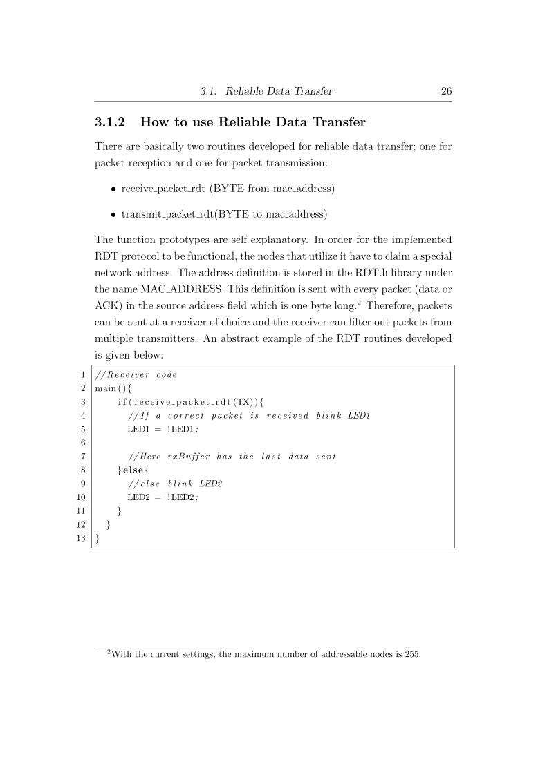
3.1.2 How to use Reliable Data Transfer
There are basically two routines developed for reliable data transfer; one for
packet reception and one for packet transmission:
• receive packet rdt (BYTE from mac address)
• transmit packet rdt(BYTE to mac address)
The function prototypes are self explanatory. In order for the implemented
RDT protocol to be functional, the nodes that utilize it have to claim a special
network address. The address definition is stored in the RDT.h library under
the name MAC ADDRESS. This definition is sent with every packet (data or
ACK) in the source address field which is one byte long.2 Therefore, packets
can be sent at a receiver of choice and the receiver can filter out packets from
multiple transmitters. An abstract example of the RDT routines developed
is given below:
1 //Receiver code
2 main ( ){3 i f ( r e c e i v e p a c k e t r d t (TX)){4 // I f a co r r e c t packe t i s r e c e i v ed b l i n k LED1
5 LED1 = !LED1 ;
6
7 //Here rxBu f f e r has the l a s t data sen t
8 } else {9 // e l s e b l i n k LED2
10 LED2 = !LED2 ;
11 }12 }13 }
2With the current settings, the maximum number of addressable nodes is 255.
3.2. Carrier Sense Multiple Access with Collision Avoidance (CSMA/CA)27
1 //Transmitter code
2 main ( ){3 i f ( s end packe t rd t (RX)){4 // I f a packe t i s t r an smi t t e r s u c c e s s f u l l y b l i n k LED1
5 LED1 = !LED1 ;
6 } else {7 // e l s e b l i n k LED2
8 LED2 = !LED2 ;
9 }10 }11 }
The above code, if downloaded to both the test transmitter and receiver
would establish a reliable link between two nodes.
3.2 Carrier Sense Multiple Access with
Collision Avoidance (CSMA/CA)
3.2.1 Protocol Description
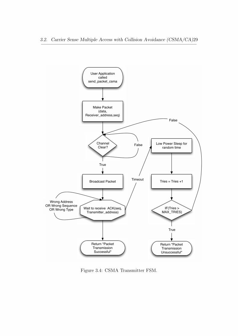
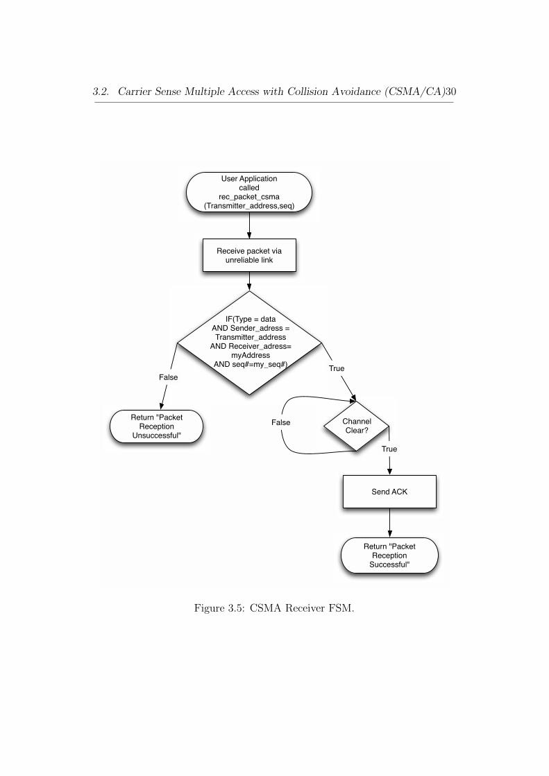
One of the fundamental communication protocols for the link layer in wire-
less networks is the Carrier Sense Multiple Access with Collision Avoidance
(CSMA/CA). The protocol described is a multiple access method that al-
lows several nodes which use the same transmission frequency channel to
transmit and share its capacity. For the developed CSMA/CA algorithm,
the following functionality is utilized:
At the transmitter side, the node listens for currently transmitted data
over the air. If data is being transmitted, the node enters sleep mode for a
random time interval. If the channel is clear, the node transmits the data,
initiates a timer to measure a timeout and waits for an ACK. If the timer
expires, the node enters sleep mode for a random time and resets the pro-
cedure. At the receiver side, the node is in receive mode and once a packet
is received, it listens to the channel for carrier power and once it is clear, it
sends back an ACK. The FSMs of the transmitter and receiver are depicted
3.2. Carrier Sense Multiple Access with Collision Avoidance (CSMA/CA)28
in Fig. 3.4 and Fig. 3.5, respectively. The type of protocols that try to trans-
mit when no packets are being transmitted simultaneously are called Listen
Before Talk (LBT).
Before the implementation of the CSMA/CA, algorithm took place, two
special functions had to be implemented: Carrier Sense function and Sleep
function. Their description follows:
Carrier Sense
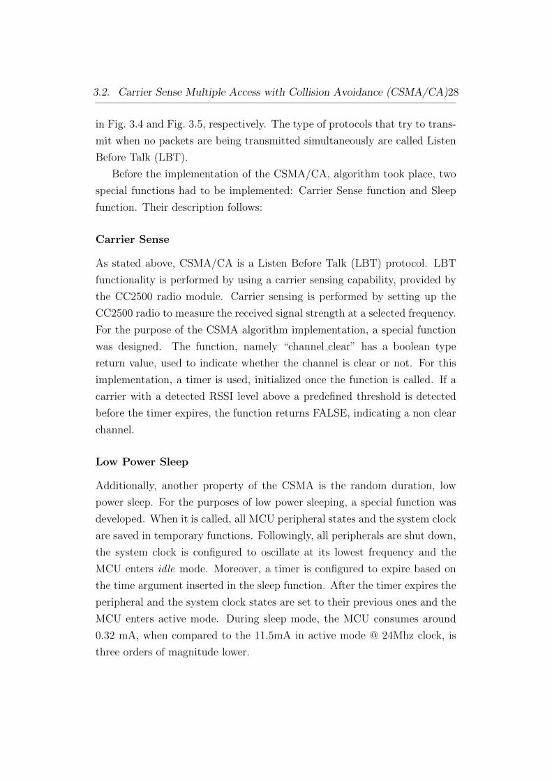
As stated above, CSMA/CA is a Listen Before Talk (LBT) protocol. LBT
functionality is performed by using a carrier sensing capability, provided by
the CC2500 radio module. Carrier sensing is performed by setting up the
CC2500 radio to measure the received signal strength at a selected frequency.
For the purpose of the CSMA algorithm implementation, a special function
was designed. The function, namely “channel clear” has a boolean type
return value, used to indicate whether the channel is clear or not. For this
implementation, a timer is used, initialized once the function is called. If a
carrier with a detected RSSI level above a predefined threshold is detected
before the timer expires, the function returns FALSE, indicating a non clear
channel.
Low Power Sleep
Additionally, another property of the CSMA is the random duration, low
power sleep. For the purposes of low power sleeping, a special function was
developed. When it is called, all MCU peripheral states and the system clock
are saved in temporary functions. Followingly, all peripherals are shut down,
the system clock is configured to oscillate at its lowest frequency and the
MCU enters idle mode. Moreover, a timer is configured to expire based on
the time argument inserted in the sleep function. After the timer expires the
peripheral and the system clock states are set to their previous ones and the
MCU enters active mode. During sleep mode, the MCU consumes around
0.32 mA, when compared to the 11.5mA in active mode @ 24Mhz clock, is
three orders of magnitude lower.
3.2. Carrier Sense Multiple Access with Collision Avoidance (CSMA/CA)29
User Application called
send_packet_csma
Make Packet(data,
Receiver_address,seq)
Broadcast Packet
Channel Clear?
False
Wait to receive ACK(seq, Transmitter_address)
Wrong Address OR Wrong Sequence OR Wrong Type
Tries = Tries +1
IF(Tries > MAX_TRIES)
Timeout
True
Return "Packet Transmission Unsuccessful"
True
Return "Packet Transmission Successful"
Low Power Sleep for random time
False
Figure 3.4: CSMA Transmitter FSM.
3.2. Carrier Sense Multiple Access with Collision Avoidance (CSMA/CA)30
User Applicationcalled
rec_packet_csma(Transmitter_address,seq)
Receive packet via unreliable link
IF(Type = data AND Sender_adress = Transmitter_address
AND Receiver_adress= myAddress
AND seq#=my_seq#)
Return "Packet Reception
Unsuccessful"
False
Send ACK
Return "Packet Reception Successful"
Channel Clear?
False
True
True
Figure 3.5: CSMA Receiver FSM.
3.2. Carrier Sense Multiple Access with Collision Avoidance (CSMA/CA)31
3.2.2 How to use CSMA/CA
As with the RDT implementation, there are two different routines that are
utilized in order for packets to be transmitted or received. These are:
• transmit packet csma ( BYTE receiver address )
• receive packet( BYTE transmitter address )
Arguments in the functions are also the sequence number, the ACK timeout
and the carrier sensing timer timeout. An example code for the usage of the
CSMA/CA algorithm developed follows :
1 //Receiver code
2 main ( ){3 i f (MAC ADDRESS == RX){4 i f ( r e c e i v e packe t c sma (ACCEPT FROM ALL)){5 // I f a co r r e c t packe t i s r e c e i v ed b l i n k LED2
6 LED2 = !LED2 ;
7 //Here rxBu f f e r has the l a s t data sen t
8 }9 }
10 }
1 // F i r s t t r an smi t t e r code
2 main ( ){3 i f (MAC ADDRESS == TX1){4 i f ( send packet csma (RX)){5 // I f a packe t i s t r an smi t t e r s u c c e s s f u l l y b l i n k LED1
6 LED2 = !LED2 ;
7 }8 }9 }
3.2. Carrier Sense Multiple Access with Collision Avoidance (CSMA/CA)32
1 //Second t r an smi t t e r code
2 main ( ){3 i f (MAC ADDRESS == TX2){4 i f ( send packet csma (RX)){5 // I f a packe t i s t r an smi t t e r s u c c e s s f u l l y b l i n k LED1
6 LED2 = !LED2 ;
7 }8 }9 }
The abstract code above depicts the functionality of the functions devel-
oped. The receiver node calls receive packet csma with an input argument
ACCEPT FROM ALL. This definition is used in the implementation of the
receive packet function, in order to disable the transmitter filter. The nodes
with addresses TX1 and TX2 enter send packet csma() using as input ar-
gument the receiver’s mac address. This way, multiple transmitters try to
access the same channel and once collision is detected, sleeping for random
time is initiated.

Chapter 4
Over The Air Programmability
Middleware
The major objective of this diploma thesis is the remote programmability of
the WSN. The normal procedure for programming one of the nodes require
physical contact with the node to be programmed.
Particularly, that means that the user needs to either move the node
from its position in the network and place it close to a computer to program
the node, or get the computer to a position close to the node where the
programming interface can be physically attached. The need for physical
contact between the programming interface and the node introduces crucial
application constrains. For example, if the node has to be set up on a location
with difficult or no human access, the node could be only programmed once,
resulting to non-updatable, error prone operation.
Moreover, the procedure for programming a wireless sensor network with
methods and devices that require physical contact is time consuming and
messy. As an example, the time required to program an iCube node using
the SiLabs debug adapter and the XTboard is about 15 to 17 seconds.1
Additionally, the movement of wiring and nodes and the repeated connection
and removal of the programming adapter can be a messy or even dangerous
procedure for node integrity. Fig. 4.2 depicts the 4 connections required in
order to program 4 iCube nodes.
The solution to this critical problem was introducing the capability wire-
less network programming, or in other words Over The Air Programmed
(OTAP). OTAP is a method of distributing firmware to a sensor network
wirelessly, thus avoiding physical contact with network nodes. With the
1Personal experiences, timings may vary.
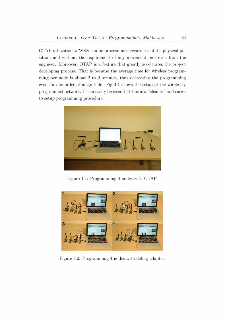
Chapter 4. Over The Air Programmability Middleware 34
OTAP utilization, a WSN can be programmed regardless of it’s physical po-
sition, and without the requirement of any movement, not even from the
engineer. Moreover, OTAP is a feature that greatly accelerates the project
developing process. That is because the average time for wireless program-
ming per node is about 2 to 3 seconds, thus decreasing the programming
even for one order of magnitude. Fig 4.1 shows the setup of the wirelessly
programmed network. It can easily be seen that this is a “cleaner” and easier
to setup programming procedure.
Figure 4.1: Programming 4 nodes with OTAP.
Figure 4.2: Programming 4 nodes with debug adapter.
4.1. Important OTAP Definitions 35
4.1 Important OTAP Definitions
Before introducing the main components required for the OTAP, some im-
portant definitions are quoted in order for the reader to be able to understand
all the aspects of this important procedure.
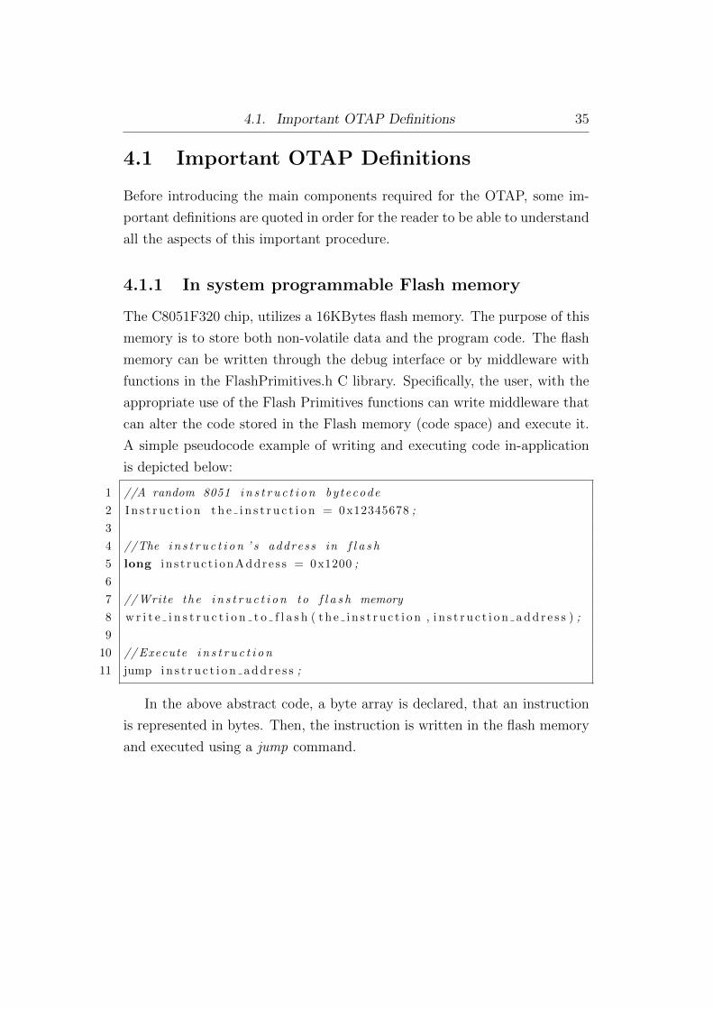
4.1.1 In system programmable Flash memory
The C8051F320 chip, utilizes a 16KBytes flash memory. The purpose of this
memory is to store both non-volatile data and the program code. The flash
memory can be written through the debug interface or by middleware with
functions in the FlashPrimitives.h C library. Specifically, the user, with the
appropriate use of the Flash Primitives functions can write middleware that
can alter the code stored in the Flash memory (code space) and execute it.
A simple pseudocode example of writing and executing code in-application
is depicted below:
1 //A random 8051 i n s t r u c t i o n by tecode
2 I n s t r u c t i o n t h e i n s t r u c t i o n = 0x12345678 ;
3
4 //The i n s t r u c t i o n ’ s address in f l a s h
5 long i n s t ruc t i onAddre s s = 0x1200 ;
6
7 //Write the i n s t r u c t i o n to f l a s h memory
8 w r i t e i n s t r u c t i o n t o f l a s h ( t h e i n s t r u c t i o n , i n s t r u c t i o n a d d r e s s ) ;
9
10 //Execute i n s t r u c t i o n
11 jump i n s t r u c t i o n a d d r e s s ;
In the above abstract code, a byte array is declared, that an instruction
is represented in bytes. Then, the instruction is written in the flash memory
and executed using a jump command.
4.1. Important OTAP Definitions 36
4.1.2 Compilation and download process
The procedure with which a C program is downloaded in the code space of
the MCU memory and specifically the C8051F320, using the Keil PK51 [?]
tool chain, is the following:
1. Preprocessing - The preprocessor handles the logic behind all the dash
(#) beginning directives of the program (Cx51 Compiler).
2. Parsing - A parse tree is created, a structure necessary for the transla-
tion step (Cx51 Compiler).
3. Translation - Assembly code object files are produced (Ax51 Assem-
bler).
4. Linking - The object files produced by the assembler are linked together
in a single object executable file (BLx51 Linker).
5. Hex File Generation - At this point a Hex file generator produces the
Hex code that will be downloaded to the device. Consult section 4.1.3
for more info.
6. Download - The final object - executable file is downloaded to the MCU
using the Silabs USB debug interface.
The step that needs to be done wirelessly in order for the OTAP to be
successful is the final one, the Download.
4.1. Important OTAP Definitions 37
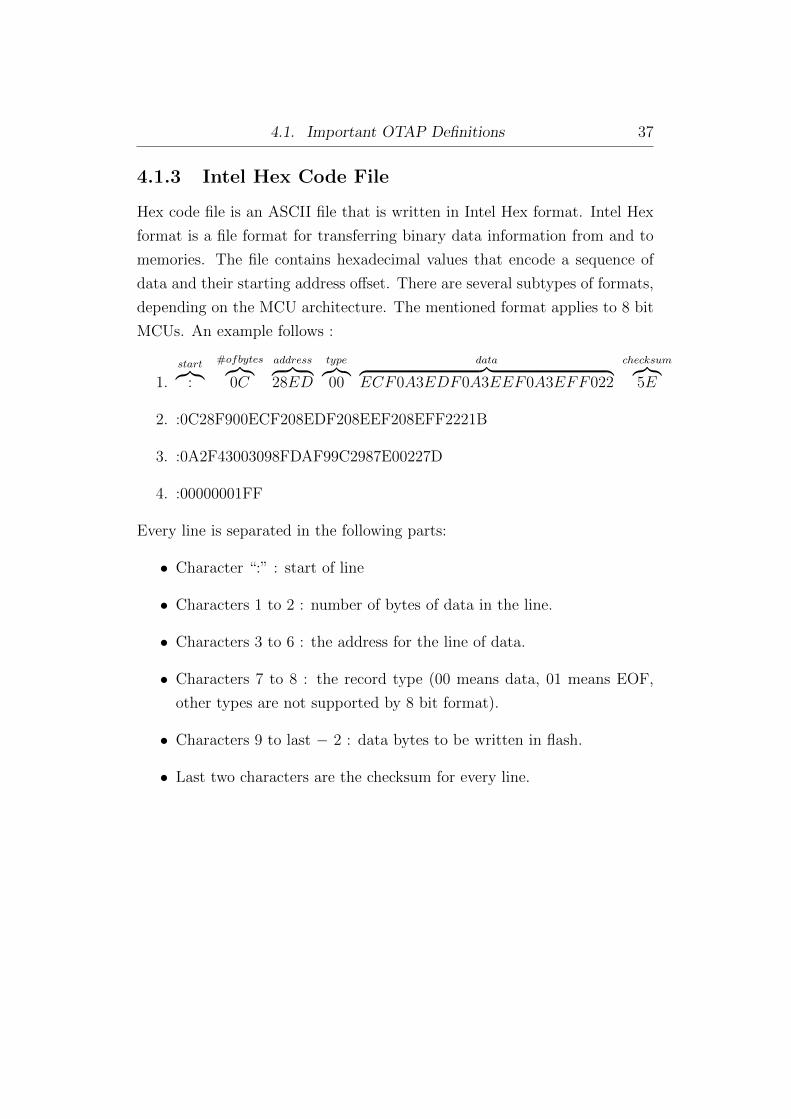
4.1.3 Intel Hex Code File
Hex code file is an ASCII file that is written in Intel Hex format. Intel Hex
format is a file format for transferring binary data information from and to
memories. The file contains hexadecimal values that encode a sequence of
data and their starting address offset. There are several subtypes of formats,
depending on the MCU architecture. The mentioned format applies to 8 bit
MCUs. An example follows :
1.start︷︸︸︷
:
#ofbytes︷︸︸︷0C
address︷ ︸︸ ︷28ED
type︷︸︸︷00
data︷ ︸︸ ︷ECF0A3EDF0A3EEF0A3EFF022
checksum︷︸︸︷5E
2. :0C28F900ECF208EDF208EEF208EFF2221B
3. :0A2F43003098FDAF99C2987E00227D
4. :00000001FF
Every line is separated in the following parts:
• Character “:” : start of line
• Characters 1 to 2 : number of bytes of data in the line.
• Characters 3 to 6 : the address for the line of data.
• Characters 7 to 8 : the record type (00 means data, 01 means EOF,
other types are not supported by 8 bit format).
• Characters 9 to last − 2 : data bytes to be written in flash.
• Last two characters are the checksum for every line.
4.1. Important OTAP Definitions 38
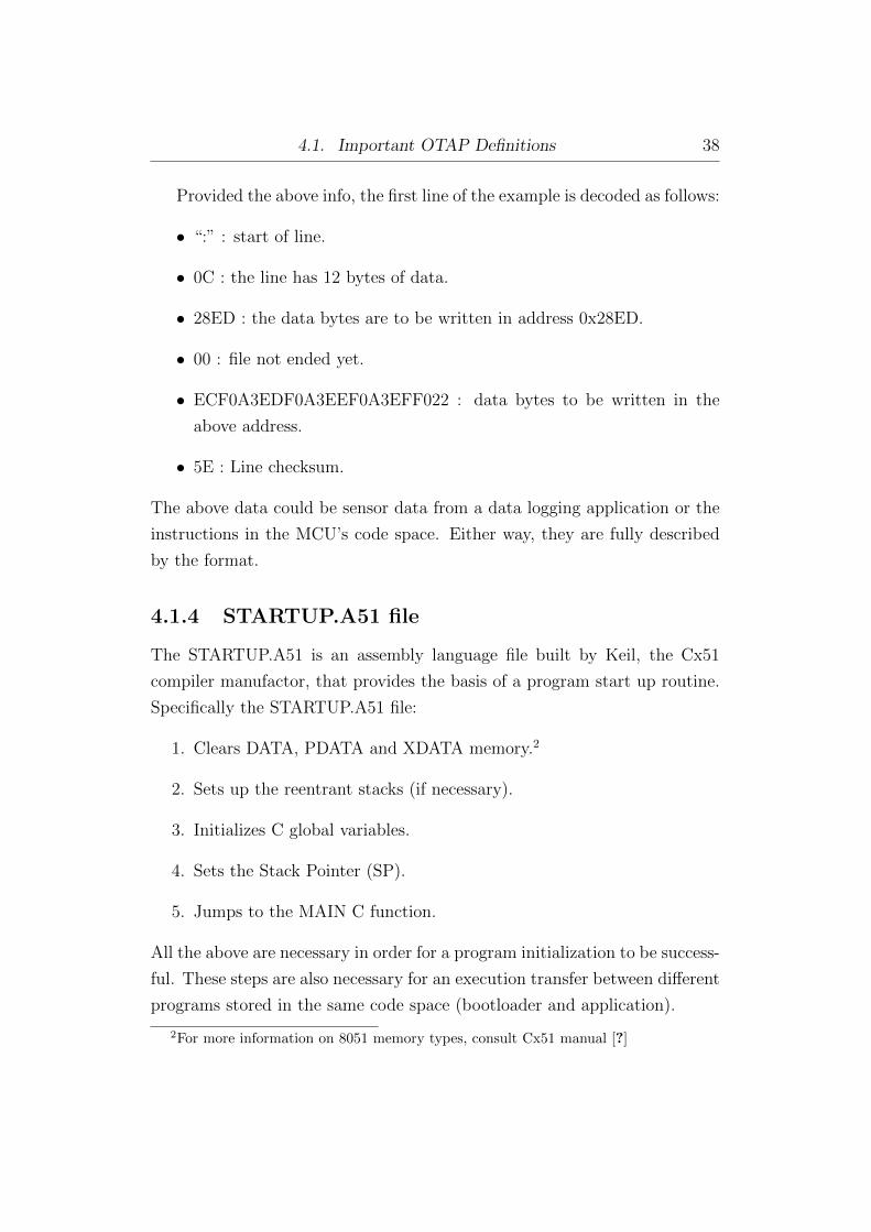
Provided the above info, the first line of the example is decoded as follows:
• “:” : start of line.
• 0C : the line has 12 bytes of data.
• 28ED : the data bytes are to be written in address 0x28ED.
• 00 : file not ended yet.
• ECF0A3EDF0A3EEF0A3EFF022 : data bytes to be written in the
above address.
• 5E : Line checksum.
The above data could be sensor data from a data logging application or the
instructions in the MCU’s code space. Either way, they are fully described
by the format.
4.1.4 STARTUP.A51 file
The STARTUP.A51 is an assembly language file built by Keil, the Cx51
compiler manufactor, that provides the basis of a program start up routine.
Specifically the STARTUP.A51 file:
1. Clears DATA, PDATA and XDATA memory.2
2. Sets up the reentrant stacks (if necessary).
3. Initializes C global variables.
4. Sets the Stack Pointer (SP).
5. Jumps to the MAIN C function.
All the above are necessary in order for a program initialization to be success-
ful. These steps are also necessary for an execution transfer between different
programs stored in the same code space (bootloader and application).
2For more information on 8051 memory types, consult Cx51 manual [?]
4.1. Important OTAP Definitions 39
4.1.5 XXXX.M51 file
The M51 file is a linker output file with information about the linking process
of a program. There is useful information contained in the file but basically
the information valuable for the OTAP process is the link map of the module.
In the link map, the following are quoted: the addresses of XDATA, DATA
data variables and CODE memory of the program’s functions, variables and
constants. It is useful for checking whether the setup of the application to be
downloaded and the bootloader are correct. For more information, consult
section “how to use OTAP”.
4.1.6 Interrupt vectors
When an interrupt occurs, the MCU saves its execution state and initiates
the execution of a code named “interrupt handler”. The interrupt handler is
mainly a piece of code that is executed whenever an interrupt occurs. The
memory address where the handler is saved is called an interrupt vector.
In the C8051F320 the interrupts are directed to the beginning of the code
space a.k.a code space address 0x000. For further information consult the
C8051F320 manual, interrupts section. As an example, if the external in-
terrupt 1 (INT1) occurs, the MCU will begin executing the code saved at
address 0x0013. After the interrupt handler finishes execution, the MCU
program counter is set to where the program stopped when the interrupt
occurred.
4.2. Middleware developed 40
4.2 Middleware developed
The OTAP project for the developed node is consisted out of four middleware
parts :
• The slave bootloader (installed in the node).
• The slave interrupt pseudo-handler (installed in the node).
• The slave user application (installed in the node, developed by user).
• The master firmware updater (installed in the gateway).
4.2.1 Bootloader
The bootloader is the middleware responsible for most of the work of the
OTAP. It is the middleware that receives the code wirelessly, writes it to flash
memory, checks its validity and starts the downloaded application. Moreover,
one of the most important characteristics of the loader is the ability to be
executed under any circumstances and application faults. That is possible
through a series of mechanisms that state the bootloader stable and always
executable. The program start is located in the code space address 0x100.
Described below are all of the important functions and capabilities of the
bootloader that make the OTAP possible.
Decode and download
Once started, the loader erases the predefined code space where the user
application will be stored. The next step is to wait for code to be received
wirelessly by using the receive code() function. This is the function that
receives and decodes the incoming Hex file. Below is a brief piece of code in
order for the user to understand how this function works.
4.2. Middleware developed 41
1 do{2 // ignore a l l c ha rac t e r s u n t i l reach ing the record mark f i e l d
3 while ( c = get key ( ) != ’ : ’ ){ ; }4 // ge t the record l en g t h
5 l en = get key ( ) ;
6 // ge t the MSB of the s t a r t i n g
7 // address ( o f f s e t f i e l d in HEX record )
8 o f f s e t = get key ( ) ;
9 // s h i f t the v a r i a b l e in order to save the LSB
10 o f f s e t <<= 8 ;
11 // ge t the LSB
12 o f f s e t |= get key ( ) ;
13 // ge t the record type
14 reco rd type = get key ( ) ;
15
16 // check the record type
17 i f ( r e co rd type != 0 && reco rd type != 1 ){18 // i f the record type i s not v a l i d
19 return CODE NOT VALID ;
20 }21
22 // i n i t a f l a s h po in t e r wi th the record ’ s o f f s e t
23 f l a s h p o i n t e r = o f f s e t ;
24
25 // wr i t e the data f i e l d o f the hex f i l e u n t i l a l l data ends
26 for ( i = 0 ; i < l en ; i++){27 i f ( f l a s h p o i n t e r < LAST FLASH ADDRESS){28 FLASH ByteWrite ( f l a s h p o i n t e r ++,get key ( ) ) ;
29 } else {30 // i f t h e r e i s a t r y to wr i t e in a non v a l i d address
31 return CODE NOT VALID ;
32 }33 }34
35 // i n i t a v a r i a b l e to check f o r checksum v a l i d i t y from f l a s h
36 f lash checksum = 0 ;
37 f l a s h p o i n t e r = o f f s e t ;
38 for ( i = 0 ; i < l en ; i++){39 // add the data f i e l d s t o r ed in FLASH to the checksum

4.2. Middleware developed 42
40 f lash checksum += FlashByteRead ( f l a s h p o i n t e r++) ;
41 }42
43 // ge t the HEX record checksum f i e l d
44 checksum = get key ( ) ;
45
46 // add the remaining f i e l d s
47 f lash checksum += len ;
48
49 // Take the s h i f t e d by 8 b i t s o f f s e t v a r i a b l e
50 // and add i t to the f l a sh checksum
51 //This i s done , in order to take on ly
52 // the 8 most s i g n i f i c a n t b i t s o f the v a r i a b l e
53 f lash checksum += (char ) ( o f f s e t >> 8) ;
54 // Mask the o f f s e t f i e l d in order to take the
55 // 8 l e a s t s i g n i f i c a n t b i t s o f the o f f s e t v a r i a b l e
56 f lash checksum += (char ) ( o f f s e t & 0x00FF) ;
57 // This i s done because f l a sh checksum va r i a b l e
58 // i s sma l l e r than the o f f s e t v a r i a b l e and adding
59 // w i l l l e ad to an ove r f l ow
60 f lash checksum += reco rd type ;
61 f lash checksum += checksum ;
62
63 // v e r i f y the checksum ( the f l a sh checksum shou ld equa l zero )
64 i f ( f lash checksum != 0){65 // i f checksum i s not v a l i d
66 return CODE NOT VALID ;
67 }68 }while ( r e co rd type != 1) ;
69
70 // i f EOF record type found re turn t ha t code i s v a l i d
71 return CODE VALID ;
4.2. Middleware developed 43
The above code depicts the main functionality of the receive code() func-
tion. To begin with, using this code, the Hex file is received character by
character and thus each line is fully decoded. Moreover, the code received is
stored in the addresses described in the “offset” field. Finally, a checksum-
type check is executed by reading the contents written in flash thus imple-
menting a test for flash corruption. In any case, if something interrupts the
above procedure, the byte stored in flash is already stated as not valid. For
example, if a power failure occurs, or a sudden reset for any reason, the boot-
loader will be the program to be executed and waiting for new code to be
downloaded and not the partially downloaded code.
Initialization and application boot
Mentioned above is that once the bootloader is started, a control code is
executed in order to verify the validity of the code currently in flash. This
code simply reads the validity variable from flash and if it is set, the user
application is executed. The execution of the code is done by using C function
pointers. A function pointer is a variable that points to the address of a
function. By using function pointers, it is possible to initiate a function
(or in this case a whole program) only by knowing the address where this
function is saved. The example below does exactly that (it is a code block
from the bootloader program):
1
2 //Dec lara t ion o f f unc t i on po in t e r to a p p l i c a t i o n
3 void (∗ a p p l i c a t i o n ) ( ) ;
4
5 //Raise the now running boot loader f l a g
6 PSW &= ! 0 x02 ;
7
8 //Read the v a l i d i t y by t e o f the code cu r r en t l y in f l a s h
9 v a l i d = FLASH ByteRead(CODE VALID ADDRESS) ;
10
11 // I f code i s v a l i d
12 //or the P1 3 a t tached but ton i s not pres sed
13 i f ( v a l i d == CODE VALID && P1 3 ){14
4.2. Middleware developed 44
15 // as s i gn the func t i on po in t e r
16 a p p l i c a t i o n = (void code ∗) APP ADDRESS;
17
18 // r a i s e the now running app f l a g
19 PSW |= 0x02 ;
20
21 // jump to the a p p l i c a t i o n i the f l a s h
22 a p p l i c a t i o n ( ) ;
23 }
In the case above, a function pointer of a function with void type of
return and no arguments is firstly declared. Then, a general purpose bit
from one of the microcontroller’s registers is set in order for the interrupts to
be directed correctly (see “pseudo interrupt vector” section). Finally, if the
code is characterized valid, the function pointer is used in order to jump to
the application’s main(). The code above depicts the described functionality
and is executed upon every MCU reset.
Moreover one can observe a more hardcoded check using the MCU’s P1 3
port. If this port is short-circuited with the ground pin of the MCU on reset,
whatever the validity bit, the execution is transferred to the bootloader pro-
gram. This functionality gives the user the ability to initiate the bootloader
at will, even if the application has stalled infinitely. For a more explanatory
scheme, see Fig. 4.3.
The use of function pointers was selected instead of in line assembly
because the compiler that was used did not have such capability (or at least in
a user friendly way). The Cx51 manual is equipped with further information
about function pointers.
4.2. Middleware developed 45
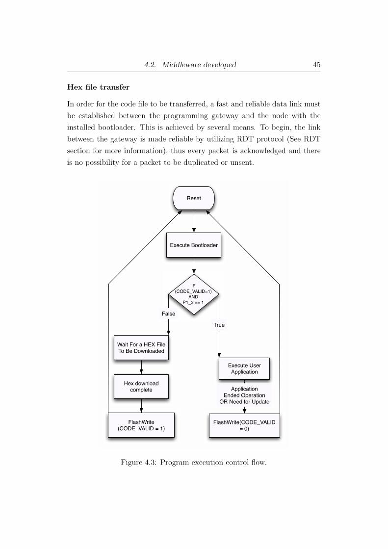
Hex file transfer
In order for the code file to be transferred, a fast and reliable data link must
be established between the programming gateway and the node with the
installed bootloader. This is achieved by several means. To begin, the link
between the gateway is made reliable by utilizing RDT protocol (See RDT
section for more information), thus every packet is acknowledged and there
is no possibility for a packet to be duplicated or unsent.
Reset
IF
(CODE_VALID=1)
AND
P1_3 == 1
False
Wait For a HEX File To Be Downloaded
Execute User Application
True
FlashWrite(CODE_VALID = 0)
Application Ended Operation
OR Need for Update
Hex download complete
FlashWrite(CODE_VALID = 1)
Execute Bootloader
Figure 4.3: Program execution control flow.
4.2. Middleware developed 46
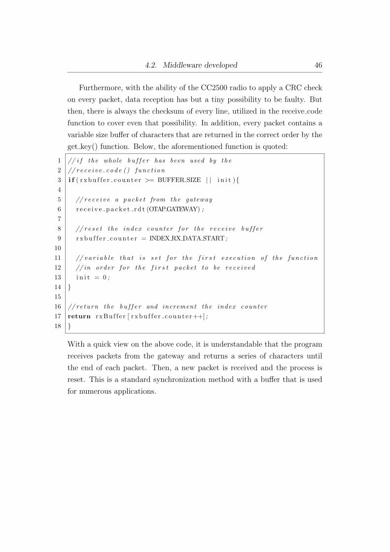
Furthermore, with the ability of the CC2500 radio to apply a CRC check
on every packet, data reception has but a tiny possibility to be faulty. But
then, there is always the checksum of every line, utilized in the receive code
function to cover even that possibility. In addition, every packet contains a
variable size buffer of characters that are returned in the correct order by the
get key() function. Below, the aforementioned function is quoted:
1 // i f the whole b u f f e r has been used by the
2 // r e c e i v e cod e ( ) f unc t i on
3 i f ( r x b u f f e r c o u n t e r >= BUFFER SIZE | | i n i t ){4
5 // r e c e i v e a packe t from the gateway
6 r e c e i v e p a c k e t r d t (OTAPGATEWAY) ;
7
8 // r e s e t the index counter f o r the r e c e i v e b u f f e r
9 r x b u f f e r c o u n t e r = INDEX RX DATA START ;
10
11 // v a r i a b l e t ha t i s s e t f o r the f i r s t execu t i on o f the func t i on
12 // in order f o r the f i r s t packe t to be r e c e i v ed
13 i n i t = 0 ;
14 }15
16 // re turn the b u f f e r and increment the index counter
17 return rxBuf f e r [ r x b u f f e r c o u n t e r++] ;
18 }
With a quick view on the above code, it is understandable that the program
receives packets from the gateway and returns a series of characters until
the end of each packet. Then, a new packet is received and the process is
reset. This is a standard synchronization method with a buffer that is used
for numerous applications.
4.2. Middleware developed 47
4.2.2 User application
The user application is the code to be downloaded using the bootloader. The
bootloader, as stated above is responsible to jump to this address in order
to begin the program execution. The application code has almost no limi-
tations regarding functionality, meaning that every module of the MCU can
be used, as if the bootloader does not exist. The two programs are executed
completely independently. In order to make the application downloadable,
the user must set the application code to begin from an address declared
APP ADDRESS in the “bootloader.h” library (default value 0x1000). In
addition, the user has to set up the interrupt vectors to begin at address
APP ADDRESS and set up the STARTUP.A51 file to jump to the address
APP ADDRESS in order for the main function to start (more information
in “how to use OTAP” section).
There are certain limitations regarding the memory use of the applica-
tion. First and foremost, the application, should not overwrite the boot-
loader code in any way. The address where the loader is saved is stated in
the corresponding .M51 file. If a flash write occurs to the bootloader code
space, the download operation would be stated error prone and the whole
system would be faulty and difficult to debug. Furthermore, the application
should not write to a flash address beyond LAST FLASH PAGE (default
value 0x3BFF) as declared in the bootloader.h library. In this memory bank
valuable information is stored, such as the MAC ADDRESS of the node and
the code validity bit. Finally, taking into account the previous limitations,
the amount of flash memory available for application code is limited to 11263
Bytes (and not 16KBytes) due to the fact that the application code starts in
address 0x1000 and ends at most at 0x3BFF. Of course this is a minor draw-
back because the typical application memory size varies from 2 to 6 KBytes
and at most 10 KBytes of code.
To conclude, a piece of code must be added into the application which,
when executed, initiates the bootloader. That way, the OTAP process can
be initiated without physical contact with the node. For example, the node
could be programmed in such way, that when a special packet is received the
4.2. Middleware developed 48
bootloader is started, in order for a new application to be downloaded. The
code sequence with which the bootloader is started, within the application
code is shown :
1 //Write to the f l a s h memory t ha t the code i s not v a l i d
2
3 FLASH ByteWrite (CODE VALID ADDRESS, CODE NOT VALID) ;
4 // Sof tware r e s e t
5 RSTSRC = 0x10 ;
When the above code is executed, the node execution is transferred in
OTAP mode and awaits for a program to be downloaded wirelessly. The
first instruction unsets the validity of the code. Therefore, upon reset, the
bootloader, after checking this variable’s value, is initiated (for more info
check the bootloader section). This way, the code execution can be trans-
ferred from the application to the bootloader and a new program can be
downloaded.
4.2.3 Interrupt pseudo-vector
As quoted in the interrupt vector section, when an interrupt occurs, the
MCU automatically jumps to the corresponding interrupt vector. In the case
of the particular OTAP project, when an interrupt occurs, the execution is
transferred to a program that selects whether to direct the interrupt to the
bootloader, or to the downloaded user application interrupt service routine.
The program is named interrupt pseudo-vector, because it is not actually
an interrupt vector but a control program in order for the interrupts to be
directed correctly. The selection of which program’s ISR will be executed is
done by using the “F1” bit from the C8051F320 register “PSW”. If this bit
is set, the application is the one that is currently running and the interrupt
is directed to it, otherwise, it is handled by the bootloader. A code part of
the pseudo-vector is depicted below:
4.2. Middleware developed 49
1 ; DownLoader base address
2 DnlBase Equ 0100H
3 ; App l i ca t i on base address
4 AppBase Equ 1000H
5
6 ; S t a r t Loader
7 CSEG AT 0
8 Ljmp DnlBase
9
10 ; INT0 − Externa l I n t e r rup t
11 CSEG AT 3
12 JB PSW. 1 , InterruptV0
13 Ajmp DnlBase+(3)
14 InterruptV0 :
15 Ljmp AppBase+(3)
16
17 ;T0 − Timer 0 In t e r rup t
18 CSEG AT 8∗1+3
19 JB PSW. 1 , InterruptV1
20 Ajmp DnlBase +(11)
21 InterruptV1 :
22 Ljmp AppBase+(11)
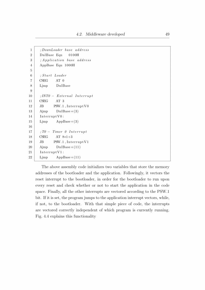
The above assembly code initializes two variables that store the memory
addresses of the bootloader and the application. Followingly, it vectors the
reset interrupt to the bootloader, in order for the bootloader to run upon
every reset and check whether or not to start the application in the code
space. Finally, all the other interrupts are vectored according to the PSW.1
bit. If it is set, the program jumps to the application interrupt vectors, while,
if not, to the bootloader. With that simple piece of code, the interrupts
are vectored correctly independent of which program is currently running.
Fig. 4.4 explains this functionality
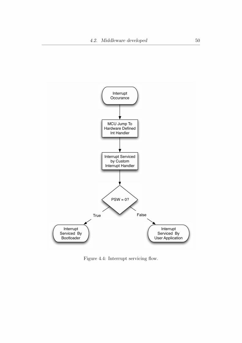
4.2. Middleware developed 50
Interrupt Occurance
MCU Jump To Hardware Defined
Int Handler
PSW = 0?
Interrupt Serviced By Bootloader
Interrupt Serviced By
User Application
True False
Interrupt Serviced by Custom
Interrupt Handler
Figure 4.4: Interrupt servicing flow.
4.2. Middleware developed 51
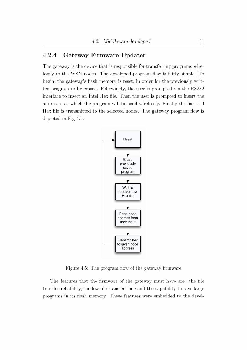
4.2.4 Gateway Firmware Updater
The gateway is the device that is responsible for transferring programs wire-
lessly to the WSN nodes. The developed program flow is fairly simple. To
begin, the gateway’s flash memory is reset, in order for the previously writ-
ten program to be erased. Followingly, the user is prompted via the RS232
interface to insert an Intel Hex file. Then the user is prompted to insert the
addresses at which the program will be send wirelessly. Finally the inserted
Hex file is transmitted to the selected nodes. The gateway program flow is
depicted in Fig 4.5.
Reset
Erase previously saved program
Wait to receive new Hex file
Read node address from user input
Transmit hex to given node address
Figure 4.5: The program flow of the gateway firmware
The features that the firmware of the gateway must have are: the file
transfer reliability, the low file transfer time and the capability to save large
programs in its flash memory. These features were embedded to the devel-
4.2. Middleware developed 52
oped firmware with the utilization of a series of mechanisms and techniques.
The following section summarizes the functionality of the programming gate-
way.
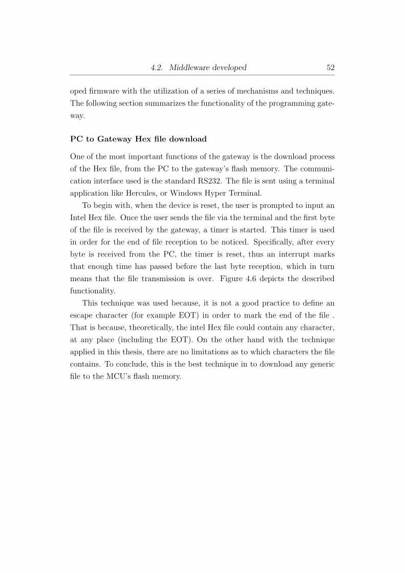
PC to Gateway Hex file download
One of the most important functions of the gateway is the download process
of the Hex file, from the PC to the gateway’s flash memory. The communi-
cation interface used is the standard RS232. The file is sent using a terminal
application like Hercules, or Windows Hyper Terminal.
To begin with, when the device is reset, the user is prompted to input an
Intel Hex file. Once the user sends the file via the terminal and the first byte
of the file is received by the gateway, a timer is started. This timer is used
in order for the end of file reception to be noticed. Specifically, after every
byte is received from the PC, the timer is reset, thus an interrupt marks
that enough time has passed before the last byte reception, which in turn
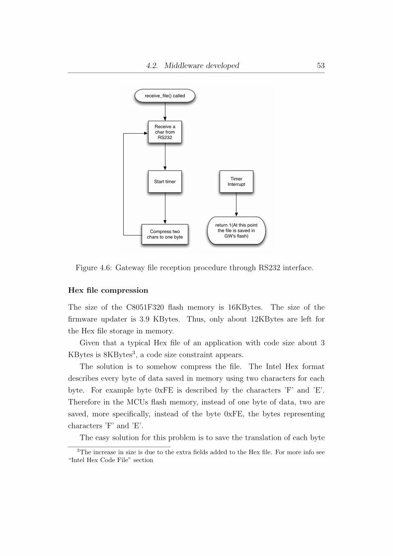
means that the file transmission is over. Figure 4.6 depicts the described
functionality.
This technique was used because, it is not a good practice to define an
escape character (for example EOT) in order to mark the end of the file .
That is because, theoretically, the intel Hex file could contain any character,
at any place (including the EOT). On the other hand with the technique
applied in this thesis, there are no limitations as to which characters the file
contains. To conclude, this is the best technique in to download any generic
file to the MCU’s flash memory.
4.2. Middleware developed 53
Receive a char from RS232
Start timerTimer Interrupt
return 1(At this point the file is saved in
GW's flash)
receive_file() called
Compress two chars to one byte
Figure 4.6: Gateway file reception procedure through RS232 interface.
Hex file compression
The size of the C8051F320 flash memory is 16KBytes. The size of the
firmware updater is 3.9 KBytes. Thus, only about 12KBytes are left for
the Hex file storage in memory.
Given that a typical Hex file of an application with code size about 3
KBytes is 8KBytes3, a code size constraint appears.
The solution is to somehow compress the file. The Intel Hex format
describes every byte of data saved in memory using two characters for each
byte. For example byte 0xFE is described by the characters ’F’ and ’E’.
Therefore in the MCUs flash memory, instead of one byte of data, two are
saved, more specifically, instead of the byte 0xFE, the bytes representing
characters ’F’ and ’E’.
The easy solution for this problem is to save the translation of each byte
3The increase in size is due to the extra fields added to the Hex file. For more info see“Intel Hex Code File” section

4.2. Middleware developed 54
from ASCII characters to actual binary data. To begin, once a character
is received from the RS232 interface, it is converted to its representation as
an integer number with the utilization of the toInt() function. For example,
the character ‘F’ is converted to the number 15 and the string “FE” to the
number 254. The number 254 can be stored in a variable that is 8 bits
long, whereas the string “FE” needs 16 bits of memory space. After the
received character is converted, a counter indicating the number of received
characters is incremented(in Fig. 4.7 it is named byte num). If the counter
value is an even number, the converted character is saved to the lower 4 bits
of an 8 bit buffer and if it is odd, to the higher 4 bits. The separation is done
by dividing the counter with 2 and taking the remainder. If it is zero, the
counter is an even number, otherwise it is an odd number. This way, pairs of
characters are saved in the correct order and only one byte instead of two is
used, thus a 2:1 compression ratio is achieved. After each pair is compressed,
the buffer that stores the converted number, is saved to the flash memory,
and the procedure is repeated until the end of the file.
With the Hex file compression utilization, the file storage capability of
the gateway is virtually doubled and therefore, more complex and larger
programs can be stored and transferred wirelessly to the WSN. Figure 4.7
depicts this functionality.
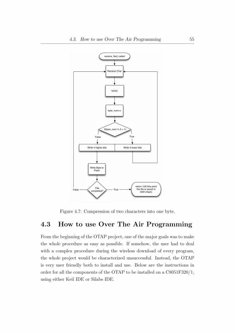
4.3. How to use Over The Air Programming 55
if(byte_num % 2 = 1)
Write 4 higher bits Write 4 lower bits
toInt()
byte_num++
Write Byte to Flash
File completed?
return 1(At this point the file is saved in
GW's flash)
receive_file() called
Receive Char
False True
False True
Figure 4.7: Compression of two characters into one byte.
4.3 How to use Over The Air Programming
From the beginning of the OTAP project, one of the major goals was to make
the whole procedure as easy as possible. If somehow, the user had to deal
with a complex procedure during the wireless download of every program,
the whole project would be characterized unsuccessful. Instead, the OTAP
is very user friendly both to install and use. Below are the instructions in
order for all the components of the OTAP to be installed on a C8051F320/1,
using either Keil IDE or Silabs IDE.

4.3. How to use Over The Air Programming 56
4.3.1 Files needed and their description
The OTAP project consists of a number of source files that are necessary for
a succesfull compilation and operation. The files are separated in 3 different
folders:
• The common libs folder, which is used for the firmware updater and
the bootloader libraries and source files.
• The “bootloader” folder is used for the libraries and the source file
containing the main() function of the bootloader.
• The firmware updater folder which is used for the libraries and the
source file containing the main() function of the firmware updater.
4.3.2 Setting up the application to be bootload-able
1. Write the application code, as normal.
2. Relocate the code of the application as per the corresponding the boot-
loader.h, APP ADDRESS definition (default 0x1000). Do this by us-
ing the CODE(“address”) directive. For example, for the default set
up linking command would be :
“BL51.EXE TEST APPLICATION.obj, TO application CODE (1000H)”
In Keil uVision IDE from main menu goto: Project → Options
for Target → “BL51locate” tab → Change the “Code” textfield to
APP ADDRESS value(default 1000H).
In Silicon Labs IDE : from main menu goto: Project →Tool Chain
Integration→ “Linker” tab→ “Customize” button→ Change the “Code
Address” textfield to APP ADDRESS value(default 0x1000).
3. Include in the application’s compilation files the STARTUP.A51 file.
Keil strongly recommends that every program should include this file,
in uVision and SiLabs IDEs this is done automatically. The file is lo-
cated at $KeilCompilerInstallationFolder$\C51\LIB\STARTUP.A51.
4.3. How to use Over The Air Programming 57
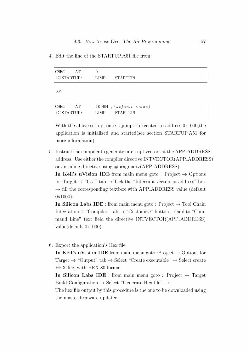
4. Edit the line of the STARTUP.A51 file from:
CSEG AT 0
?C STARTUP: LJMP STARTUP1
to:
CSEG AT 1000H ; ( d e f a u l t va lue )
?C STARTUP: LJMP STARTUP1
With the above set up, once a jump is executed to address 0x1000,the
application is initialized and started(see section STARTUP.A51 for
more information).
5. Instruct the compiler to generate interrupt vectors at the APP ADDRESS
address. Use either the compiler directive INTVECTOR(APP ADDRESS)
or an inline directive using #pragma iv(APP ADDRESS).
In Keil’s uVision IDE from main menu goto : Project → Options
for Target→ “C51” tab→ Tick the “Interrupt vectors at address” box
→ fill the corresponding textbox with APP ADDRESS value (default
0x1000).
In Silicon Labs IDE : from main menu goto : Project→ Tool Chain
Integration→ “Compiler” tab→ “Customize” button→ add to “Com-
mand Line” text field the directive INTVECTOR(APP ADDRESS)
value(default 0x1000).
6. Export the application’s Hex file:
In Keil’s uVision IDE from main menu goto :Project→ Options for
Target→ “Output” tab→ Select “Create executable”→ Select create
HEX file, with HEX-80 format.
In Silicon Labs IDE : from main menu goto : Project → Target
Build Configuration → Select “Generate Hex file” →The hex file output by this procedure is the one to be downloaded using
the master firmware updater.
4.3. How to use Over The Air Programming 58
All the above may seem like a lot of work to be done. On the contrary, the
whole procedure does not take more than a minute and it has to be done
only once per project.
4.3.3 Setting up and Installing the bootloader
1. In the bootloader.h library set up the MAC ADDRESS field. This is
the node’s mac address in order to receive the Intel Hex file from the
gateway.
2. Include STARTUP.A51 into the code files.
3. Set up the STARTUP.A51 to jump to address 0x100.
4. Select a MAC ADDRESS from 0 to 255 in library Link.h.
5. Set up the interrupt vectors to begin at address 0x100.
6. Compile the bootloader.
7. Download the executable.
Once all the above are done, the WSN node is ready to receive code
wirelessly. Upon reset, the bootloader is executed and waits for code to be
received.
4.3.4 Using master firmware updater to program over
the air
1. Compile and download the firmware updater to a RS232 interface com-
patible node.
2. Connect the gateway to a working RS232 connector.
3. Open a COM terminal (for example Hercules or Hyper Terminal).
4. Turn on the device.
5. Insert the application’s Intel Hex file to the COM terminal.4
4In Hercules, right-click→Insert file. In Hyper Terminal use the “send” button
4.3. How to use Over The Air Programming 59
6. Select a range of MAC addresses for the code to be downloaded. For
example an input of 3 to 5 will download the saved program to the
nodes with MAC addresses 3 to 5 starting the download from number
3. If the user wants to deliver the application only to node 5, number
5 shall be inserted twice etc.
7. If the message is : “Download completed successfully” then the target
node was programmed successfully. Otherwise, programming was not
successful. If the programming is not successful then the node shall
reset after a timeout and wait for new code download.
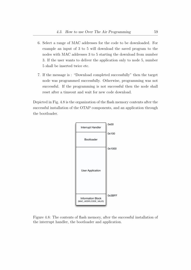
Depicted in Fig. 4.8 is the organization of the flash memory contents after the
successful installation of the OTAP components, and an application through
the bootloader.
Information Block(MAC_ADDR,CODE_VALID)
Interrupt Handler
Bootloader
User Application
0x100
0x00
0x1000
0x3BFF
Figure 4.8: The contents of flash memory, after the successful installation ofthe interrupt handler, the bootloader and application.

4.3. How to use Over The Air Programming 60
4.3.5 Over The Air Programmed “Blinky” Demo
(“Hello World” example)
This section will cover the setup and installation of all the OTAP compo-
nents described above, including a simple bootload-able application. The
application’s functionality is the blinking of one of the node’s LED.
Interrupt pseudo-vector setup
1. Start Keil uVision IDE.
2. Create a new project named “interrupt vector project”.
3. Select from the database the C8051F320 MCU from Silicon Laborato-
ries.
4. Click no to the pop up menu with the question: “Copy Standard 8051
Startup Code to Project Folder and Add to Project?”.
5. Copy the “Interrupt handler.a” file in the project folder.
6. Expand the folder “Target 1” in the Project Workspace.
7. Right click the “Source Group 1” folder and select the “Add files to
Group” option.
8. From the drop down menu “Files of type” select “Asm Source files”.
9. Add the “Interrupt handler.a” file which is included with the files of
this thesis.
10. Close the file explorer.
11. Build the target using the corresponding button.
12. Connect a device utilizing the C8051F320 MCU using the SiLabs Debug
Adapter.
13. Download the code.

4.3. How to use Over The Air Programming 61
Bootloader
1. Without closing the Keil uVision IDE instance created for the interrupt
vector setup, open another instance of the IDE.
2. Create a new project named “Bootloader project”.
3. Make sure that the project will be saved in a folder other than the
Interrupt vector’s project folder.
4. Copy all the files included in the “common libs” and the “bootloader”
folder in the project folder.
5. With the same steps as above, add all the files that where included in
“common libs” folder except:
• “receive packet csma.c”
• “send packet csma.c”
• “sleep.c”
• “channel clear.c”
6. Add all the files that where included in the “bootloader” folder.
7. Set up the MAC address of the node (constant MAC ADDRESS in
Link.h library) to be the value 1.
8. Relocate the code of the bootloader:
From the main menu, go to: Project→Options for Target→ “BL51locate”
tab → Change the “Code” textfield to 100H.
9. Copy the STARTUP.A51 file into the project folder. The file is located
at $KeilCompilerInstallationFolder$\C51\LIB\STARTUP.A51.
10. Add the STARTUP.A51 to the project files.
11. Edit the line of the STARTUP.A51 file from:
4.3. How to use Over The Air Programming 62
CSEG AT 0
?C STARTUP: LJMP STARTUP1
to:
CSEG AT 100H ;
?C STARTUP: LJMP STARTUP1
12. Set up the interrupt vectors:
From main menu go to : Project → Options for Target → “C51” tab
→ Tick the “Interrupt vectors at address” box→ fill the corresponding
textbox with the value 0x100.
13. Download the code. In the pop up menu with the question:
“Erase memory contents” select NO. If the contents of the flash
memory are erased, the interrupt pseudo-vector must be reinstalled.
Application
1. Without closing the Keil uVision IDE instance created for the interrupt
vector and the bootloader setup, open another instance of the IDE.
2. Create a new project named “Application project”.
3. Create a new text file using a text editor and copy the code cited in
the appendix.
4. Save the file under the name “Bootloadable Blinky.c”.
5. Copy the file into the project folder.

4.3. How to use Over The Air Programming 63
6. Copy the files listed below from the “common libs” folder into the
project folder:
• “compiler defs.h”
• “C8051F320 defs.h”
• “FlashPrimitives.h”
• “F320 FlashPrimitives.c”
7. Add the above files to the compilation list, using the steps described
above.
8. Relocate the code of the application:
From the main menu, go to: Project→Options for Target→ “BL51locate”
tab → Change the “Code” textfield to 1000H.
9. Copy the STARTUP.A51 file into the project folder. The file is located
at $KeilCompilerInstallationFolder$\C51\LIB\STARTUP.A51.
10. Add the STARTUP.A51 to the project files.
11. Edit the line of the STARTUP.A51 file from:
CSEG AT 0
?C STARTUP: LJMP STARTUP1
to:
CSEG AT 1000H ;
?C STARTUP: LJMP STARTUP1
12. Set up the interrupt vectors:
From main menu go to : Project → Options for Target → “C51” tab
→ Tick the “Interrupt vectors at address” box→ fill the corresponding
textbox with the value 0x1000.

4.3. How to use Over The Air Programming 64
13. Export the application’s Hex file:
From the main menu go to: Project→ Options for Target→ “Output”
tab→ Select “Create executable”→ Select create HEX file, with HEX-
80 format.
14. Build the project using the corresponding button. The “Application project.hex”
hex file is the one to be downloaded using OTAP.
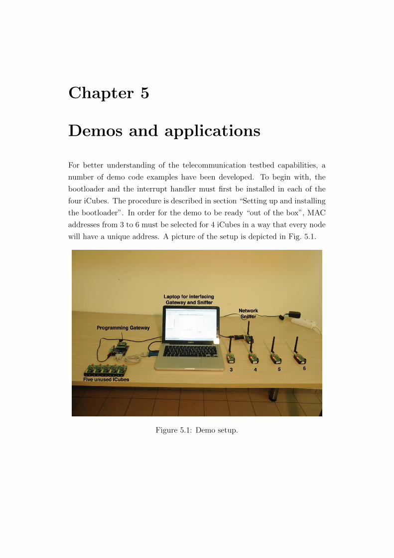
Chapter 5
Demos and applications
For better understanding of the telecommunication testbed capabilities, a
number of demo code examples have been developed. To begin with, the
bootloader and the interrupt handler must first be installed in each of the
four iCubes. The procedure is described in section “Setting up and installing
the bootloader”. In order for the demo to be ready “out of the box”, MAC
addresses from 3 to 6 must be selected for 4 iCubes in a way that every node
will have a unique address. A picture of the setup is depicted in Fig. 5.1.
Figure 5.1: Demo setup.
Chapter 5. Demos and applications 66
Moreover, the gateway firmware must be installed to a device utilizing
the C8051F320/1 (such as the iCube or the C8051F320DK) and connected
to a PC running a UART terminal. The host PC must have the Keil 8051
toolchain installed. In section “Setting up the application to be bootload-
able”, the steps in order for the demos to be bootload-able are listed.
Code-wise, the demo.c and demo config.h are the main files of the demo.
The functionality of the demos is contained in the demo.c file. The code
utilizes the preprocessor by using the “#ifdef” instruction, in order to select
one out of 5 different demo applications. The selection is made by uncom-
menting the corresponding line in the demo config.h library. This way code
size optimization is achieved. Furthermore, the demo application is designed
in a way that the user will be required to compile and install only once for
each demo.
Finally, a technique is presented in order for the application to enter
bootloading mode under all circumstances. For this purpose, a timer is
utilized (specifically, timer3). The timer is initiated to interrupt every half a
second. Then, the application is responsible to count the interrupts and select
a threshold (TIMEOUT RESET) after which it executes the bootloader.
This way, even if the application has entered an endless loop or even crashed,
OTAP will always be available, either from the normal application procedure,
or from the timer3 interrupt handler (which in some demos below is selected
as the only way to enter bootloading mode).
Chapter 5. Demos and applications 67
5.0.6 Application Description
A brief description of the six different demos is depicted below.
Led blinking (“Hello World”)
This is a simple LED blinking application. After all the initializations, the
system enters a “for loop” with iterations selected from the ITERATIONS
definition. Furthermore, a wait interval between each blinking is selected us-
ing the WAIT TIME definition. After the iterations have surpassed, the ap-
plication enters the bootloading mode by using the ENTER BOOTLOADER
macro, defined in bootloading essentials.h. The results of the application
with a default set up of the iCube would be for the LED to blink for a num-
ber of times described in ITERATIONS and enter bootloading mode. This
demo is selected by uncommenting the line “#define LED” in demo config.h.
Bidirectional relay system
The purpose of this application is the demonstration of the simplicity with
which a reliable multihop system that can transfer data from one point to
another. The simplicity is referred in terms of code, because the multi-
hop WSN code in this example requires mainly 40 lines of code, since RDT
routines are already developed. Once the application is downloaded in all
four iCube nodes, a blinking LED from every iCube node, indicates the
data direction from the first set up node to the last one (RIGHT RELAY
and LEFT RELAY utilize opposite directions). After a number of timer3
interrupts have occurred, the application executes the macro to return to
bootloading mode. The selection of the demo is done by uncommenting ei-
ther the line “#define RIGHT RELAY” or the “#define LEFT RELAY” in
demo config.h. Figure 5.2 depicts a relay demo execution. One can observe
the packet propagation through the relays, since for every successfull packet
transmission a LED is turned on.
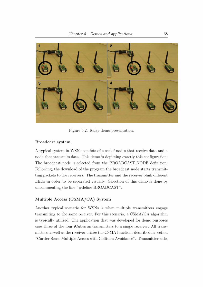
Chapter 5. Demos and applications 68
Figure 5.2: Relay demo presentation.
Broadcast system
A typical system in WSNs consists of a set of nodes that receive data and a
node that transmits data. This demo is depicting exactly this configuration.
The broadcast node is selected from the BROADCAST NODE definition.
Following, the download of the program the broadcast node starts transmit-
ting packets to the receivers. The transmitter and the receiver blink different
LEDs in order to be separated visually. Selection of this demo is done by
uncommenting the line “#define BROADCAST”.
Multiple Access (CSMA/CA) System
Another typical scenario for WSNs is when multiple transmitters engage
transmiting to the same receiver. For this scenario, a CSMA/CA algorithm
is typically utilized. The application that was developed for demo purposes
uses three of the four iCubes as transmitters to a single receiver. All trans-
mitters as well as the receiver utilize the CSMA functions described in section
“Carrier Sense Multiple Access with Collision Avoidance”. Transmitter-side,
Chapter 5. Demos and applications 69
packets are being send between random time intervals. After a succesfull
packet transmission has been achieved (acknowledgement received), a LED
blinking occurs. Receiver-side, the node is always in receive mode and ac-
cepts packets from all mac addresses and returns ACKS to the corresponding
nodes while blinking a LED when a reception was succesful. The performance
of the demo is not optimal because timeout fine tuning was not performed
as this code is only a proof of concept demo for the OTAP.
5.0.7 Network debugging tool
During the development of the telecommunication testbed, there was need
for recording and logging the packet streams throughout the network. For
the purposes of this task, firmware for packet sniffing was developed. With
the utilization of the packet sniffer, the packet flow can be recorded, thus the
telecommunication engineer is reinforced with a valuable network debugging
and data logging tool.
The functionality of the sniffer is fairly simple. The WSN node equipped
with the sniffer firmware, utilizes the primitive function of packet reception
in order to receive every transmitted packet of the network. The packet
information is saved in an array. Particularly, the type, the transmitter and
receiver of the packet are stored and presented to the user for further analysis.
Followingly, the instructions for the operation of the packet sniffer are
depicted. To start with, the user must first install the firmware to a WSN
node capable of communicating with a PC using a RS232 interface. After
the installation, and the initialization of the sniffer node, the user will be
prompted to start the packet reception by sending a special character through
the interface (default is ‘b’). At this stage the user should start the operation
of the network and begin the packet sniffing. If a number of packets defined
in PACKET BUFFER SIZE definition are received, or user inserts character
‘s’, the packet sniffing is stopped and the information of the collected packets
are presented to the user. Below, an example of the printouts of the network
debugging tool is depicted:
Fig. 5.3 depicts the sniffer printouts after the successful reception of 10
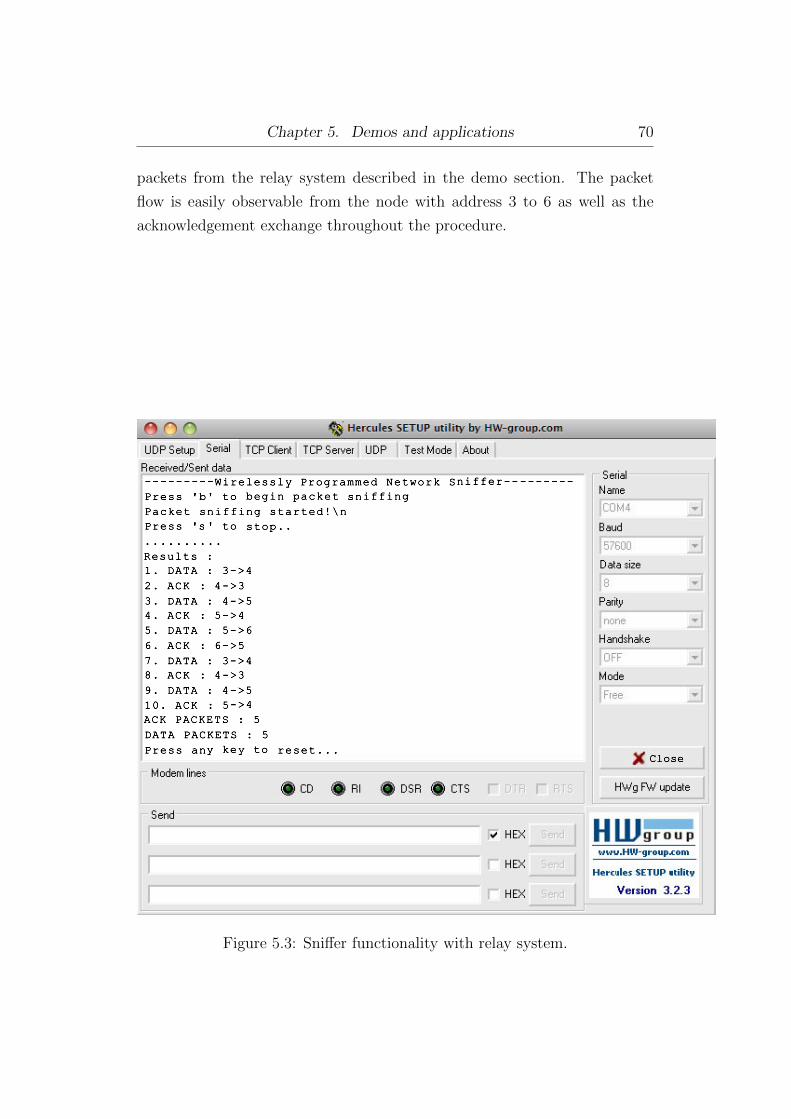
Chapter 5. Demos and applications 70
packets from the relay system described in the demo section. The packet
flow is easily observable from the node with address 3 to 6 as well as the
acknowledgement exchange throughout the procedure.
Figure 5.3: Sniffer functionality with relay system.

Chapter 6
Conclusion and future/ongoing
work
6.1 Future/Ongoing Work
For this thesis, a OTAP methodology was developed from scratch. The main
components developed throughout the thesis are the Over The Air Program-
ming capability, the XTboard, the Reliable Data Transmission routines and
the programs that demonstrate the testbed potential.
There is a lot of ongoing and future work in order for the WSN under
development to be an even more competitive product compared to prior art.
The projects that are either programmed for future work or currently under
development are summarized below.
iCube2
The iCube2 is a future project that involves the design and implementation
of a new wireless sensor network node. The new node will consist of a more
advanced and lower power consumption MCU, which utilizes modules such
as a Real Time Clock that provide the engineer with further functionalities
and capabilities.

6.1. Future/Ongoing Work 72
Ultra low power OTAP
Currently, Over The Air Programming is a fairly high power consuming pro-
cedure. Speciffically, when the node is receiving code wirelessly consumes
around 80mW of power. The power consumption of the process can be
reduced to the order of a few hundreds microwatts by utilizing “Wake On
Radio”, “Periodic Sleep” and other techniques for minimizing the power con-
sumption of a WSN node. Such techniques shall be applied to the OTAP in
the future.
Multihop OTAP
The developed OTAP is currently capable of programming nodes that are
within the range of the gateway, i.e within one hop. This is a critical con-
straint for a wirelessly programmed WSN. For this reason, multihop OTAP
capability is currently under development in order to overcome this con-
straint. Multihop OTAP will be based on the same principles with the one
already developed, with the addition of a packet routing or flooding technique
that will enable the programming of nodes with no access to the gateway.
Energy Harvesting
Energy harvesting is the process with which energy derived from external
sources is captured, and stored into energy containers such as batteries or
ultra capacitors. Such energy sources are the sun rays, the wind or even RF
power from ambient signals (such as UHF). For the exploitation of these envi-
ronmental energy soirces, special modules are currently under development.
The modules include boost converters [7], rectennas [8], custom wind-mills [9]
and utilization of advanced energy storage solutions, such as those in [10].
6.2. Challenges during development 73
6.2 Challenges during development
During the development of all the above middleware and hardware there were
certain problems. Some were critical for the development process and others
minor. Both are stated below.
The most important of the problems was the lack of a usable debug-
ger for networking applications. The debugger provided by Silicon Labs,
unfortunately is neither easy to use nor capable of debugging networking
applications. Therefore all the debugging procedures where done utilizing
LED blinking, oscilloscopes and UART printouts (which for most bugs do
not work). The above debugging tools are clearly not sufficient for a devel-
oper that needs to know exactly what is happening with interrupts and the
contents of the flash memory in real time while packets are being received
and sent wirelessly.
Another critical challenge was the lack of the the fact that OTAP appli-
cation was developed from ground up using custom primitive functions and
trial-and-error practices. This process helped a lot to educate the author and
to develop an application that is fresh and easily updatable.
Moreover, from the beginning of the OTAP project, a challenge was to
set up three different applications to be installed in the same memory. For
the purposes of this challenge, the whole project was separated into three
different Keil uVision IDE sub-projects which were edited and installed si-
multaneously. This means that three different projects had to be debugged,
set up and installed as one. If one of these was buggy, everything failed.
For example, if the pseudo-interrupt vector did not redirect the interrupts
correctly, then a difficult to find bug would appear either on the bootloader,
or in the application.

6.3 Conclusion
The telecommunication testbed developed is a high quality engineering tool
for the fast deployment of research projects and applications. The capability
of remote WSN programming is available through a simple installation and
deployment process, thus providing the engineer the ability to update the
network within seconds. Moreover, the XTboard is an essential interfacing
tool for the iCubes node in order for the latter to be transformed to a fully
functional sensor node capable of transferring data to a PC. Finally, the
demos described in section “Demos and Applications” speed up the learning
process of the tool and are used to demonstrate the capabilities of the testbed.
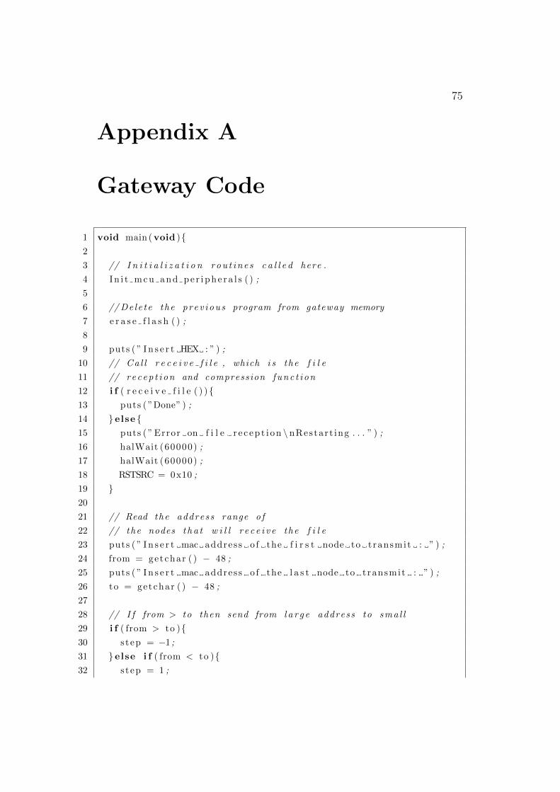
75
Appendix A
Gateway Code
1 void main (void ){2
3 // I n i t i a l i z a t i o n rou t i n e s c a l l e d here .
4 I n i t m c u a n d p e r i p h e r a l s ( ) ;
5
6 //De le te the prev ious program from gateway memory
7 e r a s e f l a s h ( ) ;
8
9 puts ( ” I n s e r t HEX : ” ) ;
10 // Ca l l r e c e i v e f i l e , which i s the f i l e
11 // recep t i on and compression func t i on
12 i f ( r e c e i v e f i l e ( ) ){13 puts ( ”Done” ) ;
14 } else {15 puts ( ” Error on f i l e r e c e p t i o n \ nRestar t ing . . . ” ) ;
16 halWait (60000) ;
17 halWait (60000) ;
18 RSTSRC = 0x10 ;
19 }20
21 // Read the address range o f
22 // the nodes t ha t w i l l r e c e i v e the f i l e
23 puts ( ” I n s e r t mac address o f the f i r s t node to transmit : ” ) ;
24 from = getchar ( ) − 48 ;
25 puts ( ” I n s e r t mac address o f the l a s t node to transmit : ” ) ;
26 to = getchar ( ) − 48 ;
27
28 // I f from > to then send from l a r g e address to sma l l
29 i f ( from > to ){30 step = −1 ;
31 } else i f ( from < to ){32 step = 1 ;

Appendix A. Gateway Code 76
33 } else {34 step = 1 ;
35 }36
37 puts ( ”\nTransmitt ing f i l e . ” ) ;
38 for ( node num = from //
39 ; node num != to+s t ep //
40 ; node num = node num+s t ep ){41
42 // p r i n t ou t
43 putchar ( node num + ’ 0 ’ ) ;
44 putchar ( ’ \n ’ ) ;
45
46 // Here t r a n sm i t f i l e i s c a l l e d
47 // This f unc t i on u t i l i z e s the RDT f u n c t i o n a l i t y
48
49 i f ( t r a n s m i t f i l e ( (UINT8) node num )){50 puts ( ”\nTransmition Success ! ” ) ;
51 } else {52 // I f t ransmiss ion f a i l e d , r e s e t
53 puts ( ”\nTransmit Fa i l ed !\n” ) ;
54 RSTSRC = 0x10 ;
55 }56 }57
58 // I f a l l nodes have r e c e i v ed the f i l e , r e s e t
59 puts ( ”\ nResett ing . . . \ n” ) ;
60 RSTSRC = 0x10 ;
61 }
77
Appendix B
Blinky code
1 //−−−−−−−−−−−−−−2 // F320 Blinky . c
3 //−−−−−−−−−−−−−−4 // This program f l a s h e s the green LED on the
5 //C8051F32x t a r g e t board .
6 // Af ter the LED b l i n k i n g the node execu t i on i s t r an s f e r e d
7 // in boo t l oad ing mode .
8
9
10 //−−−−−−−−−−−−−−11 // Inc lude s
12 //−−−−−−−−−−−−−−13
14 #include ” . . / common libs / c o m p i l e r d e f s . h”
15 #include ” . . / common libs / C8051F320 defs . h”
16 #include ” . . / common libs / F320 FlashPr imit ives . h”
17
18 //−−−−−−−−−−−−−−19 // Globa l CONSTANTS
20 //−−−−−−−−−−−−−−21
22 #define UPDATER ADDRESS 0x100
23 #define CODE VALID ADDRESS 0x3BFF
24
25 // LED1=’1 ’ means ON
26 SBIT(LED1, SFR P2 , 7) ;
27 // LED2=’1 ’ means ON
28 SBIT(LED2, SFR P2 , 6) ;
29
30 //−−−−−−−−−−−−−−31 // Function PROTOTYPES
32 //−−−−−−−−−−−−−−
Appendix B. Blinky code 78
33
34 void SYSCLK Init (void ) ;
35 void PORT Init (void ) ;
36 void halWait ( int t imeout ) ;
37
38
39 //−−−−−−−−−−−−−−40 // MAIN Routine
41 //−−−−−−−−−−−−−−42
43 void main (void )
44 {45 int i ;
46 // Disab l e watchdog t imer
47 PCA0MD &= ˜0x40 ;
48 // r a i s e the now running app f l a g
49 PSW |= 0x02 ;
50 // I n i t i a l i z e system c l o c k
51 SYSCLK Init ( ) ;
52 // I n i t i a l i z e c ro s s bar and GPIO
53 PORT Init ( ) ;
54
55 while (1){56
57 while (1){ ; }58 for ( i = 0 ; i < 25 ; i++){59 halWait (40000) ;
60 LED1 = !LED1 ;
61 }62
63
64 //Unset the code v a l i d i t y b i t
65 FLASH ByteWrite (CODE VALID ADDRESS , 0) ;
66 // So f t r e s e t
67 RSTSRC = 0x10 ;
68
69
70 }71
Appendix B. Blinky code 79
72 }73 // Delay func t i on
74 void halWait ( int t imeout ) {75 do {76 nop ( ) ;
77 nop ( ) ;
78 nop ( ) ;
79 nop ( ) ;
80 nop ( ) ;
81 nop ( ) ;
82 nop ( ) ;
83 nop ( ) ;
84 nop ( ) ;
85 nop ( ) ;
86 nop ( ) ;
87 nop ( ) ;
88 nop ( ) ;
89 nop ( ) ;
90 } while (−−t imeout ) ;
91 }// halWait
92
93 //−−−−−−−−−−−−−−94 // SYSCLK Init
95 //−−−−−−−−−−−−−−96 void SYSCLK Init (void )
97 {98 // Conf igure i n t e r n a l o s c i l l a t o r f o r
99 OSCICN = 0x80 ;
100 // Enable miss ing c l o c k d e t e c t o r
101 RSTSRC = 0x04 ;
102 }103
104 //−−−−−−−−−−−−−−105 // PORT Init
106 //−−−−−−−−−−−−−−107 void PORT Init (void )
108 {109 // Enable P2 6 as a push−p u l l output
110 P2MDOUT |= 0x40 ;
Appendix B. Blinky code 80
111 // Enable P2 7 as a push−p u l l output
112 P2MDOUT |= 0x80 ;
113
114 // Enable c ro s s bar and weak pu l l−ups115 XBR1 = 0x40 ;
116 }117
118 //−−−−−−−−−−−−−−119 // End Of F i l e
120 //−−−−−−−−−−−−−−
81
Appendix C
Demo codes
C.1 LED Blinking
1 #ifde f LED
2 #define SPAM WAIT 20000
3 #define ITERATIONS 100
4 #define TIMEOUT RESET 1000
5 for ( i = 0 ; i < ITERATIONS ; i++){6 halWait (SPAM WAIT) ;
7 BLINK6 ;
8 }9 START BOOTLOADER( ) ;
10 #endif
C.2 Relay system with direction from node
6 to 3
1 #ifde f RIGHT RELAY
2 #define SPAM WAIT 30000
3 #define TIMEOUT RESET 700
4 while (1){5
6 i f (mac == TX1){7 //SPAMWAIT∗6 r e s u l t s in an ove r f l ow
8 // thus 6 c a l l s o f halWait are used
9 halWait (SPAM WAIT) ;
10 halWait (SPAM WAIT) ;
11 halWait (SPAM WAIT) ;
12 halWait (SPAM WAIT) ;
C.2. Relay system with direction from node 6 to 3 82
13 halWait (SPAM WAIT) ;
14 halWait (SPAM WAIT) ;
15 i f ( RDTsend packet rdt (RX1)){16 ON6;
17 halWait (SPAM WAIT) ;
18 OFF6 ;
19 }20 }21
22 i f (mac == RX1){23 i f ( RDTrece ive packet rdt (TX1, 2 0 ) ){24 halWait (SPAM WAIT) ;
25 i f ( RDTsend packet rdt (TX2)){26 ON6;
27 halWait (SPAM WAIT) ;
28 OFF6 ;
29 }30 }31 }32
33 i f (mac == TX2){34 i f ( RDTrece ive packet rdt (RX1, 2 0 ) ){35 halWait (SPAM WAIT) ;
36 i f ( RDTsend packet rdt (RX2)){37 ON6;
38 halWait (SPAM WAIT) ;
39 OFF6 ;
40 }41 }42 }43
44 i f (mac == RX2){45
46 i f ( RDTrece ive packet rdt (TX2, 2 0 ) ){47 halWait (SPAM WAIT) ;
48 ON6;
49 halWait (SPAM WAIT) ;
50 OFF6 ;
51 }
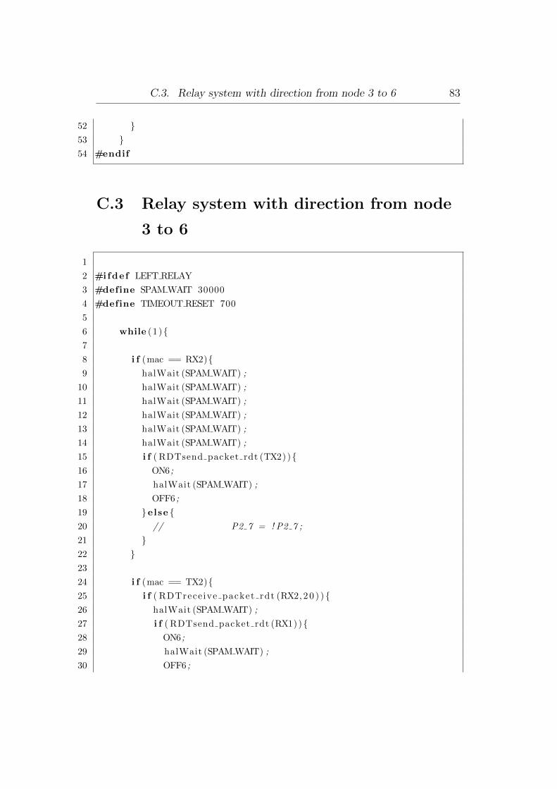
C.3. Relay system with direction from node 3 to 6 83
52 }53 }54 #endif
C.3 Relay system with direction from node
3 to 6
1
2 #ifde f LEFT RELAY
3 #define SPAM WAIT 30000
4 #define TIMEOUT RESET 700
5
6 while (1){7
8 i f (mac == RX2){9 halWait (SPAM WAIT) ;
10 halWait (SPAM WAIT) ;
11 halWait (SPAM WAIT) ;
12 halWait (SPAM WAIT) ;
13 halWait (SPAM WAIT) ;
14 halWait (SPAM WAIT) ;
15 i f ( RDTsend packet rdt (TX2) ){16 ON6;
17 halWait (SPAM WAIT) ;
18 OFF6 ;
19 } else {20 // P2 7 = ! P2 7 ;
21 }22 }23
24 i f (mac == TX2){25 i f ( RDTrece ive packet rdt (RX2, 2 0 ) ){26 halWait (SPAM WAIT) ;
27 i f ( RDTsend packet rdt (RX1)){28 ON6;
29 halWait (SPAM WAIT) ;
30 OFF6 ;
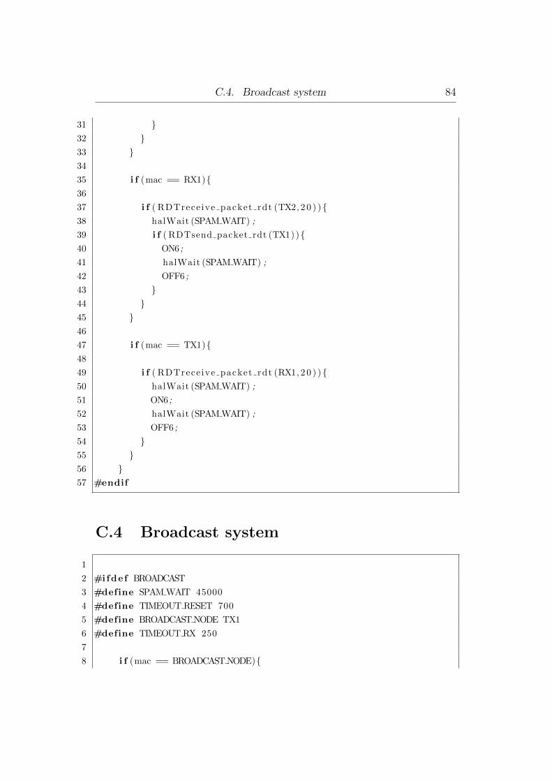
C.4. Broadcast system 84
31 }32 }33 }34
35 i f (mac == RX1){36
37 i f ( RDTrece ive packet rdt (TX2, 2 0 ) ){38 halWait (SPAM WAIT) ;
39 i f ( RDTsend packet rdt (TX1)){40 ON6;
41 halWait (SPAM WAIT) ;
42 OFF6 ;
43 }44 }45 }46
47 i f (mac == TX1){48
49 i f ( RDTrece ive packet rdt (RX1, 2 0 ) ){50 halWait (SPAM WAIT) ;
51 ON6;
52 halWait (SPAM WAIT) ;
53 OFF6 ;
54 }55 }56 }57 #endif
C.4 Broadcast system
1
2 #ifde f BROADCAST
3 #define SPAM WAIT 45000
4 #define TIMEOUT RESET 700
5 #define BROADCAST NODE TX1
6 #define TIMEOUT RX 250
7
8 i f (mac == BROADCAST NODE){
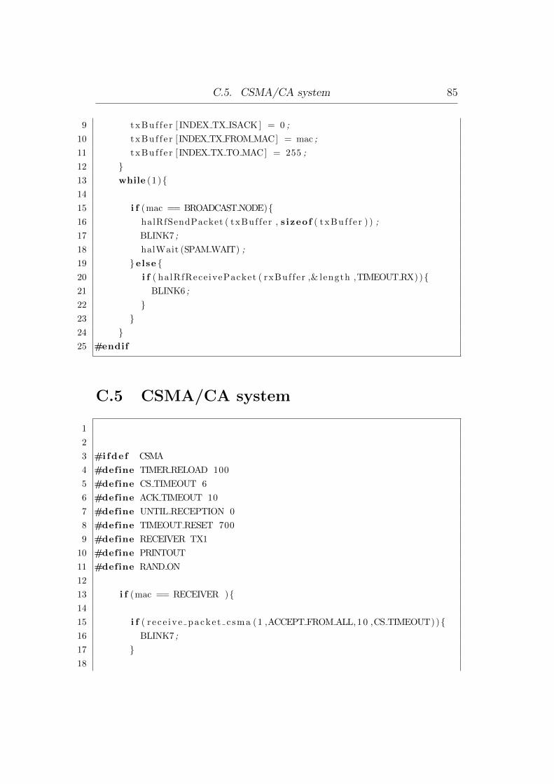
C.5. CSMA/CA system 85
9 txBuf f e r [ INDEX TX ISACK ] = 0 ;
10 txBuf f e r [INDEX TX FROM MAC] = mac ;
11 txBuf f e r [ INDEX TX TO MAC] = 255 ;
12 }13 while (1){14
15 i f (mac == BROADCAST NODE){16 halRfSendPacket ( txBuf fer , s izeof ( txBuf f e r ) ) ;
17 BLINK7 ;
18 halWait (SPAM WAIT) ;
19 } else {20 i f ( halRfRece ivePacket ( rxBuf fer ,& length ,TIMEOUT RX)){21 BLINK6 ;
22 }23 }24 }25 #endif
C.5 CSMA/CA system
1
2
3 #ifde f CSMA
4 #define TIMER RELOAD 100
5 #define CS TIMEOUT 6
6 #define ACK TIMEOUT 10
7 #define UNTIL RECEPTION 0
8 #define TIMEOUT RESET 700
9 #define RECEIVER TX1
10 #define PRINTOUT
11 #define RAND ON
12
13 i f (mac == RECEIVER ){14
15 i f ( r e c e i v e packe t c sma (1 ,ACCEPT FROM ALL, 1 0 ,CS TIMEOUT)){16 BLINK7 ;
17 }18
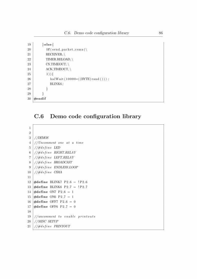
C.6. Demo code configuration library 86
19 } else {20 i f ( send packet csma (\21 RECEIVER,\22 TIMER RELOAD,\23 CS TIMEOUT,\24 ACK TIMEOUT,\25 1)){26 halWait (10000∗ ( (BYTE) rand ( ) ) ) ;
27 BLINK6 ;
28 }29 }30 #endif
C.6 Demo code configuration library
1
2
3 //DEMOS
4 //Uncomment one at a time
5 //#de f i n e LED
6 //#de f i n e RIGHT RELAY
7 //#de f i n e LEFT RELAY
8 //#de f i n e BROADCAST
9 //#de f i n e ENDLESS LOOP
10 //#de f i n e CSMA
11
12 #define BLINK7 P2 6 = ! P2 6
13 #define BLINK6 P2 7 = ! P2 7
14 #define ON7 P2 6 = 1
15 #define ON6 P2 7 = 1
16 #define OFF7 P2 6 = 0
17 #define OFF6 P2 7 = 0
18
19 //uncomment to enab l e p r i n t ou t s
20 //MISC SETUP
21 //#de f i n e PRINTOUT

87
Bibliography
[1] Silicon Laboratories homepage. http://www.silabs.com.
[2] Waspmote mote datasheet. http://www.libelium.com/
documentation/waspmote/waspmote-datasheet_eng.pdf.
[3] Isense mote datasheet. http://www.coalesenses.com/download/
data_sheets/DS_CM30X_1v0.pdf.
[4] Lotus mote datasheet. http://www.memsic.com/support/
documentation/wireless-sensor-networks/category/
7-datasheets.html?download=186%3Alotus.
[5] Iris mote datasheet. http://www.memsic.com/support/
documentation/wireless-sensor-networks/category/
7-datasheets.html?download=135%3Airis.
[6] List of wireless sensor nodes. http://en.wikipedia.org/wiki/List_
of_wireless_sensor_nodes#List_of_sensor_nodes.
[7] Boost converter definition. http://en.wikipedia.org/wiki/Boost_
converter.
[8] Rectenna definition. http://en.wikipedia.org/wiki/Rectenna.
[9] Custom windmill url. http://www.telecom.tuc.gr/~aggelos/
tel412_fall2010/project4.html.
[10] Infinity batteries homepage. http://www.infinitepowersolutions.
com/products/thinergy.
[11] Silabs ”C8051F320/1” manual. http://www.silabs.com/Support%
20Documents/TechnicalDocs/C8051F32x.pdf.

Bibliography 88
[12] Texas instruments ”CC2500” manual. http://www.ti.com/lit/ds/
symlink/cc2500.pdf.
[13] Tinyos rtos homepage. www.tinyos.net.
[14] Eagle pcb design software homepage. http://www.cadsoftusa.com/.
[15] National instruments ”LM2937” manual. http://www.national.com/
mpf/LM/LM2937-3.3.html#Overview.
[16] Sipex ”SP3223” manual. http://www.datasheetcatalog.org/
datasheet/sipex/SP3243CT.pdf.
[17] Telosb mote datasheet. http://www.willow.co.uk/TelosB_
Datasheet.pdf.
[18] Btnode mote datasheet. http://www.btnode.ethz.ch/pub/files/
btnode_rev3.22_productbrief.pdf.
[19] Micaz mote datasheet. http://www.openautomation.net/
uploadsproductos/micaz_datasheet.pdf.
[20] A.Bletsas, A. Vlachaki, E. Kampianakis, G. Sklivanitis, J. Kimionis,
K. Tountas, M. Asteris, and P. Markopoulos. Building the low-cost
digital garden as a telecom lab exercise. IEEE Pervasive Computing,
Accepted. to appear in 2012.
[21] A. Bletsas, A. Vlachaki, E. Kampianakis, G. Sklivanitis, J. Kimionis,
K. Tountas, M. Asteris, and P. Markopoulos. Towards precision agricul-
ture: Building a soil wetness multi-hop wsn from first principles. April
2011. Second International Workshop in Sensing Technologies in Archi-
tecture, Forestry and Environment(ECOSENSE) 2011.
[22] James F. Kurose and Keith W. Ross. Computer Networking. Addison-
Wesley, Reading, Massachusetts, 2010.


