
Complementary wireless module WLAN / BT
Standard Laminate SiP Module
Series/Type: R078 (WL1831) / D7025 Ordering code: B30921D7025Y918
Date: 2014-09-25 Version: 1.2
Content of header bars 1 and 2 of data sheet will be automatically entered in headers and footers! Please fill in the table and then change the color to "white". This ensures that the table disappears (invisible) for the customer PDF. Don't change formatting when entering or pasting text in the table and don't add any cell or line in and to it!
Identification/Classification 1 (header 1 + top left bar):
Complementary wireless module WLAN / BT
Identification/Classification 2 (header 2 + bottom left header bar):
Standard Laminate SiP Module
Ordering code: (top right header bar) B30921D7025Y918
Series/Type: (bottom right header bar) R078 (WL1831) / D7025
Preliminary data (optional): (if necessary)
Department: SAW IT
Date: 2014-09-25
Version: 1.2
EPCOS AG 2015. Reproduction, publication and dissemination of this publication, enclosures hereto and the information contained therein without EPCOS' prior express consent is prohibited.
EPCOS AG is a TDK Group Company.

Complementary wireless module WLAN / BT B30921D7025Y918
Standard Laminate SiP Module R078 (WL1831) / D7025
SAW IT 2014-09-25
Please read Cautions and warnings and Page 2 of 48 Important notes at the end of this document.
1 Overview This document details the specifications and features of R078 (WL1831) / D7025 SiP module. The R078 (WL1831) / D7025 SiP module is based on Texas Instruments WL1831 IC, specifically WL183x Data Sheet version 1.4, such that the SiP module specification is subject to any subsequent changes in applicable Texas Instruments documentation and software. The R078 (WL1831) / D7025 contains the WL1831 SoC, 2.4GHz SPDT switches, 2.4GHz band pass filters / diplexer and necessary passive components for WLAN and BT in a highly integrated solution.
1.1 Features
WLAN, BT, BLE on a single chip provide universal connectivity in small PCB footprint.
Provides efficient direct connection to battery by employing several integrated switched mode power supplies (DC2DC).
Based on 45nm CMOS technology using proven core technology.
Seamless integration with TI OMAP™ Application Processors.
WLAN and Bluetooth cores software and hardware are compatible with prior WL127x and WL128x offerings, for smooth migration to Device.
Shared HCI transport for BT/BLE over UART and SDIO for WLAN.
Downloadable patches and firmware enables new features to be added for all functional block's.
Temperature detection and compensation mechanism ensures minimal variation in the RF performance over the entire temperature range.
Bluetooth 4.0, BLE and all audio processing features work in parallel and include full coexistence with WLAN
1.2 Applications
Mobile phone and mobile computer device applications.
1.3 General Description
The R078 (WL1831) / D7025 is a highly integrated WLAN, BT, BLE device that forms a complete standalone communication system. The WL1831 is a highly integrated single-chip CMOS (45-nm process) incorporates the core functionality of the WL1271/3 and WL1281/3 devices.
The device is the 8th-generation WLAN/BT/BLE devices from Texas Instruments. As such, the WL1831 is based upon proven core technology and complements the TI integrated devices for connectivity portfolio.
R078 (WL1831) / D7025 is ideal for use in mobile phone and mobile computer device applications due to its low current, small area and cellular phone coexistence-friendly features.
Complementary wireless module WLAN / BT B30921D7025Y918
Standard Laminate SiP Module R078 (WL1831) / D7025
SAW IT 2014-09-25
Please read Cautions and warnings and Page 3 of 48 Important notes at the end of this document.
1.4 Terms and abbreviations
BPF – Band-Pass Filter
BT – Bluetooth
FE – Front-End (refers to FE IC and BPF)
GND – Ground
HCI – Host Controller Interface
IC – Integrated Circuit
I/O – Input/Output interfaces
LDO – Low Drop-Out (voltage regulator)
PCB – Printed Circuit Board
Q – Quality factor
RF – Radio Frequency
RX – Receive
SiP – System in Package
SoC – System on Chip
TX – Transmit
Vbat – Battery Voltage
VIO – external pre-existing 1.8V IO power supply
WLAN – Wireless Local Area Network
1.5 Reference documents
Texas Instruments WL183x_Data_Manual_Rev_1_4.pdf

Complementary wireless module WLAN / BT B30921D7025Y918
Standard Laminate SiP Module R078 (WL1831) / D7025
SAW IT 2014-09-25
Please read Cautions and warnings and Page 4 of 48 Important notes at the end of this document.
1 OVERVIEW ................................................................................................................................................................... 2
1.1 FEATURES ................................................................................................................................................................ 2
1.2 APPLICATIONS.......................................................................................................................................................... 2
1.3 GENERAL DESCRIPTION ........................................................................................................................................... 2
1.4 TERMS AND ABBREVIATIONS .................................................................................................................................... 3
1.5 REFERENCE DOCUMENTS ......................................................................................................................................... 3
2 FUNCTIONAL BLOCK FEATURES ......................................................................................................................... 5
2.1 FUNCTIONAL BLOCK DIAGRAM ............................................................................................................................... 5
2.2 WLAN FEATURES ................................................................................................................................................... 6
2.3 BLUETOOTH FEATURES ............................................................................................................................................ 6
2.4 BLE FEATURES ........................................................................................................................................................ 6
3 DETAILED DESCRIPTION ........................................................................................................................................ 7
3.1 HOST INTERFACES.................................................................................................................................................... 7
3.2 CLOCKS AND POWER MANAGEMENT ..................................................................................................................... 11
3.3 WLAN FUNCTIONAL BLOCK ................................................................................................................................. 15
3.4 BLUETOOTH FUNCTIONAL BLOCK ......................................................................................................................... 16
3.5 TERMINAL ASSIGNEMENTS .................................................................................................................................... 18
3.6 TERMINAL FUNCTIONS ........................................................................................................................................... 19
4 DESIGN GOAL SPECIFICATIONS ......................................................................................................................... 25
4.1 GENERAL CHIP REQUIREMENTS AND OPERATION .................................................................................................. 25
4.2 WLAN RF PERFORMANCE .................................................................................................................................... 28
4.3 BLUETOOTH RF PERFORMANCE ............................................................................................................................. 30
4.4 BLE RF PERFORMANCE ......................................................................................................................................... 34
4.5 INTERFACE TIMING CHARACTERISTICS .................................................................................................................. 36
4.6 PACKAGE MECHANICAL DRAWING ........................................................................................................................ 40
4.7 SCHEMATIC ............................................................................................................................................................ 41
5 LEAD-FREE PRODUCT STATUS ........................................................................................................................... 42
6 RECOMMENDED REFLOW PROFILE ................................................................................................................. 43
7 PACKING INFORMATION ...................................................................................................................................... 44
8 REVISION HISTORY................................................................................................................................................. 47
DISPLAY OF ORDERING CODES FOR EPCOS PRODUCTS .................................................................................... 47
Complementary wireless module WLAN / BT B30921D7025Y918
Standard Laminate SiP Module R078 (WL1831) / D7025
SAW IT 2014-09-25
Please read Cautions and warnings and Page 5 of 48 Important notes at the end of this document.
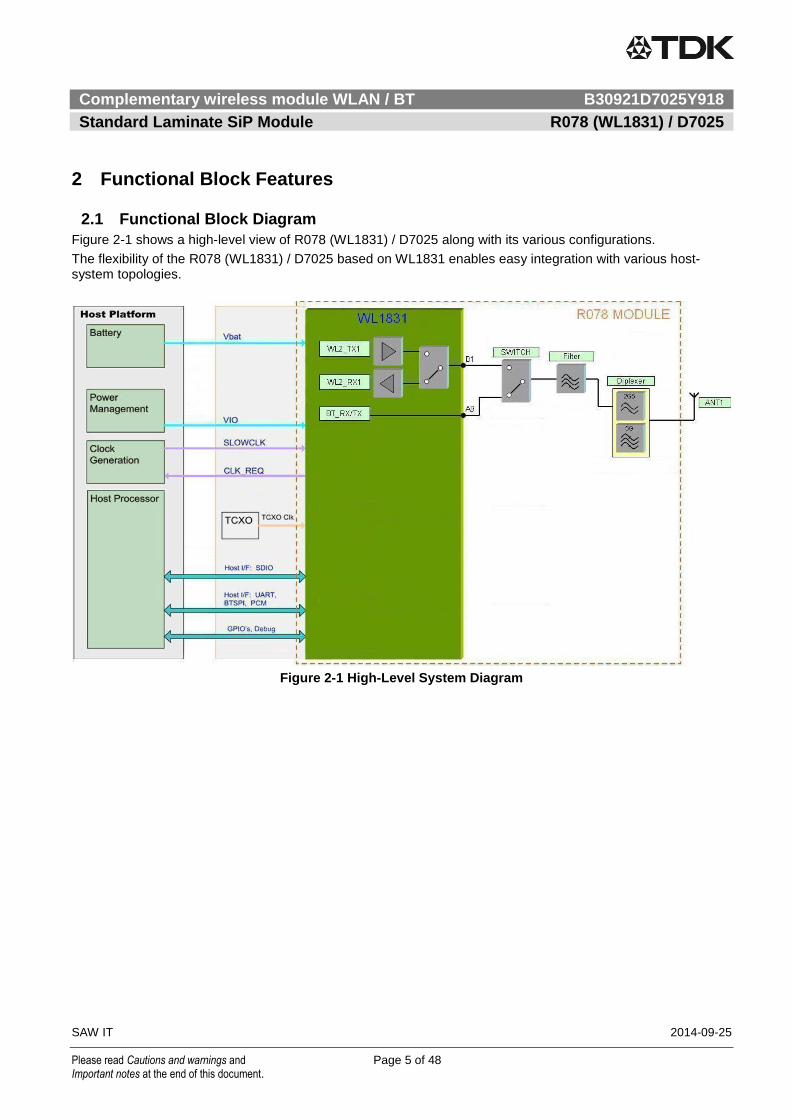
2 Functional Block Features
2.1 Functional Block Diagram
Figure 2-1 shows a high-level view of R078 (WL1831) / D7025 along with its various configurations.
The flexibility of the R078 (WL1831) / D7025 based on WL1831 enables easy integration with various host-system topologies.
Figure 2-1 High-Level System Diagram
Complementary wireless module WLAN / BT B30921D7025Y918
Standard Laminate SiP Module R078 (WL1831) / D7025
SAW IT 2014-09-25
Please read Cautions and warnings and Page 6 of 48 Important notes at the end of this document.
2.2 WLAN Features
Integrated 2.4GHz power amplifiers for complete WLAN solution
WLAN MAC Baseband Processor and RF transceiver - IEEE802.11b/g/n compliant
WLAN 2.4 GHz SISO (20 / 40 MHz channels).
Baseband Processor
IEEE Std 802.11b/g data rates and IEEE Std 802.11n data rates with 20 or 40 MHz SISO.
Fully calibrated system. No production calibration required.
Medium-Access Controller (MAC)
Embedded ARM™ Central Processing Unit (CPU)
Hardware-Based Encryption/Decryption Using 64-, 128-, and 256-Bit WEP, TKIP or AES Keys,
Supports requirements for Wi-Fi Protected Access (WPA and WPA2.0) and IEEE Std 802.11i
[Includes Hardware-Accelerated Advanced-Encryption Standard (AES)]
Designed to work with IEEE Std 802.1x
New advanced co-existence scheme with BT/BLE
2.4GHz Radio
Internal LNA, PA and RF switch
Supports: IEEE Std 802.11b, 802.11g and 802.11n
Supports 4 bit SDIO host interface, including high speed (HS) and V3 modes
2.3 Bluetooth Features
Supports Bluetooth 4.0 BLE
Includes concurrent operation and built-in coexistence and prioritization handling of BT, BLE, audio processing and WLAN
Dedicated Audio processor supporting on chip SBC encoding + A2DP:
Assisted A2DP (A3DP) support - SBC Encoding implemented internally
Assisted WB-Speech (AWBS) support - modified SBC codec implemented internally
2.4 BLE Features
Fully compliant with BT4.0 BLE dual mode standard
Support for all roles and role-combinations, mandatory as well as optional
Supports up to 10BLE connection
Independent buffering for LE allows having large number of multiple connections without affecting BR/EDR performance

Complementary wireless module WLAN / BT B30921D7025Y918
Standard Laminate SiP Module R078 (WL1831) / D7025
SAW IT 2014-09-25
Please read Cautions and warnings and Page 7 of 48 Important notes at the end of this document.
3 Detailed Description
3.1 Host Interfaces
3.1.1 Device Host Interface Options
The following table summarizes the Host Controller interface options. All interfaces operate independently.
Table 3-1 Host Controller Interface options
WLAN Shared HCI for
BT
BT Voice/Audio
WLAN HS SDIO Over UART BT PCM
The Device incorporates UART module dedicated to the BT shared-transport Host Controller Interface (HCI) transport layer. The HCI interface is used to transport commands, events, and ACL between the Bluetooth device and its host using HCI data packets.
This acts as a shared transport for BT/BLE functional blocks.
3.1.2 WLAN SDIO Transport Layer
The SDIO is the host interface for WLAN. The interface between the host and the D7025 uses an SDIO interface and supports a maximum clock rate of 50MHz.
The Device SDIO also supports the following features of the SDIO V3 specification:
4 bit data bus
Synchronous and Asynchronous In-Band-Interrupt
Default and High-Speed (50MHz) timing
Sleep/wake commands
SDIO timing specifications are given in specification section at end of document.
3.1.3 HCI UART Shared Transport Layers for BT
The HCI UART supports most baud rates (including all PC rates) for all fast clock frequencies - up to maximum of 4 Mbps. After power up the baud rate is set for 115.2 kbps, irrespective of fast clock frequency. The baud rate can then be changed by using a VS command. The Device responds with a Command Complete Event (still at 115.2 kbps), after which the baud rate change takes place.
HCI hardware includes the following features:
Receiver detection of break, idle, framing, FIFO overflow, and parity error conditions.
Transmitter underflow detection.
CTS/RTS hardware flow control.
4 wire (H4)
Table 3-2 UART Default Setting
Parameter Value
Bit rate 115.2 kbps
Data length 8 bits
Stop bit 1
Parity None

Complementary wireless module WLAN / BT B30921D7025Y918
Standard Laminate SiP Module R078 (WL1831) / D7025
SAW IT 2014-09-25
Please read Cautions and warnings and Page 8 of 48 Important notes at the end of this document.
3.1.3.1 UART 4 Wire Interface - H4
The interface includes four signals: TXD, RXD, CTS and RTS. Flow control between the host and the Device is byte-wise by hardware.
Flow control is obtained by the following:
Figure 3-1 HCI UART Connection
When the RX buffer of the Device passes the “flow control” threshold, it will set the HCI_RTS signal high to stop transmission from the host.
When the CTS signal is set high, the Device will stop its transmission on the interface. In case CTS is set high in the middle of transmitting a byte, the Device will finish transmitting the byte and stop the transmission.
3.1.3.2 BT function Firmware Low Power Mode Protocols
The Device includes a mechanism that handles the transition between operating mode and deep sleep low-power mode. The protocol is done via the UART and is known as eHCILL (enhanced HCI Low Level) power management protocol.
This protocol is backward compatible with the TI BT HCILL Protocol, so a Host that implements the HCILL does not need to change anything in order to work with the Device. The "Enhanced" portion of the HCILL introduces changes that allow a simpler host implementation of this protocol.
See SWRA288 eHCILL Four-Wire Power Management Protocol.
3.1.4 BT Audio CODEC Interface
3.1.4.1 Overview
The CODEC interface is a fully dedicated programmable serial port, supporting the following:
Two voice channels
Master / slave modes
Coding schemes: u-Law, A-Law, Linear, Transparent and SBC (for Assisted WBS operation)
Long & short frames
Different data sizes, order and positions
Enlarged interface options to support a wider variety of Codecs
3.1.4.2 PCM Hardware Interface
The PCM interface is one implementation of the codec interface. It contains the following four lines:
Clock--configurable direction (input or output)
Frame Sync--configurable direction (input or output)
Data In--Input
Data Out--Output/Tri state
The Device can be either the master of the interface where it generates the clock and the frame-sync signals, or slave where it receives these two signals. The PCM interface is fully configured by means of a VS command.
For slave mode, clock input frequencies between 64KHz and 12 MHz are supported..
For master mode, the Device can generate any clock frequency between 64 kHz and 6 MHz.

Complementary wireless module WLAN / BT B30921D7025Y918
Standard Laminate SiP Module R078 (WL1831) / D7025
SAW IT 2014-09-25
Please read Cautions and warnings and Page 9 of 48 Important notes at the end of this document.
3.1.4.3 PCM Data Format
The data format is fully configurable:
The data length can be from 8 to 320 bits, in 1 bit increments, when working with two channels, or up to 640 bits when using 1 channel. The data length can be set independently for each channel.
The data position within a frame is also configurable with 1-clock (bit) resolution, and can be set independently (relative to the edge of the Frame Sync signal) for each channel.
The Data_IN and Data_OUT bit order can be configured independently. For example; Data_IN can start with MSB while Data_OUT starts with LSB. Each channel is separately configurable. The inverse bit order (i.e. LSB first) is supported only for sample sizes up to 24 bits.
The data in and data out size do not necessarily have to be the same length.
The Data_OUT line is configured as a „high-Z‟ output between data words. Data_OUT can also be set for permanent high-Z, irrespective of data out. This allows the Device to be a bus slave in a multi-slave PCM environment. At power up, Data_OUT is configured as high-Z.
3.1.4.4 PCM Frame-Idle Period
The CODEC interface has the capability for frame-idle periods, where the PCM clock can “take a break”
and become „0‟ at the end of the PCM frame, after all data has been transferred.
The Device supports frame-idle periods both as master and slave of the PCM bus.
When Device is the master of the interface, the frame-idle period is configurable. There are 2
configurable parameters:
Clk_Idle_Start - Indicates the number of PCM clock cycles from the beginning of the frame till the beginning of the idle period. After Clk_Idle_Start clock cycles, the clock becomes „0‟.
Clk_Idle_End - Indicates the time from the beginning of the frame till the end of the idle period. This time is given in multiples of PCM clock periods.
The delta between Clk_Idle_Start and Clk_Idle_End is the clock idle period.
e.g. For PCM clock rate = 1 MHz, frame sync period = 10 kHz, Clk_Idle_Start = 60, Clk_Idle_End = 90.
Between each two-frame sync there are 70 clock cycles (instead of 100). The clock idle period starts 60
clock cycles after the beginning of the frame and lasts 90-60=30 clock cycles. This means that the idle
period ends 100-90=10 clock cycles before the end of the frame. The data transmission must end prior to
the beginning of the idle period.
Complementary wireless module WLAN / BT B30921D7025Y918
Standard Laminate SiP Module R078 (WL1831) / D7025
SAW IT 2014-09-25
Please read Cautions and warnings and Page 10 of 48 Important notes at the end of this document.
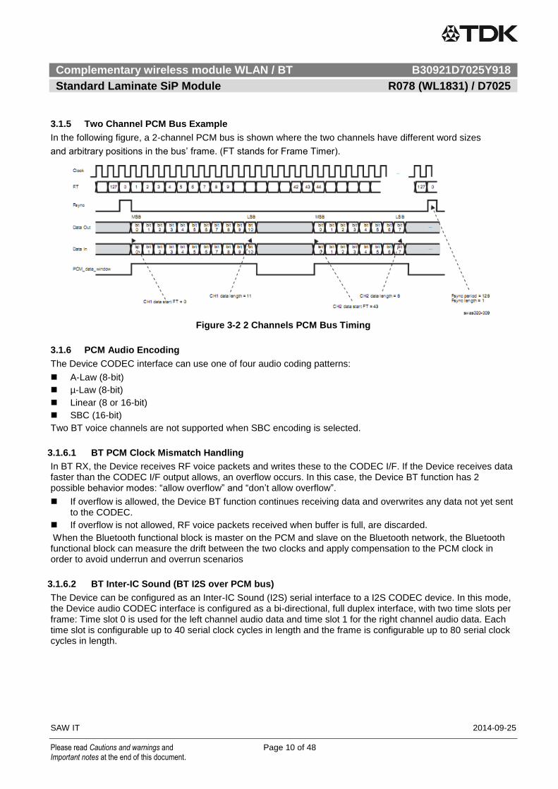
3.1.5 Two Channel PCM Bus Example
In the following figure, a 2-channel PCM bus is shown where the two channels have different word sizes
and arbitrary positions in the bus‟ frame. (FT stands for Frame Timer).
Figure 3-2 2 Channels PCM Bus Timing
3.1.6 PCM Audio Encoding
The Device CODEC interface can use one of four audio coding patterns:
A-Law (8-bit)
µ-Law (8-bit)
Linear (8 or 16-bit)
SBC (16-bit)
Two BT voice channels are not supported when SBC encoding is selected.
3.1.6.1 BT PCM Clock Mismatch Handling
In BT RX, the Device receives RF voice packets and writes these to the CODEC I/F. If the Device receives data faster than the CODEC I/F output allows, an overflow occurs. In this case, the Device BT function has 2 possible behavior modes: “allow overflow” and “don‟t allow overflow”.
If overflow is allowed, the Device BT function continues receiving data and overwrites any data not yet sent to the CODEC.
If overflow is not allowed, RF voice packets received when buffer is full, are discarded.
When the Bluetooth functional block is master on the PCM and slave on the Bluetooth network, the Bluetooth functional block can measure the drift between the two clocks and apply compensation to the PCM clock in order to avoid underrun and overrun scenarios
3.1.6.2 BT Inter-IC Sound (BT I2S over PCM bus)
The Device can be configured as an Inter-IC Sound (I2S) serial interface to a I2S CODEC device. In this mode, the Device audio CODEC interface is configured as a bi-directional, full duplex interface, with two time slots per frame: Time slot 0 is used for the left channel audio data and time slot 1 for the right channel audio data. Each time slot is configurable up to 40 serial clock cycles in length and the frame is configurable up to 80 serial clock cycles in length.

Complementary wireless module WLAN / BT B30921D7025Y918
Standard Laminate SiP Module R078 (WL1831) / D7025
SAW IT 2014-09-25
Please read Cautions and warnings and Page 11 of 48 Important notes at the end of this document.
3.2 Clocks and Power Management
3.2.1 Slow Clock / RTC clock
The slow clock is a free-running clock of 32.768 KHz which is supplied from an external clock source. It is connected to the RTC_CLK pin and is a digital square-wave signal in the range of 0-1.8V nom.
3.2.2 Fast Clock System
3.2.2.1 Fast clock using external crystal
The devices incorporate an internal crystal oscillator circuit for supporting a cost optimized crystal based fast clock scheme. Connection is as shown:
Figure 3-3 XTAL Connection
C1 = C2. Typically 8 - 22pF. Refer to Crystal manufacturer‟s recommendations.
R = 390K ohm (+/- 5% tolerance).
3.2.2.2 Fast Clock using external oscillator
CLK_IN_P is the main system fast clock and must meet the specifications as described in "Fast clock specifications" at the end of this document.
The clock must be one of the specified frequencies and the device incorporates an internal mechanism to detect this. The clock can be AC or DC coupled, sine or square wave.
Figure 3-4 Fast Clock Block Diagram

Complementary wireless module WLAN / BT B30921D7025Y918
Standard Laminate SiP Module R078 (WL1831) / D7025
SAW IT 2014-09-25
Please read Cautions and warnings and Page 12 of 48 Important notes at the end of this document.
3.2.3 Power Management
3.2.3.1 Block Diagram - internal DC2DC's
The Device incorporates three internal DC2DC's (switched-mode power supplies) to provide efficient internal and external supplies, derived from Vbat.
Figure 3-5 Internal DC2DC’s

Complementary wireless module WLAN / BT B30921D7025Y918
Standard Laminate SiP Module R078 (WL1831) / D7025
SAW IT 2014-09-25
Please read Cautions and warnings and Page 13 of 48 Important notes at the end of this document.
3.2.4 Reset / Power up system
After Vbat and VIO are fed to Device and while BT_EN, WLAN_EN are de-asserted (LOW), the device is in Shutdown state.
While in Shutdown state all functional blocks, internal DC2DC's and LDO's will be disabled. The power supplied to the functional blocks is cut off.
When one of the two signals BT_EN or WLAN_EN are asserted (High) a Power On Reset (POR) is performed.
Stable Slow Clock, VIO and Vbat are pre-requisites for successful POR.
3.2.4.1 Chip Top-level Power Up Sequence
Figure 3-6 Chip Top-level Power Up Sequence

Complementary wireless module WLAN / BT B30921D7025Y918
Standard Laminate SiP Module R078 (WL1831) / D7025
SAW IT 2014-09-25
Please read Cautions and warnings and Page 14 of 48 Important notes at the end of this document.
3.2.4.2 WLAN Power Up Sequence
Figure 3-7 WLAN Power Up Sequence
3.2.4.3 BT/BLE Power Up Sequence
Figure 3-8 BT Power Up Sequence

Complementary wireless module WLAN / BT B30921D7025Y918
Standard Laminate SiP Module R078 (WL1831) / D7025
SAW IT 2014-09-25
Please read Cautions and warnings and Page 15 of 48 Important notes at the end of this document.
3.3 WLAN Functional Block
3.3.1 WLAN MAC
R078 (WL1831) / D7025 MAC implements the IEEE standard 802.11 MAC sub-layer using both dedicated hardware and embedded firmware. The MAC hardware implements real-time functions, including access protocol management, encryption and decryption.
3.3.2 WLAN Baseband Processor
R078 (WL1831) / D7025 baseband processor implements the IEEE 802.11b/g/n PHY sub layers and has been optimized to perform well in conditions of high multipath and noise.
3.3.3 WLAN RF Radio
R078 (WL1831) / D7025 WLAN radio is a highly integrated radio processor designed for 802.11b/g/n applications, including internal front-end PA's.
3.3.4 Coexistence BT/BLE - WLAN
R078 (WL1831) / D7025 has been designed to support simultaneous operation of each of the major on-chip core functions. This operational coexistence is based on extensive frequency planning for each of the on-chip core functions, as well as a sophisticated MAC co-ordination scheme between Bluetooth and WLAN subsystems that allows operation in the same ISM frequency band.
3.3.5 WLAN RF Configuration and Power Options
The R078 (WL1831) / D7025 includes all RF switches, band pass filters and diplexer for complete WLAN (SISO) and BT RF system.
Figure 3-9 R078 (WL1831) / D7025 SISO configuration
3.3.5.1 SISO configuration (WL1831 device)
The diagram above shows WLAN and BT pins in standard SISO application.
Standard configuration for SISO:
WLAN 2.4GHz + BT
WLAN/BT 2.4GHz simultaneous RX/RX
Complementary wireless module WLAN / BT B30921D7025Y918
Standard Laminate SiP Module R078 (WL1831) / D7025
SAW IT 2014-09-25
Please read Cautions and warnings and Page 16 of 48 Important notes at the end of this document.
3.4 Bluetooth Functional Block
3.4.1 BT Digital Radio Processor (DRP)
The Device uses 8th-generation TI Bluetooth technology, with new features and improved radio performance.
3.4.2 BT Receiver
The receiver uses near-zero-IF architecture to convert the RF signal to baseband data. Received signal from the external antenna is input to an internal RF switch and a differential LNA (low-noise amplifier).
This signal is then passed to a mixer which down-converts the signal to an IF, followed by a filter and amplifier. The signal is then quantized by a sigma-delta ADC. The quantized signal is further processed to reduce the interference level.
The demodulator digitally down-converts the signal to zero IF and recovers the data stream by an adaptive decision mechanism. The demodulator includes EDR processing with state-of-the-art performance. It includes a maximum-likelihood sequence estimator (MLSE) for improved performance of basic-rate BR sensitivity, and adaptive equalization to enhance EDR modulation.
3.4.3 BT Transmitter
The transmitter is based on an all-digital sigma-delta PLL with a digitally controlled oscillator (DCO) as the RF frequency clock. The modulation is achieved by directly modulating the digital PLL. The power amplifier is also digitally controlled.
For EDR modulation, the transmitter uses a Polar-Modulation technique. In this mode, in addition to the frequency modulation that controls the direct-modulated ADPLL, an amplitude control modulates the PA, using the Digital-Transmitter block. This block receives the input bit-stream and converts these signals to phase-modulated control-words. The phase-modulated digital signal is then processed to provide frequency-modulation control to the ADPLL.
3.4.4 Class 1.5 Application
Device provides on-chip support for Class 2 and Class 1.5 applications. Class 1.5 is the normal operating mode after the initialization script has been sent to the Device.
It is called Class 1.5 as Device can transmit more than 4dBm on any BT modulation.
Refer to Bluetooth RF Performance specifications at end of document for more information.
3.4.5 Advanced Audio features
The Device includes Audio and Voice Processor (AVPR) targeted for off-loading the host CPU from coding voice/audio samples when running A2DP and WBS profiles.

Complementary wireless module WLAN / BT B30921D7025Y918
Standard Laminate SiP Module R078 (WL1831) / D7025
SAW IT 2014-09-25
Please read Cautions and warnings and Page 17 of 48 Important notes at the end of this document.
3.4.5.1 Assisted Wideband (WB) speech
Encode/Decode 16kHz PCM audio samples to/from 64kbps SBC frames
Fully compliant with the BT SIG Wideband speech profile
Figure 3-10 Device Wideband speech support
3.4.5.2 Assisted A2DP
Encode 44.1/48kHz PCM audio samples to Low/Mid/High Quality A2DP stream
Fully compliant with the BT SIG A2DP profile
Figure 3-11 Device Assisted A2DP

Complementary wireless module WLAN / BT B30921D7025Y918
Standard Laminate SiP Module R078 (WL1831) / D7025
SAW IT 2014-09-25
Please read Cautions and warnings and Page 18 of 48 Important notes at the end of this document.
3.5 Terminal Assignements
The view is from top side: A B C D E F G H J K L M N P
12 GND
BT_AUD_
FSYNC_S
B_DATA
GND VIO GND GND GND GND NU NU NU NU GND GND 12 DIGITAL
11 GND
BT_AUD_I
N_SB_CL
K
GND GND GNDSDIO_D2_
WL
SDIO_CLK
_WLGND
BT_AUD_
OUTGND NU GND GND NU 11 RF
10 GNDBT_AUD_
CLKGND
FUNC2_B
TGND
SDIO_D3_
WL
SDIO_D0_
WLGND
DC2DC_R
EQ_MODE
_SOC
CLK_REQ
_OUTGND GND GND GND 10 Power
9 GND GND GNDFUNC1_B
TGND
SDIO_CM
D_WL
SDIO_D1_
WLGND
SLOW_CL
KNU NU GND GND NU 9 GND
8 NU GNDJTAG_TC
K
JTAG_TD
OGND GND GND
COEX_M
WS_BT_W
L_TX_O
COEX_M
WS_FRAM
E_SYNC
NU NU GND GND NU 8 CLOCK
7 GND GNDJTAG_TM
SGND GND
COEX_M
WS_ACTI
VE
RX_SW_F
EM_WL
COEX_M
WS_RX_P
RI
NU NU GND GND GND NU 7
DIGITAL
High
Speed
6 NU GNDPBIAS_TE
STP_WGND GND
DC2DC_R
EQ_OUT_
SOC
WLAN_IR
Q
UART_DE
BUGGPIO_2 NU NU GND GND NU 6 Not Used
5 GND GNDPDET_TE
STM_WGND GND GND
WLAN_EN
_SOC
FEM_PA_
EN_WLNU GPIO_1 GND GND GND GND 5
4 GND GND JTAG_TDI GNDBT_EN_S
OC
BT_HCI_R
X
BT_HCI_T
X
BT_HCI_R
TS
BT_HCI_C
TSGPIO_3 GND VBAT1 VBAT2 VBAT3 4
311bg_ANT
_1GND GND GND GND GND GND GND GND GND GND GND GND GND 3
2 GND GND GND GND GND CLK_IN_P CLK_IN_M GND GND GND GND GND GND GND 2
1 GND GND GND GND GND GND GND GNDPA_DC2D
C_IN
PA_DC2D
C_OUTGND GND GND GND 1
A B C D E F G H J K L M N P
Top view
Figure 3-12 Terminal Assignements

Complementary wireless module WLAN / BT B30921D7025Y918
Standard Laminate SiP Module R078 (WL1831) / D7025
SAW IT 2014-09-25
Please read Cautions and warnings and Page 19 of 48 Important notes at the end of this document.
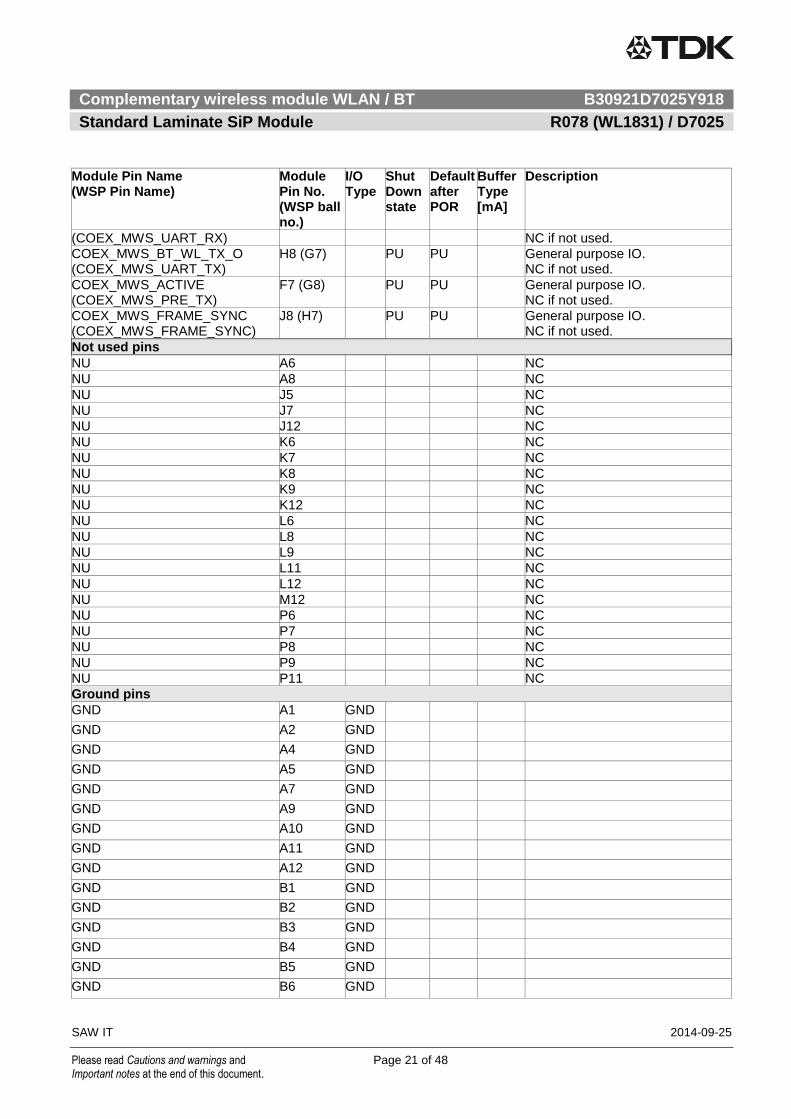
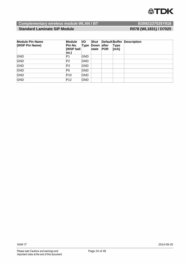
3.6 Terminal Functions
Pin names and pin numbers in bracket apply to WSP pin out.
Table 3-3 Terminal Functions
Module Pin Name (WSP Pin Name)
Module Pin No. (WSP ball no.)
I/O Type
Shut Down state
Default after POR
Buffer Type [mA]
Description
WLAN pins: I/O signals
SDIO_CLK_WL (SDIO_CLK_WL) G11 (E11) IN HiZ HiZ WLAN SDIO clock. Must be driven by the host.
SDIO_CMD_WL(SDIO_CMD_WL) F9 (D8) IN HiZ HiZ WLAN SDIO command in. Host must pull up.
SDIO_D0_WL (SDIO_D0_WL) G10 (E10) I/O HiZ HiZ WLAN SDIO data bit 0. Host must pull up.
SDIO_D1_WL (SDIO_D1_WL) G9 (E9) I/O HiZ HiZ WLAN SDIO data bit 1. Host must pull up.
SDIO_D2_WL (SDIO_D2_WL) F11 (D11) I/O HiZ HiZ WLAN SDIO data bit 2. Host must pull up.
SDIO_D3_WL (SDIO_D3_WL) F10 (D10) I/O HiZ PU WLAN SDIO data bit 3. Changes state to PU at WL_EN or BT_EN assertion for card detect. Later disabled by the SW during init. Host must pull up.
WLAN_IRQ (IRQ_WL) G6 (E3)
OUT PD Drive 0 SDIO available, interrupt out. Active high. To use WL_RS232_TX/RX lines, need to pull up with 10K resistor.
GPIO_1 (GPIO1) K5 (H1) I/O PD PD Option: WL_RS232_TX (when IRQ_WL = 1 at power up)
GPIO_2 (GPIO2) J6 (H2) I/O PD PD Option: WL_RS232_RX (when IRQ_WL = 1 at power up)
GPIO_3 (UART_DBG_WL) K4 (G4) OUT PU PU WLAN logger Option: GPIO3
FEM_PA_EN_WL (GPIO13)
H5 (F2)
NC
RX_SW_FEM_WL (SW_CTRL_BG_IO1)
G7 (F3) NC
PBIAS_TESTP_W (PABIAS_OUT_FEM_TESTP_WL)
C6 (C7) ANA NC
PDET_TESTM_W (PDET_IN_FEM_TESTM_WL)
C5 (C6) ANA NC
WLAN Pins: RF antenna
11bg_ANT_1 A3 RF WLAN BG / BT RX and TX 50Ω input and output. No external matching required.
BT pins: I/O Signals
BT_HCI_RX (HCI_RX_BT) F4 (E7) IN PU PU HCI UART RX from host. Shared HCI I/F for BT. NC if not used.
BT_HCI_TX (HCI_TX_BT) G4 (F7) OUT PU PU HCI UART TX to host. Shared HCI I/F.NC if not used.
BT_HCI_RTS (HCI_RTS_BT)
H4 (G6) OUT PU PU HCI UART RTS to host. Shared HCI I/F. NC if not used.

Complementary wireless module WLAN / BT B30921D7025Y918
Standard Laminate SiP Module R078 (WL1831) / D7025
SAW IT 2014-09-25
Please read Cautions and warnings and Page 20 of 48 Important notes at the end of this document.
Module Pin Name (WSP Pin Name)
Module Pin No. (WSP ball no.)
I/O Type
Shut Down state
Default after POR
Buffer Type [mA]
Description
BT_HCI_CTS (HCI_CTS_BT) J4 (F6) IN PU PU HCI UART CTS from host. Shared HCI I/F. NC if not used.
UART_DEBUG (UART_DEBUG_BT)
H6 (G2) OUT PU PU BT UART debug (logger). NC if not used.
FUNC1_BT (FUNC1_BT) D9 (E8) OUT PD PD Optional: BT_HOST_WAKE_UP signal to wake-up the HOST from BT. NC if not used.
FUNC2_BT (FUNC2_BT) D10 (B11) IN PD PD Optional: BT_WAKE_UP Bluetooth wakeup from HOST. NC if not used.
BT_AUD_CLK (AUD_CLK_BT) B10 (G11) OUT PD PD BT PCM/I2S bus clock. NC if not used.
BT_AUD_FSYNC_SB_DATA (AUD_FSYNC_BT)
B12 (H11) OUT PD PD BT PCM/I2S bus frame sync. NC if not used.
BT_AUD_IN_SB_CLK (AUD_IN_BT)
B11 (G9) IN PD PD BT PCM/I2S bus data input. NC if not used.
BT_AUD_OUT (AUD_OUT_BT) J11 (G10) OUT PD PD BT PCM/I2S bus data output. NC if not used.
JTAG pins
JTAG_TCK C8 (F11) IN PD PD JTAG_TCK NC if not used
JTAG_TMS C7 (F8) IN PD PD JTAG_TMS NC if not used
JTAG_TDI C4 (F9) IN PD PD JTAG_TDI NC if not used
JTAG_TDO D8 (F10) OUT PD PD JTAG_TDO NC if not used
Clock pins
CLK_IN_P F2 (E4) ANA FREF/TCXO input for all functional blocks
CLK_IN_M G2 (E5) ANA Connect to GND
SLOW_CLK (RTC_CLK) J9 (H8) ANA Sleep clock 32.768 kHz
CLK_REQ_OUT K10 (K11) OUT PD PD Request external fast clock NC if not used.
Enable pins
BT_EN_SOC (BT_EN) E4 (E2) IN PD PD High = enable
WLAN_EN_SOC (WLAN_EN) G5 (E1) IN PD PD High = enable Power management pins
VBAT1 M4 POW Battery voltage
VBAT2 N4 POW Battery voltage
VBAT3 P4 POW Battery voltage
VIO D12 POW 1.8V I/O power supply
PA_DC2DC_IN J1 POW PA power supply input, with internal PA_DC2DC connect to pin PA_DC2DC_OUT K1.
PA_DC2DC_OUT K1 POW DC2DC output for PA supply, with internal PA_DC2DC connect to pin PA_DC2DC_IN J1.
DC2DC_REQ_OUT_SOC (NU) F6 (D3) NC
DC2DC_REQ_MODE_SOC (NU) J10 (J10) NC
Co-existence signals
COEX_MWS_RX_PRI H7 (G5) PU PU General purpose IO.
Complementary wireless module WLAN / BT B30921D7025Y918
Standard Laminate SiP Module R078 (WL1831) / D7025
SAW IT 2014-09-25
Please read Cautions and warnings and Page 21 of 48 Important notes at the end of this document.
Module Pin Name (WSP Pin Name)
Module Pin No. (WSP ball no.)
I/O Type
Shut Down state
Default after POR
Buffer Type [mA]
Description
(COEX_MWS_UART_RX) NC if not used.
COEX_MWS_BT_WL_TX_O (COEX_MWS_UART_TX)
H8 (G7) PU PU General purpose IO. NC if not used.
COEX_MWS_ACTIVE (COEX_MWS_PRE_TX)
F7 (G8) PU PU General purpose IO. NC if not used.
COEX_MWS_FRAME_SYNC (COEX_MWS_FRAME_SYNC)
J8 (H7) PU PU General purpose IO. NC if not used.
Not used pins
NU A6 NC
NU A8 NC
NU J5 NC
NU J7 NC
NU J12 NC
NU K6 NC
NU K7 NC
NU K8 NC
NU K9 NC
NU K12 NC
NU L6 NC
NU L8 NC
NU L9 NC
NU L11 NC
NU L12 NC
NU M12 NC
NU P6 NC
NU P7 NC
NU P8 NC
NU P9 NC
NU P11 NC
Ground pins
GND A1 GND
GND A2 GND
GND A4 GND
GND A5 GND
GND A7 GND
GND A9 GND
GND A10 GND
GND A11 GND
GND A12 GND
GND B1 GND
GND B2 GND
GND B3 GND
GND B4 GND
GND B5 GND
GND B6 GND

Complementary wireless module WLAN / BT B30921D7025Y918
Standard Laminate SiP Module R078 (WL1831) / D7025
SAW IT 2014-09-25
Please read Cautions and warnings and Page 22 of 48 Important notes at the end of this document.
Module Pin Name (WSP Pin Name)
Module Pin No. (WSP ball no.)
I/O Type
Shut Down state
Default after POR
Buffer Type [mA]
Description
GND B7 GND
GND B8 GND
GND B9 GND
GND C1 GND
GND C2 GND
GND C3 GND
GND C9 GND
GND C10 GND
GND C11 GND
GND C12 GND
GND D1 GND
GND D2 GND
GND D3 GND
GND D4 GND
GND D5 GND
GND D6 GND
GND D7 GND
GND D11 GND
GND E1 GND
GND E2 GND
GND E3 GND
GND E5 GND
GND E6 GND
GND E7 GND
GND E8 GND
GND E9 GND
GND E10 GND
GND E11 GND
GND E12 GND
GND F1 GND
GND F3 GND
GND F5 GND
GND F8 GND
GND F12 GND
GND G1 GND
GND G3 GND
GND G8 GND
GND G12 GND
GND H1 GND

Complementary wireless module WLAN / BT B30921D7025Y918
Standard Laminate SiP Module R078 (WL1831) / D7025
SAW IT 2014-09-25
Please read Cautions and warnings and Page 23 of 48 Important notes at the end of this document.
Module Pin Name (WSP Pin Name)
Module Pin No. (WSP ball no.)
I/O Type
Shut Down state
Default after POR
Buffer Type [mA]
Description
GND H2 GND
GND H3 GND
GND H9 GND
GND H10 GND
GND H11 GND
GND H12 GND
GND J2 GND
GND J3 GND
GND K2 GND
GND K3 GND
GND K11 GND
GND L1 GND
GND L2 GND
GND L3 GND
GND L4 GND
GND L5 GND
GND L7 GND
GND L10 GND
GND M1 GND
GND M2 GND
GND M3 GND
GND M5 GND
GND M6 GND
GND M7 GND
GND M8 GND
GND M9 GND
GND M10 GND
GND M11 GND
GND N1 GND
GND N2 GND
GND N3 GND
GND N5 GND
GND N6 GND
GND N7 GND
GND N8 GND
GND N9 GND
GND N10 GND
GND N11 GND
GND N12 GND
Complementary wireless module WLAN / BT B30921D7025Y918
Standard Laminate SiP Module R078 (WL1831) / D7025
SAW IT 2014-09-25
Please read Cautions and warnings and Page 24 of 48 Important notes at the end of this document.
Module Pin Name (WSP Pin Name)
Module Pin No. (WSP ball no.)
I/O Type
Shut Down state
Default after POR
Buffer Type [mA]
Description
GND P1 GND
GND P2 GND
GND P3 GND
GND P5 GND
GND P10 GND
GND P12 GND

Complementary wireless module WLAN / BT B30921D7025Y918
Standard Laminate SiP Module R078 (WL1831) / D7025
SAW IT 2014-09-25
Please read Cautions and warnings and Page 25 of 48 Important notes at the end of this document.
4 Design Goal Specifications
Section Disclaimer
This Specification is based upon the Texas Instruments WL183x Data Sheet version 1.4, and is subject to any subsequent changes in applicable Texas Instruments documentation and software.
Any parameter marked TBD indicates that this is yet to be determined by TDK design/testing. Any parameter marked TBC indicates that this is yet to be determined in an update of Texas Instruments documentation.
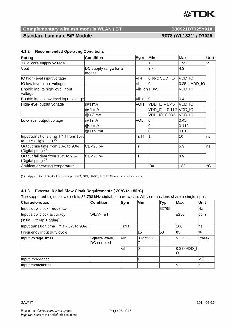
4.1 General Chip Requirements and Operation
All parameters are measured as follows unless stated otherwise: VlO=1.8V
4.1.1 Absolute Maximum Ratings (1)
Value Unit
VBAT(2)
-0.5 to 5.5(4)
V
VIO -0.5 to 2.1 V
Input voltage to Analog pins (3)
-0.5 to 2.1 V
Input voltage to all other pins -0.5 to (VDD_IO + 0.5V)
V
Operating ambient temperature range -30 to +85(5)
°C
ESD Stress Voltage (6)
Human Body Model (7)
RF pins >500 V
Other >1000 V
Charged Device Model (8)
RF pins >300 V
Other >250 V
(1) Stresses beyond those listed under “absolute maximum ratings” may cause permanent damage to the device. These are stress ratings only and functional operation of the device at these or any other conditions beyond those indicated under “recommended operating conditions” is not implied. Exposure to absolute-maximum-rated conditions for extended periods may affect device reliability.
(2) The following signals are from the VBAT group: VBAT1, VBAT2, VBAT3
(3) Analog pins: 11bg_ANT_1.
(4) 5.5V up to 10s cumulative in 7 years. 5V cumulative to 250s, 4.8V cumulative to 2.33 years – all includes charging dips and peaks.
(5) Operating free-air temperature range. The device can be reliably operated for 7 years at Tambient of 85˚C, assuming 25% active mode and 75% sleep mode (15,400 cumulative active power-on hours).
(6) Electrostatic discharge (ESD) to measure device sensitivity/immunity to damage caused by electrostatic discharges into the device.
(7) Level listed is the passing level per ANSI/ESDA/JEDEC JS-001. JEDEC document JEP155 states that 500V HBM allows safe manufacturing with a standard ESD control process, and manufacturing with less than 500V HBM is possible if necessary precautions are taken. Pins listed as 1000V may actually have higher performance.
(8) Level listed is the passing level per EIA-JEDEC JESD22-C101E. JEDEC document JEP157 states that 250 V CDM allows safe manufacturing with a standard ESD control process, and manufacturing with less than 250V CDM is possible if necessary precautions are taken. Pins listed as 250 V may actually have higher performance.
Complementary wireless module WLAN / BT B30921D7025Y918
Standard Laminate SiP Module R078 (WL1831) / D7025
SAW IT 2014-09-25
Please read Cautions and warnings and Page 26 of 48 Important notes at the end of this document.
4.1.2 Recommended Operating Conditions
Rating Condition Sym Min Max Unit
1.8V core supply voltage 1.7 1.95 V
Vbat DC supply range for all modes
3.4 4.3
IO high-level input voltage VIH 0.65 x VDD_IO VDD_IO
IO low-level input voltage VIL 0 0.35 x VDD_IO
Enable inputs high-level input voltage
Vih_en 1.365 VDD_IO
Enable inputs low-level input voltage Vil_en 0 0.4
High-level output voltage @4 mA VOH VDD_lO – 0.45 VDD_IO
@ 1 mA VDD_lO – 0.112 VDD_IO
@0.3 mA VDD_IO- 0.033 VDD_IO
Low-level output voltage @4 mA VOL 0 0.45
@ 1 mA 0 0.112
@0.09 mA 0 0.01
Input transitions time Tr/Tf from 10% to 90% (Digital IO)
(1)
Tr/Tf 1 10 ns
Output rise time from 10% to 90% (Digital pins)
(1)
CL <25 pF Tr 5.3 ns
Output fall time from 10% to 90% (Digital pins)
(1)
CL <25 pF Tf 4.9
Ambient operating temperature -30 +85 °C
(1) Applies to all Digital lines except SDIO, SPI, UART, I2C, PCM and slow clock lines
4.1.3 External Digital Slow Clock Requirements (-30°C to +85°C)
The supported digital slow clock is 32.768 kHz digital (square wave). All core functions share a single input.
Characteristics Condition Sym Min Typ Max Unit
Input slow clock frequency 32768 Hz
Input slow clock accuracy
(initial + temp + aging)
WLAN, BT ±250 ppm
Input transition time Tr/Tf -lO% to 90% Tr/Tf 100 ns
Frequency input duty cycle 15 50 85 %
Input voltage limits Square wave, DC-coupled
Vih 0.65xVDD_IO
VDD_IO Vpeak
Vil 0 0.35xVDD_IO
Input impedance 1 MΩ
Input capacitance 5 pF

Complementary wireless module WLAN / BT B30921D7025Y918
Standard Laminate SiP Module R078 (WL1831) / D7025
SAW IT 2014-09-25
Please read Cautions and warnings and Page 27 of 48 Important notes at the end of this document.
4.1.4 External fast clock Crystal Requirements and operation (-30°C to +85°C)
Characteristics Condition Min Typ Max Unit
Supported frequencies 26, 38.4 MHz
Frequency accuracy Initial + temp + aging ±20 ppm
Load capacitance, CL(1)
5 13 pF
Equivalent Series Resistance, ESR 60 ohms
Drive level 100 uW
1) Load capacitance, CL = [C1.C2] / [C1 + C2] + CP, where C1, C2 are the capacitors connected on CLK_IN_P & CLK_IN_M respectively and CP is the parasitic capacitance (typically 1-2pF).
For example, for C1 = C2 = 12pF and CP = 2pF, then CL = 8pF.
4.1.5 External TCXO CLK Requirements (-30°C to +85°C)
Parameter Conditions Min Typ Max Unit
Supported frequency 26, 38.4 MHz
Frequency accuracy Total short and long term ±20 ppm
Input voltage limits (TCXO_P) Sine wave/
ac-coupled
2.4GHz WLAN 0.2 1.4 Vp-p
Input impedance, 26 MHz
RP Input resistance 20 kΩ
CP Input capacitance 2.5 pF
Input impedance, 38.4 MHz
RP Input resistance 15 kΩ
CP Input capacitance 2.5 pF
Power-up time (1)
5 ms
Phase noise 2.4GHz for 38.4MHz
20MHz SISO (2)
Measured at 1 KHz offset -120 dBc/Hz
Measured at 10 KHz offset -130 dBc/Hz
Measured at 100 KHz offset -135 dBc/Hz
Phase noise 2.4GHz for 38.4MHz
40MHz SISO (2)
Measured at 1 KHz offset -125 dBc/Hz
Measured at 10 KHz offset -132 dBc/Hz
Measured at 100KHZ offset -136.5 dBc/Hz
(1) Power-up time is calculated from the time CLK_REQ_OUT asserted till the time the TCXO_CLK amplitude is within voltage limit
specified above and TCXO_CLK frequency is within 0.1 ppm of final steady state frequency.
(2) The phase noise numbers listed here must be met at 38.4 MHz. For other frequencies the phase noise requirement is corrected by adding 20 x log10(fTCXO / 38.4e6) dB. Specifically, for 26 MHz TCXO, the correction factor would be -3.4 dB.
* The slope of the clock at zero-crossings should not be less than that of a 200 mVp-p sine-wave . i.e. 26MHz clock: 16V/μs (for 11bg band) 38.4MHz clock: 24V/μs (for 11bg band)

Complementary wireless module WLAN / BT B30921D7025Y918
Standard Laminate SiP Module R078 (WL1831) / D7025
SAW IT 2014-09-25
Please read Cautions and warnings and Page 28 of 48 Important notes at the end of this document.
4.2 WLAN RF Performance
All specifications in this draft data sheet are design goal level and subject to change. All specifications have been measured using TDK CB (Carrier Board) and are given at the module pins (Carrier Board insertion loss is de-embedded). All measurements have been performed over VBAT voltage range from 3.4V to 4.3V and over temperature range from -30°C to +85°C.
* 11n 40MHz bandwidth function is available. However the RF performance is guaranteed by only WL183x.
4.2.1 WLAN 2.4 GHz Radio Characteristics
4.2.1.1 WLAN 2.4 GHz Receiver RF Characteristics
Characteristics Condition Min Typ Max Unit
Operation frequency range 2400 2480 MHz
Sensitivity (ANT1) 20MHz bandwidth. At < 10% PER limit
1 Mbps DSSS -91 dBm
54 Mbps OFDM -70
MCS7 -65
Max Input Level At < 10% PER limit
OFDM (11g/n) –19 dBm
CCK –4
Adjacent Channel Rejection at sensitivity level +3 for OFDM and +6 for CCK
2Mbps 42.7 dB
11 Mbps 37.9
54 Mbps 2 LO leakage –80 dBm
4.2.1.2 WLAN 2.4 GHz Receiver Blocking Characteristics Per Band
The R078 (WL1831) / D7025 is designed to coexist with co-located cellular transmitters. Table below lists typical cellular interference sources and the corresponding maximum power from the cellular interference source that can be present at the input terminal of R078 (WL1831) / D7025, such that WLAN receiver sensitivity is not degraded by more than 1 dB. (Further improvement is achieved by antenna isolation)
Characteristics Condition Min Typ Max Unit
Blocking performance at other bands 776 to 794 MHz (CDMA) +10 dBm
824 to 849 MHz (GMSK) +10
824 to 849 MHz (EDGE) +10
824 to 849 MHz (CDMA) +10
880 to 915 MHz (GMSK) +21
880 to 915 MHz (EDGE) +21
1710 to 1785 MHz (GMSK) +3
1710 to 1785 MHz (EDGE) +3
1850 to 1910 MHz (GMSK) -3
1850 to 1910 MHz (EDGE) -3
1850 to 1910 MHz (CDMA) -10
1850 to 1910 MHz (WCDMA) -10
1920 to 1980 MHz (WCDMA) -10

Complementary wireless module WLAN / BT B30921D7025Y918
Standard Laminate SiP Module R078 (WL1831) / D7025
SAW IT 2014-09-25
Please read Cautions and warnings and Page 29 of 48 Important notes at the end of this document.
4.2.1.3 WLAN 2.4 GHz Transmitter power
RF transmission (Tx) tests are done in continuous transmission.
Characteristics Condition 11bg_ANT_1 pin WLAN_BG2 pin Unit
Min Typ Max Min Typ Max
Maximum output power
1 Mbps +12 +15 dBm
11Mbps +12 +15
6 Mbps at EVM: -10 dB, +10 +13 +16 +19
54 Mbps at EVM: -25 dB +9 +12 +13.5 +15
MCS0 (Greenfield) at EVM: -10 dB
+9 +13 +15.6 +19
MCS7 (Greenfield) at EVM: -28 dB
+8 +11 +12.1
+14
Output power accuracy ±1.5 ±1.5 dB
Transmit power control resolution
0.125 0.125 dB
4.2.1.4 WLAN 2.4 GHz Transmitter out-of-band emissions
Table below shows 2.4GHz WLAN transmitter out-of-band emissions for each band listed in the Condition column. The wideband noise at 2.4GHz WLAN antenna port is also listed.
Characteristics Condition Min Typ Max Unit
Cellular bands out-of-band broadband emissions(1)
746 to 764 MHz (CDMA1) -145 dBm/Hz
869 to 894 MHz (GSM850) -145
925 to 960 MHz (EGSM900) -138
1570 to 1580 MHz (GPS) -142
1596 to 1609 MHz (GLONASS) -130
1805 to 1880 MHz (DCS1800) -140
1930 to 1990 MHz (PCS1900) -120
2110 to 2170 MHz -129
Cellular bands out-of-band spurious emissions
746 to 764 MHz (CDMA) -44.2(4)
dBm 869 to 894 MHz (CDMA, GSM850) -44.2
(4)
925 to 960 MHz (EGSM900) -44.2(4)
1570 to 1580 MHz (GPS) -44.2(4)
1805 to 1880 MHz (DCS1800) -44.2
(4)
1930 to 1990 MHz (PCS1900, CDMA) -44.2(4)
2110 to 2170 MHz -44.2(4)
Spurious emission during operation at 1MHz RBW
30MHz – 1GHz –55(2)
dBm
2nd
harmonic –33(3)
3rd
harmonic –33(3)
4th harmonic –33
(3)
5th harmonic –33
(3)
(1) Figures are for max transmission power for all available modulations. The setup noise floor is -167dBm/Hz.
(2) Based on TI IC performance
(3) ETSI limit plus 3dB margin
(4) FCC conductive limit plus 3dB margin

Complementary wireless module WLAN / BT B30921D7025Y918
Standard Laminate SiP Module R078 (WL1831) / D7025
SAW IT 2014-09-25
Please read Cautions and warnings and Page 30 of 48 Important notes at the end of this document.
4.2.1.5 2.4GHz WLAN Current Consumption
Active Current
Spec item (1)
MIN TYP
MAX
Units
Tx 11CCK @15dBm 345 380 mA
Tx 54OFDM @12dBm 290 320 mA
Rx 65 75 mA (1) All measured at ANT1 and the 3.6V VBAT rail of the solution. TCXO current included.
4.3 Bluetooth RF Performance
All specifications in this draft data sheet are design goal level and subject to change. All specifications have been measured using TDK CB (Carrier Board) and are given at the module pins (Carrier Board insertion loss is de-embedded). All measurements have been performed over VBAT voltage range from 3.4V to 4.3V and over temperature range from -30°C to +85°C.
4.3.1 Bluetooth BR, EDR Receiver Characteristics—In-Band Signals
Characteristics Condition Min Typ Max Bluetooth Spec
Unit
Operation frequency range
2402 2480 MHz
Channel spacing 1 MHz
Input impedance 50 Ω Sensitivity (1)
Dirty TX on BR, BER = 0.1% –86 –90 –70 dBm
EDR2, BER = 0.01% –85 –89 –70
EDR3, BER = 0.01% –78 –82 –70
EDR BER floor at sensitivity + 10 dB, dirty TX off (for 1,600,00 bits)
EDR2, BER = 0.1% 1e-6 1e-5
EDR3, BER = 0.1% 1e-6 1e-5
Maximum useable input power
BR, BER = 0.1% –5 –20 dBm
EDR2, BER = 0.1% –10 –20 EDR3, BER = 0.1% –10 –20
Intermodulation characteristics
Level of interferers For n = 3, 4, and 5
–36 –30 –39 dBm
C/I performance Note: Numbers show wanted-signal to interfering-signal ratio. Smaller numbers indicate better C/I performance. Image = –1 MHz
BR, co-channel 8 10 11 dB
EDR, co-channel EDR2 9.5 12 13
EDR3 16.5 20 21
BR, adjacent ±1 MHz –10 –3 0
EDR, adjacent
±1MHz, (image)
EDR2 –10 –3 0
EDR3 –5 2 5
BR, adjacent +2 MHz –38 –33 –30 EDR, adjacent +2MHz
EDR2 –38 –33 –30
EDR3 –38 –28 –25
BR, adjacent –2 MHz –28 –22 –20
EDR, adjacent –2MHz,
EDR2 –28 –20 –20
EDR3 –22 –13 –13
BR, adjacent | ±3 | MHz –45 –42 –40
EDR, adjacent
| ±3 | MHz
EDR2 –45 –42 –40
EDR3 –44 –36 –33
RF return loss –10 dB (1) Sensitivity degradation up to –3 dBm may occur due to fast clock harmonics with dirty Tx on.

Complementary wireless module WLAN / BT B30921D7025Y918
Standard Laminate SiP Module R078 (WL1831) / D7025
SAW IT 2014-09-25
Please read Cautions and warnings and Page 31 of 48 Important notes at the end of this document.
4.3.2 Bluetooth Receiver Characteristics—General Blocking
Characteristics Condition Min Typ Bluetooth Spec Unit
Blocking performance over full range, according to Bluetooth specification (1)
30 to 2000 MHz -6 -10 dBm
2000 to 2399 MHz -6 -27
2484 to 3000 MHz -6 -27
3 to 12.75 GHz -6 -10 (1) Exceptions taken out of the total 24 allowed in the Bluetooth spec.
4.3.3 Bluetooth Receiver Characteristics—GFSK, EDR2, EDR3 Blocking Per Band
Characteristics Condition Min Typ Unit
Blocking performance for various cellular bands. Hopping on. Wanted signal: -3 dB from sensitivity, with modulated continuous blocking signal. BER = 0.1% for BT BR, BER = 0.01% for BT EDR, PER = 1%
776 to 794 MHz (CDMA) (1) +13 dBm
824 to 849 MHz (GMSK) (1) +22
824 to 849 MHz (EDGE) (1) +14
824 to 849 MHz (CDMA,QPSK) (1) +13
880 to 915 MHz (GMSK) +11
880 to 915 MHz (EDGE) +10
1710 to 1875 MHz (GMSK) +17
1710 to 1875 MHz (EDGE) +3
1850 to 1910 MHz (GMSK) -3
1850 to 1910 MHz (EDGE) -5
1850 to 1910 MHz (CDMA,QPSK) -5
1850 to 1910 MHz (WCDMA,QPSK) -1
1920 to 1980 MHz (WCDMA,QPSK) -2
(1) Expect for frequencies where (3 x F_BLOCKER falls within the BT band (2400-2483.5 MHz).
4.3.4 Bluetooth Transmitter, BR, Class 1.5
Characteristics Min Typ Max Bluetooth Spec
Unit
RF output power 9 11 dBm
Gain control range 30 dB
Power control step 2 5 8 2 to 8
Adjacent channel power |M–N| = 2 –43 –35 < –20 dBm
Adjacent channel power |M–N| > 2 –48 –40 < –40
4.3.5 Bluetooth Transmitter, EDR, Class 1.5
Characteristics Min Typ Max Bluetooth Spec
Units
EDR relative power –2 1 –4 to +1 dB Gain control range 30
Power control step 2 5 8 2 to 8
Adjacent channel power |M–N| = 1 –36 –30 <–26 dBm
Adjacent channel power |M–N| = 2 –30 –23 <–20
Adjacent channel power |M–N| > 2 –42 –40 <–40

Complementary wireless module WLAN / BT B30921D7025Y918
Standard Laminate SiP Module R078 (WL1831) / D7025
SAW IT 2014-09-25
Please read Cautions and warnings and Page 32 of 48 Important notes at the end of this document.
4.3.6 Bluetooth Modulation, BR—Class 1.5
Characteristics Condition Sym Min Typ Max Bluetooth Spec
Unit
–20 dB BW 925 995 1000 kHz
Average deviation detector bandwidth –10 MHz
Mod Data = 4-1, 4-0 1111000011110000...
dF1 avg 145 160 170 140 to 175 kHz
Instantaneous deviation
Mod data = 10101… 1010101...
dF2 max 120 130 > 115 kHz
dF2/dF1 85 88 > 80 %
Carrier frequency drift DH1 -25 25 < ±25 kHz
DH3 and DH5 -35 35 < ±40
Drift rate lfk+5 – fkl , k = 0 …. max
15 < 20 kHz/ 50µs s Initial carrier
frequency tolerance F0 –fTX -25 25 <± 75 kHz
4.3.7 Bluetooth Modulation, EDR, Class 1.5
Characteristics Condition Min Typ Max Bluetooth spec
Unit
Carrier frequency stability -5 5 ≤10 kHz
Initial carrier frequency tolerance
-25 25 ± 75 kHz
RMS DEVM (1) EDR2 4 15 20 %
EDR3 4 10 13 %
99% DEVM (1) EDR2 30 30 %
EDR3 20 20 %
Peak DEVM (1) EDR2 9 25 35 %
EDR3 9 18 25 %
4.3.8 Bluetooth Transceiver, Out-of-Band Emissions
Characteristics Condition Typ Max Unit
TX out-of-band emissions 746 to 764 MHz (CDMA) -143 dBm/Hz
869 to 894 MHz (CDMA1, GSM) -141
925 to 960 MHz (E-GSM) -140
1570 to 1580 MHz (GPS) -137
1598 to 1607 MHz (GLONASS) -137
1805 to 1880 MHz (DCS, WCDMA)
-133
1930 to 1990 MHz (PCS) -131
2110 to 2170 MHz (WCDMA) -121
Complementary wireless module WLAN / BT B30921D7025Y918
Standard Laminate SiP Module R078 (WL1831) / D7025
SAW IT 2014-09-25
Please read Cautions and warnings and Page 33 of 48 Important notes at the end of this document.
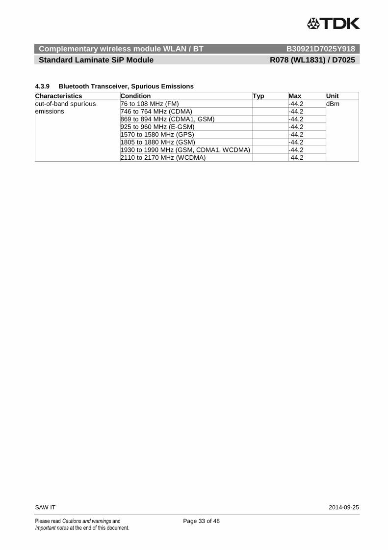
4.3.9 Bluetooth Transceiver, Spurious Emissions
Characteristics Condition Typ Max Unit
out-of-band spurious emissions
76 to 108 MHz (FM) -44.2 dBm
746 to 764 MHz (CDMA) -44.2
869 to 894 MHz (CDMA1, GSM) -44.2
925 to 960 MHz (E-GSM) -44.2
1570 to 1580 MHz (GPS) -44.2
1805 to 1880 MHz (GSM) -44.2
1930 to 1990 MHz (GSM, CDMA1, WCDMA) -44.2
2110 to 2170 MHz (WCDMA) -44.2

Complementary wireless module WLAN / BT B30921D7025Y918
Standard Laminate SiP Module R078 (WL1831) / D7025
SAW IT 2014-09-25
Please read Cautions and warnings and Page 34 of 48 Important notes at the end of this document.
4.4 BLE RF performance
All specifications in this draft data sheet are design goal level and subject to change. All specifications have been measured using TDK CB (Carrier Board) and are given at the module pins (Carrier Board insertion loss is de-embedded). All measurements have been performed over VBAT voltage range from 3.4V to 4.3V and over temperature range from -30°C to +85°C.
* BLE function is available. However the RF performance is guaranteed by only WL183x.
4.4.1 BLE Receiver Characteristics—In-Band Signals
Characteristics Condition (2)
Min Typ Max BLE
Spec Unit
Operation frequency range
2402 2480 MHz
Channel spacing 2 MHz
Input impedance 50 Ω
Sensitivity (1)
Dirty TX on dirty Tx on -88 –91 ≤ -70 dBm
Maximum useable input power
-5 ≥ -10 dBm
Intermodulation characteristics
Level of interferers For n = 3, 4, and 5
-36 -30 ≥ -50 dBm
C/I performance Note: Numbers show wanted-signal to interfering-signal ratio. Smaller numbers indicate better C/I performance. Image = –1 MHz
BLE, co-channel 8 12 ≤ 21 dB
BLE, adjacent ±1 MHz –5 0 ≥ 15
BLE, adjacent +2 MHz –45 –38 ≤ -17
BLE, adjacent –2 MHz –22 –15 ≤ -15
BLE, adjacent ≥|±3| MHz –47 –40 ≤ -27
(1) Sensitivity degradation up to –3 dBm may occur due to fast clock harmonics with dirty Tx on.
(2) BER of 0.1% corresponds to PER of 30.8% for a minimum of 1500 transmitted packets, according to BLE test spec.
4.4.2 BLE Receiver Characteristics—General Blocking
Characteristics Condition Min BLE spec Unit
Blocking performance over full range, according to BLE specification (1)
30 to 2000 MHz -15 -30 dBm
2000 to 2399 MHz -15 -35
2484 to 3000 MHz -15 -35
3 to 12.75 GHz -15 -30 (1) Exceptions taken out of the total 10 allowed for fbf_1, according to the BT LE Spec.

Complementary wireless module WLAN / BT B30921D7025Y918
Standard Laminate SiP Module R078 (WL1831) / D7025
SAW IT 2014-09-25
Please read Cautions and warnings and Page 35 of 48 Important notes at the end of this document.
4.4.3 BLE Receiver Characteristics—Blocking Per Band
Same as BT BR with following conditions:
- Hopping off.
- Desired signal: -3dB from sensitivity, with modulated continuous blocking signal. PER = 30.8%
4.4.4 BLE Transmitter
Characteristics Min Typ Max BLE Spec
Unit
RF output power 6 8 <10 dBm
Adjacent channel power |M–N| = 2 -51 –43 < –20 dBm
Adjacent channel power |M–N| > 2 -54 –46 < –30 (1) BLE spec = 10dBm max can be achieved using normal system losses due to filters etc, or by reducing value through VS command.
4.4.5 BLE Modulation
Characteristics Condition(1) Min Typ Max BLE Spec
Unit
BLE modulation characteristics
ΔF1 avg Mod Data = 4-1, 4-0; 1111000011110000...
240 250 260 225 to 275
kHz
ΔF2 max ≥ limit for at least 99.9% of all ∆f2max
Mod data = 10101...
195 215 > 185 kHz
ΔF2avg / ΔF1avg 85 90 > 80 %
BLE carrier frequency drift
lf0 – fnl , n = 2,3 ….K –25 25 <±50 kHz
BLE drift rate lf1 – f0l and lfn – fn-5l, n = 6,7….K
15 < 20 kHz/50µs
BLE initial carrier frequency tolerance
fn – ftx -25 25 <±150 kHz
(1) Performance figures at maximum power.
4.4.6 BLE Transceiver, Out-Of-Band and Spurious Emissions
Same as BT basic rate.

Complementary wireless module WLAN / BT B30921D7025Y918
Standard Laminate SiP Module R078 (WL1831) / D7025
SAW IT 2014-09-25
Please read Cautions and warnings and Page 36 of 48 Important notes at the end of this document.
4.5 Interface Timing Characteristics
4.5.1 UART timing
Figure 4-1 UART timing diagram
Table 4-1 UART timing
Parameter Condition Symbol Min Typ Max Unit
Baud rate 37.5 4364 Kbps
Baud rate accuracy per byte Receive/Transmit -2.5 +1.5 %
Baud rate accuracy per bit Receive/Transmit -12.5 +12.5 %
CTS low to TX_DATA on t3 0 2 µs
CTS high to TX_DATA off Hardware flow control t4 1 Byte
CTS High Pulse Width t6 1 Bit
RTS low to RX_DATA on t1 0 2 µs
RTS high to RX_DATA off Interrupt set to ¼ FIFO t2 16 Bytes
STR - Start bit
D0..Dn - Data bits (LSB first)
PAR - Parity bit (if used)
STP - Stop bit

Complementary wireless module WLAN / BT B30921D7025Y918
Standard Laminate SiP Module R078 (WL1831) / D7025
SAW IT 2014-09-25
Please read Cautions and warnings and Page 37 of 48 Important notes at the end of this document.
4.5.2 SDIO timing specifications
4.5.2.1 SDIO Switching Characteristics - Default rate input and output
Specification is over recommended operating conditions. Parameters are for default clock frequency.
Figure 4-2 SDIO default input timing
Figure 4-3 SDIO default output timing
Table 4-2 SDIO Switching Characteristics – Deault Rate
Parameter Min Max Unit
fclock Clock frequency, CLK 0 26 MHz
DC Low/high duty cycle 40 60 %
tTLH Rise time, CLK 10 ns
tTHL Fall time, CLK 10 ns
tISU Setup time, input valid before CLK ↑ 3 ns
tIH Hold time, input valid after CLK ↑ 2 ns
tODLY Delay time, CLK ↓ to output valid 2.5 14.8 ns
CI Capacitive load on outputs 15 pF
Note: Option to change data out clock edge from falling edge (default) to rising edge, by setting configuration bit.

Complementary wireless module WLAN / BT B30921D7025Y918
Standard Laminate SiP Module R078 (WL1831) / D7025
SAW IT 2014-09-25
Please read Cautions and warnings and Page 38 of 48 Important notes at the end of this document.
4.5.2.2 SDIO Switching Characteristics - High Rate
Specification is over recommended operating conditions. Parameters are for maximum clock frequency.
Figure 4-4 SDIO HS input timing
Figure 4-5 SDIO HS output timing
Table 4-3 SDIO Switching Characteristics – High Rate
Parameter Min Max Unit
fclock Clock frequency, CLK 0 50 MHz
DC Low/high duty cycle 40% 60%
tTLH Rise time, CLK 3 ns
tTHL Fall time, CLK 3 ns
tISU Setup time, input valid before CLK ↑ 3 ns
tIH Hold time, input valid after CLK ↑ 2 ns
tODLY Delay time, CLK ↓ to output valid 2.5 14 ns
CI Capacitive load on outputs 10 pF

Complementary wireless module WLAN / BT B30921D7025Y918
Standard Laminate SiP Module R078 (WL1831) / D7025
SAW IT 2014-09-25
Please read Cautions and warnings and Page 39 of 48 Important notes at the end of this document.
4.5.3 BT Codec/PCM (audio) timing specifications
Figure 4-6 PCM Interface Timing
Table 4-5 PCM Master
Symbol Parameter Min Max Unit
tclk Cycle time 166.67 (6.144 MHz)
15625 (64 kHz) ns
tw High or low pulse width 35% of Tclk min
tis AUD_IN setup time 10.6
tih AUD_IN hold time 0
top AUD_OUT propagation time 0 15
top AUD_FSYNC_OUT propagation time 0 15
CI Capacitive loading on outputs 40 pF
Table 4-6 PCM Slave
Symbol Parameter Min Max Unit
tclk Cycle time 81 (12.288Hz)) ns
tw High or low pulse width 35% of Tclk min
tis AUD_IN setup time 5
tih AUD_IN hold time 0
tis AUD_FSYNC setup time 5
tih AUD_FSYNC hold time 0
top AUD_OUT propagation time 0 19
CI Capacitive loading on outputs 40 pF

Complementary wireless module WLAN / BT B30921D7025Y918
Standard Laminate SiP Module R078 (WL1831) / D7025
SAW IT 2014-09-25
Please read Cautions and warnings and Page 40 of 48 Important notes at the end of this document.
4.6 Package Mechanical Drawing
Land Grid Array (LGA) Module

Complementary wireless module WLAN / BT B30921D7025Y918
Standard Laminate SiP Module R078 (WL1831) / D7025
SAW IT 2014-09-25
Please read Cautions and warnings and Page 41 of 48 Important notes at the end of this document.
4.7 Schematic

Complementary wireless module WLAN / BT B30921D7025Y918
Standard Laminate SiP Module R078 (WL1831) / D7025
SAW IT 2014-09-25
Please read Cautions and warnings and Page 42 of 48 Important notes at the end of this document.
5 Lead-free Product Status
All Epcos modules in mass production are lead-free. This is achieved by using only materials with lead contamination below 1000 ppm. The applied lead-free solder alloy is the main source of Pb-contamination, which together gives Pb-levels much below 50 ppm per module.
A comprehensive qualification for these lead-free module packages has been done. The related AQTP documentation is available from Epcos on request.

Complementary wireless module WLAN / BT B30921D7025Y918
Standard Laminate SiP Module R078 (WL1831) / D7025
SAW IT 2014-09-25
Please read Cautions and warnings and Page 43 of 48 Important notes at the end of this document.
6 Recommended Reflow Profile
Profile Feature Range
Average Ramp-Up Rate (Tsmax to Tp) 3°C/second max.
Preheat: -Temperature Min (Tsmin) -Temperature Max (Tsmax) -Time (tsmin to tsmax)
150°C 200°C
60-120 seconds
Time maintained above: -Temperature (TL) -Time (tL)
217°C
60-150 seconds
Peak Temperature (Tp) 245-250°C
Time within 5°C of actual Peak Temperature (Tp)
20-40 seconds
Ramp-Down Rate 6°C/second max.
Time 25°C to Peak Temperature 8 minutes max.

Complementary wireless module WLAN / BT B30921D7025Y918
Standard Laminate SiP Module R078 (WL1831) / D7025
SAW IT 2014-09-25
Please read Cautions and warnings and Page 44 of 48 Important notes at the end of this document.
7 Packing Information
7.1.1 Packaging flow

Complementary wireless module WLAN / BT B30921D7025Y918
Standard Laminate SiP Module R078 (WL1831) / D7025
SAW IT 2014-09-25
Please read Cautions and warnings and Page 45 of 48 Important notes at the end of this document.
7.1.2 Outer Box
7.1.3 Inner Box

Complementary wireless module WLAN / BT B30921D7025Y918
Standard Laminate SiP Module R078 (WL1831) / D7025
SAW IT 2014-09-25
Please read Cautions and warnings and Page 46 of 48 Important notes at the end of this document.
7.1.4 Tape drawing

Complementary wireless module WLAN / BT B30921D7025Y918
Standard Laminate SiP Module R078 (WL1831) / D7025
SAW IT 2014-09-25
Please read Cautions and warnings and Page 47 of 48 Important notes at the end of this document.
8 Revision History Version Date Status Note
1.0 2.9.2014 Official Release Initial
1.1 3.9.2014 Official Release Changed 4.1.1 Absolute Maximum Ratings
Operating ambient temperature range : -15 to +55 °C
1.2 25.9.2014 Official Release
Changed the template of the data sheet
Updated operation temperature range : -30 to +85℃
Updated 4.2.1.3 WLAN 2.4 GHz Transmitter power (1Mbps and 11Mbps)
Display of ordering codes for EPCOS products
The ordering code for one and the same EPCOS product can be represented differently in data sheets, data books, other publications, on the EPCOS website, or in order-related documents such as shipping notes, order confirmations and product labels. The varying representations of the ordering codes are due to different processes employed and do not affect the specifications of the respective products. Detailed information can be found on the Internet under www.epcos.com/orderingcodes
Important notes
Page 48 of 48
The following applies to all products named in this publication:
1. Some parts of this publication contain statements about the suitability of our products for certain areas of application. These statements are based on our knowledge of typical requirements that are often placed on our products in the areas of application concerned. We nevertheless expressly point out that such statements cannot be regarded as binding statements about the suitability of our products for a particular customer application. As a rule, EPCOS is either unfamiliar with individual customer applications or less familiar with them than the customers themselves. For these reasons, it is always ultimately incumbent on the customer to check and decide whether an EPCOS product with the properties described in the product specification is suitable for use in a particular customer application.
2. We also point out that in individual cases, a malfunction of electronic components or failure before the end of their usual service life cannot be completely ruled out in the current state of the art, even if they are operated as specified. In customer applications requiring a very high level of operational safety and especially in customer applications in which the malfunction or failure of an electronic component could endanger human life or health (e.g. in accident prevention or life-saving systems), it must therefore be ensured by means of suitable design of the customer application or other action taken by the customer (e.g. installation of protective circuitry or redundancy) that no injury or damage is sustained by third parties in the event of malfunction or failure of an electronic component.
3. The warnings, cautions and product-specific notes must be observed.
4. In order to satisfy certain technical requirements, some of the products described in this publication may contain substances subject to restrictions in certain jurisdictions (e.g. because they are classed as hazardous). Useful information on this will be found in our Material Data Sheets on the Internet (www.epcos.com/material). Should you have any more detailed questions, please contact our sales offices.
5. We constantly strive to improve our products. Consequently, the products described in this publication may change from time to time. The same is true of the corresponding product specifications. Please check therefore to what extent product descriptions and specifications contained in this publication are still applicable before or when you place an order. We also reserve the right to discontinue production and delivery of products. Consequently, we cannot guarantee that all products named in this publication will always be available. The aforementioned does not apply in the case of individual agreements deviating from the foregoing for customer-specific products.
6. Unless otherwise agreed in individual contracts, all orders are subject to the current version of the ―General Terms of Delivery for Products and Services in the Electrical Industry‖ published by the German Electrical and Electronics Industry Association (ZVEI).
7. The trade names EPCOS, Alu-X, CeraDiode, CeraLink, CeraPlas, CSMP, CSSP, CTVS, DeltaCap, DigiSiMic, DSSP, FilterCap, FormFit, MiniBlue, MiniCell, MKD, MKK, MLSC, MotorCap, PCC, PhaseCap, PhaseCube, PhaseMod, PhiCap, PQSine, SIFERRIT, SIFI, SIKOREL, SilverCap, SIMDAD, SiMic, SIMID, SineFormer, SIOV, SIP5D, SIP5K, TFAP, ThermoFuse, WindCap are trademarks registered or pending in Europe and in other countries. Further information will be found on the Internet at www.epcos.com/trademarks.


