
ADBM-A350Optical Finger Navigation
Data Sheet
Description
The ADBM-A350 sensor is a small form factor (SFF) optical fi nger navigation system.
The ADBM-A350 is a low- power optical fi nger naviga-tion sensor. It has a new, low-power architecture and automatic power management modes, making it ideal for battery-and power-sensitive applications such as mobile phones.
The ADBM-A350 is capable of high-speed motion detection – up to 20ips. In addition, it has an on-chip oscillator and integrated LED for optical navigation to minimize external components.
There are no moving parts, thus provide high reliabil-ity and less maintenance for the end user. In addition, precision optical alignment is not required, facilitating high volume assembly.
The sensor is programmed via registers through either a serial peripheral interface or a two wire interface port. It is packaged into a 17-pin FPC module for ease of assembly via ZIF connector.
Theory of Operation
The ADBM-A350 is based on Optical Finger Navigation (OFN) Technology, which measures changes in position by optically acquiring sequential surface images (frames) and mathematically determining the direction and magnitude of movement.
The ADBM-A350 contains an Image Acquisition System (IAS), a Digital Signal Processor (DSP), and a communica-tion system.
The IAS acquires microscopic surface images via the lens and illumination system. These images are processed by the DSP to determine the direction and distance of motion. The DSP calculates the Δx and Δy relative dis-placement values.
The host reads the Δx and Δy information from the sensor serial port if a motion interrupt is published. The micro-controller then translates the data into cursor navigation, rocker switch, scrolling or other system dependent navi-gation data.
CAUTION: It is advised that normal static precautions be taken in handling and assemblyof this component to prevent damage and/or degradation which may be induced by ESD.
Features
Low power architecture
Self-adjusting power-saving modes for longer battery life
High speed motion detection up to 20ips
Self-adjusting frame rate for optimum performance
Motion detect interrupt
Finger detect interrupt
Soft click and Tap detect interrupt
Single Interrupt pin
Optional PWM output to control LED driver to enable il-lumination feature when fi nger is on the sensor
Optional switch input for center click function
Internal oscillator – no clock input needed
Selectable 125, 250, 500, 750, 1000 and 1250 cpi resolution
Single 1.8V supply voltage for analog and digital
Internal power up reset (POR)
Selectable Input/Output voltage at 1.8V or 2.8V nominal
4-wire Serial peripheral interface (SPI) or Two wire in-terface (TWI)
Integrated chip-on-board LED with wavelength of 870nm
17-pin FPC module
Applications
Finger input devices
Mobile devices
Integrated input devices
Battery-powered input device
PixArt customers purchasing the ADBM-350 OFN product are eligible to receive a royalty free license to our US patents 6977645, 6621483, 6950094, 6172354 and 7289649, for use in their end products.
All rights strictly reserved any portion in this paper shall not be reproduced, copied or transformed to any other forms without permission.
PixArt Imaging Inc. E-mail: [email protected]
2
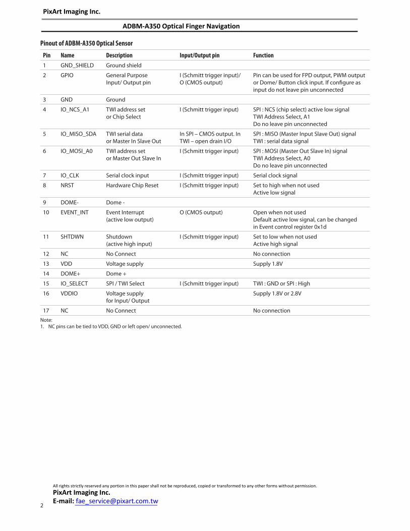
Pinout of ADBM-A350 Optical Sensor
Pin Name Description Input/Output pin Function
1 GND_SHIELD Ground shield
2 GPIO General Purpose Input/ Output pin
I (Schmitt trigger input)/ O (CMOS output)
Pin can be used for FPD output, PWM output or Dome/ Button click input. If confi gure as input do not leave pin unconnected
3 GND Ground
4 IO_NCS_A1 TWI address set or Chip Select
I (Schmitt trigger input) SPI : NCS (chip select) active low signalTWI Address Select, A1Do no leave pin unconnected
5 IO_MISO_SDA TWI serial data or Master In Slave Out
In SPI – CMOS output. In TWI – open drain I/O
SPI : MISO (Master Input Slave Out) signalTWI : serial data signal
6 IO_MOSI_A0 TWI address set or Master Out Slave In
I (Schmitt trigger input) SPI : MOSI (Master Out Slave In) signalTWI Address Select, A0Do no leave pin unconnected
7 IO_CLK Serial clock input I (Schmitt trigger input) Serial clock signal
8 NRST Hardware Chip Reset I (Schmitt trigger input) Set to high when not usedActive low signal
9 DOME- Dome -
10 EVENT_INT Event Interrupt (active low output)
O (CMOS output) Open when not usedDefault active low signal, can be changed in Event control register 0x1d
11 SHTDWN Shutdown (active high input)
I (Schmitt trigger input) Set to low when not usedActive high signal
12 NC No Connect No connection
13 VDD Voltage supply Supply 1.8V
14 DOME+ Dome +
15 IO_SELECT SPI / TWI Select I (Schmitt trigger input) TWI : GND or SPI : High
16 VDDIO Voltage supply for Input/ Output
Supply 1.8V or 2.8V
17 NC No Connect No connection
Note:1. NC pins can be tied to VDD, GND or left open/ unconnected.
PixArt Imaging Inc.
ADBM-A350 Optical Finger Navigation
All rights strictly reserved any portion in this paper shall not be reproduced, copied or transformed to any other forms without permission.
PixArt Imaging Inc. E-mail:

3
Figure 1. Package outline drawing
Pin #1
Pin #2
Pin #17
(∅4.00) Side Cut
7.20 0.10
Cover gate on either side(0.15mm max protrusion)
(For Connector)(1
9.00
)
5.40 0.15
8.20 0.50
8.20
0.5
0
23.1
0 0
.30
2X 0.30 Max
0.30
Max
(With Integrated Dome Switch & Actuator)
1.59 0.20
7.20
0.1
0
0.20 0.10(4.0
5)
3.84 0.20
Notes: 1. Dimension in millimeters.2. Dimensional tolerance: ±0.10mm.3. Maximum flash: ±0.2mm.4. Brackets () indicate reference dimensions.5. Document Number: ADBM-A350-G8_001
Recommended connector: FH26-17S-0.3SHW(05) HIROSE
PixArt Imaging Inc.
ADBM-A350 Optical Finger Navigation
All rights strictly reserved any portion in this paper shall not be reproduced, copied or transformed to any other forms without permission.
PixArt Imaging Inc. E-mail: [email protected]

4Not
e :-
Dom
e +
mus
t be
conn
ecte
d to
MCU
to d
etec
t but
ton
chan
ge s
tate
and
Dom
e –
can
be c
onne
cted
to G
ND
.
Figu
re 2
. Sch
emat
ic d
iagr
am fo
r in
terf
ace
betw
een
AD
BM
-A35
0 an
d 1.
8V m
icro
con
trol
ler
via
SPI
GN
D
IO_M
ISO
_SD
AIO
_MO
SI_
A0
IO_N
CS
_A1
IO_C
LK
IO_S
ELE
CT
DOME-
DOME+
1.8V microcontroller
0603
SW
2
SW
3
VD
D1.
8100k
1%
12
34
56
78
910
GN
D
GN
D
34
VD
D1.
8 C1
R2 10
nF
GN
D
112 2
LEFT
_SW
RIG
HT
_SW
R1
R5
100k
1%
0603
100k
1%
0603
VD
D1.
8
GN
D
VD
D1.
8
2
U1
100n
F/16
V06
03
C3
32.7
68K
Hz
X2
7 25 26 27 28 1 5 6 16 15
4VSS
RS
T/N
MI
P1.
4P
1.5
P1.
6P
1.7
TST
XO
UT
IXIN
P3.
5/R
XD
P3.
4/T
XD
VDD
P1.
0P
1.1
P1.
2P
1.3
P2.
5P
2.1
P2.
2P
2.3
P2.
4P
2.0
P3.
0P
3.6
P3.
7
P3.
2/M
ISO
P3.
3/C
LKP
3.1/
MO
SI
1221 22 23 24 3 9 10 19 20 8 11 17 18 13 14
EV
EN
T_I
NT
SH
TD
WN
NR
ST
VDDIO
1
GN
D
3
AD
BM
-A35
0
4 1165 7 10
VD
D2
D1
R9
1k
0603 G
RN
0805
GND
C4
R10
1uF/
16V
0805
0805
0603
220R D
2
1 2 3 4
U3 BQ
2420
0DG
N
MS
OP
-8
5678
351 2
IN VC
CS
TA
TV
SS
OU
TB
AT
CE N/C
1uF/
16V
0805
C19
1 2
D3 BA
T54C
SOT2
3 3
21
R19
R20
C25 1n
F06
03
51k
1%06
03
0603
51k
1% VS
S2
VS
S2
SW
6
CN
1 DA
TA
-
DA
TA
+
V + I D
GN
D
1 2 3 4 5
GND
VDD13
VD
D1.
8
8G
PIO
2 15
1uF
C20 08
05
VD
D1.
8
GN
D
LP29
89LV
-1.8
U5 OU
TP
UT
INP
UT
GND2
13
C22
C23
4.7u
F/10
V10
0nF
0603
0603
C21
100n
F06
03
NC12
NC
NC
16
NC17
C3
10nF
GN
D
C2
1uF
9
14

5
Regulatory Requirements
Passes FCC or CISPR 22 Class B emission limits when assembled following PixArt imaging recommendations.
Passes IEC 61000-4-3 and IEC61000-4-6 Class A Immunity limits when assembled following PixArt Imaging recommendations.
Absolute Maximum Ratings
Parameter Symbol Minimum Maximum Units Notes
Storage Temperature TS -40 85 °C
Analog and Digital Supply Voltage VDD -0.5 2.1 V
I/O Supply Voltage VDDIO -0.5 3.7 V
ESD (sensor only) 2 kV All pins, human body model JESD22-A114-E
Input Voltage VIN -0.5 VDD+0.5VDDIO+0.5
V
Latchup Current Iout 20 mA All Pins
Note: Stresses greater than those listed under “Absolute Maximum Ratings” may cause permanent damage to the device. These are the stress ratings only and functional operation of the device at these or any other condition beyond those indicated may aff ect device reliability.
Recommended Operating Conditions
Parameter Symbol Minimum Typical Maximum Units Notes
Operating Temperature TA -20 70 °C
Analog and Digital Supply Voltage [1]
VDD 1.7 1.8 2.1 Volts Including VNA noise.
I/O Supply Voltage [2] VDDIO 1.65 1.8 or 2.8 3.6 Volts Including VNA noise. Sets I/O voltages. See fi g 7.
Power Supply Rise Time tVRT 0.001 10 ms 0 to VDD. At minimum rise time, s/’
Power Supply Off Time for Valid POR (Power on Reset)
tOFF 10 ms Refer to section “POR During Power Cycling”
Power Off Voltage Level for Valid POR (Power on Reset)
VOFF 0 300 mV Refer to section “POR During Power Cycling”
Supply Noise (Sinusoidal) VNA 100 mV p-p 10 kHz - 50 MHz
Speed S 20 in/sec Using prosthetic fi nger as surface
Transient Supply Current IDDT 80 mA Max supply current for 500 sec for each supply voltages ramp from 0 to 1.8 V
Notes:1. Operating temperature of less than -20°C down to -30°C, minimum VDD of 1.8V must be met. 2. To ensure minimum leakage current, VDDIO should be greater than or equal to VDD
PixArt Imaging Inc.
ADBM-A350 Optical Finger Navigation
All rights strictly reserved any portion in this paper shall not be reproduced, copied or transformed to any other forms without permission.
PixArt Imaging Inc. E-mail: [email protected]

6
Timing Specifi cations
Electrical Characteristics over recommended operating conditions. Typical values at 25° C, VDD=VDDIO=1.8V.
Parameter Symbol Minimum Typical Maximum Units Notes
Motion Delay After Reset tMOT-RST 3.5 23 ms From Hard reset or SOFT_RESET register write to valid register write/read and motion, assuming motion is present
Shutdown tSHTDWN 50 ms From SHTDWN pin active to low current
Wake from Shutdown tWAKEUP 100 ms From SHTDWN pin inactive to valid motion. Refer to section “Notes on Shutdown”, also note tMOT-RST
EVENT_INT Rise Time tr-EVENT_INT 150 300 ns CL = 100 pF
EVENT_INT Fall Time tf-EVENT_INT 150 300 ns CL = 100 pF
SHTDWN Pulse Width tP-SHTDWN 150 ms
NRST Pulse Width tNRST 20 s From edge of valid NRST pulse
Reset Wait Time After Stable Supply Voltage
tVRT-NRST 100 ms
DC Electrical Specifi cations
Electrical Characteristics over recommended operating conditions. Typical values at 25° C, VDD=VDDIO=1.8V at default LED setting 13 mA.
Parameter Typical Max Units Notes
DC average supplycurrent in Run mode
IVDD 2.90 4.03 mA GPIO=SHTDWN=pull low, IO_MISO=NRST=pull high.
DC average supply current in Rest1 mode
IVDD 0.35 0.50 mA GPIO=SHTDWN=pull low, IO_MISO=NRST=pull high.
DC average supply current in Rest2 mode
IVDD 0.07 0.12 mA GPIO=SHTDWN=pull low, IO_MISO=NRST=pull high.
DC average supply current in Rest3 mode
IVDD 0.03 0.06 mA GPIO=SHTDWN=pull low, IO_MISO=NRST=pull high.
Analog shutdownsupply current
IDDSHTDWN VDD
1.54 26.0 A GPIO=pull low, SHTDWN=IO_MISO=NRST=pull high.
PixArt Imaging Inc.
!5.aπ!орл hLJǘƛŎŀƭ CƛƴƎŜNJ bŀǾƛƎŀǘƛƻƴ
All rights strictly reserved any portion in this paper shall not be reproduced, copied or transformed to any other forms without permission.
PixArt Imaging Inc. E-mail: [email protected]

7
DC Electrical Specifi cations
Electrical Characteristics over recommended operating conditions. Typical values at 25° C, VDD=VDDIO=1.8V at default LED setting 13 mA.
Parameter Symbol Minimum Typical Maximum Units Notes
VDDIO DC Supply Current I VDDIO 20 A
Digital peak supply current IPEAK VDD 10 mA
LED+ peak supply current IPEAK LED+ 35 mA At LED register setting of 27 mA
Input Low Voltage VIL -0.05 0 VDDIO*0.35 V IO_MOSI_A0, IO_CLK, IO_MISO_SDA, IO_NCS_A1, NRST, SHTDWN, IO_SELECT
Input High Voltage VIH VDDIO * 0.7 VDDIO VDDIO+0.05 V IO_MOSI_A0, IO_CLK, IO_MISO_SDA, IO_NCS_A1, NRST, SHTDWN, IO_SELECT
Input hysteresis VHYS 100 mV
Input leakage current Ileak ±1 ±10 A IO_MOSI_A0, IO_CLK, IO_MISO_SDA, IO_NCS_A1, NRST, SHTDWN, IO_SELECT
Output Low Voltage VOL 0.2 V Iout = 1.2 mA
Output High Voltage VOH VDDIO-0.2 VDDIO-0.1 V Iout = 600 A
Input Capacitance Cin 10 pF MOSI, NCS, SCLK, SHTDWN
Notes on Power-up Sequence
Below is the power up sequence for ADBM-A350:
1. Apply power.
2. Set NCS pin high, Shutdown pin low. Set IO_Select pin to low (for TWI) or high (for SPI).
3. If in TWI mode, set A0 and A1 according to the Table TWI slave address in datasheet. This step is skipped if SPI mode is used.
4. Read Product ID to ensure sensor is powered up and communicating properly with host.
5. Write 0xC9 to address 0x61.
Note on register settings
Please refer to the OFN A350 fi rmware design guide for tuning of Speed Switching, Assert/De-assert, Finger Presence Detect and XY Quantization register settings.
Notes on Shutdown and Reset
The ADBM-A350 can be set in Shutdown mode by asserting or setting SHTDWN pin high. During the shutdown state, supply voltages VDD must be maintained above the minimum level. If these conditions are not met, then the sensor must be restarted by powering down then powering up again for proper operation. Any register settings must then be reloaded.
During the shutdown state, supply voltage VDD must be maintained above the minimum level. For proper operation, SHTDWN pulse width must be at least tP-SHTDWN.
Shorter pulse widths may cause the chip to enter an undefi ned state. In addition, the SPI or TWI port of the sensor should not be accessed when SHTDWN is asserted. Other devices on the same SPI bus can be accessed, as long as the sensor’s NCS pin is not asserted. The table below shows the state of various pins during shutdown. After deasserting SHTDWN, wait tWAKEUP before accessing the SPI port. Reinitializing the sensor from shutdown state will retain all register data that were written to the sensor prior to shutdown.
The reset of the sensor via SOFT_RESET register or through the NRST pin would reset all registers to the default value. Any register settings must then be reloaded.
Pin SHTDWN active
IO_NCS_A1 Functional
IO_MISO_SDA Undefi ned
IO_CLK Undefi ned
IO_MOSI_A0 Undefi ned
XY_LED Low current
EVENT_INT Undefi ned
NRST High
IO_Select SPI: High, TWI: Low
GPIO Undefi ned Note: There are long wakeup times from shutdown. These features should not be used for power management during normal sensor motion.
PixArt Imaging Inc.
!5.aπ!орл hLJǘƛŎŀƭ CƛƴƎŜNJ bŀǾƛƎŀǘƛƻƴ
All rights strictly reserved any portion in this paper shall not be reproduced, copied or transformed to any other forms without permission.
PixArt Imaging Inc. E-mail: [email protected]

8
Power on Reset (POR) During Power Cycling
tVRT is the power supply (VDD) rise time specifi cation for a valid power on reset to happen when the sensor is powered up from 0V to VDD. At condition whereby the VDD of the sensor is cycled from VDD to 0 V and then to VDD again, the two parameters that govern a valid power on reset are vOFF and tOFF. Refer to timing diagram below.
Figure 3. Power on Reset during power cycling
tVRT
0V
VDD
tVRTtOFF
VDD
vOFF 0V
Power management modes
The ADBM-A350 has three power-saving modes. Each mode has a diff erent motion detection period, aff ecting response time to sensor motion (Response Time). The sensor automatically changes to the appropriate mode, depending on the time since the last reported motion (Downshift Time). The parameters of each mode are shown in the following table.
Mode Response Time
(nominal)
Downshift Time
(nominal)
Rest 1 19.5 ms 250 ms
Rest 2 96 ms 9.5 s
Rest 3 482 ms 582 s
EVENT_INT Pin
The Event_Int pin is a level-sensitive interrupt output that is used to trigger the host micro-controller when one of these events occurs:
FPD – A change in fi nger state (fi nger on to fi nger off and vice versa) is detected
Soft Click – Soft Click is detected
Button – Mechanical button is asserted or de-asserted
Motion – Motion delta is present.
A read to event register is required to determine the specifi c event that toggles the interrupt for user to act upon.
The EVENT_INT will be reset after the user responds to it by reading the respective event status register:
FPD – reading FPD_STATUS register (0x7a)
Soft Click – reading SC_STATUS register (0x7f )
Button – reading BUTTON_STATUS register (0x12)
Motion – reading DELTA_X and DELTA_Y registers until motion are cleared.
GPIO Pin
The GPIO pin is a level-sensitive input/ output that can be used as
FPD output – to display FPD status
Pulse Width Modulated (PWM) output – to control LED driver to enable illumination feature in a product eg mobile phone
Dome/ Button click input – can be connected to a dome switch that provides an input to the sensor and when a click is detected, sensor can respond by trigger-ing button interrupt and channel the interrupt status through EVENT pin.
Refer to A350 Firmware Design Guide for more details and settings of registers for these features.
LED Mode
For power savings, the LED will not be continuously on. ADBM-A350 will fl ash the LED only when needed.
PixArt Imaging Inc.
!5.aπ!орл hLJǘƛŎŀƭ CƛƴƎŜNJ bŀǾƛƎŀǘƛƻƴ
All rights strictly reserved any portion in this paper shall not be reproduced, copied or transformed to any other forms without permission.
PixArt Imaging Inc. E-mail: [email protected]

9
Bit(s) Name Reset Description Remarks
7:6 NRST_STATE 0x0 0x0: unknown
0x1: Low Invalid as the chip will be in reset state.
0x2: High
0x3: Hi-Z Indicate a fl oating high
5:4 SHUTDOWN_STATE 0x0 0x0: unknown
0x1: Low
0x2: High Invalid as the chip will be in shutdown state.
0x3: Hi-Z Indicate a fl oating low
3:2 GPIO_STATE 0x0 0x0: unknown
0x1: Low
0x2: High
0x3: Hi-Z
1:0 IO_SELECT_STATE 0x0 0x0: unknown
0x1: Low
0x2: High
0x3: Hi-Z
For output pins (EVENT_INT, GPIO, MOSI and MISO) testing, fi rst enable bit-4 of PAD_FUNCTION (0x34) register. Then program or set the output state via PAD_TEST_OUT register (0x33) and do a READ on the actual pin status. Actual pin status results should match the output set in PAD_TEST_OUT. (Note: SPI/TWI communica-tion will be disabled after this test is enabled. Once this test is completed, an external hardware reset on sensor is required)
I/O Pin Status Test
This feature allows the user to verify the connectivity and the state of the I/O pin.
To run the test for input pins such as GPIO, SHUTDOWN, NRST and IO_SELECT, fi rst enable the PAD_Chk_On bit (or bit-1) of OFN_ENGINE2 (0x61) register. Then write any value to PAD_STATUS (0x31) register to start the test. Wait for ap-proximately 12us before reading the actual pin status and PAD_STATUS register. The test will be considered a PASS to indicate the sensor is responding accordingly if the actual pin status matches PAD_STATUS register content. Refer to the table below for I/O pin status defi nition.
PixArt Imaging Inc.
!5.aπ!орл hLJǘƛŎŀƭ CƛƴƎŜNJ bŀǾƛƎŀǘƛƻƴ
All rights strictly reserved any portion in this paper shall not be reproduced, copied or transformed to any other forms without permission.
PixArt Imaging Inc. E-mail: [email protected]

10
Figure 4. Output pin status and Frame Start
ADBM-A350 comes with a unique feature that enables user to capture the image the optical sensor is seeing on the tracking surface. This is achieved through storing the pixel data, transferring or dumping the pixels data out to the host for processing and rebuilding the dumpThe rebuilding of dump is mainly coneach 8-bit pixel data to form a grayscale digital image.
Some useful applications for this feature are sensor con-tamination inspection at manufacturing lines, image rec-ognition, motion sensing applications and etc.
The host will connect to the OFN sensor and send the following register commands to initiate dump. The following procedure is outlined below.
1. Sensor power up.
2. Read sensor address 0x00 for correct product ID or PID.
3. Write sensor address 0x3a with 0x5a hex.
4. Provide a 24 MHz clock into GPIO pin at VDDIO level.
5. Write sensor address 0x28 with 0x01 hex.
6. Sensor will start to dump with frame start for ~500 ms.
7. Write sensor address 0x3a with 0x5a hex to perform soft reset or perform a hard reset to reset sensor back to normal operation.
There are several signals which need to be tapped. They are namely EVENT_INT, MISO_SDA and GPIO pin of the sensor. GPIO will be input while MISO_SDA and EVENT_INT are the output pins that the host controller must interface to the sensor, readout the data and then build the dump
Pin Status Description
GPIO Input 24MHz clock signal
MISO_SDA Output Pixel data bits 7 to 4
EVENT_INT Output Pixel data bits 3 to 0
Referenced to Figure 10 above, the sensor will output signals based on the 24 MHz clock signal via the GPIO pin. Executing the sequence of register setting outlined in
Dump Commands above will initiate dump. After step #6, each MISO_SDA pin and EVENT_INT pin will go high for 4 clock cycles. This indicates pixel frame start. Then after 4 clock cycles, MISO_SDA pin will go low and EVENT_INT pin is still high. This indicates pixel begin state.
The pixel bits will start to clock thereafter. Each pixel is represented by an 8-bit data or value. MISO_SDA pin will output the most signifi cant bits D7 to D4 and Motion pin will output the least signifi cant bits D3 to D0. Then a pixel end state (a high in MISO_SDA and low in EVENT_INT) will follow. This completes the fi rst pixel address 0 data. The next pixel address 1 data is then clocked out with a pixel begin state, 4 clock cycles of data followed by a pixel end state in the same manner. This will continue until all the 361 pixels (19x19 pixel array) data is read.
PixArt Imaging Inc.
!5.aπ!орл hLJǘƛŎŀƭ CƛƴƎŜNJ bŀǾƛƎŀǘƛƻƴ
All rights strictly reserved any portion in this paper shall not be reproduced, copied or transformed to any other forms without permission.
PixArt Imaging Inc. E-mail: [email protected]

11
Below is the pixel array address map. The fi gure shows the view of the chip from the top of the OFN aperture. Rows are read from top to bottom and columns from left to right.
Figure 5. Frame End
Note: It is advisable to have a counter at the Host to keep count of the number of pixel addresses and data byte. If the number of pixel data byte does not correspond to the sensor number of pixel then this dump data is invalid. In this case the sensor must be reset and a new dump must be initiated.
Pixel byte format
Bit 8 Bit 7 Bit 6 Bit 5 Bit 4 Bit 3 Bit 2 Bit1
D7 D6 D5 D4 D3 D2 D1 D0
Pin 1
0 1 2 3 4 5 6 7 8 9 10 11 12 13 14 15 16 17 18
19 20 21 22 23 24 25 26 27 28 29 30 31 32 33 34 35 36 37
38 39 40 41 42 43 44 45 46 47 48 49 50 51 52 53 54 55 56
57 58 59 60 61 62 63 64 65 66 67 68 69 70 71 72 73 74 75
76 77 78 79 80 81 82 83 84 85 86 87 88 89 90 91 92 93 94
95 96 97 98 99 100 101 102 103 104 105 106 107 108 109 110 111 112 113
114 115 116 117 118 119 120 121 122 123 124 125 126 127 128 129 130 131 132
133 134 135 136 137 138 139 140 141 142 143 144 145 146 147 148 149 150 151
152 153 154 155 156 157 158 159 160 161 162 163 164 165 166 167 168 169 170
171 172 173 174 175 176 177 178 179 180 181 182 183 184 185 186 187 188 189
190 191 192 193 194 195 196 197 198 199 200 201 202 203 204 205 206 207 208
209 210 211 212 213 214 215 216 217 218 219 220 221 222 223 224 225 226 227
228 229 230 231 232 233 234 235 236 237 238 239 240 241 242 243 244 245 246
247 248 249 250 251 252 253 254 255 256 257 258 259 260 261 262 263 264 265
266 267 268 269 270 271 272 273 274 275 276 277 278 279 280 281 282 283 284
285 286 287 288 289 290 291 292 293 294 295 296 297 298 299 300 301 302 303
304 305 306 307 308 309 310 311 312 313 314 315 316 317 318 319 320 321 322
323 324 325 326 327 328 329 330 331 332 333 334 335 336 337 338 339 340 341
342 343 344 345 346 347 348 349 350 351 352 353 354 355 356 357 358 359 360
Pin 18
The signal to indicate the end of the dump frame is shown in Figure 10 below where pix end state is followed by a low in both MISO_SDA and EVENT_INT. This will inform the Host of the pixel end and frame end state.
PixArt Imaging Inc.
!5.aπ!орл hLJǘƛŎŀƭ CƛƴƎŜNJ bŀǾƛƎŀǘƛƻƴ
All rights strictly reserved any portion in this paper shall not be reproduced, copied or transformed to any other forms without permission.
PixArt Imaging Inc. E-mail: [email protected]

12
4-wire Serial Peripheral Interface (SPI)
SPI Specifi cations
Electrical Characteristics over recommended operating conditions. Typical values at 25° C, VDD = 1.8 V.
Parameter Symbol Minimum Typical Maximum Units Notes
Serial Port Clock Frequency
fsclk 1 MHz Active drive, 50% duty cycle
MISO rise time tr-MISO 150 300 ns CL = 100 pF
MISO fall time tf-MISO 150 300 ns CL = 100 pF
MISO delay after SCLK tDLY_MISO 120 ns From SCLK falling edge to MISO data valid, no load conditions
MISO hold time thold_MISO 0.5 1/fSCLK μs Data held until next falling SCLK edge
MOSI hold time thold_MOSI 200 ns Amount of time data is valid after SCLK rising edge
MOSI setup time tsetup_MOSI 120 ns From data valid to SCLK rising edge
SPI time between write commands
tSWW 30 s From rising SCLK for last bit of the fi rst data byte, to rising SCLK for last bit of the second data byte.
SPI time between write and read commands
tSWR 20 s From rising SCLK for last bit of the fi rst data byte, to rising SCLK for last bit of the second address byte.
SPI time between read and subsequent commands
tSRWtSRR
500 ns From rising SCLK for last bit of the fi rst data byte, to falling SCLK for the fi rst bit of the address byte of the next command.
SPI read address-data delay
tSRAD 4 s From rising SCLK for last bit of the address byte, to falling SCLK for fi rst bit of data being read.
NCS inactive after motion burst
tBEXIT 500 ns Minimum NCS inactive time after motion burst before next SPI usage
NCS to SCLK active tNCS-SCLK 120 ns From NCS falling edge to fi rst SCLK falling edge
SCLK to NCS inactive (for read operation)
tSCLK-NCS 120 ns From last SCLK rising edge to NCS rising edge, for valid MISO data transfer
SCLK to NCS inactive (for write operation)
tSCLK-NCS 20 us From last SCLK rising edge to NCS rising edge, for valid MOSI data transfer
NCS to MISO high-Z tNCS-MISO 500 ns From NCS rising edge to MISO high-Z state
PixArt Imaging Inc.
!5.aπ!орл hLJǘƛŎŀƭ CƛƴƎŜNJ bŀǾƛƎŀǘƛƻƴ
All rights strictly reserved any portion in this paper shall not be reproduced, copied or transformed to any other forms without permission.
PixArt Imaging Inc. E-mail: [email protected]

13
Chip Select Operation
The serial port is activated after NCS goes low. If NCS is raised during a transaction, the entire transaction is aborted and the serial port will be reset. This is true for all transactions. After a transaction is aborted, the normal address-to-data or transaction-to-transaction delay is still required before beginning the next transaction. To improve communication reliability, all serial transactions should be framed by NCS. In other words, the port should not remain enabled during periods of non-use because ESD events could be interpreted as serial communica-tion and put the chip into an unknown state. In addition, NCS must be raised after each burst-mode transaction is complete to terminate burst-mode. The port is not available for further use until burst-mode is terminated.
Write Operation
Write operation, defi ned as data going from the micro-controller to the ADBM-A350, is always initiated by the micro-controller and consists of two bytes. The fi rst byte contains the address (seven bits) and has a “1” as its MSB to indicate data direction. The second byte contains the data. The ADBM-A350 reads MOSI on rising edges of SCLK.
MOSI Driven by Micro-Controller
Do not care
A6 A5 A4 A3 A2 A1 A0 D7 D6 D5 D4 D3 D2 D1 D0
157 8 9 10 11 12 13 14 162 3 4 5 6
1 A61
SCLK
MOSI
1 1 2
NCS
MISO
SCLK
MOSI
tsetup , MOSI
tHold,MOSI
Figure 6. Write Operation
Figure 7. MOSI Setup and Hold Time
Synchronous Serial Port
The synchronous serial port is used to set and read para-meters in the ADBM-A350, and to read out the motion information.
The port is a four wire serial port. The host micro-controller always initiates communication; the ADBM-A350 never initiates data transfers. SCLK, MOSI, and NCS may be driven directly by a micro-controller. The port pins may be shared with other SPI slave devices. When the NCS pin is high, the inputs are ignored and the output is tri-stated.
The lines that comprise the 4-wire SPI port:
SCLK: Clock input. It is always generated by the master (the micro-controller).
MOSI: Input data. (Master Out/Slave In)
MISO: Output data. (Master In/Slave Out)
NCS: Chip select input (active low). NCS needs to be low to activate the serial port; otherwise, MISO will be high Z, and MOSI & SCLK will be ignored. NCS can also be used to reset the serial port in case of an error.
PixArt Imaging Inc.
!5.aπ!орл hLJǘƛŎŀƭ CƛƴƎŜNJ bŀǾƛƎŀǘƛƻƴ
All rights strictly reserved any portion in this paper shall not be reproduced, copied or transformed to any other forms without permission.
PixArt Imaging Inc. E-mail: [email protected]

14
Read Operation
A read operation, defi ned as data going from the ADBM-A350 to the micro-controller, is always initiated by the micro-controller and consists of two bytes. The fi rst byte contains the address, is sent by the micro-controller over MOSI, and has a “0” as its MSB to indicate data direction. The second byte contains the data and is driven by the ADBM-A350 over MISO. The sensor outputs MISO bits on falling edges of SCLK and samples MOSI bits on every rising edge of SCLK.
tr-MISO
SCLK
MISO D0
tHOLD-MISOtDLY-MISO
tf-MISO
Figure 8. Read Operation
Figure 9. MISO Delay and Hold Time
NOTE: The 0.5/fSCLK minimum high state of SCLK is also the minimum MISO data hold time of the ADBM-A350. Since the falling edge of SCLK is actually the start of the next read or write command, the ADBM-A350 will hold the state of data on MISO until the falling edge of SCLK.
Required timing between Read and Write Commands
There are minimum timing requirements between read and write commands on the serial port.
SCLK
Address Data
tSWW
Write Operation
Address Data
Write Operation
Figure 10. Timing between two write commands
If the rising edge of the SCLK for the last data bit of the second write command occurs before the required delay (tSWW), then the fi rst write command may not complete correctly.
Address Data
Write Operation
Address
Next ReadOperation
SCLK
tSWR
Figure 11. Timing between write and read commands
1 2 3 4 5 6 7 8SCLKCycle #
SCLK
MOSI 0 A6 A5 A4 A3 A2 A1 A0
9 10 11 12 13 14 15 16
MISO D6 D5 D4 D3 D2 D1 D0D7
NCS
tSRAD delay
Do not care
PixArt Imaging Inc.
!5.aπ!орл hLJǘƛŎŀƭ CƛƴƎŜNJ bŀǾƛƎŀǘƛƻƴ
All rights strictly reserved any portion in this paper shall not be reproduced, copied or transformed to any other forms without permission.
PixArt Imaging Inc. E-mail: [email protected]
15
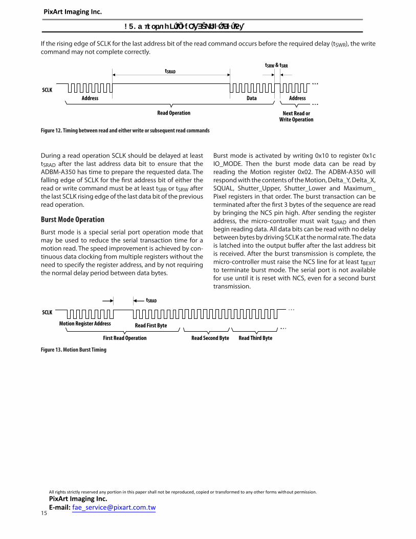
If the rising edge of SCLK for the last address bit of the read command occurs before the required delay (tSWR), the write command may not complete correctly.
Next Read orWrite Operation
Data
tSRAD
Read Operation
Address
tSRW & tSRR
Address
SCLK
Figure 12. Timing between read and either write or subsequent read commands
During a read operation SCLK should be delayed at least tSRAD after the last address data bit to ensure that the ADBM-A350 has time to prepare the requested data. The falling edge of SCLK for the fi rst address bit of either the read or write command must be at least tSRR or tSRW after the last SCLK rising edge of the last data bit of the previous read operation.
Burst Mode Operation
Burst mode is a special serial port operation mode that may be used to reduce the serial transaction time for a motion read. The speed improvement is achieved by con-tinuous data clocking from multiple registers without the need to specify the register address, and by not requiring the normal delay period between data bytes.
Burst mode is activated by writing 0x10 to register 0x1c IO_MODE. Then the burst mode data can be read by reading the Motion register 0x02. The ADBM-A350 will respond with the contents of the Motion, Delta_Y, Delta_X, SQUAL, Shutter_Upper, Shutter_Lower and Maximum_Pixel registers in that order. The burst transaction can be terminated after the fi rst 3 bytes of the sequence are read by bringing the NCS pin high. After sending the register address, the micro-controller must wait tSRAD and then begin reading data. All data bits can be read with no delay between bytes by driving SCLK at the normal rate. The data is latched into the output buff er after the last address bit is received. After the burst transmission is complete, the micro-controller must raise the NCS line for at least tBEXIT to terminate burst mode. The serial port is not available for use until it is reset with NCS, even for a second burst transmission.
Motion Register Address Read First Byte
First Read Operation Read Second Byte
SCLK
tSRAD
Read Third Byte
Figure 13. Motion Burst Timing
PixArt Imaging Inc.
!5.aπ!орл hLJǘƛŎŀƭ CƛƴƎŜNJ bŀǾƛƎŀǘƛƻƴ
All rights strictly reserved any portion in this paper shall not be reproduced, copied or transformed to any other forms without permission.
PixArt Imaging Inc. E-mail: [email protected]

16
Two – Wire Interface (TWI)
ADBM-A350 uses a two-wire serial control interface compatible with I2C. The parameters are listed below.
TWI Specifi cations
Electrical Characteristics over recommended operating conditions. Typical values at 25° C, VDD = 1.8 V.
Parameter Symbol Minimum Maximum Units Notes
SCL clock frequency fscl 400 kHz
Hold time (repeated) START condition. After this period, the fi rst clock pulse is generated
tHD_STA 0.6 – s
LOW period of the SCL clock tLOW 1.0 – s
HIGH period of the SCL clock tHIGH 0.6 – s
Set up time for a repeated START condition tSU_STA 0.6 – s
Data hold time tHD_DAT 0(2) 0.9(3) s
Data set-up time tSU_DAT 100 – ns
Rise time of both SDA and SCL signals tr 20+0.1Cb(4) 300 ns
Fall time of both SDA and SCL signals tf 20+0.1Cb(4) 300 ns
Set up time for STOP condition tSU_STO 0.6 – s
Bus free time between a STOP and START condition tBUF 1.3 – s
Capacitive load for each bus line Cb – 400 pF
Noise margin at the LOW level for each connected device (including hysteresis)
VNL 0.1 VDD – V
Noise margin at the HIGH level for each connected device (including hysteresis)
VNH 0.2 VDD V
Notes:1. All values referred to VIHMIN and VILMAX levels. 2. A device must internally provide a hold time of at least 300 ns for the SDA signal (referred to the VIHMIN of the SCL signal) to bridge the undefi ned
region of the falling edge of SCL. 3. The maximum has tHD_DAT only to be met if the device does not stretch the LOW period (tLOW) of the SCL signal.4. CB = total capacitance of one bus line in pF.
The ADBM-A350 responds to one of the following select-able slave device addresses depending on the IO_MOSI_A0 and IO_NCS_A1 input pin state. These pins should be set to avoid confl ict with any other devices that might be sharing the bus.
Table 1. TWI slave address
A0 A1 Slave Address (Hex)
0 0 33
0 1 3b
1 0 53
1 1 57
Serial Transfer Clock and Serial Data signals
The serial control interface uses two signals: a serial transfer clock (SCL) signal and a serial data (SDA) signal. Always driven by the master, SCL synchronizes the serial transmission of data bits on SDA. The frequency of SCL may vary throughout a transfer, as long as the timing is greater than the minimum timing.
SDA is bi-directional. The host (master) can read from or write to the ADBM-A350. The host (typically a microcon-troller) drives SCL and SDA in a write operation or request-ing information from the ADBM-A350. The ADBM-A350 drives the SDA only under two conditions. First, when re-sponding with an acknowledge (ACK) bit after receiving data from the host, or second, when sending data to the host at the host’s request. Data is sent in Eight-bit packets.
PixArt Imaging Inc.
!5.aπ!орл hLJǘƛŎŀƭ CƛƴƎŜNJ bŀǾƛƎŀǘƛƻƴ
All rights strictly reserved any portion in this paper shall not be reproduced, copied or transformed to any other forms without permission.
PixArt Imaging Inc. E-mail: [email protected]

17
Figure 14. TWI Start and Stop operation
Acknowle dge/Not Acknowledge Bit
After a start condition, a single acknowledge/not acknowledge bit follows each Eight-bit data packet. The device receiving the data drives the acknowledge/not acknowledge signal on SDA. Acknowledge (ACK) is defi ned as 0 and not acknowledge (NAK) is defi ned as 1.
Packet Formats
Read and write operations between the host and the ADBM-A350 use three types of host driven packets and one type of ADBM-A350 driven packet. All packets are eight bits long with the most signifi cant bit fi rst, followed by an acknowledge bit.
Slave Device Address (DA)
Command packets contain a 7-bit ADBM-A350 device address and an active low read/write bit (R/W).
Last bit ofpacket
DA[6] DA[4] DA[3] DA[2] DA[1] DA[0] Write = 0Read = 1
Device Address
DA[5]
First bit ofpacket
R/W
Register Address Packets (RA)
The address packets contain an auto-increment (ai) bit and a 7-bit address. If the ‘ai’ bit is set, the slave will process data from successive addresses in successive bytes. For example, registers 0x01, 0x02, and 0x03 can be written by setting the ‘ai’ bit to one with address 0x01. The host would send three bytes of data, and the host would terminate with a P condition.
RA[6] RA[5] RA[4] RA[3] RA[2] RA[1] RA[0]Autoincrement=1,
Noincrement=0
Autoincrement
First bit ofpacket
Last bit ofpacket
Register Address
START Condition STOP Condition
SCL driven by host
SDA driven by host
SDA falls whileSCL is high
SDA rises whileSCL is high
Start and St op of Synchronous Operation
The host initiates and terminates all data transfers. Data transfers are initiated by driving SDA from high to low while holding SCL high. Data transfers are terminated by driving SDA from low to high while SCL is held high.
PixArt Imaging Inc.
!5.aπ!орл hLJǘƛŎŀƭ CƛƴƎŜNJ bŀǾƛƎŀǘƛƻƴ
All rights strictly reserved any portion in this paper shall not be reproduced, copied or transformed to any other forms without permission.
PixArt Imaging Inc. E-mail: [email protected]

18
Data Packet (DP)
Contains 8 data bits and may be sent by the host or the ADBM-A350.
Last bit ofpacket
DP[7] DP[5] DP[4] DP[3] DP[2] DP[1] DP[0]
Data
DP[6]
First bit ofpacket
Host Driven Packets
The host initiates all data transmission with a START condition. Next, slave address and register address packets are sent. If there is a device address match, the ADBM-A350 then responds to each Eight-bit data trans-mission with an acknowledge signal (SDA = 0). Data is transmitted with the most signifi cant bit fi rst.
Figure 15. Host packets
To terminate the transfer of host driven packets, the host follows the ADBM-A350’s ACK with a STOP condition. The host can also issue a START condition after the ADBM-A350’s ACK if it wants to start a new data transfer.
SCL driven by host
SDA
Start
STOP or STARTCondition
Module must respond after eachdata byte with a 1-bit 0-valued
acknowledge (ACK)
Host terminates datatransmission by following
the ACK with a STOPcondition or another
START condition
HostDriven
ADBSDriven
Host DrivenPacket
ADBSDriven
Host DrivenPacket
ACKD0D6–D1
ACK
ACK
7 6 – 1 0
D7 D0
ACK7 6 – 1 0
D7
Not acknowledging (NAK)signals indicate an error
condition
PixArt Imaging Inc.
!5.aπ!орл hLJǘƛŎŀƭ CƛƴƎŜNJ bŀǾƛƎŀǘƛƻƴ
All rights strictly reserved any portion in this paper shall not be reproduced, copied or transformed to any other forms without permission.
PixArt Imaging Inc. E-mail: [email protected]

19
Figure 16. Sensor packets
Example: Writing Data to Sensor Registers
The host writes a value of 0x02 to address 0x07 in the following illustration.
The example ADBM-A350 address is 0x57.
START
1 2 3
DA RA DP
0000111 00000010
ACK ACK
STOP
ACK
Packet type
Packet Number
SDAhost
SDAADBS
1010111
ADBSAddress 0 x 57
Register Address 0 x 07
Data 0 x 02
7 0
0 0
7 0 7 0
aiR/W
Figure 17. TWI write
SCL driven by host
SDA
ACK
STOP or STARTCondition
The host terminates datatransmission by responding
with a not acknowledge (NAK), followed by a STOP
condition or another STARTcondition
HostDriven
ADBS DrivenPacket
HostDriven
ADBS DrivenPacket
NAKD0D6–D1D6–D1
ACK
ACK
7 6 – 1 0
D7 D0
NAK7 6 – 1 0
D7
If the host responds withan acknowledge (ACK),
the ADBS sends anotherdata byte
ADBM-A350 Driven Packets
By request of the host, the ADBM-A350 acknowledges a read request and then outputs a data byte transmitting the most signifi cant bit (7) fi rst. If the host intends to continue the data transfer, the host acknowledges the ADBM-A350. If the host intends to terminate the transfer, it responds with not acknowledge (SDA = 1), and then drives SDA to generate a STOP condition. The host can also drive a START condition if it wants to begin a new data transfer with the same ADBM-A350.
PixArt Imaging Inc.
!5.aπ!орл hLJǘƛŎŀƭ CƛƴƎŜNJ bŀǾƛƎŀǘƛƻƴ
All rights strictly reserved any portion in this paper shall not be reproduced, copied or transformed to any other forms without permission.
PixArt Imaging Inc. E-mail: [email protected]

20
Example: Single Byte Read from Sensor Register
The sensor reads a value 0x01from the register address 0x02 in the following illustration. Again, the example ADBM-A350 address is 0x57.
1 2
DA RA
START 00
ACK ACK
1010111 0000010
Register Address0 x 02
ADBSAddress 0 x 57
Packet number
Packet type
SDAhost
SDAADBS
3 4
DA DP
START NAK
ACK
STOP
00000001
1010 111
ADBSAddress 0 x 57 Data 0 x 01
7 0
1
R/W 7 0
Packetnumber
Packettype
SDAhost
SDAADBS
Host could
also drive
another
START
condition
instead of a
STOP
condition
7 0 7 0
R/W ai
Figure 18. TWI single byte read
PixArt Imaging Inc.
!5.aπ!орл hLJǘƛŎŀƭ CƛƴƎŜNJ bŀǾƛƎŀǘƛƻƴ
All rights strictly reserved any portion in this paper shall not be reproduced, copied or transformed to any other forms without permission.
PixArt Imaging Inc. E-mail: [email protected]
21
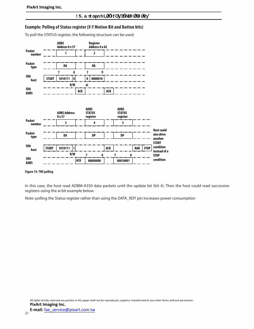
Example: Polling of Status register (X-Y Motion Bit and Button bits)
To poll the STATUS register, the following structure can be used:
1 2
DA RA
START 00000101010111
7 7 00
0 0
ADBSAddress 0 x 57
RegisterAddress 0 x 02
ACK ACK
R/W ai
Packet number
Packettype
SDAhost
SDA
ADBS
3 4
DA DP
5
DP
START ACK NAK STOP
ACK 00010001
1010111
R/W 7 0
00000000
Host could
also drive
another
START
condition
instead of a
STOP
condition
Packet number
Packettype
SDA host
SDA
ADBS
ADBS Address0 x 57
ADBSSTATUSregister
ADBSSTATUSregister
7 0
1
Figure 19. TWI polling
In this case, the host read ADBM-A350 data packets until the update bit (bit 4). Then the host could read successive registers using the ai bit example below.
Note: polling the Status register rather than using the DATA_RDY pin increases power consumption
PixArt Imaging Inc.
!5.aπ!орл hLJǘƛŎŀƭ CƛƴƎŜNJ bŀǾƛƎŀǘƛƻƴ
All rights strictly reserved any portion in this paper shall not be reproduced, copied or transformed to any other forms without permission.
PixArt Imaging Inc. E-mail: [email protected]

22
Example: Multiple-Byte Read from Sensor Register using ‘ai’ bit
The ai is a useful feature, especially in the case of reading Delta_X, Delta_Y, and Delta_HI in succession once either the DATA_RDY interrupt pin and/or update bit in the STATUS register bit are set.
Once the ai bit is set, the slave will deliver data packets from successive addresses until the ‘STOP’ condition from the host.
In the example below, 3 bytes are read successively from registers 0x03, 0x04, and 0x05.
Figure 20. TWI ai bit
1 2
DA RA
START 1 0000011
ACK ACK
1010111
R/W ai
7 0
0
7 0
Packetnumber
Packettype
SDAhost
SDAADBS
3
DA
START
4 5 6
DP DP DP
ACK ACK NAK
ACK 10101101 00000001 10000101
1010111 STOP
R/W 7 0 7 0
Packetnumber
Packettype
SDA host
SDAADBS
Host could also drive another START condition instead of a STOP condition
ADBS Address0 x 57
Register Address0 x 03
ADBSAddress 0 x 57
ADBS Datafrom address0 x 03
ADBS Datafrom address0 x 04
ADBS Datafrom address0 x 05
7 0
1
PixArt Imaging Inc.
!5.aπ!орл hLJǘƛŎŀƭ CƛƴƎŜNJ bŀǾƛƎŀǘƛƻƴ
All rights strictly reserved any portion in this paper shall not be reproduced, copied or transformed to any other forms without permission.
PixArt Imaging Inc. E-mail: [email protected]

23
ADBM-A350 driven SDA
SCL and SDA Timing
Figure 21. TWI SCL and SDA Timing
Figure 22. Sensor driven SDA
SCL driven by host
SDA driven by hostor ADBS
Data Hold time Data Propagation time
SCL driven by host
SDA driven by host or ADBS
SDA sampled after the rising edge of SCL
SDA driven after the falling edge of SCL
Clock Low Clock High
SCL drivenby host
SDA drivenby host
Data Set-up time(minimum 0 ns)
PixArt Imaging Inc.
!5.aπ!орл hLJǘƛŎŀƭ CƛƴƎŜNJ bŀǾƛƎŀǘƛƻƴ
All rights strictly reserved any portion in this paper shall not be reproduced, copied or transformed to any other forms without permission.
PixArt Imaging Inc. E-mail: [email protected]

24
Registers
The ADBM-A350 registers are accessible via the serial port. The registers are used to read motion data and status as well as to set the device confi guration.
Address Register
Read/
Write
Default
Value Address Register
Read/
Write
Default
Value
0x00 Product_ID R 0x88 0x40-0x5f Reserved
0x01 Revision_ID R 0x00 0x60 OFN_Engine1 R/W 0x84
0x02 EVENT R/W Any 0x61 OFN_Engine2 R/W 0x89
0x03 Delta_X R Any 0x62 Resolution R/W 0x22
0x04 Delta_Y R Any 0x63 Speed_Ctrl R/W 0x0e
0x05 SQUAL R Any 0x64 Speed_ST12 R/W 0x08
0x06 Shutter_Upper R Any 0x65 Speed_ST21 R/W 0x06
0x07 Shutter_Lower R Any 0x66 Speed_ST23 R/W 0x40
0x08 Maximum_Pixel R Any 0x67 Speed_ST32 R/W 0x08
0x09 Pixel_Sum R Any 0x68 Speed_ST34 R/W 0x48
0x0a Minimum_Pixel R Any 0x69 Speed_ST43 R/W 0x0a
0x0b Pixel_Grab R/W Any 0x6a Speed_ST45 R/W 0x50
0x0c CRC0 R 0x00 0x6b Speed_ST54 R/W 0x48
0x0d CRC1 R 0x00 0x6c GPIO_CTRL R/W 0x80
0x0e CRC2 R 0x00 0x6d AD_CTRL R/W 0xc4
0x0f CRC3 R 0x00 0x6e AD_ATH_HIGH R/W 0x3a
0x10 Reserved W 0x00 0x6f AD_DTH_HIGH R/W 0x40
0x11 Reserved 0x70 AD_ATH_LOW R/W 0x35
0x12 BUTTON_STATUS R/W 0x00 0x71 AD_DTH_LOW R/W 0x3b
0x13 Run_Downshift R/W 0x04 0x72 QUANTIZE_CTRL R/W 0x99
0x14 Rest1_Period R/W 0x01 0x73 XYQ_THRESH R/W 0x02
0x15 Rest1_Downshift R/W 0x1f 0x74 MOTION_CTRL R/W 0x00
0x16 Rest2_Period R/W 0x09 0x75 FPD_CTRL R/W 0xfa
0x17 Rest2_Downshift R/W 0x2f 0x76 FPD_THRESH R/W 0x2c
0x18 Rest3_Period R/W 0x31 0x77 ORIENT_CTRL R/W 0x00
0x19 Reserved 0x78 FPD_SQUAL_THRESH R/W 0x40
0x1a LED_CTRL R/W 0x00 0x79 FPD_VALUE R/W 0x00
0x1b Reserved 0x7a FPD_STATUS R 0x20
0x1c IO_Mode R/W 0x00 0x7b SC_CTRL R/W 0x25
0x1d EVENT_CTRL R/W 0x04 0x7c SC_T_TAPNHOLD R/W 0x45
0x28 e_Dump R/W 0x00 0x7d SC_T_DOUBLE R/W 0x1e
0x2e Observation R/W Any 0x7e SC_DELTA_THRESH R/W 0x19
0x31 Pad_Status R 0x00 0x7f SC_STATUS R/W 0x00
0x32 Reserved
0x33 Pad_Test_Out RW 0x00
0x34 Pad_Function W 0x00
0x3a SOFT_RESET W 0x00
0x3b Shutter_Max_Hi R/W 0x0b
0x3c Shutter_Max_Lo R/W 0x71
0x3d Reserved
0x3e Inverse_Revision_ID R 0xFF
0x3f Inverse_Product_ID R 0x77
PixArt Imaging Inc.
!5.aπ!орл hLJǘƛŎŀƭ CƛƴƎŜNJ bŀǾƛƎŀǘƛƻƴ
All rights strictly reserved any portion in this paper shall not be reproduced, copied or transformed to any other forms without permission.
PixArt Imaging Inc. E-mail: [email protected]

25
Product_ID Address: 0x00 Access: Read Reset Value: 0x88
Bit 7 6 5 4 3 2 1 0
Field PID7 PID6 PID5 PID4 PID3 PID2 PID1 PID0
Data Type: 8-Bit unsigned integer.
USAGE: This register contains a unique identifi cation assigned to the ADBM-A350. The value in this register does not change; it can be used to verify that the serial communications link is functional.
Revision_ID Address: 0x01 Access: Read Reset Value: 0x00
Bit 7 6 5 4 3 2 1 0
Field RID7 RID6 RID5 RID4 RID3 RID2 RID1 RID0
Data Type: 8-Bit unsigned integer.
USAGE: This register contains the IC revision. It is subject to change when new IC versions are released.
PixArt Imaging Inc.
!5.aπ!орл hLJǘƛŎŀƭ CƛƴƎŜNJ bŀǾƛƎŀǘƛƻƴ
All rights strictly reserved any portion in this paper shall not be reproduced, copied or transformed to any other forms without permission.
PixArt Imaging Inc. E-mail: [email protected]
26
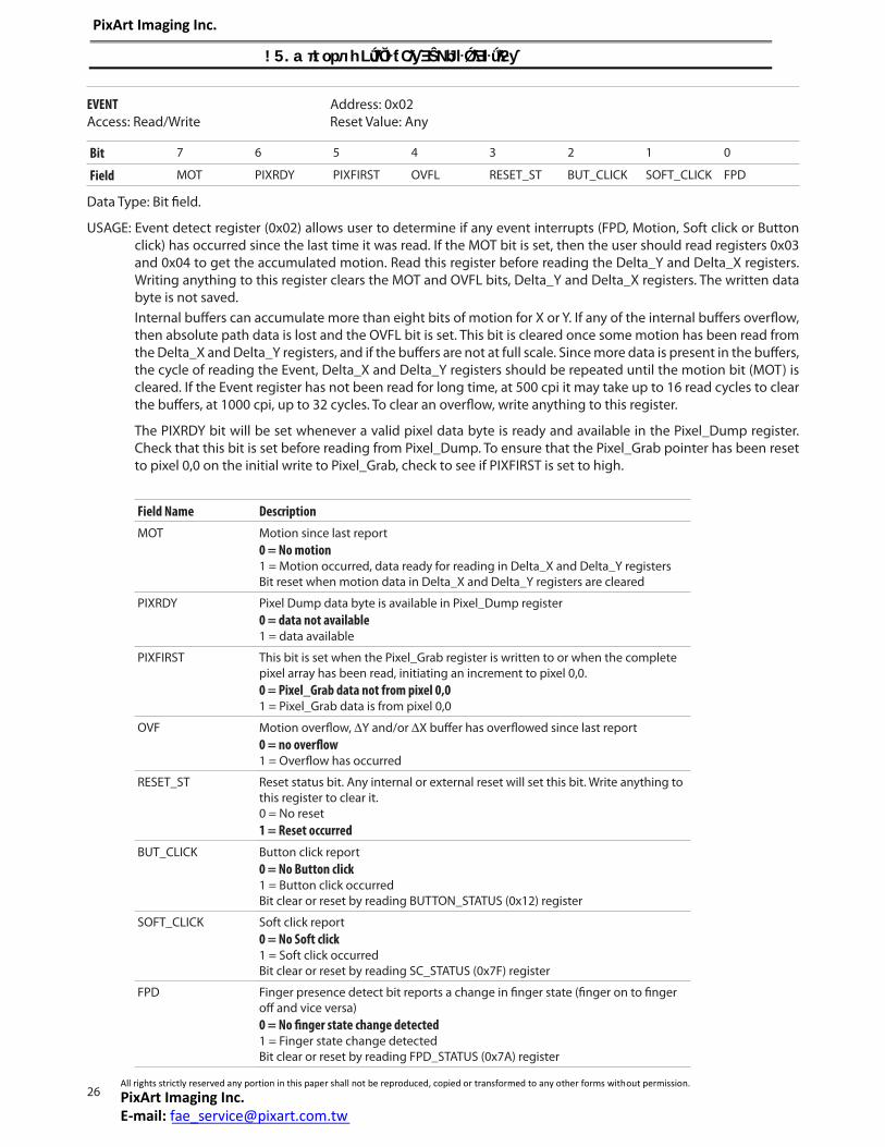
EVENT Address: 0x02 Access: Read/Write Reset Value: Any
Bit 7 6 5 4 3 2 1 0
Field MOT PIXRDY PIXFIRST OVFL RESET_ST BUT_CLICK SOFT_CLICK FPD
Data Type: Bit fi eld.
USAGE: Event detect register (0x02) allows user to determine if any event interrupts (FPD, Motion, Soft click or Button click) has occurred since the last time it was read. If the MOT bit is set, then the user should read registers 0x03 and 0x04 to get the accumulated motion. Read this register before reading the Delta_Y and Delta_X registers. Writing anything to this register clears the MOT and OVFL bits, Delta_Y and Delta_X registers. The written data byte is not saved.
Internal buff ers can accumulate more than eight bits of motion for X or Y. If any of the internal buff ers overfl ow, then absolute path data is lost and the OVFL bit is set. This bit is cleared once some motion has been read from the Delta_X and Delta_Y registers, and if the buff ers are not at full scale. Since more data is present in the buff ers, the cycle of reading the Event, Delta_X and Delta_Y registers should be repeated until the motion bit (MOT) is cleared. If the Event register has not been read for long time, at 500 cpi it may take up to 16 read cycles to clear the buff ers, at 1000 cpi, up to 32 cycles. To clear an overfl ow, write anything to this register.
The PIXRDY bit will be set whenever a valid pixel data byte is ready and available in the Pixel_Dump register. Check that this bit is set before reading from Pixel_Dump. To ensure that the Pixel_Grab pointer has been reset to pixel 0,0 on the initial write to Pixel_Grab, check to see if PIXFIRST is set to high.
Field Name Description
MOT Motion since last report0 = No motion1 = Motion occurred, data ready for reading in Delta_X and Delta_Y registersBit reset when motion data in Delta_X and Delta_Y registers are cleared
PIXRDY Pixel Dump data byte is available in Pixel_Dump register0 = data not available1 = data available
PIXFIRST This bit is set when the Pixel_Grab register is written to or when the complete pixel array has been read, initiating an increment to pixel 0,0.0 = Pixel_Grab data not from pixel 0,01 = Pixel_Grab data is from pixel 0,0
OVF Motion overfl ow, Y and/or X buff er has overfl owed since last report0 = no overfl ow1 = Overfl ow has occurred
RESET_ST Reset status bit. Any internal or external reset will set this bit. Write anything to this register to clear it.0 = No reset1 = Reset occurred
BUT_CLICK Button click report0 = No Button click1 = Button click occurredBit clear or reset by reading BUTTON_STATUS (0x12) register
SOFT_CLICK Soft click report0 = No Soft click 1 = Soft click occurredBit clear or reset by reading SC_STATUS (0x7F) register
FPD Finger presence detect bit reports a change in fi nger state (fi nger on to fi nger off and vice versa)0 = No fi nger state change detected1 = Finger state change detectedBit clear or reset by reading FPD_STATUS (0x7A) register
PixArt Imaging Inc.
!5.aπ!орл hLJǘƛŎŀƭ CƛƴƎŜNJ bŀǾƛƎŀǘƛƻƴ
All rights strictly reserved any portion in this paper shall not be reproduced, copied or transformed to any other forms without permission.
PixArt Imaging Inc. E-mail: [email protected]

27
Delta_X Address: 0x03 Access: Read Reset Value: Any
Bit 7 6 5 4 3 2 1 0
Field Y7 Y6 Y5 Y4 Y3 Y2 Y1 Y0
Data Type: Eight bit 2’s complement number.
USAGE: X movement is counts since last report. Absolute value is determined by resolution. Reading clears the register.
Delta_Y Address: 0x04 Access: Read Reset Value: Any
Bit 7 6 5 4 3 2 1 0
Field X7 X6 X5 X4 X3 X2 X1 X0
Data Type: Eight bit 2’s complement number.
USAGE: Y movement is counts since last report. Absolute value is determined by resolution. Reading clears the register.
00 01 02 7E 7FFFFE81Delta_X
+127+126-1-2-127Motion +1 +20
NOTES: PixArt RECOMMENDS that registers 0x03 and 0x04 be read sequentially.
00 01 02 7E 7FFFFE81Delta_X
+127+126-1-2-127Motion +1 +20
NOTES: PixArt RECOMMENDS that registers 0x03 and 0x04 be read sequentially.
SQUAL Address: 0x05 Access: Read Reset Value: Any
Bit 7 6 5 4 3 2 1 0
Field SQ7 SQ6 SQ5 SQ4 SQ3 SQ2 SQ1 SQ0
Data Type: Upper 8 bits of a 9-bit unsigned integer.
USAGE: SQUAL (Surface Quality) is a measure of the number of valid features visible by the sensor in the current frame. The maximum SQUAL register value is 167. Since small changes in the current frame can result in changes in SQUAL, variations in SQUAL when looking at a surface are expected.
PixArt Imaging Inc.
!5.aπ!орл hLJǘƛŎŀƭ CƛƴƎŜNJ bŀǾƛƎŀǘƛƻƴ
All rights strictly reserved any portion in this paper shall not be reproduced, copied or transformed to any other forms without permission.
PixArt Imaging Inc. E-mail: [email protected]

28
Shutter_Upper Address: 0x06 Access: Read Reset Value: Any
Bit 7 6 5 4 3 2 1 0
Field S15 S14 S13 S12 S11 S10 S9 S8
Shutter_Lower Address: 0x07 Access: Read Reset Value: Undefi ned
Bit 7 6 5 4 3 2 1 0
Field S7 S6 S5 S4 S3 S2 S1 S0
Data Type: Sixteen bit unsigned integer.
USAGE: Units are clock cycles. Read Shutter_Upper fi rst, then Shutter_Lower. They should be read consecutively. The shutter is adjusted to keep the average and maximum pixel values within normal operating ranges. The shutter value is automatically adjusted.
Maximum_Pixel Address: 0x08 Access: Read Reset Value: Any
Bit 7 6 5 4 3 2 1 0
Field MP7 MP6 MP5 MP4 MP3 MP2 MP1 MP0
Data Type: Eight-bit number.
USAGE: Maximum Pixel value in current frame. Minimum value = 0, maximum value = 254. The maximum pixel value can vary with every frame.
Pixel_Sum Address: 0x09 Access: Read Reset Value: Any
Bit 7 6 5 4 3 2 1 0
Field AP7 AP6 AP5 AP4 AP3 AP2 AP1 AP0
Data Type: High 8 bits of an unsigned 17-bit integer.
USAGE: This register is used to fi nd the average pixel value. It reports the seven bits of a 16-bit counter, which sums all pixels in the current frame. It may be described as the full sum divided by 512. To fi nd the average pixel value, use the following formula:
Average Pixel = Register Value * 128/121 = Register Value * 1.06
The maximum register value is 240. The minimum is 0. The pixel sum value can change every frame.
PixArt Imaging Inc.
!5.aπ!орл hLJǘƛŎŀƭ CƛƴƎŜNJ bŀǾƛƎŀǘƛƻƴ
All rights strictly reserved any portion in this paper shall not be reproduced, copied or transformed to any other forms without permission.
PixArt Imaging Inc. E-mail: [email protected]

29
Minimum_Pixel Address: 0x0a Access: Read Reset Value: Any
Bit 7 6 5 4 3 2 1 0
Field MP7 MP6 MP5 MP4 MP3 MP2 MP1 MP0
Data Type: Eight-bit number.
USAGE: Minimum Pixel value in current frame. Minimum value = 0, maximum value = 254. The minimum pixel value can vary with every frame.
Pixel_Grab Address: 0x0b Access: Read/Write Reset Value: Any
Bit 7 6 5 4 3 2 1 0
Field PD7 PD6 PD5 PD4 PD3 PD2 PD1 PD0
Data Type: Eight-bit word.
USAGE: For test purposes, the sensor will read out the contents of the pixel array, one pixel per frame. To start a pixel grab, write anything to this register to reset the pointer to pixel 0,0. Then read the PIXRDY bit in the Motion register. When the PIXRDY bit is set, there is valid data in this register to read out. After the data in this register is read, the pointer will automatically increment to the next pixel. Reading may continue indefi nitely; once a complete frame’s worth of pixels has been read, PIXFIRST will be set to high to indicate the start of the fi rst pixel and the address pointer will start at the beginning location again. The pixel map address and corresponding sensor orientation is shown below.
PixArt Imaging Inc.
!5.aπ!орл hLJǘƛŎŀƭ CƛƴƎŜNJ bŀǾƛƎŀǘƛƻƴ
All rights strictly reserved any portion in this paper shall not be reproduced, copied or transformed to any other forms without permission.
PixArt Imaging Inc. E-mail: [email protected]

30
Figure 23. Top view of pixel map address without lens
0 1 2 3 4 5 6 7 8 9 10 11 12 13 14 15 16 17 18
19 20 21 22 23 24 25 26 27 28 29 30 31 32 33 34 35 36 37
38 39 40 41 42 43 44 45 46 47 48 49 50 51 52 53 54 55 56
57 58 59 60 61 62 63 64 65 66 67 68 69 70 71 72 73 74 75
76 77 78 79 80 81 82 83 84 85 86 87 88 89 90 91 92 93 94
95 96 97 98 99 100 101 102 103 104 105 106 107 108 109 110 111 112 113
114 115 116 117 118 119 120 121 122 123 124 125 126 127 128 129 130 131 132
133 134 135 136 137 138 139 140 141 142 143 144 145 146 147 148 149 150 151
152 153 154 155 156 157 158 159 160 161 162 163 164 165 166 167 168 169 170
171 172 173 174 175 176 177 178 179 180 181 182 183 184 185 186 187 188 189
190 191 192 193 194 195 196 197 198 199 200 201 202 203 204 205 206 207 208
209 210 211 212 213 214 215 216 217 218 219 220 221 222 223 224 225 226 227
228 229 230 231 232 233 234 235 236 237 238 239 240 241 242 243 244 245 246
247 248 249 250 251 252 253 254 255 256 257 258 259 260 261 262 263 264 265
266 267 268 269 270 271 272 273 274 275 276 277 278 279 280 281 282 283 284
285 286 287 288 289 290 291 292 293 294 295 296 297 298 299 300 301 302 303
304 305 306 307 308 309 310 311 312 313 314 315 316 317 318 319 320 321 322
323 324 325 326 327 328 329 330 331 332 333 334 335 336 337 338 339 340 341
342 343 344 345 346 347 348 349 350 351 352 353 354 355 356 357 358 359 360
360 359 358 357 356 355 354 353 352 351 350 349 348 347 346 345 344 343 342
341 340 339 338 337 336 335 334 333 332 331 330 329 328 327 326 325 324 323
322 321 320 319 318 317 316 315 314 313 312 311 310 309 308 307 306 305 304
303 302 301 300 299 298 297 296 295 294 293 292 291 290 289 288 287 286 285
284 283 282 281 280 279 278 277 276 275 274 273 272 271 270 269 268 267 266
265 264 263 262 261 260 259 258 257 256 255 254 253 252 251 250 249 248 247
246 245 244 243 242 241 240 239 238 237 236 235 234 233 232 231 230 229 228
227 226 225 224 223 222 221 220 219 218 217 216 215 214 213 212 211 210 209
208 207 206 205 204 203 202 201 200 199 198 197 196 195 194 193 192 191 190
189 188 187 186 185 184 183 182 181 180 179 178 177 176 175 174 173 172 171
170 169 168 167 166 165 164 163 162 161 160 159 158 157 156 155 154 153 152
151 150 149 148 147 146 145 144 143 142 141 140 139 138 137 136 135 134 133
132 131 130 129 128 127 126 125 124 123 122 121 120 119 118 117 116 115 114
113 112 111 110 109 108 107 106 105 104 103 102 101 100 99 98 97 96 95
94 93 92 91 90 89 88 87 86 85 84 83 82 81 80 79 78 77 76
75 74 73 72 71 70 69 68 67 66 65 64 63 62 61 60 59 58 57
56 55 54 53 52 51 50 49 48 47 46 45 44 43 42 41 40 39 38
37 36 35 34 33 32 31 30 29 28 27 26 25 24 23 22 21 20 19
18 17 16 15 14 13 12 11 10 9 8 7 6 5 4 3 2 1 0
Figure 24. Top view of pixel map address with lens
PixArt Imaging Inc.
!5.aπ!орл hLJǘƛŎŀƭ CƛƴƎŜNJ bŀǾƛƎŀǘƛƻƴ
All rights strictly reserved any portion in this paper shall not be reproduced, copied or transformed to any other forms without permission.
PixArt Imaging Inc. E-mail: [email protected]

31
CRC2 Address: 0x0e Access: Read Reset Value: 0x00
Bit 7 6 5 4 3 2 1 0
Field CRC27 CRC26 CRC25 CRC24 CRC23 CRC22 CRC21 CRC20
Data Type: Eight-bit number
USAGE: Register 0x0e reports the third byte of the system self test results. See Self Test register 0x10.
CRC3 Address: 0x0f Access: Read Reset Value: 0x00
Bit 7 6 5 4 3 2 1 0
Field CRC37 CRC36 CRC35 CRC34 CRC33 CRC32 CRC31 CRC30
Data Type: Eight-bit number
USAGE: Register 0x0f reports the fourth byte of the system self test results. See Self Test register 0x10.
CRC0 Address: 0x0c Access: Read Reset Value: 0x00
Bit 7 6 5 4 3 2 1 0
Field CRC07 CRC06 CRC05 CRC04 CRC03 CRC02 CRC01 CRC00
Data Type: Eight-bit number
USAGE: Register 0x0c reports the fi rst byte of the system self test results. See Self Test register 0x10.
CRC1 Address: 0x0d Access: Read Reset Value: 0x00
Bit 7 6 5 4 3 2 1 0
Field CRC17 CRC16 CRC15 CRC14 CRC13 CRC12 CRC11 CRC10
Data Type: Eight-bit number
USAGE: Register 0x0d reports the second byte of the system self test results. See Self Test register 0x10.
PixArt Imaging Inc.
!5.aπ!орл hLJǘƛŎŀƭ CƛƴƎŜNJ bŀǾƛƎŀǘƛƻƴ
All rights strictly reserved any portion in this paper shall not be reproduced, copied or transformed to any other forms without permission.
PixArt Imaging Inc. E-mail: [email protected]
Self_Test Address: Access: Write Reset Value:

33
Run_Downshift Address: 0x13 Access: Read/Write Reset Value: 0x04
Bit 7 6 5 4 3 2 1 0
Field RD7 RD6 RD5 RD4 RD3 RD2 RD1 RD0
This register set the Run to Rest 1 downshift time.
Run Downshift time = RD[7:0] x 8 x Run_rate.
Default value: 4 x 8 x 8 ms = 256 msMin: 2 x 8 x 8 ms = 128 msMax: 242 x 8 x 8 ms = 15,488 ms = 15.49 s
All the above values are calculated base on 25 MHz System clock.
Rest1_Period Address: 0x14 Access: Read/Write Reset Value: 0x01
Bit 7 6 5 4 3 2 1 0
Field R1R7 R1R6 R1R5 R1R4 R1R3 R1R2 R1R1 R1R0
This register set the Rest 1 frame rate.
Rest1 frame rate = (R1R[7:0] + 1) x 10 ms.
Default value: 2 x 10 ms = 20 msMin: 2 x 10 ms = 20 msMax: 241 x 10 ms = 2,410 ms = 2.41 s
All the above values are calculated base on 100 Hz Hibernate clock.
BUTTON_STATUS Address: 0x12 Access: Read/Write Reset Value: 0x00
Bit 7 6 5 4 3 2 1 0
Field Assert count
Assert count
Deassert count
Deassert count
Reserved Reserved Reserved But_Status
Data Type: Bit fi eld
USAGE: Register 0x12 allows the user to read button status. Writing any value to this register will restart the counter.
Field Name Description
Assert count 7:6 Counts for number of times the button state change from 0 to 1
Deassert count 5:4 Counts for number of times the button state change from 1 to 0
But_Status Button current status
PixArt Imaging Inc.
!5.aπ!орл hLJǘƛŎŀƭ CƛƴƎŜNJ bŀǾƛƎŀǘƛƻƴ
All rights strictly reserved any portion in this paper shall not be reproduced, copied or transformed to any other forms without permission.
PixArt Imaging Inc. E-mail: [email protected]
34
Rest2_Period Address: 0x16 Access: Read/Write Reset Value: 0x09
Bit 7 6 5 4 3 2 1 0
Field R2R7 R2R6 R2R5 R2R4 R2R3 R2R2 R2R1 R2R0
This register set the Rest 2 frame rate.
Rest2 frame rate = (R2R[7:0] + 1) x 10 ms.
Default value: 10 x 10 ms = 100 msMin: 2 x 10 ms = 20 msMax: 241 x 10 ms = 2,410 ms = 2.41 s
All the above values are calculated base on 100 Hz Hibernate clock.
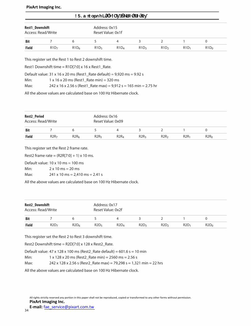
Rest2_Downshift Address: 0x17 Access: Read/Write Reset Value: 0x2f
Bit 7 6 5 4 3 2 1 0
Field R2D7 R2D6 R2D5 R2D4 R2D3 R2D2 R2D1 R2D0
This register set the Rest 2 to Rest 3 downshift time.
Rest2 Downshift time = R2D[7:0] x 128 x Rest2_Rate.
Default value: 47 x 128 x 100 ms (Rest2_Rate default) = 601.6 s = 10 minMin: 1 x 128 x 20 ms (Rest2_Rate min) = 2560 ms = 2.56 sMax: 242 x 128 x 2.56 s (Resr2_Rate max) = 79,298 s = 1,321 min = 22 hrs
All the above values are calculated base on 100 Hz Hibernate clock.
Rest1_Downshift Address: 0x15 Access: Read/Write Reset Value: 0x1f
Bit 7 6 5 4 3 2 1 0
Field R1D7 R1D6 R1D5 R1D4 R1D3 R1D2 R1D1 R1D0
This register set the Rest 1 to Rest 2 downshift time.
Rest1 Downshift time = R1D[7:0] x 16 x Rest1_Rate.
Default value: 31 x 16 x 20 ms (Rest1_Rate default) = 9,920 ms = 9.92 sMin: 1 x 16 x 20 ms (Rest1_Rate min) = 320 msMax: 242 x 16 x 2.56 s (Rest1_Rate max) = 9,912 s = 165 min = 2.75 hr
All the above values are calculated base on 100 Hz Hibernate clock.
PixArt Imaging Inc.
!5.aπ!орл hLJǘƛŎŀƭ CƛƴƎŜNJ bŀǾƛƎŀǘƛƻƴ
All rights strictly reserved any portion in this paper shall not be reproduced, copied or transformed to any other forms without permission.
PixArt Imaging Inc. E-mail: [email protected]

35
Reserved Address: 0x19
LED_Control Address: 0x1a Access: Read/Write Reset Value: 0x00
Bit 7 6 5 4 3 2 1 0
Field Reserved Reserved Reserved Reserved LED_On LED2 LED1 LED0
Data Type: Bit fi eld
USAGE: Register 0x1a allows the user to change the LED drive current of the sensor.
Field Name Description
LED_On 0 = LED normal operation1 = LED always On
LED2:0 0x00 = 13 mA0x02 = 9.6 mA0x07 = 27 mA
Reserved Address: 0x1b
Rest3_Period Address: 0x18 Access: Read/Write Reset Value: 0x31
Bit 7 6 5 4 3 2 1 0
Field R3R7 R3R6 R3R5 R3R4 R3R3 R3R2 R3R1 R3R0
This register set the Rest 3 frame rate.
Rest3 frame rate = (R3R[7:0] + 1) x 10 ms.
Default value: 50 x 10 ms = 500 msMin: 2 x 10 ms = 20 msMax: 241 x 10 ms = 2,410 ms = 2.41 s
All the above values are calculated base on 100 Hz Hibernate clock.
PixArt Imaging Inc.
!5.aπ!орл hLJǘƛŎŀƭ CƛƴƎŜNJ bŀǾƛƎŀǘƛƻƴ
All rights strictly reserved any portion in this paper shall not be reproduced, copied or transformed to any other forms without permission.
PixArt Imaging Inc. E-mail: [email protected]
36
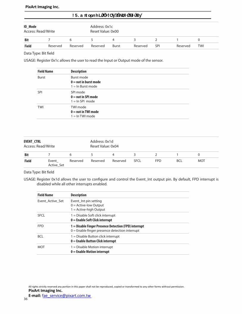
EVENT_CTRL Address: 0x1d Access: Read/Write Reset Value: 0x04
Bit 7 6 5 4 3 2 1 0
Field Event_Active_Set
Reserved Reserved Reserved SFCL FPD BCL MOT
Data Type: Bit fi eld
USAGE: Register 0x1d allows the user to confi gure and control the Event_Int output pin. By default, FPD interrupt is disabled while all other interrupts enabled.
Field Name Description
Event_Active_Set Event_Int pin setting0 = Active-low Output1 = Active-high Output
SFCL 1 = Disable Soft click interrupt 0 = Enable Soft Click interrupt
FPD 1 = Disable Finger Presence Detection (FPD) interrupt 0 = Enable fi nger presence detection interrupt
BCL 1 = Disable Button click interrupt 0 = Enable Button Click interrupt
MOT 1 = Disable Motion interrupt 0 = Enable Motion interrupt
IO_Mode Address: 0x1c Access: Read/Write Reset Value: 0x00
Bit 7 6 5 4 3 2 1 0
Field Reserved Reserved Reserved Burst Reserved SPI Reserved TWI
Data Type: Bit fi eld
USAGE: Register 0x1c allows the user to read the Input or Output mode of the sensor.
Field Name Description
Burst Burst mode0 = not in burst mode1 = In Burst mode
SPI SPI mode0 = not in SPI mode1 = In SPI mode
TWI TWI mode0 = not in TWI mode1 = In TWI mode
PixArt Imaging Inc.
!5.aπ!орл hLJǘƛŎŀƭ CƛƴƎŜNJ bŀǾƛƎŀǘƛƻƴ
All rights strictly reserved any portion in this paper shall not be reproduced, copied or transformed to any other forms without permission.
PixArt Imaging Inc. E-mail: [email protected]

37
Observation Address: 0x2e Access: Read/Write Reset Value: Any
Bit 7 6 5 4 3 2 1 0
Field MODE1 MODE0 Reserved Reserved Reserved Reserved Reserved Reserved
Data Type: Bit fi eld
USAGE: Register 0x2e provides bits that are set every frame. It can be used during ESD testing to check that the chip is running correctly. Writing anything to this register will clear the bits.
Field Name Description
MODE1-0 Mode Status: Reports which mode the sensor is in.00 = Run01 = Rest110 = Rest211 = Rest3
Address: 0x28 Access: Read/Write Reset Value: 0x00
Bit 7 6 5 4 3 2 1 0
Field Reserved Reserved Reserved Reserved Reserved Reserved Reserved FVD
Data Type: Bit fi eld
USAGE: This register is used to enable and initiating Fast Dump. See note on Dump for more information.
Field Name Description
FVD 0: Disable FVD1: Enable FVD
PixArt Imaging Inc.
!5.aπ!орл hLJǘƛŎŀƭ CƛƴƎŜNJ bŀǾƛƎŀǘƛƻƴ
All rights strictly reserved any portion in this paper shall not be reproduced, copied or transformed to any other forms without permission.
PixArt Imaging Inc. E-mail: [email protected]
38
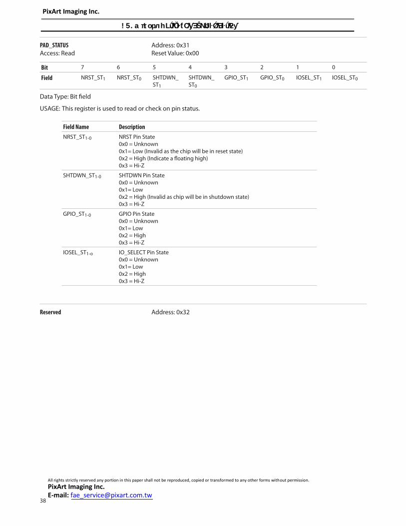
PAD_STATUS Address: 0x31 Access: Read Reset Value: 0x00
Bit 7 6 5 4 3 2 1 0
Field NRST_ST1 NRST_ST0 SHTDWN_ST1
SHTDWN_ST0
GPIO_ST1 GPIO_ST0 IOSEL_ST1 IOSEL_ST0
Data Type: Bit fi eld
USAGE: This register is used to read or check on pin status.
Field Name Description
NRST_ST1-0 NRST Pin State 0x0 = Unknown0x1= Low (Invalid as the chip will be in reset state)0x2 = High (Indicate a fl oating high)0x3 = Hi-Z
SHTDWN_ST1-0 SHTDWN Pin State0x0 = Unknown0x1= Low 0x2 = High (Invalid as chip will be in shutdown state)0x3 = Hi-Z
GPIO_ST1-0 GPIO Pin State0x0 = Unknown0x1= Low 0x2 = High 0x3 = Hi-Z
IOSEL_ST1-o IO_SELECT Pin State0x0 = Unknown0x1= Low 0x2 = High 0x3 = Hi-Z
Reserved Address: 0x32
PixArt Imaging Inc.
!5.aπ!орл hLJǘƛŎŀƭ CƛƴƎŜNJ bŀǾƛƎŀǘƛƻƴ
All rights strictly reserved any portion in this paper shall not be reproduced, copied or transformed to any other forms without permission.
PixArt Imaging Inc. E-mail: [email protected]

39
SOFT_RESET Address: 0x3a Access: Write Reset Value: 0x00
Bit 7 6 5 4 3 2 1 0
Field RST7 RST6 RST5 RST4 RST3 RST2 RST1 RST0
Data Type: 8-bit integer
USAGE: Write 0x5A to this register to reset the chip. All settings will revert to default values.
PAD_TEST_OUT Address: 0x33 Access: Read/Write Reset Value: 0x00
Bit 7 6 5 4 3 2 1 0
Field Reserved Reserved Reserved Reserved EVENT_O GPIO_O MOSI_O MISO_O
Data Type: Bit fi eld
USAGE: This register is used to set the state of the output pin.
Field Name Description
EVENT_O Set state for EVENT_INT output pin 0x0: Low0x1: High
GPIO_O Set state for GPIO_O output pin 0x0: Low0x1: High
MOSI_O Set state for MOSI_O output pin 0x0: Low0x1: High
MISO_O Set state for MISO_O output pin 0x0: Low0x1: High
PAD_FUNCTION Address: 0x34 Access: Write Reset Value: 0x00
Bit 7 6 5 4 3 2 1 0
Field Reserved Reserved Reserved OUT_TEST_EN
Reserved Reserved Reserved Reserved
Data Type: Bit fi eld
USAGE: This register is used to enable output pin testing.
Field Name Description
OUT_TEST_EN Enable Output Pin Test
All rights strictly reserved any portion in this paper shall not be reproduced, copied or transformed to any other forms without permission.
PixArt Imaging Inc. E-mail: [email protected]
PixArt Imaging Inc.
!5.aπ!орл hLJǘƛŎŀƭ CƛƴƎŜNJ bŀǾƛƎŀǘƛƻƴ

40
Shutter_Max_Hi Address: 0x3b Access: Read/Write Reset Value: 0x0b
Bit 7 6 5 4 3 2 1 0
Field SMH7 SMH6 SMH5 SMH4 SMH3 SMH2 SMH1 SMH0
Data Type: 8-Bit integer
USAGE: This value is the upper 8-bit of shutter maximum open time. Shutter value represents pixel array exposure time in multiples of internal clock cycles with maximum value at 2929 decimal.
Shutter_Max_Lo Address: 0x3c Access: Read/Write Reset Value: 0x71
Bit 7 6 5 4 3 2 1 0
Field SML7 SML6 SML5 SML4 SML3 SML2 SML1 SML0
Data Type: 8-Bit integer
USAGE: This value is the lower 8-bit of shutter maximum open time. Shutter value represents pixel array exposure time in multiples of internal clock cycles.
Reserved Address: 0x3d
Inverse_Revision_ID Address: 0x3e Access: Read Reset Value: 0xFF
Bit 7 6 5 4 3 2 1 0
Field NRID7 NRID6 NRID5 NRID4 NRID3 NRID2 NRID1 NRID0
Data Type: Inverse 8-Bit unsigned integer
USAGE: This value is the inverse of the Revision_ID. It can be used to test the SPI port.
Inverse_Product_ID Address: 0x3f Access: Read Reset Value: 0x77
Bit 7 6 5 4 3 2 1 0
Field NPID7 NPID6 NPID5 NPID4 NPID3 NPID2 NPID1 NPID0
Data Type: Inverse 8-Bit unsigned integer
USAGE: This value is the inverse of the Product_ID. It can be used to test the SPI port.
All rights strictly reserved any portion in this paper shall not be reproduced, copied or transformed to any other forms without permission.
PixArt Imaging Inc. E-mail: [email protected]
PixArt Imaging Inc.
!5.aπ!орл hLJǘƛŎŀƭ CƛƴƎŜNJ bŀǾƛƎŀǘƛƻƴ
41
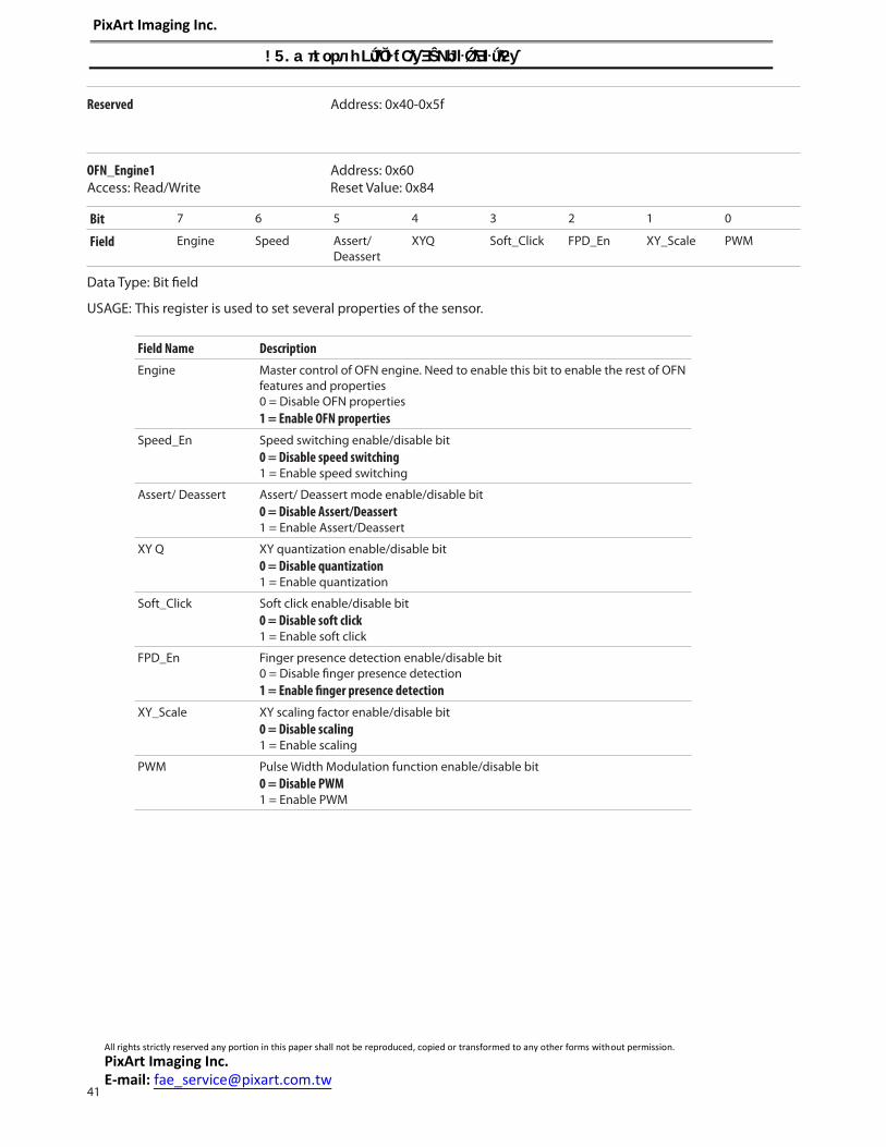
Reserved Address: 0x40-0x5f
OFN_Engine1 Address: 0x60 Access: Read/Write Reset Value: 0x84
Bit 7 6 5 4 3 2 1 0
Field Engine Speed Assert/Deassert
XYQ Soft_Click FPD_En XY_Scale PWM
Data Type: Bit fi eld
USAGE: This register is used to set several properties of the sensor.
Field Name Description
Engine Master control of OFN engine. Need to enable this bit to enable the rest of OFN features and properties0 = Disable OFN properties1 = Enable OFN properties
Speed_En Speed switching enable/disable bit0 = Disable speed switching1 = Enable speed switching
Assert/ Deassert Assert/ Deassert mode enable/disable bit0 = Disable Assert/Deassert1 = Enable Assert/Deassert
XY Q XY quantization enable/disable bit0 = Disable quantization1 = Enable quantization
Soft_Click Soft click enable/disable bit0 = Disable soft click1 = Enable soft click
FPD_En Finger presence detection enable/disable bit0 = Disable fi nger presence detection1 = Enable fi nger presence detection
XY_Scale XY scaling factor enable/disable bit0 = Disable scaling1 = Enable scaling
PWM Pulse Width Modulation function enable/disable bit0 = Disable PWM1 = Enable PWM
All rights strictly reserved any portion in this paper shall not be reproduced, copied or transformed to any other forms without permission.
PixArt Imaging Inc. E-mail: [email protected]
PixArt Imaging Inc.
!5.aπ!орл hLJǘƛŎŀƭ CƛƴƎŜNJ bŀǾƛƎŀǘƛƻƴ

42
Resolution Address: 0x62 Access: Read/Write Reset Value: 0x32
Bit 7 6 5 4 3 2 1 0
Field WakeRES3 WakeRES2 WakeRES1 WakeRES0 RES3 RES2 RES1 RES0
Data Type: Bit fi eld
USAGE: This register is used to set several properties of the sensor.
Field Name Description
WakeRES3:0 Sets resolution when sensor wakes up from rest modes. Eff ective only when speed switching is enabled.0x00 : 125 cpi 0x05 : 1250 cpi0x01 : 250 cpi 0x02 : 500 cpi 0x03 : 750 cpi 0x04 : 1000 cpi
RES3:0 Sets resolution of sensor.0x00 : 125 cpi 0x05 : 1250 cpi0x01 : 250 cpi 0x02 : 500 cpi 0x03 : 750 cpi 0x04 : 1000 cpi
If Speed switching is enabled, resolution is automatically switched from 250-500-750-1000-1250.If speed switching is disabled, this register can be set to any of the available settings from 0x0 to 0x5.
OFN_Engine2 Address: 0x61 Access: Read/Write Reset Value: 0x89
Bit 7 6 5 4 3 2 1 0
Field Reserved Reserved FPD_Rest_Wake1
FPD_Rest_Wake0
FPD_Mot_Cut
Reserved PAD_Chk On FPD_SQ_EN
Data Type: Bit fi eld
USAGE: This register is used to set several properties of the sensor related to FPD function.
Field Name Description
FPD_Rest_Wake1:0 Wakes up from rest with FPD0 = FPD rest wake up disabled1 = Wake up when fi nger is present OR motion is detected2 = Wake up when fi nger is present AND motion is detected
FPD_Mot_Cut In FPD enabled mode, cut off motion when fi nger is not detected and shutter is below preset value.Shutter preset value can confi gured by SHUT_CUTOFF_THRES in FPD_CTRL (register 0x75).0 = Disable FPD_Mot_Cut1 = Enable FPD_Mot_Cut
PAD_Chk_On Enable this bit for PAD_STATUS check
FPD_SQ_EN To improve FPD on low refl ectance surface by comparing the instantaneous Squal value with a threshold set in FPD_SQUAL_THRESH (register 0x78).0 = Disable FPD_SQ_EN 1 = Enable FPD_SQ_EN
All rights strictly reserved any portion in this paper shall not be reproduced, copied or transformed to any other forms without permission.
PixArt Imaging Inc. E-mail: [email protected]
PixArt Imaging Inc.
!5.aπ!орл hLJǘƛŎŀƭ CƛƴƎŜNJ bŀǾƛƎŀǘƛƻƴ
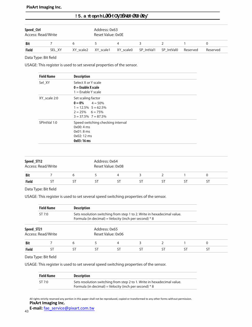
43
Speed_Ctrl Address: 0x63 Access: Read/Write Reset Value: 0x0E
Bit 7 6 5 4 3 2 1 0
Field SEL_XY XY_scale2 XY_scale1 XY_scale0 SP_IntVal1 SP_IntVal0 Reserved Reserved
Data Type: Bit fi eld
USAGE: This register is used to set several properties of the sensor.
Field Name Description
Sel_XY Select X or Y scale0 = Enable X scale1 = Enable Y scale
XY_scale 2:0 Set scaling factor0 = 0% 4 = 50%1 = 12.5% 5 = 62.5%2 = 25% 6 = 75%3 = 37.5% 7 = 87.5%
SPIntVal 1:0 Speed switching checking interval0x00: 4 ms0x01: 8 ms 0x02: 12 ms0x03: 16 ms
Speed_ST12 Address: 0x64 Access: Read/Write Reset Value: 0x08
Bit 7 6 5 4 3 2 1 0
Field ST ST ST ST ST ST ST ST
Data Type: Bit fi eld
USAGE: This register is used to set several speed switching properties of the sensor.
Field Name Description
ST 7:0 Sets resolution switching from step 1 to 2. Write in hexadecimal value.Formula (in decimal) = Velocity (inch per second) * 8
Speed_ST21 Address: 0x65 Access: Read/Write Reset Value: 0x06
Bit 7 6 5 4 3 2 1 0
Field ST ST ST ST ST ST ST ST
Data Type: Bit fi eld
USAGE: This register is used to set several speed switching properties of the sensor.
Field Name Description
ST 7:0 Sets resolution switching from step 2 to 1. Write in hexadecimal value.Formula (in decimal) = Velocity (inch per second) * 8
All rights strictly reserved any portion in this paper shall not be reproduced, copied or transformed to any other forms without permission.
PixArt Imaging Inc. E-mail: [email protected]
PixArt Imaging Inc.
!5.aπ!орл hLJǘƛŎŀƭ CƛƴƎŜNJ bŀǾƛƎŀǘƛƻƴ
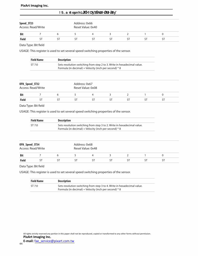
44
Speed_ST23 Address: 0x66 Access: Read/Write Reset Value: 0x40
Bit 7 6 5 4 3 2 1 0
Field ST ST ST ST ST ST ST ST
Data Type: Bit fi eld
USAGE: This register is used to set several speed switching properties of the sensor.
Field Name Description
ST 7:0 Sets resolution switching from step 2 to 3. Write in hexadecimal value.Formula (in decimal) = Velocity (inch per second) * 8
OFN_Speed_ST32 Address: 0x67 Access: Read/Write Reset Value: 0x08
Bit 7 6 5 4 3 2 1 0
Field ST ST ST ST ST ST ST ST
Data Type: Bit fi eld
USAGE: This register is used to set several speed switching properties of the sensor.
Field Name Description
ST 7:0 Sets resolution switching from step 3 to 2. Write in hexadecimal value.Formula (in decimal) = Velocity (inch per second) * 8
OFN_Speed_ST34 Address: 0x68 Access: Read/Write Reset Value: 0x48
Bit 7 6 5 4 3 2 1 0
Field ST ST ST ST ST ST ST ST
Data Type: Bit fi eld
USAGE: This register is used to set several speed switching properties of the sensor.
Field Name Description
ST 7:0 Sets resolution switching from step 3 to 4. Write in hexadecimal value.Formula (in decimal) = Velocity (inch per second) * 8
All rights strictly reserved any portion in this paper shall not be reproduced, copied or transformed to any other forms without permission.
PixArt Imaging Inc. E-mail: [email protected]
PixArt Imaging Inc.
!5.aπ!орл hLJǘƛŎŀƭ CƛƴƎŜNJ bŀǾƛƎŀǘƛƻƴ

45
Speed_ST45 Address: 0x6a Access: Read/Write Reset Value: 0x50
Bit 7 6 5 4 3 2 1 0
Field ST ST ST ST ST ST ST ST
Data Type: Bit fi eld
USAGE: This register is used to set several speed switching properties of the sensor.
Field Name Description
ST 7:0 Sets resolution switching from step 4 to 5. Write in hexadecimal value.Formula (in decimal) = Velocity (inch per second) * 8
Speed_ST43 Address: 0x69 Access: Read/Write Reset Value: 0x0a
Bit 7 6 5 4 3 2 1 0
Field ST ST ST ST ST ST ST ST
Data Type: Bit fi eld
USAGE: This register is used to set several speed switching properties of the sensor.
Field Name Description
ST 7:0 Sets resolution switching from step 4 to 3. Write in hexadecimal value.Formula (in decimal) = Velocity (inch per second) * 8
Speed_ST54 Address: 0x6b Access: Read/Write Reset Value: 0x48
Bit 7 6 5 4 3 2 1 0
Field ST ST ST ST ST ST ST ST
Data Type: Bit fi eld
USAGE: This register is used to set several speed switching properties of the sensor.
Field Name Description
ST 7:0 Sets resolution switching from step 5 to 4. Write in hexadecimal value.Formula (in decimal) = Velocity (inch per second) * 8
All rights strictly reserved any portion in this paper shall not be reproduced, copied or transformed to any other forms without permission.
PixArt Imaging Inc. E-mail: [email protected]
PixArt Imaging Inc.
!5.aπ!орл hLJǘƛŎŀƭ CƛƴƎŜNJ bŀǾƛƎŀǘƛƻƴ

46
AD_CTRL Address: 0x6d Access: Read/Write Reset Value: 0xc4
Bit 7 6 5 4 3 2 1 0
Field 1 1 Reserved Reserved ST_HIGH3 ST_HIGH2 ST_HIGH1 ST_HIGH0
Data Type: Bit fi eld
USAGE: This register is used to control Assert De-assert. Must write 1to bit 7 and 6.
Field Name Description
ST_HIGH3:0 High speed defi nition.Any steps equal to or above this setting will use high speed A/D threshold.
GPIO_CTRL Address: 0x6c Access: Read/Write Reset Value: 0x80
Bit 7 6 5 4 3 2 1 0
Field GPIO_Active_Set
Reserved GPIO_Mode5
GPIO_Mode4
PWM_Thres3
PWM_Thres2
PWM_Sel1 PWM_Sel0
Data Type: Bit fi eld
USAGE: This register is used to set GPIO and PWM control.
Field Name Description
GPIO_Active_Set 0 = GPIO is active LOW output1 = GPIO is active HIGH output
GPIO_Mode5:4 0 = Output FPD 1 = Output PWM 2 = Mechanical button input
PWM_Thres3:2 Start PWM only when Delta_X + Delta_Y is greater than threshold in Speed mode (Speed bit below). 0 = delta > 0 1 = delta > 8 2 = delta > 16 3 = delta >24
PWM_Sel1:0 0 = Finger On/Off , light up in 1 sec 1 = Finger On/Off , light up in 2 sec2 = Finger On/Off , light up in 3 sec3 = Speed
All rights strictly reserved any portion in this paper shall not be reproduced, copied or transformed to any other forms without permission.
PixArt Imaging Inc. E-mail: [email protected]
PixArt Imaging Inc.
!5.aπ!орл hLJǘƛŎŀƭ CƛƴƎŜNJ bŀǾƛƎŀǘƛƻƴ

47
AD_ATH_HIGH Address: 0x6e Access: Read/Write Reset Value: 0x3a
Bit 7 6 5 4 3 2 1 0
Field ATH_H ATH_H ATH_H ATH_H ATH_H ATH_H ATH_H ATH_H
Data Type: Bit fi eld
USAGE: This register is used to set HIGH speed Assert shutter threshold.
Field Name Description
ATH_H 7:0 Sets HIGH speed assert threshold. Write in hexadecimal value.Formula (in decimal) = Shutter value / 8.It is recommended to have hysteresis of 60 to 100 between assert and de-assert threshold.
AD_DTH_HIGH Address: 0x6f Access: Read/Write Reset Value: 0x40
Bit 7 6 5 4 3 2 1 0
Field DTH_H DTH_H DTH_H DTH_H DTH_H DTH_H DTH_H DTH_H
Data Type: Bit fi eld
USAGE: This register is used to set HIGH speed De-assert shutter threshold.
Field Name Description
DTH_H 7:0 Sets HIGH speed de-assert threshold. Write in hexadecimal value.Formula (in decimal) = Shutter value / 8.It is recommended to have hysteresis of 60 to 100 between assert and de-assert threshold.
AD_ATH_LOW Address: 0x70 Access: Read/Write Reset Value: 0x35
Bit 7 6 5 4 3 2 1 0
Field ATH_L ATH_L ATH_L ATH_L ATH_L ATH_L ATH_L ATH_L
Data Type: Bit fi eld
USAGE: This register is used to set LOW speed Assert shutter threshold.
Field Name Description
ATH_L 7:0 Sets LOW speed assert threshold. Write in hexadecimal value.Formula (in decimal) = Shutter value / 8.It is recommended to have hysteresis of 60 to 100 between assert and de-assert threshold.
All rights strictly reserved any portion in this paper shall not be reproduced, copied or transformed to any other forms without permission.
PixArt Imaging Inc. E-mail: [email protected]
PixArt Imaging Inc.
!5.aπ!орл hLJǘƛŎŀƭ CƛƴƎŜNJ bŀǾƛƎŀǘƛƻƴ

48
AD_DTH_LOW Address: 0x71 Access: Read/Write Reset Value: 0x3b
Bit 7 6 5 4 3 2 1 0
Field DTH_L DTH_L DTH_L DTH_L DTH_L DTH_L DTH_L DTH_L
Data Type: Bit fi eld
USAGE: This register is used to set LOW speed De-assert shutter threshold.
Field Name Description
DTH_L 7:0 Sets LOW speed de-assert threshold. Write in hexadecimal value.Formula (in decimal) = Shutter value / 8.It is recommended to have hysteresis of 60 to 100 between assert and de-assert threshold.
QUANTIZE_CTRL Address: 0x72 Access: Read/Write Reset Value: 0x99
Bit 7 6 5 4 3 2 1 0
Field YQ_ON YQ_DIV6 YQ_DIV5 YQ_DIV4 XQ_ON XQ_DIV2 XQ_DIV1 XQ_DIV0
Data Type: Bit fi eld
USAGE: This register is used to set quatization for Delta_X and Delta_Y. If both X and Y quantization modes are on, then only largest quantized X or Y will be reported.
Field Name Description
YQ_ON 0 = Y quantization off 1 = Y quantization On
YQ_DIV6:4 Quantization factor 2YQ_DIV . Reported YQ = DY / 2YQ_DIV .
XQ_ON 0 = X quantization off 1 = X quantization On
XQ_DIV2:0 Quantization factor 2XQ_DIV . Reported XQ = DX / 2XQ_DIV .
XYQ_THRESH Address: 0x73 Access: Read/Write Reset Value: 0x02
Bit 7 6 5 4 3 2 1 0
Field Reserved Reserved Reserved Reserved Reserved XYQ_M XYQ_C1 XYQ_C0
Data Type: Bit fi eld
USAGE: This register is used to set quatization gradient for DeltaX and DeltaY.
Field Name Description
XYQ_M Gradient of linear region0 = Gradient 11 = Gradient 2
XYQ_C1:0 Indicates the off set of linear region (max of C = 3 or 0x03)
All rights strictly reserved any portion in this paper shall not be reproduced, copied or transformed to any other forms without permission.
PixArt Imaging Inc. E-mail: [email protected]
PixArt Imaging Inc.
!5.aπ!орл hLJǘƛŎŀƭ CƛƴƎŜNJ bŀǾƛƎŀǘƛƻƴ
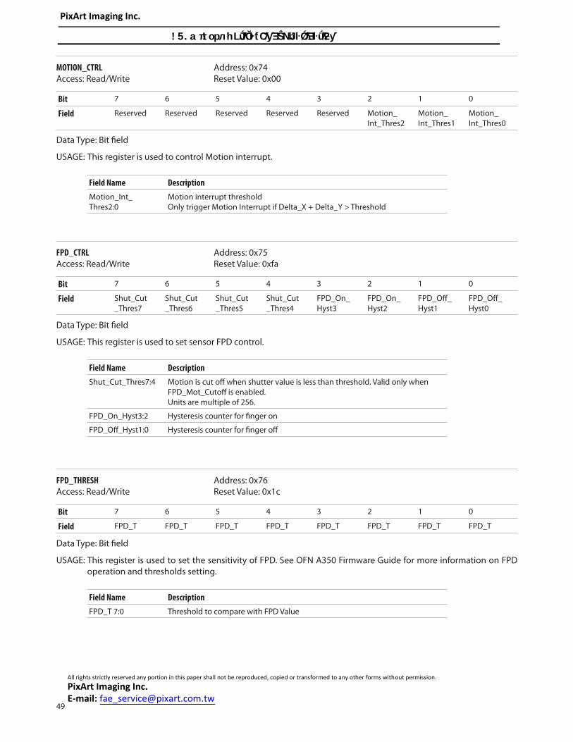
49
MOTION_CTRL Address: 0x74 Access: Read/Write Reset Value: 0x00
Bit 7 6 5 4 3 2 1 0
Field Reserved Reserved Reserved Reserved Reserved Motion_Int_Thres2
Motion_Int_Thres1
Motion_Int_Thres0
Data Type: Bit fi eld
USAGE: This register is used to control Motion interrupt.
Field Name Description
Motion_Int_Thres2:0
Motion interrupt thresholdOnly trigger Motion Interrupt if Delta_X + Delta_Y > Threshold
FPD_CTRL Address: 0x75 Access: Read/Write Reset Value: 0xfa
Bit 7 6 5 4 3 2 1 0
Field Shut_Cut_Thres7
Shut_Cut_Thres6
Shut_Cut_Thres5
Shut_Cut_Thres4
FPD_On_Hyst3
FPD_On_Hyst2
FPD_Off _Hyst1
FPD_Off _Hyst0
Data Type: Bit fi eld
USAGE: This register is used to set sensor FPD control.
Field Name Description
Shut_Cut_Thres7:4 Motion is cut off when shutter value is less than threshold. Valid only when FPD_Mot_Cutoff is enabled.Units are multiple of 256.
FPD_On_Hyst3:2 Hysteresis counter for fi nger on
FPD_Off _Hyst1:0 Hysteresis counter for fi nger off
FPD_THRESH Address: 0x76 Access: Read/Write Reset Value: 0x1c
Bit 7 6 5 4 3 2 1 0
Field FPD_T FPD_T FPD_T FPD_T FPD_T FPD_T FPD_T FPD_T
Data Type: Bit fi eld
USAGE: This register is used to set the sensitivity of FPD. See OFN A350 Firmware Guide for more information on FPD operation and thresholds setting.
Field Name Description
FPD_T 7:0 Threshold to compare with FPD Value
All rights strictly reserved any portion in this paper shall not be reproduced, copied or transformed to any other forms without permission.
PixArt Imaging Inc. E-mail: [email protected]
PixArt Imaging Inc.
!5.aπ!орл hLJǘƛŎŀƭ CƛƴƎŜNJ bŀǾƛƎŀǘƛƻƴ

50
ORIENT_CTRL Address: 0x77 Access: Read/Write Reset Value: 0x00
Bit 7 6 5 4 3 2 1 0
Field XY_SWAP Y_INV X_INV Reserved Reserved Reserved Reserved Reserved
Data Type: Bit fi eld
USAGE: This register is used to confi gure Delta_X and Delta_Y reporting direction with respect to sensor orientation
Field Name Description
XY_SWAP 0 = Normal sensor reporting of Delta_X, Delta_Y. (default)1 = Swap data of Delta_X to Delta_Y and Delta_Y to Delta_X.
Y_INV 0 = Normal sensor reporting of Delta_Y. (default)1 = Invert data of Delta_Y only.
X_INV 0 = Normal sensor reporting of Delta_X. (default)1 = Invert data of Delta_X only.
FPD_SQUAL_THRESH Address: 0x78 Access: Read/Write Reset Value: 0x40
Bit 7 6 5 4 3 2 1 0
Field FPD_S_T FPD_S_T FPD_S_T FPD_S_T FPD_S_T FPD_S_T FPD_S_T FPD_S_T
Data Type: Bit fi eld
USAGE: This register is to set the FPD Squal Threshold. It is used when bit 0 (FPD_SQ_EN bit) of OFN_Engine2 (0x61) is enabled for low refl ectance surface navigation.
Field Name Description
FPD_S_T Squal FPD Threshold to compare with Squal values
FPD_VALUE Address: 0x79 Access: Read/Write Reset Value: 0x00
Bit 7 6 5 4 3 2 1 0
Field SC_Dou SC_Dou SC_Dou SC_Dou SC_Dou SC_Dou SC_Dou SC_Dou
Data Type: Bit fi eld
USAGE: This register stores the FPD value that indicates surface refl ectivity. Higher FPD value means higher fi nger or surface refl ectivity.
Field Name Description
FPD_VALUE 7:0 FPD Value
All rights strictly reserved any portion in this paper shall not be reproduced, copied or transformed to any other forms without permission.
PixArt Imaging Inc. E-mail: [email protected]
PixArt Imaging Inc.
!5.aπ!орл hLJǘƛŎŀƭ CƛƴƎŜNJ bŀǾƛƎŀǘƛƻƴ

51
FPD_STATUS Address: 0x7a Access: Read Reset Value: 0x00
Bit 7 6 5 4 3 2 1 0
Field FPD_Hyst7 FPD_Hyst6 FPD_Hyst5 FPD_Hyst4 FPD_SQ_Hyst3
FPD_SQ_Hyst2
FPD_SQ_Hyst1
FPD_On
Data Type: Bit fi eld
USAGE: This register is used to confi rm FPD fl ag and to set FPD hysteresis threshold.
Field Name Description
FPD_Hyst7:4 FPD hysteresis threshold boundary. Actual FPD Hysteresis Threshold = 8 x [FPD_Hyst7:4]
FPD_SQ_Hyst3:1 FPD Squal hysteresis threshold boundary. Actual FPD SQ Hysteresis Threshold = 4 x [FPD_SQ_Hyst3:1]
FPD_On 0 = fi nger is not present1 = fi nger is present
SC_CTRL Address: 0x7b Access: Read/Write Reset Value: 0x25
Bit 7 6 5 4 3 2 1 0
Field Reserved TIM_Res_Th6
TIM_Res_Th5
TIM_Res_Th4
Reserved Tap+N_Hold_En
Double_Click_En
Single_Click_En
Data Type: Bit fi eld
USAGE: This register is used to set sensor soft click.
Field Name Description
TIM_Res_Th6:4 Tap and Hold timer reset threshold
Tap_N_Hold_En 0 = Disable Tap and Hold1 = Enable Tap and Hold
Double_Click_En 0 = Disable Double Click1 = Enable Double Click
Single_Click_En 0 = Disable Single Click1 = Enable Single Click
SC_T_TAPNHOLD Address: 0x7c Access: Read/Write Reset Value: 0x45
Bit 7 6 5 4 3 2 1 0
Field SC_Dou SC_Dou SC_Dou SC_Dou SC_Dou SC_Dou SC_Dou SC_Dou
Data Type: Bit fi eld
USAGE: This register is used to set the minimum time before Tap N Hold is triggered.
Field Name Description
SC_Dou 7:0 Sets waiting time to activate Tap and Hold
All rights strictly reserved any portion in this paper shall not be reproduced, copied or transformed to any other forms without permission.
PixArt Imaging Inc. E-mail: [email protected]
PixArt Imaging Inc.
!5.aπ!орл hLJǘƛŎŀƭ CƛƴƎŜNJ bŀǾƛƎŀǘƛƻƴ

52
SC_T_DOUBLE Address: 0x7d Access: Read/Write Reset Value: 0x1e
Bit 7 6 5 4 3 2 1 0
Field SC_Dou SC_Dou SC_Dou SC_Dou SC_Dou SC_Dou SC_Dou SC_Dou
Data Type: Bit fi eld
USAGE: This register is used to set time between fi rst click and second click to trigger double click. Any second succes-sive click within this time will be considered a double click.
Field Name Description
SC_Dou 7:0 Sets waiting time after single click for double click to happen
SC_DELTA_THRESH Address: 0x7e Access: Read/Write Reset Value: 0x19
Bit 7 6 5 4 3 2 1 0
Field SC_Delta SC_Delta SC_Delta SC_Delta SC_Delta SC_Delta SC_Delta SC_Delta
Data Type: Bit fi eld
USAGE: This register is used to set sensor single click threshold.
Field Name Description
SC_Delta 7:0 Threshold to validate single click. Single click is only valid if motion delta sum (Delta_X + Delta_Y) is less than threshold. Units are in 500 cpi.
SC_STATUS Address: 0x7f Access: Read/Write Reset Value: 0x00
Bit 7 6 5 4 3 2 1 0
Field Reserved Reserved Reserved Reserved Reserved Tap+N_Hold
Double_Click
Single_Click
Data Type: Bit fi eld
USAGE: This register is used to confi rm which soft click has been triggered when there is a soft click interrupt being triggered.
Field Name Description
Tap_N_Hold 0 = Tap and Hold not detected 1 = Tap and Hold detected
Double_Click 0 = Double click not detected 1 = Double click detected
Single_Click 0 = Single click not detected 1 = Single click detected
All rights strictly reserved any portion in this paper shall not be reproduced, copied or transformed to any other forms without permission.
PixArt Imaging Inc. E-mail: [email protected]
PixArt Imaging Inc.
!5.aπ!орл hLJǘƛŎŀƭ CƛƴƎŜNJ bŀǾƛƎŀǘƛƻƴ

Packing information
1. ADBM-A350 : This is the standard with MOQ=1000pcs
2. ADBM-A350-200 : This is with MOQ=200pcs
All rights strictly reserved any portion in this paper shall not be reproduced, copied or transformed to any other forms without permission.
PixArt Imaging Inc. E-mail: [email protected]
PixArt Imaging Inc.
!5.aπ!орл hLJǘƛŎŀƭ CƛƴƎŜNJ bŀǾƛƎŀǘƛƻƴ


