Download - 3''5 ,PSOHPHQWDWLRQ LQ

Architectural Options for LPDDR4 Implementation in Your Next Chip DesignMarc Greenberg, Director, DDR Product Marketing, SynopsysJEDEC Mobile & IOT Forum Copyright © 2016 Synopsys, Inc.

Abstract• LPDDR4 is the first JEDEC specification that specifies two DDR DRAM channels per die, and packages with four LPDDR4 DDR DRAM channels, giving chip architects new options when designing chips that connect to LPDDR4. This presentation will review the ways to take advantage of this native multichannel LPDDR4 capability. It will discuss how you can to divide memory traffic across the channels of LPDDR4, how to activate the low-power features of LPDDR4, how to make the electrical connection to LPDDR4, how to floorplan the chip design, and key features of the LPDDR4 memory subsystem.

Introduction / Agenda
• LPDDR4 is different from earlier JEDEC DRAM• Ways to connect LPDDR4 multiple channels• How to handle 2-die and 4-die packages• Dividing memory traffic across channels• Floorplanning and making connections• Using LPDDR4 low power features• Key features of an LPDDR4 solution

Introduction / Agenda
• LPDDR4 is different from earlier JEDEC DRAM• Ways to connect LPDDR4 multiple channels• How to handle 2-die and 4-die packages• Dividing memory traffic across channels• Floorplanning and making connections• Using LPDDR4 low power features• Key features of an LPDDR4 solution

LPDDR4 is Different From Earlier DRAM
• DDR2,3,4 are all one die per package with one command/address bus input and one data bus• LPDDR2,3 offer one or two dies per package, each die with its own command/address input and data bus• LPDDR4 have two command/address inputs (channels) and two data busses per die
– Some LPDDR4 packages have two dies 4 channels

Introduction / Agenda
• LPDDR4 is different from earlier JEDEC DRAM• Ways to connect LPDDR4 multiple channels• How to handle 2-die and 4-die packages• Dividing memory traffic across channels• Floorplanning and making connections• Using LPDDR4 low power features• Key features of an LPDDR4 solution

What is Multi-Channel?• One DRAM device: only 1 way to connect
• What happens if we have two DRAM devices, or one DRAM device with 2 independent interfaces like LPDDR4?
SoC Command/Address
Data DRAM(example: LPDDR3)Chip select

What is Multi-Channel?• Two DRAM devices: 4 ways to connect
– Parallel (lockstep)– Series (multi-rank)– Multi-channel– Multi-channel with Shared-CA
SoCData
Command/Address….
Data
DRAM*
Parallel connection: •Both DRAM devices receive the same command & address but transmit data over different byte lanes. •Both devices are accessed simultaneously
Chip select
* One DRAM die of LPDDR2/3 or one channel of LPDDR4
DRAM*

What is Multi-Channel?• Two DRAM devices: 4 ways to connect
– Parallel (lockstep)– Series (multi-rank)– Multi-channel– Multi-channel with Shared-CA
SoCCommand/Address
Data
DRAM* DRAM*Series (Multi-rank) Connection: •Both DRAM devices receive the same command & address and use the same byte lanes. •Chip select signals determine which device is being accessed
Chip selects
* One DRAM die of LPDDR2/3 or one channel of LPDDR4

What is Multi-Channel?• Two DRAM devices: 4 ways to connect
– Parallel (lockstep)– Series (multi-rank)– Multi-channel– Multi-channel with Shared-CA
SoCData
Command/Address Data DRAM*
DRAM*
Multi-Channel Connection: •Each DRAM device operates independently of the other, receives a different command & address, transmits over different byte lanes
Chip select
Chip select
Command/Address
* One DRAM die of LPDDR2/3 or one channel of LPDDR4

What is Multi-Channel?• Two DRAM devices: 4 ways to connect
– Parallel (lockstep)– Series (multi-rank)– Multi-channel– Multi-channel with Shared-CA
SoCData
Command/Address….
Data
DRAM
Multi-channel with Shared-CA (aka Shared-AC): •Both DRAM devices receive the same command & address but only one device is accessed with an active chip select at a time, so each DRAM device operates independently•DRAM devices use different byte lanes•OK for DDR4/3, not recommended for LPDDR4
Chip select
Chip select
DRAM

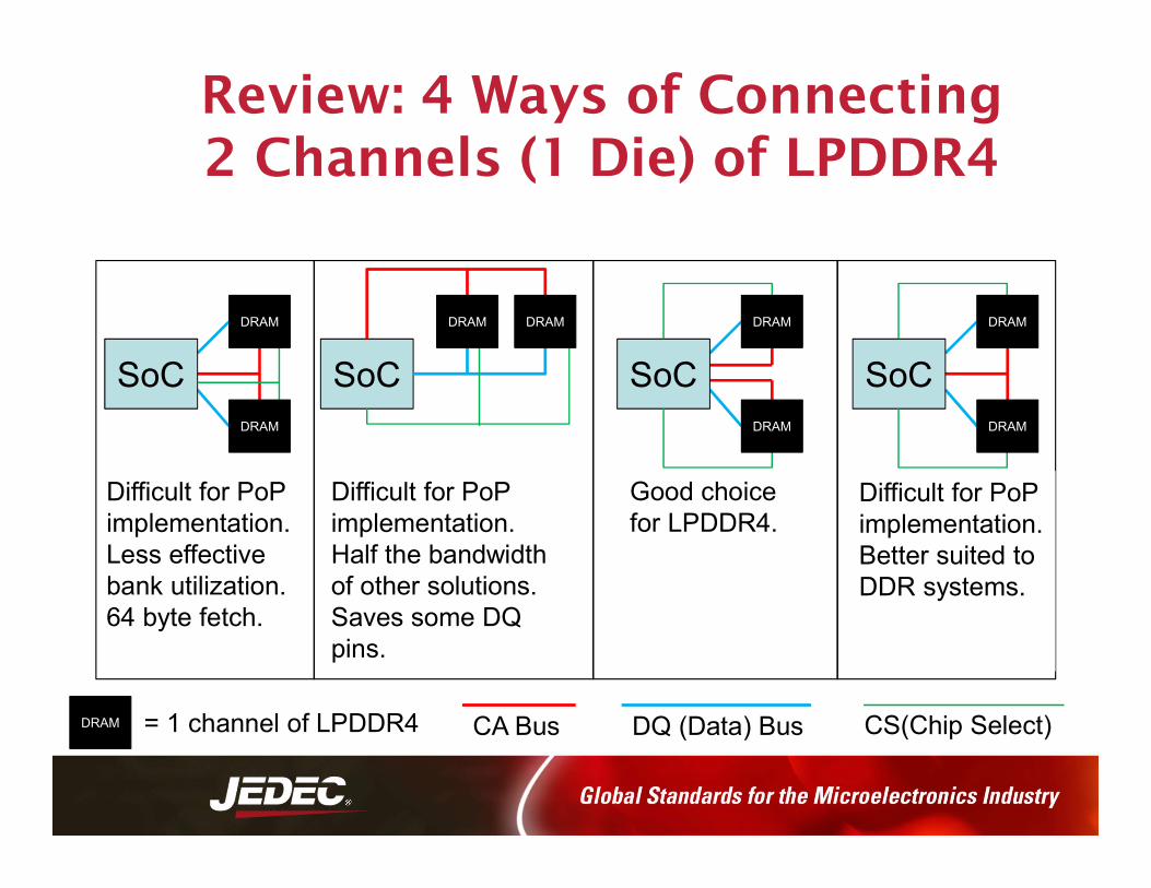
Review: 4 Ways of Connecting 2 Channels (1 Die) of LPDDR4
SoC SoC SoC SoC
ParallelCA pins: 6DQ pins: 32CS pins: 1Banks: 8Fetch: 64
SeriesCA pins: 6DQ pins: 16CS pins: 1Banks: 8Fetch: 32
Multi-channelCA pins: 12DQ pins: 32CS pins: 2Banks: 16Fetch: 32
Shared-CACA pins: 6DQ pins: 32CS pins: 2Banks: 16Fetch: 32/64
DRAM = 1 channel of LPDDR4 CA Bus DQ (Data) Bus CS(Chip Select)
DRAMDRAM
DRAM DRAM
DRAM
DRAM
DRAM DRAM
Review: 4 Ways of Connecting 2 Channels (1 Die) of LPDDR4
SoC SoC SoC SoC
ParallelCA pins: 6DQ pins: 32CS pins: 1Banks: 8Fetch: 64
SeriesCA pins: 6DQ pins: 16CS pins: 1Banks: 8Fetch: 32
Multi-channelCA pins: 12DQ pins: 32CS pins: 2Banks: 16Fetch: 32
Shared-CACA pins: 6DQ pins: 32CS pins: 2Banks: 16Fetch: 32
DRAM = 1 channel of LPDDR4 CA Bus DQ (Data) Bus CS(Chip Select)
Difficult for PoP implementation.Less effective bank utilization.64 byte fetch.
Difficult for PoP implementation.Half the bandwidth of other solutions.Saves some DQ pins.
Good choice for LPDDR4.
Difficult for PoP implementation.Better suited to DDR systems.
DRAM
DRAM
DRAM DRAM
DRAM
DRAM
DRAM
DRAM

Introduction / Agenda
• LPDDR4 is different from earlier JEDEC DRAM• Ways to connect LPDDR4 multiple channels• How to handle 2-die and 4-die packages• Dividing memory traffic across channels• Floorplanning and making connections• Using LPDDR4 low power features• Key features of an LPDDR4 solution

8 Ways of Connecting 4 Channels (2 Dies) of LPDDR4
DRAM = 1 channel of LPDDR4 CA Bus DQ (Data) Bus CS(Chip Select)
SoC
SoC SoCSoC
SoC SoCSoC
SoC

8 Ways of Connecting 4 Channels (2 Dies) of LPDDR4
DRAM = 1 channel of LPDDR4 CA Bus DQ (Data) Bus CS(Chip Select)
SoC
SoC SoCSoC
SoC SoCSoC
SoC
Some are goodSome are not!
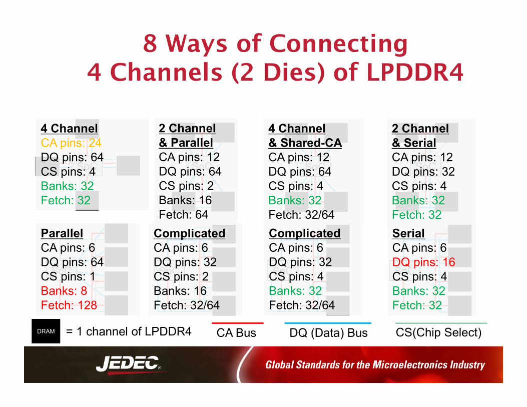
8 Ways of Connecting 4 Channels (2 Dies) of LPDDR4
DRAM = 1 channel of LPDDR4 CA Bus DQ (Data) Bus CS(Chip Select)
SoC
SoC SoCSoC
SoC SoCSoC
SoC
4 ChannelCA pins: 24DQ pins: 64CS pins: 4Banks: 32Fetch: 32
2 Channel& ParallelCA pins: 12DQ pins: 64CS pins: 2Banks: 16Fetch: 64
ParallelCA pins: 6DQ pins: 64CS pins: 1Banks: 8Fetch: 128
4 Channel& Shared-CACA pins: 12DQ pins: 64CS pins: 4Banks: 32Fetch: 32/64
2 Channel& SerialCA pins: 12DQ pins: 32CS pins: 4Banks: 32Fetch: 32SerialCA pins: 6DQ pins: 16CS pins: 4Banks: 32Fetch: 32
ComplicatedCA pins: 6DQ pins: 32CS pins: 4Banks: 32Fetch: 32/64
ComplicatedCA pins: 6DQ pins: 32CS pins: 2Banks: 16Fetch: 32/64

Suggested 2-Die LPDDR4 Implementations
SoC
4 ChannelCA pins: 24DQ pins: 64CS pins: 4Banks: 32Fetch: 32
SoC
2 Channel& ParallelCA pins: 12DQ pins: 64CS pins: 2Banks: 16Fetch: 64
Most familiar implementation especially for LPDDR3 users & LPDDR3/LPDDR4 combination
Most flexible and potentially highest performance
DRAM = 1 channel of LPDDR4 CA Bus DQ (Data) Bus CS(Chip Select)

Expanding to Quad-die
SoC
DRAM = 1 channel of LPDDR4 CA Bus DQ (Data) Bus CS(Chip Select)
SoC
Example 2-die LPDDR4 multichannelimplementation Example 4-die LPDDR4 multichannel
and serial implementation adds DRAM capacity. This solution is compatible with 2-die packages.

Introduction / Agenda
• LPDDR4 is different from earlier JEDEC DRAM• Ways to connect LPDDR4 multiple channels• How to handle 2-die and 4-die packages• Dividing memory traffic across channels• Floorplanning and making connections• Using LPDDR4 low power features• Key features of an LPDDR4 solution

SoC Partitioning for LPDDR4 PoP
Channel A
Channel B
Channel C
Channel D
Channel A
Channel B
Channel C
Channel D
LPDDR4 PackageBallout
SoC MemoryController and
PHY placement sbould be close to
LPDDR4 ballout
LPDDR4 package SoC layout

SoC Partitioning for LPDDR4 PoP
Channel A
Channel B
Channel C
Channel D
Channel A
Channel B
Channel C
Channel D

Real Examples:Five LPDDR4 chip floorplans
4x16bitLPDDR4-onlyApplications Processors
2x32bitLPDDR4-onlyApplications processor
1X64bitDDR4/LPDDR4Special purpose
SoC Chip AreaLPDDR4 area
Sizes/locations are approximate and not to scale. Images derived from commercially purchased chips. Chips shown include Synopsys and non-Synopsys designs.

Dual Channel Block DiagramDDR area on chipschematic view
• Good option for LPDDR4/LPDDR3 combo• 2 channels can share one set of on-chip busses or two sets

© 2015 Synopsys, Inc. 25
Dual Channel Floorplan
• Good option for LPDDR4/LPDDR3 combo• 2 channels can share one set of on-chip busses or two sets
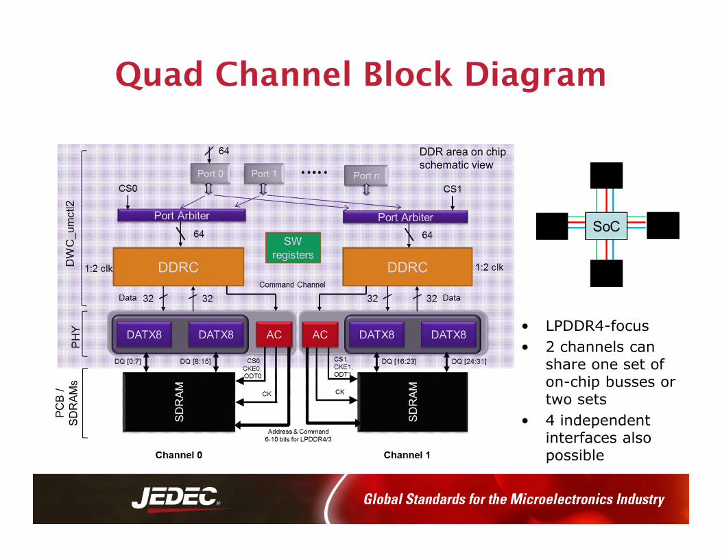
Quad Channel Block DiagramDDR area on chipschematic view
• LPDDR4-focus• 2 channels can share one set of on-chip busses or two sets• 4 independent interfaces also possible

© 2015 Synopsys, Inc. 27
Quad Channel Floorplan
• LPDDR4-focus• 2 channels can share one set of on-chip busses or two sets• 4 independent interfaces also possible

Introduction / Agenda
• LPDDR4 is different from earlier JEDEC DRAM• Ways to connect LPDDR4 multiple channels• How to handle 2-die and 4-die packages• Dividing memory traffic across channels• Floorplanning and making connections• Using LPDDR4 low power features• Key features of an LPDDR4 solution

Three key areas to save power• Use DRAM low-power states
– Powerdown, Self-Refresh– Automatic Entry & Exit by controller
• Different channels in different power states– “Always On Always Connected” data in one channel– Control by logical to physical address map
• Frequency Changing– Change drive & termination with frequency

Logical to Physical Address MapLogical Address
Y MByte
X MByte
0
Operating System and “always on
always connected” functions
Application data, video buffer, etc
Channel A Channel B
Physical locationSeparate Memory MapConsecutive addresses are in one memory channel or the otherThe address ranges do not overlap between channelsGood for power control
Two memory channels are completely different memory spaces

Logical to Physical Address MapLogical Address
Y MByte
X MByte
0 Channel A Channel B
Physical locationInterleaved Memory MapConsecutive addresses are striped across both memory channelsGood for load balancing, not good for power
The whole logical space is interleaved across the whole memory

Logical to Physical Address Map
Operating System and “always on
always connected” functions
Logical Address
Y MByte
X MByte
0
Memory for high-performance and video functions may be interleaved across both memory channels to distribute traffic when both channels are on
Memory for programs that are
associated with high
bandwidth
Channel A Channel B
Physical location
Hybrid Memory MapDifferent regions in each channel are used to provide high bandwidth and controllable power

LPDDR4 Use Model for Mobile Devices
1%LPDDR43200Mbps – 4267MbpsHighest performance9%200-1600Mbps (LPDDR3 range)Phone, browse, photograph, text, read, puzzles, easy gamesBalance performance and power
90%Off or low speed, one channel activeDevice dark and in pocket or at bedsideMaintain cell contact, receive texts, receive and display push notifications, sync mail, show clock, Longest battery life
Drives replacement cycle Performance Focus
Power Focus
Best Performance under low-
speed power limits

Introduction / Agenda
• LPDDR4 is different from earlier JEDEC DRAM• Ways to connect LPDDR4 multiple channels• How to handle 2-die and 4-die packages• Dividing memory traffic across channels• Floorplanning and making connections• Using LPDDR4 low power features• Key features of an LPDDR4 solution

Checklist – Key features of LPDDR4 SoC solution
• Max Operation frequency (32004266MT/s)• Power, Performance, Bandwidth, Latency, Area• Flexible Chip-Level Implementation• Multi-Channel Implementation• Use LPDDR4 power states• Control of logical to physical address map• Use frequency changing• Change drive & termination with frequency• Special Features
– ECC & reliability for Automotive, Temperature monitor & change, refresh flexibility, …

Conclusions• LPDDR4 multichannel architecture provides new opportunities for novel system architectures• LPDDR4 multichannel architecture can improve performance and save power • Consider performance, power, and complexity when considering your LPDDR4 architecture


