High Definition AudioSoundMAX Codec
AD1882A
Rev. 0Information furnished by Analog Devices is believed to be accurate and reliable.However, no responsibility is assumed by Analog Devices for its use, nor for anyinfringements of patents or other rights of third parties that may result from its use.Specifications subject to change without notice. No license is granted by implicationor otherwise under any patent or patent rights of Analog Devices. Trademarks andregistered trademarks are the property of their respective owners.
One Technology Way, P.O.Box 9106, Norwood, MA 02062-9106 U.S.A.Tel: 781.329.4700 www.analog.comFax: 781.461.3113 ©2008 Analog Devices, Inc. All rights reserved.
FEATURESSix 192 kHz, 95 dB DACs
All independent sample rates, 8 kHz through 192 kHz16-, 20-, and 24-bit PCM resolutionSelectable stereo mixer on outputs
Four 192 kHz, 90 dB ADCsSimultaneous record of up to 2 stereo channelsAll independent sample rates, 8 kHz through 192 kHz16-, 20-, and 24-bit resolution
S/PDIF outputSupports all sample rates 44.1 kHz through 192 kHz16-, 20-, and 24-bit data widths; PCM and AC3 formatsDigital PCM gain control
Dedicated auxiliary pinsStereo CD input w/GND senseMono out pin for internal speaker with EAPD supportAnalog PCBeep input pin
Stereo digital microphoneTwo 192 kHz digital microphone channelsSupports 1 or 2 microphones on 1 pinSelectable bit clock rates of 1.5 MHz, 2.0 MHz, and 3.0 MHzAll sample rates, 8 kHz through 192 kHz16-, 20-, and 24-bit resolution
Microsoft Vista Premium® logo for notebook and desktopImpedance and presence detection on all jack pins2 general-purpose digital I/O (GPIO) pinsAdvanced power management modesEAPD control for internal speakers3.3 V analog and digital supply voltage1.5 V and 3.3 V HD Audio link signalingVery low power consumption in D3 state
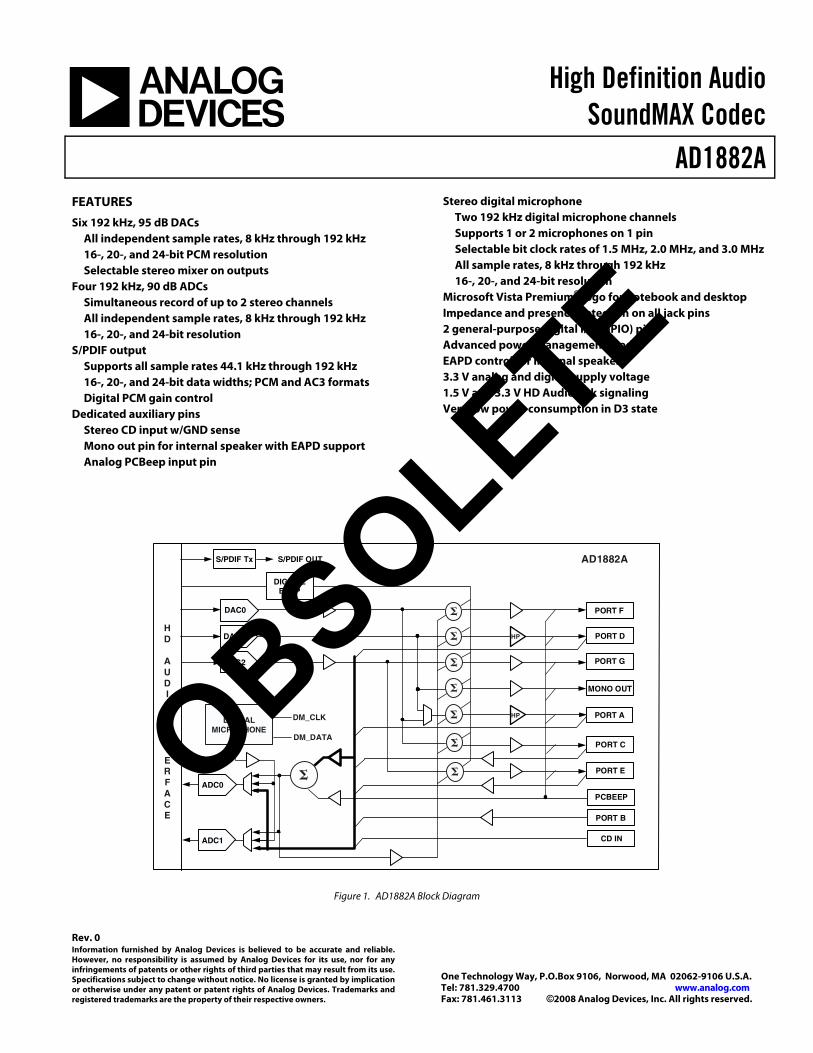
Figure 1. AD1882A Block Diagram
ADC0
ADC1
DAC2
PORT D
PORT F
PORT G
MONO OUT
AD1882A
HD
AUDIO
INTERFACE
PORT A
PORT C
DAC0
HP
HP
�
�
�
�
�
DAC1
PCBEEP
CD IN
�
�
PORT E
PORT B
�
DIGITALMICROPHONE
DM_DATA
DM_CLK
DIGITALBEEP
S/PDIF OUTS/PDIF Tx
OBSOLETE

Rev. 0 | Page 2 of 20 | August 2008
AD1882A
CONTENTSFeatures . . . . . . . . . . . . . . . . . . . . . . . . . . . . . . . . . . . . . . . . . . . . . . . . . . . . . . . . . . . . . . . . . 1Contents . . . . . . . . . . . . . . . . . . . . . . . . . . . . . . . . . . . . . . . . . . . . . . . . . . . . . . . . . . . . . . . . 2Revision History . . . . . . . . . . . . . . . . . . . . . . . . . . . . . . . . . . . . . . . . . . . . . . . . . . . . . . 2General Description . . . . . . . . . . . . . . . . . . . . . . . . . . . . . . . . . . . . . . . . . . . . . . . . . 3
Special Software Features . . . . . . . . . . . . . . . . . . . . . . . . . . . . . . . . . . . . . . . . 3Additional Information . . . . . . . . . . . . . . . . . . . . . . . . . . . . . . . . . . . . . . . . . . 3Jack Configuration . . . . . . . . . . . . . . . . . . . . . . . . . . . . . . . . . . . . . . . . . . . . . . . . 3
Specifications . . . . . . . . . . . . . . . . . . . . . . . . . . . . . . . . . . . . . . . . . . . . . . . . . . . . . . . . . . 4Test Conditions . . . . . . . . . . . . . . . . . . . . . . . . . . . . . . . . . . . . . . . . . . . . . . . . . . . . 4Performance . . . . . . . . . . . . . . . . . . . . . . . . . . . . . . . . . . . . . . . . . . . . . . . . . . . . . . . . 4General Specifications . . . . . . . . . . . . . . . . . . . . . . . . . . . . . . . . . . . . . . . . . . . . 4HD Audio Link Specifications . . . . . . . . . . . . . . . . . . . . . . . . . . . . . . . . . . 6Power-Down States . . . . . . . . . . . . . . . . . . . . . . . . . . . . . . . . . . . . . . . . . . . . . . . 6Absolute Maximum Ratings . . . . . . . . . . . . . . . . . . . . . . . . . . . . . . . . . . . . 7ESD Caution . . . . . . . . . . . . . . . . . . . . . . . . . . . . . . . . . . . . . . . . . . . . . . . . . . . . . . . . 7Environmental Conditions . . . . . . . . . . . . . . . . . . . . . . . . . . . . . . . . . . . . . . 7
Pin Configuration and Function Descriptions . . . . . . . . . . . . . . . . . 8Digital Microphone Interface Timing Specifications . . . . . . . 11HD Audio Parameters . . . . . . . . . . . . . . . . . . . . . . . . . . . . . . . . . . . . . . . . . . . . . 12Widget Parameters . . . . . . . . . . . . . . . . . . . . . . . . . . . . . . . . . . . . . . . . . . . . . . . . . 13HD Audio Widgets . . . . . . . . . . . . . . . . . . . . . . . . . . . . . . . . . . . . . . . . . . . . . . . . 14Connection List . . . . . . . . . . . . . . . . . . . . . . . . . . . . . . . . . . . . . . . . . . . . . . . . . . . . . 15Default Configuration Bytes . . . . . . . . . . . . . . . . . . . . . . . . . . . . . . . . . . . . . 16Outline Dimensions . . . . . . . . . . . . . . . . . . . . . . . . . . . . . . . . . . . . . . . . . . . . . . . 17Ordering Guide . . . . . . . . . . . . . . . . . . . . . . . . . . . . . . . . . . . . . . . . . . . . . . . . . . . . . 17
REVISION HISTORY8/08—Revision 0: Initial Version
OBSOLETE

AD1882A
Rev. 0 | Page 3 of 20 | August 2008
GENERAL DESCRIPTIONThe AD1882A audio codec and SoundMAX® software provides superior HD audio quality that exceeds Vista Premium perfor-mance. The AD1882A has six DACs and four ADCs, two stereo headphone ports, C/LFE swapping, digital and analog PCBeep, and S/PDIF output, making the AD1882A the right choice for desktop and notebook PCs where performance is the primary consideration. The jack retasking feature on this product supports various con-figurations including platforms for 5.1 on 5 or 3 jacks, and front panel jack retasking.The AD1882A is available in a 48-lead Pb-free lead frame chip scale package in both reels and trays. See Ordering Guide on Page 17.
SPECIAL SOFTWARE FEATURESThe AD1882A audio codec also supports the following addi-tional software features:
• BlackHawk® and SoundMAX GUI contain all user audio controls
• Voice input enhancements: Andrea Electronics best-in-class noise reduction, beam forming, and echo cancellation
• Output enhancements: Sensaura/Sonic Focus, spread-ing/downmixing, MP3 refinement, adaptive dynamics, compressor/limiter, speaker/graphic EQ, Voice Clarity/X-MatrixTM, AGC, UI tuning tools
• DTS®, SRS®, EAX for gaming
ADDITIONAL INFORMATIONThis data sheet provides a general overview of the AD1882A SoundMAX codec’s architecture and functionality. Additional information on the AD1882A is available in the AD1882A Pro-grammers Reference Manual. Please contact your local Analog Devices, Inc., sales representative for more information. For information on SoundMAX codecs and software, see Analog Devices website at http://www.analog.com/soundMAX.
JACK CONFIGURATIONThe guidelines shown in Table 1 through Table 4 should be used when selecting ports for particular functions.
Table 1. Typical Desktop Configuration with Discrete Jacks
Port FunctionPort A Front Panel HeadphonePort B Front Panel MicrophonePort C Rear Panel Line-InPort D Rear Panel Line-Out/HeadphonePort E Rear Panel MicrophonePort F Rear Panel SurroundPort G Rear Panel C/LFE
Table 2. Typical Desktop Configuration with 5.1 on 3 Jacks
Port FunctionPort A Front Panel HeadphonePort B Front Panel MicrophonePort C Rear Panel Line-In/SurroundPort D Rear Panel Line-Out/HeadphonePort E Rear Panel Microphone/C/LFE
Table 3. Typical Notebook Configuration
Port FunctionPort A HeadphonePort B MicrophonePort C Internal MicrophonePort D Internal Stereo SpeakersPort E Docking Station Line/Microphone In
Table 4. Typical Notebook Configuration with Digital Microphone
Port FunctionPort A HeadphonePort B MicrophoneDigital Microphone Internal MicrophonePort D Internal Stereo SpeakersPort E Docking Station Line/Microphone InOBSOLETE

Rev. 0 | Page 4 of 20 | August 2008
AD1882A
SPECIFICATIONSTEST CONDITIONS
PERFORMANCE
GENERAL SPECIFICATIONS
Parameter Test ConditionTemperatureDigital Supply Analog SupplyMIC_BIAS_IN (via Low-Pass Filter)Sample Rate fS
Input Signal (Frequency Sine Wave) Amplitude for THD + N Analog Output Pass Band
25°C3.3 V3.3 V5.0 V48 kHz1008 Hz–3.0 dB Full Scale20 Hz to 20 kHz
DAC 10 kΩ Output Load: Line-Out Tests32 Ω Output Load: Headphone Tests
ADC 0 dB Gain
Parameter Min Typ Max UnitLine-Out Drive (10 kΩ Loads—DAC to Pin) Total Harmonic Distortion (THD + N) Dynamic Range (–60 dB in Ref to fS A-Weighted) Signal-to-Noise Ratio
–85 95 95
dBdBdB
Headphone Drive (32 Ω Loads—DAC to Pin) Total Harmonic Distortion (THD + N) Dynamic Range (–60 dB in Ref to fS A-Weighted) Signal-to-Noise Ratio
–83 95 95
dBdBdB
Input Ports (Pin to ADC, Mic Boost = 0 dB) Total Harmonic Distortion (THD + N) Dynamic Range (–60 dB in Ref to fS A-Weighted) Signal-to-Noise Ratio
–81 90 90
dBdBdB
Parameter Min Typ Max UnitDIGITAL DECIMATION AND INTERPOLATION FILTERS—fS = 8 kHz to 96 kHz1
Pass Band 0 0.4 fS HzPass-Band Ripple ±0.005 dBStop Band 0.6 fS HzStop-Band Rejection dBGroup Delay +20 –100 1/fS
Group Delay Variation Over Pass Band 0 μsANALOG-TO-DIGITAL CONVERTERS
Resolution 24 BitsGain Error (Full-Scale Span Relative to Nominal Input Voltage)2 ±10 %Interchannel Gain Mismatch (Difference of Gain Errors) ±0.5 dBADC Offset Error1 ±5 mVADC Crosstalk1
Line Inputs (Input L, Ground R, Read R; Input R, Ground L, Read L) –85 dB Line Inputs to Other –100 –80 dB
OBSOLETE

AD1882A
Rev. 0 | Page 5 of 20 | August 2008
DIGITAL-TO-ANALOG CONVERTERSResolution 24 BitsGain Error (Full-Scale Span Relative to Nominal Input Voltage)1 ±10 %Interchannel Gain Mismatch (Difference of Gain Errors) ±0.5 dBDAC Crosstalk dB (Input L, Zero R, Read R_OUT; Input R, Zero L, Read L_OUT)1 –95 dB
DAC VOLUMESStep Size (DAC0, DAC1, DAC2) 1.5 dBOutput Gain/Attenuation Range –58.5 0 dBMute Attenuation of 0 dB Fundamental1 –80 dB
ADC VOLUMESStep Size (ADCSEL-0, ADCSEL-1) 1.5 dBPGA Gain/Attenuation Range –58.5 +22.5 dBMute Attenuation of 0 dB Fundamental1 –80 dB
ANALOG MIXERSignal-to-Noise Ratio (SNR) Input to Output 95 dBStep Size: All Mixer Inputs 1.5 dBInput Gain/Attenuation Range: All Mixer Inputs –34.5 +12.0 dB
ANALOG LINE LEVEL OUTPUTSFull-Scale Output Voltage 1.0 V rms3
Ports C, E, F, and G Mono Out 2.83 V p-pOutput Impedance1 300 ΩExternal Load Impedance1 10 kΩOutput Capacitance1 15 pFExternal Load Capacitance1 1000 pF
ANALOG HP DRIVE OUTPUTSFull-Scale Output Voltage 1.0 V rms3
Ports A and D 2.83 V p-pOutput Impedance1 0.5 ΩExternal Load Impedance1 32 ΩOutput Capacitance1 15 pFExternal Load Capacitance1 1000 pF
ANALOG INPUTSCD, Port D (When Used as Input) 1
2.83V rms3
V p-pMicrophone Boost Amplifier, Ports B, C, or E (When Used as Inputs)
Boost = 0 dB 12.83
V rms3
V p-pBoost = 10 dB 0.316
0.894V rms3
V p-pBoost = 20 dB 0.1
0.283V rms3
V p-pBoost = 30 dB 0.032
0.089V rms3
V p-pInput Impedance1 20 kΩInput Capacitance1 5 7.5 pF
DIGITAL GPIO PINS: GPIO_0, GPIO_1/EAPDInput Signal High (VIH) DVGPIO × 0.60 DVGPIO VInput Signal Low (VIL) 0 DVGPIO × 0.24 VInput Leakage Current (Signal High), (IIH) 150 nAInput Leakage Current (Signal Low), (IIL) 50 μAOutput Signal High (VOH) IOUT = –500 μA DVGPIO × 0.72 DVGPIO VOutput Signal Low (VOL) IOUT = +1500 μA 0 DVGPIO × 0.10 V
DM_CLKOutput Signal High (VOH) IOUT = –500 μA DVGPIO × 0.72 DVGPIO VOutput Signal Low (VOL) IOUT = +1500 μA 0 DVGPIO × 0.10 V
Parameter Min Typ Max Unit
OBSOLETE

Rev. 0 | Page 6 of 20 | August 2008
AD1882A
HD AUDIO LINK SPECIFICATIONSHD Audio signals comply with the High Definition Audio spec-ifications. Please refer to these specifications at: http://www.intel.com/standards/hdaudio/
POWER-DOWN STATES
DM_DATAInput Signal High (VIH) DVGPIO × 0.60 DVGPIO VInput Signal Low (VIL) 0 DVGPIO × 0.24 VInput Leakage Current (Signal High) (IIH) –150 nAInput Leakage Current (Signal Low) (IIL) –50 nA
S/PDIF_OUTOutput Signal High (VOH) IOUT = –500 μA DVGPIO × 0.72 DVGPIO VOutput Signal Low (VOL) IOUT = +1500 μA 0 DVGPIO × 0.10 V
POWER SUPPLYAnalog (AVDD) 3.3 V ± 5% Power Supply Range Power Dissipation Supply Current
3.13 3.3011635
3.46 VmWmA
Digital (DVDD) 3.3 V ± 10% Power Supply Range Power Dissipation Supply Current
2.97 3.3016249
3.63 VmWmA
Digital I/O (DVIO) 3.3 V ± 10% Power Supply Range Power Dissipation Supply Current
2.97 3.303.961.20
3.63 VmWmA
Digital I/O (DVIO) 1.5 V ± 5.5% Power Supply Range Power Dissipation Supply Current
2.97 3.303.961.20
3.63 VmWmA
Digital GPIO (DVGPIO) 3.3 V ± 10% Power Supply Range Power Dissipation Supply Current
2.97 3.303.631.10
3.63 VmWmA
Power Supply Rejection (100 mV p-p Signal @ 1 kHz)1 80 dB1 Guaranteed but not tested.2 Measurements reflect main ADC.3 RMS values assume sine wave input.
Parameter Min Typ Max Unit
Table 5. Power-Down States
Parameter IDVDD Typ IAVDD Typ UnitFunction Node In D0, All Nodes Active 49 35 mAFunction Node in D3 16 0.7 mACodec in RESET 3 3 mAIndividual Block Power Savings DAC Pair Powered Down Saves (Each) ADC Pair Powered Down Saves (Each) Mixer Power Control (and Associated Amps) Saves MIC_BIAS Powered Down Saves1
1 Powering down the MIC_BIAS powers down all port MIC_BIAS pins. This disables all microphone bias circuits, setting them to the high-Z state.
6500
64.431.0
mAmAmAmA
OBSOLETE

AD1882A
Rev. 0 | Page 7 of 20 | August 2008
ABSOLUTE MAXIMUM RATINGSStresses greater than those listed below may cause permanent damage to the device. This is a stress rating only; functional operation of the device at these or any other conditions above those indicated in the operational section of this specification is not implied. Exposure to absolute maximum rating conditions for extended periods may affect device reliability.
ESD CAUTION
ENVIRONMENTAL CONDITIONSAmbient Temperature Rating:TAMB = TCASE – (PD × θCA)TCASE = case temperature in °CPD = power dissipation in WθCA = thermal resistance (case-to-ambient)θJA = thermal resistance (junction-to-ambient)θJC = thermal resistance (junction-to-case)All measurements per EIA-JESD51 with 2S2P test board per EIA-JESD51-7.
Parameter RatingDigital (DVDD) –0.30 V to +3.65 VDigital I/O (DVIO) –0.30 V to +3.65 VDigital GPIO (DVGPIO) –0.30 V to +3.65 VAnalog (AVDD) –0.30 V to +3.65 VInput Current (Except Supply Pins) ±10.0 mAAnalog Input Voltage (Signal Pins) –0.30 V to AVDD + 0.3 VDigital Input Voltage (Signal Pins) –0.30 V to DVIO + 0.3 VAmbient Temperature (Operating) 0°C to +70°CStorage Temperature –65°C to +150°C
ESD (electrostatic discharge) sensitive device.Charged devices and circuit boards can discharge without detection. Although this product features patented or proprietary protection circuitry, damage may occur on devices subjected to high energy ESD. Therefore, proper ESD precautions should be taken to avoid performance degradation or loss of functionality.
Package θJA θJC θCA UnitLFCSP_VQ 47 15 32 °C/W
OBSOLETE

Rev. 0 | Page 8 of 20 | August 2008
AD1882A
PIN CONFIGURATION AND FUNCTION DESCRIPTIONS
Figure 2. AD1882A 48-Lead Package and Pinout
1
2
3
4
5
6
7
8
9
10
11
12
242313 14 15 16 17 18 19 20 21 22
34
33
36
35
25
26
27
28
29
30
31
32
44 434748 4546 373839404142
AD1882AJCPZ
TOP VIEW
(NotTo Scale)
DVCORE
GPIO_0
DVGPIO
DVIO
SDATA_OUT
BIT_CLK
DVSS
SDATA_IN
DVDD
SYNC
RESET
PCBEEP
PORT-D_R
PORT-D_L
PO
RT
-C_R
PO
RT
-C_L
PO
RT
-B_R
PO
RT
-E_L
PO
RT
-F_R
PO
RT
-F_L
PO
RT
-B_L
PO
RT
-E_R
CD
_L
CD
_R
CD
_GN
D
SE
NS
E_A
/SR
C_B
SENSE_B/SRC_A
PO
RT
-A_L
MO
NO
_OU
T
GP
IO_1
/EA
PD
PO
RT
-G_R
AV
DD
PO
RT
-G_L
PO
RT
-A_R
AV
SS
S/P
DIF
_OU
T
MIC_BIAS_IN
MIC_BIAS-B
MIC_BIAS-C
MIC_BIAS-E
AVDD
AVSS
VREF_FLT
RESERVED (NC)
RESERVED (NC)
DM
_CL
K
DM
_DA
TA
RE
SE
RV
ED
(NC
)
OBSOLETE

AD1882A
Rev. 0 | Page 9 of 20 | August 2008
Table 6. AD1882A Pin Descriptions
Mnemonic Pin No. Function DescriptionDIGITAL INTERFACE SDATA_OUT
BIT_CLK SDATA_IN SYNC RESET
5
6 8 10 11
I
I I/OII
Link Serial Data Output. AD1882A input stream. Clocked on both edges of the BIT_CLK.Link Bit Clock. 24.000 MHz serial data clock. Link Serial Data Input. AD1882A output stream clocked only on one edge of BIT_CLK.Link Frame Sync.Link Reset. AD1882A master hardware reset
DIGITAL I/O GPIO_0 GPIO_1/EAPD
S/PDIF_OUT DM_DATA DM_CLK
2 47
48 4546
I/OI/O
OIO
General-Purpose Input/Output. Supports S/PDIF output as primary function.General-Purpose Input/Output Pin/EAPD Pin. Digital signal used to control external circuitry. By default pin is in a high-Z state. When used as EAPD: high-Z = amp-on, DVSS = amp off.S/PDIF output.Digital Microphone Data Input. Support for 2 digital microphonesDigital Microphone Clock Output.
JACK SENSE AND EAPD SENSE_A/SRC_B SENSE_B/SRC_A
13 34
I/OI/O
JACK SENSE A-D Input/Sense B Drive.JACK SENSE E-H Input/Sense A Drive.
ANALOG I/O PCBEEP PORT-E_L PORT-E_R PORT-F_L PORT-F_R CD_L CD_GND
CD_R PORT-B_L PORT-B_R PORT-C_L PORT-C_R PORT-D_L PORT-D_R PORT-A_L MONO_OUT PORT-A_R PORT-G_L PORT-G_R
12 14 15 16 17 1819 2021 22 23 24 35 36 39 40414344
LI LI, MIC, LO, SWAP LI, MIC, LO, SWAPI/OI/O LI LI
LILI, MIC, HP, LOLI, MIC, HP, LOLI, MIC, LOLI, MIC, LOLI, HP, LO LI, HP, LOLI, MIC, HP, LO LOLI, MIC, HP, LOLO, SWAPLO, SWAP
Monaural Input from System for Analog PCBeep.Auxiliary Input/Output Left Channel. Auxiliary Input/Output Right Channel.Auxiliary Input/Output Left Channel.Auxiliary Input/Output Right Channel. CD Audio Left Channel.CD Audio Analog Ground Reference (for Differential CD Input). Must be connected to AGND via 0.1 μF capacitor if not in use as CD_GND.CD Audio Right Channel.Front Panel Stereo MIC/Line-In. Front Panel Stereo MIC/Line-In.Rear Panel Stereo MIC/Line-In. Rear Panel Stereo MIC/Line-In. Rear Panel Headphone/Line-Out. Rear Panel Headphone/Line-Out. Front Panel Headphone/Line-Out. Monaural Output to Internal Speaker or Telephony Subsystem Speakerphone. Front Panel Headphone/Line-Out.Rear Panel C/LFE Output. Rear Panel C/LFE Output.
FILTER/REFERENCE MIC_BIAS-B MIC_BIAS-C MIC_BIAS-E
28 2931
O O O
Switchable Microphone Bias. For use with Port B (Pins 21, 22).Switchable Microphone Bias. For use with Port C (Pins 23, 24).Switchable Microphone Bias. For use with Port E (Pins 14, 15).
DVCORE 1 O CAUTION: DO NOT APPLY 3.3 V TO THIS PIN!Filter connection for internal core voltage regulator.This pin must be connected to filter caps: 10 μF, 1.0 μF, and 0.1 μF connected in parallel between Pin 1 and DVSS (Pin 4).
VREF_FLT 27 O Voltage Reference Filter. This pin must be connected to filter caps: 1.0 μF and 0.1μF connected in parallel between Pin 27 and AVSS (Pins 26, 42).
The symbols used in this table are defined as: I = input, O = output, LI = line level input, LO = line level output, HP = output capable of driving headphone load, MIC = input supports microphones with MIC bias and boost amplifier, SWAP = outputs can swap L/R channels (typically used to support C/LFE or shared C/LFE function).
OBSOLETE

Rev. 0 | Page 10 of 20 | August 2008
AD1882A
POWER AND GROUND DVIO 3.3 V ± 10% or DVIO 1.5 V ± 5.5%
4 I Connect to the I/O Voltage Used for the HD Audio Controller Signals.
DVGPIO 3 I Connect to 3.3 V digital supply to power the GPIO and S/PDIF pins. DVSS 7 I Digital Supply Return (Ground). DVDD (3.3 V) 9 I Digital Supply Voltage 3.3 V. This is regulated down to DVCORE on Pin 1 to supply the
internal digital core internal to the AD1882A. AVDD (3.3 V) 25, 38 I CAUTION: DO NOT APPLY 5.0 V TO THESE PINS!
Analog Supply Voltage 3.3 V ONLY.Note: AVDD supplies should be well regulated and filtered as supply noise degrades audio performance.
MIC_BIAS_IN 33 I Source Power for Microphone Bias Circuitry. Connect this pin to 5.0 V via a low-pass filter. When connected this way, the AD1882A is capable of providing 3.9 V as a mic bias to all of the MIC_BIAS pins. If 5 V is not available, connect this pin to 3.3 V (AVDD) via a low-pass filter.
AVSS 26, 42 I Analog Supply Return (Ground). AVSS should be connected to DVSS using a conductive trace under, or close to, the AD1882A.
Table 6. AD1882A Pin Descriptions (Continued)
Mnemonic Pin No. Function Description
The symbols used in this table are defined as: I = input, O = output, LI = line level input, LO = line level output, HP = output capable of driving headphone load, MIC = input supports microphones with MIC bias and boost amplifier, SWAP = outputs can swap L/R channels (typically used to support C/LFE or shared C/LFE function).
OBSOLETE

AD1882A
Rev. 0 | Page 11 of 20 | August 2008
DIGITAL MICROPHONE INTERFACE TIMING SPECIFICATIONSThe digital microphone interface can support one or two digital microphones using two or three codec pins. Both uniplex (one microphone per data pin) and multiplex (two microphones sharing the same data pin) are supported. The timing for these
configurations are shown in Figure 3 and Figure 4. The interface can generate a microphone clock at 1.5 MHz, 2.0 MHz, or 3.0 MHz to suit quality and power requirements.
Table 7. Microphone Timing Parameters
Parameter Min Typ Max UnitTiming Requirementst0 DM_CLK (1.5 MHz) Period
Duty Cycle66750/50
ns%
t0 DM_CLK (2.0 MHz) Period Duty Cycle
50050/50
ns%
t0 DM_CLK (3.0 MHz) Period Duty Cycle
33350/50
ns%
t1 DM_CLK Rise Time 5 nst2 DM_CLK Fall Time 5 nst3 Data Setup to DM_CLK Edge 100 nst4 Data Hold from DM_CLK Edge 5 ns
Figure 3. Uniplex Microphone Timing
Figure 4. Multiplex Microphone Timing
DM_CLK
t1
t2
t3
DM_DATA
t0
t4
DM_CLK
t1 t2
t3
DM_DATA
t0
LEFT DATA VALID RIGHT DATA VALID LEFT DATA VALID
t4 t3 t4OBSOLETE
Rev. 0 | Page 12 of 20 | August 2008
AD1882A
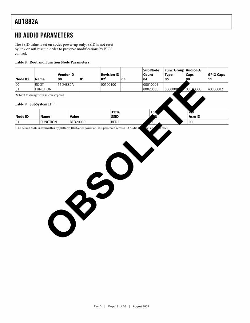
HD AUDIO PARAMETERSThe SSID value is set on codec power-up only. SSID is not reset by link or soft reset in order to preserve modifications by BIOS control.
Table 8. Root and Function Node Parameters
Node ID NameVendor ID00 01
Revision ID021 03
Sub Node Count04
Func. Group Type05
Audio F.G. Caps08
GPIO Caps11
00 ROOT 11D4882A 00100100 0001000101 FUNCTION 0002003B 00000001 00010C0C 40000002
1 Subject to change with silicon stepping.
Table 9. SubSystem ID 1
Node ID Name Value31:16SSID
15:8 SKU
7:0Asm ID
01 FUNCTION BFD20000 BFD2 00 001 The default SSID is overwritten by platform BIOS after power on. It is preserved across HD Audio link reset and verb reset.
OBSOLETE

AD1882A
Rev. 0 | Page 13 of 20 | August 2008
WIDGET PARAMETERSTable 10. Widget Parameters
Node ID
Widget Capabilities 09
PCM Size, Rate0A
Stream Formats 0B
Pin Capabilities 0C
Input Amp Capabilities 0D
ConnList Length 0E
Power States 0F
Output Amp Capabilities 12
01 0x0000 0480 0x000E 07FF 0x0000 0001 0x80000000 0x0000 0009 0x0005 272702 0x0003 031D 0x000E 07E0 0x0000 0005 0x0000 0001 0x8005 272703 0x0000 0405 0x000E 07FF 0x0000 0001 0x0000 0000 0x0000 0009 0x0005 272704 0x0000 0405 0x000E 07FF 0x0000 0001 0x0000 0000 0x0000 0009 0x0005 272705 0x0000 0405 0x000E 07FF 0x0000 0001 0x0000 0000 0x0000 0009 0x0005 272708 0x0010 0501 0x000E 07FF 0x0000 0001 0x0000 0001 0x0000 000909 0x0010 0501 0x000E 07FF 0x0000 0001 0x0000 0001 0x0000 00090C 0x0030 010D 0x0000 0008 0x8005 36270D 0x0030 010D 0x0000 0008 0x8005 362710 0x0070 000C 0x0000 0000 0x800B 0F0F11 0x0040 058D 0x0000 373F 0x0000 0001 0x8000 000012 0x0040 058D 0x0001 003F 0x0000 0001 0x0000 0009 0x8000 000013 0x0040 050C 0x0001 0010 0x0000 0001 0x0000 0009 0x8005 1F1F14 0x0040 0081 0x0000 3727 0x0000 000015 0x0040 018D 0x0000 3737 0x0000 0001 0x8000 000016 0x0040 058D 0x0001 0017 0x0000 0001 0x0000 0009 0x8000 000017 0x0040 098D 0x0000 3737 0x0000 0001 0x8000 000018 0x0040 0081 0x0000 0024 0x0000 000019 0x0050 0500 0x0000 0002 0x0000 00091A 0x0040 0000 0x0000 0020 0x0000 00001B 0x0040 0301 0x0000 0010 0x0000 00011E 0x0020 0103 0x8000 0000 0x0000 00021F 0x0040 000B 0x0000 0020 0x0017 0300 0x0000 000020 0x0020 010B 0x8005 1F17 0x0000 000821 0x0030 010D 0x0000 0001 0x8005 1F1F22 0x0020 0103 0x8000 0000 0x0000 000223 0x00F0 0100 0x0000 000824 0x0040 098D 0x0000 0017 0x0000 0001 0x8000 000026 0x0020 0103 0x8000 0000 0x0000 000227 0x0020 0103 0x8000 0000 0x0000 000229 0x0020 0103 0x8000 0000 0x0000 00022A 0x0020 0103 0x8000 0000 0x0000 00022C 0x0020 0103 0x8000 0000 0x0000 00022D 0x0020 0100 0x0000 00012F 0x00F0 0100 0x0000 000337 0x0030 0101 0x0000 000239 0x0030 010D 0x0000 0001 0x0027 03003A 0x0030 010D 0x0000 0001 0x0027 03003C 0x0030 010D 0x0000 0001 0x0027 0300OBSOLETE

Rev. 0 | Page 14 of 20 | August 2008
AD1882A
HD AUDIO WIDGETSIn the following table, node IDs that are not shown are reserved for future use.
Table 11. HD Audio Widgets
Node ID Name Type ID Type Description00 ROOT x Root Device Identification01 FUNCTION x Function Designates this Device as an Audio Codec02 S/PDIF DAC 0 Audio Output S/PDIF Digital Stream Output Interface03 DAC_0 0 Audio Output Headphone/Surround Side (7.1) Channel Digital/Audio Converters04 DAC_1 0 Audio Output Stereo Front Channel Digital/Audio Converters05 DAC_2 0 Audio Output Stereo C/LFE Channel Digital/Audio Converters08 ADC_0 1 Audio Input Stereo Record Channel 1 Audio/Digital Converters09 ADC_1 1 Audio Input Stereo Record Channel 2 Audio/Digital Converters0C ADC Selector 0 3 Audio Selector Selects and Amplifies/Attenuates the Input to ADC00D ADC Selector 1 3 Audio Selector Selects and Amplifies/Attenuates the Input to ADC110 Digital Beep 7 Beep Generator Internal Digital PCBeep Signal11 Port A (Headphone) 4 Pin Complex Front Panel Headphone/Microphone Jack12 Port D (Front L/R) 4 Pin Complex Rear Panel Front/Headphone Jack13 Mono Out 4 Pin Complex Monorail Output Pin (Internal Speakers or Telephony System)14 Port B (Front Mic) 4 Pin Complex Front Panel Microphone/Headphone Jack15 Port C (Line In) 4 Pin Complex Rear Panel Line-In Jack16 Port F (Surr Back) 4 Pin Complex Rear Panel Surround-Rear (5.1) Jack17 Port E (Rear Mic) 4 Pin Complex Rear Panel Mic Jack18 CD In 4 Pin Complex Analog CD Input19 Mixer Power Down 5 Power Widget Powers Down the Analog Mixer and Associated Amps1A Analog PCBeep 4 Pin Complex External Analog PCBeep Signal Input1B S/PDIF Out 4 Pin Complex S/PDIF Output Pin1E Mono Out Mixer 2 Audio Mixer Selects Which Source Drives the Mono Out Signal1F Digital Microphone 4 Pin Complex Digital Microphone Interface20 Analog Mixer 2 Audio Mixer Mixes Individually Gainable Analog Inputs21 Mixer Output Atten 3 Audio Selector Attenuates the Mixer Output to Drive the Port Mixers22 Port A Mixer 2 Audio Mixer Mixes the Port A Selected DAC and Mixer Output Amps to Drive Port A23 VREF Power Down F Vendor Defined Powers Down the Internal and External VREF Circuitry24 Port G (C/LFE) 4 Pin Complex Rear Panel C/LFE Jack26 Port E Mixer 2 Audio Mixer Mixes DAC1 and Mixer Output Amps to Drive Port E27 Port G Mixer 2 Audio Mixer Mixes DAC1 and Mixer Output Amps to Drive Port G29 Port D Mixer 2 Audio Mixer Mixes DAC0 and Mixer Output Amps to Drive Port D2A Port F Mixer 2 Audio Mixer Mixes DAC2 and Mixer Output Amps to Drive Port F2C Port C Mixer 2 Audio Mixer Mixes the Port C Selected DAC and Mixer Output Amps to Drive Port C2D Stereo Mix Down 2 Audio Mixer Mixes the Stereo L/R Channels to Drive Mono Output2F BIAS Power Down F Vendor Defined Powers Down the Internal MIC_BIAS_IN and all MIC_BIAS Pins37 Port A Out Selector 3 Audio Selector Selects the Port A DAC (0, 1)39 Port B Boost 3 Audio Selector Microphone Boost Amp for Port B3A Port C Boost 3 Audio Selector Microphone Boost Amp for Port C3C Port E Boost 3 Audio Selector Microphone Boost Amp for Port E
OBSOLETE
AD1882A
Rev. 0 | Page 15 of 20 | August 2008
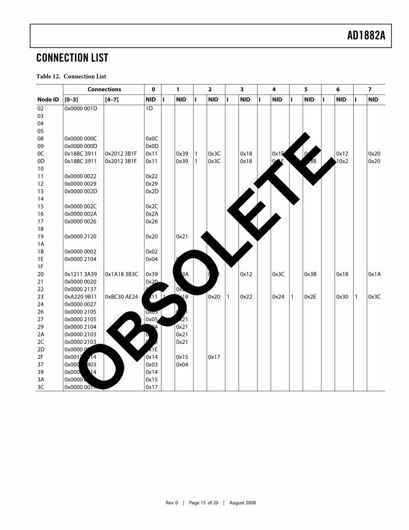
CONNECTION LISTTable 12. Connection List
Connections 0 1 2 3 4 5 6 7
Node ID [0–3] [4–7] NID I NID I NID I NID I NID I NID I NID I NID02 0x0000 001D 1D03040508 0x0000 000C 0x0C09 0x0000 000D 0x0D0C 0x18BC 3911 0x2012 3B1F 0x11 0x39 1 0x3C 0x18 0x1F 0x3B 0x12 0x200D 0x18BC 3911 0x2012 3B1F 0x11 0x39 1 0x3C 0x18 0x1F 0x3B 10x2 0x201011 0x0000 0022 0x2212 0x0000 0029 0x2913 0x0000 002D 0x2D1415 0x0000 002C 0x2C16 0x0000 002A 0x2A17 0x0000 0026 0x261819 0x0000 2120 0x20 0x211A1B 0x0000 0002 0x021E 0x0000 2104 0x04 0x211F20 0x1211 3A39 0x1A18 3B3C 0x39 0x3A 0x11 0x12 0x3C 0x3B 0x18 0x1A21 0x0000 0020 0x2022 0x0000 2137 0x37 0x2123 0xA220 9811 0xBC30 AE24 0x11 1 0x18 0x20 1 0x22 0x24 1 0x2E 0x30 1 0x3C24 0x0000 0027 0x2726 0x0000 2105 0x05 0x2127 0x0000 2105 0x05 0x2129 0x0000 2104 0x04 0x212A 0x0000 2103 0x03 0x212C 0x0000 2103 0x03 0x212D 0x0000 001E 0x1E2F 0x0017 1514 0x14 0x15 0x1737 0x0000 0403 0x03 0x0439 0x0000 0014 0x143A 0x0000 0015 0x153C 0x0000 0017 0x17OBSOLETE

Rev. 0 | Page 16 of 20 | August 2008
AD1882A
DEFAULT CONFIGURATION BYTESIn Table 13, default configuration values are set on codec power-up only. Default configuration values are not reset by link or soft reset to preserve modifications by BIOS control.
Table 13. Default Configuration Bytes
31:30 29:28 27:24 23:20 19:16 15:12 8 7:4 3:0
Connectivity
Location
Def. Device Conn Type Color
Misc.
Def Assn SequenceName Value Chassis Position JDPort A (Headphone) 0x0221 401F Jack External Front HP Out 1/8” Jack Green 0 1 FPort D (Front L/R) 0x0101 4010 Jack External Rear Line Out 1/8” Jack Green 0 1 0Mono Out 0x9017 01F0 Fixed Internal N/A Speaker Other Analog Unknown 1 F 0Port B (Front Mic) 0x02A1 90F0 Jack External Front Mic In 1/8” Jack Pink 0 F 0Port C (Line In) 0x0181 3021 Jack External Rear Line In 1/8” Jack Blue 0 2 1Port F (Surr Back) 0x0101 1012 Jack External Rear Line Out 1/8” Jack Black 0 1 2Port E (Rear Mic) 0x01A1 9020 Jack External Rear Mic In 1/8” Jack Pink 0 2 0CD IN 0x9933 012E Fixed Internal Special 3 CD ATAPI Unknown 1 2 EAnalog PCBeep 0x90F7 01F0 Fixed Internal N/A Other Other Analog Unknown 1 F 0S/PDIF Out 0x0145 11F0 Jack External Rear SPDIF Out Optical Black 1 F 0Digital Microphone 0x97A6 09F0 Fixed Internal Special 1 Mic In Other Digital Unknown 1 F 0Port G (C/LFE) 0x0101 6011 Jack External Rear Line Out 1/8” Jack Orange 0 1 1
OBSOLETE

AD1882A
Rev. 0 | Page 17 of 20 | August 2008
OUTLINE DIMENSIONSDimensions are shown in millimeters.
ORDERING GUIDE
Figure 5. 48-Lead, Lead Frame Chip Scale Package [LFCSP_VQ]7 mm x 7 mm Body, Very Thin Quad
(CP-48-1)Dimensions shown in millimeters
Model Temperature Range Package Description Package OptionAD1882AJCPZ1
1 Z = RoHS Compliant Part.
0°C to 70°C 48-Lead LFCSP_VQ CP-48-1AD1882AJCPZ-RL1 0°C to 70°C 48-Lead LFCSP_VQ, 13” Tape and Reel CP-48-1
COMPLIANT TO JEDEC STANDARDS MO-220-VKKD-2
PIN 1INDICATOR
TOPVIEW
6.75BSC SQ
7.00BSC SQ
148
1213
3736
2425
5.255.10 SQ4.95
0.500.400.30
0.300.230.18
0.50 BSC
12° MAX
0.20 REF
0.80 MAX0.65 TYP
1.000.850.80
5.50REF
0.05 MAX0.02 NOM
0.60 MAX0.60 MAX PIN 1
INDICATOR
COPLANARITY0.08
SEATINGPLANE
0.25 MIN
*EXPOSEDPAD
(BOTTOM VIEW)
*NOTE:THE EXPOSED PAD IS REQUIRED TO BE ELECTRICALLY AND THERMALLY CONNECTED TO VSS. THIS SHOULD BE IMPLEMENTED BY SOLDERING THE EXPOSED PAD TO A VSS PCB LAND THAT IS THE SAME SIZE AS THE EXPOSED PAD. THE VSS PCB LAND SHOULD BE ROBUSTLY CONNECTED TO THE VSS PLANE IN THE PCB WITH AN ARRAY OF THERMAL VIAS FOR BEST PERFORMANCE.
OBSOLETE

Rev. 0 | Page 18 of 20 | August 2008
AD1882A
OBSOLETE

AD1882A
Rev. 0 | Page 19 of 20 | August 2008
OBSOLETE
Rev. 0 | Page 20 of 20 | August 2008
AD1882A
©2008 Analog Devices, Inc. All rights reserved. Trademarks andregistered trademarks are the property of their respective owners.
D07549-0-8/08(0)
OBSOLETE


