© 2010 Eric Pop, UIUC ECE 598EP: Hot Chips 1
Hot Chips: Atoms to Heat SinksECE 598EP
Prof. Eric PopDept. of Electrical and Computer EngineeringUniv. Illinois Urbana-Champaign
http://poplab.ece.illinois.edu

© 2010 Eric Pop, UIUC ECE 598EP: Hot Chips 2
The Big Picture
http://phys.ncku.edu.tw/~htsu/humor/fry_egg.html
XP1500+ CPU

© 2010 Eric Pop, UIUC ECE 598EP: Hot Chips 3
Another CPU without a Heat Sink
Source: Tom’s Hardware Guidehttp://www6.tomshardware.com/cpu/01q3/010917/heatvideo-01.html

© 2010 Eric Pop, UIUC ECE 598EP: Hot Chips 4
Thermal Management Methods
ASUSTeK cooling solution (!)
© 2010 Eric Pop, UIUC ECE 598EP: Hot Chips 5
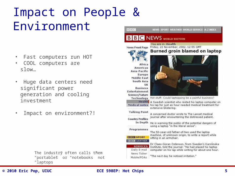
Impact on People & Environment
The industry often calls them“portables” or “notebooks” not “laptops”
• Fast computers run HOT• COOL computers are slow…
• Huge data centers need significant power generation and cooling investment
• Impact on environment?!

© 2010 Eric Pop, UIUC ECE 598EP: Hot Chips
Packaging cost
From Cray (local power generator and refrigeration)…
http://www.research.microsoft.com/users/gbell/craytalk/
6
© 2010 Eric Pop, UIUC ECE 598EP: Hot Chips
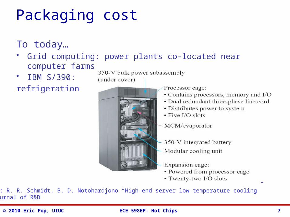
Packaging cost
To today…• Grid computing: power plants co-located near computer farms• IBM S/390:
refrigeration
Source: R. R. Schmidt, B. D. Notohardjono “High-end server low temperature cooling”IBM Journal of R&D
7

© 2010 Eric Pop, UIUC ECE 598EP: Hot Chips
IBM S/390 refrigeration
• Complex and expensive
Source: R. R. Schmidt, B. D. Notohardjono “High-end server low temperature cooling” IBM Journal of R&D
8

© 2010 Eric Pop, UIUC ECE 598EP: Hot Chips
IBM S/390 processor packaging
Processor sub-assembly: complex!
C4: Controlled Collapse Chip Connection (flip-chip)
Source: R. R. Schmidt, B. D. Notohardjono “High-end server low temperature cooling”IBM Journal of R&D
9

© 2010 Eric Pop, UIUC ECE 598EP: Hot Chips
Intel Itanium packaging
Complex and expensive (note heatpipe)
Source: H. Xie et al. “Packaging the Itanium Microprocessor”Electronic Components and Technology Conference 2002
10

© 2010 Eric Pop, UIUC ECE 598EP: Hot Chips
Intel Pentium 4 packaging
• Simpler, but still…
Source: Intel web site
11

© 2010 Eric Pop, UIUC ECE 598EP: Hot Chips
Graphics Cards
• Nvidia GeForce 5900 card
Source: Tech-Report.com
12
© 2010 Eric Pop, UIUC ECE 598EP: Hot Chips
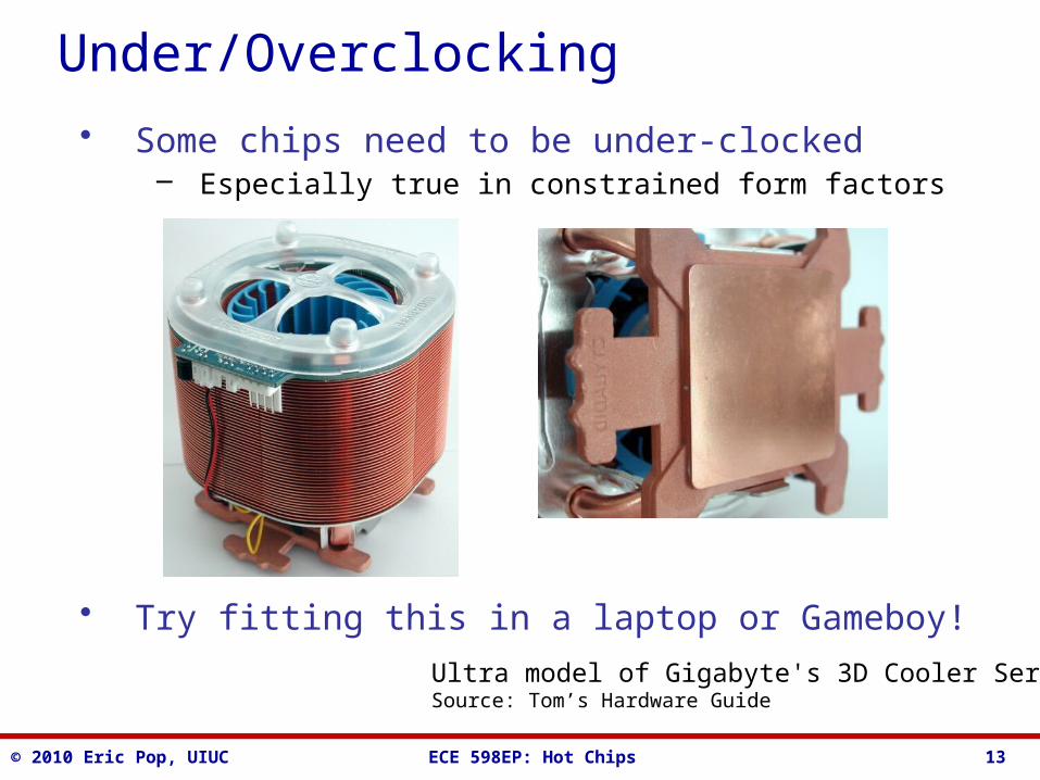
Under/Overclocking
• Some chips need to be under-clocked– Especially true in constrained form factors
• Try fitting this in a laptop or Gameboy!
Ultra model of Gigabyte's 3D Cooler Series Source: Tom’s Hardware Guide
13
© 2010 Eric Pop, UIUC ECE 598EP: Hot Chips
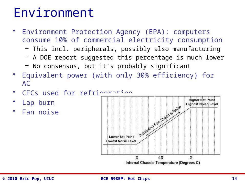
Environment• Environment Protection Agency (EPA): computers consume 10%
of commercial electricity consumption– This incl. peripherals, possibly also manufacturing– A DOE report suggested this percentage is much lower– No consensus, but it’s probably significant
• Equivalent power (with only 30% efficiency) for AC• CFCs used for refrigeration• Lap burn• Fan noise
14

© 2010 Eric Pop, UIUC ECE 598EP: Hot Chips 15
A More Detailed Look
• Data centers + 100 million PCs + displays + cooling = 5 % of nation-wide power budget in 2007
• PCs alone generate pollution equivalent to 5 million cars (state of Maryland!), which would require nearly 2 billion trees to offset
• If current trends continue, computer-related energy use could be 1/3 of US power by 2025
http://www.climatesaverscomputing.orghttp://www.energystar.gov/index.cfm?c=prod_development.server_efficiency_study
0
2
4
6
2000 2006
Data centers(7 GW)
Home PCs(2.6 GW)
Home displays (1.3 GW)
Work displays(3.2 GW)
Work PCs(6.5 GW)
Cooling
Network
Storage
Servers
Total poweruse (2007)
Data centerpower use(GWatts)
© 2010 Eric Pop, UIUC ECE 598EP: Hot Chips
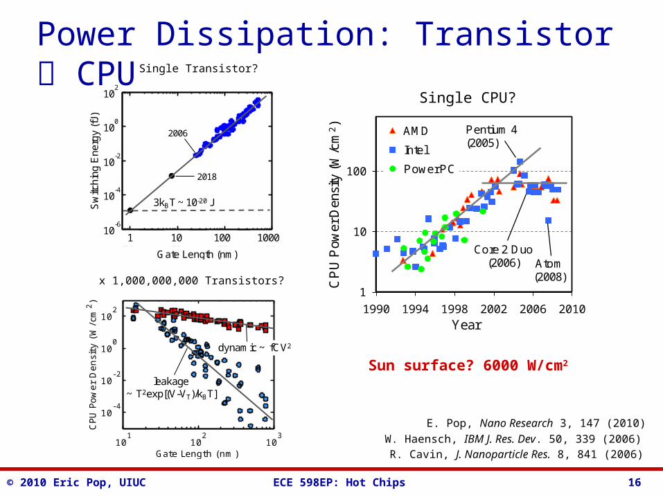
Power Dissipation: Transistor CPU
16
W. Haensch, IBM J. Res. Dev. 50, 339 (2006)R. Cavin, J. Nanoparticle Res. 8, 841 (2006)
Single Transistor?
x 1,000,000,000 Transistors?1
10
100
1990 1994 1998 2002 2006 2010
AMD
Intel
Power PC
CP
U P
ower
Den
sity
(W
/cm
2)
Year
Pentium 4(2005)
Core 2 Duo(2006) Atom
(2008)
Sun surface? 6000 W/cm2
Single CPU?
101
102
103
10-4
10-2
100
102
Gate Length (nm)
CPU
Pow
er
Den
sity
(W
/cm
2)
leakage~T2exp[(V-VT)/kBT]
dynamic ~ fCV2
100
101
102
103
10-6
10-4
10-2
100
102
Gate Length (nm)
Sw
itchi
ng E
nerg
y (f
J)
1 10 100 1000
2006
2018
3kBT ~ 10-20 J
E. Pop, Nano Research 3, 147 (2010)
© 2010 Eric Pop, UIUC ECE 598EP: Hot Chips 17
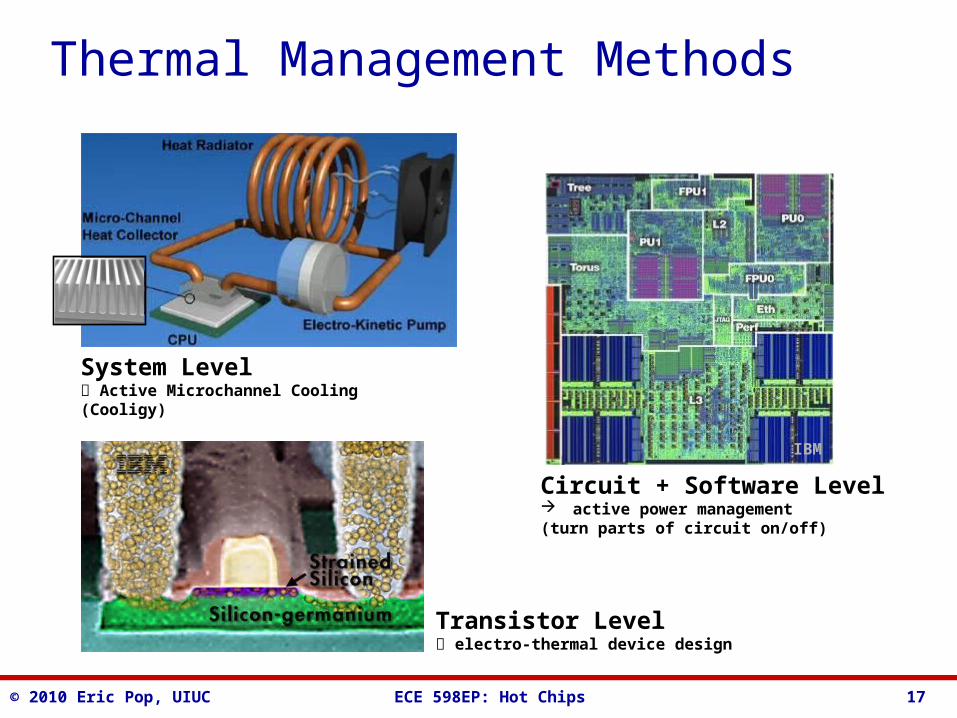
Thermal Management Methods
System Level Active Microchannel Cooling (Cooligy)
Transistor Level electro-thermal device design
Circuit + Software Level active power management(turn parts of circuit on/off)
IBM

© 2010 Eric Pop, UIUC ECE 598EP: Hot Chips 18
Where Does the Heat Come From?
Intel 65 nm
Ttransistors
Rconvection
Ctransistor
Cchip
Cheat sink
Tchip
Rchip
Theat sink
Cinterconnect
Tinterconnect
Tcoolant
heat spreaderSi chip
chip carrier
fan
fin array heat sink
heat spreaderSi chip
chip carrier
fan
fin array heat sink
Rdielectric
Rspreading
Top viewHottest spots > 300 W/cm2
Intel Itanium
Cross-section8 metal levels + ILD
Transistor < 100 nm

© 2010 Eric Pop, UIUC ECE 598EP: Hot Chips 19
More on Chip-Level Complexity
Power dissipationin interconnects
Power dissipationin transistors
Thermal conductivityof substrate, heat sink
Logic Logic
Distributed MemoryDistributed Memory
DRAMDRAM
Analog / RFAnalog / RF
Optical I/OOptical I/O
Logic Logic
Distributed MemoryDistributed Memory
DRAMDRAM
Analog / RFAnalog / RF
Optical I/OOptical I/O
3-D integrated circuits = the ultimate density limit
How do we get the power in?How do we take the heat out?
© 2010 Eric Pop, UIUC ECE 598EP: Hot Chips
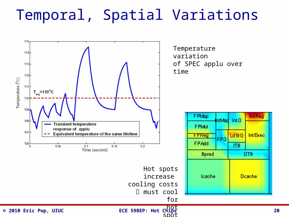
Temporal, Spatial Variations
Temperature variationof SPEC applu over time
Hot spots increase cooling costs
must cool for hot spot
20

© 2010 Eric Pop, UIUC ECE 598EP: Hot Chips
Variations Depending on Application
• Wide variation across applications• Architectural and technology trends are making it
worse, e.g. simultaneous multithreading (SMT)– Leakage is an especially severe problem: exponentially
dependent on temperature!
370
380
390
400
410
420
gzip mcf swim mgrid applu eon mesa
Ke
lvin
ST
SMT
21

© 2010 Eric Pop, UIUC ECE 598EP: Hot Chips 22
Temperature Affects (Effects?):
• Circuit performance• Circuit power (leakage exponential)• IC reliability (exponential)• IC and system packaging cost• Environment

© 2010 Eric Pop, UIUC ECE 598EP: Hot Chips 23
Thermal Interconnect Failure
Open Circuit Interconnect Failure
Passivation fracture due to the expansion of critical volume of molten AlCu. (@ 1000 0C)
Metal 4
~ 12 mm
Metal 1
~ 12 mm
Banerjee, Kim, Amerasekera, Hu, Wong, and Goodson, IRPS 2000
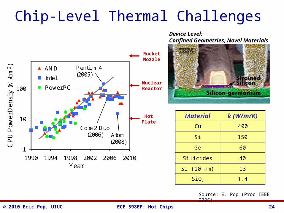
© 2010 Eric Pop, UIUC ECE 598EP: Hot Chips 24
1
10
100
1990 1994 1998 2002 2006 2010
AMD
Intel
Power PC
CP
U P
ower
Den
sity
(W
/cm
2)
Year
Pentium 4(2005)
Core 2 Duo(2006) Atom
(2008)
Chip-Level Thermal Challenges
Hot Plate
1.4SiO2
13Si (10 nm)
40Silicides
60Ge
150Si
k (W/m/K)Material
Device Level:Confined Geometries, Novel Materials
Source: E. Pop (Proc IEEE 2006)
400Cu
Nuclear Reactor
Rocket Nozzle

© 2010 Eric Pop, UIUC ECE 598EP: Hot Chips 25
Why (down)Scaling?To increase speed & complexity!$1000 buys:
Source: J. Welser, IBM
© 2010 Eric Pop, UIUC ECE 598EP: Hot Chips 26
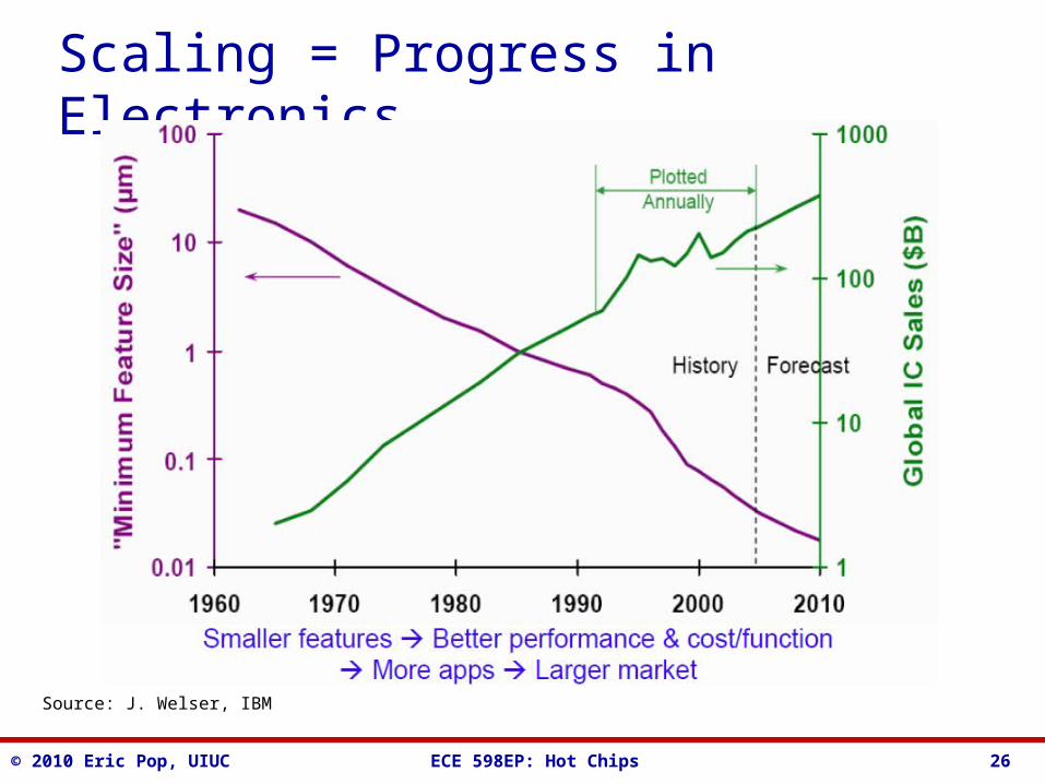
Scaling = Progress in Electronics
Source: J. Welser, IBM
© 2010 Eric Pop, UIUC ECE 598EP: Hot Chips 27
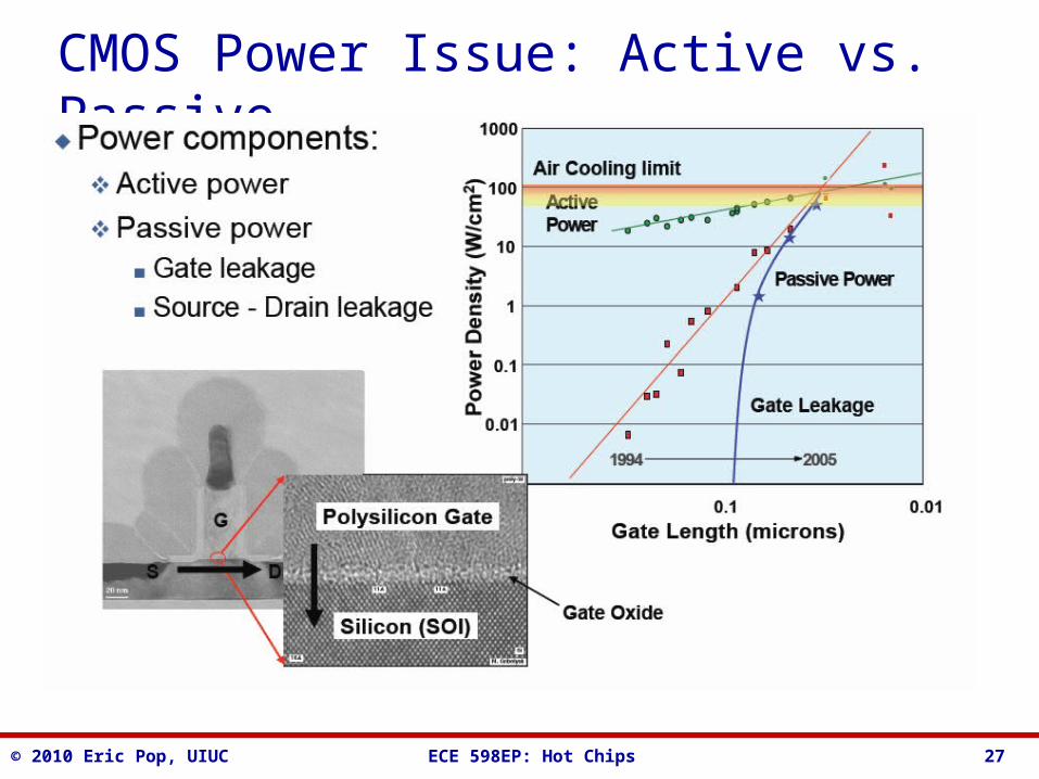
CMOS Power Issue: Active vs. Passive

© 2010 Eric Pop, UIUC ECE 598EP: Hot Chips 28
Power & Heat Limit Frequency Scaling
© 2010 Eric Pop, UIUC ECE 598EP: Hot Chips 29
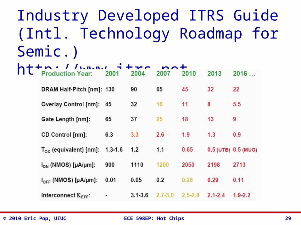
Industry Developed ITRS Guide(Intl. Technology Roadmap for Semic.)http://www.itrs.net

© 2010 Eric Pop, UIUC ECE 598EP: Hot Chips 30
Has This Ever Happened Before?
Source: J. Welser, IBM
© 2010 Eric Pop, UIUC ECE 598EP: Hot Chips 31
Implications for Nanoscale Circuits
© 2010 Eric Pop, UIUC ECE 598EP: Hot Chips 32
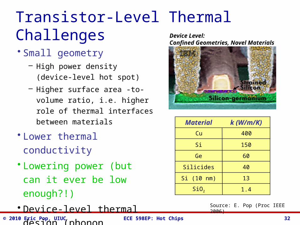
Transistor-Level Thermal Challenges
• Small geometry– High power density (device-level
hot spot)
– Higher surface area -to- volume
ratio, i.e. higher role of thermal
interfaces between materials
• Lower thermal conductivity
• Lowering power (but can it
ever be low enough?!)
• Device-level thermal design
(phonon engineering)
Source: E. Pop (Proc IEEE 2006)
1.4SiO2
13Si (10 nm)
40Silicides
60Ge
150Si
k (W/m/K)Material
Device Level:Confined Geometries, Novel Materials
400Cu
© 2010 Eric Pop, UIUC ECE 598EP: Hot Chips 33
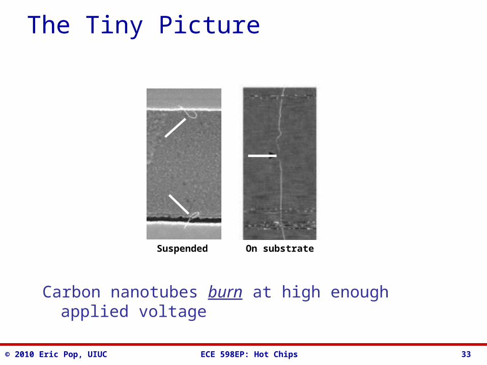
The Tiny Picture
Carbon nanotubes burn at high enough applied voltage
Suspended On substrate
© 2010 Eric Pop, UIUC ECE 598EP: Hot Chips 34
K of Nano{wires;layers}, RB of Interfaces
Thermal conductivity (K) of thin films and nanowires:– Decrease due to phonon confinement and boundary scattering
– Up to an order of magnitude decrease from bulk values
0
10
20
30
40
50
60
70
80
0 50 100 150d (nm)
k (W
/m/K
) Thin Si
SiGe NW
Si NW
Thin Ge
Data: Li (2003), Liu (2005); Model: Pop (2004)
Al/SiO2/SiGST/ZnS/SiO2
Bulk Si ~ 150, Ge ~ 60 W/m/K
Lyeo (2006)
SiO2
Al
RB
Thermal interface resistance ~ 10 nm SiO2

© 2010 Eric Pop, UIUC ECE 598EP: Hot Chips 35
0.1
1
10
100
1000
10000
100000
0.01 0.1 1 10L (mm)
RT
H (
K/m
W)
Thermal Resistance at Device Level
Cu
GST
SiO2
Si
Silicon-on-Insulator FET
Bulk FET
Cu Via
Phase-change Memory (PCM)
Single-wall nanotube SWNT
Data: Mautry (1990), Bunyan (1992), Su (1994), Lee (1995), Jenkins (1995), Tenbroek (1996), Jin (2001), Reyboz (2004), Javey (2004), Seidel (2004), Pop (2004-6), Maune (2006).
High thermal resistances:
• SWNT due to small thermal conductance (very small d ~ 2 nm)
• Others due to low thermal conductivity, decreasing dimensions, increased role of interfaces
Power input also matters:
• SWNT ~ 0.01-0.1 mW
• Others ~ 0.1-1 mW
© 2010 Eric Pop, UIUC ECE 598EP: Hot Chips 36
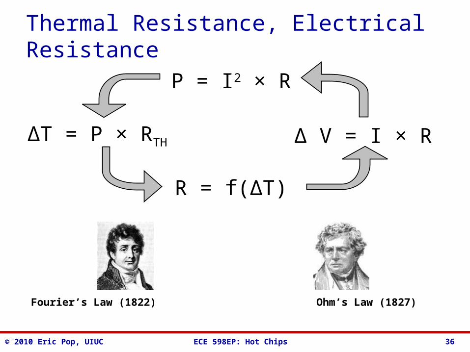
Thermal Resistance, Electrical Resistance
Ohm’s Law (1827)Fourier’s Law (1822)
∆ V = I × R∆T = P × RTH
P = I2 × R
R = f(∆T)

© 2010 Eric Pop, UIUC ECE 598EP: Hot Chips 37
This Heating Business is Not All Bad…
IF we can control it!

© 2010 Eric Pop, UIUC ECE 598EP: Hot Chips
Nanotubes in the Carbon WorldAllotropes of Carbon:
Diamond
Buckyball(C60)
Amorphous(soot)
Graphite (pencil lead)
Single-Walled Nanotube
38
© 2010 Eric Pop, UIUC ECE 598EP: Hot Chips
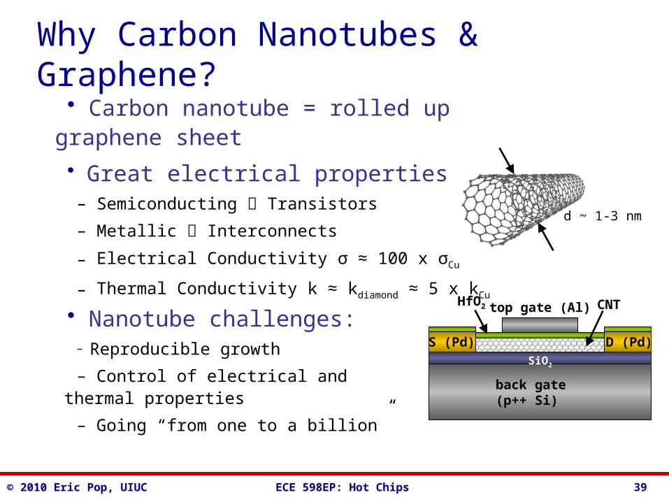
• Carbon nanotube = rolled up graphene sheet
• Great electrical properties– Semiconducting Transistors
– Metallic Interconnects
– Electrical Conductivity σ ≈ 100 x σCu
– Thermal Conductivity k ≈ kdiamond ≈ 5 x kCu
back gate(p++ Si)
HfO2
S (Pd) D (Pd)SiO2
top gate (Al) CNT
Why Carbon Nanotubes & Graphene?
d ~ 1-3 nm
• Nanotube challenges:– Reproducible growth
– Control of electrical and thermal properties
– Going “from one to a billion”
39

© 2010 Eric Pop, UIUC ECE 598EP: Hot Chips
Light Emission from Metallic SWNTs
• Joule-heated tubes emit light:– Comes from center, highly polarized– Emitted photons at higher energy than
applied bias (high energy tail)– World’s smallest light bulb?
D. Mann et al., Nature Nano 2, 33 (2007)
~ σT4
Polarization
Energy (eV)2.2
suspended
1
0
2
1.4 1.6 1.8
3
2.0
on substrate S
S
D
γ(a
.u.)
Vds = 1.4 V
Vds = 7 V
900 750 600Wavelength (nm)
angle0 90
γ(a
.u.)
1
0
-5
5
0
1 2
source
drain
Dis
tanc
e (m
m)
γ (a.u.)0
tren
ch
40
© 2010 Eric Pop, UIUC ECE 598EP: Hot Chips 41
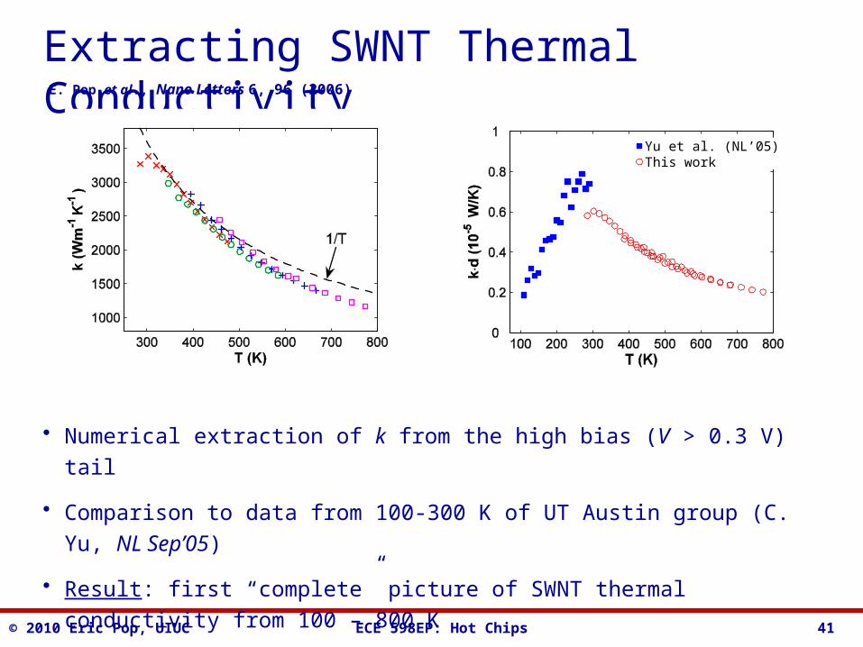
Extracting SWNT Thermal Conductivity
• Numerical extraction of k from the high bias (V > 0.3 V) tail
• Comparison to data from 100-300 K of UT Austin group (C. Yu, NL Sep’05)
• Result: first “complete” picture of SWNT thermal conductivity from 100 – 800 K
E. Pop et al., Nano Letters 6, 96 (2006)
Yu et al. (NL’05)This work
© 2010 Eric Pop, UIUC ECE 598EP: Hot Chips 42
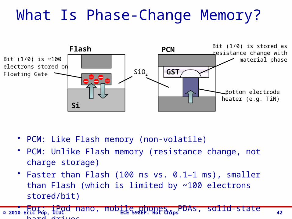
What Is Phase-Change Memory?
• PCM: Like Flash memory (non-volatile)• PCM: Unlike Flash memory (resistance change, not charge storage)• Faster than Flash (100 ns vs. 0.1–1 ms), smaller than Flash (which
is limited by ~100 electrons stored/bit)• For: iPod nano, mobile phones, PDAs, solid-state hard drives…
Si
GST
Flash PCMBit (1/0) is ~100electrons stored onFloating Gate
Bottom electrodeheater (e.g. TiN)
Bit (1/0) is stored asresistance change with
material phase
SiO2

© 2010 Eric Pop, UIUC ECE 598EP: Hot Chips 43
How Phase-Change Materials Work
• Based on Ge2Sb2Te5 reversible phase change
• Amorphous to Crystalline resistivity change > 100x
• Control phase transitions with pulsed Joule heating (~100 ns / 0.1 mA)
0 100 200 300 40010
2
103
104
105
106
107
108
Temperature (oC)
Res
istiv
ity (
m c
m)
Amorphous (a)
Cubic (fcc)
Hexagonal(hcp)
(a)
0 1 2 3 40
0.1
0.2
0.3
Voltage (V)
Cur
rent
(A
)
VTH
Data "0"low-R (fcc)
Data "1" high-R (a)
(b)
Curr
ent
(mA
)
© 2010 Eric Pop, UIUC ECE 598EP: Hot Chips 44
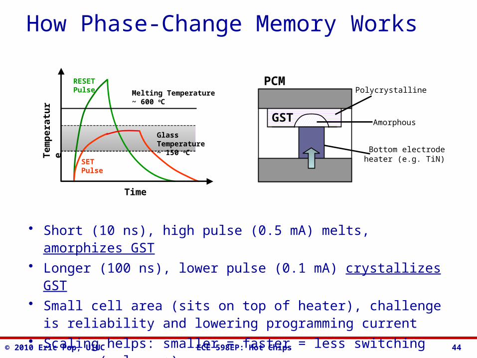
How Phase-Change Memory Works
• Short (10 ns), high pulse (0.5 mA) melts, amorphizes GST• Longer (100 ns), lower pulse (0.1 mA) crystallizes GST• Small cell area (sits on top of heater), challenge is reliability and
lowering programming current• Scaling helps: smaller = faster = less switching energy (volume ↓)
GST
PCM
Amorphous
PolycrystallineRESETPulse
Time
SETPulse
Glass Temperature ~ 150 oC
Melting Temperature~ 600 oC
Tem
per
atu
re
Bottom electrodeheater (e.g. TiN)
© 2010 Eric Pop, UIUC ECE 598EP: Hot Chips 45
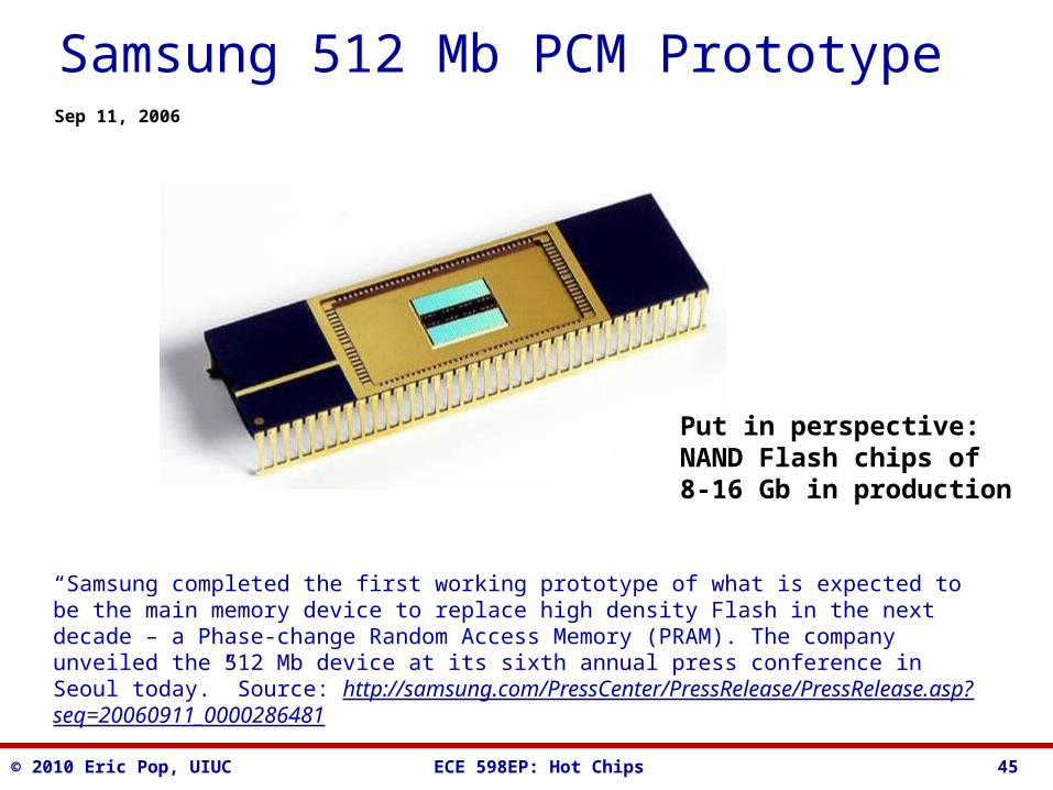
Samsung 512 Mb PCM Prototype
“Samsung completed the first working prototype of what is expected to be the main memory device to replace high density Flash in the next decade – a Phase-change Random Access Memory (PRAM). The company unveiled the 512 Mb device at its sixth annual press conference in Seoul today.” Source: http://samsung.com/PressCenter/PressRelease/PressRelease.asp?seq=20060911_0000286481
Sep 11, 2006
Put in perspective:NAND Flash chips of8-16 Gb in production
© 2010 Eric Pop, UIUC ECE 598EP: Hot Chips 46
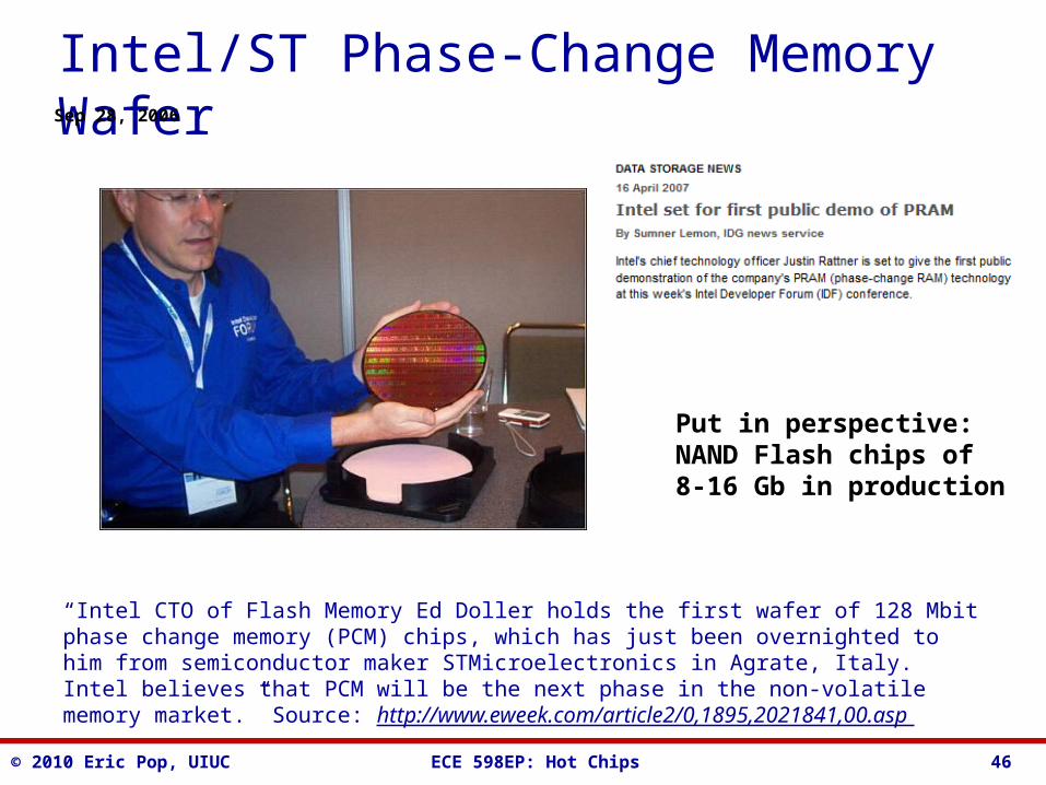
Intel/ST Phase-Change Memory Wafer
“Intel CTO of Flash Memory Ed Doller holds the first wafer of 128 Mbit phase change memory (PCM) chips, which has just been overnighted to him from semiconductor maker STMicroelectronics in Agrate, Italy. Intel believes that PCM will be the next phase in the non-volatile memory market.” Source: http://www.eweek.com/article2/0,1895,2021841,00.asp
Sep 28, 2006
Put in perspective:NAND Flash chips of8-16 Gb in production


