download abstract book - ::::::iedms 2014::::::
TRANSCRIPT

Table of Contents Map ............................................................................................................................................ 1
Schedule .................................................................................................................................... 2
Organizers ................................................................................................................................. 4
Sponsors .................................................................................................................................... 5
General Information .................................................................................................................. 6
General Program Information.................................................................................................... 8
Speakers ................................................................................................................................... 9
Plenary Session ...................................................................................................................... 13
Oral Session ............................................................................................................................. 20
Poster Session .......................................................................................................................... 68

1
Map
2 F
1 F
Map

2
Schedule
Schedule
2

3
3

4
Organizers
Co-organizers

5
Sponsors

6
General Information
Organizer:
Electronics Devices and Materials Association (EDMA)
Ministry of Science and Technology (MOST)
National Dong Hwa University (NDHU)
Honorary Conference Chair:
Maw-Kuen Wu, President, NDHU
Conference Chair (List by Alphabet):
Ro-Min Weng, NDHU (Chair)
Huang-Chung Cheng, EDMA (Co-Chair)
Tai-Ping Sun, EDMA (Co-Chair)
Tseung-Yuen Tseng, MOST (Co-Chair)
International Advisory Committee (List by Alphabet):
Hiroshi Ishiwara, Tokyo Institute of Technology, Japan
Juin J. Liou, University of Central, USA
Weiguang Zhu, Nanyang Technological University, Singapore
Organizing Committee (List by Alphabet):
Chun-Chieh Lin, NDHU (Chair)
Chia-Hua Huang, NDHU
Chu-Hsuan Lin, NDHU
Chuan-Hsi Liu, NTNU
Keng-Ming Liu, NDHU
Mei-Hsin Chen, NDHU
Ying-Chieh Ho, NDHU
Yu-Shyan Lin, NDHU
Program Committee (List by Alphabet):
Chu-Hsuan Lin, NDHU (Chair)
Bing-Yue Tsui, NCTU (Co-Chair)
Chung-Chih Wu, NTU (Co-Chair)
Horng-Chih Lin, NCTU (Co-Chair)
Wei-Chou Hsu, NCKU (Co-Chair)

7
Bae-Heng Tseng, NSYSU
Chao-Hsin Chien, NCTU
Chao-Sung Lai, CGU
Cheewee Liu, NTU
Chen-Hsin Lien, NTHU
Chia-Hua Huang, NDHU
Chuan-Hsi Liu, NTNU
Chun-Chieh Lin, NDHU
Chun-Yu Lin, NTNU
Edward Yi Chang, NCTU
Hao-Hsiung Lin, NTU
Jeng-Tzong Sheu, NCTU
Jenn-Gwo Hwu, NTU
Jer-Chyi Wang, CGU
Jr-Hau He, NTU
Keng-Ming Liu, NDHU
Kuan-Neng Chen, NCTU
Kuei-Shu Chang-Liao, NTHU
Li-Yin Chen, NSYSU
Mei-Hsin Chen, NDHU
Meng-Chyi Wu, NTHU
Pei-Wen Li, NCU
Shoou-Jinn Chang, NCKU
Shu-Tong Chang, NCHU
Tsong-Sheng Lay, NCHU
Tuo-Hung Hou, NCTU
Wen-Kuan Yeh, NDL
Yeong-Her Wang, NCKU
Yeu-Long Jiang, NCHU
Ying-Chieh Ho, NDHU
You-Lin Wu, NCNU
Yu-Shyan Lin, NDHU
Yue-Ming Hsin, NCU
Secretariat:
Min-Lin Chen, NDHU
S.-F. Lo, EMDA

8
General Program Information
2014 International Electron Devices and Materials Symposium (IEDMS 2014) will be
held on Nov. 20-21, 2014, at Fullon Hotel, Hualien, Taiwan. The IEDMS 2014 is
intended to provide a common forum for researchers, scientists, engineers, and
practitioners throughout the world to present their latest research findings, ideas,
developments, and applications in the area of semiconductor materials and devices.
Topics of interest will include, but are not limited to, the following:
A.Compound Semiconductor Materials, Electronic and Photonic Devices
B.Sustainable Energy Devices and Materials
C.Integrated Circuits and Packaging Technologies
D.Nano Devices and Materials, Memories, Displays, and Sensors
Important Dates:
Abstract Submission: Aug. 31, 2014
Notification of Acceptance: Oct. 01, 2014
Early-Bird Registration Deadline: Oct. 31, 2014
Special Issue Deadline: Nov. 19, 2014
For Invited Talks
Time for the invited talk is 30 minutes, including last 3 minutes for discussion.
For Oral Papers
Time allotted for your presentation is 15 minutes, including last 3 minutes for
discussion.
Please report to the Session Chair and upload your PowerPoint file to the
Notebook computer in the session room at least 10 minutes before the session
begins.
For Poster Papers
The size of a poster board is 90 cm (width) x 180 cm (height). The recommended
size of your poster is A0 (84.1 cm (width) x 118.9 cm (height)).
Free WiFi Access
WiFi: Fullon_Hotels HL
Password: 8888888888

9
Speakers (List by Session Schedule)
Plenary Speakers
Prof. Jenn-Gwo Hwu 胡振國教授
National Taiwan University, Taiwan
Title: Nanoscale Oxide Engineering on Si Substrate
Time: Nov. 20 09:20-10:00 (Room B)
Prof. Juin J. Liou
University of Central Florida, USA
Title: Prospect and Outlook of Electrostatic Discharge (ESD)
Protection in Emerging Technologies
Time: Nov. 20 10:30-11:10 (Room B)
Dr. Shinji Yuasa
National Institute of Advanced Industrial Science and Technology
(AIST), Japan
Title: Perspectives on Spintronics and MRAM Technologies
Time: Nov. 20 11:10-11:50 (Room B)
Invited Speakers
Prof. Steve S. Chung 莊紹勳教授
National Chiao Tung University, Taiwan
Title: The Experimental Observation of the Dopant Fluctuations
in Trigate FinFETs
Time: Nov. 20 13:30-14:00 (Room A)
10
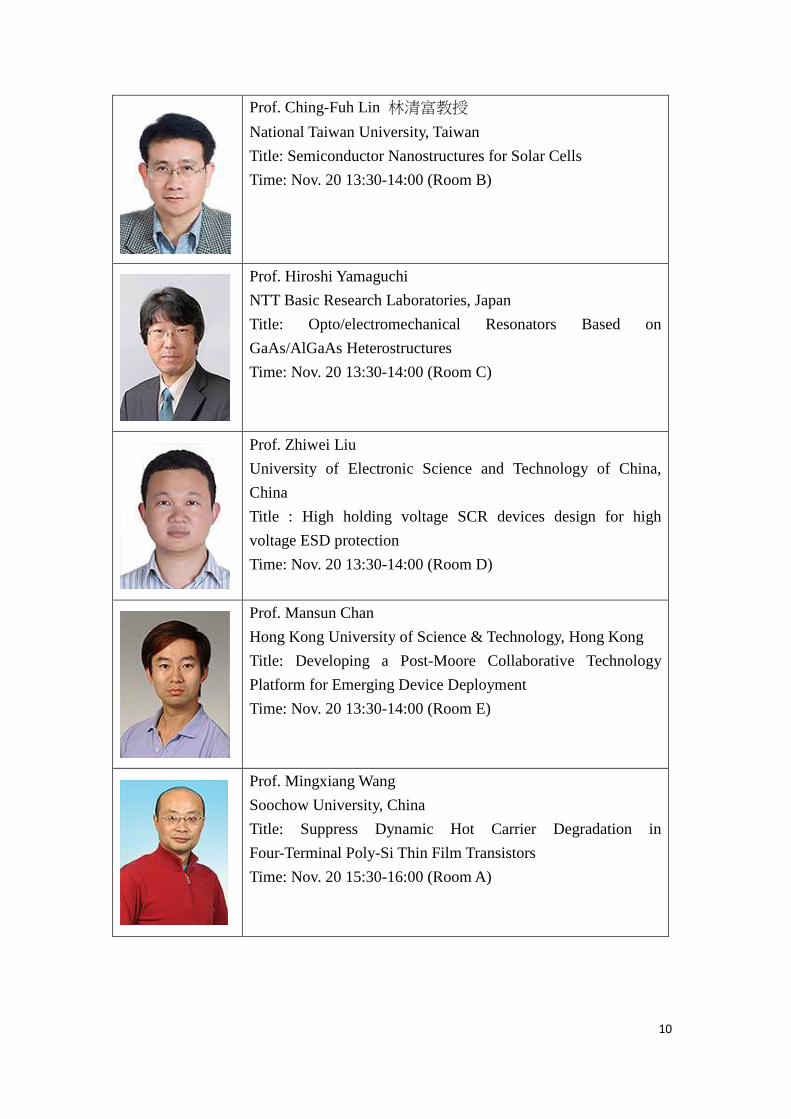
Prof. Ching-Fuh Lin 林清富教授
National Taiwan University, Taiwan
Title: Semiconductor Nanostructures for Solar Cells
Time: Nov. 20 13:30-14:00 (Room B)
Prof. Hiroshi Yamaguchi
NTT Basic Research Laboratories, Japan
Title: Opto/electromechanical Resonators Based on
GaAs/AlGaAs Heterostructures
Time: Nov. 20 13:30-14:00 (Room C)
Prof. Zhiwei Liu
University of Electronic Science and Technology of China,
China
Title : High holding voltage SCR devices design for high
voltage ESD protection
Time: Nov. 20 13:30-14:00 (Room D)
Prof. Mansun Chan
Hong Kong University of Science & Technology, Hong Kong
Title: Developing a Post-Moore Collaborative Technology
Platform for Emerging Device Deployment
Time: Nov. 20 13:30-14:00 (Room E)
Prof. Mingxiang Wang
Soochow University, China
Title: Suppress Dynamic Hot Carrier Degradation in
Four-Terminal Poly-Si Thin Film Transistors
Time: Nov. 20 15:30-16:00 (Room A)

11
Prof. Cher-Ming Tan 陳始明教授
Chang Gung University, Taiwan
Title: Exploring the Humidity Effect on the Reliability of High
Power LEDs
Time: Nov. 20 15:30-16:00 (Room B)
Prof. Ru Huang
Peking University, China
Title: Junction Engineering of Tunnel FETs for Steep Switching
and Improved Noise Behavior
Time: Nov. 20 15:30-16:00 (Room C)
Prof. Shun-Ichiro Ohmi
Tokyo Institute of Technology, Japan
Title: Room Temperature Fabrication of Pentacene-Based
OFETs with Hf-Based High-k Gate Insulator for Low Voltage
Operation
Time: Nov. 20 15:30-16:00 (Room D)
Prof. Kin-Leong Pey
Singapore University of Technology and Design, Singapore
Title: Filamentary Switching with Semiconducting Bottom
Electrode – Physical Insight and Advantages
Time: Nov. 20 15:30-16:00 (Room E)
Prof. Horng-Chih Lin 林鴻志教授
National Chiao Tung University, Taiwan
Title: Fabrication of Thin-Film Transistors/Inverters with Film
Profile Engineering
Time: Nov. 21 10:30-11:00 (Room A)
Prof. Tzung-Fang Guo 郭宗枋教授
National Cheng Kung University, Taiwan
Title: Nickel oxide p-type electrode interlayer in CH3NH3PbI3
perovskite/fullerene planar-heterojunction hybrid solar cells
Time: Nov. 21 10:30-11:00 (Room B)

12
Prof. Pei-Wen Li 李佩雯教授
National Central University, Taiwan
Title: Designer Germanium Quantum-Dot for Nanoeletronics
and Nanophotonics Devices
Time: Nov. 21 10:30-11:00 (Room C)
Prof. Te-Kung Chiang 江德光教授
National University of Kaohsiung, Taiwan
Title: A New Quasi-3D Compact Threshold Voltage Model for
Pi-Gate (PG) MOSFETs with the Interface Trapped Charges
Time: Nov. 21 10:30-11:00 (Room D)
Dr. ChiaHua Ho 何家驊博士
Winbond Electronics Corporation, Taiwan
Title: Overview of Emerging Non-Volatile Memories
Time: Nov. 21 10:30-11:00 (Room E)

13
Plenary Session 1
Nov. 20, 09:20-10:00, 2F Room B
Prof. Jenn-Gwo Hwu
Distinguished Professor, National Taiwan University, Taiwan
Presentation Title: Nanoscale Oxide Engineering on Si Substrate
Authors: Po-Hao Tseng, Yen-Kai Lin, Han-Wei Lu, Yu-Ching Liao, and Jenn-Gwo
Hwu*
Abstract:
Anodization technique was introduced for the oxide formation in nanoscale
device application. There are two parts in this talk. Single crystal Si nanowires with
dimension down to sub-10 nm can be formed by long time anodization. Several new
phenomena were presented. Anodization with suitable condition can also form various
oxide thicknesses on single wafer. It is useful to grow ultra-thin oxide with thickness
smaller than 3 nm. The MOS structures with various oxide thicknesses will be
characterized in the view point of I-V and C-V. There are several fundamental
differences between MOS(p) and MOS(n) structures. The current in inversion
becomes saturated when the oxide is thin enough. The saturation behavior is sensitive
to temperature, illumination, and charge trapping. Therefore, valuable applications of
nanoscale MOS devices are achievable. The physics left behind is of importance for
nanoscale study.
Biography
Jenn-Gwo Hwu was born in Tainan, Taiwan, Republic of china, on August 29,
1955. He received the B.S. degree in electronic engineering from National
Chiao-Tung University, Republic of China, in 1977 and the M.S. and Ph.D. degrees in
electrical engineering from National Taiwan University, Republic of China, in 1979

14
and 1985, respectively.
He joined the faculty of National Taiwan University in 1981. Presently, he is a
Professor in the Department of Electrical Engineering and the Graduate Institute of
Electronics Engineering, National Taiwan University. From 1997 to 1998, he was the
vice chairman of the Department of Electrical Engineering, National Taiwan
University. From February 2004 to January 2006, he was invited as the Dean of the
College of Electrical Engineering and Computer Science, National United University,
Miaoli, Taiwan, Republic of China. From December 2005 to December 2008, he was
invited as the Coordinator of Micro-Electronics Engineering Program, Department of
Engineering and Applied Sciences, National Science Council, Taiwan, Republic of
China. On August 2006, he was appointed as the Distinguished Professor of National
Taiwan University. And from August 2007 to July 2010, he was appointed as the
chairperson of the Department of Electrical Engineering, National Taiwan University.
His research work is mainly on ultra-thin gate oxide and its related Si MOS devices.
He has experience in teaching the courses of Circuits, Electronics, Solid-State
Electronics, Semiconductor Engineering, MOS Capacitor Devices, Radiation Effects
on MOS System, and Special Topic on Oxide Reliability.
He was qualified to be a licensed Professional and Technical Engineer on
Electrical and Electronics Engineering, R.O.C., in 1978 and 1980, respectively. He
was honored as the owner of Outstanding Teaching Award in 1991 by The Ministry of
Education and in 1987, 2003, and 2008 by National Taiwan University. He was also
the owner of Excellent Teaching Award in 1988, 1989, 1990, 1991, and 1993 by the
College of Engineering, National Taiwan University, and in 1999, 2000, and 2002 by
National Taiwan University. In 1999, he was the recipient of Jan Ten-You Paper
Award by The Chinese Institute of Engineering, R.O.C. In 2005, he was the recipient
of Scientific Paper Award by Far Eastern Y.Z.Hsu Science and Technology Memory
Foundation, Taiwan, R.O.C. In 2012, he was awarded the Himax Chair Professorship
at National Taiwan University.
Major Research Areas
Si MOS Devices/Ultra-thin Gate Oxide Processes/Novel Si-based Devices/Rapid
Thermal Processing-RTP /Uniformity Analysis and Stress Control/Si MOS Solar Cell
and Photo Sensors

15
Plenary Session 2
Nov. 20, 10:30-11:10, 2F Room B
Prof. Juin J. Liou
Lockheed Martin St. Laurent Professor of Engineering, School of EECS, University
of Central Florida
Presentation Title: Prospect and Outlook of Electrostatic Discharge (ESD)
Protection in Emerging Technologies
Author: Juin J. Liou
Abstract:
Electrostatic discharge (ESD) is a process in which a finite amount of charge is
transferred from one object (i.e., human body) to the other (i.e., microchip). This
process can result in a very high current passing through the object within a very short
period of time [1-2]. When a microchip or electronic system is subject to an ESD
event, the huge ESD-induced current can likely damage the microchip and cause
malfunction to the electronic system if the heat generated in the object cannot be
dissipated quickly enough. It is estimated that about 35% of all damaged microchips
are ESD related, resulting in a revenue loss of several hundred million dollars in the
global semiconductor industry every year [3]. The continuing diminishing in the size
of MOS devices makes the ESD-induced failures even more prominent, and one can
predict with certainty that the availability of effective and robust ESD protection
solutions will become a critical component to the successful development of the
CMOS-based integrated circuits.
Advancement of low-voltage electronics has been benefitted largely by the continue
scaling of CMOS technology, which is now reaching an astonishing milestone of
22-nm node. Beyond that, several new features will need to be implemented to enable
the continuation of CMOS miniaturization, including the high-k dielectric, metal gate,
multiple gate, etc. A noteworthy future CMOS development is the Si nanowire

16
technology. It has the advantages of a superior gate control, excellent on-current vs.
off-current ratio, very low power consumption, and extremely high cutoff frequency.
The ESD protection issues of such a technology are still largely unknown at this time
and need to be resolved urgently before the technology can be commercialized in the
consumer market in about 3-4 years [4]. On the other hand, high-voltage electronics,
such as those used in the automobiles, are increasingly important and popular. These
SoC’s are typically fabricated in the bipolar/CMOS/DMOS (BCD) process, and such
applications imposed additional challenges on the design and implementation of
high-voltage ESD protection solutions [5].
Some comments on the ESD standards are in order. Human body model is a mature,
well-understood ESD model for simulating charge transfer from a person's finger to
an electronic component. However, recent industry data indicates that the HBM rarely
simulates real-world ESD failures. Latest generation package styles such as mBGAs,
SOTs, SC70s, & CSPs with mm-range dimensions are often effectively too small for
people to handle with fingers. Even in cases of relatively large components, most
high-volume component and board manufacturing uses automated equipment, so
humans rarely touch the components. Charged device model can more successfully
replicate in-house and customer IC failures at the component level [6].
In the presentation, the fundamentals of ESD, including its mechanisms, standards,
protection principles, and testing will first be introduced. This is followed by the
exploration and evaluation of ESD protection solutions in emerging Si nanowire,
organic, and GaN technologies.
Acknowledgements—This work was supported financially or in-kind by Analog
Devices Inc., USA, Intersil Corp., USA, National Semiconductor Corp., USA,
National Center for Nanomaterials Technology, Korea, Institute of Microelectronics,
Singapore, and Ministry of Education, China.
REFERENCES
[1] J. Vinson, G. Croft, J. Bernier, and J. J. Liou, Electrostatic Discharge Analysis
and Design Handbook, Kluwer Academic Publishers, Boston, 2002.
[2] J. Vinson and J. J. Liou, “Electrostatic discharge in semiconductor devices:
protection techniques,” (Invited Paper) Proceedings of the IEEE, vol. 88, pp.
1878-1900, Dec. 2000.
[3] M. Brandt and S. Halperin, “What does ESD really cost?”, Circuits Assembly

17
Magazine, June 1, 2003.
[4] W. Liu, J. J. Liou, et al., “Electrostatic discharge (ESD) robustness of Si
nanowire field-effect transistors,” IEEE Electron Device Letters, vol. 30, pp. 969-971,
Sept. 2009.
[5] Z. Liu, J. J. Liou, and J. Vinson, “Novel silicon controlled rectifier for
high-voltage ESD applications,” IEEE Electron Device Letters, vol. 29, pp. 753-755,
July 2008.
[6] Z. Gan, W. Wong, and J. J. Liou, Semiconductor Process Reliability: in Practice,
McGraw-Hill, New York, 2012.
Honor and Awards
Dr. Liou has been awarded 8 U.S. patents, and has published 10 books, 2 book
chapter, more than 260 journal papers (including 16 invited articles), and more than
220 papers (including more than 90 keynote/invited papers) in international and
national conference proceedings. He has been awarded over $12.0 million of research
contracts and grants from federal agencies, state government, and industry, and has
held consulting positions with research laboratories and companies in the United
States, China, Japan, Taiwan, and Singapore.
Dr. Liou was awarded the UCF Pegasus Distinguished Professor in 2009 – the
highest honor bestowed to a faculty member at UCF, UCF Distinguished Researcher
Award in 1992, 1998, 2002, and 2009, and IEEE Joseph M. Biedenbach Outstanding
Engineering Educator Award in 2004. His other honors are Fellow of IEEE, Fellow of
IET, and Chang Jiang Endowed Professor of Ministry of Education, China – the
highest honorary professorship in China.
Dr. Liou has served as the IEEE EDS Vice-President of Regions/Chapters, IEEE
EDS Treasurer, IEEE EDS Finance Committee Chair, Member of IEEE EDS Board of
Governors, and Member of IEEE EDS Educational Activities Committee.
18
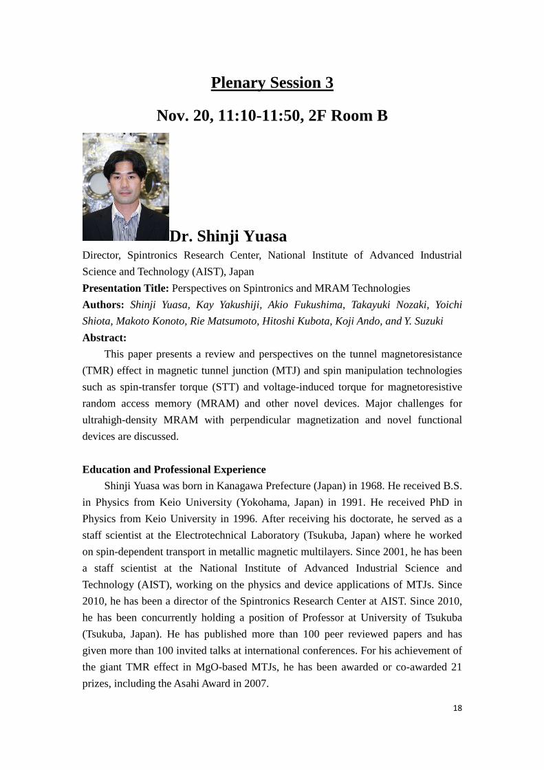
Plenary Session 3
Nov. 20, 11:10-11:50, 2F Room B
Dr. Shinji Yuasa
Director, Spintronics Research Center, National Institute of Advanced Industrial
Science and Technology (AIST), Japan
Presentation Title: Perspectives on Spintronics and MRAM Technologies
Authors: Shinji Yuasa, Kay Yakushiji, Akio Fukushima, Takayuki Nozaki, Yoichi
Shiota, Makoto Konoto, Rie Matsumoto, Hitoshi Kubota, Koji Ando, and Y. Suzuki
Abstract:
This paper presents a review and perspectives on the tunnel magnetoresistance
(TMR) effect in magnetic tunnel junction (MTJ) and spin manipulation technologies
such as spin-transfer torque (STT) and voltage-induced torque for magnetoresistive
random access memory (MRAM) and other novel devices. Major challenges for
ultrahigh-density MRAM with perpendicular magnetization and novel functional
devices are discussed.
Education and Professional Experience
Shinji Yuasa was born in Kanagawa Prefecture (Japan) in 1968. He received B.S.
in Physics from Keio University (Yokohama, Japan) in 1991. He received PhD in
Physics from Keio University in 1996. After receiving his doctorate, he served as a
staff scientist at the Electrotechnical Laboratory (Tsukuba, Japan) where he worked
on spin-dependent transport in metallic magnetic multilayers. Since 2001, he has been
a staff scientist at the National Institute of Advanced Industrial Science and
Technology (AIST), working on the physics and device applications of MTJs. Since
2010, he has been a director of the Spintronics Research Center at AIST. Since 2010,
he has been concurrently holding a position of Professor at University of Tsukuba
(Tsukuba, Japan). He has published more than 100 peer reviewed papers and has
given more than 100 invited talks at international conferences. For his achievement of
the giant TMR effect in MgO-based MTJs, he has been awarded or co-awarded 21
prizes, including the Asahi Award in 2007.
19
Research Field
His research field includes magnetism, magnetic materials, thin films and
multilayers, and spintronics. For the last decade, he has been mainly working on
tunnel magnetoresistance and spin-transfer torque in magnetic tunnel junctions
(MTJs), especially MgO-based MTJs. He is interested in both the basic physics and
device applications of MTJs.
Contribution to Society
Shinji Yuasa served as an Editor of Magnetics Society of Japan from 2001 to
2010. He also served as a member of Program Committees for 19th International
Colloquium on Magnetic Films and Surfaces (ICMFS 2006), 55th Annual Conference
on Magnetism and Magnetic Materials (MMM 2010), and IEEE International
Magnetics Conference (Intermag 2011). He was a Vice-chair of Gordon Research
Conference on Magnetic Nanostructure 2010 and a member of International Advisory
Committee for The IEEE 7th International Symposium on Metallic Multilayers (MML
2010). He is now serving as a Program Co-chair for the 2013 Joint MMM/Intermag
Conference, a member of the Advisory Committee for the MMM Conference, and a
member of Program Committee for 21st International Colloquium on Magnetic Films
and Surfaces (ICMFS 2012). He is an Editor of Applied Physics Express / Jpn. J. Appl.
Phys. since 2009. He has also been assigned as the IEEE Distinguished Lecturer for
2012.
Recognition
He has been awarded or co-awarded the following scientific prizes :
-IEEE Distinguished Lecturer for 2012
-Japan Society for the Promotion of Science (JSPS) Prize (2010)
-Tsukuba Prize (2010)
-Inoue Harushige Prize (2009) (together with Canon-Anelva Corp.)
-The Prime Minister Award of Japan (2008) (together with D. D. Djayaprawira and Y.
Suzuki)
-Asahi Award (2007) (together with T. Miyazaki)
-IBM Japan Prize (2007)
-Tokyo Techno Forum 21 Gold Medal (2006)
-Marubun Science Prize (2006)
-The Japan Society of Applied Physics (JSAP) Best Paper Award (2005)
-Ichimura Science Prize (2004)
-10 other prizes.
20
Oral Session
Session 1: FinFET (November 20)
Room A
Chair: Prof. Jenn-Gwo Hwu, Department of Electrical Engineering, National Taiwan
University, Taiwan
13:30~14:00 (Invited) The Experimental Observation of the Dopant
Fluctuations in Trigate FinFETs Steve S Chung
Department of Electronics Engineering, National Chiao Tung University, Taiwan
The random dopant fluctuation is one of the most important issues
for the 16nm and beyond CMOS technologies with trigate FinFET
structure in terms of the device architecture and manufacturing. This
paper will demonstrate the methodology to understand the dopant
fluctuation via a purely experimental approach. It will be
demonstrated in advanced trigate FinFET devices. The discrete
dopant distribution along the channel direction can be determined.
Boron clustering effect in nMOSFETs can be reasonably explained
which results in a larger Vth variation, in comparison to that of
pMOSFETs. Moreover, experiments have been extended to the
advanced trigate CMOS devices. The sidewall roughness and the
LER(Line edge roughness) in trigate have also been examined. This
approach provides a good monitor of the quality of 3D gate structure
and the random dopant fluctuation (RDF) of advanced trigate
devices.
14:00~14:15 #1209 Simulation Study of Gate and Fin Line Edge Roughness
Effects on 14 nm Inversion-Mode and Junctionless FinFETs
Li-Syun Yang, and Keng-Ming Liu
Department of Electronical Engineering, National Dong Hwa University, Taiwan
In this paper we simulated the gate and fin line edge roughness
(LER) effects on the 14 nm inversion-mode (IM) and junctionless
(JL) FinFETs. Different rms amplitudes of gate and fin LER were
simulated to examine their effects on the device characteristics. The
simulation results show that the gate LER effects are more
significant than the fin LER effects except the on-state current. We
also found that, as far as LER is concerned, JL FinFETs are more
21
vulnerable than the IM FinFETs except that the on-state current
fluctuation of the IM FinFETs is larger than that of the JL FinFETs.
14:15~14:30 #1212 Vertically Stacked Nanowire Transistors Using
Low-Temperature Microwave Annealing Ming-Kun Huang1, Wen-Fa Wu2, and Chun-Hsing Shih1 1Department of Electrical Engineering, National Chi Nan University, Taiwan 2National Nano Device Laboratories, Taiwan
Thermal budget is one of the major concerns to fabricate
three-dimensional nanowire transistors. This work uses
low-temperature microwave annealing to fabricate vertically stacked
gate-all-around nanowire transistors. A microwave power of 400%
and a processing time of 150s were used in post-implantation
annealing to minimize thermal energy while retaining sufficient
activation. The vertically stacked nanowire devices show nearly
doubled drain currents compared to their non-stacked counterparts.
14:30~14:45 #1308 Fabrication and Characterization of Al2O3/InAs Fin
Field-Effect Transistors Cheng-Hsuan Hsieh1, Wei-Jen Hsueh1 and Jen-Inn Chyi1,2,3,4,* 1Department of Electrical Engineering, National Central University, Taiwan 2Optical Sciences Center, National Central University, Taiwan 3National Applied
Research Laboratories, Taiwan 4Research Center for Applied Science, Academia
Sinica, Taiwan
Al 2O3/n-InAs Fin Field-Effect Transistors (FinFETs) with gate
length of 0.5 µm, source to drain separation of 2 µm and effective
fin width of 60 nm are demonstrated in this work. The FinFETs
exhibit a maximum drain current density (IDmax) of 119 µA/µm, a
maximum transconductance (Gmmax) of 77.2 µS/µm, a threshold
voltage of -2.37 V, a drain current on-off ratio of 136, and a
subthreshold swing of 524 mV/decade.
14:45~15:00 #1332 Effect of Channel-Fin Width and Angle on Optimal
Characteristic of Trapezoidal-Shaped Bulk FinFET Devices Li-Wen Chen1,2 and Yiming Li1,2,3,* 1Parallel and Scientific Computing Laboratory, National Chiao Tung University,
Taiwan 2Institute of Communications Engineering, National Chiao Tung
University, Taiwan 3Department of Electrical and Computer Engineering, National
Chiao Tung University, Taiwan
In this work, we study the 16-nm-gate trapezoidal HKMG bulk
FinFET devices and its implication on static random access memory
22
(SRAM) cell. Electrical characteristic, short channel effect, and
transfer property are assessed considering different silicon fin
thickness and angle employed a calibrated 3D device-circuit coupled
simulation technique. To meet the given specification: the
subthreshold swing (SS) < 72 mV/dec, the drain induced barrier
lowing (DIBL) < 65 mV/V, and static noise margin (SNM) of 6-T
SRAM > 85 mV, optimal critical angles of channel fin: 90o, 80o, and
76o are found for the fin widths: 16, 12, and 8 nm, respectively.
Session 2: Solar Cell I (November 20)
Room B
Chair: Wei-Sheng Liu, Department of Photonics Engineering, Yuan Ze University,
Taiwan
13:30~14:00 (Invited) Semiconductor Nanostructures for Solar Cells
Ching-Fuh Lin, Hong-Jhang Syu, and Thiyagu Subramani
Director of i-PARC and Professor of GIPO, GIEE, & EE Dept., National Taiwan
University
Solar energy is one of the good choices to replace conventional
fossil energies due to its abundance. However, the limited solar
intensity leads to a need of huge areas to harvest sufficient sunlight.
Therefore, low cost and high productivity are very important for
photovoltaics. Here we report the low-cost approaches to fabricate
semiconductor nanostructures for solar cells. First, we use organic
materials for light absorption and combine them with ZnO nanorods
that are grown using solution process. This platform with ZnO
nanorods can lead to PCE of more than 7 % for several organic
polymers. The best one is over 8%. Second, Si nanowires are
combined with the organic materials to form p-n junction. The
fabrication can also be fabricated using low-cost solution processes.
The device so far demonstrated PCE near 13 %. We also developed
a technique based on chemical etching nano-structures to form very
thin single-crystal Si films. The thickness could be from around 5
µm to 20 µm. The rest of the Si wafer can be reused to form more
single crystalline Si thin films, so the material cost can be reduced to
only 1/10 or less. Details will be discussed.
14:00~14:15 #1134 Fabrication of Deformed TiO2 Aggregate and Application
as Photoanode in Dye Sensitized Solar Cells Kuo-Che Tseng1, Hsueh-Tao Chou1, Ho-Chun Hsu2
23
1Department of Electronic Engineering, National Yunlin University of Science
and Technology, Taiwan 2Graduate School of Engineering Science and
Technology, National Yunlin University of Science and Technology, Taiwan.
The deformed TiO2 aggregate was synthesized by two-step
method with tri-block copolymer as template. The photovoltaic
properties of deformed TiO2 aggregate as photoanode in
dye-sensitized solar cells (DSSCs) were investigated. The
photoanode of deformed TiO2 aggregate possesses enhanced light
harvesting and a larger amount of dye loading. An overall
conversion efficiency of deformed TiO2 aggregate as photoanode is
2.64% under illumination of simulated AM 1.5G solar light (100
mWcm-2). However, the efficiency is lower than the P25
nanoparticles as photoanode (3.1%). The electrochemical impedance
spectroscopy (EIS) was performed to investigate electronic
processes in DSSCs, and the results showed that deformed TiO2 aggregate possesses a lot of grain boundaries to hinder the electron
transport.
14:15~14:30 #1213 P-layer Properties on the Performance of a-Si:H p-i-n
Solar Cells Yo-Jin Yang, Yeu-Long Jiang*, and Yi-Chih Kuo
Graduate Institute of Optoelectronic Engineering and Department of Electrical
Engineering, National Chung Hsing University, Taiwan
Various p-layers of hydrogenated amorphous silicon (a-Si:H)
p-i-n solar cells were fabricated by plasma-enhanced chemical vapor
deposition (PECVD) to investigate the effects of the bandgap (Eg),
the activation energy (Ea) of p-layer and the double p-layers
structure on the performance of solar cells. Increasing the methane
gas flow ratio (Cx) could raise the Eg of p-layer, resulting in the
decrease of the light absorption in p-layer, and generating more
electron-hole pairs in the i-layer. The open-circuit voltage (Voc) and
the short-circuit current density (Jsc) were increased. However, high
bandgap offset at the p/i interface and high energy barrier at the
TCO/p interface increased the series resistance (Rs), and reduced the
fill factor (FF). Modulation the methane and diborane gas flow ratio
(Cx(By)) to obtain the p- layers with the same Eg but change their Ea,
the results showed that low Ea reduced the Rs, resulting in the
increase of FF. Adding a low-Eg (PL) p-layer between the TCO and
a high-Eg (PH) p-layer to form a double p-layers could increase the

24
conductivity and reduce Rs, resulting in increase of FF and the
efficiency (η) of a- Si:H p-i-n solar cells.
14:30~14:45 #1310 Medium Bandgap Conjugated Polymer Merging a
Fluorinated Quinoxaline Moiety for Efficient and Ai r-Stable
Solar Cells Wei-Hsuan Tseng1, Jung-Hung Chang1, Yun-Chen Chien2, Chih-I Wu1* 1Department of Electrical Engineering and Graduate Institute of Electrooptical
Engineering, National Taiwan University, Taiwan, 2Department of Chemistry,
National Taiwan University, Taiwan.
A new medium-bandgap conjugated copolymer comprising a
rigidly fused benzo[1,2-b:4,5-b']- dithiophene (BDT) unit and a
fluorinated quinoxaline moiety through a thiophene π-spacer has
been rationally designed and synthesized by Stille coupling
polymerization and thoroughly evaluated for use as a donor material
in bulk- heterojunction polymer solar cells (BHJ PSCs). A
comprehensive study of the structure-function relationship in the
PSCs was also explored. The PDBTQEH copolymer exhibits good
solubility in a wide range of organic solvents and has a high hole
mobility. Introduction of highly electronegative fluorine atoms to
quinoxaline moiety further lowers both the highest occupied
molecular orbital (HOMO) and the lowest unoccupied molecular
orbital (LUMO) energy levels of polymer, which is beneficial for
attaining higher open-circiut voltage (Voc) and long-term stability.
The inverted device demonstrates outstanding air stability; without
any capsulation, the solar efficiency of the device remains above
74% of the original value after storage in air for 1000 h.
14:45~15:00 #1363 Development of High-Efficiency Co-Evaporated CIGS
Photovoltaic Devices Chia-Hua Huang*, Chun-Ping Lin, and Yueh-Lin Jan
Department of Electrical Engineering, National Dong Hwa University, Taiwan
The Cu(In,Ga)Se2 (CIGS) films were prepared by using a thermal
evaporation system equipped with four Knudsen-type effusion cells
and an electron impact emission spectroscopy (EIES) system. The
evaporation process of the single-stage process with the optimized
element flux rates and deposition temperatures as well as the
three-stage process were employed for the deposition of CIGS films.
Both the element flux rates and the deposition temperatures had
critical impacts on the characteristics of CIGS films. Furthermore,
25
the deposition parameters of the three-stage process were fine tuned
for improvement of junction quality and carrier collection of CIGS
photovoltaic devices. The properties of the as-prepared CIGS films
were investigated. The conversion efficiency of over 17% has been
achieved for the fabricated CIGS photovoltaic devices.
Session 3: Compound Semiconductor I (November 20)
Room C
Chair: Prof. Meng-Chyi Wu, Department of Electrical Engineering & Institute of
Electronic Engineering, National Tsing Hua University, Taiwan
13:30~14:00 (Invited) Opto/electromechanical resonators based on
GaAs/AlGaAs heterostructures Hiroshi Yamaguchi, Daiki Hatanaka, Imran Mahboob, and Hajime Okamoto
NTT Basic Research Laboratories, NTT Corporation, Japan
We will review our recent activities on GaAs/AlGaAs
opto/electromechanical resonators. Carrier- mediated
optomechanical experiments, including mechanical spectroscopy
and thermo-mechanical amplification are presented. We also
describe on-chip nonlinear phononic experiments. As the examples,
phonon lasing operation and phonon propagation switching are both
demonstrated.
14:00~14:15 #1178 Effect of focused ion beam imaging on the crystallinity of
InAs Tien-Hao Huang1, Wei-Chieh Chen1, Kuan-Chao Chen2, and Hao-Hsiung Lin1, 2,
3* 1Graduate Institute of Photonics Optoelectronics, National Taiwan University,
Taiwan, 2Graduate Institute of Electronics Engineering, National Taiwan
University, Taiwan, 3Department of Electrical Engineering and Graduate Institute
of Electronics Engineering, National Taiwan University, Taiwan
A board band between 220 and 240 cm-1, induced by Ga+ focused
ion beam imaging process, has been observed in Raman spectra of
InAs. We used spatial correlation model to fit the spectra. The fitting
gives a correlation length of ~30Å, implying a severe damage in the
surface of InAs.
14:15~14:30 #1197 Large-Grain Ge-on-Insulator Structure by Rapid-Melting
Growth of a-GeSn Y. Kai1*, R. Matsumura1,2, H. Chikita1, T. Sadoh1, and M. Miyao1 1Department of Electronics, Kyushu University, Japan, 2JSPS Reserch Fellow,

26
Kojimachi, Japan
To realize next generation thin-film-transistors, seedless
rapid-melting growth of Ge on insulator is investigated. By
rapid-thermal annealing of amorphous GeSn layers on insulating
substrates at a temperature between the solidification point and the
melting point, GeSn layers melt partially, which generates some
solid nuclei as residue. Once cooling starts, liquid-phase epitaxial
growth occurs from these nuclei, which results in growth of
large-grain crystals. Since segregation coefficient of Sn in Ge is very
small (~0.02), almost all Sn atoms segregate at edges of the grown
regions. As a result, large-grain pure Ge crystals are achieved on
insulating substrates.
14:30~14:45 #1243 Demonstrating High-Performance a-InGaZnO Inverter at
Room temperature for BEOL Applications Li-Jen Chi*, Yu-Hong Chang, and Tuo-Hung Hou
Department of Electronics Engineering and Institute of Electronics, National
Chiao Tung University, Taiwan
We have successfully fabricated a low-voltage, full-swing
enhancement mode-load inverter with a voltage gain close to the
ideal value using a-IGZO TFTs fabricated at room temperature.
Furthermore, we have also successfully fabricated a low-voltage,
full-swing depletion mode-load inverter with a voltage gain up to 40
by demonstrating a depletion-mode a-IGZO TFT fabricated at room
temperature. Because of the room-temperature process, they can be
easily integrated into the logic BEOL process for SOC to maximize
circuit density and functionality.
14:45~15:00 #1345 NbOx-LAPS and TER for MDCK-E cell culture
monitoring Chen-Ting Yeh1, Chia-Ming Yang1,2,3,4*, Shun-Fu Tseng5, Tsung-Ru Wu5,
Hsin-Chih Lai5, Chao-Sung Lai2,3,4, Wei-Chun Chin6, Chih-Hong Lo7, Tsann-Long
Hwang7 1Department of Electronic Engineering, Chang Gung University, Taiwan 2Institute
of Electro-Optical Engineering, Chang Gung University, Taiwan 3Center for
Biomedical Engineering, Chang Gung University, Taiwan 4Healthy Aging
Research Center, Chang Gung University, Taiwan 5Department of Medical
Biotechnology and Laboratory Science, Chang Gung University, Taiwan 6school
of Engineering, University of California, Merced, US 7Department of General
Surgery, Chang Gung Memorial Hospital at Linkou

27
Cell culture progress based on LAPS is presented. A
high-dielectric constant material, niobium oxide, was used as the
sensing membrane in LAPS. A PDMS well was encapsulated on
NbOx surface to culture MDCK-E cells. Results of TER and LAPS
measurements both support for the cell culture progress by days,
which could be used in drug and toxicity effect testing in the future.
Session 4: Circuit & Simulation (November 20)
Room D
Chair: Prof. Chen-Hsin Lien, Department of Electrical Engineering & Institute of
Electronic Engineering, National Tsing Hua University, Taiwan
13:30~14:00 (Invited) High holding voltage SCR devices design for high
voltage ESD protection Zhiwei Liu1, Juin J. Liou2, Jizhi Liu1 and Ze Jia1 1School of Microelectronics and Solid-State Electronics, University of Electronics
Science and Technology of China, China 2School of EECS, University of Central
Florida, USA
Electrostatic discharge (ESD) protection for high voltage integrated
circuit is challenging due to the requirements of high holding
voltage to minimize the risk of ESD-induced latchup and electrical
overstress. A high holding voltage can be realized by reducing the
emitter injection efficiency of the parasitic BJTs in a SCR device,
and it can be accomplished by using a segmented emitter topology.
Several type SCR devices with different segmentation pattern and
ratio are developed. Experimental data show that the new SCR can
posses a holding voltage that is larger than 40V.
14:00~14:15 #1083 Dual-Directional Silicon-Controlled Rectifier Device for
ESD Protection in Biomedical Integrated Circuits Chun-Yu Lin1,2 and Yan-Lian Chiu1 1Department of Electrical Engineering, National Taiwan Normal University,
Taiwan 2Biomedical Electronics Translational Research Center, National Chiao
Tung University, Taiwan
To protect the biomedical integrated circuits in CMOS process
from electrostatic discharge (ESD) damage, a novel ESD protection
device was proposed in this work.
14:15~14:30 #1154 Low Voltage and Low Power VCO with Dual-Body-Bias
Technique Meng-Ting Hsu1, An-Cheng Ou2, Ruei-wun Jhong3

28
Microwave Communication and Radio Frequency Integrated Circuit Lab,
Department and Institute of Electronic Engineering, National Yunlin University of
Science and Technology, Taiwan
This paper presents a low voltage, low power voltage-controlled
oscillator (VCO) with dual-body-bias technique. The VCO exhibits
a measured tuning range of 13.9%. Operating at a low supply
voltage of 0.45 V, the core circuit of proposed VCO consumes a low
total dc power of 1.04 mW. In this bias condition, the measured
average value of phase noise for all frequency ranges is -107.5
dBc/Hz at 1 MHz offset from the carriers.
14:30~14:45 #1343 The Influence of the Bonding Wire for the Die-Attach
Plate on the CDM ESD Robustness of the Packaged IC Chip Tzu-Cheng Kao1,3, Jian-Hsing Lee2, Chen-Hsin Lien1, Kuang-Cheng Tai3 and
Hung-Der Su3 1Institute of Electronics Engineering, National Tsing Hua University, Taiwan 2GlobalFoundries Inc., USA 3Richtek Technology Corporation, Taiwan
From the experimental measurements, the largest capacitance for
a packaged IC chip comes from the capacitor CSUB, which exists
between the die-attach plate and the metal bus line. It is also found
that adding a bonding wire between the die-attach plate and the Vss
pin to form a parallel LC resonance circuit can significantly improve
the CDM ESD robustness of the packaged IC chip.
14:45~15:00 #1350 Charging Effect on Gate-Protected Transistors - A
Simulation Study Wallace Lin
National Chiao-Tung University, Taiwan
A simulation study was performed on PMOS transistor charging
effect when gate of the transistor is protected. The study concludes
that diode protection at transistor gate may not always work as
expected. Extra care may be required when one exercises such
protection practice in the design of circuits or test structures.
Session 5: Novel Device I (November 20)
Room E
Chair: Prof. Huang-Chung Cheng, Department of Electronics Engineering, National
Chiao- Tung University, Taiwan
13:30~14:00 (Invited) Developing a Post-Moore Collaborative Technology
Platform for Emerging Device Deployment

29
Lining Zhang* and Mansun Chan
Department of Electronic and Computer Engineering, The Hong Kong University
of Science and Technology, Hong Kong
Due to the emergence of a larger number of new devices with
different structure, material and operation mechanisms, evaluation
and comparison between them become difficult. To address the need
to evaluate the performance of many non-conventional devices in
practical applications, a collaborative platform to bridge technology
to applications has been developed to create a new eco-system for
evaluating new device technologies and accelerating their
deployment. The function of the platform as well as the pathway to
shorten technology transfer from individual devices to practical
circuit in the post-Moore era will be discussed.
14:00~14:15 #1147 Size Tunable Strain for Germanium Quantum Dots
Embedded within SiO2 and Si3N4
P. H. Liao1, T. C. Hsu1, K. H. Chen1, T. H. Cheng2, T. M. Hsu2, and P. W. Li1
1Department of Electrical Engineering, National Central University, Taiwan 2Department of Physics, National Central University, Taiwan
Spherical Ge quantum dots (QDs) of desire sizes and locations
within the Si-containing layers has been demonstrated using thermal
oxidation of SiGe nanopillars over buffer layer of Si3N4 and SiO2 on
the Si substrate. Very large (as much as 4%), size-dependent
compressive and tensile strain are observed for the QD embedded in
Si3N4 and SiO2, respectively. Furthermore, the compressive strain on
the Ge QD are confirmed by high resolution transmission electron
microscopy (HR-TEM) and Fast-Fourier transforming (FFT).
Finally decrease in temperature makes the peak energy, asymmetry,
and Gruneisen parameter all appear to have an inverse dependence
on the QD size, suggesting that compressive strain, anharmonic
effect, and elastic modulus of Ge QDs are enhanced for small QDs.
14:15~14:30 #1274 Gate Leakage Current Suppression and Reliability
Improvement for Ultra-Low EOT Ge MOS Devices by Suitable
HfAlO/HfON Thickness Stack and Sintering Temperature Yan-Lin Li, Kuei-Shu Chang-Liao, Shih-Han Yi, Chen-Chien Li, Wei-Fong Chi,
and Li-Jung Liu
Department of Engineering and System Science, National Tsing Hua University,
Taiwan
Ultra-low effective oxide thickness (EOT) Ge MOS devices with

30
different HfAlO/HfON stacks and sintering temperatures are
investigated in this work. The suppression of gate leakage current
and improvement of reliability properties can be achieved by either
stacked gate dielectrics or a low sintering temperature. Especially,
the qualities of interface and high-k gate dielectric for Ge devices
are significantly improved through a low sintering temperature. A
0.5 nm HfAlO/ 2.5 nm HfON gate stack and a sintering temperature
at 350°C are the suitable conditions to achieve low EOT, gate
leakage, and good reliability for Ge MOS devices.
14:30~14:45 #1316 Ammonia sensing characterization on monolayer
graphene/Au electrode by thickness and spacing effect Tsung-Cheng Chen1, Lin Wei-Tse1, Hui-Ling Liu1, Ming-che Hsiao1, Kuan-I Ho1,
Meng-Chin Su1, Ming-Yang Shih1, Chia-Ming Yang1,2,3,4* and Chao-Sung Lai1,3, 4*
1Department of Electronic Engineering, Chang Gung University, Taiwan 2Institute
of Electro-Optical Engineering, Chang Gung University, Taiwan 3Healthy Aging
Research Center, Chang Gung University, Taiwan 4Center for Biomedical
Engineering, Chang Gung University, Taiwan
Ammonia gas sensor was fabrication by monolayer CVD
graphene transferred to the interdigitated Au electrode. Electrode
spacing and thickness was modified to get a higher response for
different ammonia concentration at room temperature. The best
ammonia gas sensing performance in this study is Au electrode with
thickness and spacing of 120nm and 200um, respectively Ammonia
sensing performance improvements could be explained by the
bending of graphene and following more binding sites, which could
be supported by the Raman mapping results.
14:45~15:00 #1342 Effects of Illumination on Interface Properties of
Al/SiO2/n-SiC MOS Structure Po-Kai Chang and Jenn-Gwo Hwu
Graduate Institute of Electronics Engineering, National Taiwan University,
Taiwan
Electron injection from the gate is the main component of gate
current at negative bias concerning the Al/SiO2/n-SiC structure.
While the n-type 4H-SiC MOS capacitor is illuminated by tungsten
lamp, deep acceptor-like interface states may capture electrons from
the valence band, which can block the gate-injected electrons from
tunneling through the interface states and give rise to the decrease of
gate current. On the contrary, the gate current at negative bias

31
increases under UV irradiation, however. Then the current drops off
even less than the value of dark condition after the UV light is
switched off, and gets back to the previous current level by degrees.
This represents that trapping of electrons at the interface ought to
cause the reduction of gate current at negative bias.
Session 6: TFT I (November 20)
Room A
Chair: Prof. Steve S. Chung, Department of Electronics Engineering, National Chiao
Tung University, Taiwan
15:30~16:00 (Invited) Suppress Dynamic Hot Carrier Degradation in
Four-terminal Poly-Si Thin Film Transistors Mingxiang Wang*, Huaisheng Wang, Dongli Zhang
Department of Microelectronics, Soochow Univ., China
Poly-Si TFTs in operation are commonly subjected to the dynamic
hot carrier (HC) effect which causes severe device degradation. To
suppress dynamic HC induced degradation, four-terminal TFT
structure with an added substrate electrode as a carrier injector was
proposed. During the pulse transition, carriers will be injected into
the channel and diffuse further to the channel-to- source/drain
junction. The non-equilibrium state in the depletion region of the
junction is suppressed, reducing the dynamic HC effect. The
suppression of the degradation is more effective for higher carrier
injection level and shorter carrier transport distance.
16:00~16:15 #1129 Fabrication of Sub-100nm N-Type Junctionless Thin-Film
Transistors with a Poly-Si Nanowire Channel Liang-Hsu Chien1, Chin-I Kuan1, Ting-Ting Wen2, Horng-Chih Lin1,2,3, and
Tiao-Yuan Huang1 1Department of Electronics Engineering and Institute of Electronics, National
Chiao Tung University 2Nano Facility Center, National Chiao Tung University,
Taiwan 3National Nano Device Labs, Taiwan
In this study, based solely on I line-based lithography, we
fabricated and characterized sub-100nm N-Type juctionless
thin-film transistors (TFTs) with a phosphorus-doped poly-Si
nanowire (NW) channel. By utilizing the sidewall spacer etching
and PR trimming techniques, junctionless poly-Si devices with
channel length down to 91 nm and width to 28 nm have been
fabricated. Well-behaved device characteristics demonstrate the

32
feasibility of this method for the academic studies on nano-scale
devices.
16:15~16:30 #1156 The Time Response for the Amorphous In-Ga-Zn-O Thin
Film Transistor under Multiple-Pulsed Illumination Stress Chun-Yi Chang1, and Ya-Hsiang Tai2 1Department of Photonics & Institute of Electro-Optical Engineering, National
Chiao Tung University, Taiwan 2 Department of Photonics & Institute of Display,
National Chiao Tung University, Taiwan
In this paper, we studied the time response to the multiple-pulse
illumination and found that it can be fitted by the formula and
parameters. Based on the analysis, the time response to the
multiple-pulse illumination can also be depicted by the same
formula and parameters as those to the single pulse of light. It
reveals the possibility to use the proposed formula in the more
complicated illumination cases, which is important in the
development of transparent electronics using a-IGZO TFT.
16:30~16:45 #1185 Bis-Amino-Silane-Plasma-Deposited Organic-Inorganic-
Hybrid Materials as Gate Dielectrics for ZnO Thin-Film
Transistors Chen-Hsuan Wen, Yun-Shiuan Li, and I-Chun Cheng*
Graduate Institute of Photonics and Optoelectronics, National Taiwan University,
Taiwan
Material properties of organic-inorganic-hybrid materials
deposited from bis-amino-silane with oxidants using
plasma-enhanced chemical vapor deposition (PECVD) were
investigated. Films are more inorganic-like when deposited at a
higher oxidant dilution ratio. The deposited films were then used as
the gate dielectrics for ZnO thin-film transistors. The best achieved
device exhibits an on-off current ratio of >106, threshold voltage of
3 V, and subthreshold swing of 0.48 V/decade. Under a positive gate
bias voltage of 10 V, a threshold voltage shift of 0.8 V was observed
after 1000 s stressing time.
16:45~17:00 #1289 Poly-Si TFTs with Bridged-Grain Channels Fabricated
Using Nanoimprint Lithography Pin Tun Huang, Syuan Shih, and Henry J. H. Chen*
Department of Electrical Engineering, National Chi Nan University, Taiwan
This work addresses on the characteristics of
polycrystalline-silicon (poly-Si) thin-film-transistor (TFTs) with
33
bridged-grain channels fabricated using nanoimprint lithography.
The bridged-grain regions in channel were fabricated by ion
implantation through the grating PMMA mask, patterned with
thermal nanoimprint lithography. The bridged-grain poly-Si TFTs
show lower threshold voltage, higher ON/OFF ratio, better
subthreshold swing, higher field-effective mobility, and higher drain
current than that with a conventional channel. This technique can be
utilized to fabricate high-performance poly-Si TFTs at low cost.
Session 7: LED (November 20)
Room B
Chair: Prof. Chao Sung Lai, Department of Electronic Engineering, Chang Gung
University, Taiwan
15:30~16:00 (Invited) Exploring the humidity effect on the reliability of high
power LEDs Cher Ming Tan* and Preetpal Singh
Chang Gung University, Taiwan
As the applications of high power LEDs are extending to outdoor,
humidity effect on the reliability of LEDs become important. The
impact of humidity on LEDs’ reliability has been studied by the first
author and their summaries will be presented in this work. In
addition, simulation methodology is also recently developed and
will be shown so that our understanding of the reliability impact on
LEDs’ reliability can be enhanced.
16:00~16:15 #1115 Simple White Light-Emitting Diode Utilizing Separated
Color Conversion Layer Ying-Nan Lai1, Wen-Feng Lai1, Wei-Chou Hsu1,*, and Ching-Shung Lee2 1Institute of Microelectronics, Department of Electrical Engineering, and
Advanced Optoelectronic Technology Center, National Cheng Kung University,
Taiwan 2Department of Electronic Engineering, Feng Chia University, Taiwan
We first demonstrated simple WOLED architectures utilizing
blue-emission OLED and down-conversion CCL which fabricated
onto the separated glass substrate. The EL spectrum of the studied
WOLEDs indicates the good chromatic stability in white-emission
under low and high voltage operation, which is similar to the
reported results for conventional WOLEDs with CCL. Furthermore,
using CCL consists of green- and red-emission materials to produce
triple-wavelength white-emission and hence CRI of WOLEDs can

34
be improved significantly.
16:15~16:30 #1257 Optimizing Graded Structures in Blue LEDs by Doping
TiO 2 Nanoparticles into Silicone Encapsulation Pin-Chao Wang1, Chun-Liang Lin2, Yan-Kuin Su1,3 Pei-Ching Chien3 and
Guan-Syun Huang2
1Institute of Microelectronics, Department of Electrical Engineering and
Advanced Optoelectronic Technology Center, National Cheng-Kung University,
Taiwan 2Department of Electrical Engineering, Department of Electro-Optical
Engineering and Nano Technology Research and Development Center, Kun-Shan
University, Taiwan 3Department of Electrical Engineering, Kun-Shan University,
Taiwan
This study uniformly doped silicone encapsulation with titanium
oxide (TiO2) nanoparticles (NPs) with high refractive index, and
analyzed the photo and thermal characteristics. When adding 0.02
wt% of TiO2 to the silicone encapsulation and injecting the silicone
on the blue LED chip, the blue LED achieved an increased light
extraction efficiency of 5.3% and a reduced junction temperature of
10.9 °C. These improvements were attributed to the increased
silicone refractive index, enhanced light scattering ability, and
reduced total internal reflection of the LED chip/silicone/air
interfaces, which increased light extraction efficiency and reduced
thermal accumulation in the packaging.
16:30~16:45 #1261 Improving the Color Rendering Indices of Hybrid
Phosphor Structure in Warm White Light-emitting Dio des Wei-Syuan Wang1, Chun-Liang Lin1*, Bo-Rong Chen1, Pin-Chao Wang2, and
Yan-Kuin Su2,3
1Department of Electro-Optical Engineering and Nano Technology Research and
Development Center, Kun-Shan University, Taiwan 2Institute of Microelectronics,
Department of Electrical Engineering, and Advanced Optoelectronic Technology
Center, National Cheng Kung University, Taiwan 3Department of Electrical
Engineering, Kun-Shan University, Taiwan
A novel, white light-emitting diode (WLED) packaging structure
with improved quality is presented in this paper. Four WLED
profiles were compared, namely, dispensing yellow phosphor (LED
I), coating yellow phosphor layer (LED II), dispensing yellow and
red phosphor (LED III), and yellow–red hybrid phosphor structures
(LED IV). Experimental results reveal that the color rendering index
(CRI) and special R9 of LED IV were 86 and 51, respectively,

35
which were higher than those of LED III. High-efficiency and
high-CRI hybrid phosphor package WLEDs provide an appropriate
solution for general lighting.
16:45~17:00 #1283 Effects of SiO2-doped silicone encapsulation material on
the photothermal performance of blue LEDs Bo-Rong Chen1, Chun-Liang Lin1*, Wei-Syuan Wang1, Pin-Chao Wang2 and
Yan-Kuin Su2,3 1Department of Electro-Optical Engineering and Nano Technology Research and
Development Center, Kun-Shan University, Taiwan 2Institute of Microelectronics,
Department of Electrical Engineering, and Advanced Optoelectronic Technology
Center, National Cheng Kung University, Taiwan 3Department of Electrical
Engineering, Kun-Shan University, Taiwan
SiO2 nanoparticles (NPs) with a size of 80 nm were doped in an
encapsulation silicone to increase the SiO2 nanoparticles (NPs) with
a size of 80 nm were doped in an encapsulation silicone to increase
the light extraction efficiency of the GaN-based blue light-emitting
diodes (LEDs). Two silicones with different refractive indices were
used. The optical output powers ofthe LEDs with and without
doping SiO2 were compared to determine the optimal concentration
of SiO2 in silicone. Results show that the optical output power of
LEDs with doping SiO2 in phenyl silicone was improved by 4.15%.
The junction temperature of the LEDs also decreased by 8°C
compared with that of a conventional LED. Therefore, doping SiO2
NPs at suitable proportions in an encapsulation silicone can enhance
the light extraction efficiency of LEDs.
Session 8: Novel Device II (November 20)
Room C
Chair: Prof. Kuan-Neng Chen, Department of Electronics Engineering, National
Chiao Tung University, Taiwan
15:30~16:00 (Invited) Junction Engineering of Tunnel FETs for Steep
Switching and Improved Noise Behavior Ru Huang*, Qianqian Huang, Chunlei Wu, Cheng Chen, Jiaxing Wang, Lingyi
Guo and Yangyuan Wang
Key Laboratory of Microelectronic Devices and Circuits of Ministry of Education,
Institute of Microelectronics, Peking University, China
The tunnel FET (TFET), which can theoretically get steep
subthreshold swing (SS) and low off-current IOFF, shows great

36
potentials for ultra-low power applications. However, it is difficult
to form abrupt doping profile in the experiments for sharp band
bending, resulting in relatively large SS of experimental
demonstrations than expectations. In this talk a kind of
junction-engineered TFET will be presented, with equivalently
abrupt doping profile achieved by a kind of self depletion effect,
rather than advanced junction technology. The fabricated device
exhibits very small subthreshold swing and good saturation behavior
for output characteristics. Furthermore, the noise spread behavior
can also be effectively alleviated in this kind of newly-proposed
device with lower noise level. The low frequency noise mechanism
of TFETs is discussed as well, which is helpful for further
understanding and optimized design of TFET devices and circuits.
16:00~16:15 #1094 Heterogeneous Integration of Si/GaAs Wafer-Level
Polyimide Bonding Cheng-Hsien Lu, Yao-Jen Chang, Yu-Sheng Hsieh, Chuan-An Cheng and
Kuan-Neng Chen*
Department of Electronics Engineering, National Chiao Tung University, Taiwan
To achieve the high performance and small form factor intelligent
product, heterogeneous integration has become more and more
significant in recent years. Different function devices with different
substrates can be fabricated and optimized separately, and then
integrated by the stacking technology. This work demonstrates
4-inch Si to 2-inch GaAs heterogeneous wafer-level bonding. Since
CTE mismatch between different substrates is the main concern for
stacking, polyimide with good mechanical elongation is chosen as
the bonding media which can release the stress during the bonding
process and has good thermal stability. Void-free wafer-level
bonded results are achieved, and good bond strength is demonstrated
as well by the reliability tests.
16:15~16:30 #1106 A Self-aligned Ge/SiO2/Si0.5Ge0.5 Gate-stacking
Heterostructure Generated in A Single Fabrication Step Wei-Ting Lai1, Kuo-Ching Yang1, Ting-Chia Hsu1, Po-Hsiang Liao1, Thomas
George2, and Pei-Wen Li1
1Department of Electrical Engineering, National Central University, Taiwan 2Private Consultant, La Canada, USA
We demonstrated a unique approach to generate a self-aligned
gate-stacking heterostructure of Ge-quantum dot
37
(QD)/SiO2/SiGe-shell on Si in a single fabrication step for Ge
metal-oxide-semiconductor (MOS) devices, using selective
oxidation of SiGe nano-pillars over a Si3N4 buffer layer on the Si
substrate. Intriguingly, a thin, 4nm-thick gate oxide of SiO2 is
thermally grown between the Ge QD and SiGe-shell channel with
high-quality interfacial properties, which are evidenced by low
interface trap density of Dit~ 2-4 × 1011 cm-2·eV-1, low off-state
leakage of Ioff ~10-13A/µm, superior switching features of Ion/Ioff >
106, and subthreshold slope of S.S. ~ 195 mV/dec measured on Ge
n- MOSFETs. This novel self-aligned gate-stacking heterostructure
provides an effective building block for the realization of
high-performance Ge gate/SiO2/SiGe-channel MOSFETs.
16:30~16:45 #1111 Low-Temperature Crystallization of a-GeSn on Insulating
Films for Next-Generation Flexible Electronics
- (1) Characteristics of Solid Phase Crystallization - Ryo Matsumura1,2, Hironori Chikita1, Masaya Sasaki1, Taizoh Sadoh1, and
Masanobu Miyao1
1Dept. of Electronics, Kyushu University, Japan 2JSPS Research Fellow, Japan
In order to realize next generation flexible thin-film transistors,
we have investigated solid phase crystallization of GeSn films on
insulating substrates. It is revealed that growth characteristics
significantly depend on the Sn concentration and the film thickness.
These phenomena are attributed to weakening of the bonding energy
of Sn atoms and increase of bulk nucleation. By choosing Sn
concentrations of 25-30% and thickness of 100 nm, ultralow
temperature (200°C) growth of GeSn films becomes possible. This
technique is very useful to realize next generation flexible
electronics.
16:45~17:00 #1322 Improved switching characteristics using Cu-Al alloy in
Cu/Cu-Al/Ta2O5/TiN CBRAM device S. Roy1, G. Sreekanth1, M. Dutta1, D. Jana1, Y. Y. Chen2, J. R. Yang2, and S.
Maikap1,* 1Thin Film Nano Tech. Lab., Department of Electronic Engineering, Chang Gung
University (CGU), Taiwan 2Department of Materials Science and Engineering,
National Taiwan University, Taiwan
Improved resistive switching memory characteristics using a new
Cu/Cu-Al/Ta2O5/TiN structure have been investigated after
measuring 100 devices. Due to formation of Cu doped AlOx layer in

38
Cu-Al alloy during deposition, good device-to-device switching
uniformity (yield >80%), stable dc endurance (1000 cycles), and
robust retention of 106s with acceptable memory window of >40 are
obtained. The Cu-Al alloy layer helps to reduce reset current by
controlling the Cu ions diffusion inside the switching material.
Session 9: FET I (November 20)
Room D
Chair: Prof. Mu-Chun Wang, Department and Institute of Electronic Engineering,
Minghsin University of Science and Technology, Taiwan
15:30~16:00 (Invited) Room Temperature Fabrication of Pentacene-Based
OFETs with Hf-Based High-k Gate Insulator for Low Voltage
Operation Shun-ichiro Ohmi
Tokyo Institute of Technology, Japan
Room temperature fabrication of pentacene-based organic
field-effect transistors (OFETs) with HfON and HfO2 gate insulators
for low voltage operation was investigated. Because of the small
RMS roughness of HfO2 gate insulator compared to the HfON gate
insulator, the crystallinity of pentacene films deposited on the HfO2
at room temperature was superior to that of on the HfON gate
insulator, which led to a high hole mobility of 0.34 cm2/(Vs) for
p-channel OFETs at the operation voltage of -2 V measured in air.
The fabricated OFETs with HfO2 gate insulator showed stable
electrical characteristics even after 8 months of device fabrication
although the mobility decreased to 0.22 cm2/(Vs).
16:00~16:15 #1133 Enhanced Multi-VTH Modulation Efficiency in Tri-gate
GeOI p-MOSFETs Shu-Hua Wu, Chang-Hung Yu, and Pin Su
Department of Electronics Engineering & Institute of Electronics, National Chiao
Tung University, Taiwan
This work investigates the multi-threshold (multi-Vth) modulation
efficiency through substrate biasing (Vbs) for tri-gate GeOI and SOI
MOSFETs with thin buried oxide (BOX) by TCAD simulation. We
have observed enhanced multi-Vth modulation in tri-gate GeOI
p-MOSFETs, and the underlying mechanism can be attributed to the
smaller bandgap of Ge channel. In addition, the impacts of channel
length and fin aspect-ratio (AR) on the body-effect coefficient (γ) of

39
GeOI and SOI tri-gate p-MOSFETs have been investigated. Our
study indicates that, for a given γ, the GeOI PFET can possess a
higher fin AR than the SOI counterpart.
16:15~16:30 #1144 Relationship between Stress Distribution and Hot-Carrier
Effect for Strained nMOSFETs Y. L. Chen1, H. W. Hsu2, H. S. Huang2, S. Y. Chen2, M. C. Wang3, and C. H. Liu1 1Dept. of Mechatronic Technology, National Taiwan Normal University, Taiwan 2Institute of Mechatronic Engineering, National Taipei University of Technology,
Taiwan 3Dept. of Electronic Engineering, Minghsin University of Science and
Technology, Taiwan
In this experiment, nMOSFETs with different
contact-etch-stop-layer (CESL) stressors are fabricated with 90-nm
technology and their corresponding stress distribution upon device
structures are simulated respectively. The simulations indicate that
the CESL type (tensile or compressive) has a significant effect on
the stress distribution in the channel. Besides, the basic electrical
properties of devices with different CESL stressors under hot-carrier
stress test are measured individually for the correlation to stress
distribution. With degradation of interface states (Nit), oxide trapped
charges (Not), saturate drain current (Idsat) and threshold voltage (Vth)
shift of different CESL stressors under hot-carrier stress test, it is
found that compressive CESL gets worst sub-threshold swing (SS)
and hot-carrier stress degradation than tensile CESL stressors and
control Si. Through simulation, worse SS is caused by compressive
stress in the channel region and gets worse as channel length
shortens. The experimental results include systematic discussions
and analysis for strained-Si devices with various both compressive
and tensile CESL.
16:30~16:45 #1192 DC/AC/RF Characteristics of III-V Trigate MOSFET
Devices with In1-xGaxAs Channel Capping Layer Cheng-Hao Huang1,2 and Yiming Li1,2,3* 1Parallel and Scientific Computing Laboratory; 2Institute of Communications
Engineering; 3Department of Electrical and Computer Engineering; National
Chiao Tung University, Taiwan
In this work, we study the impact of channel capping layer on
III-V trigate MOSFET. Device simulations show that the 14-nm
device with In1-xGaxAs/In0.53Ga0.47As channel has promising
characteristics. The mole fraction (x) of Ga, varying from 0.27 to

40
0.42, and the thickness of capping layer (Tcap) In1-xGaxAs, ranging
from 0 to 5 nm, are examined for DC/AC/RF characteristics.
Optimal devices are further explored when suffering work-function
fluctuation (WKF).
16:45~17:00 #1208 Study on the Design Optimization of 0.35 µm CMOS
Process Compatible High-Voltage Extended-Drain MOSFET Yu-Han Wu, Keng-Ming Liu, and Yingchieh Ho
Department of Electronical Engineering, National Dong Hwa University, Taiwan
High-voltage extended-drain MOSFET (EDMOS) compatible
with standard CMOS process has the advantages of low cost and can
be integrated with low voltage circuits. In this work, we simulated
the I-V characteristics and the breakdown voltage of EDMOS
compatible with standard 0.35 µm CMOS technology by 2D TCAD
simulation. The simulation results show that, at off state, EDMOS
has the electric field peak located under the drain-side gate edge,
and the breakdown voltage can be improved by properly shifting the
n-well region.
17:00~17:15 #1225 Impact of Quantum Capacitance on Intrinsic Inversion
Capacitance for Tri-gate InGaAs-on-Insulator n-MOSFETs Hsin-Hung Shen, Chang-Hung Yu, and Pin Su
Dept. Electronics Engineering & Institute of Electronics, National Chiao Tung
University, Taiwan
This work investigates the intrinsic inversion capacitance
characteristic of tri-gate In0.53Ga0.47As-OI n-MOSFETs with the
ITRS 2018-2024 technology nodes using quantum-mechanical
simulation corroborated by model calculation. Our study indicates
that, due to small electron effective mass of the InGaAs channel, the
quantum capacitance significantly degrades the inversion
capacitanceof the tri-gate devices. Since the impact of quantum
capacitance is negligible for Si channel, this effect has to be
considered when benchmarking the performance of high-mobility
III-V nFETs and the Si counterpart.
17:15~17:30 #1359 Device scaling design of 700V super-junction MOSFETs
for high figure of merits Jyun-Yi Jhong1, Pei-Wen Li1, Tien-Chun Lee2, Geng-Tai Ho2, and Shih-Kuei Ma2 1Department of Electrical Engineering, National Central University, Taiwan 2Episil Technologies Inc., Taiwan
Device scaling design has been conducted on super-junction
41
MOSFETs following charge balance principle. Scaling cell pitch
from 20 to 14 µm successfully reduces on-resistance (Ron) from 2.66
to 2.26 Ω-mm2, while keep breakdown voltage (BV) as high as 740
V. Process variation induced fluctuations on BV and Ron have also
evaluated.
Session 10: Nonvolatile Memory I (November 20)
Room E
Chair: Prof. Chih-I Wu, Electronics and Optoelectronics Research Laboratories,
Industrial Technology Research Institute, Taiwan
15:30~16:00 (Invited) Filamentary Switching with Semiconducting Bottom
Electrode – Physical Insight and Advantages K.L. Pey1*, N. Raghavan1, X. Wu2 and M. Bosman3 1Engineering Product Development (EPD), Singapore University of Technology
and Design (SUTD), Singapore 2School of Information Science and Technology,
East China Normal University, Shanghai, China 3A*STAR Institute of Materials
Research and Engineering (IMRE), Singapore
Resistance switching phenomenon is popularly demonstrated
using the metal-insulator-metal (M-I-M) stack combination.
However, studies have shown that the same phenomenon can be
observed in a metal-insulator- semiconductor (M-I-S) stack as well.
In order to understand the intrinsic mechanism of switching in
RRAM, we show here that the M-I-S stack with a transistor-like test
structure is a better option as compared to the M-I-M capacitor.
While the stability, performance and endurance of switching events
may be lower for M-I-S due to poor heat confinement (as silicon is a
good thermal conductor), the mechanism remains very much the
same as the semiconductor (M-I-S) or inert metal electrode (used in
M-I-M) both do not play an active role.
16:00~16:15 #1114 Thickness Effect on the Bipolar Switching Mechanism for
Nonvolatile Resistive Memory Device Using Ti/CeOx/Pt
Structure
Muhammad Ismail1,2*, Anwar Manzoor Rana1, Muhammad Waseem Abbas1,
Tsung-Ling Tsai2, Umesh Chand2, Ejaz Ahmed1, Ijaz Talib1, Muhammad Younus
Nadeem1, Muhammad Hussain3, Nazar Abbas Shah4 1Department of Physics, Bahauddin Zakariya University, Pakistan 2Department of
Electronics Engineering and Institute of Electronics, National Chiao Tung
University, Taiwan 3Centre for High Energy Physics, University of Punjab,

42
Pakistan 4Thin Films Technology Research Laboratory, Department of Physics,
COMSATS Institute of Information Technology, Pakistan
Impact of switching layer thickness on the bipolar resistance
memory performance and uniformity has been investigated in
Ti/CeOx/Pt devices. XRD and FTIR analyses demonstrate weak
polycrystalline nature of CeOx films and the formation of a TiO
layer. The bipolar switching characteristics are found to be
dependent on the thickness of CeOx layer. As it is noted that forming
(VF) as well as SET voltages (Vset) gradually increase with
increasing CeOx layer thickness however Vreset remains almost
constant. Current transport behavior is based upon interface
modified space charge limited conduction. Based on unique
distribution characteristics of oxygen vacancies in CeOx films, a
possible mechanism of resistive switching in CeOx RRAM devices
has been discussed.
16:15~16:30 #1231 Simulation of Nonpolar Resistive-Switching Memory Tzu-Ping Lin†, Yu-Fen Wang, and Tuo-Hung Hou
Department of Electronics Engineering and Institute of Electronics, National
Chiao-Tung University, Taiwan
A nonpolar resistive-switching (RS) model has been developed by
considering 2D thermal effect, oxygen ions distribution,
trap-assisted tunneling (TAT) conduction in conductive filaments
(CF). Through our 2D thermal ions (TI) TAT model, we obtained
in-depth insights of filamentary RRAM operations, including (1)
evolution of physical morphology of CF, (2) temperature
dependence and ion migration behaviors during SET and RESET,
and (3) effects of physical material parameters, such as work
function (WF), activation energy (Ea), resistivity, etc.
16:30~16:45 #1237 Effects of Fast Programming on Retention and
Endurance in Schottky Barrier Nanowire SONOS Memories Wei Chang1, Chun-Hsing Shih2, Yan-Xiang Luo1,2, Wen-Fa Wu3, and Chenhsin
Lien1 1Institute of Electronics Engineering, National Tsing Hua University, Taiwan 2Department of Electrical Engineering, National Chi Nan University, Taiwan 3National Nano Device Laboratories, Taiwan
This study experimentally examines the effects of fast
programming on data retention and cycling endurance in multi-level
Schottky barrier nanowire silicon-oxide-nitride-oxide-silicon

43
(SONOS) memories. Unique Schottky barrier junctions produce
strong enhancement of hot-electron generation in Schottky barrier
nanowire SONOS cells, ensuring fast multi-level programming.
However, because injected electron current is significantly large, the
effective number of deep-level traps might be insufficient in
charge-trapping layers, leading to potential reliability concerns.
16:45~17:00 #1250 Effect of Grain Size on the Performance Variation of the
Vertical Gate SONOS Memory Cell Li-Wei Lu, Pei-Yu Wang, and Bing-Yue Tsui
Department of Electronics Engineering and Institute of Electronics, National
Chiao Tung University, Taiwan
In this paper, vertical gate SONOS devices with various
micro-structures of channel are fabricated. It is found that as the
grain size in channel is smaller than the channel length, the
threshold voltage variation gets larger. Furthermore, as the number
of grain in channel decreases, the subthreshold swing also gets
smaller. To conclude, larger grain size than channel length is
preferred from the view point of device variation.
17:00~17:15 #1299 Band Structure Modification of MgTiO3-CaTiO3
Composite on the Current Level of RRAM Yu-Chi Chang, Zong-Han Lin, Wei-Shao Lin, and Yeong-Her Wang*
Institute of Microelectronics, Department of Electrical Engineering, Advanced
Optoelectronic Technology Center, National Cheng-Kung University, Taiwan
To have low high resistance state (HRS) current of memory cell,
the suitable barrier height between metal contact and insulator film
should be modified to block leakage. The high dielectric composite
magnesium titanate oxide-calcium titanate oxide (MCTO) can
control the band gap continuously by sol-gel technique under low
processingtemperature. Compared with pure MTO (or CTO)
memories, the HRS current of MCTO can be reduced from 10−4 (or
3×10⁻⁵) to 5×10⁻⁸ A. These results indicate that the current value at
HRS can be decreased by adjusting band offset. Moreover, the
resistive switching mechanism of MCTO was investigated in the
formation and rupture of filaments confirmed by atomic force
microscopy analysis.
17:15~17:30 #1306 RRAM Crossbar Array Analysis with Line Resistance Chih-Cheng Chang, Jen-Chieh Liu, and Tuo-Hung Hou
Department of Electronics Engineering and Institute of Electronics, National

44
Chiao-Tung University, Taiwan.
In this study, we use a HSPICE based numerical simulation and
equivalent circuit model of RRAM crossbar array to evaluate impact
of line resistance on read margin and write margin. The results show
the line resistance has tremendous negative effect on both read and
write operations in large crossbar array.
Session 11: Compound Semiconductor II (November 21)
Room A
Chair: Prof. Wei-Chou Hsu, Department of Electrical Engineering, National Cheng
Kung University, Taiwan
08:45~09:00 #1093 High Switching Efficiency Normally-off Air-Bridge
Matrix GaN Power HEMT with Cascoded Structure Hsiang Chun Wang1, Kai-Di Mai1
,Li-Yi Peng1, Hsien-Chin Chiu1
and Kuang-Po
Hsueh2
1Department of Electronics Engineering, Chang Gung University, Taiwan 2Department of Electronics Engineering, Vanung University, Taiwan
In this study, we investigated enhancement mode air-bridge
matrix (ABM) of GaN HEMT with cascoded configuration
characteristics. The ABM technique could further improves the
breakdown voltage and self-heating phenomenon of AlGaN/GaN
HEMTs that are grown on Si substrate. Then, the cascoded
configuration helps to mitigate gate drive issues and high voltage
operation issues because the driven gate is the low voltage Si FET
and the operated breakdown voltage is according to the high voltage
air-bridge matrix of GaN HEMT. Finally, we use the cascoded GaN
HEMT as a switching device for a converter circuit measurement.
09:00~09:15 #1113 Study of Twin Defects in (111)B GaAsSb by X-ray
Diffraction Shih-Chang Chen1, Henry Y. H. Lin2, and Hao-Hsiung Lin1,2,3* 1Graduate Institute of Photonics Optoelectronics, National Taiwan University,
Taiwan 2Graduate Institute of Electronics Engineering, National Taiwan
University, Taiwan 3Department of Electrical Engineering, National Taiwan
University, Taiwan
We used (111) and (333) HRXRD ω-2θ scans to identify
twinning and phase separation in (111)B GaAsSb. We also used
(220) φ scans to understand how twinning affects the line-shape of
HRXRD scans.

45
09:15~09:30 #1149 Characterization of TiO2/Al2O3 Asymmetrical Schottky
Barrier InP n-Channel Enhancement Mode MOSFET M. K. Lee1, A. C. Tang1, H. Chen2, and T. H. Tang2
1Department of Electronic Engineering, Chung Yuan Christian University, Taiwan 2Department of Electrical Engineering, National Sun Yat-sen University, Taiwan
In this study, asymmetrical Schottky barrier InP n-channel
enhancement mode MOSFET was studied. Thin titanium oxide
(TiO2) and aluminum oxide (Al2O3) films prepared by atomic layer
deposition (ALD) were used as gate oxides of asymmetrical
Schottky barrier InP MOSFET. Moreover, a lower Schottky barrier
for tunneling carriers with dipoles induced by inserting Al2O3/TiO2
dielectrics between metal and semiconductor on the source side and
a higher Schottky barrier without the inserting dipoles on the drain
side was developed to improve the drain current and off-state
leakage current of conventional InP Schottky barrier MOSFET.
09:30~09:45 #1190 Low Temperature Crystallization of a-GeSn on Insulating
Films for Next Generation Flexible Electronics
- (2) Positioning Control of Nucleation - Hironori Chikita1, Ryo Matsumura1,2, Yuki Kai1, Taizoh Sadoh1, and Masonobu
Miyao1
1Department of Electronics, Kyushu University, Japan 2JSPS Research Fellow,
Japan
A new low-temperature growth technique of
GeSn-crystals-on-insulator at controlled position has been
developed. Here, we perform two-step annealing of island- shaped
Sn/a-Ge stacked-structures covered with a-GeSn films. Interestingly,
lateral solid-phase crystallization of a-GeSn films is generated from
the Sn/Ge islands at a very low temperature (~200°C). This
technique is useful to realize high-performance devices on flexible
plastic substrates.
09:45~10:00 #1281 Improvement of AlGaN/GaN Schottky Barrier Diodes on
6” Si Substrates by Anode Recess and SF6 Treatment Bo-Shiang Wang1, Chun-Chieh Yang1, Geng-Yen Lee1, Nien-Tze Yeh2, and
Jen-Inn Chyi1,2,3,4*
1Department of Electrical Engineering, National Central University, Taiwan
2Optical Sciences Center, National Central University, Taiwan 3Department of
Optics and Photonics, National Central University, Taiwan 4Research Center for
Applied Sciences, Academia Sinica, Taiwan

46
In this work, low turn-on voltage (Von), leakage current (Ir) and
high breakdown voltage (VBR) AlGaN/GaN Schottky barrier diodes
(SBDs) were fabricated on Si substrates using recessed and fluorine
treated anode processes. With these processes, turn-on voltage was
reduced from 1.3 V for the planar untreated devices to 0.67 V due to
the reduced Schottky barrier height, while VBR can be enhanced up
to 760 V compared to 582V for the untreated counterparts due to the
fluorine passivated anode.
Session 12: Sensor (November 21)
Room B
Chair: Prof. Jer-Chyi Wang, Department of Electronic Engineering, Chang Gung
University, Taiwan
08:45~09:00 #1132 A New Indium-Tin-Oxide (ITO) Thin Film-Based Glucose
Sensor Wei-Yuan Zheng, Po-Cheng Chou, Chun-Chia Chen, Jian-Kai Liou, Jing-Li Yang,
and Wen-Chau Liu*
Institute of Microelectronics, Department of Electrical Engineering, National
Cheng-Kung University, Taiwan
In this work, an indium-tin-oxide (ITO) thin film-based
extended-gate field-effect transistor (EGFET)-type glucose sensor
prepared by a radio-frequency (RF) sputtering process is reported
and investigated. The ITO thin film-based pH sensor device shows
an excellent sensitivity of 61.85 mV/pH from pH 2 to pH 12. After
the enzyme immobilization, the ITO thin film-based glucose sensor
device demonstrates a wide glucose sensing range of 50-500 mg/dL
with a high sensitivity of 0.132, 0.169, and 0.187 mV/(mg/dL) at 0.1
M pH 6-8 phosphate buffer solutions (PBSs), respectively. In
addition, a good operational stability for repeated 16 times of
glucose sensing is observed.
09:00~09:15 #1157 Compensation Method for the Device in the Application of
Active Pixel Sensor Chun-Yi Chang1, and Ya-Hsiang Tai2 1Department of Photonics & Institute of Electro-Optical Engineering, National
Chiao Tung University, Taiwan 2Department of Photonics & Institute of Display,
National Chiao Tung University, Taiwan
In this paper, the work based on the simplest sensing circuit
containing only two thin film transistors, two storage capacitors and
47
two scan lines. The calibration method of applying bias currents is
proposed to compensatethe variations in threshold voltage, mobility,
etc. The method is verified in its function experimentally.
09:15~09:30 #1168 The Design and Fabrication of an Amperometric Uric
Acid Array Biosensor Tai-Ping Sun1,2, Jia-Hao Li1*, Jia-Yi Zhu1, Hsiu-Li Shieh1, Yi-Tai Chen1 1Department of Electrical Engineering, National Chi Nan University, Taiwan 2Department of Electronics Engineering, Nan Kai University of Technology,
Taiwan
Hyperuricemia is a civilized disease in modern high fat and high
oil diet. Uric acid is a product of purin metabolism in the liver, and it
is widely distributed in human blood and urine. Patients with
hyperuricemia could lead to gout, chronic kidney disease,
cardiovascular disease, and etc. An advanced biological sensor is
proposed in this thesis. This uric acid array biosensor can
immediately detect uric acid for human blood by a little analyte. It is
more convenience、accuracy and time-saving in comparison to other
traditional detection methods.
09:30~09:45 #1170 Development of Amperometric Glucose Biosensor with
Arrayed Design by Thick-Film Printing Ceramic Substrate Tai-Ping Sun1,3, Hsiu-Li Shieh1*, Hui-en Hsiao2, Jia-Hao Li1, Yi-Tai Chen1 1Department of Electrical Engineering, National Chi Nan University, Taiwan 2Graduate Program of Optoelectronic Technology, National Chi Nan University
Taiwan 3Department of Electronics Engineering, Nan Kai University of
Technology, Taiwan
This is the research to develop the array-type biosensor on
aluminum oxide substrate through industrial-grade thick film
printing process. The optimum sensitivity of the gold type electrode
conductors on this array-type thick film biosensor can be achieved
as a positive linear trend related geometric. There are four different
sensing electrodes in the array-type thick film biosensor. The
reaction is quite stable for four groups of electrode. The peak of the
response to different concentrations of glucose solution can
effectively falls 0.8V - 1.2V range of. Peak current response for
glucose solution, its scope for the detection of human blood glucose
concentration 5.6 mMol -16.7 mMol(100 mg/dL - 300 mg/dL), with
quite excellent stability, and within the sensor requirements the
detection range. After the four groups sensor electrodes connected in

48
parallel of different concentrations of glucose solution for detection,
SNR (Signal to Noise Ratio) is higher than the original single set of
electrodes detects the SNR, with the advantages of trace signal
detection enlarge.
09:45~10:00 #1351 Electrochemical sensor based gold nanoparticles for the
detection of 16S rRNA of S. epidermidis Agnes Purwidyantri1,3 and Chao-Sung Lai2,3 1Biomedical Engineering, College of Engineering, Chang Gung University,
Taiwan 2Department of Electronic Engineering, Chang Gung University, Taiwan 3Biosensor Group Biomedical Engineering Research Center, Chang Gung
University, Taiwan
This work presents the construction and application of a DNA
electrochemical sensor based on gold (Au) nanoparticles. Au
nanoparticles were grafted onto the substrate by electrostatic
interaction with cysteamine. The hybridization of the newly
designed 16S rRNA sequence of nosocomial pathogen, S.
epidermidis was tested. The assembly process of cysteamine, Au
nanoparticles, thiol-modified single stranded DNA probe
(HS-ssDNA) and hybridization of probe and target oligonucleotides
were successfully recorded by cyclic voltammetry and EIS
(Electrochemistry Impedance Spectroscopy) techniques. The
biosensor provided a linear response to target DNA over the
concentration range of 103-106 pM and achieved the sensitivity of 11
mV/ nM target DNA.
Session 13: Novel Device III (November 21)
Room C
Chair: Prof. Te-Kuang Chiang, Dept. of Electrical Engineering, National University
of Kaohsiung, Taiwan
08:45~09:00 #1085 Resonant Raman Scattering in ZnO at Low Temperature Yi Ting He1, Zhi Ren Qiu1,*, Feng Huang1, Devki Talwar2, and Zhe Chuan Feng3 1State Key Laboratory of Optoelectronic Materials and Technologies and School
of Physics and Engineering, Sun Yat-Sen University, China 2Department of
Physics, Indiana University of Pennsylvania, USA 3Institute of Photonics and
Optoelectronics, and Department of Electrical Engineering, National Taiwan
University, Taiwan
The resonant Raman scattering of two ZnO bulk crystal wafers,
un-doped and Co-doped, were measured. Unknown peaks, near
49
1,400 and 1,600 cm-1, are observed under low temperature. The
anharmonic behaviors in ZnO bulk under different temperature were
investigated.
09:00~09:15 #1143 The Concave I-V Behavior in the Depletion Region of
MOS Device with Al2O3-Al-SiO2 Stack Structure Ching-Kai Kao and Jenn-Gwo Hwu*
Graduate Institute of Electronics Engineering and Department of Electrical
Engineering, National Taiwan University, Taiwan
In this study, we find out that there is a concave part in the I-V
curve of Al2O3-Al-SiO2 structure. The displacement currents play an
important role in the depletion region. Theoretical calculation of the
voltage drop of Al2O3was carried out and it was found that there is a
wave-like part which coincides with the concave part of the I-V
curve.
09:15~09:30 #1177 The role of Si interstitials in the migration and growth of
Ge nanocrystallites under thermal annealing in an oxidizing
ambient Kuan-Hung Chen1, Ching-Chi Wang1, Tom George2 and Pei-Wen Li1 1Department of Electrical Engineering, National Central University, Taiwan 2Private Consultant, La Canada, USA
We report a unique growth and migration behavior of Ge
nanocrystallites mediated by the presence of Si interstitials under
thermal annealing at 900°C within an H2O ambient. The Ge
nanocrystallites were previously generated by the selective oxidation
of SiGe nano-pillars and appear to be very sensitive to the presence
of Si interstitials that come either from adjacent Si3N4 layers or from
within the oxidized nano-pillars. A cooperative mechanism is
proposed; wherein the Si interstitials aid in both the migration and
coarsening of these Ge nanocrystallites through O stwald Ripening,
while the Ge nanocrystallites, in turn, appear to enhance the
generation of Si interstitials through catalytic decomposition of the
Si-bearing layers.
09:30~09:45 #1277 Improving Retention Properties for Polyimide-based
Nonvolatile Resistance Random Access Memories M.-H. Liao1, F.-T. Chin2, Y.-P. Hsiao2, Y.-Z. Yang1, C.-M. Ko1, J.-R. Yang1, M.-F.
Kao1, G.-W. Lin1, W.-L. Yang1,*, Y.-M. Chang2, Y.-H. Lin3, and C. C. Wu4 1Dept. of Electronic Engineering, Feng Chia University, Seatwen 2Ph.D. Program
of Electrical and Communications Engineering, Feng Chia University 3Dept. of
50
Electronic Engineering, National United University 4Graduate Institute of
Biomedical Materials and Tissue Engineering, Taipei Medical University; Taiwan
In this research, a polyimide thin film is synthesized as a resistive
layer for resistive random access memory (ReRAM). The resistance
switched between high- and low- resistance states is caused by the
formation and dissociation of the charge transfer complex. This
polyimide-based ReRAM shows performances that are superior than
both electrochemical-metallization-based and valence-change-based
ReRAM, including wider Ron/Roff ratio (>107) and lower operation
energy (ca. 0.02 MV/cm). In addition, the detailed impact of
imidiation on PI-based ReRAM properties is discussed.
09:45~10:00 #1295 Copper Catalyzed Crystallization of Amorphous Carbon
into Graphene Udit Narula, Chao Sung Lai*1, Cher Ming Tan*2
Chang Gung University, Taiwan
Possibility of crystallization of amorphous Carbon into Graphene
catalyzed by Copper is demonstrated in this work. The possible
reasons for the inability to observe Graphene formation on Copper
in previous works are proposed, and they are related to the Copper
film stress and its enhancement on Hydrogen diffusivity through the
film grain boundaries.
Session 14: Best Paper Competition I (November 21)
Room D
Chair: Prof. Horng-Chih Lin, Department of Electronics Engineering, National
Chiao Tung University, Taiwan
08:45~09:00 #1109 Designer Germanium Quantum Dot Phototransistor for
Near Infrared Optical Detection and Amplification Ming-Hao Kuo, Wei-Ting Lai, Tzu-Min Hsu, and Pei-Wen Li
Department of Electrical Engineering and Center for Nano Science and
Technology, National Central University, Taiwan
We demonstrated a unique CMOS approach for the fabrication of
high-performance germanium quantum dot (QD) phototransistor
(PT) offering great promises as optical switches and transducers for
Si-based optical interconnects. Illumination produces significant
enhancement in the drain current of Ge QD PTs when biased at both
on- and off-states, primarily resulting from photoconductive and
photovoltaic effects. Measured photocurrent to dark current ratio

51
(Iphoto/Idark) and photoresponsivities from the Ge QD PT were as high
as 4.1×10⁶ and 1.7 A/W, respectively, under incident power of 0.9
mW at 850 nm illumination.
09:00~09:15 #1139 Improved Electrical Characteristics of Large-sized a-Si
Thin-Film-Transistor by Back Channel Treatment in H2
Hao-Chieh Lee, Kuei-Shu Chang-Liao*, and Yan-Lin Li
Department of Engineering and System Science, National Tsing Hua University,
Taiwan
A hydrogen plasma treatment on the back-channel region of
large-sized amorphous silicon thin film transistor (a-Si TFT) by high
RF power and the process time of 20 s is proposed in this work to
effectively reduce off current (Ioff) and threshold voltage (Vth) shift
under high and low gate-field stresses. The channel width (W) of
large-sized a-Si TFT is ranged from 1000 to 10000 µm, which are
comparable to the realistic TFTs used in the gate driver on array
(GOA) of display. It is experimentally found that the mechanism of
Vth shift (Vth) at high gate-field stress is dominated by the defect
generation in a-Si layer rather than charge trapping in the gate
insulator (GI) layer, which is different from the observation in
previous literatures. It could be due to the reduction of charge
trapping in GI layer. On the other hand, at low gate-field stresses,
the mechanism of Vth is dominated by defect generation in a-Si
layer, which is consistent with previous reports.
09:15~09:30 #1191 Influence of Channel Aspect Ratio and Work Function
Fluctuation on Gate-All-Around Silicon-Germanium Nanowire
MOSFET Pei-Jung Chao1,2, and Yiming Li1,2,3,4* 1Parallel and Scientific Computing Laboratory; 2Institute of Biomedical
Engineering; 3Institute of Communications Engineering; 4Department of Electrical
and Computer Engineering; National Chiao Tung University, Taiwan.
In this work, the impact of geometry aspect ratio (AR) and work
function fluctuation (WKF) on the performance of 10-nm-gate
gate-all-around (GAA) silicon- germanium (SiGe) nanowire field
effect transistors (NWFETs) is studied using experimentally
validated three-dimensional (3D) quantum mechanically corrected
device simulation.
09:30~09:45 #1254 Efficient Dye-Sensitized Solar Cells Using
High-Conductivity Conducting Polymers as Counter Electrodes

52
Chun-Yang Lu1, Chih-Hung Tsai2, Yu-Tang Tsai1, and Chung-Chih Wu1,* 1Department of Electrical Engineering, Graduate Institute of Electronics
Engineering, and Graduate Institute of Photonics and Optoelectronics, National
Taiwan University, Taiwan 2Department of Opto-Electronic Engineering,
National Dong Hwa University, Taiwan
Conducting polymers, such as PEDOT:PSS, have been considered
as one possible replacement of Pt as more cost-effective counter
electrodes in DSSCs. However, earlier attempts in replacing Pt
counter electrodes with PEDOT:PSS mostly resulted in substantially
degraded DSSC efficiencies, due to poorer conductivity and
electrochemical activity of PEDOT:PSS. Taking advantage of the
development of high-conductivity PEDOT:PSS in recent years, in
this work we report the preparation of high-conductivity
PEDOT:PSS (up to ~1000 Ω-cm) and its application as counter
electrodes to achieve DSSC efficiencies (>9%) comparable to those
achieved with Pt electrodes.
09:45~10:00 #1325 Capping vertically-aligned InGaAs quantum dots with
AlGaAsSb overgrown layer for improving the performances of
solar cell Wei-Sheng Liu*, Hsiao-Chien Lin, and Ching-Min Chang
Department of Photonics Engineering, Yuan Ze University, Taiwan.
The seven-stack vertically-aligned InGaAs/GaAs quantum dots
(QDs) were capped with AlGaAsSb strain-reduce layer (SRL) in
demonstrating the high-performance intermediate band solar cell in
this study. To improve the performances of QD solar cells, the
InGaAs QDs and the AlGaAsSb SRL with Al compositions of 30%
and 60% were both employed. The experimental results show the
enhanced open-circuit voltage to 0.7 V in contrast with 0.64 V of the
InAs/GaAs QD solar cells.
Session 15: Best Paper Competition II (November 21)
Room E
Chair: Prof. Pei-Wen Li, Department of Electrical Engineering, National Central
University, Taiwan
08:45~09:00 #1077 Evolution of Transfer Characteristics in P-Channel SnO
Thin-Film Transistors with Oxygen Annealing Chia-Wen Zhong1, Horng-Chih Lin1,2, Kou-Chen Liu3 and Tiao-Yuan Huang1 1Department of Electronics Engineering and Institute of Electronics, National
53
Chiao Tung University, Taiwan 2National Nano Device Labs., Taiwan 3Institute
of Electronics Engineering, Chang Gung University, Taiwan
Good performance P-channel SnO TFTs have been fabricated and
characterized by adopting a conventional bottom-gated structure. In
this work, for the first time, we observe an evolution of transfer
characteristics in the SnO TFT using cumulative annealing (CA)
time method. A superior hole mobility (2.6 cm2v-1s-1), good
subthreshold swing (430 mv/dec) and high on/off current ratio
(~104) are obtained in this work.
09:00~09:15 #1080 Characterization of Nanowire Nonvolatile Memory
Devices Fabricated by Nitride-Spacer Hardmask Methods Chun Chiang1, Bo-Shiuan Shie1, Horng-Chih Lin1,2, and Tiao-Yuan Huang1 1Department of Electronics Engineering and Institute of Electronics, National
Chiao Tung University, Taiwan 2National Nano Device Labs., Taiwan
This work proposes and demonstrates a method which adopts
solely I-line lithographic technique to form the poly-Si nanowire
(NW) channels of SONOS devices with channel length of 140nm
and width of 15nm. Good memory characteristics have been
obtained from the fabricated devices. Besides, it offers a simple
approach to study the random telegraph noise (RTN).
09:15~09:30 #1107 GaN-based E-Mode MOS-HEMTs using ferroelectric
LiNbO 3 gate insulator Ching-Ting Lee1, Chang-Lin Yang1, Chun-Yen Tseng1, Jhe-Hao Chang1 and
Ray-Hua Horng2 1Department of Electrical Engineering, Institute of Microelectronics, National
Cheng Kung University, Taiwan 2Institute of Precision Engineering, National
Chung Hsing University, Taiwan
The ferroelectric LiNbO3(LNO) film was deposited on the
photoelectrochemically etched gate-recessed region of the
AlGaN/GaN high electron mobility transistors as the gate insulator
using pulsed laser deposition system. The ferroelectric property of
the LNO film could effectively compensate the piezoelectric
property and the spontaneous polarization between the AlGaN layer
and the GaN layer. Consequently, the two dimensional electron gas
(2DEG) resided in the interface between the AlGaN layer and GaN
layer could be suppressed. The enhancement mode
metal-oxide-semiconductor high electron mobility transistors
(E-mode MOS-HEMTs) were obtained. The threshold voltage and
54
the maximum transconductance of the resulting devices were +0.4 V
and 55.2 mS/mm, respectively.
09:30~09:45 #1141 CV Frequency Dispersion without Interface Trap in
Ultra-thin Oxide MOS Structure Chang-Feng Yang and Jenn-Gwo Hwu*
Graduate Institute of Electronics Engineering and Department of Electrical
Engineering, National Taiwan University, Taiwan
The CV curves in Al/SiO2/p-Si MOS devices when the gate oxide
is thin was demonstrated (~below 2.3nm) and it was found that an
anomalous hump in depletion bias region occurs when low
frequency is applied. It was proventhat this term of frequency
dispersion in CV is not contribute to the response of interface traps,
but is strongly related to the tunneling effect when the oxide is thin
enough. TCAD simulation was used in this study to explore the
reason of this hump and help us to know how the tunneling
mechanism affects this hump in CV curves.
09:45~10:00 #1204 Effect of Ionizing Radiation on the Random Telegraph
Noise of n-Channel MOSFET with Hf-based Gate Dielectric Zhi-Hong Huang and Bing-Yue Tsui
Department of Electronics Engineering and Institute of Electronics, National
Chiao Tung University, Hsinchu, Taiwan
After exposing to ionized radiation, the characteristics of
MOSFET exhibit many significant changes due to generation of
traps and trapped charges. In this work, the impact of irradiation on
the low frequency noise behavior is examined by extreme ultraviolet
light and advanced nMOSFETs. Up to 70 mJ/cm2, the irradiation
would not generate new random telegraph noises. However, the time
constant of the random telegraph noise maybe affected by the
irradiation induced trapped charges.
Session 16: TFT II (November 21)
Room A
Chair: Prof. Shu-Tong Chang, Department of Electrical Engineering, National
Chung Hsing University, Taiwan
10:30~11:00 (Invited) Fabrication of Thin-Film Transistors/Inve rters with
Film Profile Engineering Horng-Chih Lin
Department of Electronics Engineering, National Chiao Tung University, Taiwan

55
Film profile engineering (FPE) has recently been proposed and
demostared as a useful scheme for fabrication of oxide-based
thin-film transistors (TFTs)1,2. This scheme allows us to achieve
desirable profile for the major thin films in a device, including gate
oxide, channel, and source/drain metal contacts. FPE has been
implemented in the fabrication of various TFTs with ZnO1,2, IGZO3,
ITO4, or organic pentacene5 channel. In addition, with an ingenious
modification in the process sequence, devices with sub-100 nm
channel length can be readily achieved3. More recently, unipolar
inverters with either resistor or transistor load were aslo succesfully
fabrcaited. In the preliminary study on inverters the channel was
made of amorphous IGZO and both load and drive components were
constructed with FPE. Superior transfer characteristics are obatined,
especially for the ones with transistor load which show full-swing
operation and high voltage gain (~30 at operation voltage of 5V). References:
1. R. J. Lyu et al., IEDM Tech Dig., p. 288 (2013).
2. H. C. Lin et al., IEEE Electron Device Letters, V.34, p.1160 (2013).
3. H. C. Lin et al., IEEE Trans. Electron Devices, V.61, p.2224 (2014).
4. Y. A. Huang et al., reported in the SSDM, Tsukuba, Japan, September 11~13, 2014.
5. M. H. Wu et al., Appl. Phys. Lett. vol. 105, 043304 (2014)
11:00~11:15 #1084 Improvement of Electrical Characteristics of Film-Profile
Engineered ZnO Thin-Film Transistors with Gate Electrode
Thinning Rong-Jhe Lyu1, Horng-Chih Lin1,2, and Tiao-Yuan Huang1 1Department of Electronics Engineering and Institute of Electronics, National
Chiao Tung University, Taiwan 2National Nano Device Laboratories, Taiwan
Impact of thickness of gate electrode on the constructed structures
and thus the electrical characteristics of ZnO thin-film transistors
(TFTs) fabricated with film profile engineering (FPE) scheme is
investigated in this work. Devices with 200nm-thick gate electrode
would form two undesirable suspended TiN wires in addition to the
central suspended bridge, leading to the discontinuous Al pads at
source/drain (S/D) sites. As a result, an increase in the series
resistances will occur during operation and further degrade the
variation and field-effect mobility of fabricated TFTs. Reduction of
gate thickness to about 100nm-thick was found to be an effective
way to address the above issue.
56
11:15~11:30 #1088 Improvement of Stability of a-IGZO Thin Film
Transistors with Organic Passivation Layers Hao-Chun Chang, You-Tai Chang, Horng-Chih Lin, and Tiao-Yuan Huang
Department of Electronics Engineering and Institute of Electronics, National
Chiao Tung University, Taiwan
In this study we investigate the effectiveness of the organic
materials as the passivation layers in improvingthe stability of the
a-IGZO devices. Two types of organic materials, FH6400 and
Durimide 115A, were explored in this work. Because of the
effective protection from the diffusion of the gas molecules,
especially the oxygen molecules, to the active layer, a-IGZO TFTs
with the capping of organic passivation layer, also show better
stability under light illumination with negative bias stress.
11:30~11:45 #1167 CMOS Inverter Circuits Utilizing n-Channel ZnO and
p-Channel SnO Thin Film Transistors Yun-Shiuan Li, I-Chung Chiu, Min-Sheng Tu, and I-Chun Cheng*
Graduate Institute of Photonics and Optoelectronics, National Taiwan University,
Taiwan
We report a fully oxide-semiconductor-based CMOS inverter
combining an n-channel ZnO and a p-channel SnO oxide thin-film
transistors (TFTs). Both ZnO and SnO TFTs were fabricated
utilizing inverted-staggered bottom-gate structures. The SnO TFT
exhibits a threshold voltage (Vth) of 3 V, sub-threshold swing (SS) of
2.5 V/decade, and on/off current ratio of ~104; the corresponding
values for the ZnO TFT are 4.8 V, 400 mV/decade, and ~106. The
achieved voltage gain of the CMOS inverters is ~15 at a supplied
voltage (VDD) of 10 V when the geometric aspect ratio is 5.
11:45~12:00 #1335 Pentacene Thin Film Transistors Using
Surface-Treatment of Albumen Dielectric with De-Ionized
Water Ying-Chih Chen1, Hsin-Chieh Yu1, Yan-Kuin Su1,2,*, and Ching-Kang Chen1 1Institute of Microelectronics and Advanced Optoelectronic Technology Center,
National Cheng Kung University, Taiwan 2Department of Electrical Engineering,
Kun Shan University, Taiwan
In this study, we investigate a simple treatment method for
improving the performance of the pentacene thin film transistors
(TFTs) with chicken albumen dielectric. The devices is improved by
spin-coating and curing the de-ionized (DI) water on the albumen

57
thin film. This simple surface-treatment method also cause the
increase of the device yield from 12.5 to 77.7 %. It may be mainly
attributed to the increase of surface energy of albumen insulator. By
atomic force microscopy (AFM) measurement, the grain boundary is
clearly observed on the surface of the pentacene thin film on the
surface-treated albumen thin film. The average grain size of
pentacene is increased from 1.1 to 1.7 um. Moreover, the devices are
with the field effect mobility (µeff) of 0.4 cm2/v-s and on/off current
ratio (Ion/off) of 1.5 × 10³.
Session 17: Solar Cell II (November 21)
Room B
Chair: Prof. Chung-Chih Wu, Department of Electrical Engineering, Graduate
Institute of Electronics Engineering, and Graduate Institute of Photonics and
Optoelectronics, National Taiwan University, Taiwan
10:30~11:00 (Invited) Nickel oxide p-type electrode interlayer in
CH3NH3PbI3 perovskite/fullerene planar-heterojunction hybrid
solar cells Jun-Yuan Jeng, Kuo-Cheng Chen, Tsung-Yu Chiang, Tzung-Fang Guo, and Peter
Chen
Department of Photonics, National Cheng Kung University, Taiwan
The work presented the application of nickel oxide as the
p-contact to fabricate the decent perovskite-based photovoltaics.1,2
The p-type nickel oxide exhibits several optical, electrical, and
chemical advantages being the potential electrode-interlayer. A
respectful solar to electrical PCE of 7.8% with a VOC = 0.92 V, a JSC
= 12.43 mA/cm2, and a FF = 0.68 has been achieved with the device
configuration of the glass/ITO/NiOx/CH3NH3PbI3
perovskite/PCBM/BCP/Al structure under standard 1 sun AM 1.5G
simulated solar irradiation.1 In addition, the device composed of the
mesoscopic nanocrystalline NiO/peroskite/PCBM configuration
exhibits a VOC = 0.96 V, a JSC = 19.8 mA/cm2, and a FF = 0.61,
corresponding to a higher magnitude of PCE to 11.6%.2,3 To the best
of our knowledge, this is the highest magnitude of PCE for
perovskite-based solar cells applying p-contact metal oxide
electrode interlayer. NiO electrode interlayer is a p-type
semiconductor of high work function of 5.4 eV, which is close to the
valence band edge level of CH3NH3PbI3 perovskite (5.4 eV). The

58
alignment of energy level minimizes the interfacial energy losses for
the hole transfer and optimizes the photovoltage output of device.
Additionally, the higher magnitude of JSC and PCE also results from
the better surface coverage (93%) of CH3NH3PbI3 perovskite film on
the glass/ITO/NiOx substrate. The efficient hole transfer at
perovskite/NiO heterojunction was verified by photo-induced
absorption spectroscopy, showing a broad spectral feature above 800
nm, the long-lived charge-separation state of NiO+/P-.2 The success
of this new style device configuration of p-type metal oxide material
has the advantages of providing robust perovskite-based thin film
solar cells in future. Our findings reveal the design principle for
enhancing the photovoltaic performance of CH3NH3PbI3
perovskite/PCBM hybrid PHJ4,5 solar cells through the judicious
selection of the metal oxide electrode interlayer. 1. J. –Y. Jeng, K. –C. Chen, T. –Y. Chiang, P. –Y. Lin, T. –D. Tsai, Y. –C. Chang, T. –F. Guo, and P.
Chen "Nickel oxide electrode interlayer in CH3NH3PbI3 perovskite/PCBM planar-heterojunction hybrid solar cells" Adv. Mater. 26, 4107 (2014).
2. K. –C. Wang, J. –Y. Jeng, P. –S. Shen, Y. –C. Chang, E. W. –G. Diau, C. –H. Tsai, T. Y. Chao, H. –C. Hsu, P. –Y. Lin, P. Chen, T. –F. Guo, and T. –C. Wen "p-type Mesoscopic nickel oxide/organometallic perovskite heterojunction solar cells" Sci. Rep. 4, 4765 (2014).
3. K. –C. Wang, P. –S. Shen, M. –H. Li, S. Chen, M. –W. Lin, P. Chen, and T. –F. Guo "Low-temperature sputtered nickel oxide compact thin film as effective electron blocking layer for mesoscopic NiO/CH3NH3PbI3 perovskite heterojunction solar cells" ACS Appl. Mater. Inter. (2014) DOI:10.1021/am503610u.
4. J. –Y. Jeng, Y. –F. Chiang, M. –H. Lee, S. –R. Peng, T. –F. Guo, P. Chen, and T. –C. Wen "CH3NH3PbI3 perovskite/fullerene planar-heterojunction hybrid solar cells" Adv. Mater. 25, 3727 (2013).
5. Y. –F. Chiang, J. –Y. Jeng, M. –H. Lee, S. –R. Peng, P. Chen, T. –F. Guo, T. –C. Wen, Y. –J. Hsu, C. –M. Hsu "High voltage and efficient bilayer heterojunction solar cells based on organic-inorganic hybrid perovskite absorber with low-cost flexible substrate " Phys. Chem. Chem. Phys. 16, 6033 (2014).
11:00~11:15 ####1195 Efficiency Improvement of Single-Si Solar Cell by Using
ZnO Nanotip Array under UV Light Illumination Ming-Kwei Lee1, Yi-Jung Weng1, Yung-Chin Chu2, Yi-Fan Lin1
1Department of Electronic Engineering, Chung Yuan Christian University, Taiwan 2Department of Electrical Engineering, National Sun Yat-sen University, Taiwan
The ZnO nanotip array was synthesized on a single-Si solar cell
by aqueous solution deposition with precursors of zinc nitrate and
ammonia. The growth rate of ZnO nanotip array can be much
enhanced under UV light illumination. ZnO nanotip array has a
continuous varying refractive index so that it can be used as a good
anti- reflection layer. The characteristics of ZnO nanotip/single-Si
solar cell with UV light treatment like short circuit current, open
circuit voltage and efficiency were investigated. After coating ZnO
nanotip array on single-Si solar cell, the efficiency of solar cell is
improved.

59
11:15~11:30 #1222 TiO2–gold nanocomposite for enhancing dye-sensitized
solar cell (DSSC) performances Ho-Chun Hsu1 , Pei-Chun Li2 , Hsueh-Tao Chou2
and Tien-Ming Wu1
1Department of Engineering Science and Technology, National Yunlin University
of Science and Technology, Taiwan 2Department of Electronic Engineering,
National Yunlin University of Science and Technology, Taiwan
Gold solution without reducing agent and stabilizer was
fabricated by UV light irradiation method. TiO2 nanoparticles
dressed with gold nanoparticles on ITO glass were prepared by
using spin coating method. A LSPR band was revealed by
Ultraviolet–visible spectroscopy, suggesting that gold nanoparticles
with narrow size distribution were formed in the solution. Dye
sensitized solar cells made by TiO2-gold nanocomposite had
superior conversion efficiencies of 3.2%. The electron-hole
recombination at the TiO2-gold-dye-electrolyte interface was
decreased, thus the optoelectronic performance is enhanced by gold
nanoparticles when they were deposited on the TiO2 film.
11:30~11:45 #1292 Dye-Sensitized Solar Cells with Reduced Graphene Oxide
Counter Electrodes Processed By Atmospheric Pressure Plasma
Jets Ting-Jui Wu1, Hsiao-Weu Liu1, Sheng-ping Liang2, Haoming Chang4, Peng-Kai
Kao3, Cheng-Che Hsu3, Jian-Zhang Chen4, Pi-Tai Chou2, and I-Chun Cheng1
1Graduate Institute of Photonics and Optoelectronics, National Taiwan University,
Taiwan 2Department of Chemistry, Nation Taiwan University, Taiwan 3Department of Chemical Engineering, National Taiwan University, Taiwan 4Graduate Institute of Applied Mechanics, National Taiwan University, Taiwan
We investigated dye-sensitized solar cells (DSSCs) with reduced
graphene oxide (rGO) counter electrodes processed by atmospheric
pressure plasma jets (APPJs). The best achieved power conversion
efficiency reaches 5.19%, which is comparable to that of the DSSC
with rGO counter electrode processed with a conventional furnace.
This new methodology consumes only about 1/3 of the thermal
budget per unit area in comparison with the conventional furnace
calcination process. Therefore, the energy payback time can be
greatly reduced.
11:45~12:00 #1364 II-VI Buffer Layers Prepared by Chemical Bath
Deposition Process for I-III-VI Chalcopyrite Solar Cells Chia-Hua Huang* and Yueh-Lin Jan

60
Department of Electrical Engineering, National Dong Hwa University, Taiwan
Various buffer layers including CdS, ZnS, InS, and Mg(O,OH)
films were deposited on the soda-lime glass substrates by the
chemical bath deposition (CBD) process. The effects of the
depositions parameters on the surface morphologies and
compositions were investigated. The surface morphologies were
assessed by using field emission scanning electron microscope
(FESEM). The smooth morphologies and conformal coverage of
buffer layers were achieved by optimizing the depositions
parameters. The compositions of the as-deposited films were
verified by X-ray photoelectron spectroscopy (XPS) analysis.
Session 18: Novel Device IV (November 21)
Room C
Chair: Prof. Yeu-Long Jiang, Department of Electrical Engineering, National Chung
Hsing University, Taiwan
10:30~11:00 (Invited) Designer Germanium Quantum-Dot for Nanoeletronics
and Nanophotonics Devices H. Chen, M. H. Kuo, and Pei-Wen Li
Department of Electrical Engineering, National Central University, Taiwan
The authors have developed a unique, self-assembled,
complementary metal-oxide-semiconductor (CMOS) compatible
approach of deliberately locating Ge quantum dots (QDs) of desired
sizes, locations and depths of penetration within Si-based
semiconductor nanostructures. The QDs were located using the
control available through lithographic nanopatterning and selective
oxidation of nanopatterned Si1-xGex layers over buffer layers of SiO2
or Si3N4 on Si substrates. The QD placement technique was
advanced to precisely place a single Ge QD between
nano-electrodes via symmetrical tunnel barriers of Si3N4/SiO2 in a
self-organized approach. In this way, we offer a promising
nanofabrication solution for the realization of Ge QD single electron
transistors (SETs) with self-aligned electrodes over the conventional
lithographic patterning and epitaxial growth techniques. The
effectiveness of the self-aligned QD-Si3N4/SiO2-electrodes is
evidenced by distinctive, well-resolved Coulomb oscillatory current
peaks with high peak-to-valley ratios (PVCR) of up to ~110 coupled
with an extremely low leakage of ~0.2fA for VG as high as -5.5V

61
measured on a 10nm Ge QD SET. The inhomogeneity of Coulomb
oscillatory peaks suggests this 10nm-Ge QD SET is operating in a
“few holes” regime where charges strongly interact with each other.
The atomic-like electronic characteristics of the Ge QD is evidenced
by clear and systematic, undulating hills and plateaus within the
experimental ID-VD-VG characteristics, thus making it possible to
resolve the electronic band structure of the Ge QD. The Coulomb
stability of the Ge QD SET is justified by distinctive, well-sealed
Coulomb diamonds, and each node between diamonds represents an
additional charge tunneling through single-particle energy levels, or
overcoming particle-particle Coulomb interactions. Estimated
single-addition energies for N = 1, 2, and 3 charges for the Ge QD
are 10.1, 13.8, and 10.3 meV, respectively. The experimental
realization of Ge QD SETs clearly demonstrates that designer QD
nanostructures can become effective building blocks for
silicon-based single electron circuits for future logic, computing,
information, and electrical metrology applications.
We also successfully demonstrated well-organized arrays of
stacked Ge QD/SiO2 and Ge QD/Si3N4 structures that exhibit bright,
tunable luminescence/absorption characteristics over the near
ultraviolet, and through visible to near infrared wavelengths. Such
novel structures are thus, suitable for broadband photodetection
while acting as a single receiver for optical communications or
optical interconnects. A very low dark current density of 1.1 µA/cm2
and a high photocurrent enhancement up to 35,000 and 1,500,
respectively, for 1.5 mW incident illumination at 550nm and 1200
nm were measured for our Ge QD-based MOS photodiodes.
Additionally, Ge QD MOSFETs were realized with high linearity in
their photoresponsivity to 500–1000 light illumination.
11:00~11:15 #1124 A Transistor-less Memory Cell with Positive/Negative
Read Current Transient Characteristic in MOS Structure Yu-De Tan and Jenn-Gwo Hwu*
Graduate Institute of Electronics Engineering and Department of Electrical
Engineering, National Taiwan University, Taiwan
This work introduces a simple MOSCAP device with ultrathin
gate oxide could have 100pA read current windows after 1.5V/-1.5V
stress, if the thickness of the gate metal layer was reduced to about
17nm. The device’s characteristics of I-t measurement, duration test
62
and retention test were discussed.
11:15~11:30 #1145 Effect of HfO2 Gate Dielectrics on WSe2 Transistors Chih-Pin Lin1, Pang-Shiuan Liu1, Chao-Yuan Chang1, Shih-Chieh Wu1,Lain-Jong
Li2, and Tuo-Hung Hou1 1Department of Electronics Engineering and Institute of Electronics, National
Chiao Tung University, Taiwan 2Institute of Atomic and Molecular Sciences,
Academia Sinica, Taiwan
We investigate various HfO2 gate dielectrics, aiming to fabricate
high-performance WSe2 transistors. High surface roughness of HfO2
deposited using atomic layer deposition (ALD) at 250 C on WSe2
causes high gate leakage current of the transistor. By contrast, using
a lower deposition temperature at 150 C can reduce the surface
roughness. Although the gate leakage current can be reduced by
inserting an additional SiO2 layer between HfO2 and WSe2, the
degraded electrical characteristics have to be further improved.
11:30~11:45 #1153 The comparison of BaxSr1-xTiO3 Sensing Membrane
applied in Electrolyte-Insulator-Semiconductor Structure after
Rapid Thermal Annealing in O2 and N2 ambient Shan Wei Chang, Chyuan Haur Kao, Che Wei Chang, Chun Fu Lin, Chia Lun
Chang, Yu Xuan Huang, Yen Lin Su
Department of Electronic Engineering, Chang Gung University, Taiwan
In the paper, the EIS structure with high-k BSTO3 sensing film
has more responsive to H+ relative to Na+ and K+. The BSTO3
sensing membrane annealed with O2 at 600oC shows a higher
sensitivity of 54.7 mV/pH, higher linearity, lower hysteresis voltage
of 5.81 mV and lower drift rate of 0.67 mV/hr than the other
conditions.
11:45~12:00 #1158 Geometry-dependent phases and electrical properties in
nickel silicide nanowires Ching-Chi Wang1, Yi-Yeh Hsiao1, Inn-Hao Chen1, Tom George2, and Pei-Wen Li1 1Department of Electrical Engineering, National Central University, Taiwan 2Private Consultant, La Canada, USA
We reported that the crystalline morphology, phase formation, and
electrical resistivity of the NixSiy NW have strong dependences on
precisely-defined widths of the as-formed Si NW before silicidation.
A volume-accommodation mechanism is proposed to explain the
observed width-dependence of NixSiy phases and electrical
resisitivity in NWs.

63
Session 19: FET II (November 21)
Room D
Chair: Prof. Bing-Yue Tsui, Department of Electronics Engineering, National Chiao
Tung University, Taiwan
10:30~11:00 (Invited) A New Quasi-3D Compact Threshold Voltage Model
for Pi-Gate (ΠG) MOSFETs with the Interface Trapped Charges Te-Kuang Chiang, Tsung-Ying Tsou, and Yi-Hung Chou
Dept. of Electrical Engineering of National University of Kaohsiung, Taiwan
With the effects of equivalent oxide charges on the flat-band
voltage, a new quasi-3D compact threshold voltage model is
presented for the pi-gate (ΠG) MOSFETs with the interface trapped
charges based on the quasi-3D scaling equation that accounts for
equivalent number of gates (ENG) and virtual back gate (VBG)
effects induced by the normalized gate extension depth (NGED) in
the buried oxide. The model reveals that a thin gate oxide can
effectively reduce the threshold voltage degradation caused by the
trapped charges. Opposite to the thin gate oxide, a thick silicon is
required to alleviate the threshold voltage shift resulted from the
negative trapped charges. For the short- channel behavior, the device
with negative/positive trapped charges can decrease/increase the
threshold voltage roll-off caused by the short-channel effects
(SCEs). Due to its computational efficiency and simple formula, the
model can be easily used to explore the threshold behavior for the
charges trapping ΠG MOSFETs.
11:00~11:15 #1116 A Sub-15nm FD GAA NWFET Device Manufacturing
with Conventional PD-SOI Wafer by Advanced Non-planar
Device Platform Technology Yi-Ju Chen, Yun-Fang Hou, Chia-Yi Lin, Chang-Hsien Lin, Kai-Shin Li,
Min-Cheng Chen, Jia-Min Shieh, and Wen-Kuan Yeh
National Nano Device Laboratories (NDL), National Applied Research
Laboratories, Taiwan
In this study, a Sub-15 nm FD (fully-depleted) Gate all around
(GAA) NWFET was successfully developed on 70nm PD-SOI
(Partially Depleted) Wafer. The process is more stable and
convenient than it for bulk FinFET. The GAA NW FET performance
can boost more than 30 % than bulk FinFET device. The device’s
yield can be further improved to 90%. This fabrication method can
64
be applied on non-planar CMOS device platform for obtaining better
performance.
11:15~11:30 #1165 A Generic Quadruple and Cylindrical-Gate MOSFET
Model via Scale Length Kuan-Chou Lin1, Wei-Wen Ding2, Meng-Hsueh Chiang1, and Shiou-Ying Cheng2 1MS Degree Program on Nano-Integrated-Circuit Engineering, Department of
Electrical Engineering, National Cheng Kung University, Taiwan 2Department of
Electronic Engineering, National Ilan University, Taiwan
In this paper, we develop a compact SPICE model for
quadruple-gate (QG) MOSFETs using Verilog-A. Fundamental I-V
characteristics of QG MOSFETs are physically and yet analytically
calculated. Since this model is based on scale length, it is highly
scalable and is universal to the cylindrical gate structure as well. In
addition, as the Verilog-A modeling is flexible and portable for
different circuit simulators, the modeling scheme provides a useful
tool for circuit designers.
11:30~11:45 #1173 Performance and Reliability Investigation of Ge-Based
PMOSFETs by Utilizing Integrated Strained Effects of GeSn
Alloy and CESL Chang-Chun Lee, and Sen-Wen Cheng
Department of Mechanical Engineering, Chung Yuan Christian University, Taiwan
Mobility gain estimation for germanium based p-channel
metal-oxide-semiconductor field-field-transistors (PMOSFET)
having the layout character of extended width is presented in this
investigation. To address stress impact induced from high lattice
mismatch of germanium-tin (GeSn) alloy embedded source/drain
(S/D) regions on narrow device channel, several concentrations of
tin (Sn) in GeSn alloy integrated with a compressive contact etching
stop layer (CESL) is logically analyzed. The simulated results point
out that the stress magnitude and mobility gain influenced by GeSn
stressor depends on Sn concentration. By contrast, the performance
of proposed PMOSFET is strongly dominated by extended width as
CESL covered in a whole layout extent of semiconductor devices is
applied. For the proposed PMOSFET device, a mobility gain up to ~
160 % is achieved as a 100 nm extended width is designed to use in
the device having a 100 nm channel width. The foregoing behavior
is believed that the concave-type of gate deformation induced by
CESL occurs evidently.

65
11:45~12:00 #1313 High-Mobility Graphene Field Effect Transistors with P
and N-Doped Channels Utilizing Mixed-Solvent Doping
Technique Shang-Yi Liu1, Kuo-You Huang1, Tsung-Chin Chen1, Chao-Chen Chang1, Po-Han
Chang1, Chih-I Wu1,2,* 1Graduate Institute of Photonics and Optoelectronics, National Taiwan University,
Taiwan 2Department of Electrical and Engineering, National Taiwan University,
Taiwan
We demonstrate graphene field effect transistors (GFETs)
transferred via polymer-free method on Octadecyltrichlorosilane
(ODTS)-coated SiO2 substrates. These GFETs all show better
performance as compared to those on bare SiO2 substrates. The best
GFET on ODTS-coated SiO2 substrate exhibits extremely high
mobility of 11000 cm2/V·s at room temperature, which is much
higher than the devices in prior researches. Furthermore, the
mixed-solvent doped graphene is adopted as channels of p or n-type
GFETs as well, and the doping effect is considerably effective.
Session 20: Nonvolatile Memory II (November 21)
Room E
Chair: Prof. Tuo-Hung Hou, Department of Electronics Engineering and Institute of
Electronics, National Chiao-Tung University, Taiwan
10:30~11:00 (Invited) Overview of Emerging Non-Volatile Memories ChiaHua Ho
Winbond Electronics Corporation, Taiwan
Being various applications on storage class memory (SCM),
several emerging memories were announced few years ago with
functionality between or beyond current NAND Flash memory and
DRAM/SRAM. Those memories include STT-MRAM, PRAM, and
RRAM. Reliability and speed wise, STT-MRAM has potential to
replace DRAM, or even L2/L3 catch memory, or embedded memory
applications. But its cost is relatively higher than the others.
Die-cost wise, 2D RRAM can offer potential for cost-effective
EEPROM, low-density NOR Flash memory, or even embedded
memory applications with faster speed. With breakthrough of 3D
RRAM selector, it can furthermore offer potential for competing 3D
NAND ultra high density. Those technologies are believed to mass
production in near term future.
66
11:00~11:15 #1258 Crossbar Array of TaOx/TiO 2 Bilayer RRAM Wei-Li Lai, Chun-Tse Chou, Chung-Wei Hsu, Tzu-Ping Lin, Boris Hudec, and
Tuo-Hung Hou
Department of Electronics Engineering and Institute of Electronics, National
Chiao-Tung University, Taiwan
We developed TaOx/TiO2 bilayer RRAM array in a 6×6 crossbar
layout with desiring features, including: (1) high self-rectifying ratio
up to 103 for sneak current suppression, (2) stable bipolar
resistive-switching (BRS) characteristics without the need for
electro-forming and current compliance, (3) data retention time over
104 s, (4) high working cell yield up to 70% in 6×6 crossbar array,
and (5) robust write disturb immunity. Finally, a prediction of 200
Gb array size can be achieved using All-LPU read scheme.
11:15~11:30 #1276 Effects of Stacked Charge Storage Layers on Gadolinium
Oxide Nanocrystal Nonvolatile Memory Yi-Pei Chiang, Kai-Ping Chang, Chih-Ting Lin, Chi-Feng Chang, Jer-Chyi
Wang*, and Chao-Sung Lai
Department of Electronic Engineering, Chang Gung University, Taiwan
The characteristics of stacked gadolinium oxide nanocrystal
(Gd2O3-NC) memories have been investigated. As the Gd2O3 thickness increases, the memory window and retention properties
are significantly improved. Though the Gd2O3-NC memory with
stacked charge storage layers can exhibit higher programming
efficiency, the data retention property is degraded owing to the
redistribution of charges stored in stacked Gd2O3-NCs.
11:30~11:45 #1317 Annealing Effect in ZrO2/HfO2 Bilayer Transparent
RRAM Device Umesh Chand, Hsiang-Yu Chang, Chun-Yang Huang, and Tseung-Yuen Tseng*
Department of Electronics Engineering and Institute of Electronics, National
Chiao Tung University, Taiwan.
Fully transparent and stable resistive switching characteristics in
RRAM devices consisting of ITO/ZrO2/HfO2/ITO architecture are
investigated. The average transmittance of the present devices is
larger than 80% in the wavelength of visible light region from 400
to 800 nm. In memory properties, the device with 200°C annealing
process reveals a non-forming process and narrower fluctuation in
both high resistance state and low resistance state than the one
without annealing. Moreover, a high endurance of more than 1000

67
cycles with the resistance ratios of HRS/LRS about 10 times is
achieved in this annealing device. Therefore, the
ITO/ZrO2/HfO2/ITO device is a good candidate for the transparent
RRAM application.
11:45~12:00 #1319 Thickness Dependent Nonlinear Resistive Switching
Behavior in ZrO 2/HfO 2 Double Layer Device Umesh Chand, Chun-Yang Huang, and Tseung-Yuen Tseng*
Department of Electronics Engineering and Institute of Electronics, National
Chiao Tung University, Taiwan.
In this study, the ZrO2/HfO2 double layer RRAM devices with
cross bar structure is fabricated. The ZrO2/HfO2 double layer device
shows the nonlinear resistive switching properties. Besides,
compared to thinner thickness of HfO2 film, the thicker HfO2 shows
higher nonlinear factor. Therefore, the high nonlinear factor of 24 is
achieved in the present device. Finally, according to the experiment
result, the nonlinear resistive switching property is strongly
dependent on the thickness of the HfO2 film in the ZrO2/HfO2 double layer RRAM device.

68
Poster Session
Poster Session 1 (Nov. 20 13:00-15:00)
Room Poster & Exhibition (1F)
Chair: Prof., Min-Hung Lee, Institue of Electro-Optical Science and Technology,
National Taiwan Normal University, Taiwan
#1074 Emission Properties of Mg-In co-doped GaN Materials Yueh-Chien Lee1, Sheng-Yao Hu2*, and Bo-Jhih Chen3
1Department of Electronic Engineering, Tungnan University, Taiwan 2Department of Digital
Technology Design, Tungfang Design Institute, Taiwan 3Department of Electrical Engineering,
National Taiwan Ocean University, Taiwan
Emission properties of the Mg-In co-doped GaN materials grown by MOCVD on
the Al2O3 substrate have been studied by the method of X-ray diffraction and
photoluminescence measurements. It is confirmed from XRD that there is hexagonal
structure in the Mg-In contents of GaN alloys. Furthermore, one emission channel at
around 2.8 eV has been observed arising from the random alloys to suggest that
better emission properties for lower In concentration in the Mg-In co-doped GaN
samples.
#1075 Dielectric Characteristics of Mg0.95Ni0.05TiO3 Ceramics at Microwave
Frequencies Chun-Hsu Shen1, Chung-Long Pan2, Shih-Hung Lin3, Sheng-Kai Huang1 1Department of Mechanical and Energy Engineering, National Chiayi University, Taiwan 2Department of Electrical Engineering, I-Shou University ,Taiwan 3Department of Biomedical
Engineering, Hung Kuang University, Taiwan
The microwave dielectric properties and the microstructures of ilmenite titanates
MNT ceramics prepared by the conventional solid-state route have been
investigated. With partial replacement of Mg2+ by Ni2+, the MNT ceramics could be
sintered at 1350°C and the microwave dielectric properties were found to be
strongly correlated with sintering temperature. The εr values saturated at
16.96-17.35. The Q×f values of 110,000-192,000 (GHz) can be obtained when the
sintering temperatures are in the range of 1300°C-1400°C. The τf value was not
sensitive to the sintering temperature.
#1081 Low-fire Processing of (1-x)(Mg0.95Co0.05)TiO 3 - x Ca0.61Nd0.78/3TiO3 Microwave Dielectric Ceramics Chun-Hsu Shen1, Chung-Long Pan2, Shih-Hung Lin3, Sheng-Kai Huang1
1Department of Mechanical and Energy Engineering, National Chiayi University, Taiwan

69
2Department of Electrical Engineering, I-Shou University, Taiwan 3Department of Biomedical
Engineering, Hung Kuang University, Taiwan
The effects of 3Z2B addition on the microwave dielectric properties and the
microstructures of (1-x)(Mg0.95Co0.05)TiO3- xCa0.61Nd0.78/3TiO3 ceramics prepared
with conventional solid- state route have been investigated. Doping with 3Z2B can
effectively promote the densification and the microwave dielectric properties of
(1-x)(Mg0.95Co0.05)TiO3- xCa0.61Nd0.78/3TiO3 ceramics. It was found that (1-
x)(Mg0.95Co0.05)TiO3-xCa0.61Nd0.78/3TiO3 ceramics can be sintered at 1150°C due to
the liquid phase effect of 3Z2B additions observed by SEM. The Q×f value of (1-
x)(Mg0.95Co0.05)TiO3-xCa0.61Nd0.78/3TiO3 ceramics decreased with increasing 3Z2B
content. At 1150°C, 0.9(Mg0.95Co0.05)TiO3-0.1 Ca0.61Nd0.78/3TiO3 ceramics with
1.0wt% 3Z2B addition possesses a εr value of 22.6, a Q × f value of 49,000 (GHz)
and a τf value of -10.7 ppm/°C.
#1076 Origin of Hysteresis in Current-Voltage Characteristics of Film Profile
Engineered Indium-Tin-Oxide Thin Film Transistors Yu-An Huang1, Horng-Chih Lin1,2, and Tiao Yuan Huang1 1Department of Electronics Engineering and Institute of Electronics, National Chiao Tung University,
Taiwan 2National Nano Device Labs, Taiwan
In this study, a counterclockwise hysteresis phenomenon observed in the I-V
measurements of an indium-tin-oxide (ITO) thin film transistor (TFT) is reported
and analyzed. The TFT is fabricated by film profile engineering (FPE) featuring a
highly concave channel. The trapping/de-trapping processes via traps located near
the grain boundaries of the poly-crystalline ITO channel film is considered as the
origin of the hysteresis occurrence. The processes also result in anomalously high
field-effect mobility due to the excess trapped electrons in the channel.
####1086 FTIR spectroscopy analyses on homo-epitaxy 4H-SiC structures
Deng Xie1, Yi Ting He2, Zhi Ren Qiu2,*, Devki N Talwar3, Ting Mei4, Chin-Che Tin5,6, and Zhe Chuan
Feng7 1Laboratory of Nanophotonic Functional Materials and Devices, Institute of Optoelectronic Material
and Technology, South China Normal University, China 2State Key Laboratory of Optoelectronic
Materials and Technologies and School of Physics and Engineering, Sun Yat-Sen University, China 3Department of Physics, Indiana University of Pennsylvania, USA 4The Key Laboratory of Space
Applied Physics and Chemistry, Ministry of Education and Shaanxi Key Laboratory of Optical
Information Technology, School of Science, Northwestern Polytechnical University, China 5Department of Physics, 206 Allison Laboratory, Auburn University, USA 6Department of Physics,
University of Malaya, Malaysia 7Institute of Photonics and Optoelectronics and Department of
Electrical Engineering, National Taiwan University, Taiwan
In this work, we focus on the Si:C ratio dependent film thickness of 4H-SiC

70
homo-epilayers by fitting a series of Fourier transform infrared reflectance (FTIR)
spectrum using a parameterized model. Raman spectrum is also presented for
comparison for the positions and intensities of optical phonon modes. A1(LO)
phonon modes derived from these two methods are almost identical, while E2(TO)
phonon mode shows a 40 cm-1 shift. Generally, layer thickness increase with the
increasing of Si:C ratio.
#1087 Device Characteristics of p-Channel InGaSb/AlSb HFET with
Refractory Iridium Schottky Gate Metal Wen-Yu Lin1, Li-Yi Peng1, Kai-Di Mai1, Hao-Yu Wang1, Hsien-Chin Chiu1, W. J. Hsueh2,
Yue-Ming
Hsin2, and Jen-Inn Chyi2
1Dept. of Electronics Engineering, Chang Gung University, Taiwan 2Dept. of Electrical Engineering,
National Central University, Taiwan
In the work, a novel approach in fabricating high-performance of InGaSb/AlSb
high hole mobility transistors using iridium (Ir) gate technology was proposed and
investigated. The Ir-gate exhibited a superior metal work function which was
beneficial for increasing Schottky barrier height (ΦB) of InGaSb/AlSb
heterostructure from 0.45 to 0.48 eV. The Ir-gate InGaSb/AlSb HFET exhibited a
maximum drain current of 32 mA/mm, and a peak transconductance of 34 mS/mm.
In contrast, the Ti-gate InGaSb/AlSb HFET a maximum drain current of 16
mA/mm, and a peak transconductance of 26 mS/mm, respectively. It was suggested
that Ir interface presented a high potential for high power transistor applications.
#1089 Capacitance- and Current-Voltage characteristics of
SiO2/AlN/AlGaN/GaN Structure Chia-Wei Hsu, Chen-Ting Chiang and Y. M Hsin
Department of Electrical Engineering, National Central University, Taiwan
Rapid thermal oxidation of AlN and Metal Insulator Semiconductor(MIS)
structure have been employed to reduce the gate leakage current in AlGaN/GaN
high electron mobility transistors. Current voltage (I – V) and capacitance Voltage
(C – V) characteristics of Schottky barrier and MIS diodes were fabricated and
compared. Reduction in gate leakage current by five order in reverse bias and
forward bias is achieved upon oxidation and MIS structure.
#1099 Fabrication and Characterization of In0.53Ga0.47As Tunnel Field Effect
Transistors Liang-Shuan Peng, Kai-Po Kao, Kuan-Wei Lee, Yue-Ming Hsin, Chao-Min Chang, and Jen-Inn Chyi
Department of Electrical Engineering, National Central University, Taiwan
In this work, In0.53Ga0.47As (Ebeff = 0.74 eV) homojunction tunnel field effect
transistors (TFETs) were fabricated and demonstrated. A chemical treatment before
insulator deposition was used to improve device performance in drive current (Ion),

71
on/off current ratio (Ion/Ioff) and subthreshold swing (S.S.). An In0.53Ga0.47As
homojunction TFET with chemical treatment demonstrates 58% increase in Ion
along with the Ion/Ioff of 1.5 × 10⁴ and S.S. of 240 mV/dec.
#1100The leakage current mechanism and effect of Y2O3 doped with Zr high-k
gate dielectrics K. C. Lin1*, C. H. Chou2, P. C. Juan3, and C. H. Liu2
1Dept. of Electronic Engineering, Ming-Chuan University, Taiwan 2Dept. of Mechatronic
Technology, National Taiwan Normal University, Taiwan 3Department of Materials Engineering,
Ming Chi Institute of Technology, Taiwan
In this study, the Y2O3 doped with Zr was fabricated to form these two different
stack structures, Al/ZrN/Y2O3+Zr/Y2O3/p-Si (Zr in upper layer) and
Al/ZrN/Y 2O3/Y2O3+Zr/p-Si (Zr in lower layer) at the rapid thermal annealing (RTA)
temperature range of 550, 700, and 850 °C. The dielectric constants are 11.3 and
6.34, the equivalent oxide thickness (EOT) are 2.42 and 4.3, Schottky barrier height
are 8.81 and 8.82, trap energy level are 0.43- 0.46 and 0.49-0.52 for Zr in upper and
lower layer, respectively. Schottky emission (S-E) is found in the region of low
electric fields (<1.2 MV/cm) and medium temperatures (300-375 K). Poole-Frenkel
emission (P-F) is found in region of medium electric fields (1.2-2.0 MV/cm) and
medium temperatures (300-400 K).
#1103 Oxide-Passivated AlGaN/GaN Schottky-Barrier Ultraviolet
Photodetector by H2O2 Oxidation Technique Han-Yin Liu1, Yi-Hsuan Wang1, Wei-Chou Hsu*1,2, Bo-Yi Chou1, En-Ping Yao1, Ching-Sung Lee2,
Jia-Heng Wang1, Cheng-Hsuan Li1, Shen-Hui Hong1, and Yi-Ying Li1
1Instisute of Microelectronics, Department of Electrical Engineering, National Cheng Kung
University, Taiwan 2Advanced Optoelectronics Technology Center, National Cheng Kung
University, Taiwan 3Department of Electronic Engineering, Feng-Chia University, Taiwan
This work demonstrates and investigates AlGaN/GaN ultraviolet photodetector
(UV-PD) with a simple passivation process. The hydrogen peroxide (H2O2)
oxidation technique is adopted to complete the passivation. The results of chemical
analysis suggest that the Al and Ga dangling bonds react with the oxygen atoms.
The photo responsivity and the UV to visible rejection ratio of the PD with H2O2
passivation process are enhanced to 8.1×10⁻³ A/W and 2.3×10³ when the PD is
biased at -10 V. The noise equivalent power and the detectivity are determined to be
1.63×10⁻⁸ W and 1.33× 10⁸ cmHz0.5W-1. The simple passivation technique improves
the AlGaN/GaN UV PD performances effectively.
#1108 InAlAs/InGaAs MOS-MHEMTs with Different
Tensile/Compressive-Strained Channel Structures H. S. Huang1, J. C. Yeh1, T. T. Wu1, S. F. Chen1, Y. C. Yang1, B. C. Chiang1, H. Y. Liu2, B. Y. Chou2,
72
W. C. Hsu2, and C. S. Lee1,* 1Department of Electronic Engineering, Feng Chia University, Taiwan 2Institute of Microelectronics,
Department of Electrical Engineering, National Cheng Kung University, Taiwan
This work provides comparative studies for InAAs/InGaAs/InAlAs metamorphic
high electron mobility transistors (MHEMTs) with tensile/compressive-strained
channel structures. The devices with metal-oxide- semiconductor-gate (MOS-gate)
or conventional Schottky- gate structures have also been investigated. The impact-
ionization-induced kink effects are effectively relieved by the devised
MOS-MHEMT with tensile-strained channel. Significant improvements have been
achieved in current drive, voltage gain, linearity, and power performances.
#1120 Using a two-step etching under the patterned n-electrodes to improve
current spreading in vertical-structured GaN-based light-emitting diodes Tseng-Hsing Lin1, Shui-Jinn Wang1,2*, Yung-Chun Tu1, Chine-Hsiung Hung1, Che-An Lin1, Yung-
Cheng Lin1 and Zong-Sian You1
1Institute of Microelectronics, Department of Electrical Engineering, National Cheng Kung
University, Taiwan 2Advanced Optoelectronic Technology Center, National Cheng Kung University,
Taiwan
An efficient current spreading design using an inductively coupled plasma (ICP)
2-step mesa etching on n- GaN surface under patterned n-electrodes to improve
current distribution and light output power of high power vertical-structured
GaN-based light-emitting diodes (VLEDs) is proposed and investigated. The
feasibility of the proposed scheme was verified experimentally. As compared with
conventional VLED with a chip size of 1×1 mm2, the proposed VLEDs with etching
depth of 100, 200, and 300 nm shows a typical increase in light output power (Lop)
by 19.8%, 58.2%, and 49.7% at 350 mA, respectively.
#1121 Thermally-assisted UV-treated Low-k SiCxNy Films using Air and Argon
Gases Yi Chang Chen and Jihperng Leu
Department of Materials Science and Engineering, National Chiao Tung University, Taiwan
Silicon carbonitride/porogen hybrid films are prepared by plasma enhance
chemical vapor deposition (PECVD) using
methyl-aza-2,2,4-trimethylsilacyclopentane (MTSCP) as matrix and
2,5-norbornadiene (NBD) as porogen. Due to concerns on thermal budget and film
properties, thermally assisted UV treated is preferred over the traditional thermal
anneal required long cure time in removing porogen. In this study, we investigates
the effect of air and argon on the thermally-assisted UV treatment of hybrid films in
the removal of porogen and the matrix film.
Porogen in the as-deposited SiCxNy/porogen films can be successfully removed
73
using thermally-assisted UV treatment in a short duration of time compared to
conventional annealing required long time. Furthermore, UV curing under argon
environment eliminates the formation of NH- and OH- bondings, which are
detrimental to dielectric constant.
#1127 Optimizing the Transconductance in AlGaN/GaN Double-Channel
HEMTs Jia-Yi Lin and Yang-Hua Chang
Graduate School of Electronic and Optoelectronic Engineering, National Yunlin University of
Science and Technology, Taiwan
Depletion mode AlGaN/GaN double-channel HEMTs were designed and
optimized for a flattened transconductance vs. VGS curve. Design parameters
included Al mole fraction and thickness in the upper and lower AlGaN films, and
the thickness of GaN film. The optimized design is essential for higher device
linearity.
#1135 High Current Gain Amorphous IGZO Metal-Base Transistors with
Au/Ti Metal-Base Stacks Chien-Hsiung Hung1, Wei-Chih Lin1, Shui-Jinn Wang1,2, Chien-Hung Wu3, Hau-Yuan Huang1,
Yen-Han Chen1, Chieh Lin1, Yung-Chun Tu1 and Tseng-Hsing Lin1
1Institute of Microelectronics, Department of Electrical Engineering, National Cheng Kung
University, Taiwan, 2Advanced Optoelectronic Technology Center, National Cheng Kung University,
Taiwan, 3Department of Electronics Engineering, Chung Hua University, Taiwan.
Amorphous indium gallium zinc oxide (a- IGZO) metal-base transistors (MBTs)
with a thin dual metal base is reported by vertically integrating two IGZO Schottky
diodes (collector: Ti/IGZO and emitter: Au/HfSiO/IGZO). High common-base and
high common-emitter current gains (α and β) of 0.999 and 2420 obtained are
attributed to the achievement of symmetrical emitter and collector Schottky barriers
and the thermionic-field emission (T-F emission) dominant tunnel-able IGZO
Schottky junction.
#1137 Opto-electrical properties of InGaN-based light emitting diodes using
different buffer layer Bing Xu1,2, Hai Tao Dai1, Xiao Wei Sun1,3, Chiang Pin Chen2, Yih Shiuan Gao2, Chia Hsin Chen2, Bo
Yu Dong4, Bing Liang Guo4, and Ray Ming Lin2
1Tianjin Key Laboratory of Low Dimensional Materials Physics and Preparing Technology, School
of Science, Tianjin University, China 2Graduate Institute of Electronic Engineering and Green
Technology Research Center, Chang Gung University, Taiwan 3Centre of Excellence for
Semiconductor Lighting and Displays, School of Electrical and Electronic Engineering, Nanyang
Technological University, Singapore 4PVD Produce Division, North Microelectronics, China
InGaN-based light emitting diodes grown on different buffer layer were
74
investigated. The crystal quality and opto-electrical characteristics were improved
using physical vapor deposition (PVD). (0 0 2) and (1 0 2) X-ray rocking curve of
GaN layer are improved from 360 to 194.4 arcsec. The reverse leakage current of
the LED is about one order lower than the other samples. Moreover, the 350 mA
output power of LEDs also improved by 16.3% compared with the other two
samples.
#1150 Carrier Mobility Measurement in Thin-Filmed Organic Semiconductors
with Assistance of Numerical Analysis You-Jen Lin, San-Yu Ting, Li-Yin Chen*
Department of Photonics, National Sun Yat-sen University, Taiwan
In this work, we propose a novel method to evaluate carrier mobility in
thin-filmed organic semiconductors. We construct a numerical analysis to simulate
the photocurrent in organic film under the condition of time-of-flight
measurement.With the assistance of the numerical analysis, carrier mobility in
thin-filmed organic semiconductors, which cannot be well-resolved in convention
time-of-flight measurement, can be successfully extracted. This method can
potentially make the film thickness in the measurement similar to it in real
optoelectrical device and efficiently reduce the required material amount in
time-of-flight measurement as well.
#1159 Passivated AlGaN/GaN High-Electron Mobility Transistors Yu-Shyan Lin, Shin-Fu Lin, Chi-Che Lu, and Wei-Hao Gao
Department of Materials Science and Engineering, National Dong Hwa University, Taiwan
AlGaN/GaN high-electron mobility transistors (HEMTs) that are grown on
silicon. Thin films of HfO2 and TiO2 are usewd to passivate AlGaN/GaN HEMTs.
Passivated HEMTs exhibit better device performance unpassivated HEMTs. TiO2 passivation improves devices, with better dc, small- and large-signal performance
than can be achieved by HfO2 passivation. The TiO2-passivated HEMT has potential
use in high-frequency and high-power applications.
#1160 InP/InGaAs Double Heterojunction Bipolar Transistors Y. S. Lin1, Y. J. Jou1, and W. C. Hsu2
1Department of Materials Science and Engineering, National Dong Hwa University, Taiwan 2Department of Electrical Engineering, National Cheng Kung University, Taiwan
This study has presented data that describe the bias and temperature-dependences
of the double heterojunction bipolar transistors (DHBTs). Current gain exhibits a
strong dependence on temperature at low collector current, but remains essentially
constant at high collector current throughout the entire temperature range. The
extended large signal model is applied to explain the IB- dependent offset voltage of
the DHBTs, with good agreement found between the results of the model and the

75
experimental measurements.
#1163 Improvement of Microwave Dielectric Material
(Mg1-xCox)2(Ti 0.95Sn0.05)O4 and Application for Wireless Communication Bing-Jing Li, Sih-Yin Wang , and Yi-Hong Liao
Department of Electrical Engineering, National Cheng Kung University , Taiwan
The microwave dielectric properties and the microstructures of (Mg1-xCox)2
(Ti0.95Sn0.05)O4 (x = 0.01~0.09) by the conventional solid-state route were prepared.
A fine combination of microwave dielectric properties (εr~14.7, Q×f ~ 330,000 at
12.08 GHz, τf~48.18 ppm/°C) was achieved for (Mg0.95Co0.05)2(Ti0.95Sn0.05)O4 ceramics sintered at 1350 °C for 4 h. In order to adjust their negative τf,
Ca0.8Sr0.2TiO3, Ca0.8Sm0.4/3TiO3, Ca0.61Nd0.8/3TiO3 which have positive τf had been
add.
#1164 Abnormal Oscillation of the Switching Characteristics of AlGaN/GaN
MISFETs Ching-Chuan Shiue and Jen-In Chyi
Department of Electrical Engineering, National Central University, Taiwan
This study used stress-recovery mode and step-stress-recovery mode to evaluate
the switching characteristics of AlGaN/GaN HEMTs, and to understand the true
performance of the device in power electronic system. From curve tracer, voltage
oscillation was observed in both stress-recovery mode and step-stress-recovery
mode. The oscillation might be due to the surged Gm induced by the accelerated
electrons in the channel. It was found that this phenomenon could be suppressed by
adjusting the parasitic Rg, Cgs, and Cgd of the devices.
#1166 Effect of different cathode buffer layers for organic solar cells based on boron subphthalocyanine chloride and C60
Jhong-Ciao Ke1, Yeong-Her Wang1, Kan-Lin Chen2, and Chien-Jung Huang3,* 1Institute of Microelectronics, Department of Electrical Engineering, National Cheng-Kung
University, Taiwan 2Department of Electronic Engineering, Fortune Institute of Technology,
Taiwan 3Department of Applied Physics, National University of Kaohsiung, Taiwan
The effect of organic solar cells (OSCs) using different cathode buffer layers were
investigated. The efficiency of device employing bathocuproine (BCP) as a cathode
buffer layer has a better efficiency than that of devices using other materials. From
the external quantum efficiency measurement, it can be seen that the percentage of
light converted into electron in device using BCP is higher than that of device using
other materials from 300 to 700 nm. The result is attributed to the lower series
resistance of device using BCP as a cathode buffer layer, leading to the higher short
circuit current density and higher efficiency.
#1172 Enhancement Mode AlGaN/GaN Metal-Oxide-Semiconductor High
76
Electron Mobility Transistors Using Self-Aligned Gate-Recessed Process Jian-Xuan Xu1, Chien-Hua Yu1, Po-Wen Sze2, Chang-Luen Wu3, and Yeong-Her Wang1,* 1Institute of Microelectronics, Department of Electrical Engineering, Advanced Optoelectronic
Technology Center, National Cheng-Kung University, Taiwan 2Department of Electrical
Engineering, Kao Yuan University of Technology, Taiwan 3Transcom Inc., Taiwan
Enhancement mode AlGaN/GaN MOSHEMT using self-aligned gate-recessed
process is demonstrated. A simple and low-cost liquid-phase deposition (LPD)
method was utilized to deposit TiO2 thin films as the gate dielectric on gate recessed
AlGaN/GaN structure. The fabricated device with a gate length of 1µm exhibits a
maximum drain current density of 412 mA/mm with a transconductance of 159
mS/mm. The Ion/Ioff ratio can reach higher than 108 and leakage current density is
two-order magnitude lower than that of the conventional HEMT.
#1175 Non-Sulfurized CZTS(Cu2ZnSnS4) Solar Cell by Non-Vacuum Chemical
Bath Stacking Deposition Method Shih-Mao Lin1, Ting-Jen Hsueh2 , Chih-Hung Lin1, Chih-Shih Chen3
and Siou-Yi Lin1
1Institute of Microelectronics, National Cheng Kung University, Taiwan 2National Nano Device
Laboratories, Tainan 3Department of Electronic Engineering, National Yunlin University of Science
and Technology, Taiwan
In recent years, the high-efficiency Cu2ZnSnS4 (CZTS) solar cell, which was
developed by IBM, Solar Frontier and TOK, have attracted great attention. The
highest efficiency of the CZTS solar cell is around 12.6%. In this study, the CZTS
solar cell was fabricated by Chemical Bath deposition, which is method without
sulfurization treatment and non-toxic process and application on solar cell
technology.
This paper will take it as a target, using of chemical bath deposition(CBD) then
developing no sulfurization treatment and optimized solar cells. We compare this
study with the methods of IBM, we can find that the high efficiency of CZTS solar
cells can be less toxic and less harm to the human body by using the hydrazine
solution-based process. At the same time, we can still produce the large-area of the
modular and the processes is able to be produced in lower temperature. When
compared to other vacuum processes, the Chemical bath deposition method can
significantly reduce the cost of devices, and it can carry out the no sulfurization
processes then regulation of the thickness and time. Finally, using the traditional
chemical bath deposition method to make the CdS as buffer layer and and then
complete the after of solar cell devices.
In this study, the highest conversion efficiency is 2.44 % and the open voltage
(VOC) is reached 0.26 V and the short current density (JSC) is reached 24.14 mA/cm2
and fill factor(F.F.) is 39 %.
77
#1186 Electrical Characteristics of MOS-HEMT with in-situ SiN Deposition Yung-Yu Chen1, Sin-Hong Lai1, and Hsien-Chin Chiu2
1Department of Electronic Engineering, Lunghwa University of Science and Technology, Taiwan 2Department of Electronic Engineering, Chang Gung University, Taiwan
The electrical characteristic of AlGaN/GaN metal-oxide-semiconductor
high-electron-mobility-transistor (MOS-HEMT) with in-situ silicon nitride (SiN)
thin film deposition is investigated. Various SiN in-situ deposition condition may
change gate capacitance and defect concentration, and shifts threshold voltage (Vth)
and on/off current ratio. Experimental results clearly indicated in-situ two-step
deposition will increase defect concentration within SiN thin film, while in-situ high
pressure deposition will exhibit suitable Vth and the highest on/off current ratio.
#1187 Interfacial Electrical Properties of HfO2/Al2O3/GaSb MOS Capacitors
Prepared by Atomic Layer Deposition Cheng-Yu Chen1, Hsien-Ming Hsu1, Chao-Min Chang1, Wei-Jen Hsueh1, Jen-Inn Chyi1,2,3,* 1Department of Electrical Engineering, National Central University, Taiwan 2Optical Sciences
Center, National Central University, Taiwan 3National Applied Research Laboratories, Taiwan
In-situ hydrogen plasma treatment is proposed to clean the surface of p-type GaSb
prior to HfO2/Al 2O3 high- κ dielectrics deposition. The MOSCAPs prepared by this
method show capacitance modulation of 36 % and hysteresis shift of 100 mV.
Interface trap density near valence and mid- gap is 9×10¹¹ eV-1cm-2 and 6×10¹¹
eV-1cm-2, respectively. The good electrical performance might be attributed to the
elimination of Sb-based oxides and the formation of Ga-oxide, which serves to
passivate defects at the semiconductor surface.
#1193 A Time Delay of Hot-Electron Induced Impact Ionization in AlGaN/GaN
HEMTs Xinhua Wang, Sen Huang, Lei Pang, Yingkui Zheng, Ke Wei, Xiaojuan Chen, Weijun Luo, Guoguo
Liu, Tingting Yuan, and Xinyu Liu
Key Laboratory of Microelectronics Device & Integrated Technology Institute of Microelectronics,
Chinese Academy of Sciences, China
The current stability of AlGaN/GaN HEMTs in Class AB and Class B bias
conditions is intensively investigated through transient and temperature-dependent
I-V characterizations. It is observed that hot-electron induced impact ionization will
be altered by the trapping/de-trapping process of surface/buffer traps with a time
delay. An adequate supply of hot electrons is required to fill empty trap states to
screen its effect on impact ionization, while the trap-charging process will enhances
the impact ionization.
#1196 AlGaN/GaN MOS-HEMTs with Al2O3/La2O3 Stacked Dielectrics T. T. Wu1, H. S. Huang1, S. F. Chen1, Y. C. Yang1, B. C. Chiang1, H. Y. Liu2,B. Y. Chou2, W. C. Hsu2,

78
and C. S. Lee1,*
1Department of Electronic Engineering, Feng Chia University, Taiwan 2Institute of Microelectronics,
Department of Electrical Engineering, National Cheng Kung University, Taiwan
AlGaN/GaN metal-oxide-semiconductor high electron mobility transistors
(MOS-HEMTs) with the device stacked La2O3/Al 2O3 as gate oxides by using RF
magnetron sputter and hydrogen peroxide oxidation treatment have been
investigated and compared with the conventional HEMTS. Both of the MOS-HEMT
and the conventional HEMT have identical epitaxial layers grown on silicon carbide
(SiC) substrates. The present MOS-HEMT design has achieved improved DC
characteristics including extrinsic transconductance (gm), breakdown voltage
(BVGD), and power characteristics.
#1200 High performance top-gate poly(3-hexylthiophene)-based thin-film
transistors Jr-Wei Lin, Bo-Ren Lin, Wei-Yang Chou, and Horng-Long Cheng*
Department of Photonics, Advanced Optoelectronic Technology Center, National Cheng Kung
University, Taiwan
We reported polymeric thin-film transistors with poly(3- hexylthiophene) (P3HT)
as the active layer that are effective, air stable, and possess a
bottom-contact-top-gate structure. These transistors achieved a maximum
field-effect mobility (µlin) of approximately 0.2 cm2/Vs in the linear regime. Upon
the P3HT layer, a main layer of highly cross-linked poly(4- vinylphenol) and a
buffer layer of poly(vinylidene fluoride) were fabricated using the solution process.
These layers acted as the gate dielectric and passivation layers, respectively. The µlin
of the developed transistor was two orders of magnitude greater than that of the
transistor configured with bottom-contact-bottom-gate based on the conventional
silicon dioxide gate dielectric.
#1201 Effects of oxygen content on the characteristics of a-IGZO thin film Chun-Hua Li1, Meei-Ru Chen2, Jia-Lin Jhang1, Tzu-Ping Lin1
and Hui-Ling Kao1
1Department of Electronic Engineering, Chung Yuan Christian University, Taiwan 2Department of
Electrical Engineering, Chien Hsin University of Science and Technology, Taiwan
InGaZnO(IGZO) films were grown in-situ on ZnO/glass and ZnO/Si(111) at
room temperature using RF magnetron sputtering. The amorphous structure of
IGZO films deposited at various oxygen concentrations was investigated with XRD.
The composition analysis of IGZO was carried out by AES. The atomic ratio of In,
Ga, Zn, and O is 1: 1.3: 0.5: 4. The Hall measurement of IGZO grown at the oxygen
concentration of 0% shows that the film resistivity, carrier concentration and carrier
mobility are 1.437×10⁻¹ Ω-cm, 6.72×1018 cm-3 and 6.724 cm2/Vs, respectively. In
order to enhance the carrier mobility of IGZO, the films were annealed at 400°C for

79
one hour. The result shows that the carrier mobility increases with decreasing
oxygen concentration.
#1215 High Performance of Mn-doped ZnO nanorods as UV Photodetector Bing-Song Wu1, Chien-Sheng Huang2 , Sheng-Joue Young3 , and Chih-Chiang Yang4 1Department of Electronic Engineering and Institute of Electronic & Optoelectronic Engineering,
National Yunlin University of Science and Technology, Taiwan 2Department of Electronic
Engineering and Institute of Electronic & Optoelectronic Engineering, National Yunlin University of
Science and Technology, Taiwan 3Department of Electronic Engineering, National Formosa
University, Taiwan 4Institute of Microelectronics & Department of Electrical Engineering Center for
Micro/Nano Science and Technology Advanced Optoelectronic Technology Center, National Cheng
Kung University, Taiwan
Mn-doped ZnO nanorod arrays were successfully prepared on glass substrate by a
simple low temperature growth hydrothermal synthesis method. According to the
results of low resolution transmission electron microscopy, EDX spectrum, and
selected area electron diffraction pattern, it is indicated that the doped Mn2+ has
successfully incorporated into the ZnO crystal lattice. A Mn-doped nanorod
metal–semiconductor–metal ultraviolet photodetector (PD) was also fabricated. The
ratio of UV-to-visible rejection of the fabricated PD was approximately 10846 , the
photocurrent to dark current ratios is 26919, and the measured responsivity of the
PD was found to be 4.3 A/W when biased at 1 V with a sharp cutoff at 380 nm.
#1223 0.7µm emitter InGaAs/InP DHBTs with a 100nm collector, 30nm base
demonstrating 274 GHz ft Yongbo Su1, Xiantai Wang2,Xiaojuan Chen1,Zhi Jin1,Xu Anhuai2
and Qi Ming2
Institute of Microelectronics, Chinese Academy of Sciences, China 2Shanghai Institute of
Microsystem and Information Technology, Chinese Academy of Sciences, China
InP/InGaAs/InP double heterojunction bipolar transistors (DHBT) have been
designed for increased bandwidth digital and analog circuits, and fabricated using a
conventional mesa structure. The devices employ a 30nm highly doped InGaAs base
and a 100nm InP collector containing an InGaAs setback layer and a InGaAsP
composition grade structure. The DHBT with emitter area of 0.7×20µm2 exhibits
current-gain cutoff frequency fT=274.1GHz and maximum oscillation frequency
fmax=158GHz at the high collector current density. The high-speed DHBT with
high current density is very suitable for the application in ultra high speed digital
circuits.
#1226 Temperature Stress Probing Performance of p-channel FinFETs under
Different V T Implanting Energies Mu-Chun Wang1, Yi-De Lai1, Wen-Shiang Liao2, Cheng-Wei Cai1, Win-Der Lee3, Piyas Samanta4
1Dept. of Electronic Engineering, Minghsin University of Science and Technology, Taiwan 2Faculty
80
of Physics and Electronics, Hubei University, China 3Dept. of Electrical Engineering, Lee-Ming
Institute of Technology, Taiwan 4Dept. of Physics, Vidyasagar College for Women, India
The lower energy doping in threshold voltage adjust- ment shows the worse
device performance. This consequence is more distinct when the stress temperature
is increased more. Fortunately, the doping energies in this case didn’t degrade the
integrity of channel surface proved with the subthreshold swing.
#1227 Growth of SiCN PN Junctions for Ultraviolet Detecting Application Tse-Heng Chou
Department of Fire Science, WuFeng University, Taiwan
We developed two structures, i.e., n-SiCN/p- SiCN homojunction, and
n-SiCN/p-Si heterojunction for the study. The PDCR of both structures under 254
nm wavelength light source at various operating temperatures were measured and
compared. Experimental results show the n-SiCN/p-SiCN homojunction has the
better PDCR in both room and high temperatures, thus is preferable for low cost and
high temperature ultraviolet detecting applications.
#1232 Photo Matrix Technology Overcoming the Constraint of Nano-node
FinFETs Yi-Hong Yu1, Mu-Chun Wang1, Wen-Shiang Liao2, Shang-Lin Tsai1, Win-Der Lee3, Chuan-Hsi Liu4
1Dept. of Electronic Engineering, Minghsin University of Science and Technology, Taiwan 2Faculty
of Physics and Electronics, Hubei University, China 3Dept. of Electrical Engineering, Lee-Ming
Institute of Technology, Taiwan 4Dept. of Mechatronic Technology, National Taiwan Normal
University, Taiwan
Photo matrix technology is useful to propose the suitable exposure energy to
obtain the desirable Si-fin width (Wfin) in engi- neering development era. Following
the etch technology, the Wfin was around 11nm with on-drawn channel width
110nm. After measuring the drive current, the drive current was decreased due to
the increase of exposure energy to reduce the Wfin. Fortunately, the other device
parameters in threshold voltage and swing were not obviously impacted.
#1239 Effect of 45o-tilt channel implantation for uniform FinFET Si-fi n
N-channel doping Yue-Gie Liaw1, Wen-Shiang Liao*,2, Hao Wang2, Haoshuang Gu2, Xuecheng Zou*,1 1Dept. of Electronic Science & Technology, Huazhong University of Science and Technology, China 2Faculty of Physics and Electronic Technology, Hubei University, China
For a FinFET devices fabricated upon the SOI wafer active silicon layer with good
threshold voltage (Vt) stability and gate controllability, our TCAD simulation
demonstrates the advantages of 45 degree angle tilt (45o-tilt) ion implantations for
forming more uniformly distributed Boron doping profiles and less implantation
energy dependence within the Si-fin body of NMOS FinFET. On the other hand, the

81
conventional near zero angle tilt (0o-tilt) implantations demonstrate un-uniform
doping distributions and high sensitivity to the ion implantation energy.
#1245 Research on Radiation Properties of a New Infrared Photonic Crystal
CMOS-MEMS Sensor Chin Yu Chou and Hilbert C.S. Shen
Department of Mechatronics Engineering , National Changhua University of Education, Taiwan
In this paper, radiation properties of a new infrared photonic crystal sensor is
investigated thoroughly. To obtain the characteristic of infrared photonic crystal
sensor, this paper proposed a simple method based on constant current methodology
without measurement under vacuum. A new CMOS-MEMS photonic crystal
included a floating membrane, photonic crystals, high sensitivity thermistor and
semi-circle etching windows. Photonic crystals were designed as a square array in
the center. Etching windows are surrounded photonic crystals to reduce the thermal
conductance. Both of photonic crystals and etching windows were manufactured by
CIC TSMC-MEMS 0.35µm 2P4M standard process. Constant current modality
includes capacity and heat losses. Heat losses can be classified as solid thermal
conductance, gas conductance and radiation conductance. Therefore, relation
between temperature of thermistor and power can be derived from heat losses and
current through the thermistor. Constant current circuit was designed to link the
photonic crystal sensor. The sensor was set on the T.E.G. (Thermo-electric
Generator) and cladded to limit the effect of environment. Furthermore, the effect
among variation of current in photonic crystal sensor, temperature of sensor and
thermistor on sensor is investigated thoroughly in this paper.
#1246 Characteristics and Kink Effect under Temperature Stress for 28nm
HK/MG nMOSFETs after Plasma Nitridation Treatments Jia-Siang Lan1, Mu-Chun Wang3,*, Wen-Sheng Chen1, Yu-Zheng Lin3, Heng-Sheng Huang1,
Shuang-Yuan Chen1, Shea-Jue Wang2,*, LS Huang4
1Institute of Mechatronic Engineering, National Taipei University of Technology, Taiwan 2Dept. of
Materials and Resources Engineering, National Taipei University of Technology, Taiwan 3Dept. of
Electronic Engineering, Minghsin University of Science & Technology, Taiwan 4Reliability
Dept./ATD Device Division, United Microelectronics Corporation, Taiwan
The abnormal kink effect with gated diode metrology applied to HK/MG
nMOSFETs was observed. With the increase of stress temperature, the location of
kink gate voltage was also shifted which meant the centre of trapping and
de-trapping locating at the channel surface was moved out little. The other electrical
parameters before-and-after temperature stresses were also compared, including the
drive current, swing and threshold voltage.
#1247 PECVD low-k SiCxNy films using a single-precursor methyl-aza-2, 2, 4
82
trimethylsilacyclopentane: Effect of plasma power density Wei-Yuan Chang and Jihperng Leu*
Department of Materials Science and Engineering, National Chiao Tung University, Taiwan
The RF power density in plasma-enhanced chemical deposition of SiCN films
affects the incorporation of rich carbon content which bond to silicon typically as Si
(CH3)x and CHx chains. In this study, MTSCP has been successfully used as a novel
single-precursor to fabricate carbon-rich low-k SiCxNy films. SiCxNy film as low
dielectric constant barrier k=3.02, while the maximum C/N ratio was obtained by r.
f. power 90W under 1 Torr.
#1251 The effects of Ga2Se3 nanoparticles on the CIGS thin film solar cell Chia-Ming Chang*, Chien-Chih Chiang, Sheng-Wen Chan, Chou-Cheng Li, Yun-Feng Chen
Green and Environment Research Laboratories, Industrial Technology Research Institute (ITRI),
Taiwan
For the sake of improving the open-circuit voltage (VOC) of CIGSe-based solar
cell, the pre-selenized Ga2Se3 is employed as a surface modifier under H2Se-
selenization process in this study. The Ga2Se3 is deposited upon the alloyed CIG or
immature CIGSe thin film by dip- coating and subsequently a CIGSe absorber with
Ga- containing upper-layer is grown through post-selenization. Eventually, the
related electrical characteristics are analyzed.
#1252 Improvement of the device performance of phosphorescence organic
light-emitting devices and physical characteristics for solution-processed
fabrication Ting-An Ku1, Po-Chuan Wang1, Jung-Hung Chang1, Chih-I Wu2
1Graduate Institute of Electro-optical Engineering and Graduate Institute of Electronics Engineering,
National Taiwan University, Taiwan 2Department of Electrical Engineering, Graduate Institute of
Electro-optical Engineering and Graduate Institute of Electronics Engineering, National Taiwan
University, Taiwan
In this study, the small molecule of organic materials would be applied to solution
process of phosphorescent organic light-emitting device (PHOLED). This paper will
be separated into two sections. Firstly, we demonstrate that how to optimize the
extremely simplified structures step by step. Secondly, the device performance
could be further improved by increasing the electron injection ability to reach more
charge balance. For the extremely simplified structure, the electron transport
material 2,2'-(1,3-phenylene)bis[5-(4-tert-butylphenyl)-1,3,4-oxadiazole](OXD-7)
would be mixed into the emissive layer and then the excitons will be greatly
increased due to improving electron injection and transport to reach more charge
balance. In addition, the recombination zone will be kept far away from the cathode
to prevent the excitons quenching effect. Extremely simplified structure OLED with

83
high efficiency is one of the most important objective of solution processed OLED.
For our results, the maximum efficiency in our blue PHOLED with device structure:
ITO/PEDOT:PSS/EML/CsF/Al is achieved 17 Cd/A and 9 lm/W.
Finally, we modify electron injection at the interface of cathode to investigate the
interface of physical mechanism. For most of organic materials, the hole mobility is
usually quite higher than electron mobility, and it would result in the device having
series charge imbalance, especially occurring solution process. To solve such a
problem, we utilize alkali metal Barium (Ba) in replace of CsF at the interface of
cathode. The metal Ba has high work function and strong activity, and hence it
easily cases oxidation-reduction reaction with other materials. This is why we use
Ba to improve the electron injection of the device. The experiment results are also
proved our contention and the device performance is enhanced again in comparison
of CsF. Consequently, the maximum luminous and power efficiency of 18 cd/A
(increasing 8.5%) and 11.5 lm/W (27.8%) are achieved.
#1265 Drain Field Exposing Hump Effect for 28nm HK/MG nMOSFETs under
Plasma Nitridation Treatments Yi-Ming Li1, Mu-Chun Wang3,*, Wen-Sheng Chen1, Heng-Sheng Huang1, Shuang-Yuan Chen1,
Shea-Jue Wang2, LS Huang4
1Institute of Mechatronic Engineering, National Taipei University of Technology, Taiwan 2Dept. of
Materials and Resources Engineering, National Taipei University of Technology, Taiwan 3Dept. of
Electronic Engineering, Minghsin University of Science & Technology, Taiwan 4Reliability
Dept./ATD Device Division, United Microelectronics Corporation, Taiwan
Following the increase of drain field for the short-channel devices, the
phenomenon of hump effect was gradually less obvious as the nitridation treatment
was at the lower N2 concentration and the lower annealing condition. This
consequence was also observed at the higher N2 concentration and the lower
annealing case, but it was usually observed at the higher annealing case. The
annealing or nitrogen concentration in nitridation treatment solidly influenced the
location of trapping and de-trapping center when the drain bias was applied.
#1275 Thermal stability and adhesion of molybdenum back contact layers for
CIGS solar cells Jhong-Hao Jiang and Shou-Yi Ku1
Department of Electronic Engineering, Chang Gung University, Taiwan
The molybdenum back contact layers depo- sited by DC sputtering. First growth
the adhesion Mo layer at hight pressure and than growth the conductive Mo layer at
low pressure. This Mo bilayer structure can get lower resistivity and higher
reflectance, also improve the thermal stability and adhesion very well. For CIGS
solar cells, the efficiency can reach 6 % (VOC of 0.426 V, JSC of 36.48 mA/cm2, FF

84
of 38.5 %)
#1279 The Gate Leakage of 28 nm MOSFETs by Different Processes of DPN
Treatments Kun-Yun Lian1,*, Heng-Sheng Huang1, Shuang-Yuan Chen1,*,
Wei-Jhih Jian1, Shea-Jue Wang2,
Mu-Chun Wang1,3 , LS Huang4 1Graduate Institute of Mechatronic Engineering, National Taipei University of Technology, Taiwan 2Graduate Institute of Materials and Engineering, National Taipei University of Technology, Taiwan 3Dept. of Electronic Engineering, Minghsin University of Science & Technology, Taiwan 4Reliability
Dept./ATD Device Division, United Microelectronics Corporation, Taiwan
MOSFETs by 3 different DPN processes and having different W/L ratios are
measured and stressed to compare and analyze their gate leakage characteristics. We
found that pMOSFETs of W/L=1um/0.03um and by DPN process of lower than
10% concentration of N2 and annealed between 800~1000°C has the most serious
leakage current. After analyzing all the obtained data and the mechanisms, the
results suggested that the nitrogen concentration at 10% and annealing temperature
at 800 °C are the upper bounds for DPN process of HfZrOx gate dielectrics.
#1280 Discussion of different Nitrogen Concentrations and Annealing
Temperatures on GIDL Current Characteristics of High-k Stack PMOSFETs Yi-Cheng Hsieh1,*, Shea-Jue Wang2,*, Heng-Sheng Huang1, Fu-Yuan Tuan1, Shuang-Yuan Chen1,
Mu-Chun Wang1,3 , LS Huang4
1Institute of Mechatronic Engineering, National Taipei University of Technology, Taiwan 2Institute
of Materials and Engineering, National Taipei University of Technology, Taiwan 3Dept. of Electronic
Engineering, Minghsin University of Science & Technology, Taiwan 4Reliability Dept./ATD Device
Division, United Microelectronics Corporation, Taiwan
We discussed the nitridation effect of decoupled plasma nitridation (DPN) process and different annealing temperatures on the electrical characteristics and GIDL (gate-induced-drain-leakage) current behaviors of the de- vices. GIDL current with different measure temperature is dependent on the process with large scale PMOSFETs, but the relationship in short channel PMOSFETs is not obviously. Therefore, this study focuses on these points to identify and establish their relationships of the devices.
#1284 Transparent blue organic light emitting diodes with n-type graphene as
top cathodes Jung-Hung Chang1, Ting-An Ku1, Wie-Ting Chen1, Shiang-Jiuan Yan1, Chih-I Wu2
1Graduate Institute of Photonics and Optoelectronics, National Taiwan University, Taiwan 2Graduate Institute of Photonics and Optoelectronics & Department of Electrical and Engineering,
National Taiwan University, Taiwan
Graphene, a carbon monolayer with honeycomb lattice structure, is one of the

85
most fascinating materials due to its outstanding physical properties, such as
mechanical, electronic, and optical transmittance. This conductive thin film has a
strong potential to be transparent electrodes in organic electronic devices with
excellent conductivity and highly transparent properties. In the past few years, many
groups have already demonstrated the resilience of graphene-based organic
photoelectrical devices to replace the commercially available ITO electrodes. With
p- doped grapheme as anode transparent substrates, not only organic light emitting
diodes (OLEDs) can achieve high luminous efficiencies but also organic solar cell
can achieve high efficiency. However, it still lacks for reliable methods to fabricate
an n-doped graphene cathode for OLEDs. P-type doped graphene with new
polymer-free transfer method has been shown up in our previous report, however,
n-type doped graphene as cathode for OLEDs is achieved for the first time. This
polymer-free transfer method provides an efficient way to modify the work function
and sheet resistance of graphene to be used as electrodes for organic devices. With
n-doped multilayer graphene used as top cathodes, all-solution processed transparent
OLEDs could be fabricated without any vacuum process. The results show that
graphene electrodes can be used in a wide variety of organic optoelectronics with
more efficient doping and simple transfer techniques.
#1290 Gate-Recessed AlGaN/GaN HEMTs With the Engineered Al Mole
Fraction for Normally off Operation Jung-Ruey Tsai1,2,*, Yi-Sheng Chang1, Kuo-Shu Wei1, Jui-Chang Lin1, and Ting-Ting Wen3
1Department of Photonics and Communication Engineering, Asia University, Taiwan 2Department of
Medical Research, China Medical University Hospital, China Medical University, Taiwan 3Nano
Facility Center, National Chiao Tung University, Taiwan
This work proposed the normally-off gate-recessed AlGaN/GaN high electron
mobility transistors (HEMTs) with more suitable threshold voltages by adjusting the
Al mole fraction in the various AlGaN layer thickness under the gate region. It is
found that the slope of threshold voltage versus Al mole fraction curves is decreased
with decreasing the thick- ness of AlGaN layer due to the decrease of piezoelectric
effect on 2DEG concentration.
#1294 Organic light-emitting diode initial luminance decay improvement by
forming a p-n junction at hole injection layer and hole transport layer interface Chia-Wei Liu1, Chih-I Wu1
1Graduate Institute of Photonics and Optoelectronics and Department of Electrical Engineering,
National Taiwan University, Taiwan
To understand the origins of light-emitting diode (OLED) device degradation and
the function of hole injection layer (HIL) in improving device lifetime, a series of
OLED devices with typical structures with and without molybdenum oxide (MoO3)
86
as HIL are investigated. We found that the initial rapid luminance decay can be
eliminated by inserting a MoO3 layer as HIL; and capacitance-voltage (C-V)
characteristic indicate that the devices with MoO3 as HIL show less holes
accumulated in the ITO/HTL interface than the devices without MoO3. Ultraviolet
photoemission spectra (UPS) reveal that the band alignment of HIL conduction band
and HTL’s highest occupied molecular orbital (HOMO) would be a necessary
requirement to improve device lifetime. The band alignment of HIL conduction
band and HTL’s HOMO would form an effective p-n junction at HIL/HTL
interface, and therefore avoid charges accumulating at ITO/HTL interface. This
finding provides a reasonable solution to the contradiction that why MoO3
simultaneously enhance device current and avoid positive charges accumulating in
OLED devices.
#1300 Near-infrared Micro-Light Source with Photonic Crystal Filament Chi-Chen Huang, Yu-Chun Liu, Chong-Long Ho, and Meng-Chyi Wu*
Institute of Electronics Engineering, National Tsing Hua University, Taiwan
In this research, we report on the design of near-infrared light source with
photonic crystal structure. By the photonic crystal structure, the emission spectrum
of tungsten in near-infrared band significantly limited, which inhibited the main
effect of heat in the mid-infrared band and far-infrared band and increased the
power efficiency of the filament. In fact, as the energy of thermal disturbance
approach to the bandgap of optoelectronic semiconductor would result in low
quantum efficiency or the case with extra cooling. Therefore, photonic crystal
technology is indeed suitable to manufacture the infrared light source, especially
with specific bands of infrared light.
#1305 The Growth of Ultra-thin AlN/GaN HEMT Structu re by MOCVD En Cih Sheu1, Yuen Yee Wong2, Chia Hao Chang1, and Edward Yi Chang2 1Institute of Lighting and Energy Photonics; 2Department of Materials Science and Engineering;
National Chiao Tung University, Taiwan
AlN/GaN high electron mobility transistor (HEMT) heterostructures were grown
by metal organic chemical vapor deposition system. The growth parameters for the
AlN barrier layer were investigated. It is found that the V/III ratio played an
important role to achieve a smooth surface morphology for an ultra-thin AlN layer.
The optimize V/III ratio was 314. The HEMT device fabricated on the AlN/GaN
structure has a maximum drain current of 620mA/mm, a tansconductance of
240mS/mm, and an off- state breakdown voltage larger than 50V.
#1314 Morphological and Structural Characterization with Different Cu
Concentration of Cu2ZnSnSe4 Thin Films Grown by Evaporation Yu-Ling Wei1
, Jui-Fu Yang1,2 , Fang-I Lai1
and Shou-Yi Kuo1*

87
1Department of Electronic Engineering, Chang Gung University, Taiwan 2Department of Photonics
Engineering, Yuan Ze University, Taiwan
CZTSe thin film solar cell were produced by thermal evaporation. In this study,
we investigated the influences of different chemical compositions. The Cu/(Zn+Sn)
ratio of the films were varied from 0.7 to 1.3. The properties of CZTSe thin films
were revealed by XRD, SEM, and solar simulator. Finally, when the ratio of
Cu/(Zn+Sn) was 0.8, it had highest efficiency about 5%.
#1324 Dielectric and Optical Properties of Sol-Gel Derived Mg2TiO 4 Thin
Films Yi-Da Ho, Chia-Hui Su and Cheng-Liang Huang*
Department of Electrical Engineering, National Cheng Kung University (NCKU), Taiwan
In this work, sol-gel derived Mg2TiO4 thin film were fabricated on Si substrate.
The effect of annealing temperature on the dielectric and optical properties were
investigated. The dielectric constant is estimated to be over 16 when the films after
800°C annealing. In this study, the dielectric constant and photoluminescence (PL)
intensity are highly related to the crystallinity of Mg2TiO4.
#1326 Structure and properties of LiBaVO4 ceramics Chia-Hui Su*, Yi-Da Ho, and Cheng-Liang Huang
Department of Electrical Engineering, National Cheng Kung University (NCKU), Taiwan
Monoclinic-structured LiBaVO4 ceramics were prepared by conventional
solid-state method, their physical and microwave dielectric properties were
investigated as a function of sintering temperature. The forming of main phase
LiBaVO4 ceramics was confirmed by XRD diffraction pattern. And microstructures
were observed by scanning electron microscopy (SEM). The relationships between
sintering temperature and microwave dielectric properties in LiBaVO4 ceramics are
also discussed from 1030°C to 1150°C. The new microwave dielectric material
LiBaVO4 ceramics sintered at 1090°C for 4 h has a dielectric constant (εr) of ~13.8,
a Q × f of ~15,300 GHz (measured at 10.56 GHz), and a τf ~ –50.3 ppm/°C,
demonstrating a candidate for microwave application.
#1328 Optoelectronic properties studies of IGZO thin films deposited by
pulse-DC magnetron sputtering Wei-Sheng Liu*, Chien-Lung Huang
Department of Photonics Engineering, Yuan Ze University, Taiwan
The usage of pulse-DC sputtering for the deposition of a-IGZO thin films show
an significant improvement in the structural, surface morphology, and
optoelectronic properties. The pulse-DC system can be operated at low sputtering
power and modulated pulse frequency for reducing the arc-damage during the
deposition process. From the experimental results, IGZO thin films deposited by the

88
pulse-DC sputtering show higher deposition rate, and improved carrier mobility
because of reduced surface roughness than those by the RF sputtering process.
#1330 Effect of Patterned Sapphire Substrate on the Failure Mechanism of
Blue LED Chips Man-Fang Huang1, Chia-Hung Sun1, Hsu-Han Yang1
and Tzung-Te Chen2
1Institute of Photonics, National Changhua University of Education, Taiwan 2Electronics
Optoelectronics Research Laboratory, Industrial Technology Research Institute, Taiwan
LEDs grown on patterned sapphire substrates shows better optical performance,
smaller series resistance compared and better reliability with planar substrate LED.
After a DC current stress, P-LED shows a slight increase in output power and
driving voltage due to thermal effect. However, a slight red-shift in emission
wavelength was also found during aging because of slight increase in sub-threshold
current regime due to leakage shunt paths.
#1331 GaN Polarity Control Using Low-Temperature GaN Interlayer Yuen-Yee Wong1, Franky Lumbantoruan1, Chi-Feng Hsieh2, Wei-Ching Huang1, Yue-Han Wu1, and
Edward Yi Chang1
1Department of Materials Science and Engineering, National Chiao Tung University,
Taiwan 2Institute of Lighting and Energy Photonics, National Chiao Tung University at Tainan, Taiwan
Low-temperature (LT) GaN interlayer is found to promote the formation of
Ga-polarity GaN film that grown on N-polarity AlN buffer layer. The LT-GaN not
only improved the surface morphology, but also affected the crystal quality of GaN
film. The portion of Ga-polarity and resistivity of the GaN film increased with the
increase of LT- GaN thickness. GaN film with optimum crystal quality and surface
morphology was achieved by using a 90-nm-thick LT-GaN interlayer.
#1336 High mobility microcrystalline silicon ambipolar thin-film transistors Bing-Rui Wu1, Tsung-Hsien Tsai1, and Dong-Sing Wuu1,2 1National Chung Hsing University, Taiwan, 2Da-Yeh University, Taiwan
Ambipolar thin-film transistors with hot-wire chemical vapor deposition prepared
microcrystalline silicon channel were reported in this article. Raman spectroscopy
and Hall measurement were used to analysis the material properties of
microcrystalline silicon that prepared under different hydrogen flow ratios. The
device qualities including threshold voltage, subthreshold slope, on-off current ratio,
and effective mobility in both n- and p-channels were also discussed. Finally, the
best device show showed a maximum effective mobility of 23.1 cm2/V·s in
n-channel and a maximum effective mobility of 6.75 cm2/V·s in p-channe.
#1338 Effects on Deposition Power on Properties of Indium-Zinc Oxide Films
by Radio Frequency Sputtering Yih-Shing Lee, Shun-An Gu, Chih-Hsiang He

89
Department of Optoelectronic System Engineering, Minghsin University of Science & Technology,
Taiwan
In this study, indium-zinc oxide (IZO) thin films have been prepared at a room
temperature with various deposition powers by radio frequency (r.f.) magnetron
sputtering from a 90 wt.% In2O3–10 wt.% ZnO sintered ceramic target. Ef- fects of
deposition powers on electrical and optical properties of IZO thin films
post-annealed at 400°C in nitrogen atmos- phere were investigated. The chemical
bonding species of IZO films with varied r.f. powers have been analyzed by using
X-ray Photoelectron Spectroscopy (XPS).
#1349 Ambient temperature dependence of small-signal model parameters in
AlGaN/GaN high electron mobility transistors Lei Pang, Xiaojuan Chen, and Guoguo Liu
Key Laboratory of Microelectronics Device & Integrated Technology, Institute of Microelectronics,
Chinese Academy of Sciences, China
The ambient temperature (Ta) dependence of small-signal model parameters in
AlGaN/GaN high electron mobility transistor (HEMT) is investigated over a wide
temperature range from -50 °C to 150°C with the step of 50°C in this study. In the
22-element small signal equivalent circuit, Rg, Cgs, Cgd, Gm, Gds and Ggsf are
temperature dependent. Based on the linear fits, six expressions for describing the
variations of them with Ta are obtained. As a result, Ta dependent small-signal
model is generated, the validity of which is verified with a good agreement between
the measured and simulated S parameters within the frequency range of 0.1 to 40
GHz at -25°C and 125°C.
#1358 Study the mechanisms of using ZnO or Al-doped ZnO as an electron
transport layer in organic ptotovoltaics Hung-Shiuan Lin1, Chia-Chen Chang1, Tsung-Che Li1, I-Chi Ni2, Yi-Chen Liu2, Shien-Der Tzeng2,
Mei-Hsin Chen1,* 1Department of Opto-electronic Engineering, National Dong Hwa University, Taiwan 2Department of
Physics, National Dong Hwa University, Taiwan
In this study, both ZnO and Al-doped ZnO (AZO) films fabricated via a non-toxic
so-gel process are utilized as an electron transport layer (ETL) for organic
photovoltaics (OPVs). The purpose of using ZnO or AZO as the ETL is due to their
appealing optical and electronic properties. Compared with ZnO film, AZO-based
OPVs enhance the conversion efficiency, improve short-circuit photocurrent density
and fill factor. The AZO film has higher transmission than ZnO film, facilitate more
light into active layer improves the absorption of P3HT. Moreover, the morphology
og each ETL will be studied in order to relize more influenced factors related to
device performance.
90
#1360 Crystallization treatment before sulfurization for electrodeposited
Cu2ZnSnS4 absorbed thin films Hui-Ju Chen, Shih-Hsiung Wu, Sheng-Wen Fu, and Chuan-Feng Shih
National Cheng Kung University, Taiwan
Cu2ZnSnS4 (CZTS) Thin film have been extensively studied in recent years due
to their high absorption (≥104 cm-1) and appropriate band gap (~1.5 eV) for
photovoltaic application. Furthermore, CZTS thin films were a promising candidate
for commercialization for their advantages of low cost and non-toxicity. This study
presents the structural, morphological, compositional and optical characteristics of
CZTS thin films that were synthesized by sulfurization of electrodeposited
Cu/Sn/Zn precursors. Two different post-annealing routes were carried out and
compared. The reference was kept precursors into the tube furnace at 550 °C for 2hr.
In the other approach, this process consisted of two stages with the alloying
treatment first before the sulfurization, called the two-step sulfurization (TSS). It
was found that alloying treatments has a significant impact on the properties of
CZTS thin films, yielding uniform and dense grains with single kesterite CZTS
phase.
Poster Session 2 (Nov. 20 16:00-18:00)
Room Poster & Exhibition (1F)
Chair: Prof. Chuan-Hsi Liu, Department of Mechatronic Technology, National
Taiwan Normal University, Taiwan
#1079 Thermal Coefficients Resistance of Carbon Nanotubes Tunneling
without Polymer Incorporation Cheng-Ting Shih, Fu-Siang Yang, Yu-Yen Ho and Wen-Teng Chang
National University of Kaohsiung, Taiwan
This work measured temperature coefficient of resistance (TCR) of carbon
nanotubes (CNTs) in-situ grown at electrodes with interdigital (ID) and
finger-to-finger (FF) patterns. The CNTs were grown at catalytic nickel film stacked
between electrode and insulator. The TCR of FF is slightly higher than that of ID.
The electrical conduction variation responding to thermal heating is due to change
of tunneling current betweendiscontinuous CNTs despite of polymer-free structure.
The devices responding to radiation are also due to thermal absorption on CNTs.
#1090 Matrix layout design in GaN HEMTs on Si substrate Zheng-Xing Chen1, Wen-Chia Liao1,2, Yan-Cheng Jiang1, and Yue-Ming Hsin1* 1Department of Electrical Engineering, National Central University, Taiwan 2Joint Research Center of NCU & Delta, Delta Electronics Inc., Taiwan
Two AlGaN/GaN HEMTs with differentdevice layouts were fabricated and
91
compared. A new matrix layout is proposed to reduce device active area while
keeping drain current capability. Compared to device with single finger layout and
similar drain current (IDSS = 140 mA), device with matrix layout only requires 55 %
of device size with single finger layout.
#1091 Charge-to-switch distributions in resistive switching MgO films Fu-Chien Chiu*, Chun Wang, Min-Yu Yang, Wen-Ping Chiang, Ko-Chia Liao, Hsin-Mei Wang,
Yu-Jie Lin, Rong-Xun Yu
Department of Electronic Engineering, Ming Chuan University, Taiwan.
Nonpolar resistive switching was demonstrated in Pt/MgO/Pt nonvolatile memory
devices. Temperature dependence of I-V curves indicated that the device current
increases with temperature in low resistance state (LRS). On the contrary, the device
current decreases with temperature in high resistance state (HRS). The resistive
switching resulted from the electric charge of current stress on MgO films was
explored. The temperature dependence of charge-to-switch was studied.
#1096 Effect of Different Annealing Temperatures on Graphene/TiO2
Photoelectrode Jung-Chuan Chou1,2, Chin-Hui Huang2, Yi-Hung Liao3, Yu-Jen Lin2, Chia-Ming Chu1, Li-Hong Tai4,
and Yu-Hsun Nien4 1Department of Electronic Engineering, National Yunlin University of Science and Technology,
Taiwan 2Graduate School of Electronic Engineering, National Yunlin University of Science and
Technology, Taiwan 3Department of Information Management, TransWorld University, Taiwan 4Graduate School of Chemical and Materials Engineering, National Yunlin University of Science and
Technology, Taiwan
In this study, graphene/TiO2 composite films at different annealing temperatures
from 450 to 650 as acted photoelectrode of dye-sensitized solar cell (DSSC).
The graphene/TiO2 composite films were characterized by electrochemical
impedance spectroscopy (EIS). The Nyquist plot is built to simulate the redox
reaction of internal device at the hetero-junction by equivalent circuit model. It is
useful to analyze the component structure and promote photovoltaic conversion
efficiency of DSSC. According to the experiment results, the optimal annealing
temperature of graphene/TiO2 composite film was 550 , where the open-circuit
voltage was 0.73 V, the short-circuit current density was 14.18 mA/cm2, the fill
factor was 52.69 %, and the photovoltaic conversion efficiency was 5.47 %,
respectively.
####1098 Wireless Sensing System Based on XBee Module for Real-Time
Monitoring of Glucose Jung-Chuan Chou1,2, Jie-Ting Chen2, Yi-Hung Liao3, Ya-Li Tsai1, Chin-Yi Lin2, Ruei-Ting Chen2, and
Hsueh-Tao Chou1,2

92
1Department of Electronic Engineering, National Yunlin University of Science and Technology,
Taiwan 2Graduate School of Electronic Engineering, National Yunlin University of Science and
Technology, Taiwan 3Department of Information Management, TransWorld University, Taiwan
In this study, the wireless sensor network (WSN) with ZigBee standard is
integrated with the flexible arrayed glucose biosensor that achieves a wireless
sensing system. The wireless sensing system is accomplished by the graphical
language laboratory virtual instrumentation engineering workbench (LabVIEW) and
the detection signals are displayed in real-time in the computer. Potentiometric
electrochemical method is used to measure the output signal of potential difference
between silver/silver chloride (Ag/AgCl) reference electrode and the flexible
arrayed potentiometric sensor. We provide a wireless sensing system of XBee
module, which has advantages of low cost, easy operation, portable device, high
accuracy, real-time monitoring, and rapid detection. According to the experimental
results of flexible arrayed glucose biosensor, the range of glucose solution
concentration from 100 mg/dL to 500 mg/dL has good average sensitivity 0.179
mV(mg/dL)-1and linearity 0.999. The actual target in this study is to provide a
wireless sensing system for ion sensing and monitoring of human physiological
data.
#1102 Fabrication of Homojunction Cu2O Solar Cells by Electrochemical
Deposition Yu-Kuei Hsu1*, Jan-Rung Wu1, Yi-Jing Li1, Mei-Hsin Chen1, Ying-Chu Chen2, and Yan-Gu Lin3*
1Department of Opto-Electronic Engineering, National Dong Hwa University, Taiwan 2Karlsruhe
Institute of Technology (KIT), Institutfür Anorganische Chemie, Germany 3National Synchrotron
Radiation Research Center , Taiwan
Homostructural Cu2O solar cells are fabricated by the consecutive
electrochemicaldeposition of p-Cu2O thin film, followed by n-Cu2O layer on a
transparent conductive substrate. From XRD and SEM analyses, the crystalline
structure and the optimum Cu2O film thickness are accomplished at the growth
coulomb number of 0.135 C for n-Cu2O and the growth coulomb number of 0.208 C
for p-Cu2O. Significantly, the best performance of the homojunction Cu2O cell is
able to achieve the conversion efficiency of 0.42 % with Voc, Jsc, and FF being
0.42 V, 2.68 mA cm-2, and 0.38, respectively.
#1110 Fabrication and Investigation of GaAs/Si Solar Cells Incorporating the
Recessed Procedure Chun-Yen Tseng1, Ching-Ting Lee1,*, Oleg P. Pchelyakov2, and Valerii V. Preobrazhenskii2 1Institute of Microelectronics, Department of Electrical Engineering, Research Center of Energy
Technology and Strategy, National Cheng Kung University, Taiwan 2Rzhanov Institute of
Semiconductor Physics, Siberian Branch of Russian Academy of Sciences, Novosibirsk, Russia

93
The epitaxial structure of the GaAs solar cells was grown on the Si wafer using
molecular beam epitaxial system (MBE). The periodic hole-array bottom electrode
was fabricated on the Si wafer using the recessed procedure to reduce the transport
path of the photo-generated carriers in the GaAs/Si solar cells. The associated series
resistance and the illuminated current density-voltage curves were measured to
investigate the function of the periodic hole-array bottom electrode. The periodic
hole-array bottom electrode is beneficial to the extraction of the photo-generated
carriers, and which contributed to an increase in the photocurrent and the fill factor.
The corresponding conversion efficiency enhancement of 21.4% for the GaAs/Si
solar cells using the periodic hole-array bottom electrode was obtained.
#1117 RF Performance Evaluation of Wide-Drain LDMOS Transistors with
Various Drift Doping Concentrations Bo-Yuan Chen1,2, Kun-Ming Chen1, Guo-Wei Huang1,3, Yi-Jia Chen4, Hsin-Hui Hu4, and Edward-Yi
Chang2 1National Nano Device Laboratories, Taiwan 2Dep. of Materials Science and Engineering, National
Chiao Tung University, Taiwan 3Dep. of Electronics Engineering, National Chiao Tung University,
Taiwan 4Inst. Comput. Commun. Eng., National Taipei University of Technology, Taiwan
RF characteristics of wide-drain laterally diffused metal-oxide-semiconductor
(LDMOS) transistors with various drift doping concentrations are presented. The
wide-drain LDMOS exhibits a lower on-resistance and better RF performances
compared to conventional multifinger one. The performance improvements by
wide-drain structure are more apparent for device with a lower drift doping
concentration. The transconductance and gate capacitances are also extracted to
demonstrate these observations.
#1118 Preparation of Oxidized Si-Nanoparticle Thin Films for Development of
Ultra-Violet Sensing Devices Kuen-Hsien Wu, Chong-Wei Li, and Chia-Chun Tang
Department of Electro-Optical Engineering, Southern Taiwan University of Science and Technology,
Taiwan,
Oxidized Si nano-particle (OSNP) thin films had been prepared by
rapid-thermally oxidizing the nano-porous silicon films that were formed on Si
substrates by use of an anodization technology. The prepared OSNP films exhibited
high photoresponsivity of 130 mA/W for incident wavelength of 350 nm.
Photodiodes based on the OSNP films obtained high photocurrent of 3.24 mA/cm2
and large photo-to-dark current ratio of 300. Therefore, the developed OSNP thin
films were promising for development of ultra-violet (UV) photodetectors.
#1128 Characterization of system Mn-doped GaN solar cells operated under
concentrated light
94
Po-Cheng Chen1, Jinn-Kong Sheu1,2, Zong-Sheng Zeng1, Ming-Lun Lee3, Yu-Hsiang Yeh1, Po-Hsun
Liao1, and Wei-Chih Lai1 1Department of Photonics & Advanced Optoelectronic Technology Center, National Cheng Kung
University, Taiwan 2Research Center for Energy Technology and Strategy & Center for Micro/Nano
Science and Technology, National Cheng Kung University, Taiwan 3Department of Electro-Optical
Engineering, Southern Taiwan University of Science and Technology, Taiwan
GaN-based solar cells with Mn-doped absorption layer grown by metal-organic
vapor-phase epitaxy were investigated. Under one-sun condition, a slight decrease in
an open circuit voltage was observed in the Mn-doped devices compared with those
of Mn-free samples.However, a prominent increase in the short circuit current
density resulted in a significant enhancement of the overall conversion.
#1136 Enhancing Crystalline Silicon Solar Cells Efficiency Using
Hydrothermally Grown ZnO nanostructures Yung-Chun Tu1, Shui-Jinn Wang1,2, Chien-Hung Wu3, Jhen-Siang Wu1, Chien-Hsiung Hung1, and
Tseng-Hsing Lin1 1Institute of Microelectronics, Department of Electrical Engineering, National Cheng Kung
University, Taiwan 2Advanced Optoelectronic Technology Center, National Cheng Kung University,
Taiwan 3Department of Electronics Engineering, Chung Hua University, Taiwan
In this work, the use of a novel antireflection structure (ARS) of ZnO nanotube
(ZnO NT) arrays to improve the efficiency of crystalline Si solar cells is proposed
and demonstrated. Compared to regular solar cell (SC) with Si3N4/micro pyramids
ARS and to the cell with additional ZnO nanowire (ZnO NW) arrays atop, the
proposed SCswith ZnO NT arrays show increases in ∆η/ηregular-SC by 27.6% and
1.2%, respectively. The improvement is attributed to the use of tubing type arrays
could not only maximize the light transmission but also boost the angular
randomization of incident sunlight.
#1140 Contact Resistance Improvement on WSe2 Layered Structure by Rapid
Thermal Annealing Meng-Wei Lin1, Hung-Yi Chen1, Yen-Teng Ho1, Yung-Ching Chu1, Lin-Lung Wei1, Hung-Ru Hsu2
and Edward-Yi Chang1,*
1National Chiao Tung University, Taiwan 2Industrial Technology Research Institute, Taiwan
The contact resistance of source/drain is one of the most crucial issue of
two-dimensional (2D) material field effect transistor (FET). In this study, we
evaporated Pd metal was as contact electrode on WSe2 thin film and executed the
rapid thermal annealing (RTA) process to reduce contact resistance. From the I-V
measurements of transmission line model (TLM), the drain current biased at 5V are
enhanced with 30sec and 60sec @400°C RTA by 123% and 300%, respectively.
The contact resistance on WSe2 layer can be effectively improved by RTA process.

95
#1151 Double Self-Aligned 4H-SiC DMOSFETs Jheng-Yi Jiang and Chih-Fang Huang
Institute of Electronics Engineering, National Tsing Hua University , Taiwan
A 4H-SiC DMOSFET is realized by a double self-aligned process to reduce the
cell pitch. The channel length of the device is shrunk by a self-aligned oxidation
process and the cell pitch is reduced by an ohmic contact metal self-aligned process.
By reducing the cell pitch, the best measured specific on resistance is 85 mΩ*cm2
for a 30 µm epi-layer device. A single zone JTE is used around the device perimeter
to enhance the breakdown voltage. In this study, the best measured breakdown
voltage is 2240 V.
#1161 Research of TiO2-Based Flexible Selector for Resistive Switching
Memory and its Maximum Readout Margin in Double-Layered Crossbar
Array Han-Tang Lee, Chang-Yu Chen, Shuo-Wen Tsai, and Chun-Chieh Lin*
Department of Electrical Engineering, National Dong Hwa University, Taiwan
1S1R structure can suppress sneak-path current passing through the unselected
bits at the crossbar array. In this work, the Ni/TiO2/Ni flexible selector has good
rectified characteristics. For getting the maximum readout margin, we simulate the
I-V curve in 1S1R structure with the Al/Al2O3/TiO2/Al resistive switching memory.
The result shows that the readout margin of the double-layered crossbar array can up
to 28 x 28 matrixes. The Ni/TiO2/Ni flexible selector shows a good rectified property
in the crossbar array.
#1182 Electrical conduction mechanisms of Ni/Boron-doped Zinc
Oxide(BZO)/TaN structure Fu-Chien Chiu*, Wen-Ping Chiang, Chih-Chi Chen, Chun Wang, Min-Yu Yang, Ko-Chia Liao,
Hsin-Mei Wang, Yu-Jie Lin , Rong-Xun Yu
Department of Electronic Engineering, Ming Chuan University, Taiwan
Let explore the Electrical conduction mechanism of Ni/Boron-doped Zinc Oxide
(BZO)/TaN structure. Based on the temperature dependence of J-E characteristics,
the conduction mechanisms in BZO films are dominated by the hopping conduction
and Schottky emission at low-temperatures and high-temperatures, respectively.
Simulation results show that the trap spacing, trap energy level and refractive index
in HRS are around 1.24 nm, 0.73 eV and 1.7, respectively.
#1188 Flexible green and red inverted organic light-emitting diodes based on
Mo-doped GaZnO cathode Jun-Lin Huang1, Chia-Chi Yeh1, Hao-Che Kao1, Szu-Wei Wu1,Chih-Hao Chang1,*, Hsin-Hua
Chang2,*
1Department of Photonics Engineering, Yuan Ze University, Taiwan

96
2Department of Electro-Optical Engineering, Vanung University , Taiwan
Inverted OLEDs have drawn considerable attention for use in active-matrix
OLED displays because of their easy integration with n-channel thin film transistors.
In this study, a novel transparent conductive oxide which combining molybdenum
and GZO (MGZO) has been developed. Flexible green and red phosphorescent
inverted OLEDs based on MGZO anode achieved high efficiencies of 17.9% and
8.9%, respectively.
#1214 EGME process of Cu2ZnSn(S,Se)4 absorbers for thin-film solar cell Yu-Yun Wang, Chia-Wen Chang, Shih-Hsiung Wu, Hung-Ru Hsu, Chou-Cheng Li, Sheng-Wen Chan,
Lih-Ping Wang, and Tsung-Shin Wu
Green Energy and Environment Research Laboratories, Industrial Technology Research Institute,
Taiwan
A quite simple and low-cost non-vacuum sol-gel solution method to deposit thin
films of Cu2ZnSn(S,Se)4 (CZTS,Se) as absorber layers was investigated. The thin
films were prepared by spin-coating layers of ether solutions containing Cu, Zn, Sn
salts and thiourea as precursors, which were annealed in sulfur or selenium
atmosphere to convert into CZTS or CZTSe layers. The influence of initial
composition ratios was studied. The Sn and partial Zn contents tend to decrease in
both sulfurization and selenization, because of the partial evaporation of volatile
compounds during annealing process. When the initial composition ratios were
Zn-poor (Zn/Sn<1.1), the zinc contents tend to increase after annealing. The suitable
composition ratios of solutions for sulfurization and selenization processes are
different. Using the optimized ratios precursor solutions, high-quality CZTS(Se)
films were obtained. A solar cell exhibits power conversion efficiency of 2.7% were
achieved for copper poor and zinc rich CZTSe absorbers.
#1216 Efficient exciplex-based white organic light-emitting diodes Szu-Wei Wu1, Hao-Che Kao1, Chia-Chi Yeh1,Chih-Hao Chang1,*, Hsin-Hua Chang2,* 1 Department of Photonics Engineering, Yuan Ze University, Taiwan 2 Department of Electro-Optical Engineering, Vanung University, Taiwan
Recently, exciplex had drawn intensive interestbecause of its potential for
employing as an emitting host in organic light-emitting diodes (OLEDs). In this
study, we successfully demonstrated that efficient white OLEDs with exciplex host
achieves maximum efficiencies of 15.6cd/A and 16.3 lm/W.
#1217 Deposition of ZnO Nanoparticles on Cellulose Paper with Zinc Acetate
Surface Pretreatment by Ultrasonic Spray You-Lin Wu1, Shih-Hung Lin2 , Yu-Cheng Cheng1, and Jing-Jenn Lin3 1Department of Electrical Engineering, National Chi Nan University, Taiwan 2Department of
Biomedical Engineering, Hungkuang University, Taiwan 3Department of Applied Materials and
97
Optoelectronic Engineering, National Chi Nan University, Taiwan
A zinc acetate surface pre-treatment by ultrasonic spray is proposed for the ZnO
paper fabrication in this work. It is found that an ultrasonic sprayed surface
pretreatment of zinc acetate at 150 is helpful for depositing more ZnO
nanoparticles onto the cellulose paper and higher Zn/O ratios of the deposited
nanoparticles can be obtained.
#1218 Study of Radiation Hardness of HfO2-based Resistive Switching Memory
at Nanoscale by Conductive Atomic Force Microscopy You-Lin Wu1, Shih-Hung Lin2, Yu-Huei Huang1, and Jing-Jenn Lin3 1Department of Electrical Engineering, National Chi Nan University, Taiwan 2Department of
Biomedical Engineering, Hungkuang University, Taiwan 3Department of Applied Materials and
Optoelectronic Engineering, National Chi Nan University, Taiwan
A top-electrodeless resistive switching memory (RRAM) with HfO2/Ti/Mo
structure was fabricated. The metal Mo substrate was used to provide a solid support
as well as good Ohmic contact with the substrate holder. Conductive atomic force
microscopy (CAFM) with a Au-coated Si tip was used to measure the resistive
switching characteristics of the RRAM device before and after Co60 γ -ray
irradiation. It is found that the set voltage (Vset), forming voltage (Vforming),
resistance of high resistance state (RHRS) and low-resistance state (RLRS) all
exhibit large variation after Co60 γ-ray irradiation. Although the post-irradiated
RHRS/RLRS ratio is larger than 104 and making the device has excellent noise
margin, the HfO2-based RRAM is still not actually radiation hard for practical use.
#1219 Fabrication of Intrinsic Layer by Hydrogen Dilution Method on the
Characteristics of a-Si:H Thin-film Solar Cells Bo-Han Ho, Yeu-Long Jiang
Graduate Institute of Optoelectronic Engineering and Department of Electrical Engineering, National
Chung Hsing University, Taiwan
The i-layer of hydrogenated amorphous silicon (a-Si:H) p-i-n thin-film solar cells
were prepared by 13.56 MHz plasma enhanced chemical vapor deposition
(PECVD). Hydrogen dilution ratio (R = [H2]/[SiH4]) was changed from R6 to R10.
The optical properties of the films were measured by spectroscopic ellipsometer
(SE) to identify the film qualities. Increasing R from 6 to 10, the Eg was increased,
but the absorption coefficient (α) was reduced. R6, R8 and R10 conditions were
used to fabricate the i-layers of a-Si:H p-i-n solar cells. R6 and R8 i-layer solar cells
had high α and low defect density, which obtained high short-circuit current density
(Jsc) and efficiency (η). for R10 i-layer solar cell had high optical band gap (Eg) and
low α of visible light, which leaded to the increase of Voc, but the decrease of the Jsc
and η. The Eg and α of the intrinsic layer should be optimized to obtain the suitable
98
Jsc and Voc to improve the performance of a-Si:H solar cell.
#1220 The effect of various concentrations of PVDF-HFP polymer-gel
electrolyte for dye-sensitized solar cell Ho-Chun Hsu1, Chiu-Hui Lien2, Hsueh-Tao Chou2, and Shi-Ting Chen2 1Department of Engineering Science and Technology, National Yulin University of Science and
Technology, Taiwan 2Department of Electronic Engineering, National Yulin University of Science
and Technology, Taiwan
The PVDF-HFP gel electrolytes were successfully used for the fabrication of
DSSCs. In this study, we have prepared liquid electrolyte, add gel electrolytes of 5
wt % PVDF-HFP and 10 wt % PVDF-HFP, respectively, in which the power
converting efficiency and electrochemical impedance spectra (EIS) of the cells were
measured. As the results shown, the short circuit current density (Jsc) was descended
as the increase of the concentrations of PVDF-HFP, from 11.55 mA/cm2 to 10.22
mA/cm2. The ionic diffusion impedance for the redox-couple (I-/I3-) in the gel
electrolyte were also increased as the concentration of PVDF-HFP from 0.61 Ω to
1.15 Ω. It would be caused by the decreased of I3−diffusion rate in electrolyte due to
the viscosity of gel electrolyte increased by concentrations of PVDF-HFP.
#1221 Fabrication of TiO2 compact layer precursor at Various ReactionTimes
for Dye Sensitized Solar Cells Hsueh-Tao Chou1, Ke-Ming Lin1, Ho-Chun Hsu2 1Department of Electronic Engineering, National Yunlin University of Science and Technology,
Taiwan 2Department of Engineering Science and Technology, National Yunlin University of Science
and Technology, Taiwan
A compact layer is used to increase the photoelectric conversion efficiency on
DSSCs due to it can improve the transparent conduction oxides (TCOs) surface and
prevent the electrolyte from directly contacting the ITO (Indium Tin Oxide)
substrate. In this study, DSSCs with compact layer reacting for three hours are
compared to those without compact layer, where the short-circuit current, fill factor,
and solar energy conversion efficiency are improved by 15%, 3%, and 29%,
respectively. Based on electrochemical impedance spectra (EIS) measurements, we
understand that the compact layer can decrease the charge interfacial resistance and
the leakage current due to that the dense TiO2 nanoparticles can effectively prevent
the charge from transporting from the photoanode to the ITO substrates. By
comparison of the compact layer reacting for different time, the photoelectric
conversion efficiency of DSSCs with a compact layer reacting for 3 hours is higher
than that for 24 hours.
#1224 Self-assembly of Gold Nanoparticles to Modify ITO Electrodes with
different surface modifying agents: MPTMS, APTES

99
Hsueh-Tao Chou1, Che-Wei Liu1, Ho-Chun-Hsu2, Tien-Ming Wu2
1Department of Electronic Engineering, National Yunlin University of Science and Technology,
Taiwan 2Engineering Science and Technology, National Yulin University of Science and
Technology, Taiwan
Gold nanoparticles have been made by self-assembly method on ITO glass
modified with different organosilane (MPTMS, APTES) at various self-assembly
time(4, 8 and 12 hours). The surface properties have been investigated by using
UV-vis spectroscopy. The results show that the –NH2 functionality in the APTES
binder molecule is favourable for large amount of AuNPs. Systematic CV
measurements of Fe(CN)63−/4− in 0.1 M KCl revealed that the influence of the binder
molecule on the electronic transfer reaction is not negligible: increases with the
increase of nanoparticles grafting time and a smaller ∆EP is obtained. The
AuNPs-APTES/ITO electrodes have better electron transfer and electrocatalytic
activity.
#1229 Performance improvement and durability test of titanium-substrate
dye-sensitized solar cells Qiao-Zhi Guan*, Ming-De Lu, Yung-Liang Tung
Green Energy and Environment Research Laboratories, Industrial Technology Research Institute,
Taiwan
The back-illuminated DSSC sub-modules with high reliability, performance, and
durability were fabricated .The effects of (a) thickness of TiO2, (b) post-treatment of
WEs (b) gap of CEs and WEs, (c) concentration of iodine and (d) transparency of
counter electrode were investigated. The conversion efficiency (η) of the DSSC
sub-modules with low-volatility electrolytes was 6.55 %. After more than 1000
hours under one sun light soaking and 60 environment condition, the conversion
efficiency maintained 95 % performance.
#1236 Crystalline behavior of two-stage heat treatment on printed CZTS films Shih-Hsiung Wu1,2, Chuan-Feng Shih2*, Yu-Yun Wang1, Chia-Wen Chang1, Chou-Cheng Li1,
Sheng-Wen Chan1, Hung-Ru Hsu1, Chung-Shin Wu1 1Green Energy and Environment Research Laboratories, Industrial Technology Research Institute,
Taiwan 2Department of Electrical Engineering, National Cheng Kung University, Taiwan
The Cu2ZnSnS4 (CZTS) precursor was printed on Mo-coated glass substrates.
The crystallized Cu2ZnSn(S,Se)4 (CZTSSe) films were obtained through two-stage
heat treatments. The one-stage CZTSSe film that was selenized without
pre-sulfurization had a bi-layer structure, in which the fine grains (about 50 nm)
emerged near the bottom Mo. Contrarily, the two-stage CZTSSe film that was
selenized with pre-sulfurization showed compact and large grains (about 1 µm)
throughout. During pre-sulfurization process, Cu2SnS3 phase and non-crystalline

100
Zn-S compound were formed. After high temperature selenization process, the rapid
grain growth enhanced the formation of high quality CZTSSe films. The resulted
efficiency of CZTSSe solar cell was 2.88 %.
#1238 A Single Molecule-Active-Layered WOLED with 3.6% External
Quantum Efficiency via Employing Excimer Fluorescence Chang-Hsuan Chen1, Chun-Shu Lee1, Wen-Yi Hung1, Ying-Hsiao Chen2 and Pi-Tai Chou2
1Institute of Optoelectronic Sciences, National Taiwan Ocean University, Taiwan 2Department of
Chemistry, National Taiwan University, Taiwan
A highly emissive blue fluorescent molecule, Cz9PhAn, was found to emit a
panchromatic white light spectrum (400-750 nm) in film, powder and single crystal,
in which an additional fluorescence band at ~550 nm was assigned as the excimeric
exciton emission. Exploiting Cz9PhAn as the single emitter, a white organic light
emitting diode (WOLED) was fabricated with a maximum external quantum
efficiency (ηext) of 3.6% at 1000 cd m–2 (4.2 V) with CIE coordinates of (0.30,
0.33). This non-doped, single component WOLED significantly reduces the
complexity of the fabrication process and hence renders a green and cost-effective
alternative among the contemporary display/lighting technologies.
#1244 Laser-induced Protrusion on Ultra-thin Graphite for Field Emission Kuang-Yu Wang, Wan-Lin Tsai, Po-Yu Yang, and Huang-Chung Cheng
Department of Electronics Engineering and Institute of Electronics, National Chiao Tung University,
Taiwan
Ultra-thin graphite was successfully synthesized on Ni film by thermal CVD. The
thickness of UTG could be modified via H2/C2H4 ratios, growth time, and cooling
rate. No noticeable field emission for pristine UTG even under the field of 5.5
V/µm. As the laser power density of 200 mJ/cm2 was applied, L-UTG exhibited
better field emission properties with turn-on field of 2.5 V/µm. Laser power density
should be under proper modulation to make protrusions on UTGs. Power density
under the threshold value provided insufficient emission sites for field emission.
However, excess power density may cause damage on surface of UTG and reduce
the current density.
#1248 High Thermal-Stable Glass-Based Phosphors for High-Power White
Light-Emitting Diodes Jin-Kai Chang, Li-Yin Chen*, Wei-Chih Cheng, Jhih-Ci Huang, I-Yin Kuo and Wood-Hi Cheng
Department of Photonics, National Sun Yat-Sen University , Taiwan
In this study, we demonstrate phosphor doped glass (PDG) with excellent thermal
stability and color rendering properties, which is suitable for high-power white
light-emitting diodes (WLEDs). The quantum efficiency (QE) and color rendering
index (CRI) was 55.6% and 85, respectively. The PDG shows great thermal and

101
damp resistance. The PDG can be potentially used as phosphor-converted layer for
high-power WLEDs.
#1249 Formation of Polycrystalline-Germanium Thin Film via Solid-Phase
Crystallization with and without Capping Layer Ming-Hui Huang, Chan-Yu Liao, Yu-Ren Li, Ching-Yu Huang and Huang-Chung Cheng
Department of Electronics Engineering and Institute of Electronics, National Chiao Tung University,
Taiwan
This work investigated the crystallization and thermal loss of amorphous
germanium (a-Ge) thin film via solid-phase crystallization (SPC) with different
process parameters. The effect of oxide capping layer during high temperature
annealing was also investigated in this work.
#1253 Efficient Inverted Organic Solar Cells with Nano-Structured ““““Quasi-Bilayer” Interfaces
Jung-Hao Chang, Kuan-Chen Chen, Wei-Ching Huang, Zheng-Yu Huang, Wei-Chieh Lin, Hao-Wu
Lin*
Dept. of Materials Science and Engineering, National Tsing Hua University, Taiwan
We demonstrate the halogen-free solvent fabrication of “quasi-bilayer” inverted
organic photovoltaic devices. The inferior solubility of pristine fullerene in
non-halogenated solvents is utilized to control the interpenetration of upper
polymeric donor layers with bottom fullerene layers. Island-like nano-morphologies
are revealed by SEM and TEM. Correlation between device performance and
thin-film nano-morphology is observed. High efficiencies of up to 6.55% and 7.15%
were observed for PBDTTT-C-T and PTB7 cells, respectively.
#1256 Vacuum Deposited Perovskite Solar Cells Fabricated with Substrate
Heating Technique Sheng-Yi Hsiao1, Chang-Wen Chen1, Hao-Wu Lin1 1Department of Materials Science and Engineering, National Tsing Hua University, Taiwan
A novel vacuum-deposition and substrate heating method to fabricate
organometal halide perovskite solar cells is developed. Uniform and highly
crystalline perovskite thin films with very high surface coverage are produced. By
fabricating with optimized substrate temperture of 75 °C, the cells deliver maximum
efficiency exceeding 15%.
#1259 Silver Nanowire PEDOT:PSS Composite Transparent Electrodes for
Efficient ITO-Free Organic Solar Cells Kai-Ming Chiang, Wei-Jung Chi, and Hao-Wu Lin*
Dept. of Materials Science and Engineering, National Tsing Hua University, Taiwan
In this study, we combine Poly(3,4-ethylene dioxythiophene):
poly(styrenesurfonate) (PEDOT:PSS) and silver nanowires (AgNWs) to fabricate a

102
highly conductive film as indium tin oxide replacement in optoelectronic devices.
Different from traditional approaches, only very small amount of AgNWs are mixed
in PEDOT:PSS, resulting to a loose connected networks. We find that loose
connected AgNWs in the PEDOT:PSS matrix can effectively improve the
conductivity of the conductive polymer-based electrode. By utilizing these
electrodes in the optoelectronic devices, we demonstrate efficient P3HT:PCBM
organic solar cells with power conversion efficiency up to 4.2%.
#1260 Device Fabrications and Characterizations of Inverted Organic Solar
Cells Using Polyethylenimine Ethoxylated Cathode Interlayers Xue-Qian You1, Chih-Ting Yeh1, Chih-I Wu2 1Graduate Institute of Electro-optical Engineering and Graduate Institute of Electronics Engineering,
National Taiwan University, Taiwan 2Department of Electrical Engineering, Graduate Institute of
Electro-optical Engineering and Graduate Institute of Electronics Engineering, National Taiwan
University, Taiwan
The solar cells investigated in this thesis are fabricated in inverted structures with
P3HT:ICBA as the active layer. First, we optimize the PEIE cathode interlayer, and
the efficiency can reach 5.23% after optimization. The PEIE layer lowers the ITO
work function (WF), and can be used as a cathode . Then, the AZO layer is
introduced in the devices along with PEIE to modify the WF and make the active
layer junction smoother and the PCE achieves 5.72%. UPS measurements on
PEIE-coated ITO or AZO film show the consequence of WF modification. AFM
measurements were also carried out to figure out the morphology of these layers.
#1266 Modeling and Simulation of Flexible Oxide Thin Film Transistors Dongseok Shin, Sang Myung Lee and Ilgu Yun
1Department of Electrical and Electronic Engineering, Yonsei University, Republic of Korea
Electrical characteristic of amorphous indium gallium zinc oxide (a-IGZO) thin
film transistors (TFTs) on flexible substrate are investigated with various channel
width and length. Its electrical properties according to the physical dimension of the
channel are analyzed through Technology Computer-Aided Design (TCAD)
simulation.
#1267 The Experiment Observation of Dynamic Bending Stress Test of Flexible
a-IGZO TFTs with Various Bending Radius Sang Myung Lee, Dongseok Shin, and Ilgu Yun
Department of Electrical and Electronic Engineering, Yonsei University, Republic of Korea
As one of the next-generation display, the flexible display is the most attractive
one. For that, people researches through various ways such as changing the
materials or structure of the thin-film-transistors (TFTs). To use these flexible TFT
devices, we should study about the characteristics of the flexible TFTs with various

103
stresses such as mechanical stress, bias stress, light stress and so on. So, in this
paper, we observed the electrical effect of the mechanical stress on amorphous
IGZO TFT with various bending radius and cycles. And we called this experiment
as a folding stress test because the bending radius is less than 3R.
#1269 Deposited a-Si:H solar cells by modulation initial gas flow of i-layer Chia-Hung Chang, Yeu-Long Jiang*
Graduate Institute of Optoelectronic Engineering and Department of Electrical Engineering, National
Chung Hsing University, Taiwan
The hydrogenated amorphous silicon (a-Si:H) p-i-n thin-film solar cells were
fabricated using 13.56 MHz plasma enhanced chemical vapor deposition (PECVD)
technique by modulation initial gas flow for i-layer deposition. The initial gas flow
was controlled using H2 fill up vacuum chamber to reach the target pressure, and
then the SiH4 gas flow was step increased before and after plasma ignition. The
results showed that increasing the waiting and delay time could increase the
open-circuit voltage (Voc) and fill factory (FF). Step increasing SiH4 gas changed the
hydrogen dilution ratio, which had the functions of hydrogen passivation on the
surface of the p-layer, and reduction the high dissociation of SiH4 in plasma. The
film density could be increased and the defects would be reduced. Increasing the
wetting and delay time of step increasing of SiH4 gas flow could improve the
performance of solar cells. The solar cell fabricated by watting time (-79s) and delay
time (+104s) could obtain the energy conversion effiency of 7.05%, Voc of 0.873 V,
short-circuit current density of 11.62mA/cm2, and FF of 69.5%.
#1270 Highly Efficient Exciplex For Green OLED Pin-Yi Chiang1, Wen-Yi Hung1, Shih-Wei Lin2, Ken-Tsung Wong 2 1Institute of Optoelectronic Sciences, National Taiwan Ocean University , Taiwan 2Department of Chemistry, National Taiwan University, Taiwan
A simple green emission exciplex device with an external quantum efficiency as
high as 12.4 % has been successfully achieved by combining hole-transporting
DSDTAF and electron-transporting 3N-T2T. The high-performance OLED was
from the effective harvest of exciplex triplet excitons via reverse intersystem
crossing process.
#1272 Efficient Thermally Activated Delayed Fluorescence Material for Blue
Organic Light Emitting Diodes Jhen-De Lee1, Chun-Shu Lee1, Wen-Yi Hung1, Shuo-Hsien Cheng2, Ken-Tsung Wong2 1 Institute of Optoelectronic Sciences, National Taiwan Ocean University, Taiwan 2 Department of Chemistry, National Taiwan University, Taiwan
An organic light emitting diode based on thermally activated delayed
fluorescence (TADF) has been produced using a star-shaped 1,3,5-triazine core with

104
carbazole peripheral groups (pTCz) as an emitter, which exhibited a maximum
external quantum efficiency of 5.3% with CIE (0.15, 0.18).
#1282 Investigation of Graphene Nanosheets as Counter Electrodes for
Dye-Sensitized Solar Cells Chih-Hung Tsai*, Chih-Han Chen, Yu-Chen Hsiao, Ping-Yuan Chuang, and Po-Hsi Fei
Department of Opto-Electronic Engineering, National Dong Hwa University, Taiwan
In this paper, graphene nanosheets were prepared on FTO substrates as counter
electrodes for DSSCs. Graphene nanosheets+Pt and Pt counter electrodes were
characterized for their physical and electrochemical properties and were used to
fabricate DSSCs. The photocurrent density-voltage (J-V) characteristics of the
DSSCs were measured under illumination of the simulated AM 1.5G solar
simulator. The Jsc, Voc, and fill factor of the DSSC based on conventional Pt
counter electrode are 14.56mA/cm2, 0.70 V and 0.70, respectively, yielding an
overall efficiency of 7.13%. Under the same condition, the DSSC based on graphene
nanosheets+Pt counter electrodes showed enhanced Jsc (16.89 mA/cm2) and
efficiency (8.16%). Power conversion efficiency of the DSSC was enhanced by
~14% with using the graphene nanosheets+Pt counter-electrodes.
#1285 The Comparison of CZTSe Thin-film Solar Cells Grown on Various
Back-contact Materials Jui-Fu Yang1,2, Fang-I Lai1*, Shou-Yi Kuo2 1Department of Photonics Engineering, Yuan-Ze University, Taiwan 2Department of Electronic Engineering, Chang Gung University, Taiwan
Cu2ZnSnSe4 (CZTSe) thin films were synthesized on different substrates by
sputtering Cu, Zn, and Sn precursor: selenization. In order to achieve high efficiency
semi-transparent and bifacial devices, understanding of the interfacial properties at
the CZTSe/TCO boundary is one of the most important issues. In this paper,
morphological changes of CZTSe films for each heat treatment step were
investigated with respect to the kinds of glass substrates: bare, Mo-coated, Indium
Tin Oxide (ITO), and F-doped SnO2 (FTO) soda-lime glasses. It was found the
deterioration in cell performance was due to reduction in the fill factor (FF)
originating from the increased resistivity of the TCOs. SIMS, XRD, and Hall
measure analyses revealed that the increased resistivity was mainly attributable from
the crystal changed of ITO, and the FTO undesirable formation at the CZTSe/FTO
interfaces.
#1286 Investigation of Surface Passivation for CIGS Solar Cells Formed by
AP-PECVD Selenization Chien-Hung Wu1*, Kow-Ming Chang2, Bo-Wen Huang2, Po-Ching Ho2, Hao-Jhong Li2, Tai-Yuan
Chang2, Jui-Mei Hsu3, Kuo-Hui Yang3, Chien-Hsiung Hung4, and Shui-Jinn Wang4

105
1Department of Electronics Engineering, Chung Hua University, Taiwan 2Department of Electronics
Engineering, National Chiao Tung University, Taiwan 3Mechanical and Systems Research
Laboratories, Industrial Technology Research Institute, Taiwan 4Institute of Microelectronics,
Department of Electrical Engineering, National Cheng Kung University, Taiwan
In this thesis, different crystalline selenium thin films were deposited by atmospheric plasma enhanced chemical vapor deposition (AP-PECVD) on In/Cu3Ga precursor layer. Additionally, the CIGS thin films were placed into chemical solutions to carry out the experiments of surface passivation, including thioacetamide (TAM) and Ga-S. We analyze the elements composition of the CIGS thin films surface by XPS analysis. The experiments show the CIGS thin film was passivated by TAM liquid, and the best conversion efficiency of the solar cell device is 9.6%.
#1297 Analysis of MoOx as hole injection layer in OLEDs via sychrontron
induced radiation photoemission spectroscopy Chia-Shou Li1,Guo-Kai Liao1, Jung-Hung Chang1 and Chih-I Wu1,2 1Graduate Institute of Photonics and Optoelectronics, National Taiwan University, Taiwan 2Department of Electrical Engineering, National Taiwan University, Taiwan
In our previous research, the efficiency of hole only devices is obviously
increased as thickness of molybdenum oxide (MoOx) is decreased. To explore the
mechanism, various thicknesses of MoOx are deposited on ITO. The chemical shift
of core level of molybenum (Mo) and indium (In) is observed via synchrotron
induced radiation photoemission spectroscopy. Moreover, the hole transport layers
(HTLs), N,N’-DI(1-NAPHTHYL)-N,N’-DIPHENYL-(1,1’-BIPHENYL)-4,4’
-DIAMINE (NPB), is incrementally evaporated on MoOx to investigate the
interaction between them. Compared with thicker MoOx more Mo can be reduced
by In and NPB at thin layer of MoOx. It indicates that there are more gap states
between the interface of ITO/MoOx and MoOx/NPB. These gap states can provide
hole transport path to improve hole injection efficiency.
#1301 Niobium Diselenide Nanosheets as Counter Electrodes for Pt-free
Dye-sensitized Solar Cells Wei-Chih Huang1, Mohammed Aziz Ibrahem2, Yu-Chen Hsiao1, Chih-Han Chen1, Chun-Jyun
Shih1,Chih-Hung Tsai1,*, and Chih-Wei Chu3 1 Department of Opto-Electronic Engineering, National Dong Hwa University, Taiwan 2 Department
of Physics, National Taiwan University, Taiwan 3Research Center of Applied Science, Academia
Sinica, Taiwan
In this work, niobium diselenide (NbSe2) nanosheets were used as the counter
electrodes for DSSCs. NbSe2 nanosheets and Pt counter electrodes were
characterized for their physical and electrochemical properties and were used to

106
fabricate DSSCs. The photocurrent density-voltage (J-V) characteristics of the
DSSCs were measured under illumination of the simulated AM 1.5G solar
simulator. The results showed that DSSCs based on NbSe2 nanosheets counter
electrodes achieved a conversion efficiency of 7.73%, which was higher than the
efficiency of 7.01% for Pt-based counter electrodes. The NbSe2 nanosheets provided
cost-effective counter electrodes alternative to the noble metal Pt in DSSCs
#1302 Performance enhancement of Amorphous Si Thin-Film Solar Cells
Containing Nanostructure Silver Conductors Fabricated Using a Nonvacuum
Process Jun-Chin Liu1,2, Yu-Hung Chen2, Chen-Cheng Lin2, Chung-Yuan Kung1 1Department of Electrical Engineering & Graduate Institute of Optoelectronic Engineering, National
Chung Hsing University, Taiwan 2Photovoltaic Technology Division, Green Energy and
Environment Research Laboratories, Industrial Technology Research Institute, Taiwan
This paper proposes a low-cost highly reflective liquid organic nanostructure
silver conductor with superior conductivity, using back contact reflectors in
amorphous silicon (a-Si) single-junction superstrate configuration thin-film solar
cells produced using a nonvacuum screen printing process. The conductive paste is
composed of Ag nanowires (Ag NW) mixed with an Ag nanostructure sheet (Ag
NS). The paste is referred to as “Ag NWS.” A comparison of silver conductor
samples with vacuum-system-sputtered silver samples indicated that the
short-circuit current density (Jsc) and the open-circuit voltage (Voc) of Ag NWS
conductor cells exceeded 0.22 mA/cm2 and 66 mV, respectively. The Ag NWS
conductor with back contact reflectors in solar cells was analyzed using external
quantum efficiency measurements to effectively enhance light-trapping ability in a
long wavelength region (580-700 nm). The cells constructed using the optimized Ag
NWS demonstrated an increase of approximately 6.1% in power conversion
efficiency under AM 1.5 illumination. These results indicated that the Ag NWS
conductor back contact reflector layer is a suitable candidate for high-performance
a-Si thin-film solar cells.
#1303 Modified Co-evaporation Process for Thin-Film CIGS Solar Cells Wei-Sheng Lin, Ding-Wen Chiou, Chou-Cheng Li, Sheng-Wen Chan, Lung-Teng Cheng*
GREEN ENERGY AND ENVIRONMENT RESEARCH LABORATORIES, INDUSTRIAL
TECHNOLOGY RESEARCH INSTITUTE, TAIWAN
This study involves traditional three-stage and modified multi-stage
co-evaporation process. The position and slope of Ga grading was successfully
fabricated with a multi-stage process. The other modified process was used with an
insertion stage of annealing in Se atmosphere after Cu-Se stage. The impact on the
Ga and sodium grading in the deposited CIGS layer was evaluated by SIMS. Effects

107
on the crystalline phases in the absorber layer were investigated by X-ray diffraction
and Raman spectroscopy. The solar cell showed an optimized efficiency of 14.77%
without an anti-reflection layer.
#1312 Highly Conductive and Transparent PEDOT:PSS-Doped Graphene for
Polymer Solar Cells Ting-Hao Chen1, Jieh-I Taur1, Wei-Hsuan Tseng1, and Chih-I Wu1, 2 1Graduate Institute of Photonics and Optoelectronics, National Taiwan University, Taiwan 2Department of Electrical Engineering, National Taiwan University, Taiwan
Graphene, an extremely excellent 2-D material, serves as highly conductive and
transparent electrode for Polymer Solar Cells (PSCs). Here we demonstrate a novel
method to increase the performance of transparent PSCs by introducing
PEDOT:PSS-doped graphene. PEDOT:PSS-doped graphene increases the
conductivity, and hence, increases the overall performance of PSCs. However, high
doping concentration will decrease the transmittance of PSCs. Therefore, there is a
trade-off between the conductivity and transmittance. Also, the PEDOT:PSS-doped
graphene will also increase the work function, which serves great in anode
electrode. It will further help the carriers extract more easily. To obtain a better
performance, we optimize the thickness of active layer. As a result, we overall can
get a power conversion efficiency (PCE) of 2.82%, which is nearly similar to the
performance of metal-based electrode PSCs.
#1315 Fabrication and characterization of vertical 20 nm RRAM using novel
Ir(20 nm)/AlO x/W cross-point architecture D. Jana, A. Prakash, S. Chakrabarti, and S. Maikap*
Thin Film Nano Tech. Lab., Department of Electronic Engineering, Chang Gung University (CGU),
Taiwan
A vertical 20 nm resistive random access memory (RRAM) using a new Ir(20
nm)/AlOx/W cross-point architecture have been fabricated. This vertical cross-point
memory device shows resistive switching with excellent uniformity, long endurance
of >105 cycles and good data retention of >104 s at a current compliance (CC) of 50
µA. Repeatable >500 switching cycles are also obtained with a low CC of 10 µA.
#1323 Direct Patterning of Graphene by E-beam Exposing Yi-Ling Shen, Chien-Ting Wu, Tung-Huan Chou, Ya-Wen Su
National Nano Device Laboratories, Taiwan
We demonstrate a method to fabricate graphene patterning by a long time e-beam
exposing via variable shape beam system. The technology processes several
advantages of direct writing for making positive carbon mask to protect graphene.
Raman, TEM and XPS analysis indicated bi-layered graphene with 2x2 µm2 carbon
area was deposited.

108
#1327 The analysis of the effect with Ag disk-shaped nanoparticles
incorporated in organic photovoltaics Mei-Hsin Chen1*, I-Chi Ni2 , Chang-Lin Wu1, Yi-Chen Liu2 , Chia-Huan Hsu1, Chih-Hung Tsai 1,
Yu-Kuei Hsu1, Chien-Chih Lai2, Shien-Der Tzeng2* 1Department of Opto-Electronic Engineering, National Dong Hwa University, Taiwan 2Department of Physics, National Dong Hwa University, Taiwan
In this study, the effect of P3HT:PCBM incorporated Ag disk-shaped
nanoparticles (NPs) was studied in organic photovoltaics. The fabrication of Ag
disk-shaped nanoparticles was using the citrate reduction method. The colloid of
nanoparticles was synthesized and then transferred from aqueous phase to organic
phase for mixing well with the polymer materials. According to experimental
results, the values of PCE made from the devices incorporated with the Ag NPs in
P3HT:PCBM solution have reached to 3.92%. The SEM images can realize the
annealing effect related to the active layer with Ag NPs. Furthermore, the Raman
spectroscopy helps us to understand the crystalized property and the difference of
vibration modes from the active layer. Finally, the FTIR can provide the bonding
information between the organic atoms and the Ag NPs.
#1339 Effects of O2 flows on the properties of Co-sputtering In2O3-Ga2O3-ZnO
Thin Films Yih-Shing Lee1*, Yuan-Zhe Lin2 and Sheng Yu Zhao1 1Department of Optoelectronic System Engineering, Minghsin University of Science and
Technology, Taiwan 2 Institute of Electronics, Minghsin University of Science and Technology,
Taiwan
Co-sputtered In2O3-Ga2O3-ZnO (IGZO) thin films were deposited on glass
substrates in a mixed ambient of Ar and O2 at a fixed working pressure of 5 m
Torr。The influence of O2/Ar flow ratio on the optical and electrical properties of
co-sputtering IGZO thin films has been systematically investigated by means of
characterization from X-ray diffraction (XRD), scan electron microscopy (SEM),
Energy dispersion spectrum (EDS), UV–vis spectroscopy, and Hall measurements.
Results show that the average transmittance of co-sputtered IGZO thin films
increases from 82.93% to 84.76% and saturates at 84.9% when O2 flow is more than
1 sccm, which is ascribed to the fact that agglomerated particle structure changed
fine grain structure with increasing O2 flows from 0 sccm to 1 sccm.
#1347 Superficial Molybdenum Oxide (MoOx)-Molybdenum (Mo) Extended
Gate EFTs as pH Sensor Atanu Das1, Danny Hsu Ko1, and Liann-Be Chang1,*, Ray-Ming Lin2, Lee Chow3 1Graduate Institute of Electro-Optical Engineering and Green Technology Research Center, Chang
Gung University, Taiwan 2Graduate Institute of Electronic Engineering, Chang Gung University,

109
Chang Gung University, Taiwan 3Department of Physics, University of Central Florida, USA
The pH is one the most important parameters for characterizing the chemical
properties of an aqueous solution. Since the first use of glass electrode to the
detection of pH, much efforts have been devoted in developing new materials and
methods. In this study, pH sensor in extended gate field-effect transistor (EGFETs)
configuration is fabricated using superficial MoOx film. A highly reproducible and
stable pH sensing properties are observed in as-sputtered Mo film with superficial
MoOx thin layer. We have found similar sensing behavior of Mo film furnace
annealed in O2ambient for an hour at 200 oC and 300 oC, respectively. We speculate
that the stable sensing pH performance is owing to the superficial MoOx’s presence
on the as-sputtered Mo film. The average voltage sensitivity of MoOx sensor for
hydrogen ion detection shows a near-Nernstian sensitivity of approximately 57.35
mV/pH in pH buffer concentration between pH 2 and pH 12 at room temperature
(300 ± 2 K). The hysteresis effect in 7→4→7→10→7 pH loop is 2.4 mV. The
initial drift of is about 3.85 mV/h in the pH 7 buffer solution. The drift become
small with the lapse of time and is stable to 2.03 mV/h after 2 h. The MoOx sensor
we have fabricated has shown good sensing properties in terms of sensitivity and
linearity for 4-5 times of measurements in the pH range from 2 to 12. The
superficial MoOx sensor would be attractive for potential application in pH
detection for its simple fabrication process as disposable biosensor.
#1348 Area effect of sensing property on schottky emission type Resistive
Switching Random Access Memory Sensor Device Yu-Ren Ye, Jer-Chyi Wang, and Chao-Sung Lai*
Department of Electronic Engineering, Chang Gung University, Taiwan
In this paper, we demonstrate the high sensitivity sensor device at first time. In
this structure, the Pt/GdOx/W schottky emission type RRAM, we used the schottky
barrier to make difference between on and off currents. We could get the optimize
device with high sensitivity, about 74.36 mV/pHa, and the high yield of RRAM with
the 00.2 cm radius of the sensing area. Platinum electrodes have been found to have
superior properties, except for the retention and stability, owing to the ease of
movement of oxygen ions or atoms along grain boundaries into the atmosphere.
#1352 GRAPHENE BASED FIELD EFFECT TRANSISTOR WITH
FLUOROGRAPHENE GATE INSULATOR Kuan-I Ho1, Ching-Yuan Su 2*, Chao-Sung Lai 1* 1Department of Electrical Engineering, Chang Gung University, Taiwan 2Graduate Institute of
Energy Engineering and Department of Mechanical Engineering, National Central University,
Taiwan
A novel graphene based insulator, fluorographene, is introduced as gate insulator

110
in a field effect transistor. To check the dielectric stable or not, dielectric constant
and breakdown electric field are investigated in this research.
#1356 A Three Dimensional Analytical threshold Voltage Model for Quadruple
Gate MOSFET with the Interface Trapped Charges T. K. Chiang1, Yi-Hung Chou2, Hong-Wun Gao, and Yeng-Her Wong 1Dept. of Electrical Engineering of National University of Kaohsiung, Taiwan 2Institute of Microelectronics of National Cheng Kung University, Taiwan
In this paper, a three-dimentional analytical model for
interface-trapped-charge-degraded threshold behavior is developed by solving
Poisson’s equation for the quadruple-gate MOSFETs with the effects of equivalent
oxide charges on the flat-band voltage. To check the accuracy of the present model,
the results are compared with a 3-D device simulator ”DESSIS”. Good agreements
have been obtained for exploring the effects of the hot carrier induced damage on
the quadruple-gate MOSFETs.This model not only gives the physical insights into
the device physics, but also offers the basic designing guidance of the
quadruple-gate MOSFETs.
#1361 Influence of Oxygen Ambiance on ZrO2-Based Flexible Resistive
Switching Memory Chun-Chieh Lin*, Huei-Bo Lin, Chang-Yu Chen, Shuo-Wen Tsai, and Hsiao-Yu Wu
Department of Electrical Engineering, National Dong Hwa University, Taiwan
Resistive switching memory and flexible electronics equipment have attracted
much attention because of their possible application in the future. A ZrO2-based
flexible resistive switching memory is studied in this work. The flexible device
shows good resistive switching behavior. The influence of oxygen ambiance during
the ZrO2 deposition step on the device characteristics is investigated. The resistive
switching region and operation voltages are possibly controlled.
#1362 Effect of Mo process on the growth of MoSe2 layer for printing Cu(In,
Ga)Se2 solar cells Lih-Ping Wang, Wei-Chien Chen, Chien-Chih Chiang
Green Energy and Environment Research Laboratories, Industrial Technology Research Institute,
Taiwan
The MoSe2 layer is an interfacial layer formed at Cu(In, Ga)Se2/Mo during
selenization and plays an important role for the electrical performance for
high-efficiency Cu(In, Ga)Se2 solar cells. In this work, the growth of the MoSe2
layer was investigated with the correlation to Mo deposition process for the printing
CIGS solar cells with stainless steel (SS) substrate. Both MoSe2 thickness and the
degree of c-axis MoSe2 orientation parallel to Mo surface decreased with increasing
the sputtering pressure.

111
#1365 Transient Analysis of Elliptical Reflector Antennas for Near Field
Application Illuminated by a Huygen’s Source Shih-Chung Tuan1. and Hsi-Tseng Chou2.
1Dept of Communication Engineering, Oriental Institute of Technology, Taiwan 2Dept of Communication Engineering, Yuan Ze University, Taiwan
A closed-form analytical solution is developed for predicting the early-time
transient electromagnetic fields which are generated by a perfectly conducting
elliptical reflector antenna when it is illuminated by a transient step spherical wave
due to an elemental Huygen’s source located at the focus near the surface. This
closed-form time-domain solution, which is valid both near and far from the
reflector (and anywhere in the forward region except at the second focus point) can
be used via the convolution theorem to efficiently obtain the early time transient
fields generated by the same elliptic reflector antenna when it is illuminated by a
realistic finite-energy pulse which emanates as a spherical wave from the focus.
#1366 A Novel Mutation Strategy for Differential Evolution Sheng-Ta Hsieh1, Chun-Ling Lin2, Huang-Lyu Wu1and Tse Su1 1Department of Communication Engineering, Oriental Institute of Technology, Taiwan. 2Department of Electrical Engineering, Ming Chi University of Technology, Taiwan.
In this paper, an novel mutation strategy is proposed for improving solution
searching abilities of differential evolution (DE). Also, the elitist crossover is
involved to produce potential vectors. In the experiments, ten test functions of CEC
2005 functions are selected for testing performance of proposed method and
compare it with two DE variants. From the results, it can be observed that the
proposed method exhibits better than related works on most test functions.
#1367 Spoofing face Detection based on single image analysis ChinLun Lai, ChiuYuan Tai
Communication Engineering Department of Oriental Institute of Technology, Taiwan
In this paper, an effective and fast algorithm is proposed to verify the live face
images in the bioinformatics authentication systems to improve the system
reliability. Via analyzing the DCT coefficients distribution of the interested face
region, fake faces shown in high quality displays can be easily distinguished from
captured live faces. The simulation results show the good performance of the
proposed method and proved that it is practical to be applied in real time face
recognition systems.
Poster Session 3 (November 21 09:00-11:00)
Room Poster & Exhibition (1F)
Chair: Prof. Chu-Hsuan Lin, Department of Opto-Electronic Engineering, National

112
Dong Hwa University, Taiwan
#1078 Interface State Related to Transconductance on Channel Length of
Contact Etch Stop Layer with Mechanical Stress Pin-Hung Kuo, Yu-Yen Ho, and Wen-Teng Chang
National University of Kaohsiung, Taiwan
This paper reports on the interface trap density (Dit) of CESL nFETs with short and
long channel length and the correlation with transconductance (Gm) performance
through mechanical stresses. A high Dit and high variation occur with mechanical
stresses on long-channel FETs. The Gm enhancement through mechanical stresses
corresponds to a decrease in Dit decrease, particularly on long-channel nFETs. The
1/f spectrum agrees with the defect density related to the tendency of applying
compressive/tensile stresses.
#1082 IGZO Unipolar Inverters Fabricated with Film Profile Engineering Chin-Wen Chan1, Ming-Hung Wu1, Rong-Jhe Lyu1, Horng-Chih Lin1, 2* , and Tiao-Yuan Huang1 1Department of Electronics Engineering and Institute of Electronics, National Chiao Tung University,
Taiwan 2National Nano Device Labs, Taiwan
Two types of n-channel unipolar InGaZnO (IGZO) inverters with either resistor- or
transistor-load have been designed and fabricated with film-profile engineering
(FPE) method. The channel length of FPE TFT is designed to adjust VTH of the
transistors for adjusting the voltage transfer characteristics of the inverters. The
transistor-load design of the inverter can sufficiently improve the VTC and promote
the voltage gain (28 at VDD=5V).
#1097 A Potentiometric Glucose Biosensor Based on Graphene and Glucose
Oxidase Modified Ruthenium Dioxide Electrode Jung-Chuan Chou1,2, Ruei-Ting Chen2, Yi-Hung Liao3, Jian-Syun Chen2, Min-Siang Huang1, and
Hsueh-Tao Chou1,2 1Department of Electronic Engineering, National Yunlin University of Science and Technology,
Taiwan 2Graduate School of Electronic Engineering, National Yunlin University of Science and
Technology, Taiwan 3Department of Information Management, TransWorld University, Taiwan
In this paper, an arrayed flexible potentiometric glucose biosensor modified by
graphene (GR) was developed. In order to fabricate the glucose biosensor, GR
solution was first cast on the RuO2 electrodes, which were fabricated by radio
frequency sputtering and screen-printed technique. After that, glucose oxidase
(GOx) and nafion were mixed uniformly and dropped on RuO2 to complete
fabrication of the RuO2/GR/ GOx-Nafion glucose biosensor. In this study, we
utilized the voltage-time measurement system (V-T measurement system) to
determine the sensitivity and linearity of the glucose biosensor. In this system,
sensor was connected with readout circuit which was used to amplify the signal, and
113
computer showed the detection signals through graphical language LabVIEW. The
experimental results showed that the average sensitivity and linearity of
RuO2/GR/GOx-Nafion glucose biosensor were 8.698 mV/mM and 0.992,
respectively.
#1101 Investigation of InN Nanorod-Based EGFET pH Sensors Fabricated on
Quartz Substrate Shi-Xiang Chen, Sheng-Po Chang* and Shoou-Jinn Chang
Institute of Microelectronics and Department of Electrical Engineering, Center for Micro/Nano mn
Science and Technology, Advanced Optoelectronic Technology Center, National Cheng Kung
University, Taiwan
The extended gate field effect transistor (EGFET) consists of an ion-sensitive
electrode and a metal-oxide semiconductor field-effect-transistor (MOSFET) device.
It can be used to measure ion content in an electrolytic solution. In this article, we
present the work of our research group, which has successfully fabricated the first
Indium Nitride (InN) nanorod as a sensitive membrane of the EGFET pH sensor.
The InN nanorod-based EGFET pH sensor was fabricated on a quartz substrate
using molecular beam epitaxy (MBE). The EGFET pH sensor with InN nanorods
demonstrated improved sensing performance. The measured current and voltage
sensitivities of the pH sensor were 26 µA/pH and 22.66 mV/pH, at pH values
ranging from 4 to 10. This makes them suitable for a variety of applications such as
pH sensors and biosensors.
#1104 Impacts of Mechanical Stress on Strained Gate-All-Around Sidewall
Damascened Nanowires FETs Tien-Shun Chang, Yi-Hsuan Chen, Jer-Yi Lin, Po-Yi Kuo, Yi-Hsien Lu and Tien-Sheng Chao
Department of Electrophysics, National Chiao Tung University, Taiwan
The characterization of strained Gate-All-Around Sidewall Damascened
Nanowires-FETs (GAA SWDNW-FETs) is presented in this paper. The dimensions
of the poly-Si NWs are approximately 7 nm × 12 nm with a smooth elliptical shape.
According to our results, strained silicon is useful even in a sub-10 nm poly-Si
nanowire device. The larger shift in threshold voltage and improvement in drain
current of longer nanowires indicates that they have greater stain in their suspended
structures.
#1105 Deposition of Carbon Thin Films on Silicon Substrates with
Nano-Porous-Silicon Buffer Layers for Photodetector Applications Kuen-Hsien Wu, Chia-Chun Tang, and Chong-Wei Li
Department of Electro-Optical Engineering, Southern Taiwan University of Science and Technology,
Taiwan
Carbon thin films were deposited on Si substrates with nano-porous silicon (NPS)

114
buffer layers by electron-cyclotron-resonance chemical vapor deposition
(ECR-CVD). Photodiodes based on the developed carbon thin films demonstrated
high photoresponsivity of 67 mA/W at an incident wavelength of 350 nm and
achieved a photo-to-dark current ratio (PDCR) up to 113 under a bias of 5V.
Therefore, carbon-on-NPS is very promising for development of low-cost
ultra-violet (UV) sensing devices.
#1112 The study of large scale MoS2 synthesized by H2S sulfurization Yen-Teng Ho1, Yung-Ching Chu1, Meng-Wei Lin1, Hung-Yi Chen1, Lin-Lung Wei1, Hung-Ru Hsu2and
Edward-Yi Chang1,* 1National Chiao Tung University, Taiwan 2Industrial Technology Research Institute, Taiwan
In this study, the large scale of MoS2 on 2” c-plan sapphire were synthesized. The
2 inches wafer sized MoS2 thin films were successfully grown by sulfurized in a
furnace using H2S from the sputtering Mo and MoOx started materials. The Raman
and XRD analysis demonstrate the well synthesized MoS2 form Mo and MoOx.
However, better quality of MoS2 thin film grown by MoOx is confirmed. High
resolution transmission electron microscopy images revealed layer structure of
MoS2 observed near the interface of sapphire about 3nm. The large scaled few layer
2D MoS2 can be achieved with great potential by controlling the thickness of started
material is proposed.
#1123 A Reliable and Rapid Test Vehicle for RRAM R-film Characteristics
Verification with Different Materials Chang-Hsien Lin, Kai-Hsin Li, Chia-Yi Lin, Ming-Taou Lee, Yun-Fang Hou, Yi-Ju Chen, Ju-Mei Lu,
Yun-Kai Yang, Bo-Wei Wu, Min-Cheng Chen, Jia-Min Shieh, and Wen-Kuan Yeh
National Nano Device Laboratories (NDL)/National Applied Research Laboratories (NARL),
Taiwan
The fast device processing platform is very important in verifying resistive
memory material. In this work, we proposed a simple metal/insulator/metal (MIM)
cross junction structure on investigation of resistive film (R-film) and double oxide
layer. The size of top and bottom electrodes (TE and BE) was 2 µm and the
transition metal oxide materials- TaOx, TiOx, AlOx, HfOx were employed as R-film
layer and tunneling barrier. Those devices demonstrated well electrical
characteristics such as forming voltage of <2.5 volt, Set voltage of <1 volt, and
Reset voltage of <1.5 volt under 100 µA operation. We also studied on double oxide
layer device and proposed a physical mechanism picture compared with previous
study.
#1126 Study of Thermal Effect on DIO-based Organic Photovoltaics En-Ping Yao, Yi-Jhe Tsai, Han-Yin Liu, Bo-Yi Chou, Wei-Chou Hsu*
Institute of Microelectronics, Department of Electrical Engineering and Advanced Optoelectronic

115
Technology Center, National Cheng Kung University, Taiwan
The thermal effect on photovoltaic should be a crucial task since the devices are
always exposed under solar illumination which would result in much heat. In this
work, the active layers of diiodooctane (DIO)-based high efficiency organic
photovoltaics were heated to various temperatures to investigate the changes in their
physical properties using atomic force microscopy phase images. The mobilities of
the carriers were characterized through space-charge-limited current method, and
the average carrier lifetime were extracted by impedance spectroscopy.
#1130 Dual-Band Composite Right/Left-Handed Oscillator in CMOS Heng-Fa Teng1, Sheng-Lyang Jang 2, and Che-Ming Hsu2
Department of Electrical and Information Technology, Nan Kai University of Technology, Taiwan 2Department of Electronic Engineering, National Taiwan University of Science and Technology,
Taiwan
A differential dual-band oscillator with a close-loop distributed composite
right/left-handed (CRL) LC transmission line network is designed. The dual-band
oscillator has been implemented with the TSMC 0.18 µm CMOS technology and it
generates differential signals in the high-band frequency range of 6.58-7.42GHz and
in the low-band frequency range of 3.34-3.43 GHz. The die area of the oscillator is
1.033×0.998 mm2.
#1131 Growth of Amorphous Carbon for Oxygen Sensing Application Feng-Renn Juang1, and Shao-Hua Wu2 1Department of Electrical Engineering, National Sun Yat-sen University, Taiwan 2Department of Electronic Engineering, Kun Shan University, Taiwan
A Pd/SnO2/amorphous carbon/p-Si p-i-n diode prepared by field enhanced hot wire
chemical vapor deposition (FEHWCVD) system on the silicon substrate was studied
systematically. The better carbon film quality deposited by the FEHWCVD leads
the developed diode to have a high relative sensitivity ratio of ~65% to 100 ppm
oxygen gas ambient. Thus, the developed p-i-n diode has the potential for high
performance O2 sensing applications.

116
#1138 Electrical properties of hydrothermally grown n-type ZnO with
palladium Schottky contacts on Zn-polar and O-polar faces M. Hussain1*, M.Asghar2, M. Iqbal1, M.Ismail3, G. Murtaza4 and Syed Mansoor Ali2 1Centre for High Energy Physics, University of the Punjab , Pakistan 2Department of Physics, Islamia
University of Bahawalpur, Pakistan 3Department of Physics, Bahauddin University, Pakistan 4Centre
for Advanced studies in Physics, Government College University, Pakistan
Electrical properties of hydrothermally grown n-type ZnO schottky barrier diode
were studied using deep level spectrometer (DLS) over temperature range
(150–330k). I-V measurements revealed that the series resistance and the ideality
factor were strongly temperature dependent that decreased by increasing
temperature for both Zn and O face of ZnO. Furthermore, values of φB(C-V) were
found greater than that of φB(I-V). The study shows that O-polar face could be a better
choice for device fabrication than Zn-face.
#1142 The Impact of TiN Barrier Layer on the Bias Temperature Instabilities
of High-K Metal-gate CMOS Devices Da-Cheng Huang1, Jeng Gong2, Chih-Fang Huang1and Steve S. Chung3 1Institute of Electronics, National Tsing Hua University, Taiwan 2Department of Electrical
Engineering, Tunghai University, Taiwan 3Department of Electronics Engineering, National Chiao
Tung University, Taiwan
This study investigates the impact of positive bias temperature instability (PBTI)
stress on n-channel metal–oxide–semiconductor field-effect transistors
(n-MOSFETs) and negative bias temperature instability (NBTI) stress on p-channel
MOSFETs (p-MOSFETs) with various thicknesses of TiN barrier layers between
gate electrodes and HfO2 dielectric. The experimental results clearly demonstrate
that, in n-MOSFETs and p-MOSFETs, different diffusion mechanisms related to TiN
barrier thickness influence the transistor’s reliability. For the n-MOSFETs, PBTI
reliability is affected by oxygen diffusion through TiN into HfO2 dielectric, which
controls oxide defects. For the p-MOSFETs, the device performances and NBTI
reliability are affected by nitrogen diffusion from TiN, which degrades the SiO2
quality. Our results show that reducing the thickness of TiN barrier layers can
improve the driving current and the NBTI for p-MOSFETs, but will enhance the
PBTI for n-MOSFETs.
#1146 Impact of Oxidation Levels of Graphene Oxide on Photo-to-Dark Ratios
of Graphene Oxide/n-Si Heterojunctions Chun-Wei Chiu and Chu-Hsuan Lin *
Department of Opto-Electronic Engineering, National Dong Hwa University, Taiwan
We fabricated graphene oxide with different Oxidation levels and deposited on
n-Si substrates. The GO/n-Si heterojunction diodes with different oxidation levels

117
show different photo-to-dark ratios. The GO samples with a higher oxidation level
have greater photo-to-dark ratio.
#1152 Comparison of Physical and Electrical Characteristics of
MemoryDevices with NiO2 and Ti-doped NiO2 Charge Trapping Layer Wei Kung Sung, Chyuan Haur Kao, Chun Fu Lin, ChiaLun Chang, Che Wei Chang, Yen Lin Su, Yu
Xuan Huang
Department of Electronic Engineering, Chang Gung University, Taiwan
In the study, the MOHOS-type memory using NiTiO3 trapping layer and combined
with rapid thermal annealing has been investigated. It can be found that the memory
device annealed at 900oC can improve memory device performance, including
larger C-V hysteresis, faster P/E speed, better data retention, andsmaller charge loss
about 8.2%.
#1162 Passivation of Nitrogen on Zinc Oxide Thin Film Transistor Chiung-Wei Lin1,2 and Shu-Kai Hong1 1Graduate Institute of Electro-Optical Engineering; 2Department of Electrical Engineering; Tatung
University, Taiwan
In this work, a zinc nitride (ZnN) film was deposited at room temperature and
subjected to thermal oxidation. Then the ZnN was converted into a kind of zinc
oxide (ZnO) material with nitrogen atoms (ZnO:N). The thin-film transistor
adopting this oxidized ZnN film as the channel layer will result in reduced threshold
voltage. It was attributed to the passivation of N atoms on the surface of ZnO, which
improved the interface between gate insulator and channel layer.
#1169 New Model of Turn Over Penetration (TOP) on Chip Husan-Yu Huang2, Wei-Jen Wu2, Ray-Quen Hsu2 and Hueih-Min Chen1 1National Applied Research Laboratories, National Nano Device Laboratories, Taiwan 2National
Chiao-Tung University, Department of Mechanical Engineering, Taiwan
Instead of current through silicon via technique (TSV; single-side via), a new
fabrication model (turn over penetration; TOP, double-side via) used for future
interconnect applications is created. TOP includes wafer double-side alignment,
front/back side pore etchings protected by carrier wafer and grinding after front side
etching. As compared with TSV, TOP can: (1) promote the pore ratio of
depth/width; (2)increase the number of pores per unit area; (3) approach pore
tomore idyllic shape. To accurately make through double-side via, a method of
turn-over alignment is introduced. As a new interconnect, TOP can apply to 3D-IC,
MEMS, micro-fluid, medical devices and aerosol chip, etc.
#1171 Integrating the Fabrication of the Differential Reference Electrode in
Arrayed Flexible Chlorine Ion Bio-sensing System

118
Tong-Yu Wu1, Shi-Chang Tseng1, Jung-Chuan Chou2,3, Yi-Hung Liao4, Ruei-Ting Chen3, Jian-Syun
Chen3, and Chin-Hui Huang3 1Graduate School of Mechanical Engineering, National Yunlin University of Science and
Technology, Taiwan 2Department of Electronic Engineering, National Yunlin University of Science
and Technology, Taiwan 3Graduate School ofElectronic Engineering, National Yunlin University of
Science and Technology, Taiwan 4Department of Information Management, TransWorld University,
Taiwan
This study investigated about the fabrication and sensitivity of an arrayed flexible
chlorine ion sensor with screen-printed technology. Radio frequency (R.F.)
sputtering technique was used to deposit the sensing thin film of ruthenium dioxide
(RuO2) onto flexible polyethylene terephalate (PET). The PET substrate was acted
as the base component of the chlorine ion sensor. In this study, the optimum
parameter of Clion film with the ration of PVC, DOS, ETH9033 and TDDMACl
was 33 : 66 : 2 : 10 (wt%).We make the chloride ion membrane on the sensing
window of the device. The sensitivity and linearity of the chlorine ion sensor were
found to be 50.581 mV / pCl and 0.998, respectively.
#1174 Induced Thermo-Mechanical Reliability of Copper-Filled TSV
Interposer by Transient Selective Annealing Technology Chang-Chun Lee1 and Chien-Chao Huang2 1Department of Mechanical Engineering, Chung Yuan Christian University, Taiwan 2National Nano
Device Laboratories, Taiwan
Managing the stability of related processes in the integrated manufacturing of
three-dimensional integrated circuits (3D-ICs) remains unresolved, especially with
regard to the thermo-mechanical behavior of copper filled through silicon via (TSV)
interposer during annealing. In this work, transient annealing is successfully applied
on the filled copper using only one form of selective heating technology. To address
the integration problem, transient thermo-structural coupling analysis using a
nonlinear finite element simulation is proposed. Compared with the experimental
data, the proposed simulation is found to be highly reliable. Analytical results show
that temperature decreases from the top surface of the TSV to other regions within a
silicon-based TSV interposer. Stress-induced fracture is common among bonded
films, thereby worsening the subsequent mechanical reliability of 3D-IC devices. In
accordance with the results of this investigation, an improvement can be obtained by
optimizing the fabrication parameters during annealing. The proposed technology
provides a high throughput and reliable processes in TSV manufacturing.
#1179 A self-heated polysilicon nanobelt device with selectively deposion of
platinum as hydrogen sensor Chen Hsiang Sang, Jhong-Ting Huang and Jeng-Tzong Sheu*

119
Institute of Nanotechnology/Department of Materials Science and Engineering, National Chiao Tung
University, Taiwan
In this study, we report selective platinum (Pt) deposition and self-heating on
polysilicon nanobelt devices (PNDs) for gas sensing using Joule heating
technique[1]. The active channels of nanobelt devices were consisted of
n+/n-(2µm)/n+ structure. Poly(methyl methacrylate) (PMMA) nanotemplate was
formed by localized joule heating. Next, a 5-nm thick Pt film was deposited via
ion-beam sputtering, and followed by lift-off process so that the platinum thin film
was selectively deposited in the nanotemplate. Then, an in-situ annealing of
platinum thin film was performed via Joule heating using PND at 15 V for 5 hr. The
hydrogen gas (H2) sensing was characterized at 10 V. The detection limit was
improved from 500 ppm to 100 ppm after joule heating, and dramatic reduction in
the response time and recovery time were also observed.
#1180 Long-Term Stability of Gate-All-Around Nanowire Transistors in pH
sensing Ru-Zheng Lin, Li-Chuan Chiang and Jeng-Tzong Sheu*
Institute of Nanotechnology and Department of Materials Science and Engineering, National
Chiao-Tung University, Taiwan
Nanowire field-effect transistors (NWFETs) are emerging as a powerful device as
sensors for chemical/biological species detection. In this work, we characterized
both junctionless (JL) and inversion mode (IM) gate-all-around (GAA) nanowire
field-effect transistor (NWFET), and characterized current (potential) drift and
stability for both devices at different gate-voltage regions in a long-time operation
for potential bio-sensing applications. JL device exhibits better carrier mobility
(transconductance, Gm), lower background noise, smaller drift in different operation
regions in long-term operation, and a faster response in pH sensing.
#1181 A 0.5V 30 GHz Low Power Voltage-controlled Oscillator Ren-Yuan Huang, Ro-Min Weng, and Huo-Ying Chang
Department of Electrical Engineering, National Dong Hwa University, Taiwan
A low voltage low power voltage-controlled oscillator (VCO) for 30GHz Ka-band
application is presented in this paper. A body-biased approach is used to decrease
the operating voltage of the circuit as well as to comply with the concept of low
power consumption. The power consumption of the buffer is limited in the designed
configuration. The output power is -27.93 dBm with the matching network and the
amplification body signal reinforcement. By utilizing tsmc0.18process technology
and proper simulation tool at 0.5Vsupply voltage, the power consumption with
buffer is only 1.25 mW.
#1203 Contact Resistivity of the Modified-Schottky Barrier (MSB) Contact on

120
Si-on-Insulator (SOI) Substrate Bing-Yue Tsui and Chih-Ming Hsieh
Department of Electronics Engineering and Institute of Electronics, National Chiao Tung University,
Taiwan,
Dopant segregation techniques is a feasible shallow junction formation processes.
The segregated-layer forms the modified Schottky barrier (MSB) contact so that the
effective Schottky barrier height is reduced. In this work, we extract the contact
resistivity of the lateral NiSi/Si MSB contact on silicon-on-insulator substrate using
a special designed quasivertical cross-bridge Kelvin resistor (QV-CBKR) test
structure. The contact resistivity as low as 9x10⁻⁹ Ω-cm2 is obtained on the NiSi/p+Si
MSB contact. Line width dependence of the contact resistivity is observed. This
phenomenon indicates that the MSB contact is scalable.
#1206 Rapid Thermal Annealed SnO Thin-Film Transistors Jyun-Ci He1, I-Chun Cheng1,2,*, and Jian-Zhang Chen3 1Graduate Institute of Photonics and Optoelectronics, National Taiwan University, Taiwan 2Department of Electrical Engineering, National Taiwan University, Taiwan 3Graduate Institute of
Applied Mechanics, National Taiwan University, Taiwan
We investigated the electrical characteristics of p-type tin monoxide (SnO)
thin-film transistors (TFTs). Rapid thermal anneal (RTA) was used as the
post-deposition treatment for the SnO active channel layer. The device exhibits a
field-effect mobility of 0.95 cm2V-1s-1, threshold voltage of 2.75V, subthreshold
swing of 1.37 V•dec-1, and on/off current ratio of >104. The gate-bias stress stability
was also investigated. Threshold voltage shifts of 0.81 V and -1.34V were observed
after 10000 s stressing under gate-bias voltages of 10 V and -10 V, respectively.
#1207 Impact of Carbon Content on Effective Mass in PMOS Devices Using
Strained Silicon-Carbon Alloy Thin Films K. T. Chen, and S. T. Chang*
Department of Electrical Engineering, National Chung Hsing University, Taiwan
Effective mass and hole mobility of silicon-carbon alloy inversion layer in
PMOSFET are studied theoretically in this work. The strain condition considered in
calculations are intrinsic strain resulting from growing the silicon-carbon alloys on
the (001) Si substrate. The quantum confinement effect resulting from the vertical
effective electric field is incorporated into the k.p calculation. Various effective
masses such as quantization effective mass, density of states effective mass,
conductivity effective mass, subband structure, as well as hole mobility of
silicon-carbon alloy inversion layer for PMOSFET under substrate strain and
various carbon mole fraction are all investigated.
#1210 Effects of Ti inserted layer on the performance of HfOx based
121
complementary resistive switching Pang Shiu Chen, Kan-Hsueh Tsai1, Yu-Sheng Chen1, Heng Yuan Lee1, Fred Chen1, M.-J. Tsai1
Department of Chemical and Materials Engineering, MingHsin University of Science and
Technology, Taiwan 1Electronics and Optoelectronic Research Laboratory, Industrial Technology
Research, Taiwan
Coexistence of bipolar resistive switching (BRS) and complementary resistive
switching (CRS) in TiN/HfOx/TiN stacked layer with a thin Ti inserted layer are
demonstrated. The dependence of the nonlinearity of low resistance state in the
devices on the Ti thickness and operation speed also discussed. High nonlinearity of
the devices during the first reset step and the followed sweeping is observed. With
two step forming, the THT show CRS.
#1211 Long data retention and improved device uniformity using a new
W/Al 2O3/TaOx /TiN RRAM at 30 µA operation current S. Samanta1, S. Chakrabarti1, D. Jana1, M. Dutta1, S. Roy1, R. Mahapatra1,2, and S. Maikap1,* 1Thin Film Nano Tech. Lab., Department of Electronic Engineering, Chang Gung University (CGU),
Taiwan 2Department of Electronics and Communication Engineering, National Institute of
Technology, India
New W/Al2O3/TaOx/TiN RRAM with 2nm-thick Al2O3 interfacial layer evinces
improved device-to-device switching uniformity (yield ˃90%), stable read
endurance (˃105 cycles), robust retention of ˃900 hrs with acceptable memory
window at 85oC under a low current compliance of 30 µA. This improvement is due
to controlled oxygen ions movement by 2nm-thick Al2O3 layer.
#1228 Amorphous Silicon Stacked to p-type Crystalline Germanium as Band
Switchable Photodetectors H.-T. Hsiao, Guan-Yu Chen,Yu-Chang Peng, Chu-Hsuan Lin*
Department of Opto-electronic Engineering, National Dong Hwa University, Taiwan
A band switchable amorphous silicon on crystalline germanium photodetector has
been studied. The visible or infrared can be detected depending on the bias voltage.
The sub-structure is also simulated to understand the detailed mechanism of the
overall stacked photodetector.
#1230 BTI Comparison of CMOS LTPS-TFTs with High-κ Gate Dielectric William Cheng-Yu Ma1, Yi-Hsuan Chen2 1Department of Electrical Engineering, National Sun Yat-Sen University, Taiwan 2Department of
Electrophysics, National Chiao Tung University, Taiwan
In this abstract, the NBTI of p-channel LTPS-TFT and the PBTI of n-channel
LTPS-TFT with HfO2 gate dielectric are studied together for the first time. Similar
threshold voltage shift ∆VTH, much more degradation of the Gm, S.S. and driving
current Idrv of p-channel device after NBTI stress than the n-channel device after

122
PBTI stress are observed. It demonstrates that the NBTI is more crucial than the
PBTI for the application of 3D-IC and system-on-panel.
#1233 Back-Gate-Bias Induced Floating-Body-Related Subthreshold
Characteristics of SOI NMOS Device S. K. Hu, D. H. Lung, J. B. Kuo and D. Chen*
Dept. of Elec. Eng., National Taiwan University, Taiwan
This paper reports the subthreshold behavior of the SOI NMOS device considering
the floating body and back-gate-bias effects. As verified by the experimentally
measured data, as the channel length is scaled down from 1µm to 120nm, the
S-factor is steeper due to the dominance of the parasitic BJT. For the channel length
further scaled down to 60nm, its S-factor is less steep owing to the dominance of the
DIBL effect. As biased at the back gate bias of 10V, for a long channel, the S-factor
is improved due to the enhanced parasitic BJT function; for a short channel, the
S-factor is not improved due to the dominance of DIBL.
#1240 Effect of Deposition Temperature on the Optical Properties of PECVD
SiCxNy films Amit Kumar and Jihperng Leu*
Department of Materials Science and Engineering , National Chiao Tung University, Taiwan
Amorphous silicon carbonitride (a-SiCxNy) films were deposited by RF (13.56
MHz) parallel-plate PECVD system at deposited temperature of 25 oC, 200 oC, 300
oC, and 400 oC with 0.6-Torr pressure. The optical properties, i.e. optical band-gap
and refractive index of a-SiCxNy thin films were characterized by using UV-Vis-NIR
spectroscopy and n&k Analyzer, respectively. The refractive index of a-SiCxNy thin
films increases with increasing temperature, and the optical band-gap of (a-SiCxNy)
films also increases from 3.46 eV to 3.82 eV with increasing deposition temperature
up to 300 oC.
#1241 Sub-threshold Voltage Converting Using Multi-stage Bootstrapped
Circuit Yingchieh Ho and Kuan-Chen Huang
Department of Electrical Engineering, National Dong-Hwa University, Taiwan
A multi-stage bootstrapped circuit for subthreshold level converting is presented.
As conventional level converters convert sub-threshold signals to super-threshold
ones, different device characteristics result in imbalance of driving capability.
However, process and temperature variations make the yield of level converter
much worse. With the proposed bootstrapping technique, this work not only
eliminates tremendous imbalance of driving capability but also reduces degradation
due to process variations. Simulated in 65nm CMOS process, and the results show
that our proposal can successfully shift voltage level from 0.2V to 1.0V.
123
#1242 A Novel Development of Effiency-maximized OLED Devices Ting-Ting Wen*, and Horng-Chih Lin
NANO FACILITY CENTER, NATIONAL CHIAO TUNG UNIVERSITY,Taiwan
In this research, we proposed an enhancement of the light outcoupling efficiency of
OLED device by using a new integration of square microlens arrays, 2-D photonic
crystal structures, and periodic corrugated patterns which are produced by a low cost
and simple fabrication process. For high angles of observation with respect to the
substrate surface normal, the light out intensity of the novel integration OLED
device is increased from 0.03 (a.u.) up to 0.68 (a.u.) at the view angle around 90
degree. The innovated integration leads to 65% increase of the light out efficiency
compared with the conventional OLED device.
#1262 Field emission characteristics of the carbon nanotube thin films on the
the flexible pyramid-structured substrates Wan-Lin Tsai*, Kuang-Yu Wang, Ching Hsiao, Yu-Ren Li, and Huang-Chung Cheng
Department of Electronics Engineering and Institute of Electronics, National Chiao Tung University,
Taiwan
To diminish the severe screening effect for the carbon nanotube thin film (CNTF)
in field emission, CNTFs are ultrasonically sprayed on the flexible
polydimethylsiloxane (PDMS) substrates with an array of pyramid structures. An
oxygen-plasma treatment is applied to modify the surface energy of
pyramid-structured PDMS for the better adhesion of the CNTFsto achieve the
turn-on field of 1.39 V/µm at a current density of 10 µA/cm2.
#1263 Analysis of Offset Voltage in Low-power Dynamic Comparator Po-Han Wu and Yingchieh Ho
Department of Electrical Engineering, National Dong-Hwa University, Taiwan
The offset voltage in low-power comparators is discussed in this paper. As in
conventional comparators,mismatch and process variations result in offset voltage
and degrade of their sensitivity. However, low-power designmakes the offset
voltage much worse. Simulated in 90nm CMOS process, the results of Monte Carlo
analysis showsthat low-power dynamic comparator has offset voltage in low-power
comparators.
#1264 Effect of Polymeric Networks on Electro-Optical Properties of In-Plane
Switching Vertically Aligned Liquid Crystal Devices G. J. Lin1, T. J. Chen2, B. Y. Chen2, Y. T. Lin2, Y. W. Tsai2, B. R. Lin1, J. J. Wu2, and Y. J. Yang1 1Graduate Institute of Electronics Engineering, National Taiwan University, Taiwan 2Department of
Electro-Optical Engineering, National Taipei University of Technology, Taiwan
The electro-optical properties of in-plane switching vertically aligned (IPS-VA)
liquid crystal (LC) devices with polymeric networks are investigated. From the

124
voltage-dependent light transmittance behavior, the device with polymeric networks
shows the higher anchoring energyand the good light transmittance, especially for
the device at higher driving voltages. With the stronger anchoring effect, the image
responses and viewing angle are significantly improved. Without the high driving
voltage, the rising-timeresponse of the polymeric device is comparable to that of the
pure device under the high driving voltage. This paper demonstrates that the
polymeric networks applied to IPS-VALC devices can boost their electro-optical
performance.
#1268 Study on HCI and NBTI Induced Device Degradation for P-Channel
FinFET Jia-Jian Hong1, Ying-Ya Chen1, Tsu-Ting Cheng1, Tzuo-Li Wang2, Chien-Yi Li2, Wenqi Zhang1,
Yi-Lin Yang2 and Wen-Kuan Yeh1 1Department of Electrical Engineering, National University of Kaohsiung, Taiwan 2Department of
Electronic Engineering, National Kaohsiung Normal University, Taiwan
In this paper, the hot carrier injection (HCI) and the negative bias temperature
instability (NBTI) were investigated and compared as representative reliability
issues for p-channel FinFET devices. The power law time exponent threshold
voltage (VTH) shift was largest at VG=0.6VD for HCI stress. On the other hand, the
power law time exponent is consistent and independent of gate voltage for NBTI
stress.
#1271 Enhanced Line disturbance Immunity of New Vertical
Surrounding-Gate 1T-DRAM with Trenched body Po-Hsieh Lin and Jyi-Tsong Lin
Dept. Electrical Engineering, National Sun Yat-Sen University, Taiwan
A novel vertical surrounding-gate 1T-DRAM with trenched body is proposed and
studied. This 1T-DRAM has large pseudo neutral body region for positive charge
storage, and so has a visible programming window and an acceptable retention time.
Also, the immunity to the bit/word line disturbance is improved significantly. The
small degradation of the retention time which is less than 45% is achieved after 104
ns line disturbance.
#1273 Performance of low-temperature-grown GZO Nanorods in UV
Photodetectors Chih-Chiang Yang1, Bing-Song Wu3, Yan-Kuin Su1,2, and Chien-Sheng Huang3 1Institute of Microelectronics & Department of Electrical Engineering Center for Micro/Nano
Science and Technology Advanced Optoelectronic Technology Center, National Cheng Kung
University, Taiwan 2Department of Electrical Engineering, Kun Shan University, Taiwan 3Department of Electronic Engineering and Institute of Electronic & Optoelectronic Engineering,
National Yunlin University of Science and Technology, Taiwan
125
This study investigates effects of Ga doping in ZnO nanorods grown on an
amorphous-ZnO seeded glass substrate by hydrothermal method. the average length
and diameter of the resulting nanorods was approximately 1.5µm and 117 nm,
respectively. Also, Ga doped ZnO nanords-based ultraviolet photodetectors with a
sharp cutoff at 370 nm were also fabricated. At an applied voltage of 1 V, the
responsivity of Ga doped ZnO nanorods photodetectors was 14.1 A/W.
#1287 PR Passivation Layer for Improvement of Electric Characteristics
HfO2/Al2O3/IGZO TFTs Using Atmospheric Pressure Plasma Jet Chien-Hung Wu1*, Kow-Ming Chang2, Bo-Wen Huang2, Tai-Yuan Chang2, Yu-Xuan Tan2, Min-Han
Lin2, Wu-Yang Liu2, Zheng-Wei Yang2, Chien-Hsiung Hung3, and Shui-Jinn Wang3
1Department of Electronics Engineering, Chung Hua University, Taiwan 2Department of Electronics
Engineering, National Chiao Tung University, Taiwan 3Institute of Microelectronics, Department of
Electrical Engineering, National Cheng Kung University, Taiwan
Novel atmospheric pressure plasma jet (APPJ) method for IGZO deposition and
photoresistor (PR) layer as back-channel passivation are proposed to fabricate
HfO2/Al 2O3/IGZO TFTs. The resulting transistor exhibits field-effect mobility of
8.7 cm2/V·s, a threshold voltage of – 0.68 V, a subthreshold swing of 0.42 V/dec,
and an Ion/Ioff ratio of 4x10⁸.
#1288 Monolithic 3D Stacked Si nanowire FETs with Vth adjustable structure Jia-Min Shieh1,2, Wen-Hsien Huang1,3, Chih-Chao Yang1, Tsung-Ta Wu1, Tung-Ying Hsieh1,
Chang-Hong Shen1, Uio-Pu Chiou3, Fu-Ming Pan3
1National Nano Device Laboratories, Taiwan 2Departments of Photonics and Institute of
Electro-Optical Engineering, National Chiao-Tung University, Taiwan 3Department of Materials
Science and Engineering, National Chiao-Tung University, Taiwan
A sequential layered integration technology that can fabricate 3D stackable epi-like
Si FETs with and without metal back gate (MBG) under sub-400oC are proposed in
this article. With laser crystallized epi-like Si and CMP thinning processes for
channel fabrication, 3D stackable ultra thin body (UTB) n/p-MOSFETs with
low-subthreshold swings and high on-currents are demonstrated.
#1291 Development of A 2 GHz Suspended All-phase Hybrid Quadrature
Coupler Utilizing MEMS technology I-Yu Huang*, Wen-Hui Huang and Wun-Hong Syu
Nano Devices Research, NSYSU, Taiwan
A suspended all-phase hybrid quadrature coupler using MEMS technology is
presented in this study.The coupler constructed of 0.27 µm-thick TaN/Ta/Cu bottom
electrode, 50 µm-height supporting copper, 10 µm-thick suspended bottom copper
conducting layer, 5 µm-height supporting copper via, and 10 µm-thick suspended
top copper conducting layer. Simulation results demonstrate insertion loss of 6.65

126
dB, return loss of -15 dB, isolation of -27.6 dB and with all-phase characteristic of
output ports. The size of this coupler is 22 mm×12.8 mm×0.71 mm.
#1293 A Compact Tri-band Bandpass Filter Using SIRs with U-shaped
Defected Ground Structures Huo-Ying Chang, Ro-Min Weng, Ying-Chieh Ho, and Ren-Yuan Huang
Department of Electrical Engineering, National Dong Hwa University, Taiwan
In this paper, a tri-band bandpass filter (BPF) is presented using stepped
impedance resonators (SIRs) with U-shaped defected ground structures (DGSs). The
center frequencies of the three passbands are 2.1, 3.6 and 4.9GHzfor WCDMA and
WiMAX wireless communication systems. The passbands are created by the
odd-mode resonant frequency. On the other hand, the even-mode is affected by SIRs
and an open-stub load. By using DGS structure, a good out-of-band attenuation can
be made. The three 3dB frequency bandwidths are 1.77-2.4, 3.28-3.89, and
4.4-5.41GHz with the minimum insertion loss of 0.87, 1.26, and 0.8 dB,
respectively.
#1298 Resistive Switching Phenomenon of Cu/CoO/TiN with Different CoO
Fabrication Temperature Chun An Lin1, Shun Li Lan 2, and Tseung Yuen Tseng3
Department of Electronics Engineering and Institute of Electronics, National Chiao Tung University,
Taiwan
Resistive switching phenomenon is found in the structure Cu/CoO/W, in this
article, we compare different fabrication temperature of CoO, and finally we show
the influence of Cu/CoO with different bottom electrodes.
#1304 Silicon Carbide Based Light Addressable Potentiometric Sensor
Integrated With LED Array Chang Liann-Be, Lan Jyun-Ming, Lin Hao-Che , Danny Hsu Ko
Graduate Institute of Electro-Optical Engineering, Chang Gung University, Taiwan
LAPS, uses light stimulation to increase the sensitivity and addresses a specific
area for ion concentrations. In the past, most LAPS studies were based on silicon
semiconductor due to its mature fabrication Technology. However, silicon is an
indirect band material with narrow gapwhich constrains its ability to emit light and
the noise immunity of the ambient light is also poor. Thus, Silicon Carbide (SiC),
adirect wide band-gap material has especially been applied. In the future, the light
source and its detecting component can be combined into one, not only eliminating
extraneous space, but also further improve devices’ resolution. In this study,
flip-chip technology (FC) was utilized in order to attach LED dies to the back of
SIC LAPS, significantly reducing the distance between the LED light source and
LAPS device. C-V, I-V, and LAPS characteristics are measured and detailed in the
127
text. Finally, a two-dimensional pH distribution using FC LED array is
accomplished in this research.
#1307 Study of Plasma-treated ALD-TiN for Silver Diffusion Barrier Chao-An Jong1,*, Hsin-Han Huang2, Min-Hung Lee2
1,*National Nano Device Laboratories (NDL), NARLabs, Taiwan 2Institute of Electro-optical Sci.
and Tech, National Taiwan Normal University, Taiwan
Strengthen of the ALD-TiN film using N contained plasma bombardment for silver
diffusion barrier was demonstrated. Properties of different powers and duration
times were recorded for comparisons. The as-deposited nano-crystallite structure
was amorphousized by plasma bombardment. The N to Ti ratio changed with the
applied power and duration time. Higher N% was obtained using N2 diluted NH3 gas
in high-power and longer-time bombardment. The addition of N2 in NH3 could
minimize the activity of NH3 in crystalline Ti-N formation (N/Ti ~1). Extra N
species were implanted into the amorphous film during the bombardment when
higher power was used. To evaluate the capability of treated TiN film as silver
diffusion barrier, the leakage current of Ag/TiN/N+P-Si diodes were measured after
annealing at elevated temperatures. Effectively barrier with lower leakage current
was obtained when a 100W-100s plasma treatment and followed 600oC anneal were
applied. The lowest leakage current 3.2E-10 A/cm2 is better than the diode with
non-bombarded TiN barrier layer. (4.37E-7 A/cm2).
#1309 Study on power effect of continuous wave laser crystallized for thin film
transistors Chia-Hsin Chou, Ming-Jhe Hu, I-Che Lee, Po-Yu Yang, Chao-Lung Wang, Yi-Shao Li,Wei-sheng
Chan, Kuang-Yu Wang, and Huang-Chung Cheng
National Chiao Tung University, Department of Electronics Engineering and Institute of Electronics,
Taiwan
The polycrystalline silicon (poly-Si) thin film transistors (TFTs) via
continuous-wave laser crystallization exhibit various electrical characteristics with
different crystallized laser power. The grain size of longitudinal growth
crystallization of poly-Si film with 3.2 W was about 5 um*100 um, resulting to the
highest field-effect mobility of 281 cm2/V-s.
#1311 The effect of overlap scanning with various overlapping ratios by
continuous wave laser irradiation Yi-Shao Li, Ming-Jhe Hu, Chia-Hsin Chou, Wei-Sheng Chan, Huang-Chang Cheng
Department of Electronics Engineering and Institute of Electronics, National Chiao Tung University,
Taiwan
We have already successfully converted the a-Si films in the center region into the
poly-Si films with ultra large and high quality grains by continuous wave laser

128
crystallization[1]. Furthermore, the defects in the edge and transition regions can be
eliminated. With the overlapping ratio of 70%~90%, the center regions were
overlapped with each other, and only longitudinal grains were found in the
overlapping regions.
#1318 Enhanced performance of optically induced diectrophoresis for
micro-beads manipulation using amorphous silicon based p-i-n photodiode
structure Anirban Das1, Chih-Liang Yang2, Song-Bin Huang2, Min-Hsien Wu2, Yen-Heng Lin1,3,4, and
Chao-Sung Lai1,2,* 1Department of Electronic Engineering, Chang Gung University, Taiwan 2Institute of Biochemical
and Biomedical Engineering, Chang Gung University, Taiwan 3Healthy Aging Research Center,
Chang Gung University, Taiwan 4Graduate Institute of Medical Mechatronics, Chang Gung
University, Taiwan
In this present work, a comparative study of the manipulation efficiency between
the p-i-n photodiode based optically induced dielectrophoretic (ODEP) chip and the
conventional a-Si based ODEP chip was evaluated quantitatively. It was observed
that under same operating condition, p-i-n photodiode based ODEP chip gains
higher terminal velocity as well as manipulation force over conventional one.
Efficient dragging of micro-beads has been successfully demonstrated using p-i-n
photodiode based ODEP chip. The development of this promising platform may
provide a higher efficient ODEP device.
#1321 Electrical Performance of n-channel FinFETs with Threshold-voltage
Doping Energies under Heating Stress Mu-Chun Wang1,a, Jian-Liang Lin1, Wen-Shiang Liao2, Jhao-Jhong Jiang1, Win-Der Lee3,b,
Wen-How Lan4,c 1Dept. of Electronic Engineering, Minghsin University of Science and Technology, Taiwan 2Faculty
of Physics and Electronics, Hubei University, China 3Dept. of Electrical Engineering, Lee-Ming
Institute of Technology, Taiwan 4Department of Electrical Engineering, National University of
Kaohsiung, Taiwan
The lower doping energy contributes the higher current at the on-drawn device
W/L=0.11/0.5 (µm /µm) at the room tem-perature, but the GIDL effect is more
obvious, causing the higher OFF-current. Besides that, the swing degradation for
lower doping energy at the high temperature heating is also the largest, which
indicates the degradation of channel surface integrity. The effect of depletion
MOSFET is seen at the lower doping energy, but the consequence is not apparent as
the higher one.
#1329 Energy Level Characterization of Channel Hot Electron Induced
Interface Traps in Single-sided Nonoverlapped Implantation nMOSFETs

129
Chong-En Huang, S. W. Chou, H. X. Chen, E.S. Jeng
Department of Electronic Engineering, Chung Yuan Christian University, Taiwan
In this study, the energy levels of channel hot electron induced interface traps in
single-sided non-overlappped implantation devices were investigated. By using
three level charge pumping measurement, we obtained the energy profile with
gradually program stress. Two kinds of interface state which is transitional during
program stress are observed. For the initial state, the interface trap is believed to be
charged dangling bond (Pb center). After being programmed, the interface trap
density peak locates at 0.95eV which can be defined as the Frenkel defect.
#1334 High Performance Germanium Schottky PMOSFETs withNiPtGe S/D Che-Wei Chen1, Hung-Pin Chien1, Ju-Yuan Tzeng1, Cheng-Ting Chung1, Chung-Chun Hsu1,
Wei-Chun Chi1, Ming-Li Tsai1, Chao-Hsin Chien1,2, Guang-Li Luo2 1Department of Electronics Engineering & Institute of Electronics, National Chiao Tung University,
Taiwan 2National Nano Device Laboratory , Taiwan
In order to enhance the thermal stability of nickel germanide (NiGe), a thin Pt layer
was deposited between Ni and N-type Ge substrate to fabricate Schottky junction.
The NiPtGe/N-Ge junction with RTA performed at 550 °C exhibits good electrical
characteristics, including the lowest ideality factor (n) of 1.064, highest Schottky
barrier height for electron (φbn) of 0.579 eV, highest ION/IOFF ratio of 8.5× 10⁴, and lowest series resistance (rs) of 11.1ΩΩΩΩ. As a result, Ge Schottky PMOSFET (LG = 5
µm) with NiPtGe was fabricated with alloy formed at 550 °C. After FGA treatment,
a high drive-current of 33.5 µA/µm at VGS-VT = -2.4 V and VDS = -2 V was
obtained.
#1337 The effect of inserted WO3 layer in Pt/Ti/ ZrO 2/W Devices Tsung-Ling Tsai, Yu-Hsuan Lin and Tseung-Yuen Tseng*
Department of Electronics Engineering and Institute of Electronics, National Chiao Tung University,
Taiwan
After double forming process, the bipolarresistive switching characteristics of
Pt/Ti/ ZrO2/W RRAM devices with different thickness of WO3 layer are
performed.Due to the thinner and less filaments in ZrO2 layer, the device with 5nm
WO3 film shows the larger memory window in the switching. Besides, the variation
of reset voltage is also improved by inserting 5nm WO3film into Pt/Ti/ ZrO2/W
structure. That is because the formation and rupture of filaments could be confined
in WO3 layer during the resistive switching process.
#1340 Improvement on Readout Window of 1M Bits NOI Memory Array using
the Program Verification Algorithm Kuan-Chung Wang, S. W. Chou, H. X. Chen, M. Z. Lin, C. S. Chou, E.S. Jeng
Department of Electronic Engineering, Chung Yuan Christian University, Taiwan
130
For the purpose of improving readout window of the 1M bits Non-Overlapped
Implant (NOI) cell array, the program verification (PV) algorithm will be proposed
in this paper. From the experimental results with one time program (OTP) case, we
could achieve a well converged Vth distribution that the span is only 1.0V, and
further extend the readout window to 1.3V. It is also superior at the retention test
with baking 150°C 25hr where the readout window still keepswithin 1.2V. It’s
confirmed that NOI non-volatile memory with the program verify algorithm is very
potential for Multi-Level Cell (MLC) applications.
#1344 Learning Scheme Evaluation and Hardware Implementation of
Non-Overlapped Implantation MOSFET Synapses Tsung-Sian. Wu, Y.L. Chiang, S. W. Chou, H. X. Chen and E.S. Jeng
Department of Electronic Engineering, Chung Yuan Christian University, Taiwan
This paper uses the foundry’s 0.25um CMOS technology to implement the 8×4
NOI array neural network for the perceptron application. The empirical model for
the circuit was established and embedded in the software to simulate the neural
network learning. We study not only the output judgment voltage levels for the
system but alsoevaluate the possible operating schemes to improve the training
efficiency. Finally, the feasibility of this hardwareneural network was verified by 10
random patterns learning.
#1346 Enhancement of Pattern Recognition Capabilities in Non-Overlapped
Implantation (NOI) MOSFET Synapses Kun-Yan Jiang, Y.L. Chiang, S. W. Chou, H.X. Chen and E.S. Jeng
Department of Electronic Engineering, Chung Yuan Christian University, Taiwan
In this paper, we propose a new training method which makes the neural system
have a higher recognition rate. The verified hardware neural network was composed
of 4*3 NOI synapse array and followed the perceptron algorithms. Comparing to a
traditional neural network, the judgment voltages is divided into 2 levels rather than
regular value in this paper. Furthermore, this training method can improve the
tolerable error and ability of the pattern recognition in this hardware neural network.
The learned pattern with new training method still memorized even at 150 baking
within 100K sec. Moreover, the system recognition rate was also improved 16.11%
compared to previous work.
#1353 Electrical Characteristic and Dimension Effect of Flexible Graphene
Oxide Resistive RAM (RRAM) on PEN Substrate Cheng-Li Lin1,a, Tse-Wen Wang1,b, Ke-Yu Hung1, Cheng-Yu Hsieh2, Yu-Jiun Lu1, and Jian-Dong Lee1 1Department of Electronic Engineering, Feng Chia University, Taiwan 2Eneragr Inc., Taiwan
This paper investigates the characteristic of flexible graphene oxide resistive RAM
on PEN substrate. The effect of device size and switching behavior of the device at a
131
bended curvature are also studied. Larger device shows larger switching cycle, but
the stability of HRS and LRS is worse. The smaller dimension of GO RRAM shows
the better switching characteristic and lower SET and RESET current. In the other
hand, the flexible RRAM bended with a compressive strain, the SET and RESET
voltage increases and the switching cycle decreases.
#1355 Performance Comparison of Vertical and Lateral Structure of
Transparent and Flexible ITO/ZnO/ITO Resistive Random Access Memory
(RRAM) on PEN Substrate Cheng-Li Lina, Ke-Yu Hungb, Tse-Wen Wang, Jian-Dong Lee and Yu-Jiun Lu
Department of Electronic Engineering, Feng Chia University, Taiwan
This paper studies the resistance switching characteristic of vertical and lateral
structure of flexible and transparent ITO/ZnO/ITO/PEN RRAM. The lateral
structure of the RRAM reveals better performance than that of the vertical structure
device. Presumably, the current conduction flows through near the surface of ZnO
film close to the top ITO electrode, resulting in the superior I-V switching behavior
and large endurance. At the bended status, the switching behavior of the RRAM is
degraded. Presumably, the compressive and tensile strain appears in the top and
bottom interface of ZnO film, respectively, resulting the degradation.

132

133

134

135

136