unmanned aerial vehicles enabled iot platform for disaster
TRANSCRIPT

Zayed University Zayed University
ZU Scholars ZU Scholars
All Works
1-1-2019
Unmanned aerial vehicles enabled IoT platform for disaster Unmanned aerial vehicles enabled IoT platform for disaster
management management
Waleed Ejaz Thompson Rivers University
Muhammad Awais Azam University of Engineering and Technology Taxila
Salman Saadat Military Technological College
Farkhund Iqbal Zayed University
Abdul Hanan University of Management and Technology Lahore
Follow this and additional works at: https://zuscholars.zu.ac.ae/works
Part of the Electrical and Computer Engineering Commons
Recommended Citation Recommended Citation Ejaz, Waleed; Azam, Muhammad Awais; Saadat, Salman; Iqbal, Farkhund; and Hanan, Abdul, "Unmanned aerial vehicles enabled IoT platform for disaster management" (2019). All Works. 3824. https://zuscholars.zu.ac.ae/works/3824
This Article is brought to you for free and open access by ZU Scholars. It has been accepted for inclusion in All Works by an authorized administrator of ZU Scholars. For more information, please contact [email protected], [email protected].
energies
Article
A Hybrid Soft Switching Full Bridge ConverterSuitable for the Electric Vehicle Charge Applications
Dai-Duong Tran, Manh-Tuan Tran and Woojin Choi *
Department of Electrical Engineering, Soongsil University, 369 Sangdo-ro, Seoul 06978, Korea* Correspondence: [email protected]; Tel.: +82-2-820-0652
Received: 24 June 2019; Accepted: 11 July 2019; Published: 15 July 2019
Abstract: A hybrid dc–dc converter suitable for the on-board charger applications consisted ofa Soft Switching Full Bridge (SSFB) converter and a Half Bridge (HB) LLC resonant converter isproposed. The proposed topology employs an additional switch and a diode at the secondary ofthe SSFB converter to eliminate the circulating current and to achieve the full soft switching of theprimary switches. The output voltage is regulated by adjusting the duty of the secondary side switch.The validity and feasibility of the proposed converter are verified by the experiments with a 10-kWprototype converter. The maximum of 96.8% efficiency is achieved at 5 kW output power.
Keywords: Hybrid PWM and resonant converter; hybrid converter; no circulating current; zerovoltage switching (ZVS); zero current switching (ZCS)
1. Introduction
Recently, plug-in hybrid electric vehicles (PHEVs) and pure electric vehicles (EVs) have become apromising remedy for global warming and fossil fuel depletion [1–4]. In these vehicles, the energystorage system contains a high-energy density rechargeable battery pack which normally comprisesof about 88 to 150 Li-ion batteries connected in series. This high-voltage battery pack is charged bythe battery charger that can be classified into an on-board charger (OBC) mounted inside the vehicleand off-board charger (or fast charger) built in the charging station. The drawback of the OBC is thatit takes a long time (5–8 h) to fully charge an EV’s battery while the off-board charger requires anexpensive infrastructure of charging stations. There are various kinds of practical OBCs are availablein the market [5,6]. Though the power rating of a typical Level 1 or Level 2 Charger does not exceed6.6 kW, Tesla Motors has introduced their own OBC of which power rating is 11.5 kW [7].
There are several key objectives in the development of battery chargers such as high powerdensity, lower weight, and maximized power conversion efficiency all over the load range of batterycharging profile [8]. The most common OBCs are composed of an ac–dc converter and an isolateddc–dc converter [8–11]. The front end ac–dc converter converts ac to dc to make the dc bus from 360 Vto 400 V. The rear-end dc–dc converter charges the EV battery of which output voltage ranges from250 V to 450 V, typically. This research only focuses on the rear-end dc–dc converter with the 10-kWcharging level.
Phase-shifted full bridge (PSFB) converters have been widely used in high power dc–dc applicationbecause of its high power capacity and ZVS realization of all switches without auxiliary circuit [12–14].However, when taking into account the battery charger applications, PSFB has two major problems.Firstly, the ZVS range of the lagging-leg switches is limited due to the wide output power range. As thebattery pack is nearly fully charged, the OBC circuit works under the constant voltage (CV) mode witha small cut-off charging current. Since the ZVS of the lagging-leg switches is performed by the storedenergy of the leakage inductor, the lagging-switches loses ZVS at the light load. The second is thecirculating energy issue causing conduction losses and hence the efficiency degradation.
Energies 2019, 12, 2707; doi:10.3390/en12142707 www.mdpi.com/journal/energies
Energies 2019, 12, 2707 2 of 18
Some solutions have been proposed to address limited ZVS range problem [15,16]. The range ofthe ZVS can be expanded by increasing the leakage inductance value of the transformer or by addingan external inductor connected in series with the transformer. However, a large leakage inductanceor a series inductance prolongs the time required for the primary current to change its polarity fromnegative to positive, and vice versa. Hence, it causes a loss of effective duty cycle on the secondary sideof the transformer and decreases the efficiency of the converter. Other techniques have been developedbased on the current-enhancement principle. These techniques utilize the inductive energy stored inthe additional auxiliary circuit instead of that in the leakage or the external series inductance to extendthe ZVS range [17–20]. These methods cannot optimally resolve the trade-off between the power losssaved by the wide range of ZVS operation and the power losses caused by the auxiliary circuits forthe EV battery charge applications, which requires a very wide load range operation and a wide dutycycle variation at the same time.
To cope with the circulating current issues, a method was introduced to reset the primarycurrent [21]. The basic idea is to realize a blocking voltage source to make the primary current decayto zero in the zero state. In [22], a blocking capacitor is added in series with the primary windingtransformer to reset the primary current during freewheeling intervals to ensure zero-current-switching(ZCS) for lagging leg switches. In [23], the blocking capacitor is transferred to secondary winding oftransformer. An auxiliary circuit composed of a resonance capacitor and two diodes is added in theoutput side of PSFB converter. In addition to the ZCS capability, the capacitor can also contribute toclamping the voltage of the rectifiers.
The other topology is an LLC resonant converter which has very high efficiency characteristics atits resonant frequency. The most suitable application for the resonant converter is the bus converterwhich operates at the optimal point with minimal circulating loss to achieve a high efficiency. However,in case of the battery charger applications, since a wide variation in the input and output voltageis required, the switching frequency range becomes extremely wide, thereby making the resonantoperation impractical. To overcome the variable frequency control problem, some research [24–28] hasbeen conducted using the phase-shift control to operate the resonant converter with a fixed frequency.
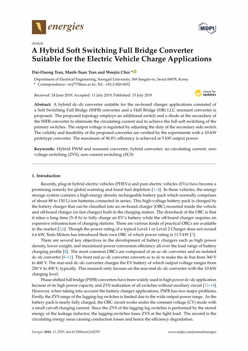
Some hybrid topologies which combine a phase-shift full bridge converter and an LLC resonantconverter have been introduced in recent studies. The main concept of hybrid topology is sharing theprimary side leg and the secondary side circuits are connected in series or parallel, as shown in Figure 1.The LLC converter operates at resonant frequency with unity voltage gain and transfers the energyto output during whole switching period while the output voltage is regulated by the phase-shiftmodulation method. By sharing the lagging leg switches, the ZVS range of lagging leg can be obtainedfrom zero to full-load condition as shown in Figure 1a–c. In Figure 1d,e, a clamping circuit includingCr, D9, and D10 is employed to reset the circulating current and to damp the voltage oscillation acrossthe secondary rectifier. Though the circulating current can be reduced as compared to the traditionphase-shift full-bridge converter, the lagging leg switches still suffer from hard switching turn-off.
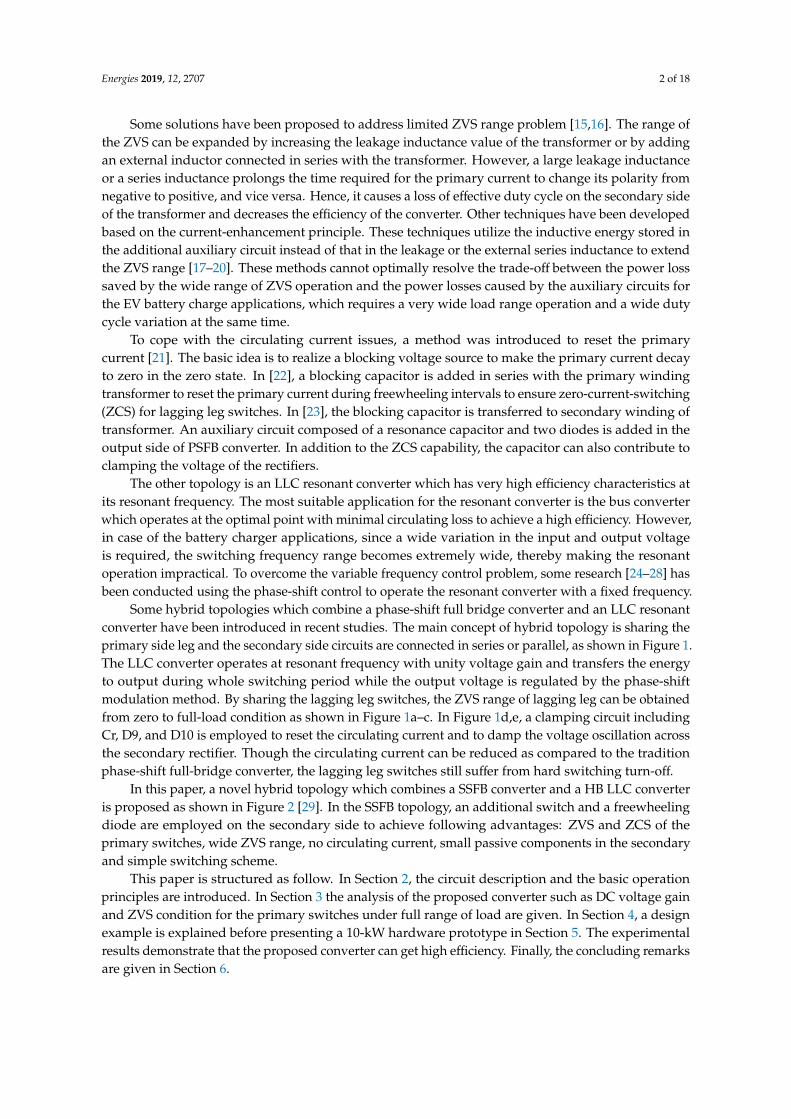
In this paper, a novel hybrid topology which combines a SSFB converter and a HB LLC converteris proposed as shown in Figure 2 [29]. In the SSFB topology, an additional switch and a freewheelingdiode are employed on the secondary side to achieve following advantages: ZVS and ZCS of theprimary switches, wide ZVS range, no circulating current, small passive components in the secondaryand simple switching scheme.
This paper is structured as follow. In Section 2, the circuit description and the basic operationprinciples are introduced. In Section 3 the analysis of the proposed converter such as DC voltage gainand ZVS condition for the primary switches under full range of load are given. In Section 4, a designexample is explained before presenting a 10-kW hardware prototype in Section 5. The experimentalresults demonstrate that the proposed converter can get high efficiency. Finally, the concluding remarksare given in Section 6.
Energies 2019, 12, 2707 3 of 18
1
1
5
Figure 1. Different types of hybrid converter. (a) Series type [24]; (b) [24] paralleled type; (c) FBconverter integrated with a symmetric half-bridge converter connected in parallel [25]; (d) hybridPWM and resonant converter with shared lagging-leg switches [26]; (e) hybrid PWM and resonantconverter with dual outputs connected in series [27]; (f) half-bridge LLC SRC integrated into a PSFBconverter [28].Energies 2019, 12, x FOR PEER REVIEW 4 of 19
96 Figure 2. Proposed hybrid dc–dc converter for the on-board charger. 97
This paper is structured as follow. In Section 2, the circuit description and the basic operation 98 principles are introduced. In Section 3 the analysis of the proposed converter such as DC voltage gain 99 and ZVS condition for the primary switches under full range of load are given. In Section 4, a design 100 example is explained before presenting a 10-kW hardware prototype in Section 5. The experimental 101 results demonstrate that the proposed converter can get high efficiency. Finally, the concluding 102 remarks are given in Section 6. 103
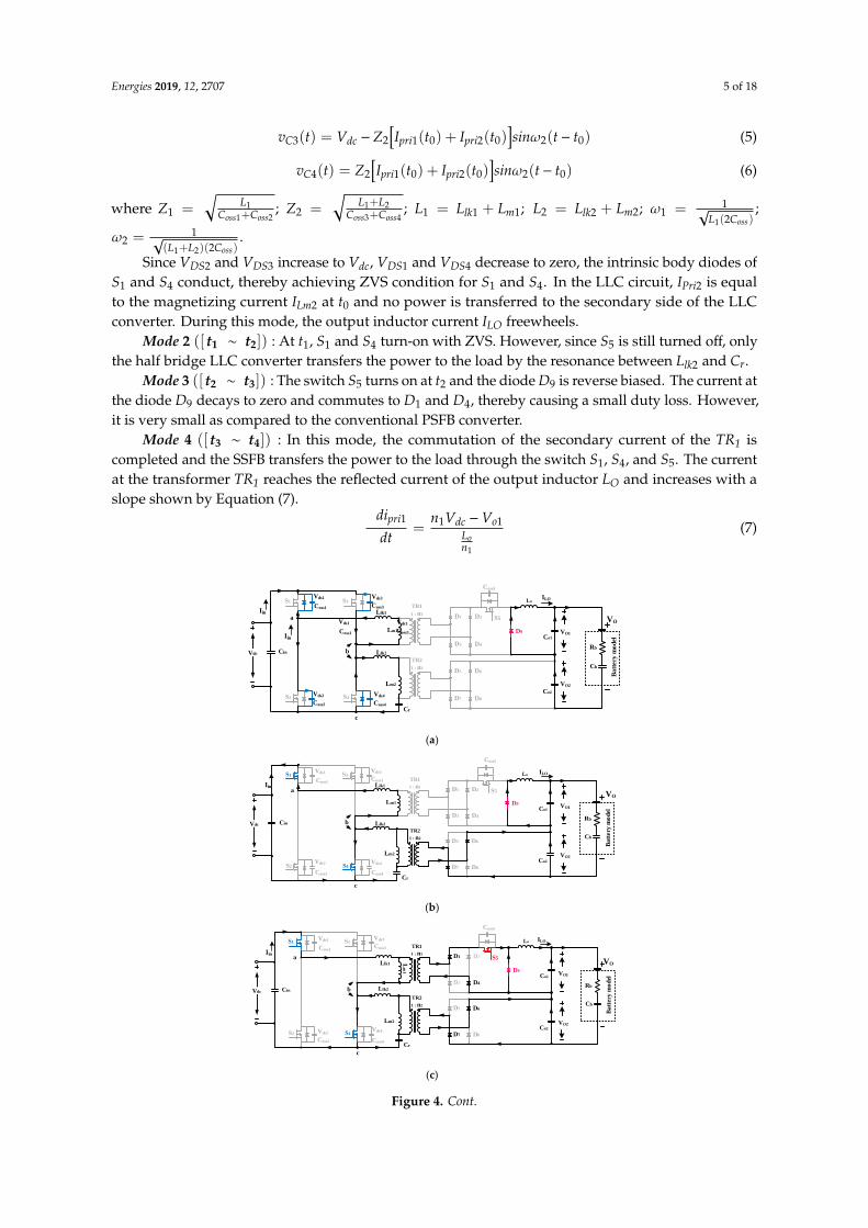
2. Operation Mode of the Proposed Hybrid Converter 104 Figure 3 shows the key waveforms of the proposed converter. In the proposed hybrid converter, 105
diagonally opposite switch pair, (𝑆 and 𝑆 ) and (𝑆 and S ), is switched at each time and the 106 secondary side switch 𝑆 is synchronized with the primary switch operation. The primary side 107 switch pair of the proposed circuit operates with a constant duty cycle of 50% at the resonant 108 frequency 𝑓 of the half bridge LLC converter while the secondary switch 𝑆 operates at 2𝑓 and its 109 duty cycle is controlled to regulate the output voltage. During the time when the secondary switch is 110 turned off, the primary current is reset, thereby achieving ZVZCS operation for the primary switches. 111
There are six operation modes of the proposed converter in a half switching period as shown in 112 Figure 4. The following assumptions are made for the simplicity of the analysis. 113 • All of the switching devices are ideal except the output capacitance. 114 • All of the capacitors, inductors, and transformer are ideal except the leakage inductance of the 115
transformer. 116 • The output capacitance values of all of the primary switches are the same. 117 • The leakage inductance values of the transformers are much smaller than the output filter 118
inductances reflected to the primary side. 𝐿 << n2 𝐿 (where n is the secondary-to-primary-119 windings-turns ratio). 120
Vo1
Vo2
S1 S3
S2 S4
TR11 : n1
TR21 : n2
Llk1
Lo
Co1
Co2
S5
CinVdc
Iin
Ipri1
Llk2
Ipri2
Lm2
ILm2
b
a
cCr
D1 D2
D3 D4
D5 D6
D7 D8
Rb
Cb
Bat
tery
mod
el
D9
Vds1
Coss1
Vds3
Coss3
Vds2
Coss2
Vds4
Coss4
Ids4Ids2
Isec1
Isec2
ID9
ILo
Lm
1ILm1
Figure 2. Proposed hybrid dc–dc converter for the on-board charger.

Energies 2019, 12, 2707 4 of 18
2. Operation Mode of the Proposed Hybrid Converter
Figure 3 shows the key waveforms of the proposed converter. In the proposed hybrid converter,diagonally opposite switch pair, (S1 and S4) and (S2 and S3), is switched at each time and the secondaryside switch S5 is synchronized with the primary switch operation. The primary side switch pair of theproposed circuit operates with a constant duty cycle of 50% at the resonant frequency fo of the halfbridge LLC converter while the secondary switch S5 operates at 2 fo and its duty cycle is controlled toregulate the output voltage. During the time when the secondary switch is turned off, the primarycurrent is reset, thereby achieving ZVZCS operation for the primary switches.
There are six operation modes of the proposed converter in a half switching period as shown inFigure 4. The following assumptions are made for the simplicity of the analysis.
• All of the switching devices are ideal except the output capacitance.• All of the capacitors, inductors, and transformer are ideal except the leakage inductance of
the transformer.• The output capacitance values of all of the primary switches are the same.• The leakage inductance values of the transformers are much smaller than the output
filter inductances reflected to the primary side. Llk<< n2 LO (where n is thesecondary-to-primary-windings-turns ratio).
Energies 2019, 12, x FOR PEER REVIEW 5 of 19
121 Figure 3. Key waveforms of the proposed converter. 122
Coss1
Vds1
VO1
IinCoss3
Vds3
Coss4
Vds4
Coss2
Vds2
VO
VO2
ILO
Coss1
Vds1
IinCoss3
Vds3
Coss5
(a)
Coss1
Vds1
IinCoss3
Vds3
Coss4
Vds4
Coss2
Vds2
VO1
VO
VO2
ILO
Coss5
(b)
Coss1
Vds1
IinCoss3
Vds3
Vds4
Coss2
Vds2
VO1
VO
VO2
ILO
Coss5
Coss4
(c)
Figure 3. Key waveforms of the proposed converter.
Mode 1 ([ t0 ∼ t1]) : At t0, one switch pair (S2 and S3) is turned off. The primary current of theSSFB transformer IPri1 charges COSS2 and COSS3, and discharges COSS1. At the same time, COSS4 isdischarged by IPri2. The primary current of two transformers and the voltages across the four switchesare given by:
ipri1(t) = Ipri1(t0)cosω1(t− t0) (1)
ipri2(t) = Ipri2(t0)cosω2(t− t0) (2)
vC1(t) = Z1Ipri1(t0)sinω1(t− t0) (3)
vC2(t) = Vdc −Z1Ipri1(t0)sinω1(t− t0) (4)
Energies 2019, 12, 2707 5 of 18
vC3(t) = Vdc −Z2[Ipri1(t0) + Ipri2(t0)
]sinω2(t− t0) (5)
vC4(t) = Z2[Ipri1(t0) + Ipri2(t0)
]sinω2(t− t0) (6)
where Z1 =√
L1Coss1+Coss2
; Z2 =√
L1+L2Coss3+Coss4
; L1 = Llk1 + Lm1; L2 = Llk2 + Lm2; ω1 = 1√L1(2Coss)
;
ω2 = 1√(L1+L2)(2Coss)
.
Since VDS2 and VDS3 increase to Vdc, VDS1 and VDS4 decrease to zero, the intrinsic body diodes ofS1 and S4 conduct, thereby achieving ZVS condition for S1 and S4. In the LLC circuit, IPri2 is equalto the magnetizing current ILm2 at t0 and no power is transferred to the secondary side of the LLCconverter. During this mode, the output inductor current ILO freewheels.
Mode 2 ([ t1 ∼ t2]) : At t1, S1 and S4 turn-on with ZVS. However, since S5 is still turned off, onlythe half bridge LLC converter transfers the power to the load by the resonance between Llk2 and Cr.
Mode 3 ([ t2 ∼ t3]) : The switch S5 turns on at t2 and the diode D9 is reverse biased. The current atthe diode D9 decays to zero and commutes to D1 and D4, thereby causing a small duty loss. However,it is very small as compared to the conventional PSFB converter.
Mode 4 ([ t3 ∼ t4]) : In this mode, the commutation of the secondary current of the TR1 iscompleted and the SSFB transfers the power to the load through the switch S1, S4, and S5. The currentat the transformer TR1 reaches the reflected current of the output inductor LO and increases with aslope shown by Equation (7).
dipri1
dt=
n1Vdc −Vo1Lon1
(7)
Energies 2019, 12, x FOR PEER REVIEW 5 of 19
Figure 3. Key waveforms of the proposed converter.
S1 S3
S2 S4
TR11 : n1
TR21 : n2
Llk1
Lo
Co1
Co2
S5
CinVdc Llk2
Lm2
b
a
cCr
D1 D2
D3 D4
D5 D6
D7 D8
Rb
Cb
Batte
ry m
odel
D9Lm1
Coss1
Vds1
VO1
IinCoss3
Vds3
Coss4
Vds4
Coss2
Vds2
VO
VO2
ILO
Coss1
Vds1
IinCoss3
Vds3
Coss5
(a)
S1 S3
S2 S4
TR11 : n1
TR21 : n2
Llk1
Lo
Co1
Co2
S5
CinVdc Llk2
Lm2
b
a
cCr
D1 D2
D3 D4
D5 D6
D7 D8
Rb
Cb
Batte
ry m
odel
D9Lm1
Coss1
Vds1
IinCoss3
Vds3
Coss4
Vds4
Coss2
Vds2
VO1
VO
VO2
ILO
Coss5
(b)
S1 S3
S2 S4
TR11 : n1
TR21 : n2
Llk1
Lo
Co1
Co2
S5
CinVdc Llk2
Lm2
b
a
cCr
D1 D2
D3 D4
D5 D6
D7 D8
Rb
Cb
Batte
ry m
odel
D9
Lm
1
Coss1
Vds1
IinCoss3
Vds3
Vds4
Coss2
Vds2
VO1
VO
VO2
ILO
Coss5
Coss4
(c)
t0 t1 t2 t4 t5 t6t3
T
S1 & S4 S2 & S3
S5
IPri1
IPri2
VDS2 VDS4
IS5 ID9
IDS1S1, S4
ZVS turn-onS1, S4
ZCS turn-off
IDS4
IDS2
Figure 4. Cont.
Energies 2019, 12, 2707 6 of 18
Energies 2019, 12, x FOR PEER REVIEW 6 of 19
S1 S3
S2 S4
TR11 : n1
TR21 : n2
Llk1
Lo
Co1
Co2
S5
CinVdc Llk2
Lm2
b
a
cCr
D1 D2
D3 D4
D5 D6
D7 D8
Rb
Cb
Batte
ry m
odel
D9
Lm
1
Coss1
Vds1
IinCoss3
Vds3
Coss4
Vds4
Coss2
Vds2
VO1
VO
VO2
ILO
Coss5
(d)
S1 S3
S2 S4
TR11 : n1
TR21 : n2
Llk1
Lo
Co1
Co2
S5
CinVdc Llk2
Lm2
b
a
cCr
D1 D2
D3 D4
D5 D6
D7 D8
Rb
Cb
Batte
ry m
odel
D9
Lm
1
Coss1
Vds1
IinCoss3
Vds3
Coss4
Vds4
Coss2
Vds2
VO1
VO
VO2
ILO
Coss5
(e)
S1 S3
S2 S4
TR11 : n1
TR21 : n2
Llk1
Lo
Co1
Co2
S5
CinVdc Llk2
Lm2
b
a
cCr
D1 D2
D3 D4
D5 D6
D7 D8
Rb
Cb
Batte
ry m
odel
D9Lm1
Coss1
Vds1
IinCoss3
Vds3
Coss4
Vds4
Coss2
Vds2
VO1
VO
VO2
ILO
Coss5
(f)
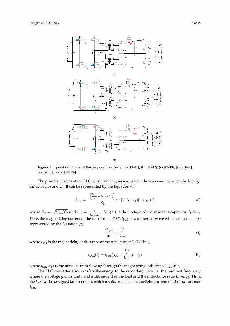
Figure 4. Operation modes of the proposed converter (a) [t0~t1], (b) [t1~t2], (c) [t2~t3], (d) [t3~t4], (e) 123 [t4~t5], and (f) [t5~t6]. 124 𝑴𝒐𝒅𝒆 𝟏 ([𝒕𝟎 ~ 𝒕𝟏]): At 𝑡 , one switch pair (𝑆 and 𝑆 ) is turned off. The primary current of the 125
SSFB transformer 𝐼 charges 𝐶 and 𝐶 , and discharges 𝐶 . At the same time, 𝐶 is 126 discharged by 𝐼 . The primary current of two transformers and the voltages across the four 127 switches are given by: 128 𝑖 (𝑡) = 𝐼 (𝑡 )𝑐𝑜𝑠𝜔 (𝑡 − 𝑡 ) (1) 𝑖 (𝑡) = 𝐼 (𝑡 )𝑐𝑜𝑠𝜔 (𝑡 − 𝑡 ) (2) 𝑣 (𝑡) = 𝑍 𝐼 (𝑡 )𝑠𝑖𝑛𝜔 (𝑡 − 𝑡 ) (3) 𝑣 (𝑡) = 𝑉 − 𝑍 𝐼 (𝑡 )𝑠𝑖𝑛𝜔 (𝑡 − 𝑡 ) (4) 𝑣 (𝑡) = 𝑉 − 𝑍 𝐼 (𝑡 ) + 𝐼 (𝑡 ) 𝑠𝑖𝑛𝜔 (𝑡 − 𝑡 ) (5) 𝑣 (𝑡) = 𝑍 𝐼 (𝑡 ) + 𝐼 (𝑡 ) 𝑠𝑖𝑛𝜔 (𝑡 − 𝑡 ) (6)
where 𝑍 = ; 𝑍 = ; 𝐿 = 𝐿 + 𝐿 ; 𝐿 = 𝐿 + 𝐿 ; 𝜔 = ( ) ; 𝜔2 =129 1(𝐿1+𝐿2)(2𝐶𝑜𝑠𝑠). 130 Since 𝑉 and 𝑉 increase to 𝑉 , 𝑉 and 𝑉 decrease to zero, the intrinsic body diodes 131
of 𝑆 and 𝑆 conduct, thereby achieving ZVS condition for 𝑆 and 𝑆 . In the LLC circuit, 𝐼 is 132
Figure 4. Operation modes of the proposed converter (a) [t0~t1], (b) [t1~t2], (c) [t2~t3], (d) [t3~t4],(e) [t4~t5], and (f) [t5~t6].
The primary current of the LLC converter, IPri2, increases with the resonance between the leakageinductor Llk2 and Cr. It can be represented by the Equation (8).
ipri2 = −
[Vin2 −VCr(t3)
]Z0
sin[ω0(t− t4)] − iLm2(t) (8)
where Z0 =√
Llk2/Cr and ω0 = 1√Llk2Cr
. VCr(t3) is the voltage of the resonant capacitor Cr at t3.
Here, the magnetizing current of the transformer TR2, ILm2, is a triangular wave with a constant sloperepresented by the Equation (9).
diLm2
dt=
Vin2
Lm2(9)
where Lm2 is the magnetizing inductance of the transformer TR2. Thus,
iLm2(t) = iLm2( t3) +
Vin2
Lm2(t− t3) (10)
where iLm2(t3) is the initial current flowing through the magnetizing inductance Lm2 at t3.The LLC converter also transfers the energy to the secondary circuit at the resonant frequency
where the voltage gain is unity and independent of the load and the inductance ratio Lm2/Llk2. Thus,the Lm2 can be designed large enough, which results in a small magnetizing current of LLC transformer,ILm2.
Energies 2019, 12, 2707 7 of 18
Mode 5 ([ t4 ∼ t5]) : At t4 , S5 is turned off and the voltage across S5 is increased. The diode D9
is forward biased and the current commutation starts to occur from D1 and D4 to D9. The currentIPri1 resets to almost zero current during this mode. Hence, the circulating current can be eliminated,and hence the loss associated with it. The LLC converter operation remains the same as that in theprevious mode.
Mode 6 ([ t5 ∼ t6]) : At t6, S1, and S4 are turned off under ZCS condition. The outputinductor current ILO freewheels through D9. The LLC converter operations remains the sameas the previous mode.
Since the operation principle of the other half of a switching period is same as the above, it isomitted here.
3. Design Considerations for the Proposed Hybrid Converter
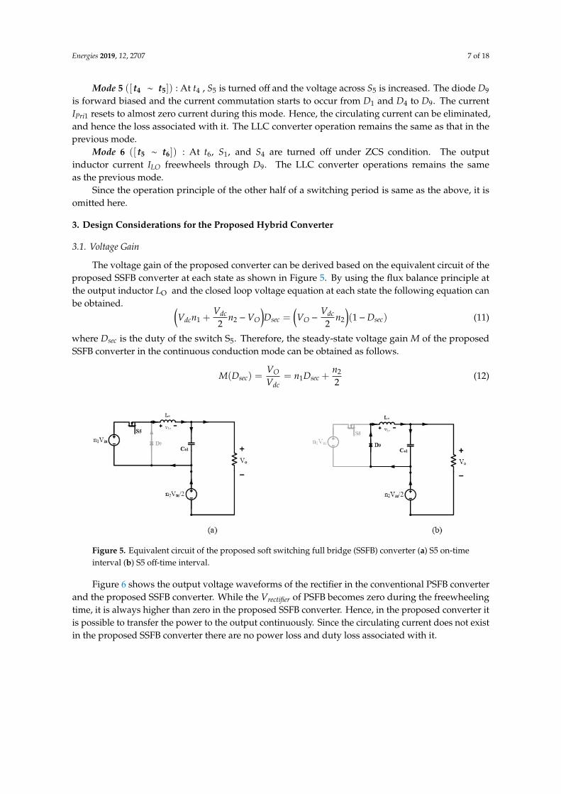
3.1. Voltage Gain
The voltage gain of the proposed converter can be derived based on the equivalent circuit of theproposed SSFB converter at each state as shown in Figure 5. By using the flux balance principle atthe output inductor LO and the closed loop voltage equation at each state the following equation canbe obtained. (
Vdcn1 +Vdc2
n2 −VO
)Dsec =
(VO −
Vdc2
n2
)(1−Dsec) (11)
where Dsec is the duty of the switch S5. Therefore, the steady-state voltage gain M of the proposedSSFB converter in the continuous conduction mode can be obtained as follows.
M(Dsec) =VOVdc
= n1Dsec +n2
2(12)
1
1
5 Figure 5. Equivalent circuit of the proposed soft switching full bridge (SSFB) converter (a) S5 on-timeinterval (b) S5 off-time interval.
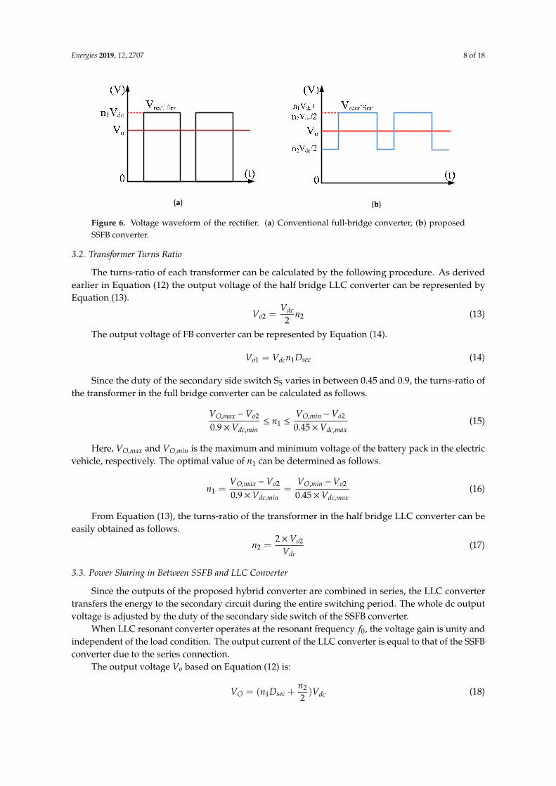
Figure 6 shows the output voltage waveforms of the rectifier in the conventional PSFB converterand the proposed SSFB converter. While the Vrectifier of PSFB becomes zero during the freewheelingtime, it is always higher than zero in the proposed SSFB converter. Hence, in the proposed converter itis possible to transfer the power to the output continuously. Since the circulating current does not existin the proposed SSFB converter there are no power loss and duty loss associated with it.
Energies 2019, 12, 2707 8 of 18
Energies 2019, 12, x FOR PEER REVIEW 8 of 19
The voltage gain of the proposed converter can be derived based on the equivalent circuit of the 168 proposed SSFB converter at each state as shown in Figure 5. By using the flux balance principle at the 169 output inductor 𝐿 and the closed loop voltage equation at each state the following equation can be 170 obtained. 171
𝑉 𝑛 + 𝑉2 𝑛 − 𝑉 𝐷 = 𝑉 − 𝑉2 𝑛 (1 − 𝐷 ) (11)
where 𝐷 is the duty of the switch S5. Therefore, the steady-state voltage gain M of the proposed 172 SSFB converter in the continuous conduction mode can be obtained as follows. 173 𝑀(𝐷 ) = 𝑉𝑉 = 𝑛 𝐷 + 𝑛2 (12)
174 Figure 5. Equivalent circuit of the proposed soft switching full bridge (SSFB) converter (a) S5 on-time 175 interval (b) S5 off-time interval. 176
Figure 6 shows the output voltage waveforms of the rectifier in the conventional PSFB converter 177 and the proposed SSFB converter. While the Vrectifier of PSFB becomes zero during the freewheeling 178 time, it is always higher than zero in the proposed SSFB converter. Hence, in the proposed converter 179 it is possible to transfer the power to the output continuously. Since the circulating current does not 180 exist in the proposed SSFB converter there are no power loss and duty loss associated with it. 181
182 Figure 6. Voltage waveform of the rectifier. (a) Conventional full-bridge converter, (b) proposed SSFB 183 converter. 184
3.2. Transformer Turns Ratio 185 The turns-ratio of each transformer can be calculated by the following procedure. As derived 186
earlier in Equation (12) the output voltage of the half bridge LLC converter can be represented by 187 Equation (13). 188
(a)
(b)
(a)
(b)
Figure 6. Voltage waveform of the rectifier. (a) Conventional full-bridge converter, (b) proposedSSFB converter.
3.2. Transformer Turns Ratio
The turns-ratio of each transformer can be calculated by the following procedure. As derivedearlier in Equation (12) the output voltage of the half bridge LLC converter can be represented byEquation (13).
Vo2 =Vdc2
n2 (13)
The output voltage of FB converter can be represented by Equation (14).
Vo1 = Vdcn1Dsec (14)
Since the duty of the secondary side switch S5 varies in between 0.45 and 0.9, the turns-ratio ofthe transformer in the full bridge converter can be calculated as follows.
VO,max −Vo2
0.9×Vdc,min≤ n1 ≤
VO,min −Vo2
0.45×Vdc,max(15)
Here, VO,max and VO,min is the maximum and minimum voltage of the battery pack in the electricvehicle, respectively. The optimal value of n1 can be determined as follows.
n1 =VO,max −Vo2
0.9×Vdc,min=
VO,min −Vo2
0.45×Vdc,max(16)
From Equation (13), the turns-ratio of the transformer in the half bridge LLC converter can beeasily obtained as follows.
n2 =2×Vo2
Vdc(17)
3.3. Power Sharing in Between SSFB and LLC Converter
Since the outputs of the proposed hybrid converter are combined in series, the LLC convertertransfers the energy to the secondary circuit during the entire switching period. The whole dc outputvoltage is adjusted by the duty of the secondary side switch of the SSFB converter.
When LLC resonant converter operates at the resonant frequency f0, the voltage gain is unity andindependent of the load condition. The output current of the LLC converter is equal to that of the SSFBconverter due to the series connection.
The output voltage Vo based on Equation (12) is:
VO = (n1Dsec +n2
2)Vdc (18)

Energies 2019, 12, 2707 9 of 18
The ratio of the power assigned for SSFB and LLC converter at a certain output power Po,β1 and β2,can be derived as in Equations (19) and (20).
β1 =PSSFB
PO
n1Dsec
n1Dsec +n22
(19)
β2 =PLLCPO
n22
n1Dsec +n22
(20)
3.4. ZVS Condition of the Primary Switches
In the proposed hybrid converter, two primary currents in TR1 and TR2 are participating chargingand discharging the parasitic output capacitances of the four primary switches. Figure 7 shows theequivalent circuit formed in the mode 1.
Energies 2019, 12, x FOR PEER REVIEW 10 of 19
𝑖 (𝑡) + 𝑖 (𝑡) = 𝐶 𝑑𝑣𝑑𝑡 + 𝐶 𝑑𝑣𝑑𝑡 (22)
Since Cr >> (Coss3 + Coss4) and Llk + Lm >> Llk, 𝑖 (𝑡) and 𝑖 (𝑡) can be treated as a constant 213 current source, respectively. 214
The peak value of the magnetizing current of TR1 can be represented as follows. 215
𝐼 , = 𝑉4𝐿 𝑓 (23)
The peak value of the magnetizing current of TR2 can be represented as follows. 216
𝐼 , = 𝑉 /24𝐿 𝑓 (24)
In the proposed hybrid SSFB converter the ZVS condition for the primary switches can be 217 achieved all over the load range because the peak values of 𝐼 and 𝐼 are independent of the 218 load as shown in Equation (23) and (24). For the simplicity of the design 𝐼 , and 𝐼 , need 219 to be designed sufficient to charge three parasitic output capacitors of the primary switches and to 220 discharge one parasitic output capacitor of the primary switch, respectively. Taking it into 221 consideration that 𝑡 is typically less than 5% of a switching period, the magnetizing inductances 222 𝐿 and 𝐿 should be designed to satisfy the following condition to guarantee ZVS of the primary 223 switches all over the load condition as follows. 224 𝐿 ≤ 𝑡 /[4(3 × 𝐶 )𝑓 ] (25) 𝐿 ≤ 𝑡 /[16(𝐶 )𝑓 ] (26)
225 Figure 7. Equivalent circuit of the proposed hybrid converter during mode 1. 226
3.5. ZCS Condition for the Primary Switches 227 In the proposed hybrid converter the primary switch pair turns off after the secondary switch 228 𝑆 turns off. If the primary switch turns off after the secondary switch turns off, the ZCS turn-off 229
condition for the primary switches can be achieved. Hence, the 𝐼 can be reset to zero before the 230 primary switches turn off as shown in Figure 8. The minimum interval 𝑡 to achieve the ZCS 231 condition can be represented by Equation (27). 232 𝑡 > 𝑛 𝐿𝑉 𝐼 (27)
where 𝐼 is the reflected output current 𝐼 to the primary side of SSFB converter. 233
Ipri1
Coss1 Coss3
Coss4Coss2
VdcIpri2
Figure 7. Equivalent circuit of the proposed hybrid converter during mode 1.
In the mode 1 [t0 − t1], Coss2 is charged and Coss1 is discharged by ipri1 as shown in Equation (21).
ipri1(t) = Coss1dvDS1
dt+ Coss2
dvDS2
dt(21)
COSS3 is charged and COSS4 is discharged by the sum of ipri1 and ipri2 as shown in Equation (22).
ipri1(t) + ipri2(t) = Coss3dvDS3
dt+ Coss4
dvDS4
dt(22)
Since Cr >> (Coss3 + Coss4) and Llk + Lm >> Llk, ipri1(t) and ipri2(t) can be treated as a constantcurrent source, respectively.
The peak value of the magnetizing current of TR1 can be represented as follows.
ILm1,peak =Vdc
4Lm1 fo(23)
The peak value of the magnetizing current of TR2 can be represented as follows.
ILm2,peak =Vdc/24Lm2 fo
(24)
In the proposed hybrid SSFB converter the ZVS condition for the primary switches can be achievedall over the load range because the peak values of ILm1 and ILm2 are independent of the load as shownin Equations (23) and (24). For the simplicity of the design ILm1,peak and ILm2,peak need to be designedsufficient to charge three parasitic output capacitors of the primary switches and to discharge oneparasitic output capacitor of the primary switch, respectively. Taking it into consideration that tdeadis typically less than 5% of a switching period, the magnetizing inductances Lm1 and Lm2 should be
Energies 2019, 12, 2707 10 of 18
designed to satisfy the following condition to guarantee ZVS of the primary switches all over the loadcondition as follows.
Lm1 ≤ tdead/[4(3×Coss) f0] (25)
Lm2 ≤ tdead/[16(Coss) f0] (26)
3.5. ZCS Condition for the Primary Switches
In the proposed hybrid converter the primary switch pair turns off after the secondary switch S5
turns off. If the primary switch turns off after the secondary switch turns off, the ZCS turn-off conditionfor the primary switches can be achieved. Hence, the IPri1 can be reset to zero before the primaryswitches turn off as shown in Figure 8. The minimum interval tZCS to achieve the ZCS condition can berepresented by Equation (27).
tZCS >n1Llk1
VdcIo1 (27)
where IO1 is the reflected output current IO to the primary side of SSFB converter.Energies 2019, 12, x FOR PEER REVIEW 11 of 19
234 Figure 8. Minimum interval to achieve zero current switching (ZCS) condition for the primary 235 switches. 236
3.6. Design of the Output Inductor 237 The inductor at the output filter can be derived from the rectifier output voltage in Figure 6b. 238 𝑉 = 𝐿 ∆𝐼∆𝑇 (28)
where ∆𝐼 is the peak-to-peak value of the current at 𝐿 and 𝑉 is the voltage applied to LO during 239 ∆T = 𝐷 𝑇 /2. 240 For the proposed converter 241
𝐿 _ = (𝑉 − 𝑛 𝑉2 )(1 − 𝐷)𝑇2∆𝐼 (29)
For the conventional PSFB converter 242
𝐿 _ = 𝑉 𝑇2∆𝐼 × (1 − D) (30)
In case of EV chargers, the current ripple at LO is worst when the voltage of the battery is lowest, 243 VO = 330 V. 244
4. Design of the Proposed SSFB Converter for Electric Vehicle Charge Application 245 In this section the design procedure for the proposed converter is presented. Table I shows the 246
specification of the proposed converter for the electric vehicle charge application. 247
Table 1. Design specification of the proposed converter. 248
Parameter Designator Value Input Voltage Range 𝑉 , ~ 𝑉 , 380–400 [V]
Input Voltage Nominal 𝑉 , 390 [V] Output Voltage Range 𝑉 , ~ 𝑉 , 330–430 [V]
Output Voltage Nominal 𝑉 , 400 [V] Maximum Output Power 𝑃 , 10 [kW]
Switching frequency 𝑓 29.4 [kHz]
4.1. Turns Ratio of the Transformer 249 The optimal turns ratio of the transformer in the SSFB converter can be calculated by using 250
Equation (16). Both sides of Equation (16) have been drawn as shown in Figure 9 and the cross point 251 of two lines is the design point. Therefore, the optimal turns ratio of the transformer in the SSFB, 𝑛 , 252
Figure 8. Minimum interval to achieve zero current switching (ZCS) condition for the primary switches.
3.6. Design of the Output Inductor
The inductor at the output filter can be derived from the rectifier output voltage in Figure 6b.
VLo = Lo∆Io
∆T(28)
where ∆Io is the peak-to-peak value of the current at Lo and VLo is the voltage applied to LO during∆T = DsecTs/2.
For the proposed converter
LO_proposed =(Vo −
n2Vdc2 )(1−D)Ts
2∆Io(29)
For the conventional PSFB converter
LO_conventional =VoTs
2∆Io× (1−D) (30)
In case of EV chargers, the current ripple at LO is worst when the voltage of the battery is lowest,VO = 330 V.

Energies 2019, 12, 2707 11 of 18
4. Design of the Proposed SSFB Converter for Electric Vehicle Charge Application
In this section the design procedure for the proposed converter is presented. Table 1 shows thespecification of the proposed converter for the electric vehicle charge application.
Table 1. Design specification of the proposed converter.
Parameter Designator Value
Input Voltage Range Vdc,min ∼ Vdc,max 380–400 [V]Input Voltage Nominal Vdc,nom 390 [V]Output Voltage Range Vo,min ∼ Vo,max 330–430 [V]
Output Voltage Nominal Vo,nom 400 [V]Maximum Output Power Po,max 10 [kW]
Switching frequency fs 29.4 [kHz]
4.1. Turns Ratio of the Transformer
The optimal turns ratio of the transformer in the SSFB converter can be calculated by usingEquation (16). Both sides of Equation (16) have been drawn as shown in Figure 9 and the cross pointof two lines is the design point. Therefore, the optimal turns ratio of the transformer in the SSFB, n1,is selected as 0.6 and the output voltage of the LLC converter is 220 V. The turns ratio of the transformerin the HB LLC, n2, can be easily calculated as 1.12 by using Equation (17).
Energies 2019, 12, x FOR PEER REVIEW 12 of 19
is selected as 0.6 and the output voltage of the LLC converter is 220 V. The turns ratio of the 253 transformer in the HB LLC, 𝑛 , can be easily calculated as 1.12 by using Equation (17). 254
255 Figure 9. Optimal design point of SSFB transformer turn ratio. 256
At nominal output voltage 𝑉 = 400V, the power of the LLC converter and SSFB converter are 257 calculated simply as follows. 𝑃 = 220V/400V × 10 𝑘𝑊 = 5.5 𝑘𝑊, hence 𝑃 = 4.5 𝑘𝑊. 258
4.2. SSFB Transformer TR1 259 The magnetizing inductance 𝐿 can be calculated from Equation (25). Given 𝐶 = 𝐶 =260 1000 𝑝𝐹, 𝑓 = 29.4 𝑘𝐻𝑧 𝑎𝑛𝑑 𝑡 = 2% ∗ 𝑇 , 𝐿 ≤ 1.9 𝑚𝐻. 261 The core selection for the SSFB transformer can be performed as follows [12] 262
𝑃 = 0.0005 × 𝐵 × 𝑓 × 𝐴 𝐴𝐷 (31)
𝐴 , = 𝐴 𝐴 = 𝑃 𝐷0.0005 × 𝐵 × 𝑓 (32)
where 𝐴 , is area product of SSFB transformer core (cm4), 𝐴 is core area (cm2), 𝐴 is bobbin 263 winding area (cm2), current density 𝐷 = 400 cir.mils/amp, flux density 𝐵 = 2000 gauss and 264 𝑃 = 4.5kW. By using Equation (31), we can calculate 𝐴 , = 61.2 cm4. 265
As mentioned earlier in section 3.4, zero voltage switching is independent of the value of 𝐿 . 266 Thus, 𝐿 can be designed as small as possible to reduce duty cycle loss and resetting time of the 267 primary current. 268
The magnetizing inductor has been designed by selecting a gapless high permeability core 269 material. A PQ72/52 is selected and 𝐴 = 64 cm4. 270
4.3. LLC Transformer TR2 271 While the parallel type hybrid converter in [25] where TR2 is typically considered as an auxiliary 272
transformer to assist the ZVS of lagging leg switches, the series type hybrid converter requires a large 273 TR2 to handle the current at the lowest output voltage condition. The calculation of LLC transformer 274 can be performed similar to SSFB transformer. However, TR1 and TR2 can be designed with a same 275 size core to enhance the power density [27]. Therefore, the same core PQ72/52 is selected for the 276 transformer TR2. 277
The magnetizing inductance 𝐿 must meet the Equation (26) to guarantee ZVS at no-load 278 condition. Given 𝐶 = 𝐶 = 1000 𝑝𝐹, 𝐿 ≤ 1.4 𝑚𝐻. 279
Design of the resonant parameters Llk2 and Cr can be performed based on the ZVS constraint at 280 full-load condition. The reasonable value of the quality factor 𝑄 is selected as 1.3 [28] 281 𝐿 = 𝑄 𝑅 , /(2𝜋𝑓 ) (33)
The equivalent ac resistance at full load can 282
Figure 9. Optimal design point of SSFB transformer turn ratio.
At nominal output voltage VO = 400 V, the power of the LLC converter and SSFB converter arecalculated simply as follows. PLLC = 220V/400V× 10 kW = 5.5 kW, hence PSSFB = 4.5 kW.
4.2. SSFB Transformer TR1
The magnetizing inductance Lm1 can be calculated from Equation (25). Given Coss1 = Coss2 =
1000 pF, f0 = 29.4 kHz and tdead = 2%∗T0, Lm1 ≤ 1.9 mH. The core selection for the SSFB transformercan be performed as follows [12]
PSSFB =0.0005× Bmax × fs ×AeAb
Dcma(31)
AP,SSFB = AeAb =PSSFBDcma
0.0005× Bmax × fs(32)
where AP,SSFB is area product of SSFB transformer core (cm4), Ae is core area (cm2), Ab is bobbinwinding area (cm2), current density Dcma = 400 cir.mils/amp, flux density Bmax = 2000 gauss andPSSFB = 4.5 kW. By using Equation (31), we can calculate AP,SSFB = 61.2 cm4.
Energies 2019, 12, 2707 12 of 18
As mentioned earlier in Section 3.4, zero voltage switching is independent of the value of Llk1.Thus, Llk1 can be designed as small as possible to reduce duty cycle loss and resetting time of theprimary current.
The magnetizing inductor has been designed by selecting a gapless high permeability core material.A PQ72/52 is selected and AP = 64 cm4.
4.3. LLC Transformer TR2
While the parallel type hybrid converter in [25] where TR2 is typically considered as an auxiliarytransformer to assist the ZVS of lagging leg switches, the series type hybrid converter requires a largeTR2 to handle the current at the lowest output voltage condition. The calculation of LLC transformercan be performed similar to SSFB transformer. However, TR1 and TR2 can be designed with a samesize core to enhance the power density [27]. Therefore, the same core PQ72/52 is selected for thetransformer TR2.
The magnetizing inductance Lm2 must meet the Equation (26) to guarantee ZVS at no-loadcondition. Given Coss1 = Coss2 = 1000 pF, Lm2 ≤ 1.4 mH. Design of the resonant parameters Llk2 andCr can be performed based on the ZVS constraint at full-load condition. The reasonable value of thequality factor QZVS is selected as 1.3 [28]
Llk2 = QZVSRac,min/(2π fr) (33)
The equivalent ac resistance at full load can
Rac,min =8 n2
2
π2 Ro,min (34)
At the full load condition of LLC converter Ro,min = 8.8 Ω. Therefore, Llk2 = 60.7 µH.
4.4. Resonant Capacitance
Since LLC circuit operates at the resonant frequency f0, the resonant capacitor Cr can be calculatedby using Equation (35).
Cr =1
Llk2(2π f0)2 (35)
Therefore, Cr = 0.482 µF
4.5. Output Inductor
From the earlier analysis in Section 3.6, the output inductor value can be obtained by
LO_proposed =(Vo_min −
n2Vdc2 )(1−Dmin)Ts
2∆Io(36)
When Vo_min = 330 V, Dmin = 0.45 and ∆Io = 5%∗Io_max = 5%∗(Po/Vo_min), LO_proposed is calculatedas 679 µH.
The key parameters of the design and the actual parameters obtained in implementation are givenin Table 2. The circuit components used in the prototype converter are given in Table 3.
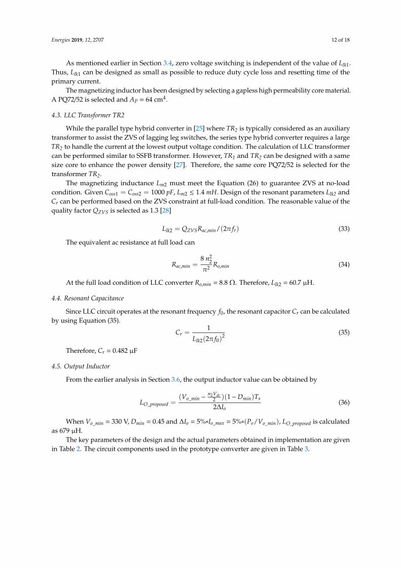
Energies 2019, 12, 2707 13 of 18
Table 2. Key parameters of the design and implementation.
Parameter Calculated Value Measured Value
Turn ratio of the TR1 (n11 : n12) 11 : 7 11 : 7Leakage inductance of the TR1 (Llk1) 12.4 [µH]
Magnetizing inductance of the TR1 (Lm1) Lm1 < 1.9 [mH] 1.5 [mH]Turn ratio of the TR2 (n21 : n22) 14 : 16 14 : 16
Leakage inductance of the TR2 (Llk2) 60.7 [µH] 65 [µH]Magnetizing inductance of the TR2 (Lm2) Lm2 < 1.4 [mH] 800 [µH]
Resonant capacitor (Cr) 0.482 [µF] 0.45 [µF]Output inductor of SSFB converter (LO) 679 [µH] 685 [µH]
Table 3. Components used in the prototype converter.
Component Manufacture Part#
Primary side MOSFETs Fairchild FCH76N60NSecondary side MOSFETs IXYZ IXFB110N60P3
Diode Rectifiers IR 60APU06Resonant Film Capacitors EPCOS B32912B3334M
Magnetic Ferrite Core of Transformer Changsung PQ7252
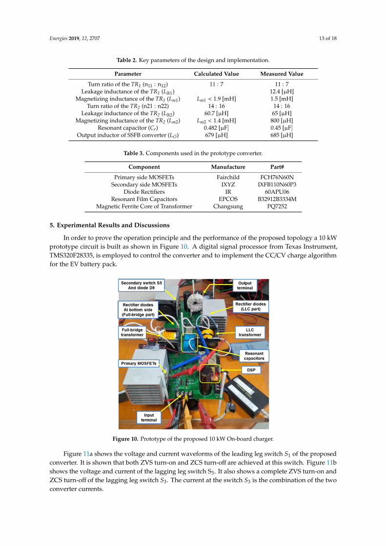
5. Experimental Results and Discussions
In order to prove the operation principle and the performance of the proposed topology a 10 kWprototype circuit is built as shown in Figure 10. A digital signal processor from Texas Instrument,TMS320F28335, is employed to control the converter and to implement the CC/CV charge algorithmfor the EV battery pack.Energies 2019, 12, x FOR PEER REVIEW 14 of 19
301 Figure 10. Prototype of the proposed 10 kW On-board charger. 302
Figure 11a shows the voltage and current waveforms of the leading leg switch 𝑆 of the 303 proposed converter. It is shown that both ZVS turn-on and ZCS turn-off are achieved at this switch. 304 Figure 11b shows the voltage and current of the lagging leg switch S . It also shows a complete ZVS 305 turn-on and ZCS turn-off of the lagging leg switch 𝑆 . The current at the switch 𝑆 is the combination 306 of the two converter currents. 307
Figure 10. Prototype of the proposed 10 kW On-board charger.
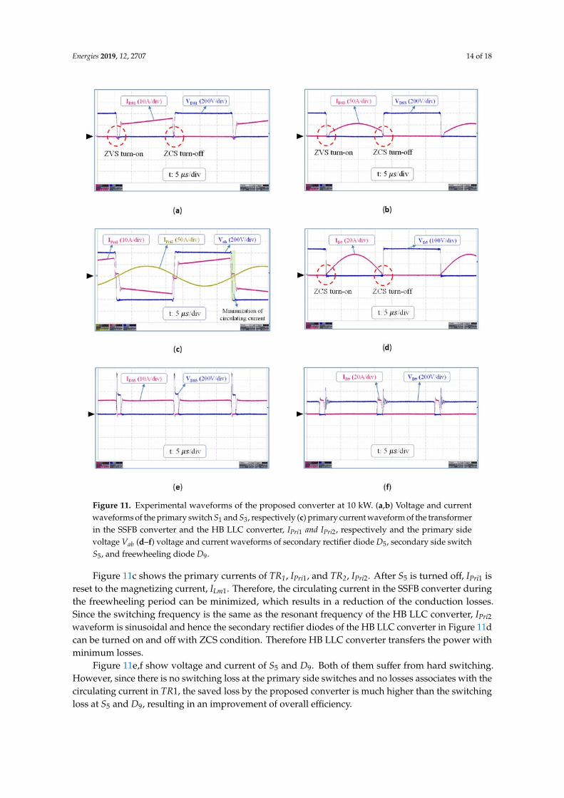
Figure 11a shows the voltage and current waveforms of the leading leg switch S1 of the proposedconverter. It is shown that both ZVS turn-on and ZCS turn-off are achieved at this switch. Figure 11bshows the voltage and current of the lagging leg switch S3. It also shows a complete ZVS turn-on andZCS turn-off of the lagging leg switch S3. The current at the switch S3 is the combination of the twoconverter currents.
Energies 2019, 12, 2707 14 of 18
2
11
Figure 11. Experimental waveforms of the proposed converter at 10 kW. (a,b) Voltage and currentwaveforms of the primary switch S1 and S3, respectively (c) primary current waveform of the transformerin the SSFB converter and the HB LLC converter, IPri1 and IPri2, respectively and the primary sidevoltage Vab (d–f) voltage and current waveforms of secondary rectifier diode D5, secondary side switchS5, and freewheeling diode D9.
Figure 11c shows the primary currents of TR1, IPri1, and TR2, IPri2. After S5 is turned off, IPri1 isreset to the magnetizing current, ILm1. Therefore, the circulating current in the SSFB converter duringthe freewheeling period can be minimized, which results in a reduction of the conduction losses.Since the switching frequency is the same as the resonant frequency of the HB LLC converter, IPri2waveform is sinusoidal and hence the secondary rectifier diodes of the HB LLC converter in Figure 11dcan be turned on and off with ZCS condition. Therefore HB LLC converter transfers the power withminimum losses.
Figure 11e,f show voltage and current of S5 and D9. Both of them suffer from hard switching.However, since there is no switching loss at the primary side switches and no losses associates with thecirculating current in TR1, the saved loss by the proposed converter is much higher than the switchingloss at S5 and D9, resulting in an improvement of overall efficiency.
Energies 2019, 12, 2707 15 of 18
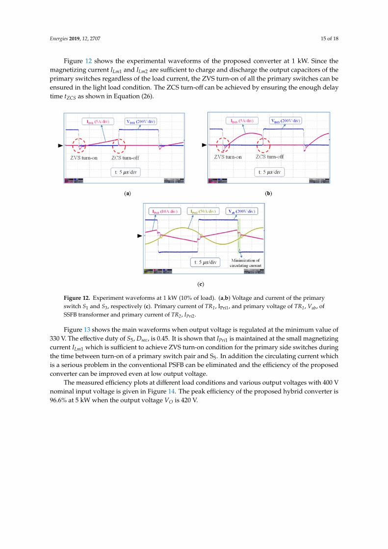
Figure 12 shows the experimental waveforms of the proposed converter at 1 kW. Since themagnetizing current ILm1 and ILm2 are sufficient to charge and discharge the output capacitors of theprimary switches regardless of the load current, the ZVS turn-on of all the primary switches can beensured in the light load condition. The ZCS turn-off can be achieved by ensuring the enough delaytime tZCS as shown in Equation (26).
3
12
13
Figure 12. Experiment waveforms at 1 kW (10% of load). (a,b) Voltage and current of the primaryswitch S1 and S3, respectively (c). Primary current of TR1, IPri1, and primary voltage of TR1, Vab, ofSSFB transformer and primary current of TR2, IPri2.
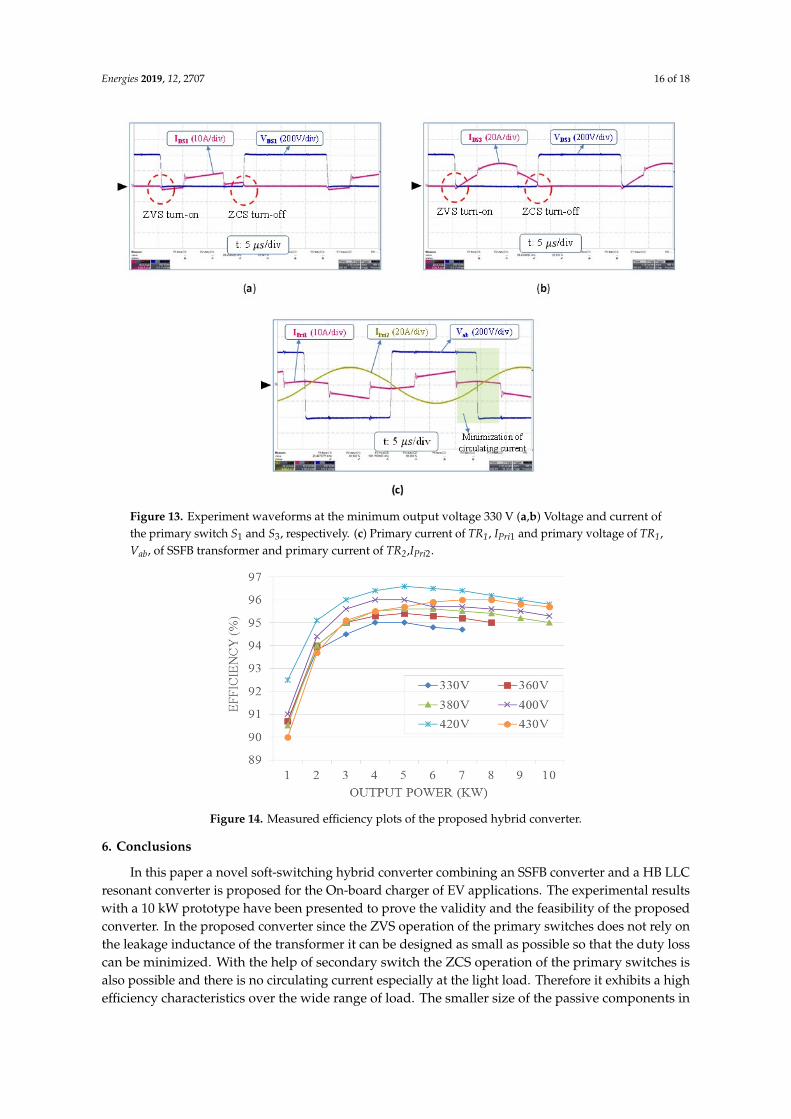
Figure 13 shows the main waveforms when output voltage is regulated at the minimum value of330 V. The effective duty of S5, Dsec, is 0.45. It is shown that IPri1 is maintained at the small magnetizingcurrent ILm1 which is sufficient to achieve ZVS turn-on condition for the primary side switches duringthe time between turn-on of a primary switch pair and S5. In addition the circulating current whichis a serious problem in the conventional PSFB can be eliminated and the efficiency of the proposedconverter can be improved even at low output voltage.
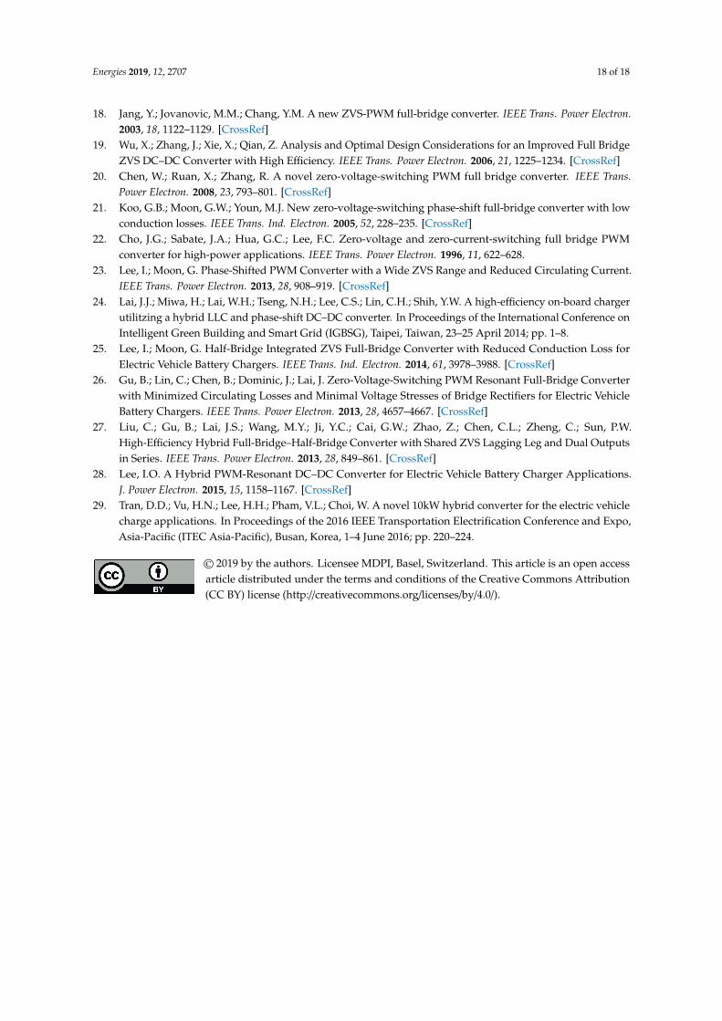
The measured efficiency plots at different load conditions and various output voltages with 400 Vnominal input voltage is given in Figure 14. The peak efficiency of the proposed hybrid converter is96.6% at 5 kW when the output voltage VO is 420 V.
Energies 2019, 12, 2707 16 of 18
3
12
13 Figure 13. Experiment waveforms at the minimum output voltage 330 V (a,b) Voltage and current ofthe primary switch S1 and S3, respectively. (c) Primary current of TR1, IPri1 and primary voltage of TR1,Vab, of SSFB transformer and primary current of TR2,IPri2.
Energies 2019, 12, x FOR PEER REVIEW 17 of 19
340 Figure 13. Experiment waveforms at the minimum output voltage 330 V (a),(b) Voltage and current 341 of the primary switch 𝑆 and 𝑆 , respectively. (c) Primary current of TR1, 𝐼 and primary voltage 342 of TR1, 𝑉 , of SSFB transformer and primary current of TR2 ,𝐼 . 343
The measured efficiency plots at different load conditions and various output voltages with 400 344 V nominal input voltage is given in Figure 14. The peak efficiency of the proposed hybrid converter 345 is 96.6% at 5 kW when the output voltage VO is 420 V. 346
347 Figure 14. Measured efficiency plots of the proposed hybrid converter. 348
6. Conclusions 349 In this paper a novel soft-switching hybrid converter combining an SSFB converter and a HB 350
LLC resonant converter is proposed for the On-board charger of EV applications. The experimental 351 results with a 10 kW prototype have been presented to prove the validity and the feasibility of the 352 proposed converter. In the proposed converter since the ZVS operation of the primary switches does 353
Figure 14. Measured efficiency plots of the proposed hybrid converter.
6. Conclusions
In this paper a novel soft-switching hybrid converter combining an SSFB converter and a HB LLCresonant converter is proposed for the On-board charger of EV applications. The experimental resultswith a 10 kW prototype have been presented to prove the validity and the feasibility of the proposedconverter. In the proposed converter since the ZVS operation of the primary switches does not rely onthe leakage inductance of the transformer it can be designed as small as possible so that the duty losscan be minimized. With the help of secondary switch the ZCS operation of the primary switches isalso possible and there is no circulating current especially at the light load. Therefore it exhibits a highefficiency characteristics over the wide range of load. The smaller size of the passive components in

Energies 2019, 12, 2707 17 of 18
the secondary side and the simple switching scheme can be considered as additional advantages of theproposed converter.
Author Contributions: Author Contributions: D.T. wrote the manuscript and designed the prototype of theproposed converter; M.T. analyzed the proposed converter; W.C. reviewed the manuscript and supervisedthe research.
Funding: This research was funded by the KEPCO (Korean Electric Power Corporation; Grant number:R17XA05-42).
Acknowledgments: This research was supported by the Korean Electric Power Corporation.
Conflicts of Interest: The authors declare no conflict of interest.
References
1. Ehsani, M.; Gao, Y.; Gay, S.E.; Emadi, A. Modern Electric, Hybrid Electric, and Fuel Cell Vehicles, 3rd ed.;CRC Press: Boca Raton, FL, USA, 2018.
2. Khaligh, A.; Dusmez, S. Comprehensive topological analysis of conductive and inductive charging solutionsfor plug-in electric vehicles. Trans. Veh. Technol. 2012, 61, 3475–3489. [CrossRef]
3. Larminie, J.; Lowry, J. Electric Vehicle Technology Explained; Wiley: Hoboken, NJ, USA, 2003.4. Saber, A.Y.; Venayagamoorthy, G.K. One million plug-in electric vehicles on the road by 2015. In Proceedings
of the 12th International IEEE Conference on Intelligent Transportation Systems, St. Louis, MO, USA,4–7 October 2009; pp. 1–7.
5. Level 1 vs Level 2 EV Charging station. Available online: https://www.clippercreek.com/level-1-level-2-charging-station (accessed on 3 July 2019).
6. Specifications. Available online: https://www.nissanusa.com/vehicles/electric-cars/leaf/compare-specs(accessed on 3 July 2019).
7. On Board Charger. Available online: https://www.tesla.com/support/home-charging-installation/onboard-charger (accessed on 3 July 2019).
8. Yilmaz, M.; Krein, P.T. Review of battery charger topologies, charging power levels, and infrastructure forplug-in electric and hybrid vehicles. IEEE Trans. Power Electron. 2013, 28, 2151–2169. [CrossRef]
9. Pahlevaninezhad, M.; Das, P.; Drobnik, J.; Jain, P.K.; Bakhshai, A.A. Novel ZVZCS full-bridge dc/dc converterused for electric vehicles. IEEE Trans. Ind. Electron. 2012, 27, 2752–2769. [CrossRef]
10. Gu, B.; Lai, J.; Kees, N.; Zheng, C. Hybrid-Switching Full-Bridge DC–DC Converter with Minimal VoltageStress of Bridge Rectifier, Reduced Circulating Losses, and Filter Requirement for Electric Vehicle BatteryChargers. IEEE Trans. Power Electron. 2013, 28, 1132–1144. [CrossRef]
11. Bai, H.; Mi, C.C. Comparison and evaluation of different DC/DC topologies for plug-in hybrid electric vehiclechargers. Int. J. Power Electron. 2012, 4, 119–133. [CrossRef]
12. Sabate, J.A.; Vlatkovic, V.; Ridley, R.B.; Lee, F.C.; Cho, B.H. Design considerations for high-voltage high-powerfull-bridge zero-voltage switching PWM converter. In Proceedings of the Applied Power Electronic ElectronicConference, Los Angeles, CA, USA, 11–16 March 1990; pp. 275–284.
13. Park, K.; Kim, C.; Moon, G.; Youn, M. Voltage Oscillation Reduction Technique for Phase-Shift Full-BridgeConverter. IEEE Trans. Ind. Electron. 2007, 54, 2779–2790. [CrossRef]
14. Chen, B.; Lai, Y. Switching Control Technique of Phase-Shift-Controlled Full-Bridge Converter to ImproveEfficiency Under Light-Load and Standby Conditions Without Additional Auxiliary Components. IEEETrans. Power Electron. 2010, 25, 1001–1012. [CrossRef]
15. Koo, G.B.; Moon, G.W.; Youn, M.J. Analysis and design of phase shift full bridge converter withseries-connected two transformers. IEEE Trans. Power Electron. 2004, 19, 411–419. [CrossRef]
16. Gautam, D.; Musavi, F.; Edington, M.; Eberle, W.; Dunford, W.G. An automotive on-board 3.3 kW batterycharger for PHEV application. In Proceedings of the IEEE Vehicle Power Propulsion Conference, Chicago,IL, USA, 6–9 September 2011; pp. 1–6.
17. Jain, P.K.; Kang, W.; Soin, H.; Xi, Y.H. Analysis and design considerations of a load and line independentzero voltage switching full bridge DC/DC converter topology. IEEE Trans. Power Electron. 2002, 17, 649–657.[CrossRef]
Energies 2019, 12, 2707 18 of 18
18. Jang, Y.; Jovanovic, M.M.; Chang, Y.M. A new ZVS-PWM full-bridge converter. IEEE Trans. Power Electron.2003, 18, 1122–1129. [CrossRef]
19. Wu, X.; Zhang, J.; Xie, X.; Qian, Z. Analysis and Optimal Design Considerations for an Improved Full BridgeZVS DC–DC Converter with High Efficiency. IEEE Trans. Power Electron. 2006, 21, 1225–1234. [CrossRef]
20. Chen, W.; Ruan, X.; Zhang, R. A novel zero-voltage-switching PWM full bridge converter. IEEE Trans.Power Electron. 2008, 23, 793–801. [CrossRef]
21. Koo, G.B.; Moon, G.W.; Youn, M.J. New zero-voltage-switching phase-shift full-bridge converter with lowconduction losses. IEEE Trans. Ind. Electron. 2005, 52, 228–235. [CrossRef]
22. Cho, J.G.; Sabate, J.A.; Hua, G.C.; Lee, F.C. Zero-voltage and zero-current-switching full bridge PWMconverter for high-power applications. IEEE Trans. Power Electron. 1996, 11, 622–628.
23. Lee, I.; Moon, G. Phase-Shifted PWM Converter with a Wide ZVS Range and Reduced Circulating Current.IEEE Trans. Power Electron. 2013, 28, 908–919. [CrossRef]
24. Lai, J.J.; Miwa, H.; Lai, W.H.; Tseng, N.H.; Lee, C.S.; Lin, C.H.; Shih, Y.W. A high-efficiency on-board chargerutilitzing a hybrid LLC and phase-shift DC–DC converter. In Proceedings of the International Conference onIntelligent Green Building and Smart Grid (IGBSG), Taipei, Taiwan, 23–25 April 2014; pp. 1–8.
25. Lee, I.; Moon, G. Half-Bridge Integrated ZVS Full-Bridge Converter with Reduced Conduction Loss forElectric Vehicle Battery Chargers. IEEE Trans. Ind. Electron. 2014, 61, 3978–3988. [CrossRef]
26. Gu, B.; Lin, C.; Chen, B.; Dominic, J.; Lai, J. Zero-Voltage-Switching PWM Resonant Full-Bridge Converterwith Minimized Circulating Losses and Minimal Voltage Stresses of Bridge Rectifiers for Electric VehicleBattery Chargers. IEEE Trans. Power Electron. 2013, 28, 4657–4667. [CrossRef]
27. Liu, C.; Gu, B.; Lai, J.S.; Wang, M.Y.; Ji, Y.C.; Cai, G.W.; Zhao, Z.; Chen, C.L.; Zheng, C.; Sun, P.W.High-Efficiency Hybrid Full-Bridge–Half-Bridge Converter with Shared ZVS Lagging Leg and Dual Outputsin Series. IEEE Trans. Power Electron. 2013, 28, 849–861. [CrossRef]
28. Lee, I.O. A Hybrid PWM-Resonant DC–DC Converter for Electric Vehicle Battery Charger Applications.J. Power Electron. 2015, 15, 1158–1167. [CrossRef]
29. Tran, D.D.; Vu, H.N.; Lee, H.H.; Pham, V.L.; Choi, W. A novel 10kW hybrid converter for the electric vehiclecharge applications. In Proceedings of the 2016 IEEE Transportation Electrification Conference and Expo,Asia-Pacific (ITEC Asia-Pacific), Busan, Korea, 1–4 June 2016; pp. 220–224.
© 2019 by the authors. Licensee MDPI, Basel, Switzerland. This article is an open accessarticle distributed under the terms and conditions of the Creative Commons Attribution(CC BY) license (http://creativecommons.org/licenses/by/4.0/).