ultrafast investigations of materials using angle-resolved
TRANSCRIPT
Ultrafast Investigations of Materials using Angle-Resolved
Photoemission Spectroscopy with High Harmonic
Generation
by
Adra Victoria Carr
B.S., University of Arizona, 2007
M.S., University of Colorado Boulder, 2011
A thesis submitted to the
Faculty of the Graduate School of the
University of Colorado in partial fulfillment
of the requirements for the degree of
Doctor of Philosophy
Department of Physics
2015
This thesis entitled:Ultrafast Investigations of Materials using Angle-Resolved Photoemission Spectroscopy with High
Harmonic Generationwritten by Adra Victoria Carr
has been approved for the Department of Physics
Margaret M. Murnane
Prof. Henry C. Kapteyn
Date
The final copy of this thesis has been examined by the signatories, and we find that both thecontent and the form meet acceptable presentation standards of scholarly work in the above
mentioned discipline.
iii
Carr, Adra Victoria (Ph.D., Physics)
Ultrafast Investigations of Materials using Angle-Resolved Photoemission Spectroscopy with High
Harmonic Generation
Thesis directed by Prof. Margaret M. Murnane
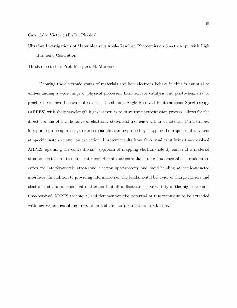
Knowing the electronic states of materials and how electrons behave in time is essential to
understanding a wide range of physical processes, from surface catalysis and photochemistry to
practical electrical behavior of devices. Combining Angle-Resolved Photoemission Spectroscopy
(ARPES) with short wavelength high-harmonics to drive the photoemission process, allows for the
direct probing of a wide range of electronic states and momenta within a material. Furthermore,
in a pump-probe approach, electron dynamics can be probed by mapping the response of a system
at specific instances after an excitation. I present results from three studies utilizing time-resolved
ARPES, spanning the conventional” approach of mapping electron/hole dynamics of a material
after an excitation - to more exotic experimental schemes that probe fundamental electronic prop-
erties via interferometric attosecond electron spectroscopy and band-bending at semiconductor
interfaces. In addition to providing information on the fundamental behavior of charge carriers and
electronic states in condensed matter, such studies illustrate the versatility of the high harmonic
time-resolved ARPES technique, and demonstrate the potential of this technique to be extended
with new experimental high-resolution and circular-polarization capabilities.

Dedication
For Jing.

v
Acknowledgements
This work is the result of the teaching, mentoring, collaboration, patience, and drive of many
great people. I especially thank my advisors, Margaret and Henry, for awarding me incredible
opportunities, academically and professionally, and having unwavering patience in the construction
of a new experiment. I am also grateful to have traveled and collaborated with some of the best
mentors and minds in the surface science community: Martin Aeschlimann (TU Kaiserslautern)
and Michael Bauer (TU Kiel), Dan Dessau (CU Boulder), and Mark Keller (NIST). Thank you
to my mentors at IBM, especially Richard Haight, who has been a pioneer in this field from its
beginning and whose perspectives on science and life have been invaluable.
I have had the pleasure of working with two incredibly talented post-docs during my tenure.
Stefan Mathias, who implemented the initial apparatus that ours currently resembles, has been a
great personal and professional mentor. This experiment would not be possible without his expertise
and courage to tear everything down and start anew. Piotr Matyba has been a great contribution
in offering fresh perspectives and ideas for experiments. He has had tremendous patience and
diligence in seeing the experiment finally produce results and it could not have been done without
him. Thank you to the PES team: Cong Chen and Zhensheng Tao. The experiment is in excellent
hands with their direction and there is assuredly more great science to come.
Jing, this should have been your work. Im sad others wont get to experience late nights in
lab laughing about horrible mistranslations in Chinese. Ethan, Ive been trying to incorporate your
fantastical view of the world and love for adventure. Thank you for giving me the best motivational
speech still ringing in my head: “Go team!” I miss you both tremendously.
vi
I gratefully acknowledge support from the JILA staff, especially the instrument shop staff:
Hans Green, Blaine Horner, Todd Asnicar, Kim Hagen, Tracy Keep, Dave Alchenberger, and Kels
Detra. The realization of the constant redesigns to this experiment would not have been possible
without their fined tuned expertise. To the JILA computing team, especially JR Raith who should
be given a cape for his superhero ability to always have the right replacement part at 8pm or know
exactly which commands to execute when the Windows machines decide to rebel.
To the Kaiserslautern crew: especially Steffen Eich, Sebastian Emmerich, Jurij Urbancic,
Andy Ruffing, and Martin Wiesenmayer. Thank you for making the late night runs way more fun
than they should be and education on all things definitively “German”. Thank you to the past
(esp. Luis Miaja-Avila, Daisy Raymondson, Sterling Backus) and present KM group members.
To Eric, Kevin, Steve, Carrie, Travis, Joe, Jrr, Dan H., Alejandra, Andrew, Dan W., Katie
and Phoenix who are the best support to my sanity. To my roommate here for 6 years, Tara Drake,
who amazingly shares my love of all things ridiculous and is always able to help with late night
existential crises. You are the best person to laugh with about science not making any sense. Thank
you to Craig Hogle, for much needed dance interludes, coffee breaks, stories, and introduction to
horrible, horrible songs that should not be listened to by anyone.
To my Dad- who taught me that everything is a “project”, nothing is ever a “black box”,
and not to fear taking things apart (while having a few choice swears reserved in case things go
wrong). To my Mom- who instilled curiosity and constant reminders that the world is a really,
really big place to explore. To my big brother, Jake- who is the beautiful dichotomy of being the
constant voice of pragmatism while having airplane/drag racing/boar hunting hobbies that make
me scared just how relative the term “pragmatism” can be. You are a great support and thanks
for reminding me that its ok to have fun occasionally.
Finally, Yance. I 100% would have been unable to do this without you. 9 years and always
willing to talk science, horrible tv shows (even if you spoil the ending to them all), philosophy,
games, and life. After 2 states, 5 houses, innumerable cross country flights, and the inevitable 4
ER visits (Im really sorry Im such a clutz), thank you for being the best copilot on this adventure.
vii
Contents
Chapter
1 Introduction 1
1.1 Organization of thesis . . . . . . . . . . . . . . . . . . . . . . . . . . . . . . . . . . . 6
2 General Theoretical Background 7
2.1 Photoemission Spectroscopy . . . . . . . . . . . . . . . . . . . . . . . . . . . . . . . . 7
2.1.1 Angle Resolved Photoemission . . . . . . . . . . . . . . . . . . . . . . . . . . 10
2.1.2 Photoemission: Three step model vs one step model . . . . . . . . . . . . . . 12
2.2 High Harmonic Generation . . . . . . . . . . . . . . . . . . . . . . . . . . . . . . . . 14
2.2.1 Semi-Classical Model . . . . . . . . . . . . . . . . . . . . . . . . . . . . . . . . 15
2.2.2 HHG Characteristics . . . . . . . . . . . . . . . . . . . . . . . . . . . . . . . . 20
2.2.3 Phase Matching in a Capillary Waveguide . . . . . . . . . . . . . . . . . . . . 22
2.3 Advantages of pairing High Harmonics with Photoemission . . . . . . . . . . . . . . 24
2.3.1 Accessible Momentum Range . . . . . . . . . . . . . . . . . . . . . . . . . . . 24
2.3.2 Surface Sensitivity . . . . . . . . . . . . . . . . . . . . . . . . . . . . . . . . . 25
2.3.3 Background Separation . . . . . . . . . . . . . . . . . . . . . . . . . . . . . . 27
3 Experimental Apparatus and Techniques 29
3.1 Ti:Sapphire Oscillator & Amplifier . . . . . . . . . . . . . . . . . . . . . . . . . . . . 29
3.2 Beamline . . . . . . . . . . . . . . . . . . . . . . . . . . . . . . . . . . . . . . . . . . 33
3.2.1 EUV Beamline . . . . . . . . . . . . . . . . . . . . . . . . . . . . . . . . . . . 33
viii
3.2.2 IR Beamline . . . . . . . . . . . . . . . . . . . . . . . . . . . . . . . . . . . . 42
3.2.3 IR Pump Temporal Compression . . . . . . . . . . . . . . . . . . . . . . . . . 42
3.3 UHV Chamber . . . . . . . . . . . . . . . . . . . . . . . . . . . . . . . . . . . . . . . 45
3.3.1 Sample Preparation Tools . . . . . . . . . . . . . . . . . . . . . . . . . . . . . 46
3.3.2 Sample Characterization Tools . . . . . . . . . . . . . . . . . . . . . . . . . . 47
3.4 ARPES Detector . . . . . . . . . . . . . . . . . . . . . . . . . . . . . . . . . . . . . . 48
3.4.1 Lens System . . . . . . . . . . . . . . . . . . . . . . . . . . . . . . . . . . . . 49
3.4.2 Hemispherical Analyzer . . . . . . . . . . . . . . . . . . . . . . . . . . . . . . 49
3.4.3 Electron Detection . . . . . . . . . . . . . . . . . . . . . . . . . . . . . . . . . 51
3.5 Custom Cryogenic Cooling Manipulator and Sample Holder . . . . . . . . . . . . . . 51
3.6 Finding spatial and temporal overlap . . . . . . . . . . . . . . . . . . . . . . . . . . . 55
3.7 Future Improvements . . . . . . . . . . . . . . . . . . . . . . . . . . . . . . . . . . . . 57
4 Two-Photon Photoelectron Interferometry on Cu(111) 59
4.1 Theoretical Background . . . . . . . . . . . . . . . . . . . . . . . . . . . . . . . . . . 60
4.1.1 Single EUV Harmonic . . . . . . . . . . . . . . . . . . . . . . . . . . . . . . . 61
4.1.2 Multiple Harmonics- RABITT . . . . . . . . . . . . . . . . . . . . . . . . . . 64
4.1.3 Previous Attosecond Studies on Surfaces . . . . . . . . . . . . . . . . . . . . . 69
4.2 RABITT on Surfaces . . . . . . . . . . . . . . . . . . . . . . . . . . . . . . . . . . . . 72
4.2.1 Surface States . . . . . . . . . . . . . . . . . . . . . . . . . . . . . . . . . . . . 72
4.2.2 Cu(111) Band structure . . . . . . . . . . . . . . . . . . . . . . . . . . . . . . 74
4.3 Experimental Configuration . . . . . . . . . . . . . . . . . . . . . . . . . . . . . . . . 74
4.4 Experimental Results . . . . . . . . . . . . . . . . . . . . . . . . . . . . . . . . . . . . 76
4.5 Discussion . . . . . . . . . . . . . . . . . . . . . . . . . . . . . . . . . . . . . . . . . . 80
4.6 Conclusions . . . . . . . . . . . . . . . . . . . . . . . . . . . . . . . . . . . . . . . . . 83
5 Graphene 84
5.1 Theoretical description . . . . . . . . . . . . . . . . . . . . . . . . . . . . . . . . . . . 85

ix
5.2 Graphene on different substrates . . . . . . . . . . . . . . . . . . . . . . . . . . . . . 88
5.3 Dynamical Investigations . . . . . . . . . . . . . . . . . . . . . . . . . . . . . . . . . 90
5.4 Chapter Organization . . . . . . . . . . . . . . . . . . . . . . . . . . . . . . . . . . . 91
5.5 SiC/ Graphene . . . . . . . . . . . . . . . . . . . . . . . . . . . . . . . . . . . . . . . 91
5.5.1 Sample Preparation . . . . . . . . . . . . . . . . . . . . . . . . . . . . . . . . 92
5.5.2 Time resolved Measurements . . . . . . . . . . . . . . . . . . . . . . . . . . . 94
5.6 Ni(111)/Graphene . . . . . . . . . . . . . . . . . . . . . . . . . . . . . . . . . . . . . 97
5.6.1 Sample Preparation . . . . . . . . . . . . . . . . . . . . . . . . . . . . . . . . 100
5.6.2 Intercalation of Alkali Atoms . . . . . . . . . . . . . . . . . . . . . . . . . . . 104
5.6.3 Discussion and Conclusions . . . . . . . . . . . . . . . . . . . . . . . . . . . . 112
6 Band bending Studies on InGaAs/high-k/metal Gate Stacks 115
6.1 Technical Background . . . . . . . . . . . . . . . . . . . . . . . . . . . . . . . . . . . 118
6.1.1 Band Flattening Technique . . . . . . . . . . . . . . . . . . . . . . . . . . . . 119
6.1.2 C-V/I-V Characterizations . . . . . . . . . . . . . . . . . . . . . . . . . . . . 121
6.2 Experimental Configuration . . . . . . . . . . . . . . . . . . . . . . . . . . . . . . . . 123
6.3 Surface Cleaning Investigations on InGaAs using Activated Hydrogen . . . . . . . . 125
6.4 Results and Discussion . . . . . . . . . . . . . . . . . . . . . . . . . . . . . . . . . . . 126
6.4.1 Stack Deposition Studies . . . . . . . . . . . . . . . . . . . . . . . . . . . . . 126
6.4.2 Thermal Treatment of stacks . . . . . . . . . . . . . . . . . . . . . . . . . . . 128
6.4.3 C-V/ I-V Characterizations . . . . . . . . . . . . . . . . . . . . . . . . . . . . 131
6.5 Conclusions . . . . . . . . . . . . . . . . . . . . . . . . . . . . . . . . . . . . . . . . . 133
7 Future Outlook and Conclusions 134
7.1 Circular harmonic Generation . . . . . . . . . . . . . . . . . . . . . . . . . . . . . . . 134
7.1.1 RABITT studies on Cu(111) . . . . . . . . . . . . . . . . . . . . . . . . . . . 136
7.1.2 Graphene . . . . . . . . . . . . . . . . . . . . . . . . . . . . . . . . . . . . . . 137
7.1.3 Topological Insulators . . . . . . . . . . . . . . . . . . . . . . . . . . . . . . . 138

x
7.1.4 Surface-Adsorbate Systems . . . . . . . . . . . . . . . . . . . . . . . . . . . . 138
7.2 Time-resolved High energy-resolution Studies . . . . . . . . . . . . . . . . . . . . . . 139
7.2.1 Directly resolving interface states in InGaAs . . . . . . . . . . . . . . . . . . 139
7.3 Conclusion . . . . . . . . . . . . . . . . . . . . . . . . . . . . . . . . . . . . . . . . . 140
Bibliography 141
Appendix
A Supplemental Material 166
A.1 Multilayer Mirror Characterization and Coatings . . . . . . . . . . . . . . . . . . . . 166
A.2 1ω Optical interference unique from RABITT effect . . . . . . . . . . . . . . . . . . 167
A.3 Surface Emission from Cu(111) in RABITT studies . . . . . . . . . . . . . . . . . . . 168
A.4 Fourier Analysis Method- RABITT studies on Cu(111) . . . . . . . . . . . . . . . . . 169
A.5 Details of DFT and Bader Charge Analysis for Na intercalation on Gr/Ni(111) . . . 173

xi
Tables
Table
3.1 Amplifier Output energies with repetition rate . . . . . . . . . . . . . . . . . . . . . 32
3.2 Common harmonics with generation parameters, measured bandwidth for each har-
monic, and estimated flux . . . . . . . . . . . . . . . . . . . . . . . . . . . . . . . . . 36
3.3 Custom Sample holder temperature range performance . . . . . . . . . . . . . . . . . 52
xii
Figures
Figure
1.1 Timescales for dynamical processes determined via direct time-resolved measure-
ments or line-width analysis . . . . . . . . . . . . . . . . . . . . . . . . . . . . . . . . 2
2.1 Photoemission process energy diagram and sample work function measurement . . . 8
2.2 General illustration for photoemission from surfaces, with k⊥ and k|| components
and example ARPES spectra . . . . . . . . . . . . . . . . . . . . . . . . . . . . . . . 11
2.3 Illustration of Three-step photoemission model versus One-step model . . . . . . . . 13
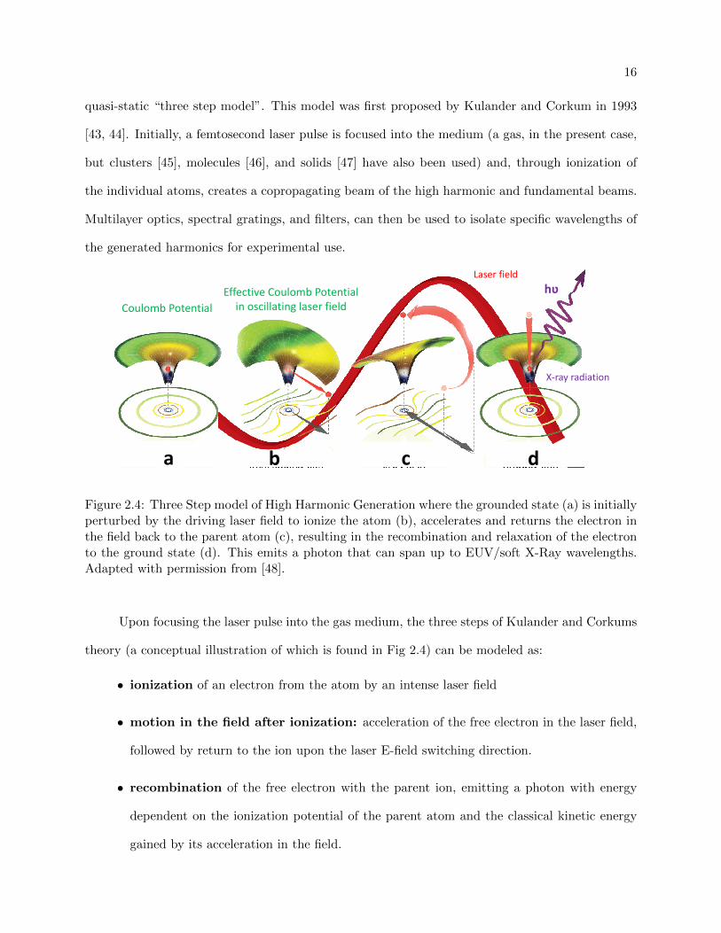
2.4 Three step model of High Harmonic Generation . . . . . . . . . . . . . . . . . . . . . 16
2.5 Potential ionization schemes for varying laser intensity . . . . . . . . . . . . . . . . . 18
2.6 Electron Trajectory for HHG recombination and peak Kinetic Energy gain vs laser
phase . . . . . . . . . . . . . . . . . . . . . . . . . . . . . . . . . . . . . . . . . . . . 19
2.7 ARPES Spectra using different photon energies & Emission angle as a function of
photon energy . . . . . . . . . . . . . . . . . . . . . . . . . . . . . . . . . . . . . . . . 25
2.8 Electron mean free path as a function of energy with experimental values . . . . . . 26
2.9 Photoemission spectra with inelastically scattered background using different photon
energies . . . . . . . . . . . . . . . . . . . . . . . . . . . . . . . . . . . . . . . . . . . 28
3.1 Chirped Pulse Amplifier layout and spectrum . . . . . . . . . . . . . . . . . . . . . . 30
3.2 Energy broadening due to electron-electron Coulomb effects . . . . . . . . . . . . . . 32
3.3 General Experimental Layout . . . . . . . . . . . . . . . . . . . . . . . . . . . . . . . 34
xiii
3.4 22 eV Harmonic ARPES spectra on Cu(111) showing 6 eV collection“”window” . . . 37
3.5 27th vs 7th harmonic spectra showing narrower harmonic bandwidth . . . . . . . . . 39
3.6 Mirror Chamber for Spectral and Non-spectral selection layouts . . . . . . . . . . . . 40
3.7 Calculation for optimal capillary length for SPM . . . . . . . . . . . . . . . . . . . . 43
3.8 SPM layout and retrieved FROG traces of input and output pulses . . . . . . . . . . 44
3.9 SPM spectra comparison of Ar, Kr, and Xe . . . . . . . . . . . . . . . . . . . . . . . 45
3.10 Electrostatic lens system for Angle-resolved electron detector . . . . . . . . . . . . . 50
3.11 energy and angular resolution for ARPES detector . . . . . . . . . . . . . . . . . . . 50
3.12 Sample Holder Design Iterations . . . . . . . . . . . . . . . . . . . . . . . . . . . . . 53
3.13 Cross correlation for IR pump- IR probe multiphoton ionization . . . . . . . . . . . . 56
3.14 Fermi mapping of materials with additional sample manipulator rotation . . . . . . . 58
4.1 Photoelectron distribution depending on EUV pulse length with IR field modulation 61
4.2 General description of RABITT method . . . . . . . . . . . . . . . . . . . . . . . . . 65
4.3 Wigner and Continuum- Continuum delay contributions to atomic delay . . . . . . . 69
4.4 Experimental Setup for RABITT experiment on multiple states in Cu(111) . . . . . 73
4.5 Representative electronic band structure for conduction and surface band structure 75
4.6 RABITT photoemission data when the HHG and infrared fields are and are not
overlapped in time . . . . . . . . . . . . . . . . . . . . . . . . . . . . . . . . . . . . . 77
4.7 RABITT traces for the surface state region and non-surface state region of Cu(111) 79
4.8 RABITT extracted phases for conduction band and surface state electrons . . . . . . 81
5.1 Graphene orbitals and real/ reciprocal lattice . . . . . . . . . . . . . . . . . . . . . . 86
5.2 Graphene Band structure . . . . . . . . . . . . . . . . . . . . . . . . . . . . . . . . . 88
5.3 Si-face and C-face Graphene band structure . . . . . . . . . . . . . . . . . . . . . . . 93
5.4 Time resolved difference map for electron and hole dynamics in SiC graphene . . . . 95
5.5 Electron/hole dynamics with extracted electronic temperature for SiC-graphene . . . 96
5.6 Top and side view of graphene/Ni(111) lattice with orbital coupling representation . 98

xiv
5.7 Graphene/Ni(111) band structure- experimental and DFT calculated . . . . . . . . . 99
5.8 LEED and Magnetic Force Microscopy of Ni(111) sample . . . . . . . . . . . . . . . 101
5.9 ARPES spectra for Mono and Bilayer Graphene/Ni(111) . . . . . . . . . . . . . . . . 102
5.10 Work function of Na/Graphene surface with dosing time . . . . . . . . . . . . . . . . 103
5.11 ARPES for surface adsorbed and intercalated Na on Graphene/Ni(111) after O2
exposure . . . . . . . . . . . . . . . . . . . . . . . . . . . . . . . . . . . . . . . . . . . 106
5.12 ARPES during Na intercalation on Graphene/Ni(111) . . . . . . . . . . . . . . . . . 109
5.13 DFT calculated band structure for adsorption and intercalation of Na on Graphene/
Ni(111) . . . . . . . . . . . . . . . . . . . . . . . . . . . . . . . . . . . . . . . . . . . 110
5.14 Bader charge analysis for charge density accumulation/depletion upon Na intercalation111
6.1 Classic n-channel MOSFET layout and evolution of transistor gate length over time 116
6.2 Band Diagram for p-type MOS capacitor at zero and applied bias . . . . . . . . . . . 119
6.3 Banding flattening technique using femtosecond pump-probe spectroscopy . . . . . . 120
6.4 C-V measurement technique and corresponding band diagrams under accumulation,
flatband, depletion, and inversion . . . . . . . . . . . . . . . . . . . . . . . . . . . . . 122
6.5 Experimental setup for band flattening studies . . . . . . . . . . . . . . . . . . . . . 124
6.6 XPS studies on the effects of Activated Hydrogen cleaning for bare InGaAs surfaces 125
6.7 Measured interfacial Fermi level for n & p-type bare InGaAs, InGaAs/high-k, and
InGaAs/high-k/TiN, shown for both Al2O3 and HfO2 . . . . . . . . . . . . . . . . . 127
6.8 annealing temperature vs interfacial Fermi level for metal/non-metal gated stacks . . 129
6.9 Work function vs annealing temperature for Al2O3 stacks . . . . . . . . . . . . . . . 130
6.10 C-V characterization for p-type and n-type InGaAs/4 nm high-κ/5nm TiN stacks
with Al2O3 and HfO2 . . . . . . . . . . . . . . . . . . . . . . . . . . . . . . . . . . . 132
7.1 Classic n-channel MOSFET layout and evolution of transistor gate length over time 135

xv
A.1 Multilayer mirror reflectivity and corresponding multilayer material shown with op-
timal photon energy range . . . . . . . . . . . . . . . . . . . . . . . . . . . . . . . . . 167
A.2 Multiphoton ionization as a function of delay showing 1 ω oscillation period . . . . . 167
A.3 Generated interfering sidebands under High IR intensities and with contaminated
surfaces . . . . . . . . . . . . . . . . . . . . . . . . . . . . . . . . . . . . . . . . . . . 168
A.4 k⊥ dispersion for sp and d states over the harmonic comb . . . . . . . . . . . . . . . 169
A.5 Photoemission spectrum of Cu(111) with denoted integration regions and extracted
EDC . . . . . . . . . . . . . . . . . . . . . . . . . . . . . . . . . . . . . . . . . . . . . 170
A.6 Average cross-spectral density power for the sp band and surface state . . . . . . . . 171
A.7 coherence function for the sideband feature . . . . . . . . . . . . . . . . . . . . . . . 172
Chapter 1
Introduction
One of the key motivations in the field of Material Science has been in determining precisely
how a material’s underlying structure- meaning geometric and, by extension, electronic- dictates
its macroscopic properties and behavior. For example, a material’s electrical conductivity is largely
determined by its electronic structure, with metals and semiconductors having larger conductivity
than insulators due to the increased mobility of their charge carriers. The chemical reactivity
of a surface is dictated by the electronegativity and dangling bonds of the atoms or molecules
terminating it. A material’s electronic structure- whether probed at a surface, interface, or within
the bulk- encapsulates these characteristics and can inform on these macroscopic properties.
Of particular interest is the local electronic structure at surfaces and interfaces. Surfaces
serve as the primary stage for processes like adsorption, desorption, diffusion, and surface-assisted
chemical reactions (ie surface catalysis and surface photochemistry). This is evident in everyday
applications like the Platinum-mediated redox reaction used in modern automobile catalytic con-
verters, reducing CO pollution. Electronic structure and carrier transport through interfaces is also
vital to the function and operating characteristics of electronic and opto-electronic devices, from
transistors to photovoltaics. Considerable effort has therefore been made at being able to probe
this local electronic structure. Understandably, one of the most direct methods in which to do this
is to probe the energy states of the electrons directly, “mapping” the energy levels (E) and, in
well-defined crystalline structures, crystalline momentum (k) at the surface of the material through
a method like photoemission spectroscopy. In photoemission, the energy of detected electrons can
2
be related back to the energy state from which it came, allowing the direct “imaging” of electronic
band structure in materials.
Petek and Ogawa, Prog Surf. Sci. 56, 237 (1997)
relate
Structure to Function
Motivation: Study electron dynamics with femtosecond resolution
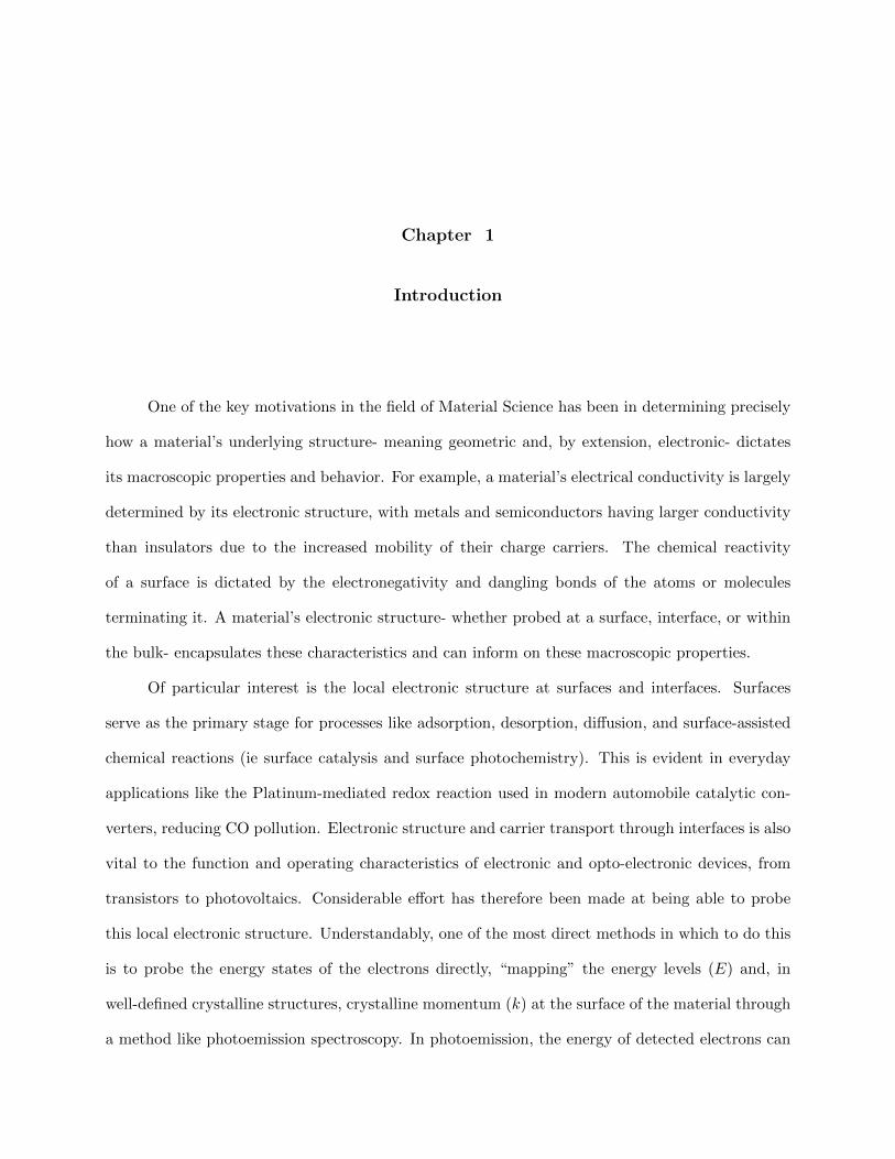
Figure 1.1: Timescales for dynamical processes determined via direct time-resolved measurementsor line-width analysis. Dynamical screening of the incident external laser field occurs on the shortesttimescales, followed by dephasing of coherent excitations (seen in metals). The original nonthermaldistribution of electrons/holes relaxes quickly to a Fermi-Dirac distribution via electron-electron(hole-hole) scattering, followed by slow electron-phonon scattering and resulting in heating of theoverall lattice. From presentation by M. Wolf, originally adapted with permission from [1].
The majority of the examples given above deal with reactions and processes at surfaces.
Interest in understanding processes necessarily means understanding of the process as it evolves
in time. In particular, the excitation and relaxation dynamics of the carriers in a material are
important for understanding properties like ablation in optical material processing [2], magneto-
optical recording [3], photochemical reactions [4], superconductivity, anomalous skin effect [5], etc.
The timescales in which these dynamics occur tend to depend on the fundamental scattering and
interaction of electrons, phonons, and spins of the particular system. In mapping out the response
of a system to an external perturbation, like an optical laser pulse, different physical processes
are dominant on varying timescales- picoseconds for electron-phonon mediated diffusion, ten to
hundreds of femtoseconds for electron interactions, and even down to the attosecond realm for
core hole relaxation and electron screening [1, 6]. Experiments have been able to determine these
3
dominant timescales through either direct time-resolved studies, sequentially probing a system
at snapshots in time after an initial excitation, or indirectly through linewidth measurements of
spectral features, where the Energy-time bandwidth limit (∆E∆t ∼ 4.14 in eV and fs for Gaussian
pulses [1]) sets an upper limit on the timescale of a process. A general illustration of these timescales,
with electronic-dominated processes characterized by short timescales and heavy nuclear motions
by longer timescales, is shown in Figure 1.1. Due to inhomogeneous broadening mechanisms in
spectroscopic lineshapes being difficult to fully account for [7], direct time-domain studies are
preferable. The timescales of these mechanisms are even seen to dictate reaction pathways of some
surface-mediated chemical reactions. One notable example is the case of CO coadsorbed with
O on a Ru(111) surface, where an initial 100 fs IR pulse can excite a hot electron population,
overcoming the chemical activation barrier to form CO2 and subsequently desorbing from the
surface. At longer timescales, electron-phonon scattering yields a thermally excited CO population
that, with insufficient energy to overcome the activation barrier for CO2 formation, simply desorbs
as CO [8]. The ability for electron-mediated vs phonon-mediated processes to dictate macroscopic
properties like which products result from a chemical reaction underscores the need to understand
the timescales in which they occur.
In order to study these dynamics, a probe is needed that acts on similar or faster timescales
than the processes we want to capture. This is akin to using a fast shutter speed on a camera
when capturing fast moving objects. Traditional radiation sources for photoemission spectroscopy
have been continuous-illumination plasma discharge lamps or 10-100 ps pulse-length synchrotron
facilities- neither is well suited for capturing the fastest dynamics that we’re interested in (c.f. Fig
1.1). Short pulse lasers capable of readily producing pulselengths of 10s of femtoseconds have be-
come increasingly available, with a number of companies now selling off-the-shelf products. With
nonlinear techniques and tricks in its generation, groups have even demonstrated isolated attosec-
ond pulses down to 67 as [9], with 140 as pulses used in time resolved spectroscopies [10]. Nonlinear
conversion techniques of these short-pulse lasers can be used to produce laser-driven high harmon-
ics from the vacuum UV to soft x-ray region [11, 12]. More commonly generated in the 10-100
4
eV range due to higher flux, these high harmonics provide a suitable photon source to be used
in photoemission studies, enabling a wider range of momentum and energy to be probed while
maintaining short pulses fit for time-resolved studies [13, 14]. First demonstrated in carrier dy-
namics studies in semiconductors like GaAs(110) [15], this EUV laser-based technique has since
been successfully used to study dynamics including femtosecond surface chemistry processes [16],
metal-insulator phase transitions [17], and transient charge screening in semiconductors [18]. Other
work in time resolved photoemission studies has recently focused on the generation of tunable ∼6
eV sources to improve the lower energy resolution that often is a consequence of the necessarily
broad bandwidth needed for the high harmonic generation process [19, 20]. As such, current efforts
to improve energy resolution of higher energy harmonics (21 eV) using blue-driven harmonics [14]
will be briefly discussed in this work. It should be noted that successful work has also been done
at the newly-available Free Electron Laser (FEL) facilities [21], where EUV emission is produced
via electrons accelerated to relativistic speeds using linear accelerators. These facilities have only
recently been implemented in time resolved experiments [22, 23] and show promise for future solid
state studies.
With the field of time-resolved photoemission spectroscopy still being highly explored, these
“traditional” time-resolved techniques have been recently extended to different geometries and ap-
plications. Most notably, with the demonstration of attosecond pulse trains and isolated attosecond
pulses using high harmonic generation schemes, attosecond spectroscopy has emerged as a ripe new
field of interest for dynamical investigations of materials. This holds promise for in-depth studies
of the fastest electron dynamics including inner shell relaxation dynamics, electron screening, and
electron-electron processes [24]. Initially applied to atomic systems and only recently extended
to solids, a common trait seen in these investigations has been the observation of phase delays
when comparing spectra of different electronic states within the atom or solid. Modeling of these
phase delays and interpretation of why they arise has proved challenging, with classical and quan-
tum mechanical models trading-off being able to reproduce experimental observations, with little
agreement and constant debate underway.
5
While the carrier dynamics on the femtosecond and attosecond timescales are important
to study, the hot-carrier population generated as a consequence of our laser-based time-resolved
technique can itself be used to measure band-bending in semiconductor systems. In traditional
“photovoltage” techniques [25, 26, 27], a moderate electron-hole population partially screens the
original dipole that is the cause of band bending at the semiconductor interface. The absolute
band bending, therefore, needs to be determined via extrapolating the screening effect over time.
With the large electron-hole population and high photon energy probes utilized in our experimental
approach, this screening effect can be pushed to saturation [28, 29], canceling out the dipole all
together and allowing the band bending to be directly probed. This technique can serve as a
powerful probe for measuring minor changes to this dipole, namely changes in the total number of
detrimental charge defects present that can effect the overall properties of the material when used
in devices [30, 31].
In the following work, an array of studies are performed with high harmonic time-resolved
photoemission spectroscopy that incorporate these conventional and alternative techniques. The
specific technical implementations range from the “traditional” ultrafast mapping of carrier dy-
namics to more recent extensions of this technique to the field of attosecond spectroscopy and
band-flattening measurements at semiconductor interfaces. While the well studied Cu(111) sur-
face is used in our attosecond spectroscopy measurements to make fundamental investigations of
attosecond delays of valence states, the later two materials investigated- graphene and InGaAs mul-
tilayer stacks- are of interest in the realm of “post-silicon” electronics. These materials are strong
candidates hoping to replace the increasingly-failing silicon in devices such as diodes, transistors,
and photovoltaics. In studies on graphene, carrier dynamics and controllable modifications of its
electronic structure via surface adsorbates are probed. Lastly, deposition and thermal annealing
studies on InGaAs multilayer stacks are used to determine the evolution of defects and trapped
charge through observing changes to the overall band bending at the semiconductor interface.
6
1.1 Organization of thesis
In Chapter 2, the relevant theoretical background will be presented on the techniques common
to all experiments presented within the work- namely photoemission spectroscopy, high harmonic
generation and the advantages that come with pairing them together. Chapter 3 outlines the ex-
perimental apparatus in its current form, describing the laser system, spectroscopic detector, and
sample preparation/ characterization tools. Modifications to this layout are noted in each respective
experimental chapter. Chapter 4 discusses interferometric attosecond spectroscopy, where the inter-
ferometric attosecond spectroscopy technique utilizing multiple harmonics is extended to surfaces
for the first time. By comparing the resulting interferometric signals of two unique valence states
in Cu(111), the nature of the observed phase delay is discussed in the context of current theoretical
models. Chapters 5-6 then probe two technologically relevant materials in detail- graphene (Gr) and
InGaAs multilayer stacks. In Chapter 5, carrier dynamics studies are performed on Gr/SiC(0001).
Alkali intercalation studies on Gr/Ni(111) are also presented. In Chapter 6, InGaAs/high-k/metal
gate stacks are probed with the band flattening photovoltage technique. Relevant theoretical de-
tails pertaining to each material and experiment will be presented in each respective experimental
chapter (Chapters 4-6). Future work including the recent realization of circular harmonics and
overall conclusions will be discussed in Chapter 7.
These results represent the culmination of a complete redesign of the previously existing ex-
periment, with past experimental capabilities being extended to include angularly-resolved electron
detection, a state-of-the-art sample manipulator, and an updated laser system for use with new
High Harmonic Generation (HHG) schemes. Further details of this redesign are left for discussion
in Chapter 3. The interfacial band-flattening measurements in Chapter 6 were performed using a
similar experimental apparatus during a research internship in the High-κ/metal gate Division at
IBM Yorktown Heights.
Chapter 2
General Theoretical Background
While the specific techniques vary in the experiments presented within this work, several
methods are common to all experiments. Primarily, all experiments utilize photoemission spec-
troscopy (PES) or angle resolved photoemission spectroscopy (ARPES) initiated with femtosecond
high-harmonic pulses, allowing the electronic states of a material to be probed directly. In a
time-resolved approach, these techniques can be implemented to study unfilled electronic states or
macroscopic phase changes in a material by electron excitation- “pumping” electrons into unfilled
bands or nonequilibrium states and subsequently “probing” them via photoemission.
The following sections outline the necessary theoretical background for these common tech-
niques that are employed in the experimental studies to follow. After providing the theoretical
description for PES (Section 2.1) and high harmonic generation (Sec 2.2), the specific advantages
of pairing HHG with PES are highlighted in Section 2.3.
2.1 Photoemission Spectroscopy
Photoemission spectroscopy has long been one of the most direct methods for studying elec-
tronic energy levels in solid state systems. First observed by Hertz in 1887 and explained by
Einstein in 1905 (see [32] and references therein), the photoelectric effect occurs when a photon is
incident on a medium, giving the possibility of emitting an electron. An electron can be emitted
with kinetic energy according to:
EK = hν − φm − EB (2.1)
8
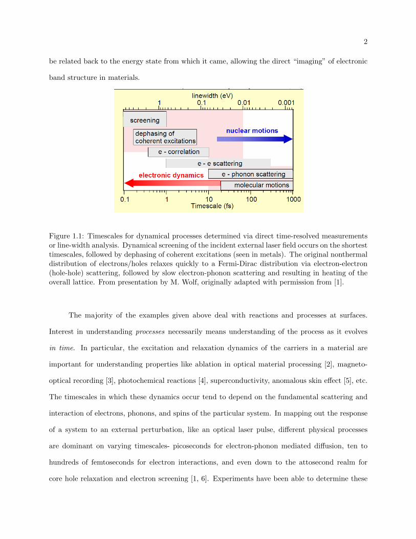
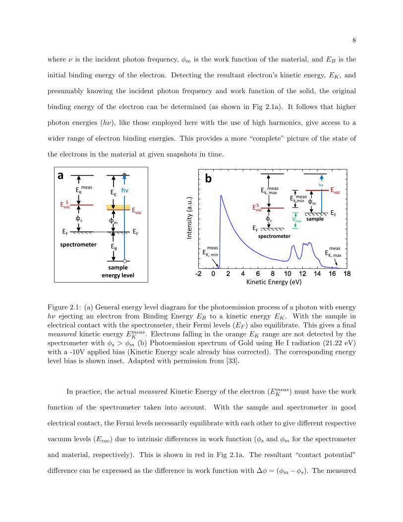
where ν is the incident photon frequency, φm is the work function of the material, and EB is the
initial binding energy of the electron. Detecting the resultant electron’s kinetic energy, EK , and
presumably knowing the incident photon frequency and work function of the solid, the original
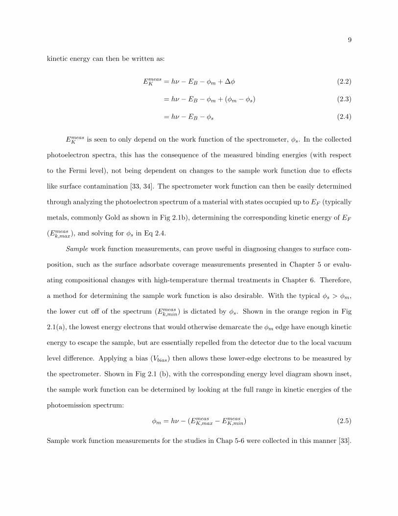
binding energy of the electron can be determined (as shown in Fig 2.1a). It follows that higher
photon energies (hν), like those employed here with the use of high harmonics, give access to a
wider range of electron binding energies. This provides a more “complete” picture of the state of
the electrons in the material at given snapshots in time.
EvacEvacS
EKEKmeas
φmφs
EF EF
EB
sampleenergy level
spectrometer
hν
a
Kinetic Energy (eV)
Intensity
(a.u.)
b
EK, min EK, maxmeas meas
EF
EF
Evac
EvacS
hνEk, max
meas
Ek,minmeas
Vbias sample
spectrometer
φs
φm
Figure 2.1: (a) General energy level diagram for the photoemission process of a photon with energyhν ejecting an electron from Binding Energy EB to a kinetic energy EK . With the sample inelectrical contact with the spectrometer, their Fermi levels (EF ) also equilibrate. This gives a finalmeasured kinetic energy EmeasK . Electrons falling in the orange EK range are not detected by thespectrometer with φs > φm (b) Photoemission spectrum of Gold using He I radiation (21.22 eV)with a -10V applied bias (Kinetic Energy scale already bias corrected). The corresponding energylevel bias is shown inset. Adapted with permission from [33].
In practice, the actual measured Kinetic Energy of the electron (EmeasK ) must have the work
function of the spectrometer taken into account. With the sample and spectrometer in good
electrical contact, the Fermi levels necessarily equilibrate with each other to give different respective
vacuum levels (Evac) due to intrinsic differences in work function (φs and φm for the spectrometer
and material, respectively). This is shown in red in Fig 2.1a. The resultant “contact potential”
difference can be expressed as the difference in work function with ∆φ = (φm−φs). The measured
9
kinetic energy can then be written as:
EmeasK = hν − EB − φm + ∆φ (2.2)
= hν − EB − φm + (φm − φs) (2.3)
= hν − EB − φs (2.4)
EmeasK is seen to only depend on the work function of the spectrometer, φs. In the collected
photoelectron spectra, this has the consequence of the measured binding energies (with respect
to the Fermi level), not being dependent on changes to the sample work function due to effects
like surface contamination [33, 34]. The spectrometer work function can then be easily determined
through analyzing the photoelectron spectrum of a material with states occupied up to EF (typically
metals, commonly Gold as shown in Fig 2.1b), determining the corresponding kinetic energy of EF
(Emeask,max), and solving for φs in Eq 2.4.
Sample work function measurements, can prove useful in diagnosing changes to surface com-
position, such as the surface adsorbate coverage measurements presented in Chapter 5 or evalu-
ating compositional changes with high-temperature thermal treatments in Chapter 6. Therefore,
a method for determining the sample work function is also desirable. With the typical φs > φm,
the lower cut off of the spectrum (Emeask,min) is dictated by φs. Shown in the orange region in Fig
2.1(a), the lowest energy electrons that would otherwise demarcate the φm edge have enough kinetic
energy to escape the sample, but are essentially repelled from the detector due to the local vacuum
level difference. Applying a bias (Vbias) then allows these lower-edge electrons to be measured by
the spectrometer. Shown in Fig 2.1 (b), with the corresponding energy level diagram shown inset,
the sample work function can be determined by looking at the full range in kinetic energies of the
photoemission spectrum:
φm = hν − (EmeasK,max − EmeasK,min) (2.5)
Sample work function measurements for the studies in Chap 5-6 were collected in this manner [33].
10
2.1.1 Angle Resolved Photoemission
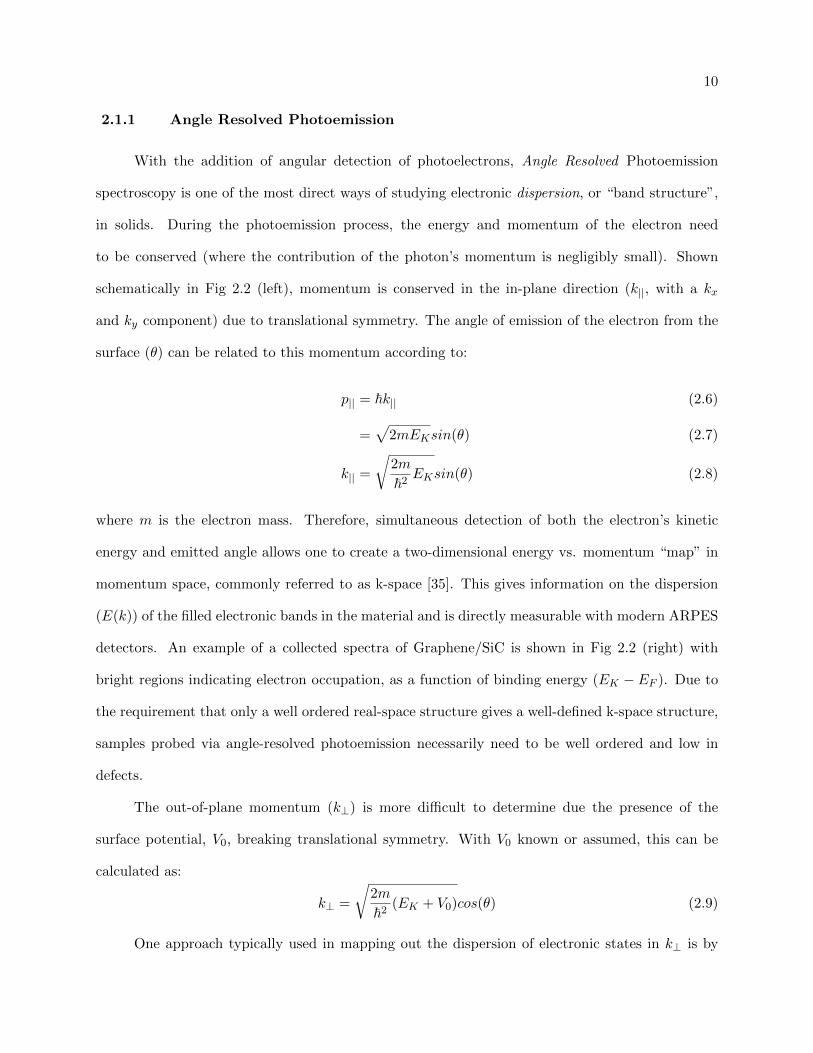
With the addition of angular detection of photoelectrons, Angle Resolved Photoemission
spectroscopy is one of the most direct ways of studying electronic dispersion, or “band structure”,
in solids. During the photoemission process, the energy and momentum of the electron need
to be conserved (where the contribution of the photon’s momentum is negligibly small). Shown
schematically in Fig 2.2 (left), momentum is conserved in the in-plane direction (k||, with a kx
and ky component) due to translational symmetry. The angle of emission of the electron from the
surface (θ) can be related to this momentum according to:
p|| = ~k|| (2.6)
=√
2mEKsin(θ) (2.7)
k|| =
√2m
~2EKsin(θ) (2.8)
where m is the electron mass. Therefore, simultaneous detection of both the electron’s kinetic
energy and emitted angle allows one to create a two-dimensional energy vs. momentum “map” in
momentum space, commonly referred to as k-space [35]. This gives information on the dispersion
(E(k)) of the filled electronic bands in the material and is directly measurable with modern ARPES
detectors. An example of a collected spectra of Graphene/SiC is shown in Fig 2.2 (right) with
bright regions indicating electron occupation, as a function of binding energy (EK − EF ). Due to
the requirement that only a well ordered real-space structure gives a well-defined k-space structure,
samples probed via angle-resolved photoemission necessarily need to be well ordered and low in
defects.
The out-of-plane momentum (k⊥) is more difficult to determine due the presence of the
surface potential, V0, breaking translational symmetry. With V0 known or assumed, this can be
calculated as:
k⊥ =
√2m
~2(EK + V0)cos(θ) (2.9)
One approach typically used in mapping out the dispersion of electronic states in k⊥ is by
11
kex
k ex
k||ex
kk
k||
z
θ
hν
T
T
0
0.5
‐1
‐1.5
1.71.6 1.8
Bind
ing Energy (e
V)
k||(Å‐1)
MDC
EDC
Figure 2.2: (left) General illustration for photoemission from surfaces upon illumination of photonwith energy hν, with k⊥ and k|| components identified for the photoelectron within the solid(k) and upon photoemission into the vacuum (kex. (right) typical ARPES spectra, shown forGraphene/Si(0001), with denoted energy distribution curve (EDC) and momentum distributioncurve (MDC) extracted along the blue and red lines, respectively.
varying the photon energy, but these types of measurements will not be employed in the studies
presented here. For the case of 2D materials, like graphene, k⊥ is zero and can be ignored in
dispersion considerations. As will be shown in Chapter 4, surface states are special electronic states
that also are only described by a k|| component, due to their wavefunction decaying exponentially
into the bulk.
One advantage of the ARPES technique is that it allows direct measurement of the single
particle spectral function of the solid, containing information on many-body interactions. In high
resolution studies, these quantities can be directly extracted from spectral linewidth measurements,
properly accounting for experimental broadenings [35]. In the studies presented here, the lineshape
of the collected spectral features is not analyzed in depth due to the dramatic energy broadening
due to the high harmonics. Our spectral linewidth is dictated by the temporally short pulses
required in the HHG process (∆E∆t > ~), necessitating a broad spectral bandwidth, as well as
non-ideal phase matching in the harmonic generation.
Typical ARPES distributions are usually represented in two ways:
12
• Energy Distribution Curves (EDCs): fixed (kx, ky) as a function of energy
• Momentum Distribution Curves (MDCs): fixed EB as a function of either kx or ky
Representative MDC and EDC curves are shown in Fig 2.2 (right), with the horizontal MDC lineout
shown in red and vertical EDC lineout shown in blue. The majority of distributions discussed in this
thesis will be looking at EDCs at a fixed value of k|| or integrated over a small range of k||. While
the bulk of the experimental results presented are collected using an angle-resolved photoelectron
detector, resulting in spectra similar to Fig 2.2 (right), the InGaAs experiments in Chapter 6 are
performed using a Time-of-flight detector. In this geometry, an electrostatic lens collects electrons
emitted over an angular acceptance range of ±20 from the surface normal. This gives an EDC
integrated over this entire angular acceptance and loses any dispersion information that one might
gain with angular detection.
2.1.2 Photoemission: Three step model vs one step model
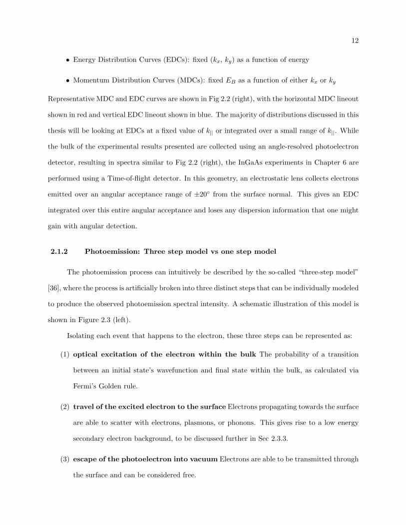
The photoemission process can intuitively be described by the so-called “three-step model”
[36], where the process is artificially broken into three distinct steps that can be individually modeled
to produce the observed photoemission spectral intensity. A schematic illustration of this model is
shown in Figure 2.3 (left).
Isolating each event that happens to the electron, these three steps can be represented as:
(1) optical excitation of the electron within the bulk The probability of a transition
between an initial state’s wavefunction and final state within the bulk, as calculated via
Fermi’s Golden rule.
(2) travel of the excited electron to the surface Electrons propagating towards the surface
are able to scatter with electrons, plasmons, or phonons. This gives rise to a low energy
secondary electron background, to be discussed further in Sec 2.3.3.
(3) escape of the photoelectron into vacuum Electrons are able to be transmitted through
the surface and can be considered free.
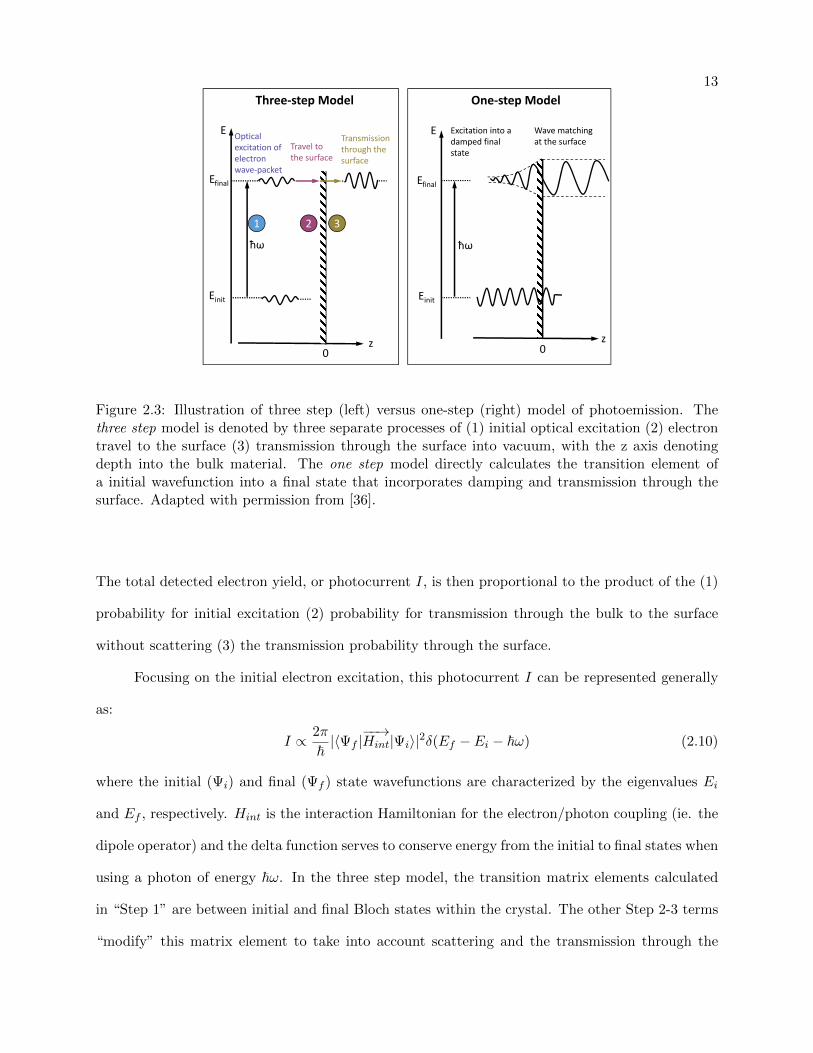
13
E
One‐step ModelThree‐step Model
E Excitation into adamped final state
Wave matching at the surfaceTransmission
through the surface
Travel to the surface
Optical excitation of electron wave‐packet
Efinal
Einit Einit
Efinal
ħω ħω
1 2 3
z z0 0
Figure 2.3: Illustration of three step (left) versus one-step (right) model of photoemission. Thethree step model is denoted by three separate processes of (1) initial optical excitation (2) electrontravel to the surface (3) transmission through the surface into vacuum, with the z axis denotingdepth into the bulk material. The one step model directly calculates the transition element ofa initial wavefunction into a final state that incorporates damping and transmission through thesurface. Adapted with permission from [36].
The total detected electron yield, or photocurrent I, is then proportional to the product of the (1)
probability for initial excitation (2) probability for transmission through the bulk to the surface
without scattering (3) the transmission probability through the surface.
Focusing on the initial electron excitation, this photocurrent I can be represented generally
as:
I ∝ 2π
~|〈Ψf |
−−→Hint|Ψi〉|2δ(Ef − Ei − ~ω) (2.10)
where the initial (Ψi) and final (Ψf ) state wavefunctions are characterized by the eigenvalues Ei
and Ef , respectively. Hint is the interaction Hamiltonian for the electron/photon coupling (ie. the
dipole operator) and the delta function serves to conserve energy from the initial to final states when
using a photon of energy ~ω. In the three step model, the transition matrix elements calculated
in “Step 1” are between initial and final Bloch states within the crystal. The other Step 2-3 terms
“modify” this matrix element to take into account scattering and the transmission through the
14
surface.
A more accurate “one-step model” [37] is to directly calculate the transition matrices from
an initial state to a damped final photoemitted state, shown in Fig 2.3 (right). In this manner, it
is able to incorporate the entirety of these three steps into a single Fermi’s Golden Rule transition
matrix with a more accurate choice of final states, already taking into account these scattering and
surface effects. The initial Bloch wavefunction is coupled to a damped final state wavefunction via
the dipole operator, where the damping of the final state incorporates the scattering probability for
the electron. This matrix element is, unsurprisingly, inherently difficult to evaluate and requires
a number of simplifications. Theoretical approaches trying to directly evaluate these transition
matrix elements are important for the attosecond measurements presented in Chapter 4, where the
observed phase delays can be related to the phase of the transition matrix element.
2.2 High Harmonic Generation
Development of EUV/Soft XRay laser sources with high spatial and temporal coherence is
greatly desired for solid state studies due to greater accessibility to momentum and energy states
and specific advantages offered when using the photoemission technique. However, such sources
have proved difficult to realize due to the tendency for most materials to be highly absorbing at
shorter wavelength than 200 nm. This makes production via traditional nonlinear crystals not
feasible and greatly limits the choice of material if used as a laser gain medium. In general, the
pump power required to produce a given output wavelength roughly scales as λ−5. This would
mean an output wavelength in the X-Ray region of 1 nm would already require Terawatt pump
power, making practical experimental implementation difficult [13].
Since its first observation in 1987 [38], High Harmonic Generation (HHG) has been one of
the most viable candidates for a versatile, compact source of EUV to Soft X-Ray light. In this
process, coherent visible light is nonlinearly upconverted to EUV and Soft X Ray wavelengths,
generating a comb of harmonics that ideally spans the entire spectrum between the fundamental
and the EUV/ X-Ray region. Due to the magnitude of the perturbation needed to the generating
15
medium’s Coulombic potential, this phenomena was only made possible on table-top scale with the
advent of ultrafast (sub-picosecond), high intensity (1015 to 1018 W/cm2) laser sources [38, 39].
Recent experimental work in improved generation regimes with long driving wavelengths (> 1 µm)
have been seen to generate wavelengths up to the keV regime [12].
Multiple sources exist for the generation of EUV-X-Ray light. Laser-driven high harmonic
generation is attractive for several reasons compared to other available sources like synchrotrons,
femtosecond slicing electron bunches, EUV lasers, and FELs. Several reviews overviewing the
benefits of femtosecond x-ray sources from synchrotrons, FELs, and tabletop sources are available
[40, 41] and only a brief comparison will be outlined here. EUV lasers that use a highly excited
gain medium generate a high photon flux, but are limited in wavelength to the lasing transition of
the generating medium. On the other hand, synchrotrons and FELs generate high intensity pulses
that are tunable in wavelength, making then flexible in experimental applications. However, due to
the physically large layouts of the apparatuses, control over the exact timing of the generated laser
pulses is difficult, introducing a temporal “jitter” that makes them unsuited for studies requiring
high temporal resolution. High Harmonic generation fits into this EUV/ X Ray source toolbox by
having its characteristics being dependent on the driving laser source. Used with a femtosecond laser
source like the Titanium-doped Sapphire (Ti:Saph) oscillator/amplifier system employed here, the
characteristic energy and temporal resolution offered are well suited for time-resolved photoemission
studies. The ability to pick from a range of generated harmonic wavelengths also allows for a wider
range of material applications. This combination of high spatial and temporal coherence with
favorable energy and temporal resolution on a continuously accessible tabletop source has become
an attractive technique increasingly used in high resolution photoemission static and dynamical
studies.
2.2.1 Semi-Classical Model
While a quantum mechanical description is needed to obtain an accurate model of high
harmonic generation [42], approximations can be made that allow for an intuitive semi-classical,
16
quasi-static “three step model”. This model was first proposed by Kulander and Corkum in 1993
[43, 44]. Initially, a femtosecond laser pulse is focused into the medium (a gas, in the present case,
but clusters [45], molecules [46], and solids [47] have also been used) and, through ionization of
the individual atoms, creates a copropagating beam of the high harmonic and fundamental beams.
Multilayer optics, spectral gratings, and filters, can then be used to isolate specific wavelengths of
the generated harmonics for experimental use.
a b c d
Coulomb PotentialEffective Coulomb Potentialin oscillating laser field
Laser field
X‐ray radiation
hʋ
Figure 2.4: Three Step model of High Harmonic Generation where the grounded state (a) is initiallyperturbed by the driving laser field to ionize the atom (b), accelerates and returns the electron inthe field back to the parent atom (c), resulting in the recombination and relaxation of the electronto the ground state (d). This emits a photon that can span up to EUV/soft X-Ray wavelengths.Adapted with permission from [48].
Upon focusing the laser pulse into the gas medium, the three steps of Kulander and Corkums
theory (a conceptual illustration of which is found in Fig 2.4) can be modeled as:
• ionization of an electron from the atom by an intense laser field
• motion in the field after ionization: acceleration of the free electron in the laser field,
followed by return to the ion upon the laser E-field switching direction.
• recombination of the free electron with the parent ion, emitting a photon with energy
dependent on the ionization potential of the parent atom and the classical kinetic energy
gained by its acceleration in the field.
17
With each step having an associated probability of occurrence, the total probability of occurrence
per atom can be calculated to predict the output intensity of each harmonic order. The details of
each of these processes will be discussed individually in the following sections.
2.2.1.1 Ionization
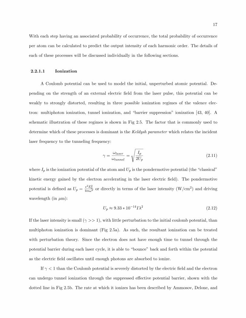
A Coulomb potential can be used to model the initial, unperturbed atomic potential. De-
pending on the strength of an external electric field from the laser pulse, this potential can be
weakly to strongly distorted, resulting in three possible ionization regimes of the valence elec-
tron: multiphoton ionization, tunnel ionization, and “barrier suppression” ionization [43, 40]. A
schematic illustration of these regimes is shown in Fig 2.5. The factor that is commonly used to
determine which of these processes is dominant is the Keldysh parameter which relates the incident
laser frequency to the tunneling frequency:
γ =ωlaserωtunnel
=
√Ip
2Up(2.11)
where Ip is the ionization potential of the atom and Up is the pondermotive potential (the “classical”
kinetic energy gained by the electron accelerating in the laser electric field). The pondermotive
potential is defined as Up =e2E2
04mω2 or directly in terms of the laser intensity (W/cm2) and driving
wavelength (in µm):
Up ≈ 9.33 ∗ 10−14Iλ2 (2.12)
If the laser intensity is small (γ >> 1), with little perturbation to the initial coulomb potential, than
multiphoton ionization is dominant (Fig 2.5a). As such, the resultant ionization can be treated
with perturbation theory. Since the electron does not have enough time to tunnel through the
potential barrier during each laser cycle, it is able to “bounce” back and forth within the potential
as the electric field oscillates until enough photons are absorbed to ionize.
If γ < 1 than the Coulomb potential is severely distorted by the electric field and the electron
can undergo tunnel ionization through the suppressed effective potential barrier, shown with the
dotted line in Fig 2.5b. The rate at which it ionizes has been described by Ammosov, Delone, and
18
Energy Energy Energy
positionposition position
a b c
Multi‐photon Ionization Tunnel Ionization Barrier Suppression Ionization
Figure 2.5: The three possible ionization potential schemes: a) multiphoton ionization b) tunnelionization c) barrier suppression ionization. The dashed curve represents the unperturbed Coulombpotential with the blue curve being the effective potential when including the driving laser field. Thehorizontal and vertical gray axes represent the position and binding energy, respectively. Adaptedwith permission from [40]
Krainov [49]. For the case of Argon (Ip = 15.76eV ) illuminated with a 800 nm pulse, this regime
is dominant for Ip > 1014 W/cm2. With laser intensities in the range 1014 − 1016 W/cm2, this
ionization process is dominant in most high harmonic generation schemes. Finally, for γ << 1,
the population of electrons in the ground state can be easily ionized since the effective potential is
suppressed below the ionization barrier (Fig 2.5c). This is barrier-suppression ionization.
2.2.1.2 Acceleration
Once ionized, the laser field intensity is much greater than the Coulomb potential and the
electron can be modeled as free to evolve in the field. Since the electron effectively has a continuum
of states available to it, it can be modeled classically instead of strictly quantum mechanically. The
electric field then has the form:
E(t) = E0cos(ωt)ex + αE0sin(ωt)ey (2.13)
where α represents the polarization of the fundamental light (0 for linear and ±1 for circularly),
E0 is the amplitude of the electric field, ω is the field frequency, and e is the unit vector denoted in
the x and y directions. Since the electron needs to eventually recombine with its parent ion, this
can only happen with α = 0, requiring our incident light to be linearly polarized when using one
19
driving field. The recent realization of circular harmonics [50], as explained further in Chapter 7,
can be achieved through the use of multiple driving fields. The equations of motion for the electron
can be obtained through solving ma = eE as:
vx(t) = eE0ωm sin(ωt) + v0x (2.14)
x(t) = − eE0ω2m
cos(ωt) + v0xt+ x0 (2.15)
vy(t) = −αeE0ωm cos(ωt) + v0y (2.16)
y(t) = −αeE0ω2m
sin(ωt) + v0yt+ y0 (2.17)
This assumes that the electron is at rest and at the origin once it tunnels through the potential
barrier since the displacement position after tunneling is small compared to its maximum deviation
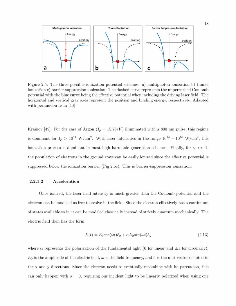
position from the atom (A vs nm). Only electrons released within a specific range of driving laser
phases (φ) will allow the electron to actually return to the parent atom. Plotting a range of electron
trajectories depending on the tunneling phase (shown in Figure 2.6a), one can see this only occurs
between 0− 90 degrees.
Time since tunneling (fs)
Electron
‐atom distance (a
0) φ = 0
π/2
π/4
π/6
φE field (π rad)
φE field (deg)
Kine
tic Ene
rgy (U
p)
0 0.1 0.2 0.3 0.4 0.5
0 20 40 60 800
1
2
3
~18⁰
~ 3.17 Up
a b
Figure 2.6: (a) plot of electron trajectory obtained from derived equations of motion (Eq 2.16). Thistrajectory is only ”closed”, returning to the ion (highlighted in red), when the electrons tunnels outbetween phases corresponding to 0−π/2 rad of the driving laser phase. (b) the kinetic energy gainversus the laser phase when the electron tunnels out of the potential. Adapted with permissionfrom [40]
The resultant final kinetic energy of the electron accelerating in the field depends on the
phase of the driving laser field at the time it tunnels out of the potential. Plotting the total kinetic
20
energy gain as a function of the driving electric field phase to find its maximum, this occurs at
∼ 18 and ∼ 3.17Up, as seen in Figure 2.6 b. If the electron evolves longer than this in the driving
field, it can either return 180 out of phase or after an even number of optical cycles, which has an
extremely low probability of occurrence.
2.2.1.3 Recombination
After gaining kinetic energy from accelerating in the laser field, the electron has a certain
probability to recombine with the parent ion and emit a photon equal to the energy having gained
in the field. For an accurate model, other scattering processes need to be considered such as elastic
scattering and collisional ionization. The total emission probability can be calculated via the
dipole operator, taking into account the associated phase. The maximum emitted photon energy
can be calculated via conservation of energy, where the amount of extra energy the electron has is
dependent on the ionization potential of the atom and the maximum energy that it is able to gain
from its evolution in the field:
hνmax = Ip + 3.17Up (2.18)
This serves as a maximum “cutoff” photon energy to our possible generated high harmonics [44].
2.2.2 HHG Characteristics
Without knowing anything of what the resultant spectrum looks like, some general observa-
tions can be made of what aspects of the process most drastically influence the overall harmonic
emission output. From looking at Eqs 2.18 and 2.12, the higest generated wavelength is depen-
dent on the laser peak intensity. Therefore, shorter laser pulses with higher peak intensity allow
for shorter cutoff wavelengths since the electron is allowed to “survive” for longer in the field (to
higher field strength) before ionizing. This allows it to gain more kinetic energy from the ponder-
motive force. Another dependent factor is the ionization potential of the atom. Higher ionization
potentials lead to higher cutoff frequencies. The influence of these two factors on the highest cutoff
photon energy can be seen when looking at atoms like Neon and Helium, with Ip = 21.6eV and
21
24.6eV respectively. With a 25 fs driving laser pulse width centered at 800nm and 6× 10¹⁵W/cm2
intensity, the highest harmonics possibly generated are the 163rd and 333rd (4.9nm and 2.4 nm
respectively). By comparison, with a longer 100 fs pulse width assuming the same peak intensity,
the cutoffs drop to the 119th and 237th harmonics for Neon and Helium, respectively [51].
Looking at the periodicity of the driving laser field, the HHG process also takes place every
half cycle of the driving field, producing a series of attosecond bursts. Therefore, only odd harmon-
ics are generated due to the odd symmetry of the generating process. To generate even harmonics,
a medium without inversion symmetry would be required, making the harmonic emission always
add constructively no matter if the photon is generated from the field oscillating one way or the
other. This does not exist for a gas. Introduction of a second pulse with a different fundamental
wavelength could generate the even pulses via filling in the gaps of the harmonic spectrum.
With the three step model as a general guide to the high harmonics generation process, the
resultant spectrum is seen to have three primary characteristics:
• An initial strong peak close to the fundamental wavelength
• A long plateau region with relatively equal intensity
• A sharp cutoff at high photon energies
In the time domain, HHG occurs every half cycle of the laser field in short attosecond bursts.
The initial strong peaks in the emission are where the generated intensity can be modeled by
perturbation theory. Relativity uniform intensity of the harmonics on the plateau are due to the
efficiency in ionization being “nonperturbative” and relatively independent of generated harmonic
order [43, 40]. In reality, these intermediate orders are not discretized. Since there are many
electron trajectories that contribute the each harmonic order, each contribution to the order has a
discrete frequency phase shift depending on when the emission of the HHG photon occurs. This
leads to an interference effect that somewhat “smears” out the orders. The sharp cut off is then
dictated by the limit in energy that an electron is able to gain from accelerating in the electric field
after ionization.
22
The decrease in signal intensity at high energies is due to the fact that only few electrons
contribute to such high generated energies since these electrons would be ionized near the peak of
the fundamental field. Also, due to this smaller number of electrons contributing to these orders,
the interference effects are not as drastic and the orders are more discretized. The overall conversion
efficiency of the entire process is typically on the order of 10−5 − 10−7 depending on the driving
wavelength [52, 12].
2.2.3 Phase Matching in a Capillary Waveguide
Up until now, certain assumptions have been made about the characteristics of the high
harmonic light generated in the gas, the main assumption being that the light generated from an
atom in one portion of the gas is exactly in phase with the light generated a certain distance later.
If this is not the case, then the harmonic light does not add coherently and the output intensity
is greatly reduced. If we are able to forcibly phase match our harmonic light, this corresponds to
a 102 to 103 factor increase in output intensity compared to the non-phase matched case, allowing
for greater experimental applications [53]. The characteristic length in which the phase of the
harmonically generated light “slips” from the phase of the fundamental phase by π is called the
coherence length and can vary from the mm scale for low (< 150eV ) photon energy to micrometer
scale for high (> 200eV ) photon energy. Maximizing this coherence length allows for greater
interaction length in which the harmonics are able to constructively interfere.
Several factors contribute to the spatial “phase mismatch” that needs to be corrected for
so that the output light is intense enough for practical applications. First, the gas in which the
harmonic light is generated is a nonlinear medium. As the light propagates, it inherently picks up
a phase lag such that:
Eq ∝∫ L
0Enf d(z)e−i∆kzdz (2.19)
propagating through a medium with length L where Eq is the electric field of the qth harmonic, n
is the order of the nonlinear process, d(z) is the nonlinear coefficient, ∆k is the phase mismatch
(∆k = qkf − kq) between the fundamental laser field wavevector, kf , and the harmonic field kq.
23
Thus, with a ∆k = 0, then the Eq is maximized, corresponding to a maximum in output intensity.
To see how much this effects the final intensity, this expression can be integrated assuming Enf and
d(z) are independent of propagation direction. This gives:
Eq ∝ L2sinc2(∆kL
2) (2.20)
With no phase mismatch, the output harmonic signal grows as L2, serving as a strong moti-
vation to try to make the mismatch zero. If ∆k is nonzero then it oscillates over the propagation
distance with the fields slipping in and out of constructive interference.
Seeing how strongly the phase mismatch effects the output intensity, several phase matching
approaches have been tried attempting to minimize ∆k. Expressing this mismatch more precisely,
three district components contribute to the overall phase difference:
∆ktotal = ∆kdisp + ∆kplasma + ∆kgeom (2.21)
where ∆kdisp is the dispersion due to propagation in the neutral gas medium, ∆kplasma is the plasma
dispersion from the plasma created from the unrecombined free carriers in the generating medium,
and ∆kgeom is the geometrical dispersion when confined. One of the most successful approaches
at minimizing ∆ktotal has been by using a gas-filled capillary waveguide. In this configuration, the
total ∆k expression can be written accounting for the inherent waveguide dispersion as:
∆ktotal = [n(ωf )− n(mωf )]ωfc
+ω2p(1−m2)
2mcωf+unl
2c(1−m2)
2ma2ωf(2.22)
where ωf is the fundamental laser frequency, n(ω) is the frequency dependent index of refraction of
the medium, m is the mth harmonic order, ωp is the plasma frequency, a is the inner radius of the
capillary and unl is the lth zero of the Bessel function Jn−l(unl) = 0 [40]. In general, the positive
dispersion of the index of refraction term kdisp can be made to cancel the negative dispersions of
the plasma (∆kplasma) and waveguide (∆kgeom). A final phase-matched harmonic signal can then
most easily be achieved by tuning the gas pressure within the capillary to adjust the density of the
neutral medium.
24
2.3 Advantages of pairing High Harmonics with Photoemission
Specific advantages are present in utilizing short wavelength high harmonics as the photon
source for the photoelectron process. In addition to simply being able to access a larger Binding
Energy range for the electrons within material, allowing more electronic states to be probed, sev-
eral secondary features allow for either greater characterization of the electronic states or better
discrimination of the photoelectron signal compared to utilizing longer wavelengths. Each of the
experiments presented in Chapters 4-6 exploit at least one of these advantages, to be discussed
further in each respective chapter.
2.3.1 Accessible Momentum Range
Following Eq 2.8, the corresponding emission angle for a given momentum (k||) can be plotted
dependent on the kinetic energy of the electron, as shown in Fig 2.7 (b). An important consequence
of this is seen when denoting the typical Brillouin zone size (∼ 1.5-1.6 A−1
for most materials, 1.7
A−1
for graphene), shown in blue. For lower electron kinetic energies like 6 eV (red), this means
that electrons at higher momenta (towards the edge of the Brillioun Zone) will be emitted more
parallel to the sample surface. This makes photoelectron detection and the physical geometry of
the incident photon source more difficult, due to the more grazing spot on the sample being spread
over a large sample area. At higher kinetic energy, shown for 21 eV (blue) and 42 eV (black), this
emission angle approaches closer to the surface normal.
Ultimately, this has the effect of “viewing” a larger momentum window for a fixed collected
emission angle range. As is the case with the ARPES detector employed in the presented experi-
ments, where the lens system of the detector selects out a fixed θ range (max. ±15), this larger
window can be easily seen when comparing lower (6 eV) and higher (21 eV) incident photon en-
ergy, shown in Fig 2.7a. For an acceptance angle of ±7, the range of accessible momenta increases
from ±0.09A−1 to ±0.25A−1 when going from 6 eV to 21 eV photon energy, respectively. This
is beneficial when probing transient energy dispersions, like the time resolved photoemission stud-
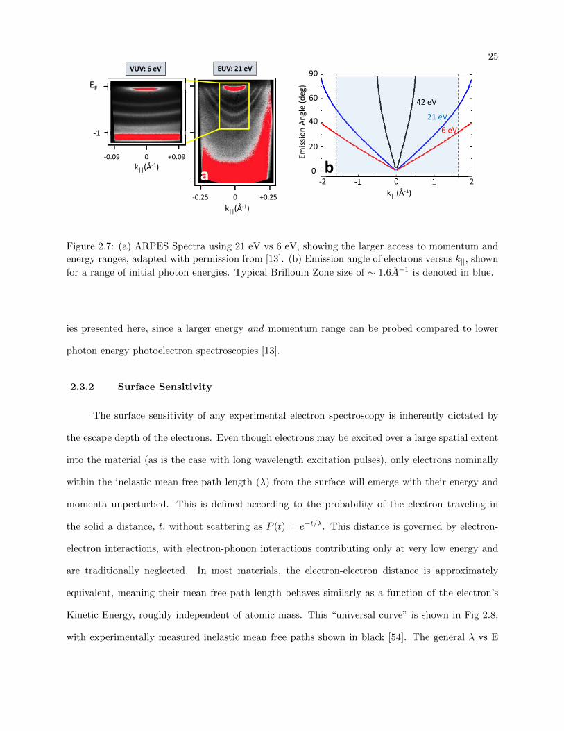
25EUV: 21 eVVUV: 6 eV
EF
‐1
‐0.09 +0.090k||(Å‐1)
‐0.25 +0.250k||(Å‐1)
a 0 1 2‐2 ‐10
20
40
60
90
6 eV21 eV
42 eV
k||(Å‐1)
Emission An
gle (deg)
b
Figure 2.7: (a) ARPES Spectra using 21 eV vs 6 eV, showing the larger access to momentum andenergy ranges, adapted with permission from [13]. (b) Emission angle of electrons versus k||, shown
for a range of initial photon energies. Typical Brillouin Zone size of ∼ 1.6A−1 is denoted in blue.
ies presented here, since a larger energy and momentum range can be probed compared to lower
photon energy photoelectron spectroscopies [13].
2.3.2 Surface Sensitivity
The surface sensitivity of any experimental electron spectroscopy is inherently dictated by
the escape depth of the electrons. Even though electrons may be excited over a large spatial extent
into the material (as is the case with long wavelength excitation pulses), only electrons nominally
within the inelastic mean free path length (λ) from the surface will emerge with their energy and
momenta unperturbed. This is defined according to the probability of the electron traveling in
the solid a distance, t, without scattering as P (t) = e−t/λ. This distance is governed by electron-
electron interactions, with electron-phonon interactions contributing only at very low energy and
are traditionally neglected. In most materials, the electron-electron distance is approximately
equivalent, meaning their mean free path length behaves similarly as a function of the electron’s
Kinetic Energy, roughly independent of atomic mass. This “universal curve” is shown in Fig 2.8,
with experimentally measured inelastic mean free paths shown in black [54]. The general λ vs E
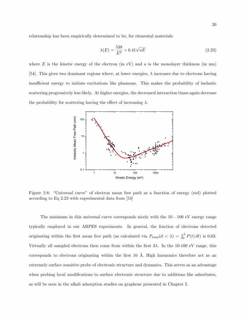
26
relationship has been empirically determined to be, for elemental materials:
λ(E) =538
E2+ 0.41
√aE (2.23)
where E is the kinetic energy of the electron (in eV) and a is the monolayer thickness (in nm)
[54]. This gives two dominant regions where, at lower energies, λ increases due to electrons having
insufficient energy to initiate excitations like plasmons. This makes the probability of inelastic
scattering progressively less likely. At higher energies, the decreased interaction times again decrease
the probability for scattering having the effect of increasing λ.
1 10 100 10000.1
1
10
100
Inel
astic
Mea
n Fr
ee P
ath
(nm
)
Kinetic Energy (eV)
Figure 2.8: “Universal curve” of electron mean free path as a function of energy (red) plottedaccording to Eq 2.23 with experimental data from [54]
The minimum in this universal curve corresponds nicely with the 10 - 100 eV energy range
typically employed in our ARPES experiments. In general, the fraction of electrons detected
originating within the first mean free path (as calculated via Ptotal(d < λ) =∫ λ
0 P (t) dt) is 0.63.
Virtually all sampled electrons then come from within the first 3λ. In the 10-100 eV range, this
corresponds to electrons originating within the first 10 A. High harmonics therefore act as an
extremely surface sensitive probe of electronic structure and dynamics. This serves as an advantage
when probing local modifications to surface electronic structure due to additions like adsorbates,
as will be seen in the alkali adsorption studies on graphene presented in Chapter 5.
27
By the same token, one consequence of this surface sensitivity is the possibility for a dominant
contribution to the photoemission spectra from surface contamination or scattering due to surface
roughness. This necessitates using well-ordered, atomically clean surfaces that require preparation
in-situ in the Ultra High Vacuum environment.
2.3.3 Background Separation
Inherent to any photoemission process is a low-energy secondary electron background. In
photoemitting a given material’s density of states, shown in gray in Fig 2.9 (left), a low energy
background is formed (brown) from photoexcited electrons scattering inelastically within the crystal
prior to escaping the surface. For the IR pump and EUV/VUV probe used here, each source
contributes to this background. In the directly photoemitted electrons using EUV/VUV photons
(right, top), a large secondary electron background can be seen below ∼6 eV. This background is
directly dependent on the surface/ crystal quality, with increased defects and impurities increasing
the number of scattering centers for the photoexcited electrons and yielding a higher number of
secondary electrons. With only IR light incident, the photon energy being below the work function
of the material means that absorption of multiple photons is necessary to photoemit an electron
from the surface. In the case shown in Fig 2.9 (right, bottom), this Above Threshold Photoemission
(ATP) has a significant contribution up to 20 eV kinetic energy when initiated with 1.5 eV IR
light. Shown for the typical intensities employed in the experiments here, these intensities (∼ 1011
W/cm2) are necessary to create the large hot electron populations studied in Chapter 5 and a
sufficient dressing field for the interferometric measurements in Chapter 4. This ATP background
is lessened, but still present up to ∼ 7 eV, when using longer dressing wavelength light (0.95 eV at
1010 W/cm2) due to the increased number of photons necessary to photoemit electrons from the
surface.
Combined, these effects are seen to produce a dominant low-energy background that can
bury the spectroscopic features one is interested in probing. On surfaces compared to atomic
photoemission, increased ATP is seen from local field enhancement and distortion effects around
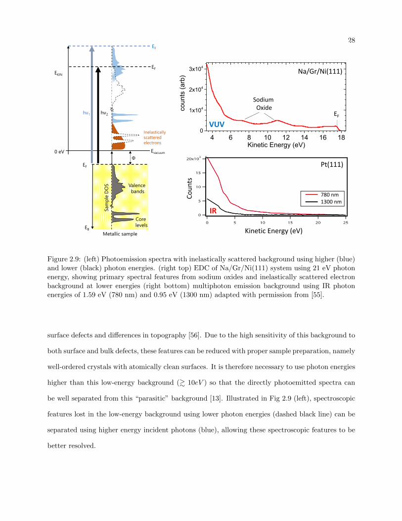
28
4 6 8 10 12 14 16 180
1x10⁴
2x10⁴
3x10⁴
coun
ts (a
rb)
Kinetic Energy (eV)
Valence bands
Sam
ple
DOS
Metallic sample
EF
Evacuum
EKIN
hν1
EB
Φ
Inelasticallyscattered electrons
Core levels
0 eV
EF
EF
hν2
Na/Gr/Ni(111)
780 nm1300 nm
Pt(111)
VUV
IR
Sodium Oxide
EF
Kinetic Energy (eV)
Coun
ts
Figure 2.9: (left) Photoemission spectra with inelastically scattered background using higher (blue)and lower (black) photon energies. (right top) EDC of Na/Gr/Ni(111) system using 21 eV photonenergy, showing primary spectral features from sodium oxides and inelastically scattered electronbackground at lower energies (right bottom) multiphoton emission background using IR photonenergies of 1.59 eV (780 nm) and 0.95 eV (1300 nm) adapted with permission from [55].
surface defects and differences in topography [56]. Due to the high sensitivity of this background to
both surface and bulk defects, these features can be reduced with proper sample preparation, namely
well-ordered crystals with atomically clean surfaces. It is therefore necessary to use photon energies
higher than this low-energy background (& 10eV ) so that the directly photoemitted spectra can
be well separated from this “parasitic” background [13]. Illustrated in Fig 2.9 (left), spectroscopic
features lost in the low-energy background using lower photon energies (dashed black line) can be
separated using higher energy incident photons (blue), allowing these spectroscopic features to be
better resolved.
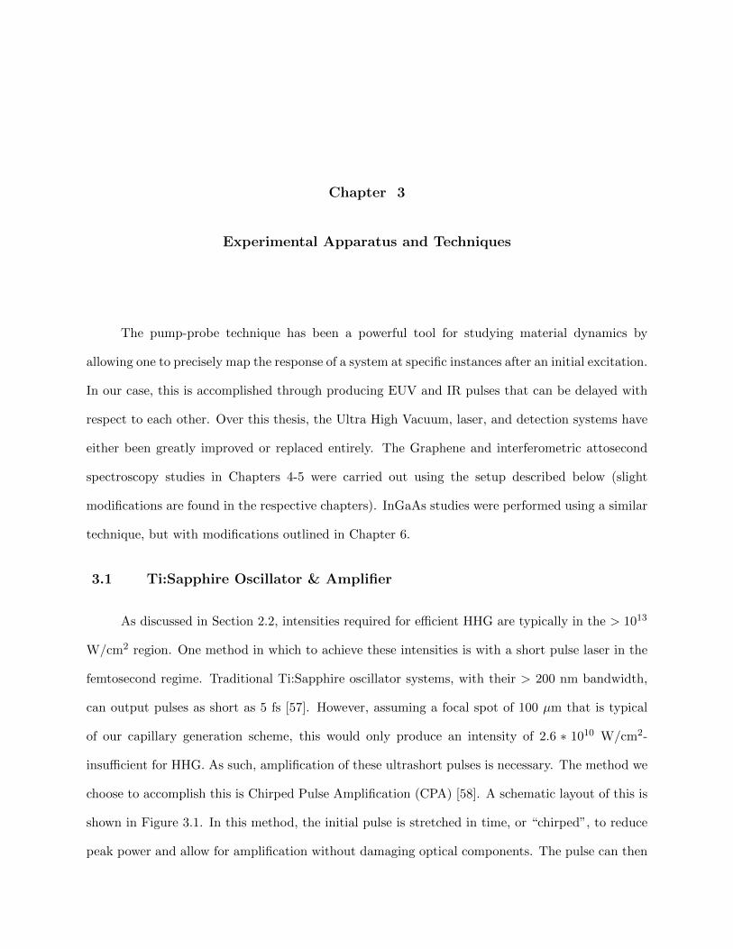
Chapter 3
Experimental Apparatus and Techniques
The pump-probe technique has been a powerful tool for studying material dynamics by
allowing one to precisely map the response of a system at specific instances after an initial excitation.
In our case, this is accomplished through producing EUV and IR pulses that can be delayed with
respect to each other. Over this thesis, the Ultra High Vacuum, laser, and detection systems have
either been greatly improved or replaced entirely. The Graphene and interferometric attosecond
spectroscopy studies in Chapters 4-5 were carried out using the setup described below (slight
modifications are found in the respective chapters). InGaAs studies were performed using a similar
technique, but with modifications outlined in Chapter 6.
3.1 Ti:Sapphire Oscillator & Amplifier
As discussed in Section 2.2, intensities required for efficient HHG are typically in the > 1013
W/cm2 region. One method in which to achieve these intensities is with a short pulse laser in the
femtosecond regime. Traditional Ti:Sapphire oscillator systems, with their > 200 nm bandwidth,
can output pulses as short as 5 fs [57]. However, assuming a focal spot of 100 µm that is typical
of our capillary generation scheme, this would only produce an intensity of 2.6 ∗ 1010 W/cm2-
insufficient for HHG. As such, amplification of these ultrashort pulses is necessary. The method we
choose to accomplish this is Chirped Pulse Amplification (CPA) [58]. A schematic layout of this is
shown in Figure 3.1. In this method, the initial pulse is stretched in time, or “chirped”, to reduce
peak power and allow for amplification without damaging optical components. The pulse can then
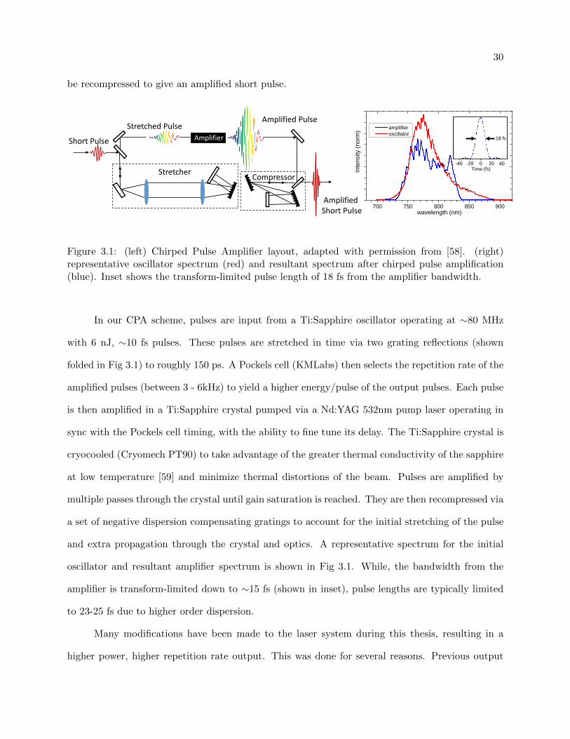
30
be recompressed to give an amplified short pulse.
700 750 800 850 900
Inte
nsity
(nor
m)
wavelength (nm)
amplifier oscillator
20 40-20-40 0Time (fs)
18 fs
Stretcher Compressor
Stretched Pulse
Short Pulse
Amplified Pulse
Amplified Short Pulse
Amplifier
Figure 3.1: (left) Chirped Pulse Amplifier layout, adapted with permission from [58]. (right)representative oscillator spectrum (red) and resultant spectrum after chirped pulse amplification(blue). Inset shows the transform-limited pulse length of 18 fs from the amplifier bandwidth.
In our CPA scheme, pulses are input from a Ti:Sapphire oscillator operating at ∼80 MHz
with 6 nJ, ∼10 fs pulses. These pulses are stretched in time via two grating reflections (shown
folded in Fig 3.1) to roughly 150 ps. A Pockels cell (KMLabs) then selects the repetition rate of the
amplified pulses (between 3 - 6kHz) to yield a higher energy/pulse of the output pulses. Each pulse
is then amplified in a Ti:Sapphire crystal pumped via a Nd:YAG 532nm pump laser operating in
sync with the Pockels cell timing, with the ability to fine tune its delay. The Ti:Sapphire crystal is
cryocooled (Cryomech PT90) to take advantage of the greater thermal conductivity of the sapphire
at low temperature [59] and minimize thermal distortions of the beam. Pulses are amplified by
multiple passes through the crystal until gain saturation is reached. They are then recompressed via
a set of negative dispersion compensating gratings to account for the initial stretching of the pulse
and extra propagation through the crystal and optics. A representative spectrum for the initial
oscillator and resultant amplifier spectrum is shown in Fig 3.1. While, the bandwidth from the
amplifier is transform-limited down to ∼15 fs (shown in inset), pulse lengths are typically limited
to 23-25 fs due to higher order dispersion.
Many modifications have been made to the laser system during this thesis, resulting in a
higher power, higher repetition rate output. This was done for several reasons. Previous output
31
powers were, at maximum, 2 mJ /pulse at 2 kHz with 25 fs pulses. High output powers (ie. high
energy/pulse) are desirable for efficient HHG of higher energy photons in gases like Helium (> 80
eV). In our pump/probe layout, it also provides sufficient power per branch for EUV generation as
well as low conversion efficiency processes like optical parametric amplification (OPA) for longer
pump wavelengths [55].
While maintaining a high energy per pulse, a higher repetition rate was also advantageous.
In addition to obviously generating a higher volume of detected events in real time, this offers some
advantages specific to our photoemission process. Specifically, maintaining the same number of
photoelectron events per second, less photoelectrons per pulse is preferred to give increased energy
resolution in the resultant spectra. This advantage can be understood when more closely analyzing
the nature of the photoemitted electron bunch from the surface. The number of photoelectrons
emitted from the surface is proportional to the number of incident EUV photons per pulse. Upon
being emitted from the surface with the ultrashort pulse, this results in a closely packed volume of
electrons that can Coulomb interact when in sufficiently high numbers. This Coulomb interaction
has been seen to give energy shifts, distortions in lineshape, and broadening of spectral features due
to the modifications to the electron’s kinetic energy on the way to the detector[60, 61]. An analytical
model of these space charge effects taking into account electron-electron Coulomb interactions,
neglecting effects like induced image charges at the surface, can be used to calculate the energy
broadening, ∆E, in a disk of photoemitted electrons of a radius, r0. This is calculated according
to:
∆E = [2e
πε0(
2
3π+
1
6)]1/2
√Ei(
N
r0)1/2 (3.1)
where Ei is the initial kinetic energy of the emitted electrons, N is the number of electrons in
the packet, e is the elementary charge, and ε0 is the vacuum permittivity [62]. This model, with
∆E ∝ N1/2, has been seen to agree with experimental data of electrons emitted via femtosecond
pulses quite well [60, 61]. It should be noted that this dependence is observed to be closer to a linear
relationship with N for picosecond pulses [63, 64] due to the larger lateral extent of the emitted
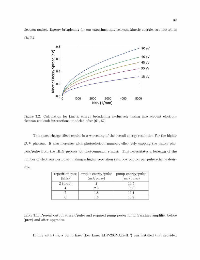
32
electron packet. Energy broadening for our experimentally relevant kinetic energies are plotted in
Fig 3.2.
0 1000 2000 3000 4000 50000.0
0.2
0.4
0.6
0.8
Kine
tic Ene
rgy Spread
(eV)
N/r0 (1/mm)
15 eV
30 eV
45 eV
60 eV
90 eV
Figure 3.2: Calculation for kinetic energy broadening exclusively taking into account electron-electron coulomb interactions, modeled after [61, 62].
This space charge effect results in a worsening of the overall energy resolution For the higher
EUV photons. It also increases with photoelectron number, effectively capping the usable pho-
tons/pulse from the HHG process for photoemission studies. This necessitates a lowering of the
number of electrons per pulse, making a higher repetition rate, low photon per pulse scheme desir-
able.
repetition rate output energy/pulse pump energy/pulse(kHz) (mJ/pulse) (mJ/pulse)
2 (prev) 2 19.5
4 2.3 18.6
5 1.8 16.1
6 1.6 13.2
Table 3.1: Present output energy/pulse and required pump power for Ti:Sapphire amplifier before(prev) and after upgrades.
In line with this, a pump laser (Lee Laser LDP-200MQG-HP) was installed that provided
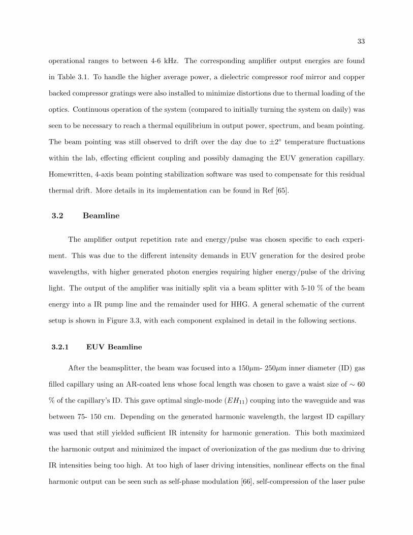
33
operational ranges to between 4-6 kHz. The corresponding amplifier output energies are found
in Table 3.1. To handle the higher average power, a dielectric compressor roof mirror and copper
backed compressor gratings were also installed to minimize distortions due to thermal loading of the
optics. Continuous operation of the system (compared to initially turning the system on daily) was
seen to be necessary to reach a thermal equilibrium in output power, spectrum, and beam pointing.
The beam pointing was still observed to drift over the day due to ±2 temperature fluctuations
within the lab, effecting efficient coupling and possibly damaging the EUV generation capillary.
Homewritten, 4-axis beam pointing stabilization software was used to compensate for this residual
thermal drift. More details in its implementation can be found in Ref [65].
3.2 Beamline
The amplifier output repetition rate and energy/pulse was chosen specific to each experi-
ment. This was due to the different intensity demands in EUV generation for the desired probe
wavelengths, with higher generated photon energies requiring higher energy/pulse of the driving
light. The output of the amplifier was initially split via a beam splitter with 5-10 % of the beam
energy into a IR pump line and the remainder used for HHG. A general schematic of the current
setup is shown in Figure 3.3, with each component explained in detail in the following sections.
3.2.1 EUV Beamline
After the beamsplitter, the beam was focused into a 150µm- 250µm inner diameter (ID) gas
filled capillary using an AR-coated lens whose focal length was chosen to gave a waist size of ∼ 60
% of the capillary’s ID. This gave optimal single-mode (EH11) couping into the waveguide and was
between 75- 150 cm. Depending on the generated harmonic wavelength, the largest ID capillary
was used that still yielded sufficient IR intensity for harmonic generation. This both maximized
the harmonic output and minimized the impact of overionization of the gas medium due to driving
IR intensities being too high. At too high of laser driving intensities, nonlinear effects on the final
harmonic output can be seen such as self-phase modulation [66], self-compression of the laser pulse
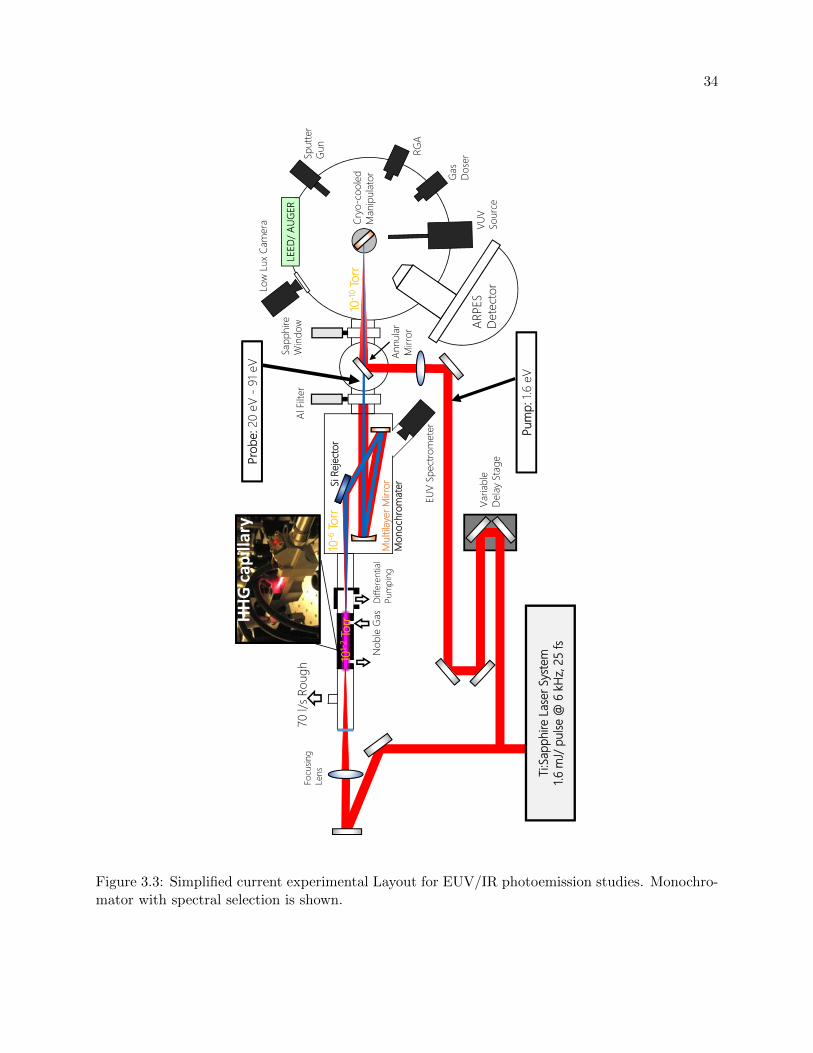
34
Ti:S
apph
ireLa
ser S
yste
m1.6
mJ/
pulse
@ 6
kHz
, 25
fs
70 l/
s Rou
gh
Nob
le G
as
Varia
ble
Delay
Sta
ge
Al F
ilter
Sapp
hire
W
indo
w
EUV
Spec
trom
eter
ARPE
S De
tect
orLow
Lux C
amer
aPr
obe:
20
eV -
91 e
V
Pum
p: 1.
6 eV
VUV
Sour
ce
Gas
Dose
r
Cryo
-coo
led
Man
ipul
ator
Mul
tilaye
r Mirr
or
Mon
ochr
omat
erSi R
ejec
tor
Annu
larM
irror
HHG cap
illary
Sput
ter
Gun
RGA
Diffe
rent
ial
Pum
ping
Focu
sing
Lens
10-1
0To
rr10
-6To
rr10
1-2
Torr
Figure 3.3: Simplified current experimental Layout for EUV/IR photoemission studies. Monochro-mator with spectral selection is shown.
35
during propagation [67], or spectral blue shifting [68]. The specifics of the generating parameters
for the range of harmonic wavelengths used in experiments discussed here are presented below.
3.2.1.1 High Harmonic Generation Schemes
Core level states of a material are accessible by using higher photon energies. However, the
added complication of variation in photoemission cross section of spectral features as a function of
photon wavelength mean that simply choosing the highest or brightest photon energy may be ill
suited for a specific material. For example, the surface state of Cu(111), studied in detail in Chapter
4, has multiple peaks in its relative intensity compared to neighboring states when incident photon
energy is scanned- occurring at photon energies of 6 eV [69] and 70 eV [70] and nearly vanishing at
“mid-range” energies ∼30 eV. With the additional desire to perform experiments requiring resonant
excitation, tunability of the high harmonic source over a large photon energy range is preferred in
order to offer the highest experimental capability possible.
Laser-driven harmonics have traditionally required a trade-off between energy resolution,
temporal resolution, and overall photon flux. The time-bandwidth limit necessarily dictates a
trade-off between pulse length and bandwidth of the harmonics, as modeled by:
∆E∆t = α ∗ 4.141 (3.2)
where E is the energy bandwidth in eV, t is the pulse length in fs, and α either 0.44 or 0.32 for
Gaussian or Sech2 pulses, respectively. For a 10 fs Gaussian harmonic pulse, the energy resolution
of the photoemitted electrons is already larger than 180 meV. In general, therefore, higher harmonic
photon energies are characterized by an increasingly broader energy bandwidth and lower photon
flux. This introduces another trade off of energy resolution for access to a greater range of electron
binding energies. This trend can be seen in the generation parameters for 4 common harmonics
used throughout this thesis (and in experimental attempts not included in this work), namely 22,
42, 65, and 90 eV. Characteristic generation parameters for these wavelengths such as gas medium,
typical optimal gas pressure, energy bandwidth, estimated photon flux, and corresponding spectral
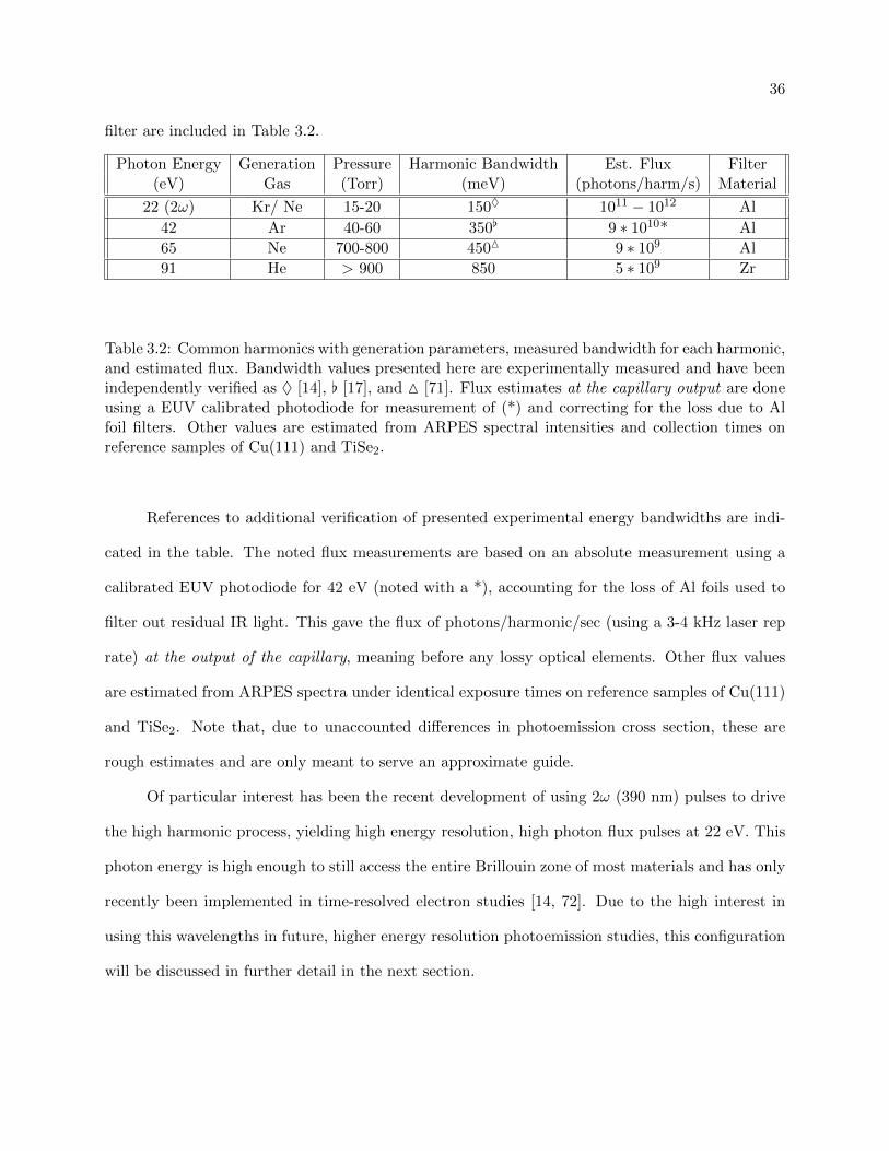
36
filter are included in Table 3.2.
Photon Energy Generation Pressure Harmonic Bandwidth Est. Flux Filter(eV) Gas (Torr) (meV) (photons/harm/s) Material
22 (2ω) Kr/ Ne 15-20 150♦ 1011 − 1012 Al
42 Ar 40-60 350[ 9 ∗ 1010* Al
65 Ne 700-800 450M 9 ∗ 109 Al
91 He > 900 850 5 ∗ 109 Zr
Table 3.2: Common harmonics with generation parameters, measured bandwidth for each harmonic,and estimated flux. Bandwidth values presented here are experimentally measured and have beenindependently verified as ♦ [14], [ [17], and M [71]. Flux estimates at the capillary output are doneusing a EUV calibrated photodiode for measurement of (*) and correcting for the loss due to Alfoil filters. Other values are estimated from ARPES spectral intensities and collection times onreference samples of Cu(111) and TiSe2.
References to additional verification of presented experimental energy bandwidths are indi-
cated in the table. The noted flux measurements are based on an absolute measurement using a
calibrated EUV photodiode for 42 eV (noted with a *), accounting for the loss of Al foils used to
filter out residual IR light. This gave the flux of photons/harmonic/sec (using a 3-4 kHz laser rep
rate) at the output of the capillary, meaning before any lossy optical elements. Other flux values
are estimated from ARPES spectra under identical exposure times on reference samples of Cu(111)
and TiSe2. Note that, due to unaccounted differences in photoemission cross section, these are
rough estimates and are only meant to serve an approximate guide.
Of particular interest has been the recent development of using 2ω (390 nm) pulses to drive
the high harmonic process, yielding high energy resolution, high photon flux pulses at 22 eV. This
photon energy is high enough to still access the entire Brillouin zone of most materials and has only
recently been implemented in time-resolved electron studies [14, 72]. Due to the high interest in
using this wavelengths in future, higher energy resolution photoemission studies, this configuration
will be discussed in further detail in the next section.
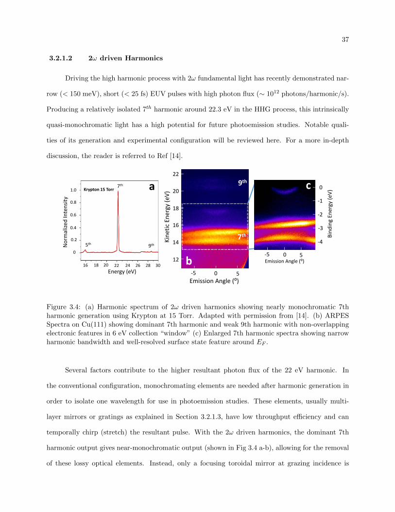
37
3.2.1.2 2ω driven Harmonics
Driving the high harmonic process with 2ω fundamental light has recently demonstrated nar-
row (< 150 meV), short (< 25 fs) EUV pulses with high photon flux (∼ 1012 photons/harmonic/s).
Producing a relatively isolated 7th harmonic around 22.3 eV in the HHG process, this intrinsically
quasi-monochromatic light has a high potential for future photoemission studies. Notable quali-
ties of its generation and experimental configuration will be reviewed here. For a more in-depth
discussion, the reader is referred to Ref [14].
22
20
18
16
14
12
‐5 0 5
Kine
tic Ene
rgy (eV)
Emission Angle (⁰)
1.0
0.8
0.6
0.4
0.2
0
16 18 20 22 24 26 28 30
5th 9th
7thKrypton 15 Torr
Energy (eV)
Normalize
d Intensity
7th
9th0
‐1
‐2
‐3
‐4
‐5 0 5
Bind
ing Energy (e
V)
Emission Angle (⁰)
a
b
c
Figure 3.4: (a) Harmonic spectrum of 2ω driven harmonics showing nearly monochromatic 7thharmonic generation using Krypton at 15 Torr. Adapted with permission from [14]. (b) ARPESSpectra on Cu(111) showing dominant 7th harmonic and weak 9th harmonic with non-overlappingelectronic features in 6 eV collection “window” (c) Enlarged 7th harmonic spectra showing narrowharmonic bandwidth and well-resolved surface state feature around EF .
Several factors contribute to the higher resultant photon flux of the 22 eV harmonic. In
the conventional configuration, monochromating elements are needed after harmonic generation in
order to isolate one wavelength for use in photoemission studies. These elements, usually multi-
layer mirrors or gratings as explained in Section 3.2.1.3, have low throughput efficiency and can
temporally chirp (stretch) the resultant pulse. With the 2ω driven harmonics, the dominant 7th
harmonic output gives near-monochromatic output (shown in Fig 3.4 a-b), allowing for the removal
of these lossy optical elements. Instead, only a focusing toroidal mirror at grazing incidence is
38
used to focus the harmonics onto the sample. Furthermore, in generating harmonics using 3.2 eV
driving light, resultant harmonics are produced with a spacing between harmonics of 6.4 eV. This
means that, when used in photoemission studies, replica spectra are produced every 6.4 eV Kinetic
Energy (shown in 3.4 b). This gives a 6.4 eV “window” in which to clearly capture the relevant
spectral features of the material without being overlapped with the adjacent harmonic. This is
sufficient for including the dominant valence structure of most materials.
Another advantage of the shorter wavelength driving laser is in the quantum efficiency of
the HHG process. A shorter driving wavelength means less spreading of the quantum electron
wavepacket upon ionization from the parent atom. This results in a higher recombination prob-
ability and an increase in the overall single-atom photon yield. Since single-atom HHG efficiency
scales with driving wavelength at λ−5 − λ−9, a doubling of the fundamental driving frequency
results in roughly two orders of magnitude increase in single-atom yield [48, 43, 12]. Due to the
electron spending less time in the continuum, this has the additional bonus of the electron motion,
and therefore harmonic bandwidth and central frequency, being less sensitive to the local plasma
conditions in the gas medium. The use of moderate intensities in the harmonic generation also
avoids the possible nonlinearities in the generating medium mentioned previously. This results in
a high yield, more stable harmonic source.
Understanding as to why the harmonic output results in such narrow energy bandwidth can
be seen when looking at the specifics of the harmonic generation. 2ω light is initially generated
using a 200 µm thick β barium borate (BBO) crystal in order to convert an incident beam of
1.8 mJ/pulse at 780nm into 390 nm centered light at 0.3 mJ/pulse (note: the spectra shown in
Fig 3.5 (right) used a 1.1 mJ/pulse 780nm beam with similar resultant power) and subsequently
focused into the gas medium. These pulses are not recompressed after these optical elements and
are estimated to be 35-40 fs long with ∼200 fs2 positive chirp). Due to the longer pulse length
of the generating light, while still maintaining sufficient intensities for HHG, the resultant energy
bandwidth is therefore narrower. This has been measured to yield 20 ± 16 fs harmonic pulses
[14] that are still sufficiently short for use in time-resolved studies. In photoemission studies, this
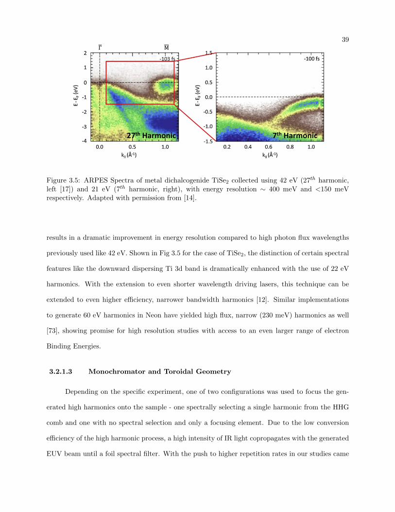
39
7th Harmonic27th Harmonic
Figure 3.5: ARPES Spectra of metal dichalcogenide TiSe2 collected using 42 eV (27th harmonic,left [17]) and 21 eV (7th harmonic, right), with energy resolution ∼ 400 meV and <150 meVrespectively. Adapted with permission from [14].
results in a dramatic improvement in energy resolution compared to high photon flux wavelengths
previously used like 42 eV. Shown in Fig 3.5 for the case of TiSe2, the distinction of certain spectral
features like the downward dispersing Ti 3d band is dramatically enhanced with the use of 22 eV
harmonics. With the extension to even shorter wavelength driving lasers, this technique can be
extended to even higher efficiency, narrower bandwidth harmonics [12]. Similar implementations
to generate 60 eV harmonics in Neon have yielded high flux, narrow (230 meV) harmonics as well
[73], showing promise for high resolution studies with access to an even larger range of electron
Binding Energies.
3.2.1.3 Monochromator and Toroidal Geometry
Depending on the specific experiment, one of two configurations was used to focus the gen-
erated high harmonics onto the sample - one spectrally selecting a single harmonic from the HHG
comb and one with no spectral selection and only a focusing element. Due to the low conversion
efficiency of the high harmonic process, a high intensity of IR light copropagates with the generated
EUV beam until a foil spectral filter. With the push to higher repetition rates in our studies came
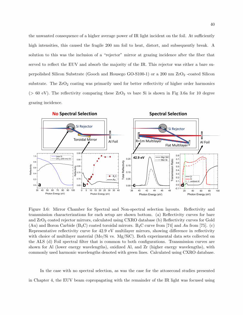
40
the unwanted consequence of a higher average power of IR light incident on the foil. At sufficiently
high intensities, this caused the fragile 200 nm foil to heat, distort, and subsequently break. A
solution to this was the inclusion of a “rejector” mirror at grazing incidence after the fiber that
served to reflect the EUV and absorb the majority of the IR. This rejector was either a bare su-
perpolished Silicon Substrate (Gooch and Housego GO-S100-1) or a 200 nm ZrO2 -coated Silicon
substrate. The ZrO2 coating was primarily used for better reflectivity of higher order harmonics
(> 60 eV). The reflectivity comparing these ZrO2 vs bare Si is shown in Fig 3.6a for 10 degree
grazing incidence.
38 40 42 44 46 48
0.00
0.05
0.10
0.15
0.20
Tota
l Ref
lect
ivity
Photon Energy (eV)
Mg/ SiC Mo/ Si
42.9 eV
Si RejectorSi Rejector
Flat Multilayer
No Spectral Selection
a
Al Foil
20 40 60 80 100-0.10.00.10.20.30.40.50.60.70.8
Tran
smis
sion
Rat
io
Photon Energy (eV)
Zr Al oxidized Al
R=1m MultilayerToroidal Mirror
30 40 50 60 70 80 90 100
0.0
0.2
0.4
0.6
0.8
1.0
Ref
lect
ivity
Photon Energy (eV)
bare Si ZrO2 (200 nm)/ Si
0 5 10 15 20 25 30 35 40
0.65
0.70
0.75
0.80
0.85
0.90
Ref
lect
ivity
Photon Energy (eV)
B4C Au
Al Foil
Spectral Selection
b c d
Figure 3.6: Mirror Chamber for Spectral and Non-spectral selection layouts. Reflectivity andtransmission characterizations for each setup are shown bottom. (a) Reflectivity curves for bareand ZrO2 coated rejector mirrors, calculated using CXRO database (b) Reflectivity curves for Gold(Au) and Boron Carbide (B4C) coated toroidal mirrors. B4C curve from [74] and Au from [75]. (c)Representative reflectivity curve for 42.9 eV multilayer mirrors, showing difference in reflectivitywith choice of multilayer material (Mo/Si vs. Mg/SiC). Both experimental data sets collected onthe ALS (d) Foil spectral filter that is common to both configurations. Transmission curves areshown for Al (lower energy wavelengths), oxidized Al, and Zr (higher energy wavelengths), withcommonly used harmonic wavelengths denoted with green lines. Calculated using CXRO database.
In the case with no spectral selection, as was the case for the attosecond studies presented
in Chapter 4, the EUV beam copropagating with the remainder of the IR light was focused using
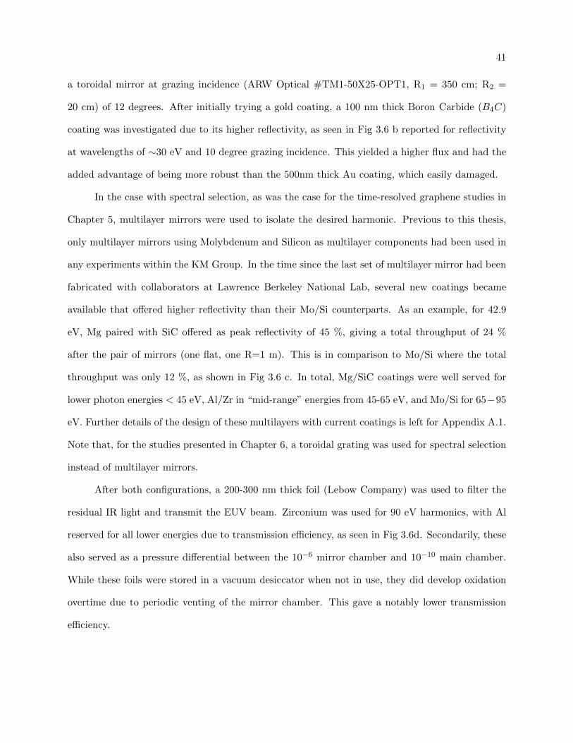
41
a toroidal mirror at grazing incidence (ARW Optical #TM1-50X25-OPT1, R1 = 350 cm; R2 =
20 cm) of 12 degrees. After initially trying a gold coating, a 100 nm thick Boron Carbide (B4C)
coating was investigated due to its higher reflectivity, as seen in Fig 3.6 b reported for reflectivity
at wavelengths of ∼30 eV and 10 degree grazing incidence. This yielded a higher flux and had the
added advantage of being more robust than the 500nm thick Au coating, which easily damaged.
In the case with spectral selection, as was the case for the time-resolved graphene studies in
Chapter 5, multilayer mirrors were used to isolate the desired harmonic. Previous to this thesis,
only multilayer mirrors using Molybdenum and Silicon as multilayer components had been used in
any experiments within the KM Group. In the time since the last set of multilayer mirror had been
fabricated with collaborators at Lawrence Berkeley National Lab, several new coatings became
available that offered higher reflectivity than their Mo/Si counterparts. As an example, for 42.9
eV, Mg paired with SiC offered as peak reflectivity of 45 %, giving a total throughput of 24 %
after the pair of mirrors (one flat, one R=1 m). This is in comparison to Mo/Si where the total
throughput was only 12 %, as shown in Fig 3.6 c. In total, Mg/SiC coatings were well served for
lower photon energies < 45 eV, Al/Zr in “mid-range” energies from 45-65 eV, and Mo/Si for 65−95
eV. Further details of the design of these multilayers with current coatings is left for Appendix A.1.
Note that, for the studies presented in Chapter 6, a toroidal grating was used for spectral selection
instead of multilayer mirrors.
After both configurations, a 200-300 nm thick foil (Lebow Company) was used to filter the
residual IR light and transmit the EUV beam. Zirconium was used for 90 eV harmonics, with Al
reserved for all lower energies due to transmission efficiency, as seen in Fig 3.6d. Secondarily, these
also served as a pressure differential between the 10−6 mirror chamber and 10−10 main chamber.
While these foils were stored in a vacuum desiccator when not in use, they did develop oxidation
overtime due to periodic venting of the mirror chamber. This gave a notably lower transmission
efficiency.
42
3.2.2 IR Beamline
The 5-10 % of the initial amplifier output was used as the pump/ dressing light for experiments
discussed here. The beam was then propagated using silver mirrors to minimize extra dispersion
that would increase pulse length. A computer interfaced delay stage (Aerotech ANT130-1110-
L-25DU-MP) was used to control the relative pump/ probe delay with a resolution of 200 as.
The beam was then focused using a R=3m concave silver mirror and entered into a high vacuum
“recombination chamber”, for copropogating the IR and EUV light. A silver 45 angled annular
mirror with a 1 mm hole through the center is used to reflect the outer 60 % of the IR light onto
the sample, while letting the EUV light propagate through the center hole. In this configuration,
the IR and EUV beams are collinear with < 0.1 between them, as verified through their optical
interference pattern projected onto a screen after propagation through the UHV chamber.
3.2.3 IR Pump Temporal Compression
Temporal compression of IR pulses has been previously done with Ti:Sapphire pulses from
30 fs down to < 5 fs [76]. This was primarily done with the aim of subsequently generating isolated
attoseconds bursts through high harmonic generation. However, in modern IR pump- EUV probe
schemes, the temporal resolution of the studied electron dynamics is limited due to the convolution
of the temporal width of the IR pulse with the EUV temporal pulse width. For the realm of surface
science, it is then already advantageous to temporally compress the IR pump pulse, therefore
increasing the overall temporal resolution of the studied dynamics. One implementation of this,
investigated during this thesis, is “self-phase modulation” (SPM), where the 30 fs pulse from the
Ti:Sapphire amplifier is compressed to achieve a < 10 fs pulse length. As the ultrashort pulse
propagates through a medium with an intensity dependent refractive index, a frequency shift is
induced in the spectral components in the pulse. For a positive nonlinear index gas according to:
n(I) = n0 + n2 ∗ I, where I is the laser intensity, n0 is the linear refractive index, and n2 is the
nonlinear refractive index (2nd order), this results in a broadening of the overall initial spectrum.
43
This greatly decreases the achievable driving pulse length according to the time-bandwidth limit.
The resultant positive dispersion of the pulse can then be compensated for with negative dispersion
compensating mirrors (chirped mirrors).
0 500 1000 1500 20000.0
0.5
1.0
1.5
2.0
2.5
3.0
pressure Torr
fiberlength
m
ArgonKryptonXenon
Figure 3.7: Calculation for optimal SPM length for a given pressure, calculated after [76]
In practice, this was achieved through focusing a 25 fs, 0.6 mJ/pulse into a hollow-core
gas-filled capillary. Fiber lengths of 20 cm and 1 m were investigated to determine the effects on
overall spectral broadening and throughput. Xenon, Krypton, and Argon gases were investigated
to determine the optimal gas for maximum spectral broadening and recompression. Estimates of
the optimal pressure for given fiber lengths were initially calculated according to literature [76]
using:
Loptimal ≈ (6LNLLD)1/2 (3.3)
where LNL is the nonlinear length calculated according to 1/γP0 where P0 is the peak power
of the pulse and γ is the nonlinear coefficient. γ can be calculated according to n2 ∗w0/cAeff where
w0 is the frequency of the driving laser, c is the speed of light, and Aeff is the area of the mode
coupled into the fiber. The dispersion length, LD, can be calculated according to T 20 /β2 where T0 is
the FWHM pulse length of the driving laser and β2 is the group velocity dispersion of the gas filled
fiber. Results of this calculation for a 200 µm waveguide are shown in Figure 3.7 using values of
44
n2 and β from literature [77, 78]. This gave rough estimates for expected optimal pressure ranges
for the 20 cm and 1 m fibers investigated.
Figure 3.8: SPM layout and pulse recompression using chirped mirrors and glass. FROG tracespre-SPM (25 fs) and post-compression (12 fs) are shown to the right using Krypon at 880 Torr.
The apparatus, shown in Figure 3.8, consisted of a 20 cm or 1 m, 400 µm ID gas-filled
capillary settled in a v-groove with horizontal and vertical translation stages mounted on the front
and back for alignment. To minimize defocusing of the input pulse due to the dominant higher-order
effects within the gas [79], gas was input at the exit of the capillary and evacuated at the entrance,
setting up a pressure gradient from 0 Torr to the nominally read value [80]. The output was then
recollimated and sent to a set of chirped mirrors for negative dispersion compensation (Layertec,
−40fs2 per reflection). Due to the set negative dispersion per reflection from the chirped mirrors,
finer adjustment to the dispersion compensation was done by over-compensating the dispersion
with the chirped mirrors (for a net negative dispersion), and adding glass to yield little to no
second order dispersion. Glass wedges were also inserted, mounted on horizontal translation stages
for fine tuning of this dispersion compensation. Pulse lengths were then verified using Frequency
Resolved Optical Gating (FROG) with an appropriately thin BBO (thickness = 100 µ m ) to phase
match the full bandwidth of the pulse. FROG traces yielding reconstructed pulse widths of 25 fs
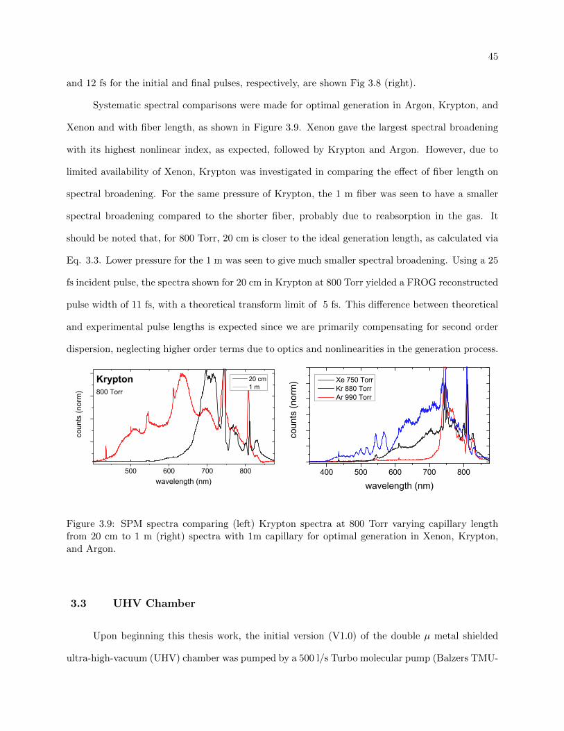
45
and 12 fs for the initial and final pulses, respectively, are shown Fig 3.8 (right).
Systematic spectral comparisons were made for optimal generation in Argon, Krypton, and
Xenon and with fiber length, as shown in Figure 3.9. Xenon gave the largest spectral broadening
with its highest nonlinear index, as expected, followed by Krypton and Argon. However, due to
limited availability of Xenon, Krypton was investigated in comparing the effect of fiber length on
spectral broadening. For the same pressure of Krypton, the 1 m fiber was seen to have a smaller
spectral broadening compared to the shorter fiber, probably due to reabsorption in the gas. It
should be noted that, for 800 Torr, 20 cm is closer to the ideal generation length, as calculated via
Eq. 3.3. Lower pressure for the 1 m was seen to give much smaller spectral broadening. Using a 25
fs incident pulse, the spectra shown for 20 cm in Krypton at 800 Torr yielded a FROG reconstructed
pulse width of 11 fs, with a theoretical transform limit of 5 fs. This difference between theoretical
and experimental pulse lengths is expected since we are primarily compensating for second order
dispersion, neglecting higher order terms due to optics and nonlinearities in the generation process.
500 600 700 800
coun
ts (n
orm
)
wavelength (nm)
20 cm 1 m
Krypton800 Torr
400 500 600 700 800
coun
ts (n
orm
)
wavelength (nm)
Xe 750 Torr Kr 880 Torr Ar 990 Torr
Figure 3.9: SPM spectra comparing (left) Krypton spectra at 800 Torr varying capillary lengthfrom 20 cm to 1 m (right) spectra with 1m capillary for optimal generation in Xenon, Krypton,and Argon.
3.3 UHV Chamber
Upon beginning this thesis work, the initial version (V1.0) of the double µ metal shielded
ultra-high-vacuum (UHV) chamber was pumped by a 500 l/s Turbo molecular pump (Balzers TMU-
46
520-SG) and a 270 l/s ion pump (Varian VacIon Plus). The µ metal shielding was used to prevent
residual magnetic fields from penetrating into the chamber and altering the electron trajectory into
the analyzer. The current chamber (V2.0), is fabricated directly from µ metal and pumped by
the 270 l/s ion pump and a 700 l/s magnetically-levitated turbo pump (Pfieffer Hi Pac 700 M)
to reduce vibrations. In addition to being able to accommodate the angle-resolved detector, the
dramatically increased number of vacuum ports in the new chamber design gave more versatility
in experimental design and positioning new components. Base pressures were 2 ∗ 10−10 Torr and
maximally 8 ∗ 10−10 Torr during pump/probe measurements due to small pinholes in the pressure
differential Al filter.
3.3.1 Sample Preparation Tools
Several tools are available in the UHV chamber to aid in preparation of atomically ordered and
clean surfaces for photoemission measurements. An Ar-ion sputter gun (LK Technologies NGI3000-
SE) was used to remove the top monolayers of atoms in metal samples (primarily Cu(111) in the
studies presented here) via collisionally ejecting surface atoms through bombardment with energetic
Ar ions. Reconstructing the surface ordering was then achieved through thermal annealing.
A gas doser with a precision leak valve was used for creating a locally concentrated source for
surface deposition. This was used in deposition of oxygen, noble gases, as well as the ethylene gas
for use in in situ graphene growth. The locally high pressure environment near the sample during
dosing enabled having a lower overall chamber pressure, minimizing pump-down time back to the
10−10 Torr background and residual chamber contamination.
An alkali metal doser (SAES Getter source) equipped with 2 filaments was mounted on a
long-travel linear shift attached to the main chamber through a pneumatic value and differentially
pumped through a 80 l/s turbo pump (Pfeiffer HiCube 80 Eco). This enabled adjustable and close
positioning of the alkali filaments to the sample during dosing. It also allowed for changing of
the filaments without the need for breaking main chamber vacuum by withdrawing the filaments
and closing the pneumatic valve. The filament attachment could then be independently baked
47
and reopened to the main chamber with minimal contamination. Filaments were well outgassed
after insertion through slowly ramping an applied current (using a GWInstek GPP-1810HP) from
0-5A while monitoring outgassed compounds using the Residual Gas Analyzer (RGA, as discussed
below). During dosing, possible contaminants were also monitored using the RGA.
3.3.2 Sample Characterization Tools
Extensive characterization of the sample surface was done prior to all EUV measurements to
ensure a well defined and understood surface before adding in the experimental difficulties of EUV
generation and pump/probe photoemission. A Low Energy Electron Diffraction (LEED) spectrom-
eter (OCI BDL800IR) was used to determine crystal orientations via imaging the diffraction of low
energy electrons from the sample surface onto a phosphor screen. This served to determine sample
orientation as well as the atomic ordering of the surface and was routinely used to diagnose the
degree of surface contamination on metallic samples and surface quality of graphene samples. In
the case of rotated crystalline overlayers, arcs in the diffraction pattern were observed, as was the
case on multilayer C-terminated Graphene/SiC. Poor crystalline quality was seen to give blurred
diffraction spots.
The implementation of a incoherent source of EUV light was also crucial for efficient sur-
face characterization. Due to the typically broad bandwidth and lower flux of EUV harmonics, a
high-intensity, narrow bandwidth EUV source was preferred to give high-resolution, quick charac-
terization of prepared surfaces. These characterizations were indispensable in providing feedback
during the “learning phases” of determining the proper surface cleaning and sample dosing proce-
dures, without the additional difficulty of optimizing the EUV generation setup. A duo plasmatron
discharge lamp [81] (Spec UVS 300) was used for this purpose. Electrons are initially generated
via a tungsten filament in an ambient 10−4 Torr He environment and accelerated towards a posi-
tivity biased “funnel shaped” aperture. A strongly bottlenecked magnetic field confines electrons
generated from electron/gas collisions into a narrow region between this cathode and anode. The
resultant EUV emission from the plasma is then leaked through the aperture and, in our case,
48
focused to a ∼ 1 mm spot after a metal capillary. Ratios between the two dominant emission lines
could be tuned to give either primarily He I (21.2 eV) or He II (40.8 eV) radiation with a flux of
1016 photons/sr·s.
Lastly, a Residual Gas Analyzer (RGA, Leybold Inficon Transpector 2) was used to monitor
the partial pressure of gaseous species in the chamber. This mass spectrometer was used to primarily
detect atmospheric and hydrocarbon contaminants in the system upon alkali and gaseous dosing.
Using the RGA, Temperature Programmable Desorption (TPD) studies could also be performed
by ramping the sample temperature at a fixed rate and observing the desorbed species from the
sample surface. This could then be used to inform on the nature of the chemical bonding of the
adsorbed species on the surface.
3.4 ARPES Detector
The most beneficial upgrade to the system implemented during this thesis has been the
installation of an angle-resolved electron detector (Specs Phoibos 100). Previous experiments were
carried out using a time-of-flight detector with a narrow photoemitted electron acceptance angle,
as described in [82]. This collected an energy density curve (EDC) for effectively one photoemitted
electron angle relative to the surface. In order to obtain similar spectral information to angle-
resolved detectors, multiple EDCs needed to be collected for different photoemitted angles (via
rotating the sample angle relative to the detector) and the spectra subsequently “stitched” together
to form a full band map as a function of θ. This time-consuming scheme is not feasible for time-
resolved measurements where long integration times would mean full scans would require days of
integration stability. Hemispherical angle-resolved detectors, therefore, have become the dominant
design for obtaining high energy and angular resolution spectra of photoemitted electrons. The
detector is composed of primary three sections: An electrostatic lens system for collecting and
separating electrons by their photoemitted angle, a hemispherical analyzer for separating electrons
based on their kinetic energy, and a detector for electron multiplication and actually imaging the
2D electron distribution. The following sections will individually discuss the implementation of
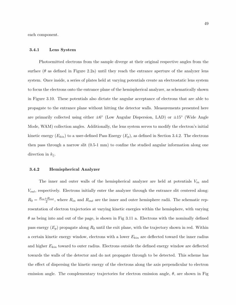
49
each component.
3.4.1 Lens System
Photoemitted electrons from the sample diverge at their original respective angles from the
surface (θ as defined in Figure 2.2a) until they reach the entrance aperture of the analyzer lens
system. Once inside, a series of plates held at varying potentials create an electrostatic lens system
to focus the electrons onto the entrance plane of the hemispherical analyzer, as schematically shown
in Figure 3.10. These potentials also dictate the angular acceptance of electrons that are able to
propagate to the entrance plane without hitting the detector walls. Measurements presented here
are primarily collected using either ±6 (Low Angular Dispersion, LAD) or ±15 (Wide Angle
Mode, WAM) collection angles. Additionally, the lens system serves to modify the electron’s initial
kinetic energy (Ekin) to a user-defined Pass Energy (Ep), as defined in Section 3.4.2. The electrons
then pass through a narrow slit (0.5-1 mm) to confine the studied angular information along one
direction in k||.
3.4.2 Hemispherical Analyzer
The inner and outer walls of the hemispherical analyzer are held at potentials Vin and
Vout, respectively. Electrons initially enter the analyzer through the entrance slit centered along:
R0 = Rin+Rout2 , where Rin and Rout are the inner and outer hemisphere radii. The schematic rep-
resentation of electron trajectories at varying kinetic energies within the hemisphere, with varying
θ as being into and out of the page, is shown in Fig 3.11 a. Electrons with the nominally defined
pass energy (Ep) propagate along R0 until the exit plane, with the trajectory shown in red. Within
a certain kinetic energy window, electrons with a lower Ekin are deflected toward the inner radius
and higher Ekin toward to outer radius. Electrons outside the defined energy window are deflected
towards the walls of the detector and do not propagate through to be detected. This scheme has
the effect of dispersing the kinetic energy of the electrons along the axis perpendicular to electron
emission angle. The complementary trajectories for electron emission angle, θ, are shown in Fig
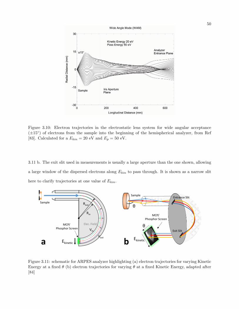
50
Figure 3.10: Electron trajectories in the electrostatic lens system for wide angular acceptance(±15) of electrons from the sample into the beginning of the hemispherical analyzer, from Ref[83]. Calculated for a Ekin = 20 eV and Ep = 50 eV.
3.11 b. The exit slit used in measurements is usually a large aperture than the one shown, allowing
a large window of the dispersed electrons along Ekin to pass through. It is shown as a narrow slit
here to clarify trajectories at one value of Ekin.
Ekinetic
Rin
Rout
MCP/ Phosphor Screen
Elec. Field
Vin
Vout
Sample
a
θ
Ekinetic
Sample
b
Entrance Slit
Exit Slit
MCP/ Phosphor Screen
θ
Figure 3.11: schematic for ARPES analyzer highlighting (a) electron trajectories for varying KineticEnergy at a fixed θ (b) electron trajectories for varying θ at a fixed Kinetic Energy, adapted after[84]
51
3.4.3 Electron Detection
The 2D electron pattern, being dispersed according to θ in one direction and Ekin in the other,
is then amplified via a set of multichannel plates (MCP). The secondary electron cascade, usually a
multiplication of 107 per incident electron, can then detected after the MCP by a phosphor screen,
registering each electron-cascade packet as a glowing point on the screen. A charge-couple-device
(CCD) camera is then used to image the phosphor screen. Analysis software is then used to assign
energy and angle values to the 1376 x 1040 channels. It should be noted that, due to aberrations
in the lens system, significant “warping” occurs for the lower kinetic energy region of the recorded
spectra. The degree of this spectral warping as a function of angle and energy can be calculated
and is corrected for in presented spectra. Additionally, the photoemission angle is converted to k||,
according to Equation 2.8.
3.5 Custom Cryogenic Cooling Manipulator and Sample Holder
One of the largest engineering and design endeavors during this thesis was the optimization
of a sample holder design that had:
(1) high temperature capabilities, for metal sample surface preparation and in-situ graphene
growth
(2) low temperature capabilities, for surface-adsorbate systems (metal/CO, metal/alkali, metal/noble
gas) and low temperature phase-change materials (e.g. metal di-chalcogenides)
The initial sample holder design (V1.0) had been used to primarily investigate single-crystal
metal surfaces. Mounted on a 4-axis manipulator (horizontal and vertical translation with rotation
about the vertical axis), the sample was permanently mounted in the proper orientation. Heating
was controlled through directly flowing a high current (> 10A) through the crystal, with cooling
achieved through contacted copper feedthrough connections coupled to an external liquid nitrogen
reservoir. Temperature performance data for this and subsequent designs can be found in Table
3.3.
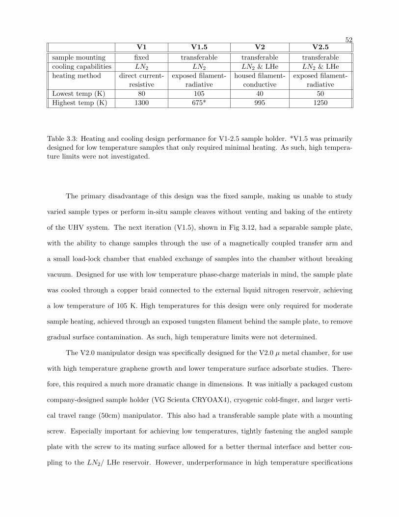
52V1 V1.5 V2 V2.5
sample mounting fixed transferable transferable transferable
cooling capabilities LN2 LN2 LN2 & LHe LN2 & LHe
heating method direct current- exposed filament- housed filament- exposed filament-resistive radiative conductive radiative
Lowest temp (K) 80 105 40 50
Highest temp (K) 1300 675* 995 1250
Table 3.3: Heating and cooling design performance for V1-2.5 sample holder. *V1.5 was primarilydesigned for low temperature samples that only required minimal heating. As such, high tempera-ture limits were not investigated.
The primary disadvantage of this design was the fixed sample, making us unable to study
varied sample types or perform in-situ sample cleaves without venting and baking of the entirety
of the UHV system. The next iteration (V1.5), shown in Fig 3.12, had a separable sample plate,
with the ability to change samples through the use of a magnetically coupled transfer arm and
a small load-lock chamber that enabled exchange of samples into the chamber without breaking
vacuum. Designed for use with low temperature phase-charge materials in mind, the sample plate
was cooled through a copper braid connected to the external liquid nitrogen reservoir, achieving
a low temperature of 105 K. High temperatures for this design were only required for moderate
sample heating, achieved through an exposed tungsten filament behind the sample plate, to remove
gradual surface contamination. As such, high temperature limits were not determined.
The V2.0 manipulator design was specifically designed for the V2.0 µ metal chamber, for use
with high temperature graphene growth and lower temperature surface adsorbate studies. There-
fore, this required a much more dramatic change in dimensions. It was initially a packaged custom
company-designed sample holder (VG Scienta CRYOAX4), cryogenic cold-finger, and larger verti-
cal travel range (50cm) manipulator. This also had a transferable sample plate with a mounting
screw. Especially important for achieving low temperatures, tightly fastening the angled sample
plate with the screw to its mating surface allowed for a better thermal interface and better cou-
pling to the LN2/ LHe reservoir. However, underperformance in high temperature specifications
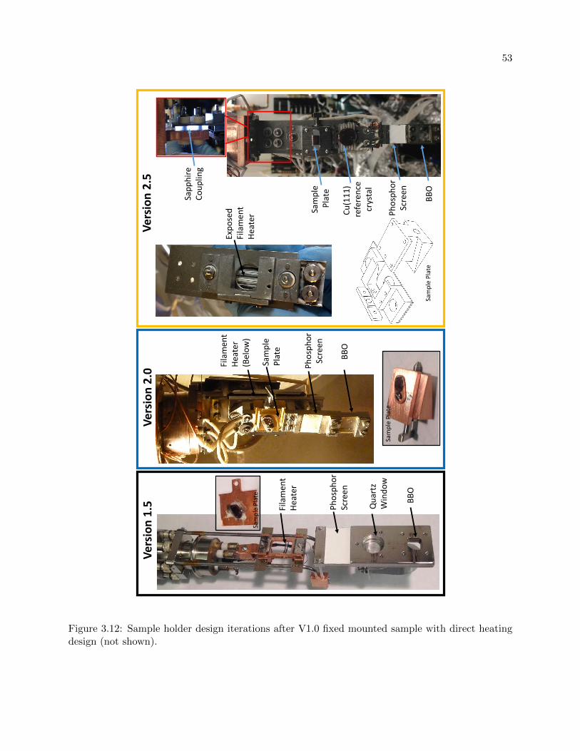
53
Vers
ion
2.0
Vers
ion
2.5
Vers
ion
1.5 Fila
men
t He
ater
Phos
phor
Scre
en
Qua
rtz
Win
dow
BBO
Expo
sed
Fila
men
t He
ater
Cu(1
11)
refe
renc
ecr
ysta
l
Phos
phor
Scre
en
BBO
Sam
ple
Plat
e
Phos
phor
Scre
en
BBO
Fila
men
t He
ater
(Bel
ow)
Sam
ple
Plat
e
Sam
ple
Plat
e
Sam
ple
Plat
e
Sam
ple
Plat
e
Sapp
hire
Co
uplin
g
Figure 3.12: Sample holder design iterations after V1.0 fixed mounted sample with direct heatingdesign (not shown).
54
(initially 995 K) and lacking of robust components and materials (brittle, work-hardened fasteners
upon annealing, degrading ceramics, and outgassing of non-high temperature materials) required
several redesigns.
The current sample holder, V2.5, has several heating improvements over the V2.0 design.
The primary improvement was the use of a tungsten filament (1600K) heater, encased in alumina
rods, with holes in the alumina to expose the bare filament towards the sample (see Fig 3.12).
With the addition of a hole in the encasing plate, this allowed for direct radiative heating of the
sample plate and was able to achieve a maximum temperature of 1250K. Heating set points was
precisely controlled using homewritten proportional- integral- derivative (PID) controlled software
interfaced with a digital DC power supply (Agilent E3634A). Similar to the V2.0 design, the cold
finger was connected to the sample holder via a sapphire coupling plate (shown in Fig 3.12, right).
Due to the > 10 x thermal conductivity of sapphire at low temperatures (50 K) compared to
high temperatures (> 300K) [59], this acted as a “one-way heat valve.” This allowed excellent
conductivity for cryogenic cooling from the cold finger to the sample mount, but poorly conducted
the localized high temperatures of the sample mount back to the cold finger. In addition to
decreasing LHe consumption from having an extra heat load, this gave more efficient cooling of the
sample upon heating and cooling cycles since the cold finger could serve as a better, more isolated
cold reservoir.
Due to the lack of rotation about either horizontal axes, accurate alignment for samples
along the correct crystalline axes, and therefore the correct cut in k-space, was a concern. This was
accomplished by either initially determining crystalline orientation through ex-situ Laue diffraction
or in-situ LEED measurements. Once the orientation was determined, the sample mounting angle
could be readjusted by either remounting the sample with silver paste (Ted Pella, Leitsilber 200
Silver Paint: V1.5) or adjusting the angle of a secondary sample plate via a screw attachment (V2
& V2.5), as seen in Fig 3.12, center.
Common to these designs was the addition of multiple diagnostic tools located directly below
the studied sample. A Cu(111) sample with secondary heater was permanently mounted to serve
55
as an in-situ diagnostic for possible issues with the analyzer due to its well established surface
preparation procedure and a well-defined band structure. After seeing any abnormalities in the
photoemission spectrum of the current studied sample, having the Cu(111) spectrum as a reference
allowed us to determine if possible issues were with the detector/systematic or with the sample
itself. A phosphor screen (P1 phosphor) was also deposited for imaging the EUV spot to aid in
fine tuning spatial overlap of the IR pump and EUV probe (as discussed in the next section). A
0.5 mm thick β-barium borate (BBO) crystal was mounted underneath this to find rough temporal
overlap between the pump and probe beams.
3.6 Finding spatial and temporal overlap
An efficient and reproducible procedure is needed in order to routinely find temporal and
spatial overlap of the EUV and IR pulses for the studies presented. This consists of primarily two
routines whereby gross adjustment is made using optical methods and fine tuning of this adjustment
accomplished through photoemission spectroscopy.
Not being able to see the EUV beam via conventional visible imaging cameras, secondary
methods are used for finding good spatial overlap of the two spots. In the EUV beam line, the Al
foil is removed and a sapphire window inserted after the red recombination chamber (to maintain
pressure differential between the mirror chamber and main chamber). Inserting the window after
the recombination chamber ensures equal additional dispersion due to the sapphire on both the
IR and EUV beams. Neutral density (ND) filters are then inserted into both beams to reduce the
intensity of the spots on the sample for better overlap of their central modes. A low lux camera
(Mintron 12V2), mounted outside a chamber viewport, is used to image the spot in the sample
plane. The residual IR of the EUV beam and IR pump beam are then overlapped on the sample.
Care is taken that the pump beam, when spatially overlapped, is still well centered on the annular
mirror in the recombination chamber otherwise mode distortions become evident. The ND filters
are then removed and the sample is vertically translated so the beams are incident on a 0.5 mm
thick BBO crystal mounted directly underneath it, on the same plane as the sample (as shown
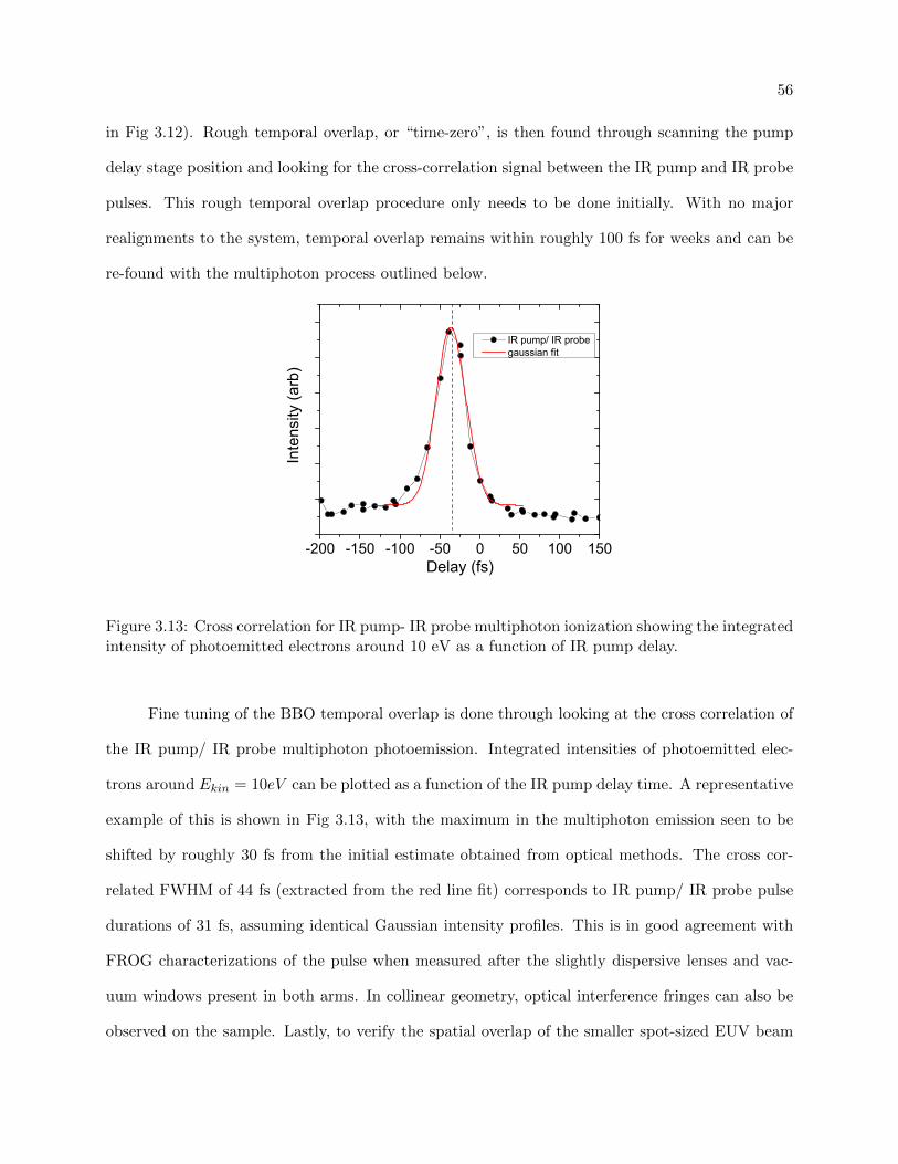
56
in Fig 3.12). Rough temporal overlap, or “time-zero”, is then found through scanning the pump
delay stage position and looking for the cross-correlation signal between the IR pump and IR probe
pulses. This rough temporal overlap procedure only needs to be done initially. With no major
realignments to the system, temporal overlap remains within roughly 100 fs for weeks and can be
re-found with the multiphoton process outlined below.
-200 -150 -100 -50 0 50 100 150
Inte
nsity
(arb
)
Delay (fs)
IR pump/ IR probe gaussian fit
Figure 3.13: Cross correlation for IR pump- IR probe multiphoton ionization showing the integratedintensity of photoemitted electrons around 10 eV as a function of IR pump delay.
Fine tuning of the BBO temporal overlap is done through looking at the cross correlation of
the IR pump/ IR probe multiphoton photoemission. Integrated intensities of photoemitted elec-
trons around Ekin = 10eV can be plotted as a function of the IR pump delay time. A representative
example of this is shown in Fig 3.13, with the maximum in the multiphoton emission seen to be
shifted by roughly 30 fs from the initial estimate obtained from optical methods. The cross cor-
related FWHM of 44 fs (extracted from the red line fit) corresponds to IR pump/ IR probe pulse
durations of 31 fs, assuming identical Gaussian intensity profiles. This is in good agreement with
FROG characterizations of the pulse when measured after the slightly dispersive lenses and vac-
uum windows present in both arms. In collinear geometry, optical interference fringes can also be
observed on the sample. Lastly, to verify the spatial overlap of the smaller spot-sized EUV beam
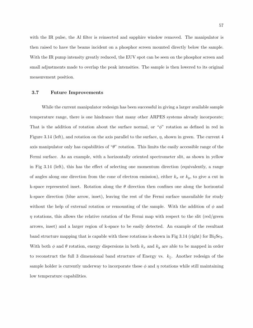
57
with the IR pulse, the Al filter is reinserted and sapphire window removed. The manipulator is
then raised to have the beams incident on a phosphor screen mounted directly below the sample.
With the IR pump intensity greatly reduced, the EUV spot can be seen on the phosphor screen and
small adjustments made to overlap the peak intensities. The sample is then lowered to its original
measurement position.
3.7 Future Improvements
While the current manipulator redesign has been successful in giving a larger available sample
temperature range, there is one hindrance that many other ARPES systems already incorporate;
That is the addition of rotation about the surface normal, or “φ” rotation as defined in red in
Figure 3.14 (left), and rotation on the axis parallel to the surface, η, shown in green. The current 4
axis manipulator only has capabilities of “θ” rotation. This limits the easily accessible range of the
Fermi surface. As an example, with a horizontally oriented spectrometer slit, as shown in yellow
in Fig 3.14 (left), this has the effect of selecting one momentum direction (equivalently, a range
of angles along one direction from the cone of electron emission), either kx or ky, to give a cut in
k-space represented inset. Rotation along the θ direction then confines one along the horizontal
k-space direction (blue arrow, inset), leaving the rest of the Fermi surface unavailable for study
without the help of external rotation or remounting of the sample. With the addition of φ and
η rotations, this allows the relative rotation of the Fermi map with respect to the slit (red/green
arrows, inset) and a larger region of k-space to be easily detected. An example of the resultant
band structure mapping that is capable with these rotations is shown in Fig 3.14 (right) for Bi2Se3.
With both φ and θ rotation, energy dispersions in both kx and ky are able to be mapped in order
to reconstruct the full 3 dimensional band structure of Energy vs. k||. Another redesign of the
sample holder is currently underway to incorporate these φ and η rotations while still maintaining
low temperature capabilities.
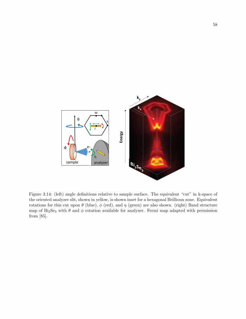
58
kx
ky
Energy
θ
φ
sample analyzer
e‐
Γ
M
K
η
Figure 3.14: (left) angle definitions relative to sample surface. The equivalent “cut” in k-space ofthe oriented analyzer slit, shown in yellow, is shown inset for a hexagonal Brillioun zone. Equivalentrotations for this cut upon θ (blue), φ (red), and η (green) are also shown. (right) Band structuremap of Bi2Se3 with θ and φ rotation available for analyzer. Fermi map adapted with permissionfrom [85].
Chapter 4
Two-Photon Photoelectron Interferometry on Cu(111)
With the realization of isolated attosecond pulses, electron dynamics measurements have
been pushed from the femtosecond to the attosecond regime. Recent experiments in time-resolved
attosecond spectroscopy have been extended to the realm of condensed matter systems, with the
hope of mapping ultrafast dynamical electronic processes akin to studies done on atomic systems
[24, 86, 87, 88]. However, benchmark studies on W(110)[89] and Mg(0001)[90] (and most recently
on Mg adlayers on W(110)[91]) employing attosecond “streaking”, where the photoemitted electron
packet traces the electric field modulation of a coincident laser pulse, have faced with the problem
of interpreting the cryptic temporal delays seen in these streaking spectra between different energy
states. Similarly seen in atomic systems like Ne [92] and in numerous atomic [93, 94, 95] and
molecular [96] systems using Attosecond Pulse Trains (APT), the quantitative interpretation of
these delays in solid state systems is still a matter of debate.
The extension of these attosecond techniques from atomic systems to surfaces is not a trivial
one. Fundamental questions about the nature of photoionization from atoms versus surfaces arise
that need to be considered experimentally and theoretically. For instance, the attosecond streaking
technique utilizes an IR field to modulate the energy of the electron in a transition between two
free states. With the presence of a surface, screening effects and standing waves of the incident
E-field can possibly distort or destroy the controlled energy modulation of the electron wavepacket
1 . Of particular interest is the delocalization of electronic states in solids. In condensed matter
1 This has been addressed on surface streaking experiments by operating at Brewster’s Angle to minimize thiseffect [89]
60
systems, 108 more atoms are probed than their atomic counterparts. Closely spaced with over-
lapping valence states, this forms a non-localized band that is difficult to model classically as a
localized electron “escaping” into the vacuum [97]. Surprisingly, however, of the limited attosecond
spectroscopy experiments that have been performed on surfaces, classical ballistic-transport models
of a localized electron traveling to the surface have worked remarkably well in reproducing observed
delays between energy bands for both localized core and delocalized valence bands.
We seek to elucidate this issue through directly probing phase delays of two conduction
bands of unique symmetry in Cu(111). We explore the nature of this photoemission by combin-
ing attosecond electron interferometry utilizing attosecond pulse trains [98, 99] with angle-resolved
photoemission. This allows us to access the phase imprinted on electrons during photoemission
from delocalized states in different conduction bands. Our data unambiguously show that pho-
toemission from the conduction band cannot be ascribed to excitation followed by semiclassical
transport of the electrons to the surface. Instead, we attribute differences due to the quantum
phase of the photoemission process that is state-dependent, notably distinguishing them from a
labeled transport “time”. These results highlight the quantum wave-like aspects of photoemission
of electrons originating in conduction bands.
In the following Chapter, the general theoretical background of attosecond spectroscopy
techniques (namely attosecond streaking and the interferometric laser-assisted technique employed
in studies here) are described in Section 4.1. The experimental technique and configuration for the
valence band study on Cu(111) is described in Sec 4.2 and 4.3. Experimental observations are then
presented in Sec 4.4, followed by a discussion in the context of previous atomic and surface studies
(Sec 4.5), with conclusions discussed in Sec 4.6.
4.1 Theoretical Background
Three unique experimental schemes can be delineated in utilizing EUV attosecond pulses
for surface spectroscopy. These approaches employ either a single EUV harmonic (Sec 4.1.1) or
multiple harmonics (Sec 4.1.2) with a coincident IR field. While most approaches were initially
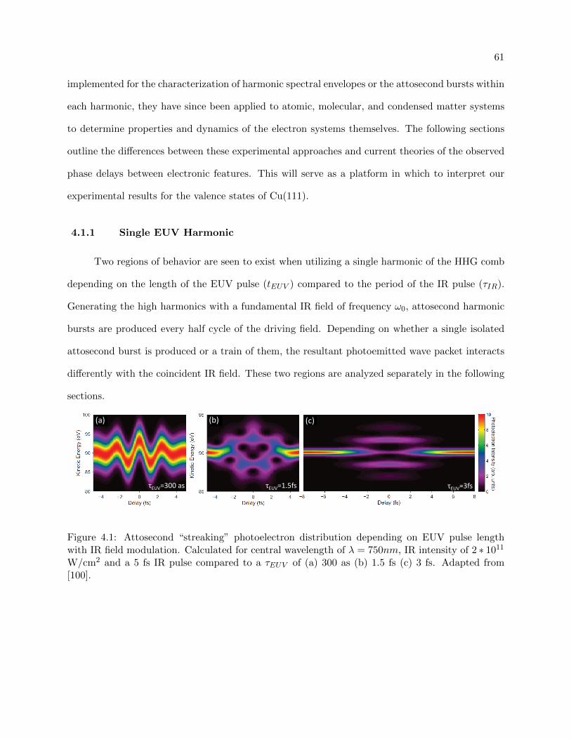
61
implemented for the characterization of harmonic spectral envelopes or the attosecond bursts within
each harmonic, they have since been applied to atomic, molecular, and condensed matter systems
to determine properties and dynamics of the electron systems themselves. The following sections
outline the differences between these experimental approaches and current theories of the observed
phase delays between electronic features. This will serve as a platform in which to interpret our
experimental results for the valence states of Cu(111).
4.1.1 Single EUV Harmonic
Two regions of behavior are seen to exist when utilizing a single harmonic of the HHG comb
depending on the length of the EUV pulse (tEUV ) compared to the period of the IR pulse (τIR).
Generating the high harmonics with a fundamental IR field of frequency ω0, attosecond harmonic
bursts are produced every half cycle of the driving field. Depending on whether a single isolated
attosecond burst is produced or a train of them, the resultant photoemitted wave packet interacts
differently with the coincident IR field. These two regions are analyzed separately in the following
sections.
(a) (b) (c)
τEUV=300 as τEUV=1.5fs τEUV=3fs
Figure 4.1: Attosecond “streaking” photoelectron distribution depending on EUV pulse lengthwith IR field modulation. Calculated for central wavelength of λ = 750nm, IR intensity of 2 ∗ 1011
W/cm2 and a 5 fs IR pulse compared to a τEUV of (a) 300 as (b) 1.5 fs (c) 3 fs. Adapted from[100].
62
4.1.1.1 “Isolated” Pulse (tEUV < τIR/2)
In the case when the EUV pulse length is less than a half cycle of the driving field, the EUV
pulse consists of only a single, isolated attosecond burst. Several different experimental approaches
exist for the actual generation of these isolated pulses including high-frequency filtering [101] and
various gating schemes of the photoionization [102] and optical [103] configuration. Once the
photoemitted wavepacket is liberated from the atom or surface, the temporal evolution of these
electrons can be reasonably understood by a semi-classical picture (for a full quantum description,
see Ref [104]). For photoionization from an atom (for simplicity), an electron’s initial momentum
can described by: pi =√
2me(~ωEUV − EB), with me being the mass of the electron, ωEUV is the
frequency of the incident EUV light, and EB is the initial binding energy (note, this would include
the work function for the case of solids). With the coincident IR field, the electron is accelerated
like a classical particle in the electric field EIR(t) polarized in the z direction. The change in
momentum for an electron emitted at time τ can be then calculated by the integrating the classical
equation of motion for the electron:
mez =− qEIR(t) = −qE0(t)cos(ωIRt+ φCE) (4.1)
mez =∆pz(τ) = −q∫ ∞τ
E0(t)cos(ωIRt+ φCE) dt (4.2)
where φCE is the carrier-envelope phase of the IR light and E0(t) follows the intensity of the
Gaussian wavepacket. Under the adiabatic approximation where, dE0/dt E0ωIR (ie. slowly
varying) the momentum can be further evaluated to:
∆pz(τ) =eE0(τ)
ωIRsin(ωIRτ + φCE) (4.3)
=√
4Up(τ)mesin(ωIRτ + φCE) (4.4)
Where Up(τ) is the pondermotive potential. Given an angle (θ) between the incident laser
polarization and z-component of momentum pz, the final momentum (pf ) and final kinetic energy
63
of the electron can be calculated.
p2f =p2
i + 2pf∆pzcosθ −∆p2z
⇒ Ekin,f =p2f
2me= Ekin,i + 2Up(τ)cos2θsin2(ωIRτ + φCE
+√
8Up(τ)Ekin,icosθsin(ωIRτ + φCE)
Assuming an experimental configuration where the laser polarization is aligned with the
z-component (θ = 0), this simplifies to a kinetic energy modulation of:
∆Ekin(τ) ≈√
8Up(τ)Ekin,isinθsin(ωIRτ + φCE) (4.5)
in the case where Ekin,i = ~ωEUV − EB Up (Up usually ∼ 50 meV for the IR intensities used
in experiments compared to 50-100 eV for ~ωEUV ). This results in a kinetic energy modulation
following the IR field modulation.
This gives the spectrogram shown in Figure 4.1(a) centered around 90 eV, where the pho-
toemitted electron packet is modulated with the IR field and is commonly referred to as attosecond
streaking. Initially applied to atomic systems, all currently published work in attosecond spec-
troscopy on solids have used this approach.
4.1.1.2 “Non-isolated” Pulse- (tEUV > τIR/2)
When the EUV pulse envelope becomes comparable or longer than a half cycle of the fun-
damental IR field, “sidebands” emerge that can be thought of as the subsequent adsorption or
emission of IR photons after direct photoemission. Shown in Figure 4.1(c), this results in a direct
photoemission peak (shown at 90 eV) flanked by sidebands of ±ω0 spacing when the IR and EUV
fields are temporally overlapped. Scanning the relative IR/EUV delay, this results in a convolution
of the IR and EUV envelopes, allowing the pulse length of the EUV wave packet to be measured
assuming an independently verified IR pulse length [105]. For comparison, the “transition region”
assuming an intermediate EUV pulse length of τEUV = 1.5fs is shown in Figure 4.1(b).
64
While not able to give attosecond temporal resolution due to the pulse length being necessarily
longer than a half IR cycle, spectroscopies in this regime have still been able to probe ultrashort
electron dynamics (as long as the dynamics as longer than the EUV pulse length). This approach has
been particularly well-suited to study inner-shell auger relaxation processes in gas phase, clocking
the time to fill the M-shell vacancy hole of the MNN Auger transition in Krypton [24], and of the
N-shell vacancy hole of the NOO Auger transition of surface-adsorbed Xe on Pt(111) [106, 107].
4.1.2 Multiple Harmonics- RABITT
An increasingly common technique using multiple harmonics has become the two-photon
photoelectron interferometry technique of RABITT (for Reconstruction of Attosecond Beating by
Interference of Two-photon Transitions) [98, 108, 99, 109]. Originally used to measure the spectral
phase of the harmonics and characterize the attosecond pulse trains [98], it has since been applied to
atomic and molecular systems to measure phase delays associated with the photoionized electrons
to give information on the systems themselves [95, 110].
In general, a comb of odd-order EUV harmonics photoionizes electrons from their initial
ground states (|g >) to produce a series of energetically equally-spaced photoemission peaks. In
the presence of an incident IR field, the energy of these EUV emitted electrons (whose state we
will deem as an intermediate state, |i >, in this two-photon process) is modulated by either the
absorption (+ω0) or emission (-ω0) of an IR photon. This yields a series of sideband peaks, denoted
final state |f >, of even harmonic order, illustrated in Fig 4.2(b). Scanning the delay of the IR pulse
with respect to the harmonic comb, τIR, the intensity of these sidebands peaks is seen to modulate
with a frequency of 2ω0, as described in depth in Section 4.1.2.1. An exemplary photoelectron
spectrum as a function of IR/EUV delay in Ar gas [112] showing this temporal modulation is seen
in Fig 4.2(a).
This technique has several advantages over the attosecond streaking approach. First, the
generation of isolated attosecond pulses requires a considerable amount more of experimental effort,
usually requiring nonlinear pulse compression techniques and a carrier-envelope phase-stabilized
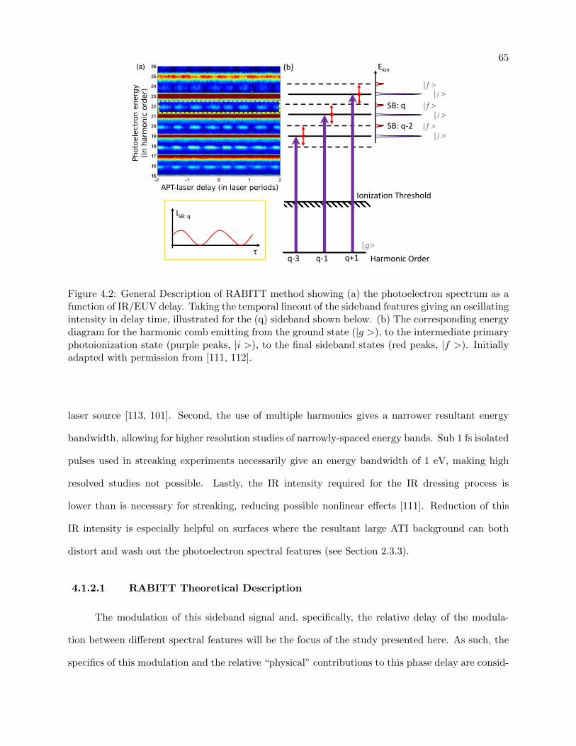
65
SB: q
SB: q‐2
Ekin
Ionization Threshold
Harmonic Orderq‐3 q‐1 q+1
(b)
ISB: q
τ|g>
|i >
|i >
|i >
|f >
|f >
|f >
Figure 4.2: General Description of RABITT method showing (a) the photoelectron spectrum as afunction of IR/EUV delay. Taking the temporal lineout of the sideband features giving an oscillatingintensity in delay time, illustrated for the (q) sideband shown below. (b) The corresponding energydiagram for the harmonic comb emitting from the ground state (|g >), to the intermediate primaryphotoionization state (purple peaks, |i >), to the final sideband states (red peaks, |f >). Initiallyadapted with permission from [111, 112].
laser source [113, 101]. Second, the use of multiple harmonics gives a narrower resultant energy
bandwidth, allowing for higher resolution studies of narrowly-spaced energy bands. Sub 1 fs isolated
pulses used in streaking experiments necessarily give an energy bandwidth of 1 eV, making high
resolved studies not possible. Lastly, the IR intensity required for the IR dressing process is
lower than is necessary for streaking, reducing possible nonlinear effects [111]. Reduction of this
IR intensity is especially helpful on surfaces where the resultant large ATI background can both
distort and wash out the photoelectron spectral features (see Section 2.3.3).
4.1.2.1 RABITT Theoretical Description
The modulation of this sideband signal and, specifically, the relative delay of the modula-
tion between different spectral features will be the focus of the study presented here. As such, the
specifics of this modulation and the relative “physical” contributions to this phase delay are consid-
66
ered in more detail. For a full theoretical description, the reader is referred to Refs [109, 114, 115].
Described using second-order perturbation theory, the total intensity for a given sideband of order
q is dependent on the two contributing “energy pathways” in the two-photon process that result in
the same sideband energy, namely the photon absorption pathway (Aabs(t)) according to ωq−1 +ω0
and the photon emission pathway (Aem(t)) according to ωq+1 − ω0. Specifically:
S(q, τ) ∝∣∣∣∣∫ +∞
+∞(Aabs(t) +Aem(t)) dt
∣∣∣∣2 (4.6)
where
Aabs(t) =∑i
〈f |−→e −→r |i〉〈i|−→e −→r |g〉εi−εg−(q−1)ω0
EIR(t− τ)EEUV (q − 1, t) eiIpt (4.7)
Aem(t) =∑i
〈f |−→e −→r |i〉〈i|−→e −→r |g〉εi−εg−(q+1)ω0
E∗IR(t− τ)EEUV (q + 1, t) eiIpt (4.8)
with Ip being the ionization potential, −→e is the common polarization between the EUV and IR
field, τ is the relative delay between the IR and EUV fields, and εi and εg are the corresponding
energies of the |i > and |g > states, respectively. EIR and EEUV are the complex representations
of the IR and EUV fields given in by:
EEUV (q, t) = Eqe−iqω0t−φq (4.9)
EIR(q, t) = Ee−iω0t (4.10)
With Eq and E being the amplitude of the harmonics and IR fields, respectively and φq being the
relative phase of the qth harmonic. The complicated summation term over intermediate states in
Eqs 4.7 and 4.8 only contributes at energies corresponding to the two quantum pathways that lead
to the final state energy, namely εi = εq + (q± 1)ω0. For simplicity, these summation terms can be
written in complex form:
Aq−1abs e
iφq−1abs =
∑i
〈f |−→e −→r |i〉〈i|−→e −→r |g〉εi−εg−(q−1)ω0
(4.11)
Aq−1em eiφ
q+1abs =
∑i
〈f |−→e −→r |i〉〈i|−→e −→r |g〉εi−εg−(q+1)ω0
(4.12)
Making the assumption that there is little variation in intensity between the (q − 1) and (q + 1)
harmonics (Eq−1 = Eq+1), we can substitute Eq 4.11 and 4.12 into Eq 4.7 and 4.8 to obtain a
67
reduced expression for Eq 4.6:
S(q, τ) ∝M∣∣∣∣∫ +∞
+∞(EIREqe
iqω0t+iIpt) dt
∣∣∣∣2 (4.13)
where
M =∣∣∣Aq−1
abs eiφq−1
abs exp(iφq−1abs − iφq−1 + iω0t) +Aq−1
em eiφq+1abs eiφ
q+1abs exp(iφq+1
abs − iφq+1 + iω0t)∣∣∣2 (4.14)
With the introduction of terms S0 =∣∣∣Aq−1
abs
∣∣∣2 +∣∣∣Aq+1
em
∣∣∣2 and S1 = 2√Aq−1abs A
q+1em , Eq 4.13 simplifies
to an easier to interpret expression:
S(q, τ) ∝ S0 + S1cos(∆φatq + ∆φq + 2ω0τ) (4.15)
Where ∆φatq = φq+1em −φq−1
abs is deemed the “atomic” phase difference, to be discussed further,
and ∆φq = φq+1 − φq−1 is the phase difference between consecutive harmonics.
This demonstrates that the sideband amplitude should oscillate with 2ω0 as a function of
temporal delay. It should be noted that a simple optical interference of the IR pulses would result
in a 1ω interference, as seen in Appendix A.2. With measurement of the harmonic phase difference
being the original motivation for the RABITT technique [98], initial estimates for contribution of
the atomic phase difference were small and therefore ignored. However, recent gas and molecular
phase experiments have found phase shifts where a non-negligible contribution can be attributed
to this atomic phase. Due to its importance in interpreting our results in the present study, more
detail on this atomic phase and this class of experiments will be given in the following section.
4.1.2.2 RABITT Studies on Atomic & Molecular Systems
Studies applying this interferometric RABITT technique to atomic and molecular systems
have noticed delays in the observed interferogram between different energy states. By recording
the photoelectron interferograms of different energy states simultaneously with, for example, a
wide energy-acceptance time-of-flight detector, the group delay term in Eq 4.15 is identical and
all observed changes between states can be attributed to the atomic delay, φatq . Studies on Argon
using RABITT revealed a delay of up to 110 as between the 3p and 3s states [95]. Subsequent
68
studies on Helium [93] and molecular Nitrogen [96] then observed large phase differences when their
intermediate (|i >) direct photoionization state was resonant with a direct transition, theoretically
ramping through a π phase shift over the resonance.
With the ability to measure this atomic phase contribution directly, its helpful to understand-
ing the observed phase delays by determining what physical effects this term can be attributed to.
In the theoretical description given in Section 4.1.2.1, any hint as to what actually contributes to
the total φatq was hidden due to not assuming any specific form for the wavefunctions of the states
themselves (we only assumed an amplitude and phase for the absorption and emission pathways in
Eq 4.11 and 4.12). Theory has since been done expanding the |g >,|i >, and |f > wavefunctions
into partial waves and analyzing the radial part of the two-photon transition matrix element. While
the details of the derivation can be found elsewhere [95, 111], its worth analyzing the resultant “re-
cast” form of the transition matrix elements seen in Eq 4.7 and 4.8. For the absorption case in
momentum space, this gives:
Aabs(k) ∝ eiηl(ka)︸ ︷︷ ︸I
×( i
ka − k
)iz (2k)i/k
(2ka)i/kaΓ(2 + iz)︸ ︷︷ ︸
II
(4.16)
where z = 1/ka − 1/k, ka is the momentum associated with the photon absorption pathway, ηl is
the scattering phase of the final state, and Γ(k) is the complex gamma function. Analyzing each
piece: (I) describes the scattering phase of the intermediate state while the phase of (II) is associ-
ated with the laser-driven transition from the intermediate to final continuum states (“continuum-
continuum”) in the presence of the long range Coulomb potential, φcca . Taking into account the
absorption and emission pathways then, this gives a total expression for the atomic phase being
comprised of:
τat =ηl(ke)− ηl(ka)
2ω︸ ︷︷ ︸τW
+φcce (k)− φcca (k)
2ω︸ ︷︷ ︸τCC
(4.17)
In summary then, the two resultant terms can be thought of as:
• τW : A Wigner delay of the single-photon photoionization or the delay of the photoelectron
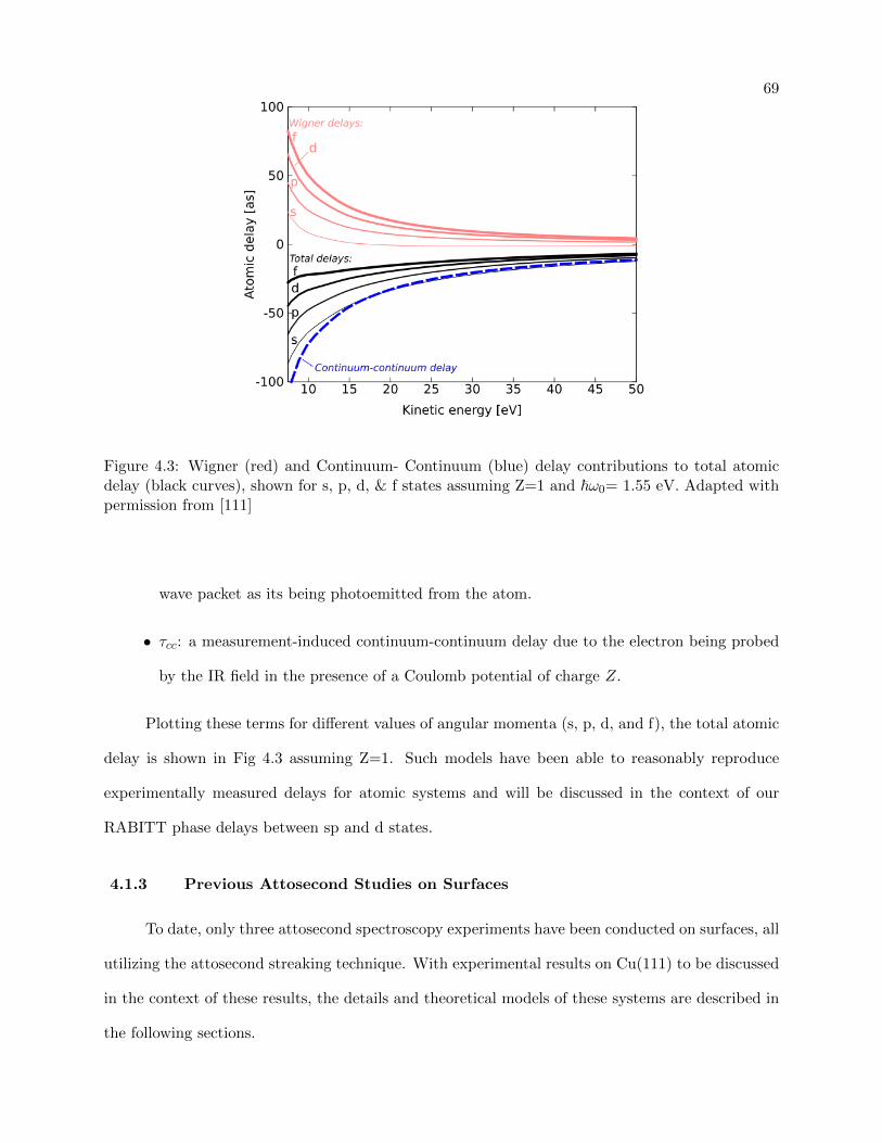
69
Figure 4.3: Wigner (red) and Continuum- Continuum (blue) delay contributions to total atomicdelay (black curves), shown for s, p, d, & f states assuming Z=1 and ~ω0= 1.55 eV. Adapted withpermission from [111]
wave packet as its being photoemitted from the atom.
• τcc: a measurement-induced continuum-continuum delay due to the electron being probed
by the IR field in the presence of a Coulomb potential of charge Z.
Plotting these terms for different values of angular momenta (s, p, d, and f), the total atomic
delay is shown in Fig 4.3 assuming Z=1. Such models have been able to reasonably reproduce
experimentally measured delays for atomic systems and will be discussed in the context of our
RABITT phase delays between sp and d states.
4.1.3 Previous Attosecond Studies on Surfaces
To date, only three attosecond spectroscopy experiments have been conducted on surfaces, all
utilizing the attosecond streaking technique. With experimental results on Cu(111) to be discussed
in the context of these results, the details and theoretical models of these systems are described in
the following sections.
70
4.1.3.1 Experimental Studies
In a benchmark study on W(110) [89], Cavalieri et al. used attosecond streaking to observe
a phase delay in the streaking spectrograms between the conduction band and the 4f core state.
Generating 300 as isolated pulses via high harmonic generation in Neon using a 5fs, 750 nm centered
laser-pulse, emitted photoelectrons up to 88 eV kinetic energy were detected using a time-of-flight
spectrometer. Comparing to the streaking spectra of the conduction band, the spectrogram for the
4f electrons were shifted 110 ± 70 as. This delay was initially attributed to transport of the core
electrons to the surface, due to the mean free path of the core electrons being 1A longer.
A subsequent study on Mg(0001) [90] demonstrated little to no delay between the valence
band spectrogram and the 2p state, within the experimental error of ±20 as. Due to the final
excited states within the crystal being well approximated by a free-electron parabola, free-particle
velocities for both the valence and core electrons could be calculated. Taking into account the
varying escape depths of the two states, the modeled ballistic propagation time was found to be
identical between the states, yielding the negligible observed delay.
Most recently, this work has been extended to observed “controllable” attosecond delays
between (1) the conduction band and Mg 2p state and (2) W 4f and Mg 2p state with the addition
of Mg adlayers on W(110)[91]. With additional monolayers of Magnesium, the observed time delay
in the underlying Tungsten and conduction band states was progressively increased. For the 4f
core level delay, a transport model similar to that applied in Mg(0001) studies [90] yielded good
experimental agreement. They additionally found that the IR dressing field was screened almost
completely within the first atomic overlayer of Mg. Surprisingly, the delocalized conduction band
delay was reproduced with the same classical transport model, after properly weighting the Mg
and W contributions to the blurred, joint conduction band.
71
4.1.3.2 Theoretical Models
More closely analyzing the contributions to the RABITT atomic delay seen in Eq 4.16, the
streaking delay in atomic systems can be described by the contribution of two factors: a “Wigner
time delay” (τW ) associated with the group delay of the photoelectrons and a “Coulomb-laser
coupling” delay (τCLC that describes the IR field interaction with the ionic Coulomb potential. In
total then, this streaking time delay is represented as:
τstreaking = τW + τCLC (4.18)
and has been extensively modeled for atomic systems with various modifications to the core po-
tential (CLC term) [116, 92] to explain the 21 ± 5 as time delay in Neon between the 2p and 2s
electrons [92]. However, these models were only able to account for less than half of the observed
delay, leaving the full theoretical description still actively explored. It should be noted that the
τCLC term in Eq 4.18 and the τCC term described in Eq 4.16, while introduced in the separate
contexts of attosecond streaking and RABITT, respectively, equivalently describe the two-photon
IR/EUV interaction [117, 111].
Present models to explain the observed attosecond delays in solids have applied a wide range
of approaches from quantum mechanical to classical, including: direct calculation of dipole matrix
element phases while accounting for the degree of localization of the initial state wavefunctions [118],
applying a jellium model [119] accounting for wavefunction localization [120, 121], and classical
ballistic-like theories of electron transport to the surface. These classical models have taken into
consideration the group velocities for the initial [122] and final [89] states. Somewhat surprisingly,
the simple ballistic transport model has worked exceptionally well in describing the phase delay
behavior of the localized core-levels. In W(110), the 110 as delay of the 4f state compared to
the valence band (VB) electrons has shown reasonable quantitative agreement with such models
[89, 122], along with the lack of delay (< 20 as) seen between the VB and 2p electrons in Mg(0001)
[90]. The delocalized nature of the valence bands, however, has proved a challenge to agree on a
well-suited description. Recent results for the VB phase delay in Mg/W(110) have been reproduced
72
with ballistic models [91] even though theories have suggested them to be ill-suited for describing
delocalized states [121, 123]. This suggests a more intricate interpretation of these delays is required
and the need for further experimental systems.
4.2 RABITT on Surfaces
Illustrated for the case of bulk (sp & d states, blue) and surface-state (green) electrons, once
photoemitted using EUV light, electrons are modulated by the coincident IR field, illustrated in
electron kinetic energy in Figure 4.4, left. This gives rise to “sideband features bracketing the
original photoelectron energy at ±ω corresponding to simultaneous absorption and emission of
IR photons, taking place after the electron has reached a final state in the continuum [105, 124].
When using the comb of harmonics, the detected photoemission spectra feature a manifold of
equidistant one-photon photoemission peaks (shown in black, for surface and valence states), with
intensity modified by the incident HHG intensity and any changing photoemission cross-sections,
and two-photon sideband peaks (red peaks) formed by contributions from neighboring harmonics.
The magnitude and shape of these sidebands are modulated as the time delay between the HHG
and laser beams is changed (illustrated top right for sp & d state sideband features), encoding
temporal information about emission from the underlying initial electronic state [93, 95, 96]. If
the HHG waveform consists of an isolated attosecond burst, then the energy of the photoelectrons
are streaked, as in the experimental studies mentioned previously. These oscillations and, more
specifically, the nature of observed phase delays (∆φ) between sidebands corresponding to different
electronic states be will be the central focus in the following discussions.
4.2.1 Surface States
Due to the termination of the solid by the surface, new electronic states are allowed that are
not present in an ideal infinite solid. These states are localized around the surface and decay into
vacuum. If its energy lies within the band gap, these states are discrete and the wave function
decays exponentially into the bulk as well. Otherwise, they have a linewidth due to hybridization
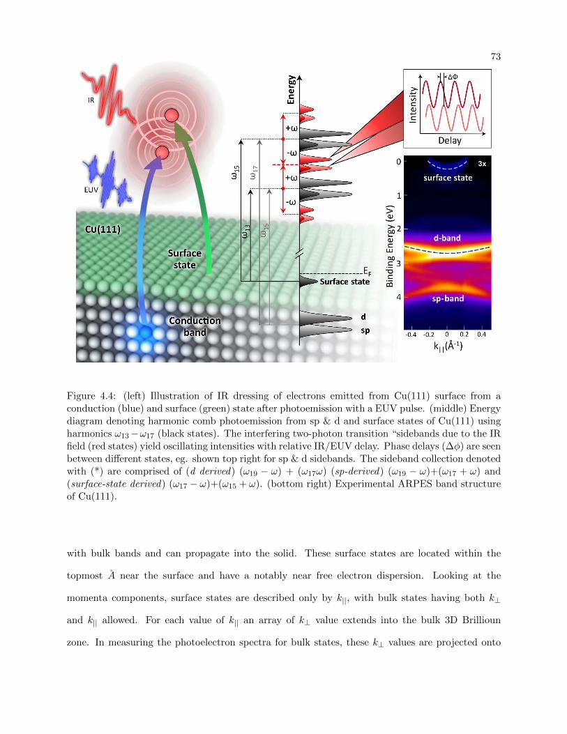
73
Figure 4.4: (left) Illustration of IR dressing of electrons emitted from Cu(111) surface from aconduction (blue) and surface (green) state after photoemission with a EUV pulse. (middle) Energydiagram denoting harmonic comb photoemission from sp & d and surface states of Cu(111) usingharmonics ω13−ω17 (black states). The interfering two-photon transition “sidebands due to the IRfield (red states) yield oscillating intensities with relative IR/EUV delay. Phase delays (∆φ) are seenbetween different states, eg. shown top right for sp & d sidebands. The sideband collection denotedwith (*) are comprised of (d derived) (ω19 − ω) + (ω17ω) (sp-derived) (ω19 − ω)+(ω17 + ω) and(surface-state derived) (ω17 − ω)+(ω15 + ω). (bottom right) Experimental ARPES band structureof Cu(111).
with bulk bands and can propagate into the solid. These surface states are located within the
topmost A near the surface and have a notably near free electron dispersion. Looking at the
momenta components, surface states are described only by k||, with bulk states having both k⊥
and k|| allowed. For each value of k|| an array of k⊥ value extends into the bulk 3D Brillioun
zone. In measuring the photoelectron spectra for bulk states, these k⊥ values are projected onto
74
the measured k|| value. Due to the sole k|| component for the surface state, it should not disperse
with k⊥ as photon energy is varied.
4.2.2 Cu(111) Band structure
ARPES spectra were recorded along the ΓM line of the surface-projected Brillouin zone,
shown in Fig 4.4 (right) using the He Iα line from a helium discharge source, and an acceptance
cone of ±6 in a 2D electron analyzer in order to map the dispersion (energy, E vs momentum, k||)
of the valence states of Cu(111). Three distinct spectral features can be observed near the k||=0
(Γ) point. The d & sp bands appear at energies around 2.9 eV and 3.8 eV below the Fermi level,
respectively, while the Shockley surface state appears near the Fermi level, in the surface projected
band gap of Cu(111) at ∼0.4 eV [125, 69, 126, 127].
The two valence states have notably different symmetries, with the d band having Λ3 sym-
metry while the sp band is comprised of two weaker states of Λ1 and Λ3 symmetry that mix near
Γ and split at higher momenta. This is shown in the band diagram in Fig 4.5(left, top) with the
experimental band structure for the full Brillouin zone shown bottom. The state of symmetry Λ1
dominates the photoelectron signal around the lower momenta range investigated here, as evident
in polarization measurements, where the sp band has a strong polarization dependence between s
and p polarizations. The d state with dominant Λ3 symmetry has little to no polarization depen-
dence. The surface state also is seen to have higher emission for p-polarized light, indicative of a
more Λ1 symmetry (often described as a sp- derived surface state).
4.3 Experimental Configuration
To generate the high harmonic and infrared laser fields, we used a multipass Ti:Sapphire
amplifier delivering 0.8 mJ pulses at a repetition rate of 5 kHz (pulse duration 25 fs and central
wavelength 790 nm). The output of the amplifier was divided into two phase locked beams and
actively stabilized. Approximately 90 % of the laser output was focused into a 250 µm inner-
diameter waveguide filled with Kr gas at a pressure of 14 Torr, to generate a comb of five p-
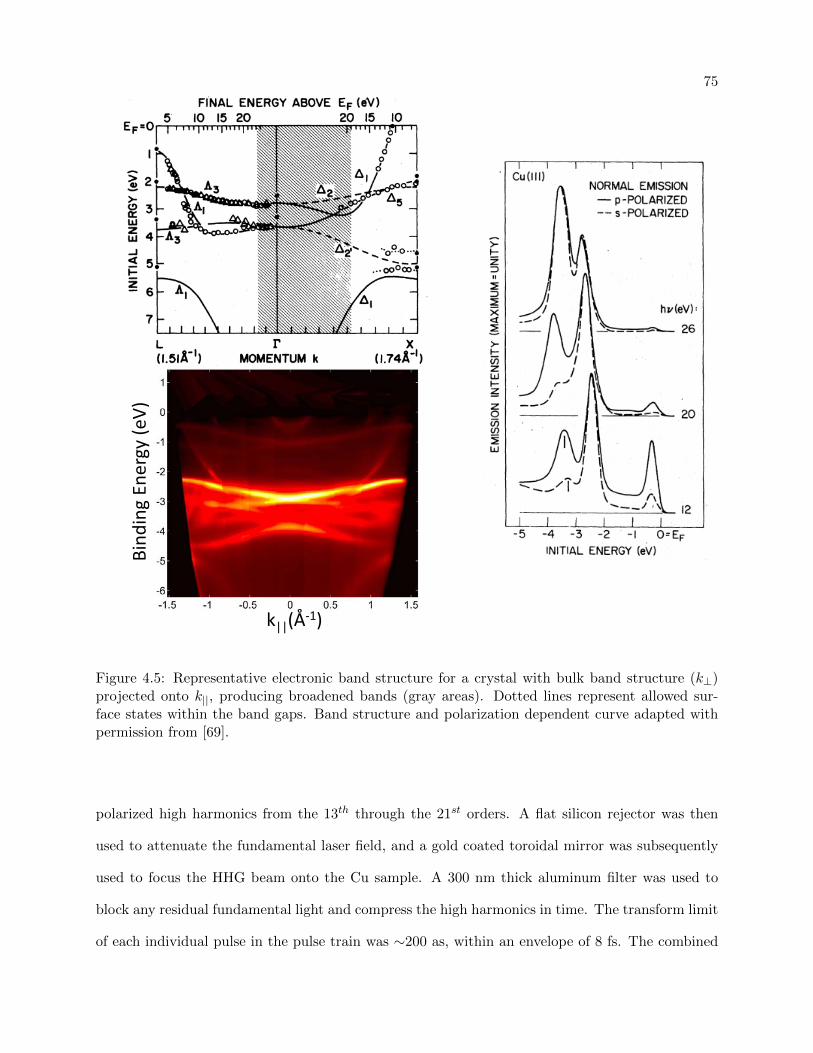
75
k||(Å‐1)
Bind
ing Energy (e
V)
Figure 4.5: Representative electronic band structure for a crystal with bulk band structure (k⊥)projected onto k||, producing broadened bands (gray areas). Dotted lines represent allowed sur-face states within the band gaps. Band structure and polarization dependent curve adapted withpermission from [69].
polarized high harmonics from the 13th through the 21st orders. A flat silicon rejector was then
used to attenuate the fundamental laser field, and a gold coated toroidal mirror was subsequently
used to focus the HHG beam onto the Cu sample. A 300 nm thick aluminum filter was used to
block any residual fundamental light and compress the high harmonics in time. The transform limit
of each individual pulse in the pulse train was ∼200 as, within an envelope of 8 fs. The combined
76
experimental energy resolution was < 180 meV.
The dressing infrared beam was adjustable in energy up to ∼ 12 µJ/pulse. The HHG and
infrared beams were recombined using an annular silver mirror. The harmonics passed through the
central hole while 60% of the incident IR beam was reflected and focused at an angle of 45 degree
to a spot size of 180 µm onto the sample. The pump-probe delay was controlled using a stepper
motor calibrated with an external interferometer. Annular portions of the IR components of both
beams were used in this interferometer for in-situ diagnostics of the time delay.
An atomically clean Cu(111) surface was prepared in a UHV chamber (base pressure 6∗10−10
Torr) by cycles of sputtering at room temperature (using 0.5 keV argon ions at 60 degree incidence
angle at the surface), followed by annealing at 820 K for 10 minutes. Only surfaces exhibiting
sharp low-energy electron diffraction patterns and narrow Shockley surface state, as verified by
PES, were used for our time-resolved experiments. Static photoelectron spectra were measured
using the helium discharge source operating at 21 eV the hemispherical photoelectron analyzer
(acceptance angle set to ±6 at all times). Time-resolved measurements were performed in the
same chamber, with a voltage of 3 V applied to sample at all times. Spectra presented here have
been energy-corrected for this applied bias.
4.4 Experimental Results
Figure 4.6 plots the photoelectron emitted via the harmonic comb at snapshots in time to
highlight the appearance of IR generated sidebands. The spectra in Fig 2b is collected when the
IR laser arrives 1000 fs before (defined as negative time) the HHG comb, so that no IR modulation
is expected. Due to the harmonic spacing and spacing of the sp & surface state, at the point, the
surface state peak from the (2n − 1)th harmonic overlaps with the sp band from the (2n + 1)th
harmonic [Figs. 4.6(b) and (c)]. However, since the surface state exists only in a finite range
of momenta around [indicated by the oval regions in Fig. 4.6(b), 0 ≤ k|| ≤ ±0.15A−1], and we
employ momentum-resolved detection, we can collect photoelectrons at higher momenta where the
different states do not overlap. This allows for simultaneous study of sideband features for the sp,
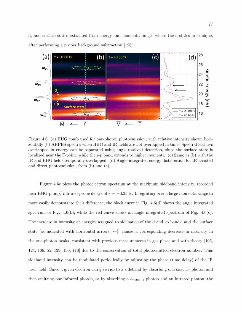
77
d, and surface states extracted from energy and momenta ranges where these states are unique,
after performing a proper background subtraction [128].
16
18
20
22
24
26
28τ = +0.65 fs
ω15
ω17
ω19
ω21
(c)(a) (d)
ΓM
τ = ‐1000 fsτ = +0.65 fs
Kinetic Energy (eV)
τ = ‐1000 fs
Surface states‐p
d
ω13
ω15
ω17
ω19
(b)
ΓM
Figure 4.6: (a) HHG comb used for one-photon photoemission, with relative intensity shown hori-zontally (b) ARPES spectra when HHG and IR fields are not overlapped in time. Spectral featuresoverlapped in energy can be separated using angle-resolved detection, since the surface state islocalized near the Γ-point, while the s-p band extends to higher momenta. (c) Same as (b) with theIR and HHG fields temporally overlapped. (d) Angle-integrated energy distribution for IR-assistedand direct photoemission, from (b) and (c).
Figure 4.6c plots the photoelectron spectrum at the maximum sideband intensity, recorded
near HHG-pump/ infrared-probe delays of τ = +0.35 fs. Integrating over a large momenta range to
more easily demonstrate their difference, the black curve in Fig. 4.6(d) shows the angle integrated
spectrum of Fig. 4.6(b), while the red curve shows an angle integrated spectrum of Fig. 4.6(c).
The increase in intensity at energies assigned to sidebands of the d and sp bands, and the surface
state [as indicated with horizontal arrows, ←], causes a corresponding decrease in intensity in
the one-photon peaks, consistent with previous measurements in gas phase and with theory [105,
124, 106, 55, 129, 130, 110] due to the conservation of total photoemitted electron number. This
sideband intensity can be modulated periodically by adjusting the phase (time delay) of the IR
laser field. Since a given electron can give rise to a sideband by absorbing one ~ω2m+1 photon and
then emitting one infrared photon, or by absorbing a ~ω2m−1 photon and an infrared photon, the
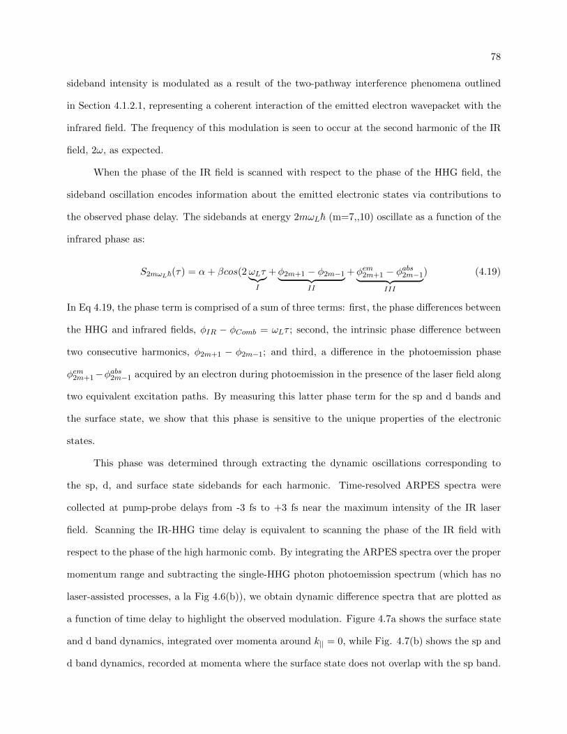
78
sideband intensity is modulated as a result of the two-pathway interference phenomena outlined
in Section 4.1.2.1, representing a coherent interaction of the emitted electron wavepacket with the
infrared field. The frequency of this modulation is seen to occur at the second harmonic of the IR
field, 2ω, as expected.
When the phase of the IR field is scanned with respect to the phase of the HHG field, the
sideband oscillation encodes information about the emitted electronic states via contributions to
the observed phase delay. The sidebands at energy 2mωL~ (m=7,,10) oscillate as a function of the
infrared phase as:
S2mωL~(τ) = α+ βcos(2 ωLτ︸︷︷︸I
+φ2m+1 − φ2m−1︸ ︷︷ ︸II
+φem2m+1 − φabs2m−1︸ ︷︷ ︸III
) (4.19)
In Eq 4.19, the phase term is comprised of a sum of three terms: first, the phase differences between
the HHG and infrared fields, φIR − φComb = ωLτ ; second, the intrinsic phase difference between
two consecutive harmonics, φ2m+1 − φ2m−1; and third, a difference in the photoemission phase
φem2m+1−φabs2m−1 acquired by an electron during photoemission in the presence of the laser field along
two equivalent excitation paths. By measuring this latter phase term for the sp and d bands and
the surface state, we show that this phase is sensitive to the unique properties of the electronic
states.
This phase was determined through extracting the dynamic oscillations corresponding to
the sp, d, and surface state sidebands for each harmonic. Time-resolved ARPES spectra were
collected at pump-probe delays from -3 fs to +3 fs near the maximum intensity of the IR laser
field. Scanning the IR-HHG time delay is equivalent to scanning the phase of the IR field with
respect to the phase of the high harmonic comb. By integrating the ARPES spectra over the proper
momentum range and subtracting the single-HHG photon photoemission spectrum (which has no
laser-assisted processes, a la Fig 4.6(b)), we obtain dynamic difference spectra that are plotted as
a function of time delay to highlight the observed modulation. Figure 4.7a shows the surface state
and d band dynamics, integrated over momenta around k|| = 0, while Fig. 4.7(b) shows the sp and
d band dynamics, recorded at momenta where the surface state does not overlap with the sp band.
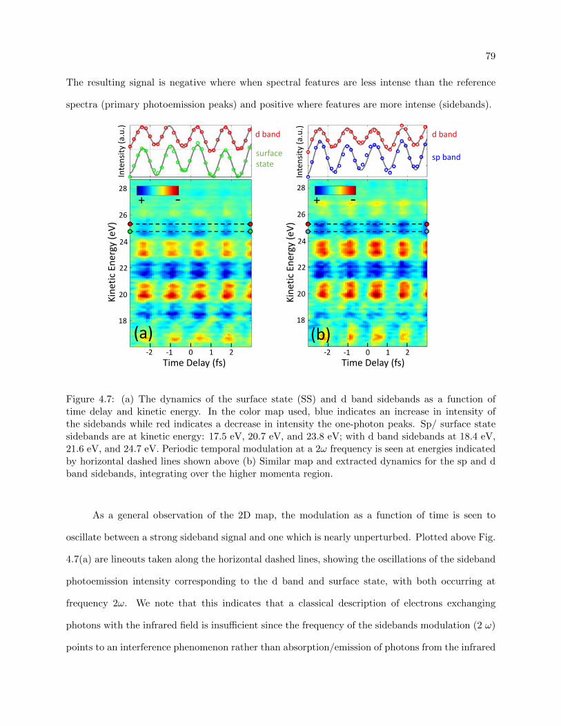
79
The resulting signal is negative where when spectral features are less intense than the reference
spectra (primary photoemission peaks) and positive where features are more intense (sidebands).
18 20 22 24
-100
0
100
200
transport
d band
sp band
-0.4
0.0
0.4
0.8
15 17 19
-0.4
0.0
0.4
0.8
-100
0
100
200
Phase Diffe
rence (rad) (c)
Electron Kinetic Energy (eV)
(a) (b)
+ ‐ + ‐
(d) φ(d‐sp)
Phase Diffe
rence (rad)
Harmonic Order (ω)
Phase Difference (as)Phase Difference (as)
d band
sp bandsurfacestate
d band φ(d‐ss)
Kine
tic Ene
rgy (eV)
Kine
tic Ene
rgy (eV)
Intensity
(a.u.)
Intensity
(a.u.)
Time Delay (fs) Time Delay (fs)‐2 ‐1 0 1 2 ‐2 ‐1 0 1 2
24
18
20
22
26
28
24
18
20
22
26
28
φ(sp‐ss)
Figure 4.7: (a) The dynamics of the surface state (SS) and d band sidebands as a function oftime delay and kinetic energy. In the color map used, blue indicates an increase in intensity ofthe sidebands while red indicates a decrease in intensity the one-photon peaks. Sp/ surface statesidebands are at kinetic energy: 17.5 eV, 20.7 eV, and 23.8 eV; with d band sidebands at 18.4 eV,21.6 eV, and 24.7 eV. Periodic temporal modulation at a 2ω frequency is seen at energies indicatedby horizontal dashed lines shown above (b) Similar map and extracted dynamics for the sp and dband sidebands, integrating over the higher momenta region.
As a general observation of the 2D map, the modulation as a function of time is seen to
oscillate between a strong sideband signal and one which is nearly unperturbed. Plotted above Fig.
4.7(a) are lineouts taken along the horizontal dashed lines, showing the oscillations of the sideband
photoemission intensity corresponding to the d band and surface state, with both occurring at
frequency 2ω. We note that this indicates that a classical description of electrons exchanging
photons with the infrared field is insufficient since the frequency of the sidebands modulation (2 ω)
points to an interference phenomenon rather than absorption/emission of photons from the infrared
80
field (frequency of ω). Similar temporal lineouts are shown for the high momenta extracted region
in Fig 4.7 (b) to give interferograms for the d band and sp band features.
The intensity modulation of sidebands from the sp, d, and surface states are similar to that
shown above in Fig. 4.7(a) & (b) - but all show different phase offsets. Fourier analysis was used
to extract the phases of all of the sidebands. For a more detailed discussion of the extraction
technique, see Appendix A.4. For the surface state, the sum of the HHG and the photoemission
phase terms increases monotonically with energy [as shown in Fig. 4.8a], consistent with previous
measurements in gases [99, 110, 130]. This phase is indicative of the atto-chirp present on the HHG
comb.
The two conduction band features are then compared in two ways: (1) Using the surface
state interferogram as a benchmark (Fig 4.8 b) in order to use the localized surface emission from
the surface state electrons as a “start time” to our classical electron transport clock, as proposed
by Ref [119], and (2) comparing the d band emission benchmarked to the sp band (Fig 4.8 c). In
Fig 4.8 b, while both exhibit an almost linear decrease as a function of increasing kinetic energy,
the phase of the d sideband at the lowest kinetic energy is notably larger (0.88 ± 0.05) rad than the
corresponding phase of the sp sideband (0.39 ± 0.05) rad. In addition, at highest kinetic energies,
both the sp and d sidebands have negative phases, i.e. (-0.38 ± 0.12) rad and (-0.18 ± 0.12) rad,
respectively.
4.5 Discussion
The linear behavior of the sp and d band photoemission phase seen in Fig. 4.8 might suggest
that a classical transport mechanism of the conduction electrons to the surface, giving rise to a
time/phase delay. Assuming an electron escape depth λe = 6A for Cu(111), we estimate a transit
time of 95 as for photoelectrons of the lowest kinetic energy shown in Fig. 4.8. The corresponding
transport time for the highest kinetic energy electrons yields 85 as, for a total change in delay of
∼10 as over the kinetic energy range probed. The d-band phase delay is actually observed to change
∼250 as over the KE range. It should be noted that the difference in transport time between the
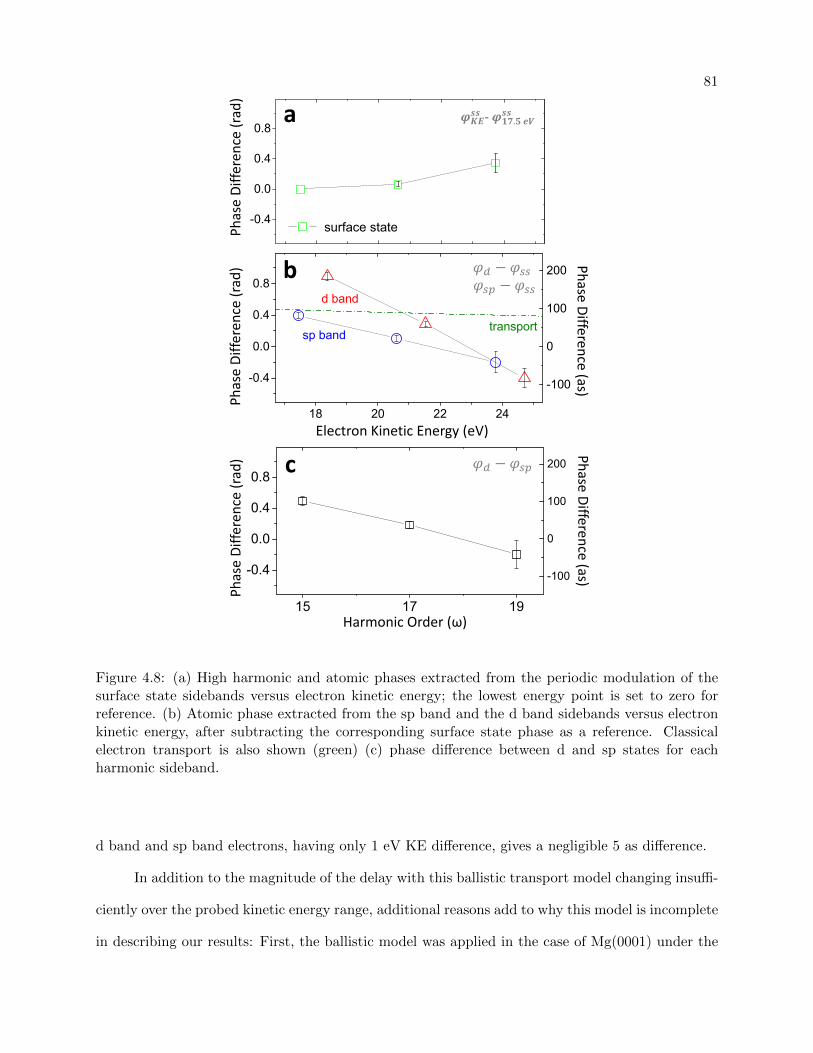
81
surface state-0.4
0.0
0.4
0.8‐ .
18 20 22 24
-100
0
100
200
transport
d band
sp band
-0.4
0.0
0.4
0.8
15 17 19
-0.4
0.0
0.4
0.8
-100
0
100
200
Phase Diffe
rence (rad)
Phase Diffe
rence (rad)
Phase Difference (as)Phase Difference (as)
Phase Diffe
rence (rad)
a
b
cElectron Kinetic Energy (eV)
Harmonic Order (ω)
Figure 4.8: (a) High harmonic and atomic phases extracted from the periodic modulation of thesurface state sidebands versus electron kinetic energy; the lowest energy point is set to zero forreference. (b) Atomic phase extracted from the sp band and the d band sidebands versus electronkinetic energy, after subtracting the corresponding surface state phase as a reference. Classicalelectron transport is also shown (green) (c) phase difference between d and sp states for eachharmonic sideband.
d band and sp band electrons, having only 1 eV KE difference, gives a negligible 5 as difference.
In addition to the magnitude of the delay with this ballistic transport model changing insuffi-
ciently over the probed kinetic energy range, additional reasons add to why this model is incomplete
in describing our results: First, the ballistic model was applied in the case of Mg(0001) under the
82
assumption that the final excited states within the crystal were free-electron like in their dispersion.
This allowed the electron to be modeled as a freely propagating particle within the material. In
the case of Cu(111), excited final states are not free-electron like, voiding the model’s applicability.
Secondly, no parameter within the transport model can account for differences between the sp and
d states. Qualitatively, they are similarly delocalized and their small binding energy difference
yields a minimal transport time delay (5 as).
A natural comparison for these results is to look at the case of delays observed using RABITT
on atomic systems, where a classical transport model of electrons is inherently not applicable. As
introduced in Section 4.1.2.2, models on atomic systems identified two contributions to the observed
phase delay: a Wigner phase and continuum-continuum phase. While there is no obvious analogue
of delocalized valence states for atomic systems, applying this atomic model in the case of s, p,
and d electrons for Copper atoms demonstrates a diminishing phase difference between these states
as a function of increasing kinetic energy (see Fig 4.3). To first order then, this reproduces the
diminishing phase difference between the d and sp states in the case of the solid (Fig 4.8c). This
demonstrates that, while screening and other solid state effects are not accounted for, the dominant
factor governing these delays is akin to the atomic case and the due to the properties of the states
themselves. We expect with full time dependent density functional calculations (TD-DFT) that
properly simulate the crystalline potential and wavefunctions, this phase difference will be accounted
for entirely.
One remaining question is then, how do we rectify the core level and valence states being
adequately modeled by ballistic transport in these other experimental systems? Agreeing with
the most extensive quantum mechanical theory that localization of the wavefunction needs to
be taken into account, its not difficult to argue that the localized core level wavefunctions can
be approximated as classically propagating particles. In the case of the valence state, why the
transport model may still adequately hold can be seen in the details of the experimental approach
in the Mg adlayers on W(110). Modeling of the IR field within the metal demonstrated near
complete damping after the first atomic layer. This means that the effect of the streaking field was
83
negligible before the electrons had escaped into the vacuum. Therefore, the delocalized valence
state was essentially confined in space to the first atomic layer. This effective localization of the
state might then allows the transport model give reasonable experimental agreement. In our case of
Copper, this does not hold, since the infrared skin depth is large compared to the electron escape
depth (δIR ∼ 100A)[131, 132]. While the dominant contribution to the photoemission signal is
from the surface (see Appendix A.3) the delocalized electrons are dressed within a larger extent of
the solid.
4.6 Conclusions
We have used the interferometric attosecond technique of RABITT to study two unique
valence states of Cu(111), observing a phase difference between them. We interpret this phase
delay as being intrinsically linked to properties of the bands themselves, such as symmetry and
dispersion, with the magnitude not fully explained in the context of a classical ballistic transport
model. Finally, our measurements demonstrate the first example of applying this interferometric
attosecond technique to surfaces, illuminating new possibilities to measuring coherent phenomena
in materials without the need for isolated attosecond pulses. We expect these results to provide a
wider context in which to interpret previous attosecond delays in condensed matter systems and
to serve as a test case for more through Quantum Mechanical modeling of interferometric delays
on surfaces.
Chapter 5
Graphene
With the still relatively recent experimental realization of Graphene [133], a single sheet of
carbon atoms bonded in benzene-ring structures, a floodgate of studies have been released to fully
characterize its behavior. Graphene is the building block for all other sp2 carbon dimensionalities.
Fullerenes can be formed by wrapping graphene into a zero dimensional bucky ball, nanotubes
formed by rolling graphene into a 1D cylinder, and graphite form by stacking sheets into a 3D
structure. Of particular interest was the discovery of its relativistic (∼ 106m/s) massless Dirac
fermions [134], a consequence of its linear energy band dispersion near the edge of its Brillouin zone
(K point). This can be used as a condensed matter analogue to study quantum electrodynamics
effects like the anomalous quantum hall effect and quantum conductance [134] due to electron
transport being governed by Dirac’s (relativistic) equation rather than Schroedinger’s equation.
More applied interest in graphene has come from the device world, where its high electron mobility
[135], ability to continuously tune its carrier concentration via an electric field has [133, 134], and
variable band gap dependent on external doping and coupling with substrates [136] show promise
for use in electronics and logic-gate applications.
Graphene is of high interest for its potential to be used in electronic (field effect transistors, pn
diodes, optical sensors, terahertz oscillators) and even spintronic [137] devices. This is due to high
carrier mobility even at room temperature (> 20, 000 cm2V −1s−1 [138]) and its relative insensitivity
of this mobility on carrier concentration and temperature. Many of these properties are the result
of the unique linear dispersion of its electronic band structure, giving graphene’s charge carriers
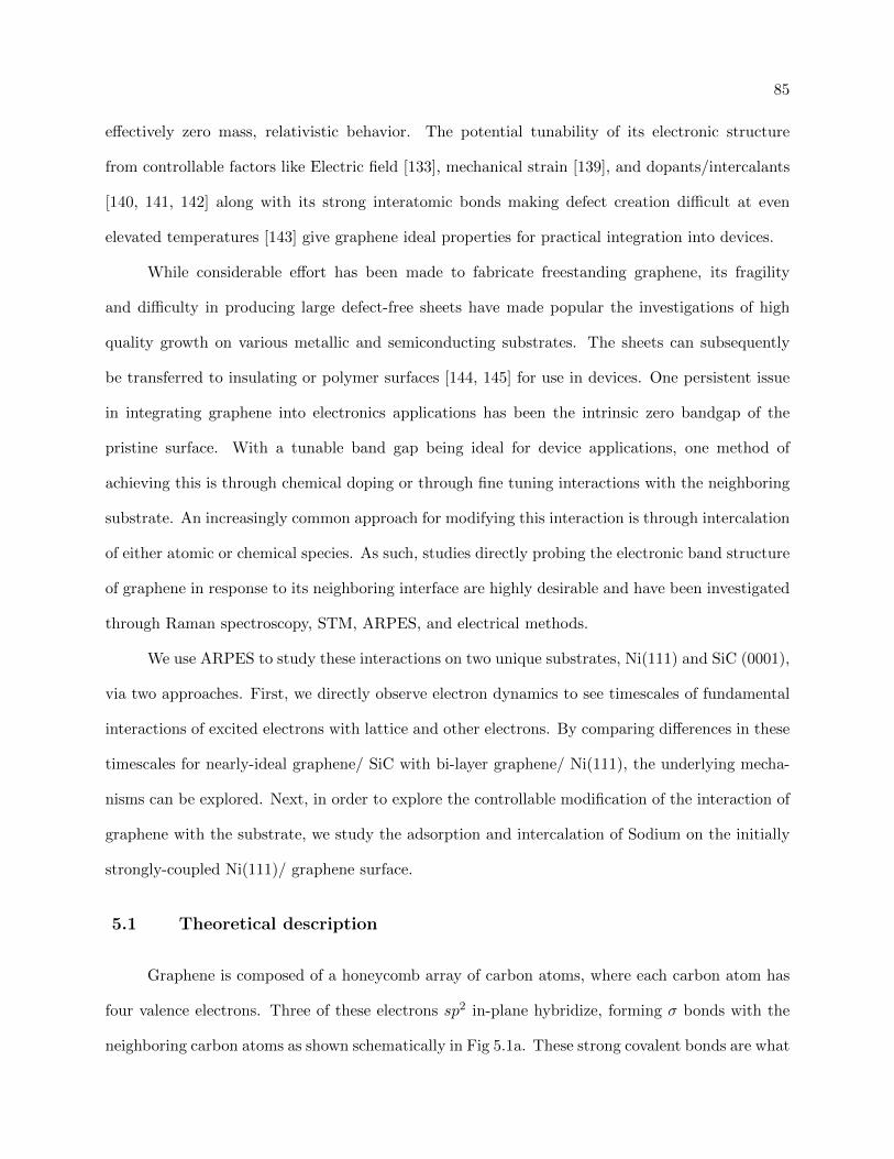
85
effectively zero mass, relativistic behavior. The potential tunability of its electronic structure
from controllable factors like Electric field [133], mechanical strain [139], and dopants/intercalants
[140, 141, 142] along with its strong interatomic bonds making defect creation difficult at even
elevated temperatures [143] give graphene ideal properties for practical integration into devices.
While considerable effort has been made to fabricate freestanding graphene, its fragility
and difficulty in producing large defect-free sheets have made popular the investigations of high
quality growth on various metallic and semiconducting substrates. The sheets can subsequently
be transferred to insulating or polymer surfaces [144, 145] for use in devices. One persistent issue
in integrating graphene into electronics applications has been the intrinsic zero bandgap of the
pristine surface. With a tunable band gap being ideal for device applications, one method of
achieving this is through chemical doping or through fine tuning interactions with the neighboring
substrate. An increasingly common approach for modifying this interaction is through intercalation
of either atomic or chemical species. As such, studies directly probing the electronic band structure
of graphene in response to its neighboring interface are highly desirable and have been investigated
through Raman spectroscopy, STM, ARPES, and electrical methods.
We use ARPES to study these interactions on two unique substrates, Ni(111) and SiC (0001),
via two approaches. First, we directly observe electron dynamics to see timescales of fundamental
interactions of excited electrons with lattice and other electrons. By comparing differences in these
timescales for nearly-ideal graphene/ SiC with bi-layer graphene/ Ni(111), the underlying mecha-
nisms can be explored. Next, in order to explore the controllable modification of the interaction of
graphene with the substrate, we study the adsorption and intercalation of Sodium on the initially
strongly-coupled Ni(111)/ graphene surface.
5.1 Theoretical description
Graphene is composed of a honeycomb array of carbon atoms, where each carbon atom has
four valence electrons. Three of these electrons sp2 in-plane hybridize, forming σ bonds with the
neighboring carbon atoms as shown schematically in Fig 5.1a. These strong covalent bonds are what
86
is responsible for graphene’s exceptional structural stiffness [146]. The remaining out-of-plane pz
electron forms π bonds with neighboring atoms to create delocalized “rings” of π electron orbitals.
The electronic structure of graphene can be reasonably well understood through even a
simplified tight-binding model. Its unit cell is composed of two sublattices, labeled ”A” and ”B” in
Fig 5.1b, where the equivalency of these two sublattices greatly affects it’s resultant band structure.
In reciprocal space, this corresponds to a hexagonal Brillioun zone, shown in gray in Fig 5.1c, with
high symmetry points of Γ,M,K, andK′
points highlighted. Most of the interest in graphene’s
electronic properties centers around studying the K and K′
points, due to its bands crossing the
Fermi level with linear dispersion in these regions, as discussed below.
b1b2 M
KK’
Γ
b c
Real space k space
BAa2 a1
a
Figure 5.1: (a) representative orbital structure for C-C bonding, from [147] (b) real space latticewith A and B sublattices modeled via lattice vectors labeled as a1 and a2. Unit cell is outlined inyellow. (c) reciprocal space lattice with Brillioun Zone shown in gray.
The energy band structure taking into account the possibility for different symmetries on
sublattices A and B can be found through solving the energy Eigenvalue equation
H(k)c(k) = E(k)S(k)c(k) (5.1)
where E(k) and c(k) denote the eigenvalues and eigen-wavefunctions, respectively. For the π band
that we are primarily interested in for our studies, H(k) can be represented, taking into account
only nearest neighbor interactions, as:
H(k) =
∆/2 −γ0f(k)
−γ0f∗(k) −∆/2
(5.2)
87
where
f(k) = eikya/√
3 + 2cos(kxa/2)e−ikya/2√
3 (5.3)
with ∆ describing the asymmetry between the A and B sublattices (opening a band gap |∆|) and γ0
is the nearest neighbor hopping interaction that can be described by the Fermi velocity according to
v = (√
3/2)aγ0/~, with a being the lattice constant [148, 149]. The overlap integral S(k) accounts
for any nonorthogonality of π orbitals on neighboring sites and is given by:
S(k) =
1 s0f(k)
s0f∗(k) 1
(5.4)
where s0 describes the nonorthogonality of the orbitals. The secular equation det(H − ES) = 0
can then be solved to determine the energy eigenvalues, and the band structure E(k):
det
∆/2− E −(γ0 + Es0)f(k)
−(γ0 + Es0)f∗(k) −∆/2− E
= 0
−∆2
4+ E2 − |f(k)|2[E2s2
0 + 2Es0γ0 + γ20 ] = 0
E(k) =±2|f(k)|2s0γ0 −
[∆2(1− |f(k)|2s2
0) + 4|f(k)|2γ20)]1/2
2(1 + |f(k)|2s20)
(5.5)
Where the plus and minus sign correspond to the π* and π states, respectively. While in a
slightly complicated form, we can study details of Eq. 5.5 for both ideal and “non-ideal” graphene.
For the ideal graphene case, the A and B sublattices are symmetric and ∆ = 0 with s0 << 1.
This results in an energy dispersion of E(k) = ±γ0|f(k)| for the π and π* state, as plotted as a
function of kx and ky in Fig 5.2a. The Fermi level is seen to intersect the bands at singular points
at the K and K′
points, as shown with the red plane, leaving an unfilled antibonding π* state.
In the vicinity of these K points, the energy dispersion can be approximated as E(q) = ±~v|q|
where q is the small momentum vector measured relative to each K point. This gives a linear
dispersion around the K points (lineout shown in Fig 5.2b) that is analogous to the relativistic
dispersion E = ±√
(m2c4 + c2p2) with vanishing effective mass and the Fermi velocity (∼ 1 ∗ 106
m/s) replacing c. Charge carriers within graphene (both electrons and holes) therefore behave like
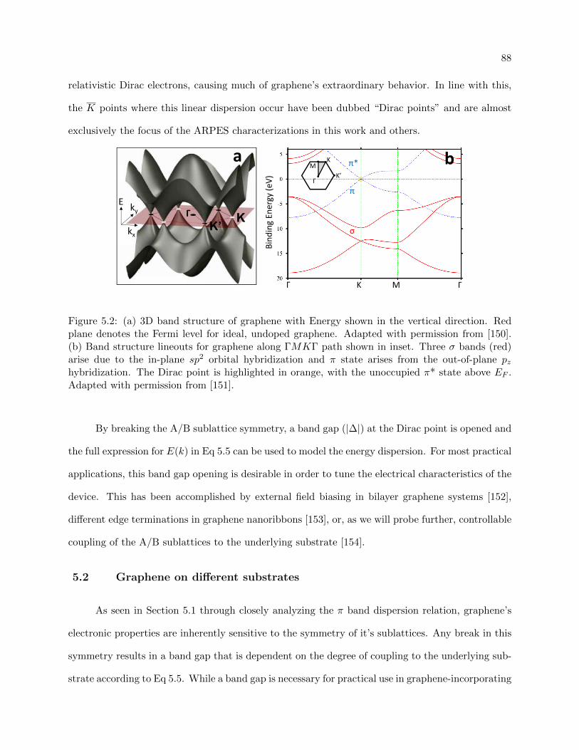
88
relativistic Dirac electrons, causing much of graphene’s extraordinary behavior. In line with this,
the K points where this linear dispersion occur have been dubbed “Dirac points” and are almost
exclusively the focus of the ARPES characterizations in this work and others.
ΓE ky
kx
a
Γ ΓMK
Bind
ing Energy (e
V) Γ
MK
K’
π
σ
π* b
Figure 5.2: (a) 3D band structure of graphene with Energy shown in the vertical direction. Redplane denotes the Fermi level for ideal, undoped graphene. Adapted with permission from [150].(b) Band structure lineouts for graphene along ΓMKΓ path shown in inset. Three σ bands (red)arise due to the in-plane sp2 orbital hybridization and π state arises from the out-of-plane pzhybridization. The Dirac point is highlighted in orange, with the unoccupied π* state above EF .Adapted with permission from [151].
By breaking the A/B sublattice symmetry, a band gap (|∆|) at the Dirac point is opened and
the full expression for E(k) in Eq 5.5 can be used to model the energy dispersion. For most practical
applications, this band gap opening is desirable in order to tune the electrical characteristics of the
device. This has been accomplished by external field biasing in bilayer graphene systems [152],
different edge terminations in graphene nanoribbons [153], or, as we will probe further, controllable
coupling of the A/B sublattices to the underlying substrate [154].
5.2 Graphene on different substrates
As seen in Section 5.1 through closely analyzing the π band dispersion relation, graphene’s
electronic properties are inherently sensitive to the symmetry of it’s sublattices. Any break in this
symmetry results in a band gap that is dependent on the degree of coupling to the underlying sub-
strate according to Eq 5.5. While a band gap is necessary for practical use in graphene-incorporating
89
devices like transistors, this coupling not only needs to be well understood, but highly controllable
for a well behaved device. Several growth methods for graphene are currently being investigated,
with each substrate choice having a varying degree of coupling with its graphene overlayers and
resulting in a wide range of electronic behavior. In graphene production, there is a definite tradeoff
in the degree of this substrate interaction and ease of sample growth. The most common of these
methods are presented here.
Mechanical and Chemical exfoliation: One method for the formation of graphene sheets
has been physical or chemical exfoliation of bulk graphite. Physical exfoliation, or the so called
“scotch tape” technique, usually results in a range of film thicknesses, requiring extra testing to
weed out single layer flakes from multilayer ones [155]. Chemical exfoliation, through solution
phase, has shown promise for large area wafers [156] but are traditionally defect riddled due to
the necessary chemical surface treatments. Only recent work has begun to demonstrate low-defect
large area sheets [157] that might make this method more promising for future work.
SiC Substrates: One of the most prominent methods of graphene growth is an epitaxial
method whereby a SiC substrate is annealed at high temperatures (> 1150C). This results in the
sublimation of the surface silicon and leaves carbon atoms in a well ordered multilayer graphitic
structure on the surface. This procedure yields a slightly different graphene structure when done
on either the C-face or Si-faces of the SiC but with very little electronic coupling to the substrate
itself [135]. Large area, relatively defect-free growth [158, 159] as well as the ability for subsequent
patterning using standard lithographic techniques [160] make this method attractive in achieving
graphene (and graphene ribbons) with precisely tuned electrical characteristics [161]. Due to the
insulating nature of the SiC substrates, subsequent transfer of the graphene to another substrate,
often introducing defects and tears, is also not necessary. However, due to the necessary UHV
and high temperature growth requirements, this may impose practical limitations on integrating
graphene into current production methods.
Metal Substrates: Alternatively, epitaxial graphene growth through catalytic cracking of
hydrocarbons onto transition metal (TM) surfaces has been seen to readily yield large area (> 3
90
inch wafer), low defect sheets [145, 144]. The most common of these substrates investigated have
been Ni(111)[162], Ir(111) [163], Pt(111) [164], Cu [165], and Ru(0001) [139]. However, this growth
scheme has two dominant issues that have been the subject of intensive investigation. First, the
metallic nature of the substrate will most likely necessitate transferring the sheets to an insulating
substrate after large-area growth for use in devices [166, 145, 144, 167]. This is complicated by the
second issue, where hybridization between the d-states of the metal and the π state of the graphene
strongly alters the graphene’s electronic structure and makes physical separation of the graphene
layer from the substrate difficult. The weakening of this interaction via either physical or chemical
modification of the graphene/ TM substrate interface has therefore been of great interest and will
the subject of our investigations in Section 5.6.
5.3 Dynamical Investigations
In addition to investigating the static band structure of graphene on various substrates, un-
derstanding graphene’s nonequilibrium carrier dynamics is essential for understanding its potential
transport properties. Nonequilibrium carrier dynamics are governed by carrier-carrier scattering
and interband (between valence/conduction band) /intraband (within same band) carrier-phonon
scattering with acoustic and optical phonons. These have typically been investigated through ul-
trafast optical methods to capture the short timescale carrier-carrier dynamics that occur within
the first 100 fs [168, 169]. In general, the return to equilibrium state electron/hole distributions is
commonly broken into 3 steps after the initial optical excitation that creates a large population of
non-equilibrium carriers [170, 171].
(1) within the first 50 fs, the initial nonthermal carrier population thermalizes, due to domi-
nant electron-electron scattering, to a distribution well characterized by a hot Fermi-Dirac
distribution
(2) intraband carrier-phonon scattering becomes the dominant relaxation mechanism at inter-
mediate times of 0.4-1.7 ps
91
(3) electron-hole recombination dominant from 1- 15 ps until distribution is again in equilibrium
It should be noted that the mechanisms assigned to the timescales above are found to be the
dominant mechanisms and their contribution is likely nonzero at other times (eg. electron/hole
recombination contributing to the intermediate decay time in (2)). Previous investigations with
short temporal resolution are then able to disentangle the timescales of these dominant relaxation
mechanisms, but are divided in their modeling of the populations with either a single or two
[172] Fermi-Dirac distributions that individually model electrons and holes. Recent time-resolved
terahertz measurements have even been able to tune the photoresponse of the excited carriers from
metal to semiconductor-like through electrostatic gating and actively controlling the Fermi level
[173], demonstrating the sensitive nature of the carriers to the electronic distribution. Due to the
inherently indirect probing of these optical measurements, ARPES allows for direct measurement
of electron/hole relaxation and has only recently been used to investigate the dynamics of p-type
[174, 175] and n-type [176] graphene.
5.4 Chapter Organization
In the remaining experimental sections, we investigate two unique graphene behavioral regimes:
a near-ideal/ weakly coupled (SiC substrate) and a strongly coupled (Ni(111) substrate) graphene
system. Section 5.5 characterizes and probes the electron/ hole dynamics of the C-face SiC(0001)/Graphene
system. Section 5.6 then provides a detailed investigation of the Ni(111)/Graphene system, directly
modifying the strong substrate/graphene coupling via intercalation of alkali atoms to recover a near
ideal electronic structure.
5.5 SiC/ Graphene
Graphene forms epitaxially on 4H- or 6H- silicon carbide substrates through Si desorption at
elevated temperatures. It is able to be grown on both the silicon terminated (0001) or carbon termi-
nated (0001) faces, producing notably different behavior in the resultant graphene growth. While
92
the growth on the Si-face is self terminating after 1-2 layers, the C-face has been seen to grow thick
layers from 5-100 layers depending on growth conditions [158], with larger domain sizes measured
for the (0001) vs (0001) termination of 200nm vs 3-100nm, respectively [177]. With Si-termination,
the resultant graphene sheet is well decoupled electronically from the underlying SiC substrate. In
the C-face substrate however, the first layer in the multisheet stacks is a nonconductive “buffer
layer” covalently bonded to the substrate and greatly modifies the resultant band structure [178].
Subsequent graphene layers are then electronically decoupled [135, 179] due to the stacked layers
being rotated 30 or ±2.2 with respect to each other. This maintains graphene’s 2D electronic
structure until ∼ 10 layers, where a more graphite-like behavior is seen [180]. The Si-face graphene
maintains a 30 rotational stacking that only weakly interacts with the underlying substrate via
Van der Waals forces [181]. Work has been done similar to our alkali intercalation studies in Section
5.6 to try to modify the buffer layer/substrate coupling in (0001) samples through oxygen [182] or
hydrogen [183] intercalation. However, in our following dynamical studies on SiC/ graphene, only
pristine surfaces were probed without modification to the degree of substrate coupling.
5.5.1 Sample Preparation
Si-terminated and C-terminated graphene were prepared ex-situ on 4H-SiC(0001) substrates
according to [177]. Following an acetone/ethanol surface clean, a high temperature ( > 1500 C)
forming gas (95% Ar/ 5% H2) anneal hydrogen etched the surface to produce a well-ordered,
scratch-free surface. Prolonged high temperature heating ( > 1500 C) in a vacuum environment
then produced either 1-2 graphene layers for Si-terminated and 5-6 graphene layers for C-terminated
through Si evaporation.
Samples were flashed to 1000 C via e-beam heating upon insertion into UHV to remove resid-
ual surface adsorbed contaminants like oxygen, water, and hydrocarbons. Noticeable broadening
of the Dirac cone features was seen after roughly 10 hours of measurements due to readsorption of
contaminants. These were removed through subsequent flashes to 1000 C, recovering the original
energy width of the spectral features. Si-face and C-face samples were initially characterized in
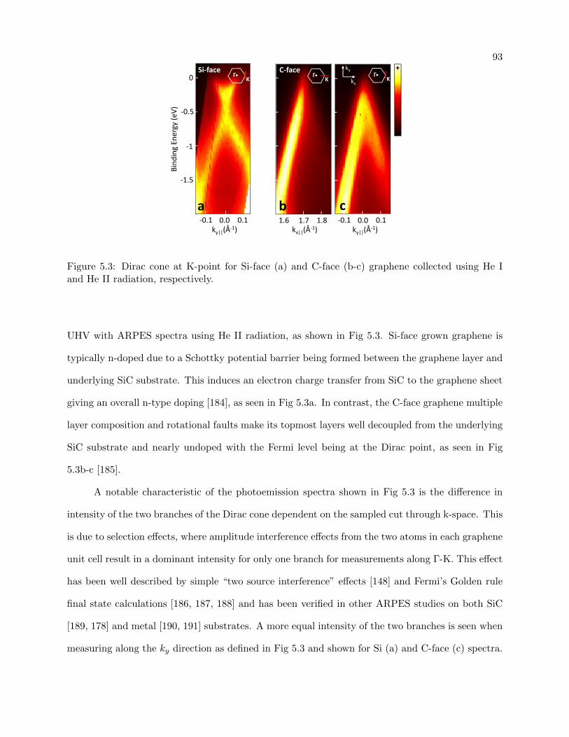
93
1.6 1.7 1.8 ‐0.1 0.0 0.1
C‐faceΓ
KΓ
K
Bind
ing Energy (e
V)
kx||(Å‐1)
b c
0
‐1
‐0.5
‐1.5
Si‐faceΓ
K
aky||(Å‐1) ky||(Å‐1)
kx
ky
‐0.1 0.0 0.1
+
Figure 5.3: Dirac cone at K-point for Si-face (a) and C-face (b-c) graphene collected using He Iand He II radiation, respectively.
UHV with ARPES spectra using He II radiation, as shown in Fig 5.3. Si-face grown graphene is
typically n-doped due to a Schottky potential barrier being formed between the graphene layer and
underlying SiC substrate. This induces an electron charge transfer from SiC to the graphene sheet
giving an overall n-type doping [184], as seen in Fig 5.3a. In contrast, the C-face graphene multiple
layer composition and rotational faults make its topmost layers well decoupled from the underlying
SiC substrate and nearly undoped with the Fermi level being at the Dirac point, as seen in Fig
5.3b-c [185].
A notable characteristic of the photoemission spectra shown in Fig 5.3 is the difference in
intensity of the two branches of the Dirac cone dependent on the sampled cut through k-space. This
is due to selection effects, where amplitude interference effects from the two atoms in each graphene
unit cell result in a dominant intensity for only one branch for measurements along Γ-K. This effect
has been well described by simple “two source interference” effects [148] and Fermi’s Golden rule
final state calculations [186, 187, 188] and has been verified in other ARPES studies on both SiC
[189, 178] and metal [190, 191] substrates. A more equal intensity of the two branches is seen when
measuring along the ky direction as defined in Fig 5.3 and shown for Si (a) and C-face (c) spectra.
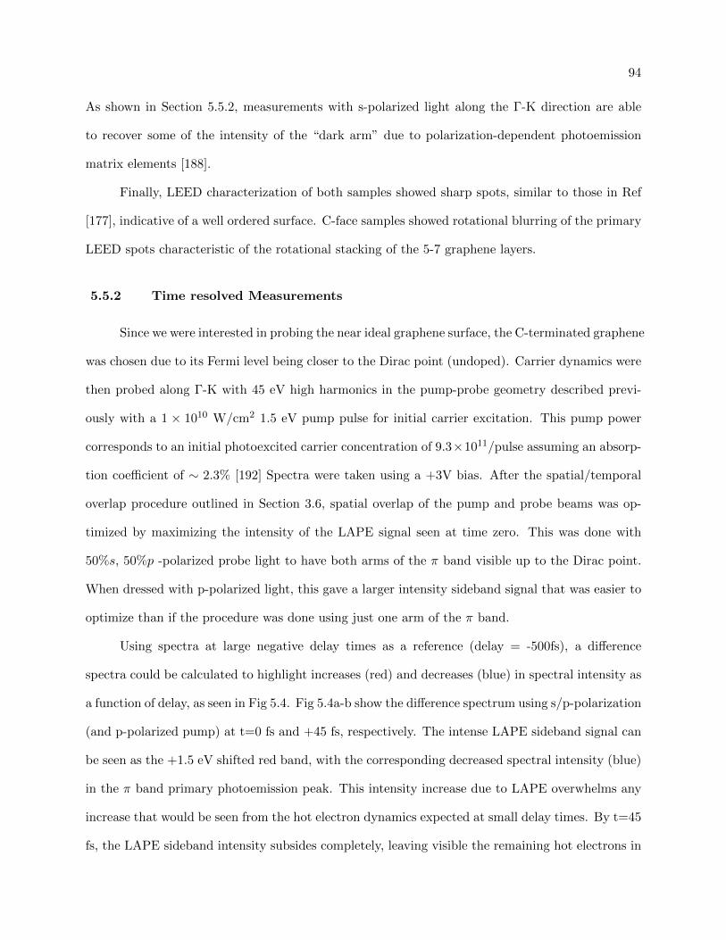
94
As shown in Section 5.5.2, measurements with s-polarized light along the Γ-K direction are able
to recover some of the intensity of the “dark arm” due to polarization-dependent photoemission
matrix elements [188].
Finally, LEED characterization of both samples showed sharp spots, similar to those in Ref
[177], indicative of a well ordered surface. C-face samples showed rotational blurring of the primary
LEED spots characteristic of the rotational stacking of the 5-7 graphene layers.
5.5.2 Time resolved Measurements
Since we were interested in probing the near ideal graphene surface, the C-terminated graphene
was chosen due to its Fermi level being closer to the Dirac point (undoped). Carrier dynamics were
then probed along Γ-K with 45 eV high harmonics in the pump-probe geometry described previ-
ously with a 1 × 10¹⁰ W/cm2 1.5 eV pump pulse for initial carrier excitation. This pump power
corresponds to an initial photoexcited carrier concentration of 9.3×10¹¹/pulse assuming an absorp-
tion coefficient of ∼ 2.3% [192] Spectra were taken using a +3V bias. After the spatial/temporal
overlap procedure outlined in Section 3.6, spatial overlap of the pump and probe beams was op-
timized by maximizing the intensity of the LAPE signal seen at time zero. This was done with
50%s, 50%p -polarized probe light to have both arms of the π band visible up to the Dirac point.
When dressed with p-polarized light, this gave a larger intensity sideband signal that was easier to
optimize than if the procedure was done using just one arm of the π band.
Using spectra at large negative delay times as a reference (delay = -500fs), a difference
spectra could be calculated to highlight increases (red) and decreases (blue) in spectral intensity as
a function of delay, as seen in Fig 5.4. Fig 5.4a-b show the difference spectrum using s/p-polarization
(and p-polarized pump) at t=0 fs and +45 fs, respectively. The intense LAPE sideband signal can
be seen as the +1.5 eV shifted red band, with the corresponding decreased spectral intensity (blue)
in the π band primary photoemission peak. This intensity increase due to LAPE overwhelms any
increase that would be seen from the hot electron dynamics expected at small delay times. By t=45
fs, the LAPE sideband intensity subsides completely, leaving visible the remaining hot electrons in
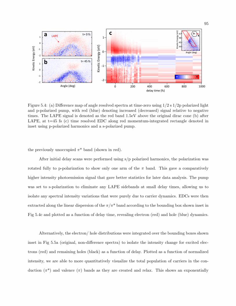
95
2‐21‐2012 Cface #7 (p pol pump, s/p‐pol probe)
Kine
tic Ene
rgy (eV)
1
0
‐1
‐2
0 200 400 600 800 1000delay time (fs)
Angle (deg)
47
46
45
44Kine
tic Ene
rgy (eV)
ΓK
Angle (deg)
Kine
tic Ene
rgy (eV)
‐2
‐1
0
1
‐2
‐1
0
1t= 0 fs
t= 45 fs
LAPEa c
b
+‐
Figure 5.4: (a) Difference map of angle resolved spectra at time-zero using 1/2 s 1/2p polarized lightand p-polarized pump, with red (blue) denoting increased (decreased) signal relative to negativetimes. The LAPE signal is denoted as the red band 1.5eV above the original dirac cone (b) afterLAPE, at t=45 fs (c) time resolved EDC along red momentum-integrated rectangle denoted ininset using p-polarized harmonics and a s-polarized pump.
the previously unoccupied π* band (shown in red).
After initial delay scans were performed using s/p polarized harmonics, the polarization was
rotated fully to p-polarization to show only one arm of the π band. This gave a comparatively
higher intensity photoemission signal that gave better statistics for later data analysis. The pump
was set to s-polarization to eliminate any LAPE sidebands at small delay times, allowing us to
isolate any spectral intensity variations that were purely due to carrier dynamics. EDCs were then
extracted along the linear dispersion of the π/π* band according to the bounding box shown inset in
Fig 5.4c and plotted as a function of delay time, revealing electron (red) and hole (blue) dynamics.
Alternatively, the electron/ hole distributions were integrated over the bounding boxes shown
inset in Fig 5.5a (original, non-difference spectra) to isolate the intensity change for excited elec-
trons (red) and remaining holes (black) as a function of delay. Plotted as a function of normalized
intensity, we are able to more quantitatively visualize the total population of carriers in the con-
duction (π*) and valence (π) bands as they are created and relax. This shows an exponentially
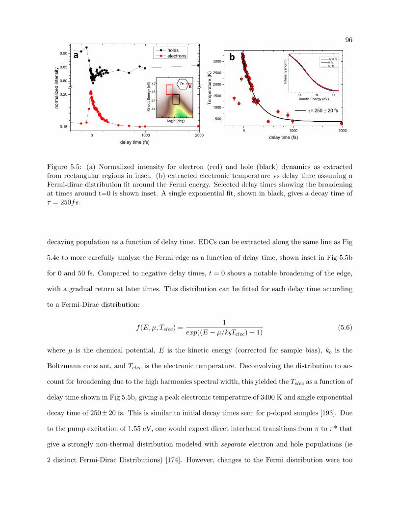
96
0 1000 2000
500
1000
1500
2000
2500
3000
= 250 20 fs
Tem
pera
ture
(K)
delay time (fs)0 1000 2000
0.15
0.20
0.80
0.85
0.90no
rmal
ized
inte
nsity
delay time (fs)
holes electrons
47
46
45
44
Angle (deg)
Kine
tic Ene
rgy (eV) Γ
K
2‐21‐2012 Cface #11 (s pol pump, p‐pol probe)
a b
b) Deconvolving harmonic broadening ‐> fit of single exponential was sufficient. Width of harmonics might have limited resolution of edge
45 46 47
Inte
nsity
(nor
m)
Kinetic Energy (eV)
-500 fs 0 fs 50 fs
Figure 5.5: (a) Normalized intensity for electron (red) and hole (black) dynamics as extractedfrom rectangular regions in inset. (b) extracted electronic temperature vs delay time assuming aFermi-dirac distribution fit around the Fermi energy. Selected delay times showing the broadeningat times around t=0 is shown inset. A single exponential fit, shown in black, gives a decay time ofτ = 250fs.
decaying population as a function of delay time. EDCs can be extracted along the same line as Fig
5.4c to more carefully analyze the Fermi edge as a function of delay time, shown inset in Fig 5.5b
for 0 and 50 fs. Compared to negative delay times, t = 0 shows a notable broadening of the edge,
with a gradual return at later times. This distribution can be fitted for each delay time according
to a Fermi-Dirac distribution:
f(E,µ, Telec) =1
exp((E − µ/kbTelec) + 1)(5.6)
where µ is the chemical potential, E is the kinetic energy (corrected for sample bias), kb is the
Boltzmann constant, and Telec is the electronic temperature. Deconvolving the distribution to ac-
count for broadening due to the high harmonics spectral width, this yielded the Telec as a function of
delay time shown in Fig 5.5b, giving a peak electronic temperature of 3400 K and single exponential
decay time of 250±20 fs. This is similar to initial decay times seen for p-doped samples [193]. Due
to the pump excitation of 1.55 eV, one would expect direct interband transitions from π to π* that
give a strongly non-thermal distribution modeled with separate electron and hole populations (ie
2 distinct Fermi-Dirac Distributions) [174]. However, changes to the Fermi distribution were too
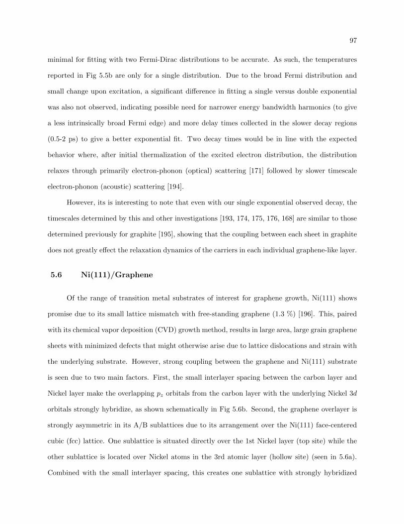
97
minimal for fitting with two Fermi-Dirac distributions to be accurate. As such, the temperatures
reported in Fig 5.5b are only for a single distribution. Due to the broad Fermi distribution and
small change upon excitation, a significant difference in fitting a single versus double exponential
was also not observed, indicating possible need for narrower energy bandwidth harmonics (to give
a less intrinsically broad Fermi edge) and more delay times collected in the slower decay regions
(0.5-2 ps) to give a better exponential fit. Two decay times would be in line with the expected
behavior where, after initial thermalization of the excited electron distribution, the distribution
relaxes through primarily electron-phonon (optical) scattering [171] followed by slower timescale
electron-phonon (acoustic) scattering [194].
However, its is interesting to note that even with our single exponential observed decay, the
timescales determined by this and other investigations [193, 174, 175, 176, 168] are similar to those
determined previously for graphite [195], showing that the coupling between each sheet in graphite
does not greatly effect the relaxation dynamics of the carriers in each individual graphene-like layer.
5.6 Ni(111)/Graphene
Of the range of transition metal substrates of interest for graphene growth, Ni(111) shows
promise due to its small lattice mismatch with free-standing graphene (1.3 %) [196]. This, paired
with its chemical vapor deposition (CVD) growth method, results in large area, large grain graphene
sheets with minimized defects that might otherwise arise due to lattice dislocations and strain with
the underlying substrate. However, strong coupling between the graphene and Ni(111) substrate
is seen due to two main factors. First, the small interlayer spacing between the carbon layer and
Nickel layer make the overlapping pz orbitals from the carbon layer with the underlying Nickel 3d
orbitals strongly hybridize, as shown schematically in Fig 5.6b. Second, the graphene overlayer is
strongly asymmetric in its A/B sublattices due to its arrangement over the Ni(111) face-centered
cubic (fcc) lattice. One sublattice is situated directly over the 1st Nickel layer (top site) while the
other sublattice is located over Nickel atoms in the 3rd atomic layer (hollow site) (seen in 5.6a).
Combined with the small interlayer spacing, this creates one sublattice with strongly hybridized
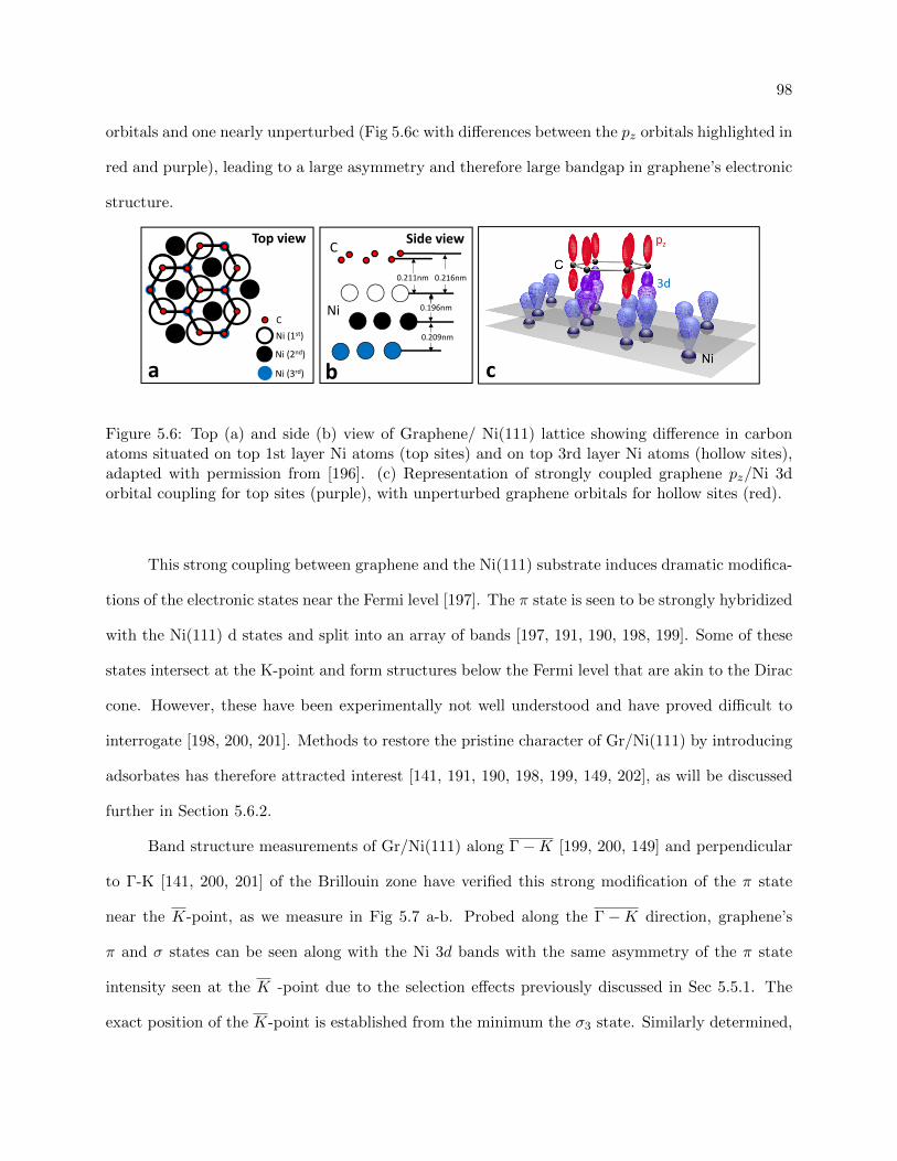
98
orbitals and one nearly unperturbed (Fig 5.6c with differences between the pz orbitals highlighted in
red and purple), leading to a large asymmetry and therefore large bandgap in graphene’s electronic
structure.
b ca
CNi (1st)
Ni (2nd)
Ni (3rd)
Ni
CTop view Side view
0.211nm 0.216nm
0.196nm
0.209nm
pz
3d
Figure 5.6: Top (a) and side (b) view of Graphene/ Ni(111) lattice showing difference in carbonatoms situated on top 1st layer Ni atoms (top sites) and on top 3rd layer Ni atoms (hollow sites),adapted with permission from [196]. (c) Representation of strongly coupled graphene pz/Ni 3dorbital coupling for top sites (purple), with unperturbed graphene orbitals for hollow sites (red).
This strong coupling between graphene and the Ni(111) substrate induces dramatic modifica-
tions of the electronic states near the Fermi level [197]. The π state is seen to be strongly hybridized
with the Ni(111) d states and split into an array of bands [197, 191, 190, 198, 199]. Some of these
states intersect at the K-point and form structures below the Fermi level that are akin to the Dirac
cone. However, these have been experimentally not well understood and have proved difficult to
interrogate [198, 200, 201]. Methods to restore the pristine character of Gr/Ni(111) by introducing
adsorbates has therefore attracted interest [141, 191, 190, 198, 199, 149, 202], as will be discussed
further in Section 5.6.2.
Band structure measurements of Gr/Ni(111) along Γ−K [199, 200, 149] and perpendicular
to Γ-K [141, 200, 201] of the Brillouin zone have verified this strong modification of the π state
near the K-point, as we measure in Fig 5.7 a-b. Probed along the Γ−K direction, graphene’s
π and σ states can be seen along with the Ni 3d bands with the same asymmetry of the π state
intensity seen at the K -point due to the selection effects previously discussed in Sec 5.5.1. The
exact position of the K-point is established from the minimum the σ3 state. Similarly determined,
99
Binding Energy (eV)
Bind
ing Energy (e
V)
σ3
σ2
K
3d
π
b
a
0‐4‐8‐12
Momentum k||(Å‐1)
Bind
ing Energy (e
V)
cΓ
K
Figure 5.7: (a) Experimental collected ARPES spectrum of Gr/Ni(111) near the K point, takenalong Γ-K as shown in the expanded panel. The hybridization of the π state near the K-pointis shown in the expanded panel, with the vertical dashed line indicating the K-point (establishedfrom the minimum of graphene’s σ3 state). The manifold of states arising from Ni 3d and grapheneπ state hybridization is indicated with the bracket. (b) corresponding EDC lineouts of (a) as afunction of momenta (vertical) with graphene states noted. The EDC lineout at the K-point isindicated in red. The weak feature near the Fermi level is a hybridized state in panel (c) shown inred. (c) DFT calculated majority states near the K-point, with graphene 2pz states highlighted inred.
the exact position of the Γ point can be determined from the minimum of the π band. In the
expanded panel around the K-point, the π state maximum is seen to be roughly 2.8 eV below the
Fermi edge then for graphene on SiC(0001), pointing to hybridization between the Ni d band and
graphene π state upon these states intersecting [197, 149]. This collection of hybridized states near
the Fermi level is indicated with the bracket. In support of this, the dispersion of the π state is
seen to be notably lower in the momentum range from 1.5 A−1
to 1.7 A−1
. This is due to π state
coupling to the Ni states, which is strong in the corresponding momentum range down to -3 eV. Fig
100
5.7b shows the corresponding EDCs for the raw ARPES spectra in (a) to highlight the maximum in
the π band seen at -2.8 eV. Also indicated is a subtle π hybridized band (in dashed black) directly
below the Fermi level, and noted in the expanded panel of Fig 5.7a.
To gain further insights into the Gr π/ Ni 3d state coupling, DFT calculations were performed
assuming the stacking configuration in Fig 5.6a. Shown in Fig 5.7c, the d band and the π state are
notably mixed and split into a dense manifold of states for energies down to -3 eV. States relevant to
the 2pz state of graphene are shown in red. It should be noted that these calculations omit spectral
weights or matrix elements effects seen in ARPES, making it possible to show all relevant states
along Γ−K. Our experimental spectrum in Fig 5.7a-b, however, is dominated by the strongest
spectral features. The intensity of the majority of these hybridized states is low measured along
Γ−K due to matrix element effects, which are induced by hybridization [203, 204, 200]. These
states have been previously characterized using higher energy photons and/or other cuts through
the Brillouin zone [200, 201] and are not important for the intercalation studies presented in Section
5.6.2.
Lastly, due a lower density of Ni(111) states at the K point around the Fermi level, the extent
of the π state hybridization with the Ni d bands is notably lower. As such, the remnants of the
π state near the Fermi level can be identified, as denoted with the red arrow. This corresponds
well with the subtle π hybridized band identified in Fig 5.7a-b, showing excellent agreement of
calculated spectra with experiment.
5.6.1 Sample Preparation
The Ni(111) substrates were initially prepared by sputtering 500 nm of nickel onto α-Al2O3(0001)
substrates, as described in reference [205]. Substrates were then transferred into the UHV chamber
and cleaned by cycles of annealing at a temperature of 1100 K, followed by mild sputtering at an
elevated temperature of 1100 K and at a beam-energy of 1 keV. LEED measurements exhibited a
clear (111) nickel structure, as shown in Fig. 5.8a. Magnetic force microscopy (MFM) characteri-
zations, shown in Fig. 5.8b, demonstrated clear “worm-like” magnetic domains out of plane with
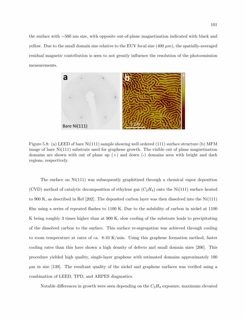
101
the surface with ∼500 nm size, with opposite out-of-plane magnetization indicated with black and
yellow. Due to the small domain size relative to the EUV focal size (400 µm), the spatially-averaged
residual magnetic contribution is seen to not greatly influence the resolution of the photoemission
measurements.
5 µm‐
+
0 50 100 150 200 2502.6
2.8
3.0
3.2
3.4
3.6
3.8
4.0
Wor
k Fu
nctio
n (e
V)
Dosing Time (s)
Na/Gr/ Ni(111)
0.0 0.5 1.0 1.5 2.0 2.5Estimated Na coverage (ML)
φNa= 2.7 eV
φGr= 3.9 eV
a b
Bare Ni(111)
Figure 5.8: (a) LEED of bare Ni(111) sample showing well ordered (111) surface structure (b) MFMimage of bare Ni(111) substrate used for graphene growth. The visible out of plane magnetizationdomains are shown with out of plane up (+) and down (-) domains seen with bright and darkregions, respectively.
The surface on Ni(111) was subsequently graphitized through a chemical vapor deposition
(CVD) method of catalytic decomposition of ethylene gas (C2H4) onto the Ni(111) surface heated
to 900 K, as described in Ref [202]. The deposited carbon layer was then dissolved into the Ni(111)
film using a series of repeated flashes to 1100 K. Due to the solubility of carbon in nickel at 1100
K being roughly 3 times higher than at 900 K, slow cooling of the substrate leads to precipitating
of the dissolved carbon to the surface. This surface re-segregation was achieved through cooling
to room temperature at rates of ca. 8-10 K/min. Using this graphene formation method, faster
cooling rates than this have shown a high density of defects and small domain sizes [206]. This
procedure yielded high quality, single-layer graphene with estimated domains approximately 100
µm in size [139]. The resultant quality of the nickel and graphene surfaces was verified using a
combination of LEED, TPD, and ARPES diagnostics.
Notable differences in growth were seen depending on the C2H4 exposure, maximum elevated
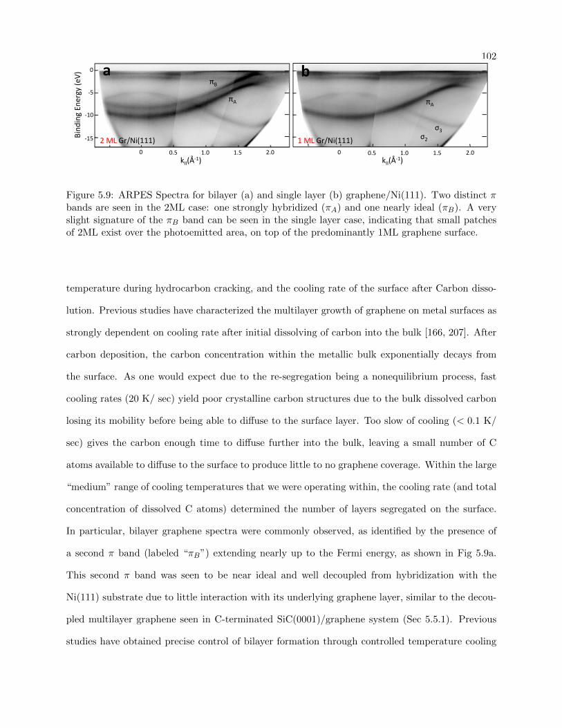
1020
‐5
‐10
‐15
0 0.5 1.0 1.5 2.0 0 0.5 1.0 1.5 2.0
Bind
ing Energy (e
V)
kII(Å‐1) kII(Å‐1)
2 ML Gr/Ni(111) 1 ML Gr/Ni(111)
πA
πB
σ2σ3
πA
a b
Figure 5.9: ARPES Spectra for bilayer (a) and single layer (b) graphene/Ni(111). Two distinct πbands are seen in the 2ML case: one strongly hybridized (πA) and one nearly ideal (πB). A veryslight signature of the πB band can be seen in the single layer case, indicating that small patchesof 2ML exist over the photoemitted area, on top of the predominantly 1ML graphene surface.
temperature during hydrocarbon cracking, and the cooling rate of the surface after Carbon disso-
lution. Previous studies have characterized the multilayer growth of graphene on metal surfaces as
strongly dependent on cooling rate after initial dissolving of carbon into the bulk [166, 207]. After
carbon deposition, the carbon concentration within the metallic bulk exponentially decays from
the surface. As one would expect due to the re-segregation being a nonequilibrium process, fast
cooling rates (20 K/ sec) yield poor crystalline carbon structures due to the bulk dissolved carbon
losing its mobility before being able to diffuse to the surface layer. Too slow of cooling (< 0.1 K/
sec) gives the carbon enough time to diffuse further into the bulk, leaving a small number of C
atoms available to diffuse to the surface to produce little to no graphene coverage. Within the large
“medium” range of cooling temperatures that we were operating within, the cooling rate (and total
concentration of dissolved C atoms) determined the number of layers segregated on the surface.
In particular, bilayer graphene spectra were commonly observed, as identified by the presence of
a second π band (labeled “πB”) extending nearly up to the Fermi energy, as shown in Fig 5.9a.
This second π band was seen to be near ideal and well decoupled from hybridization with the
Ni(111) substrate due to little interaction with its underlying graphene layer, similar to the decou-
pled multilayer graphene seen in C-terminated SiC(0001)/graphene system (Sec 5.5.1). Previous
studies have obtained precise control of bilayer formation through controlled temperature cooling
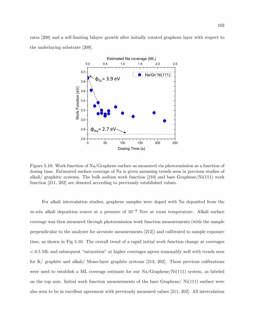
103
rates [208] and a self-limiting bilayer growth after initially rotated graphene layer with respect to
the underlaying substrate [209].
5 µm‐
+
0 50 100 150 200 2502.6
2.8
3.0
3.2
3.4
3.6
3.8
4.0
Wor
k Fu
nctio
n (e
V)
Dosing Time (s)
Na/Gr/ Ni(111)
0.0 0.5 1.0 1.5 2.0 2.5Estimated Na coverage (ML)
φNa= 2.7 eV
φGr= 3.9 eV
Figure 5.10: Work function of Na/Graphene surface as measured via photoemission as a function ofdosing time. Estimated surface coverage of Na is given assuming trends seen in previous studies ofalkali/ graphitic systems. The bulk sodium work function [210] and bare Graphene/Ni(111) workfunction [211, 202] are denoted according to previously established values.
For alkali intercalation studies, graphene samples were doped with Na deposited from the
in-situ alkali deposition source at a pressure of 10−9 Torr at room temperature. Alkali surface
coverage was then measured through photoemission work function measurements (with the sample
perpendicular to the analyzer for accurate measurements [212]) and calibrated to sample exposure
time, as shown in Fig 5.10. The overall trend of a rapid initial work function change at coverages
< 0.5 ML and subsequent “saturation” at higher coverages agrees reasonably well with trends seen
for K/ graphite and alkali/ Mono-layer graphite systems [213, 202]. These previous calibrations
were used to establish a ML coverage estimate for our Na/Graphene/Ni(111) system, as labeled
on the top axis. Initial work function measurements of the bare Graphene/ Ni(111) surface were
also seen to be in excellent agreement with previously measured values [211, 202]. All intercalation
104
studies presented here were performed within the “saturation” regime of ∼ 0.8 ML Na coverage. It
should be noted that no clear LEED superstructure of Na on Graphene was observed for the 0.8ML
dosing either in intercalated or adsorbed studies. This is consistent with previous studies of Cs
intercalation on graphene which only saw superstructures, and therefore well organized crystalline
arrangement, for > 0.9ML or low temperatures [214].
A one hour, low temperature anneal (between 300-400K) was then done to rearrange Na
atoms into a uniform sub-monolayer (in case of non-uniform deposition from the filament source).
No significant desorption of Na or intercalation was observed during this time, as determined from
the unchanging surface work function and oxidation studies (presented below). Intercalation studies
were then performed via ramping the temperature above 400K, using ARPES and the He II photon
source to observe resultant changes in the electronic structure.
5.6.2 Intercalation of Alkali Atoms
Intercalation of noble metals into Graphene has been shown to break down hybridization at
the graphene-metal interface, making it possible to transfer graphene from Ni(111) onto different
substrates for utilization in devices [207]. Physical intercalation of atoms like Au [140], Ag, Cu,
and Fe [137] results in the reduction of coupling to underlying substrate due to increasing the
spacing between the carbon and substrate lattices, resulting in decreased orbital hybridization.
Similarly, the “chemical” intercalation of alkalis [202] is seen to result in a similar decoupling due
to preoccupying the metal substrate orbitals and yielding nearly unperturbed carbon pz orbitals.
The mechanism of decoupling Gr/Ni(111) by intercalation of noble metals is well understood
but, there is little understanding of decoupling by alkali metals [197, 191, 215, 216, 217, 218, 219,
220, 221, 167]. Although intercalated alkali atoms should detach graphene in a similar matter to
noble metals, while also transferring charge and therefore n-doping, studies to date show significant
inconsistency in experimental results. On one hand, intercalation of Na (K and Cs) was shown
to reduce the energy gap between the non-hybridized states at the K-point (the π-to-π* energy
gap) to 1.3 eV [202, 149]. On the other hand, a recent study using angle-resolved photoemission
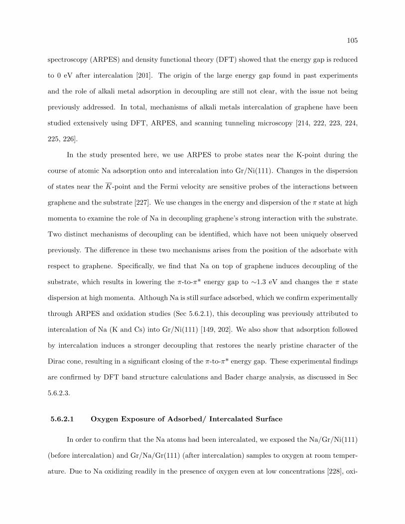
105
spectroscopy (ARPES) and density functional theory (DFT) showed that the energy gap is reduced
to 0 eV after intercalation [201]. The origin of the large energy gap found in past experiments
and the role of alkali metal adsorption in decoupling are still not clear, with the issue not being
previously addressed. In total, mechanisms of alkali metals intercalation of graphene have been
studied extensively using DFT, ARPES, and scanning tunneling microscopy [214, 222, 223, 224,
225, 226].
In the study presented here, we use ARPES to probe states near the K-point during the
course of atomic Na adsorption onto and intercalation into Gr/Ni(111). Changes in the dispersion
of states near the K-point and the Fermi velocity are sensitive probes of the interactions between
graphene and the substrate [227]. We use changes in the energy and dispersion of the π state at high
momenta to examine the role of Na in decoupling graphene’s strong interaction with the substrate.
Two distinct mechanisms of decoupling can be identified, which have not been uniquely observed
previously. The difference in these two mechanisms arises from the position of the adsorbate with
respect to graphene. Specifically, we find that Na on top of graphene induces decoupling of the
substrate, which results in lowering the π-to-π* energy gap to ∼1.3 eV and changes the π state
dispersion at high momenta. Although Na is still surface adsorbed, which we confirm experimentally
through ARPES and oxidation studies (Sec 5.6.2.1), this decoupling was previously attributed to
intercalation of Na (K and Cs) into Gr/Ni(111) [149, 202]. We also show that adsorption followed
by intercalation induces a stronger decoupling that restores the nearly pristine character of the
Dirac cone, resulting in a significant closing of the π-to-π* energy gap. These experimental findings
are confirmed by DFT band structure calculations and Bader charge analysis, as discussed in Sec
5.6.2.3.
5.6.2.1 Oxygen Exposure of Adsorbed/ Intercalated Surface
In order to confirm that the Na atoms had been intercalated, we exposed the Na/Gr/Ni(111)
(before intercalation) and Gr/Na/Gr(111) (after intercalation) samples to oxygen at room temper-
ature. Due to Na oxidizing readily in the presence of oxygen even at low concentrations [228], oxi-
106
0
‐5
‐10
‐15
0
‐5
‐10
‐15
1.3 1.5 1.7 1.3 1.5 1.7
a
b
c
dk||(Å‐1) k||(Å‐1)
Bind
ing Energy (e
V)Na/Gr/Ni(111) Gr/Na/Ni(111)
π
π*
Sodium oxide
σ3σ2
Figure 5.11: (a) Electronic structure of Gr/Ni(111) near the K-point after adsorption and uniformrearrangement 0.8 ML of adsorbate on top, note large band gap of ∼1.3 eV. (b) Same sampleas in (a) after exposure to oxygen at 10−8 Torr for 40 min with visible sodium oxide states (c)Gr/Ni(111) after adsorption and intercalation of 0.8 ML of Na, with reduced band gap. (d) Samesample as in (c) after exposure to oxygen at 10−8 Torr for 40 min, with no significant sodium oxidelines visible (small amount seen due to residual surface adsorbed Na).
dation should occur if the alkali atoms are not “protected” under the layer of graphene. Graphene
has been seen to protect intercalated Fe atoms from oxidation, due to oxygen being unable to
107
penetrate into graphene at room temperature [137, 229].
Samples remained exposed to a flow of oxygen leaked in to maintain a constant chamber
pressure of 10−8 Torr for ca. 40 minutes. ARPES spectra were recorded during this time using He
II radiation. Figure 5.11a shows spectra recorded after adsorbing (and not intercalating) 0.8 ML
of Na on top of Gr/Ni(111). The analyzer pass energy was chosen to allow simultaneous detection
of high and low kinetic energy electrons, from the Fermi level down to the σ2 and σ3 states. The
π* state near the Fermi level and the π-to-π* energy gap of 1.3 eV indicates that the adsorbate
remains on top, as discussed further in Section 5.6.2.2, due to the weak decoupling of the C pz
orbitals with the Ni(111) substrate.
Shown in Fig. 5.11b, two strong spectral features emerge after oxygen exposure, near -6.5 eV
and -10.5 eV. These features are due to sodium oxide valence states [228], indicating that the Na
adsorbate, residing on top of the graphene layer, is oxidized upon O2 exposure. After intercalation
(as shown in Fig. 5.11c), no sodium oxide states are observed. This indicates that the adsorbate
is protected under the graphene layer and is not able to oxidize. A very weak line at ca. -6.5 eV
is visible in Fig. 5.11d that indicates trace amounts of sodium oxides formed from the very small
fraction of remaining surface adsorbed Na atoms. With this oxidation study serving to validate
the existence of two separate configurations of the Na/Gr/Ni(111) system (with the Na either
being intercalated underneath Gr/Ni(111) of adsorbed on the surface), the transition from surface
adsorbed Na to intercalated Na and its corresponding effects on the graphene band structure could
be probed in detail.
5.6.2.2 Intercalation through Thermal Annealing
After initially dosing the clean Gr/Ni(111) surface (Fig 5.12a) with 0.8 ML Na, the π* state
was seen to be populated and shifted to below the Fermi level, as seen in Fig 5.12b. The π state
maximum also moves closer to the Fermi level (indicated with the yellow arrow) from its initialy
maximum of -2.8 eV and the slope is increased around the K-point, with a lowering of the π-to-π*
energy gap to ∼1.3 eV. Since n-doping should neither shift a populated state towards the Fermi
108
level nor change the state dispersion, these changes of the π state after Na adsorption cannot be
explained as simply due to n-doping. Instead, we conclude that this lower energy gap is due to a
lower coupling between graphene and the substrate after adsorption rather than only n-doping of
the original π/π* bands.
After initial adsorption, changes to the band structure could be seen upon Na intercalation
via thermal annealing. The band gap was seen to reduce significantly after complete intercalation,
as seen in Fig 5.12c. Validation that this state corresponds to complete Na intercalation was done
through the oxidation studies presented in Sec. 5.6.2.1. The spectral intensity of the hybridized
states clearly evident in Fig 5.12a is also strongly diminished after adsorption as seen in Fig. 5.12b,
supporting the idea that the extent of Gr π/Ni 3d hybridization is reduced after adsorption. Panels
(b1) and (b2) show spectra during this transition, with the progressively decreasing band gap
attributed to an increasing number of Na atoms being intercalated underneath the graphene layer
with a decreasing fraction still remaining on the surface.
5.6.2.3 DFT calculations and Bader Charge Analysis
In order to gain more insight into the observed graphene decoupling, DFT and Bader charge
analysis studies were performed in collaboration with Manos Mavrikakis’ group at University of
Wisconsin. The specific computational details of this analysis can be found in Appendix A.5.
Compared to the freestanding graphene case (Fig 5.13a), the dispersion of the Gr/Ni(111) π band
near the K-point is not linear (Fig 5.13b and Fig 5.7c shown for larger energy range), in agreement
with the experimental ARPES spectra. The π* state is also seen to be shifted above the Fermi
level, as highlighted in red. Note that the energy window shown in Fig 5.13 was performed around
the Fermi level down to 4 eV BE to more closely study the evolution of the π/π* states upon Na
adsorption and intercalation.
Figures 5.13c and 5.13d show calculated electronic structures of Gr/Ni(111) with Na on top
and intercalated, respectively. The hybridized π* state above the Fermi level and the remnants of
the π state below the Fermi level are shifted down in energy after Na adsorption (Fig 5.13c). Due
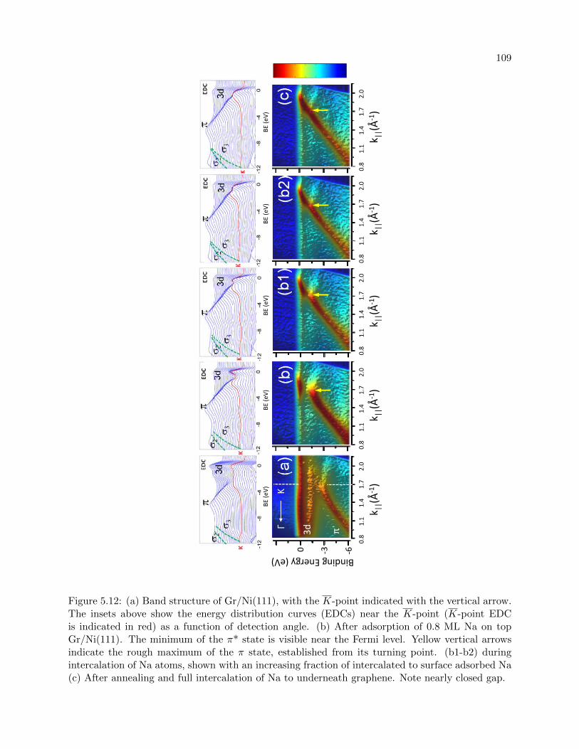
109
Binding Energy (eV)
3d π
KΓ
k ||(Å
‐1)
0.8
1.1
1.4
1.7
2.0
k ||(Å
‐1)
0.8
1.1
1.4
1.7
2.0
k ||(Å
‐1)
0.8
1.1
1.4
1.7
2.0
k ||(Å
‐1)
0.8
1.1
1.4
1.7
2.0
k ||(Å
‐1)
0.8
1.1
1.4
1.7
2.0
0 ‐3 ‐6
BE (e
V)BE
(eV)
BE (e
V)BE
(eV)
BE (e
V)
Figure 5.12: (a) Band structure of Gr/Ni(111), with the K-point indicated with the vertical arrow.The insets above show the energy distribution curves (EDCs) near the K-point (K-point EDCis indicated in red) as a function of detection angle. (b) After adsorption of 0.8 ML Na on topGr/Ni(111). The minimum of the π* state is visible near the Fermi level. Yellow vertical arrowsindicate the rough maximum of the π state, established from its turning point. (b1-b2) duringintercalation of Na atoms, shown with an increasing fraction of intercalated to surface adsorbed Na(c) After annealing and full intercalation of Na to underneath graphene. Note nearly closed gap.
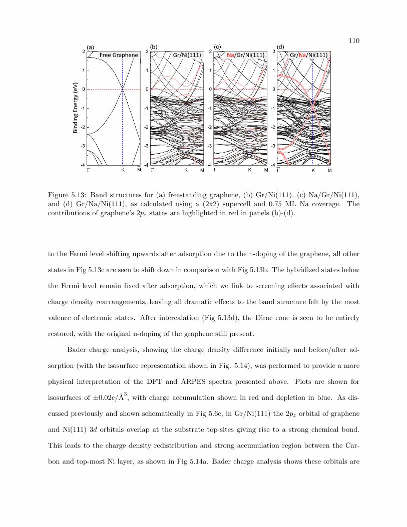
110
Bind
ing Energy (e
V)
Free Graphene Gr/Ni(111) Na/Gr/Ni(111) Gr/Na/Ni(111)
Figure 5.13: Band structures for (a) freestanding graphene, (b) Gr/Ni(111), (c) Na/Gr/Ni(111),and (d) Gr/Na/Ni(111), as calculated using a (2x2) supercell and 0.75 ML Na coverage. Thecontributions of graphene’s 2pz states are highlighted in red in panels (b)-(d).
to the Fermi level shifting upwards after adsorption due to the n-doping of the graphene, all other
states in Fig 5.13c are seen to shift down in comparison with Fig 5.13b. The hybridized states below
the Fermi level remain fixed after adsorption, which we link to screening effects associated with
charge density rearrangements, leaving all dramatic effects to the band structure felt by the most
valence of electronic states. After intercalation (Fig 5.13d), the Dirac cone is seen to be entirely
restored, with the original n-doping of the graphene still present.
Bader charge analysis, showing the charge density difference initially and before/after ad-
sorption (with the isosurface representation shown in Fig. 5.14), was performed to provide a more
physical interpretation of the DFT and ARPES spectra presented above. Plots are shown for
isosurfaces of ±0.02e/A3, with charge accumulation shown in red and depletion in blue. As dis-
cussed previously and shown schematically in Fig 5.6c, in Gr/Ni(111) the 2pz orbital of graphene
and Ni(111) 3d orbitals overlap at the substrate top-sites giving rise to a strong chemical bond.
This leads to the charge density redistribution and strong accumulation region between the Car-
bon and top-most Ni layer, as shown in Fig 5.14a. Bader charge analysis shows these orbitals are
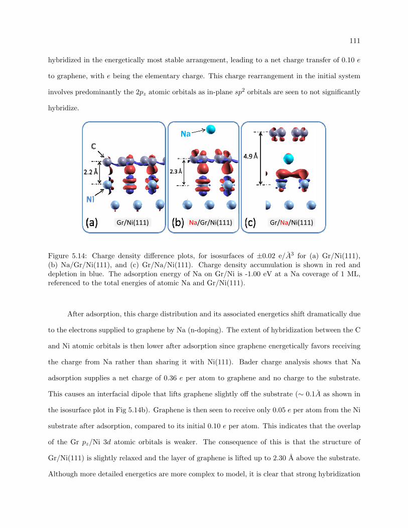
111
hybridized in the energetically most stable arrangement, leading to a net charge transfer of 0.10 e
to graphene, with e being the elementary charge. This charge rearrangement in the initial system
involves predominantly the 2pz atomic orbitals as in-plane sp2 orbitals are seen to not significantly
hybridize.
Gr/Ni(111) Na/Gr/Ni(111) Gr/Na/Ni(111)
Figure 5.14: Charge density difference plots, for isosurfaces of ±0.02 e/A3 for (a) Gr/Ni(111),(b) Na/Gr/Ni(111), and (c) Gr/Na/Ni(111). Charge density accumulation is shown in red anddepletion in blue. The adsorption energy of Na on Gr/Ni is -1.00 eV at a Na coverage of 1 ML,referenced to the total energies of atomic Na and Gr/Ni(111).
After adsorption, this charge distribution and its associated energetics shift dramatically due
to the electrons supplied to graphene by Na (n-doping). The extent of hybridization between the C
and Ni atomic orbitals is then lower after adsorption since graphene energetically favors receiving
the charge from Na rather than sharing it with Ni(111). Bader charge analysis shows that Na
adsorption supplies a net charge of 0.36 e per atom to graphene and no charge to the substrate.
This causes an interfacial dipole that lifts graphene slightly off the substrate (∼ 0.1A as shown in
the isosurface plot in Fig 5.14b). Graphene is then seen to receive only 0.05 e per atom from the Ni
substrate after adsorption, compared to its initial 0.10 e per atom. This indicates that the overlap
of the Gr pz/Ni 3d atomic orbitals is weaker. The consequence of this is that the structure of
Gr/Ni(111) is slightly relaxed and the layer of graphene is lifted up to 2.30 A above the substrate.
Although more detailed energetics are more complex to model, it is clear that strong hybridization
112
is energetically less favorable when graphene is n-doped. Lower electronegativity (and therefore a
higher charge transfer per atom) of adsorbates like K and Cs would yield even stronger decoupling,
consistent with previous measurements on Gr/Ni(111) [202].
Analyzing the corresponding band structure in Fig. 5.13d and the isosurfaces presented in
Fig. 5.14, we see the graphene is lifted up to 4.9 A above the substrate, effectively cutting off
any interaction with the substrate as no bonding can be supported over such a distance. The
hybridization is blocked by an atomic spacer of Na and thus there is no energy gap at the K-point.
The remnant gap opening (5 100 meV) or the minor band back-bending seen in Fig. 5.12(c) is a
result of superposition of regions with complete intercalated Na and regions where Na still remains
on top. This is expected here due to the coverage of Na (0.8 ML) and possibly some bottlenecks
in the intercalation paths.
5.6.3 Discussion and Conclusions
Our ARPES measurements in Sec 5.6.2.2 supported by the DFT calculation and Bader charge
analysis in Sec 5.6.2.3 point to two unique configurations for the Na- Gr/Ni(111) system: surface
adsorbed and intercalated Na. Previous studies, which observed lowering of the π-to-π* energy gap
to 1.3 eV after adsorption of Na (K, Cs) onto Gr/Ni(111) overlooked changes in the dispersion of π
near the K-point [149, 202]. The lowering of the energy gap was attributed to intercalation of Na
(K, Cs) into graphene, although no proof of intercalation was shown. Other studies, under identical
conditions, showed the intercalated ARPES spectrum with no gap at all [201]. By observing the
transition of Na from surface adsorbed to intercalated with the electronic band structure constantly
probed via ARPES, we are able to resolve these inconsistencies.
First, we observe a surface adsorbed Na configuration after deposition. We exclude intercala-
tion as the origin of the band structure changes in Fig 5.12b through the oxidation studies presented
in Sec 5.6.2.1, where O2 exposure of the surface gave rise to photoemission lines from sodium oxides
[228]. We also exclude that this state is due to Na intercalation at isolated areas causing patches
of decoupled and still-coupled graphene since such decoupling has been shown to produce a super-
113
position of two π states, one from intercalated and one from non-intercalated areas [201]. Static
Angle-resolved or angle-integrated X-Ray photoemission spectroscopy (XPS) using high energy
photons to look at photoemission lines from deeply bound core levels has traditionally been used as
a surface-sensitive gauge for coverage of surface adsorbates and overlayers. However, XPS measure-
ments cannot confirm intercalation of Na into graphene since changes in the intensity of XPS lines
from a monolayer of Na (K, Cs) adsorbed on graphene are often due to formation of thick islands of
adsorbates on top rather than intercalation, making XPS intensity differences in the observed core
level states difficult to interpret [223, 229, 230, 137]. We emphasize that this decoupling via surface
adsorption involves notably different mechanisms than decoupling through intercalation of noble
metals into Gr/Ni(111) [141, 190, 198, 201, 215, 216, 223, 229, 230, 231, 232, 233]. In the noble
metal case, bulky atoms break down hybridization at the graphene-substrate interface, resulting in
detaching graphene from the substrate and closing the energy gap between non-hybridized states
at the K-point. When the adsorbate remains on the surface, it changes the energetics and in-
duces relaxation of the bonding at the graphene-substrate interface. However, it does not “detach”
graphene from the substrate by entirely eliminating the orbital hybridization.
Upon intercalation, we find that the energy gap is reduced to ≤ 100 meV and the Dirac cone
is nearly restored. The Fermi velocity, which we can use as a gauge of the coupling to the substrate
[227], is increased after intercalation towards the value of freestanding graphene (∼ 1.6× 10⁶m/s).
Our ARPES experiments and DFT calculations show that intercalation of Na is nearly the same in
its decoupling effectiveness as intercalation of noble metals, although strong n-doping is concurrent
with this decoupling for the case with alkalis.
Although recent experiments have suggested that Na may intercalate spontaneously due to a
low energy barrier [201], we do not observe spontaneous intercalation at room temperature. Instead,
we find that intercalation is not possible unless the graphene layer contains defects or grain bound-
aries and unless the mobility of Na is increased by temperature. Our DFT calculations further
support this observation. Although surface adsorbed Na is not the optimally stable configuration
from the energetics standpoint, with the intercalated configuration being preferable, intercalation
114
is kinetically-limited without grain boundaries and defects. Performing similar intercalation stud-
ies as in Sec 5.6.2.2 on multiple Gr/Ni(111) samples grown under different conditions, we were
able to achieve relatively good control over defect concentration in graphene by introducing oxide
impurities into the Ni(111) substrate. Initiating graphene growth at lower temperatures was seen
to produce impurities of amorphous carbon [196]. Under these conditions, when graphene showed
relatively weak ARPES spectral features and a high background of secondary electrons (indicating
poorer crystal quality resulting in electron scattering), intercalation was possible at lower temper-
atures. Intercalation into a higher quality graphene like that found in Sec 5.6.2.2 required elevated
temperatures, with intercalation into the highest quality graphene needing temperatures close to
the Na desorption threshold. These studies indicate the Na intercalation is highly morphology
dependent.
In summary, we show two distinct configurations of surface adsorption and intercalation for
Na deposited onto Gr/Ni(111). The presence of Na atoms on top of Gr/Ni(111) partially decouples
graphene from the underlying substrate, as evident from a decrease of the π-to-π* energy gap to 1.3
eV, while intercalation recovers the near-pristine graphene, dramatically reducing this energy gap.
The ability to control the extent of this graphene-to-substrate coupling using a charge transfer from
adsorbates, rather than intercalation, opens new possibilities in using optical excitations to control
the electronic state of graphene. This technique might also allow for switching the graphene-to-
substrate coupling in the spirit of previous work with alkali adsorbates on noble metal surfaces
[234, 235, 236]. Potentially, a similar scheme can be applied to other graphene systems making it
useful in novel devices.
Chapter 6
Band bending Studies on InGaAs/high-k/metal Gate Stacks
The revolutionary progress in the complementary metal-oxide-semiconductor (CMOS) inte-
grated circuit (IC) industry over the last 40 years can largely be attributed to the industry’s ability
to satisfy three primary demands: high switching speed, low static power consumption, and a range
of power, output and voltages in the device. [237, 238] The push for increased chip performance at
a low cost has meant an increasingly larger density of devices on a printed IC wafer, with added
benefits to performance as device size is scaled down [239]. This continued miniaturization of de-
vices has kept a consistent pace of quadrupling the number of components on a chip every 3 years.
From 1970 to 2010, the number of transistors per mm2 on a high-production processor increased
from 200 to over 1 million, the progress of which is shown in Fig 6.1 (right) [240]. The workhorse of
this Ultra-Large Scale Integration (ULSI) IC industry has been the metal-oxide-semiconductor field
effect transistor (MOSFET), serving as the basic “switch” component for more intricate circuits
(a general illustration of which is shown Fig 6.1 (left)). The on/off capability of the device, mean-
ing the number of mobile charge carriers in the conducting channel, is tuned through capacitive
coupling (hence the “field effect”) comprised of a metal gate, insulating oxide, and semiconducting
bulk (enlarged inset) and is controlled by the voltage applied to the metal gate of the device. For
a more general discussion of MOSFETs, the reader is referred to Ref. [241].
Thus far, the ability to scale these devices has been facilitated by the inherent beauty of
the Si/SiO2 system. Using doped Silicon as the semiconducting substrate, a native large-scale,
defect-free SiO2 layer is readily grown with a resistivity > 1016 Ωcm [242]. This near perfect
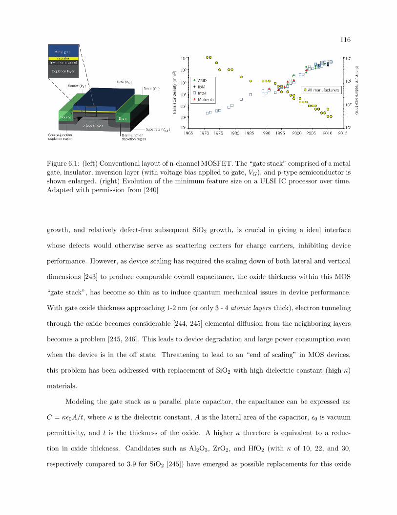
116
Figure 6.1: (left) Conventional layout of n-channel MOSFET. The “gate stack” comprised of a metalgate, insulator, inversion layer (with voltage bias applied to gate, VG), and p-type semiconductor isshown enlarged. (right) Evolution of the minimum feature size on a ULSI IC processor over time.Adapted with permission from [240]
growth, and relatively defect-free subsequent SiO2 growth, is crucial in giving a ideal interface
whose defects would otherwise serve as scattering centers for charge carriers, inhibiting device
performance. However, as device scaling has required the scaling down of both lateral and vertical
dimensions [243] to produce comparable overall capacitance, the oxide thickness within this MOS
“gate stack”, has become so thin as to induce quantum mechanical issues in device performance.
With gate oxide thickness approaching 1-2 nm (or only 3 - 4 atomic layers thick), electron tunneling
through the oxide becomes considerable [244, 245] elemental diffusion from the neighboring layers
becomes a problem [245, 246]. This leads to device degradation and large power consumption even
when the device is in the off state. Threatening to lead to an “end of scaling” in MOS devices,
this problem has been addressed with replacement of SiO2 with high dielectric constant (high-κ)
materials.
Modeling the gate stack as a parallel plate capacitor, the capacitance can be expressed as:
C = κε0A/t, where κ is the dielectric constant, A is the lateral area of the capacitor, ε0 is vacuum
permittivity, and t is the thickness of the oxide. A higher κ therefore is equivalent to a reduc-
tion in oxide thickness. Candidates such as Al2O3, ZrO2, and HfO2 (with κ of 10, 22, and 30,
respectively compared to 3.9 for SiO2 [245]) have emerged as possible replacements for this oxide
117
layer. Performance-inhibiting integration challenges with high-κ oxides, such as charge trapping at
the high-κ/ semiconductor interface due to poor interface quality and fixed charge sites within the
oxide [247, 30] have been successfully addressed through judicious material choice and processing
techniques, and have now been integrated into commercial products.
Of increasing interest has been the replacement of the doped-Silicon semiconducting “base”
with a higher electron mobility material, leading to higher injection current into the channel and
faster device switching. III-V materials (formed from group III & V in the periodic table) have
already been widely implemented in devices like bipolar transistors and photodetectors. These
materials offer an improved electron mobility ten times that of silicon. It should be noted that its
hole mobility is relatively low compared to other materials like Germanium, which have been greatly
explored for use in pFET devices. However, incorporation of these materials, like In0.53Ga0.47As,
has presented additional challenges when paired with high-κ oxides, with a defect-free III-V/high-κ
interface being difficult to achieve due to oxide reformation during deposition [248] and a lower
thermal processing budget needed to minimize elemental diffusion from the III-V material [249].
Trapped charge within the oxide, be it at the interface (border traps) or within the bulk (bulk
traps), can greatly influence the overall performance and reliability of the resultant devices due
to (1) it changing the electronic bands of the semiconductor (2) it acting as scattering centers for
charge carriers and (3) the addition of electronic states within the band gap of the semiconductor
that can serve as energetic traps for carriers.
Multiple techniques including the addition of interfacial layers between the III-V and high-κ
[250, 251], activated plasma cleaning of the III-V surface [252, 253, 254], and forming gas anneal-
ing [255] have been employed to minimize these charge defects, generally being characterized by
electrical measurements (C-V, I-V) of a resultant MOS capacitor (MOScap). While this character-
ization method (discussed in Section 6.1.2) is sensitive in detecting the overall density of interface
charge traps (Dit) within the stack, it fails to capture how and when these defects form. Due to
the high-temperature processing required to pattern these samples, it is inherently unable to probe
the evolution of charge defects at subsequent stages of processing that would otherwise give insight
118
into its driving mechanisms. Additionally, this method becomes problematic in studying systems
with large defect density, as may be the case with III-V systems.
In the following study, we investigate this overall charge state through directly probing the
band bending at the InGaAs/high-κ interface. By employing a pump-probe photoelectron spec-
troscopy technique similar to those discussed in previous studies, we first probe changes in band
bending at subsequent layer depositions to build the full InGaAs/high-κ/TiN stack. To simulate the
effect of thermal processing, annealing studies were performed on InGaAs/high-κ and InGaAs/high-
κ/TiN wafers to probe the change in the net charge state as one approaches the high temperatures
required of device production. In this manner, insight into the creation and changes in the overall
number of charged defects within the stack can be probed. The effect of a forming gas anneal
was then studied on the TiN gated stacks to fully reproduce processing conditions. Band bending
extracted from PES measurements were then directly compared to the Vfb from conventional C-V
electrical measurements on an identical set of wafers subject to full MOScap patterning.
6.1 Technical Background
Unlike the bulk systems presented previously in this work, semiconductor multilayer system
present several unique attributes in their electronic structure that are crucial in understanding the
following studies. In an ideal MOS stack, energy bands of the semiconductor are bent down (p-
type) or up (n-type) in response to the net dipole created due to (1) charge transfer from the metal
into the semiconductor via Schottky transfer of electrons from dissimilar vacuum work functions
(Φmetal 6= Φsemi) and (2) the presence of trapped charges within and at the interface of the oxide.
Shown in Fig 6.2 for a p-type semiconductor, these conduction (EC) and valence (EV ) bands
can be flattened using an applied external voltage to modify the EF of the metal and modifying
the overall dipole (blue arrow) within the stack. As depicted, these bands can also be further
bent from depletion into inversion (red) with a bias of opposite sign. When the intrinsic level
(EI) crosses EF , this opens a channel for minority carriers within the material (thus being able to
conduct the majority carrier between the source and drain in a MOSFET). Through determining
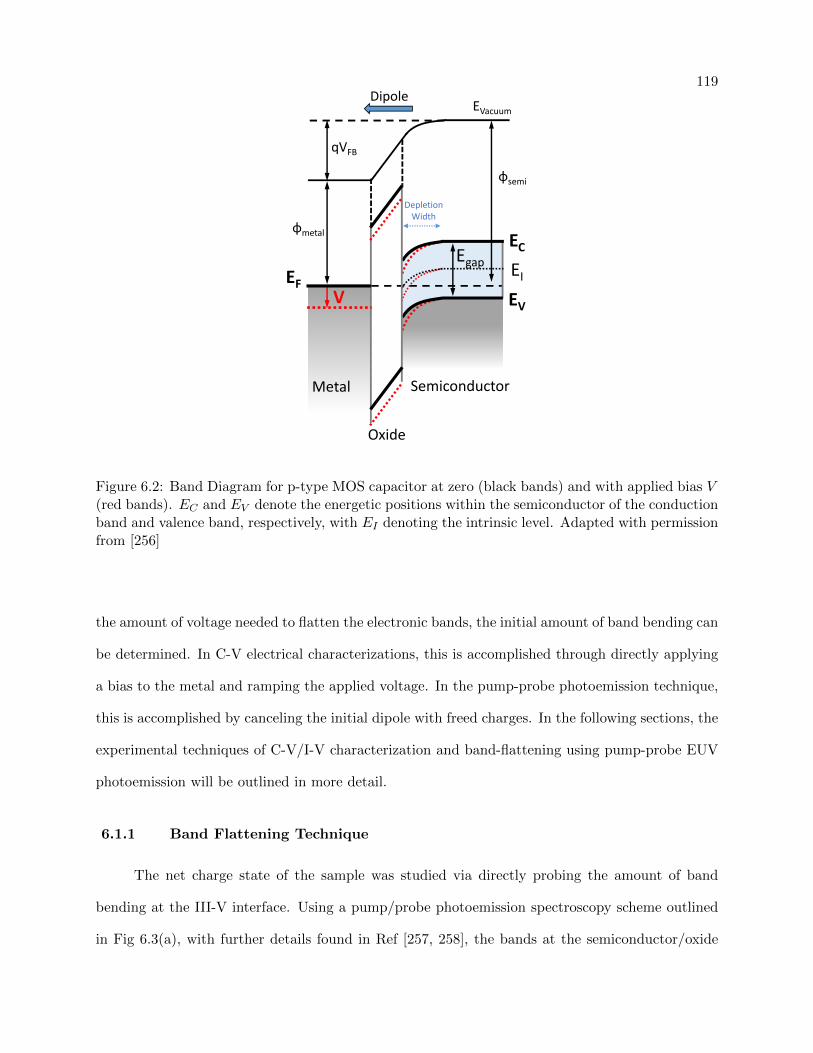
119
φmetal
φsemi
EC
EVEF
qVFB
EVacuum
Metal
Oxide
Semiconductor
EIV
Egap
Dipole
DepletionWidth
Figure 6.2: Band Diagram for p-type MOS capacitor at zero (black bands) and with applied bias V(red bands). EC and EV denote the energetic positions within the semiconductor of the conductionband and valence band, respectively, with EI denoting the intrinsic level. Adapted with permissionfrom [256]
the amount of voltage needed to flatten the electronic bands, the initial amount of band bending can
be determined. In C-V electrical characterizations, this is accomplished through directly applying
a bias to the metal and ramping the applied voltage. In the pump-probe photoemission technique,
this is accomplished by canceling the initial dipole with freed charges. In the following sections, the
experimental techniques of C-V/I-V characterization and band-flattening using pump-probe EUV
photoemission will be outlined in more detail.
6.1.1 Band Flattening Technique
The net charge state of the sample was studied via directly probing the amount of band
bending at the III-V interface. Using a pump/probe photoemission spectroscopy scheme outlined
in Fig 6.3(a), with further details found in Ref [257, 258], the bands at the semiconductor/oxide
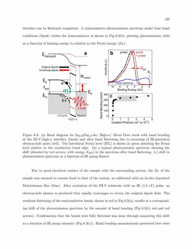
120
interface can be flattened completely. A representative photoemission spectrum under bent band
conditions (black) within the semiconductor is shown in Fig 6.3(b), plotting photoemission yield
as a function of binding energy in relation to the Fermi energy (EF ).
0246810
probe
coun
ts (a
.u.)
Binding Energy (eV)
EF
metal reference
pump + probe
0 1 2 3 4 50
100
200
300
400
Band
Ben
ding
(meV
)
Incident Photons/ cm3 (x 1019)
b
c
MetalHigh‐κ
InGaAs
EC
EV
EVacuum
EFEgap
Φmetal
e‐
h+
Original dipole
1.5 eV
Screening dipole
IFL
a
EBB
Figure 6.3: (a) Band diagram for In0.53Ga0.47As/ High-κ/ Metal Gate stack with band bendingat the III-V/high-κ interface (black) and after band flattening due to screening of IR-generatedelectron-hole pairs (red). The Interfacial Fermi level (IFL) is shown in green denoting the Fermilevel relative to the conduction band edge. (b) a typical photoemission spectrum showing theshift (denoted by red arrows, with energy EBB) in the spectrum after band flattening. (c) shift inphotoemission spectrum as a function of IR pump fluence
Due to good electrical contact of the sample with the surrounding system, the EF of the
sample was ensured to remain fixed to that of the system, as calibrated with an in-situ deposited
Molybdenum film (blue). After excitation of the III-V substrate with an IR (1.5 eV) pulse, an
electron-hole plasma is produced that rapidly rearranges to screen the original dipole field. The
resultant flattening of the semiconductor bands, shown in red in Fig 6.3(a), results in a correspond-
ing shift of the photoemission spectrum by the amount of band bending (Fig 6.3(b) red and red
arrows). Confirmation that the bands were fully flattened was done through measuring this shift
as a function of IR pump intensity (Fig 6.3(c)). Band bending measurements presented here were
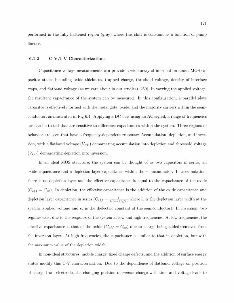
121
performed in the fully flattened region (gray) where this shift is constant as a function of pump
fluence.
6.1.2 C-V/I-V Characterizations
Capacitance-voltage measurements can provide a wide array of information about MOS ca-
pacitor stacks including oxide thickness, trapped charge, threshold voltage, density of interface
traps, and flatband voltage (as we care about in our studies) [259]. In varying the applied voltage,
the resultant capacitance of the system can be measured. In this configuration, a parallel plate
capacitor is effectively formed with the metal gate, oxide, and the majority carriers within the semi-
conductor, as illustrated in Fig 6.4. Applying a DC bias using an AC signal, a range of frequencies
are can be tested that are sensitive to difference capacitances within the system. Three regions of
behavior are seen that have a frequency-dependent response: Accumulation, depletion, and inver-
sion, with a flatband voltage (VFB) demarcating accumulation into depletion and threshold voltage
(VTH) demarcating depletion into inversion.
In an ideal MOS structure, the system can be thought of as two capacitors in series, an
oxide capacitance and a depletion layer capacitance within the semiconductor. In accumulation,
there is no depletion layer and the effective capacitance is equal to the capacitance of the oxide
(Ceff = Cox). In depletion, the effective capacitance is the addition of the oxide capacitance and
depletion layer capacitance in series (Ceff = 11/Cox+ld/εs
where ld is the depletion layer width at the
specific applied voltage and εs is the dielectric constant of the semiconductor). In inversion, two
regimes exist due to the response of the system at low and high frequencies. At low frequencies, the
effective capacitance is that of the oxide (Ceff = Cox) due to charge being added/removed from
the inversion layer. At high frequencies, the capacitance is similar to that in depletion, but with
the maximum value of the depletion width.
In non-ideal structures, mobile charge, fixed charge defects, and the addition of surface energy
states modify this C-V characterization. Due to the dependence of flatband voltage on position
of charge from electrode, the changing position of mobile charge with time and voltage leads to
122
Capacitance
Voltage Bias+Vg‐Vg
Depletion
Accumulation Inversion
0
Accumulation
Depletion Inversion
Vg < Vfb
Vfb< Vg < VT VT < Vg
Vg = Vfb
Flatband
EF
EF EF
EC
EV
Ei
EF
MetalInsulator
P‐typeSemiconductor
+ + + + +‐
+C‐Meter (AC Signal)
Low frequency
High frequency
Figure 6.4: C-V measurement technique (with measurement circuit shown top) and correspondingband diagrams (right) under accumulation, flatband, depletion, and inversion. White and blackpoints represent holes and electrons, respectively. Left panel adapted from [259].
capacitance shifts dependent on the sign of the charge and hysteresis changes. Fixed charge in the
oxide shifts the measured curve along the voltage axis. This shift reduces linearly as the position
of the charge relative to the gate is reduced (starting at metal-oxide interface). Fixed charge can
be due to incorporation during deposition or formation during processing. The response of these
charges and interface states is also frequency dependent. At high frequencies, the interface traps
are not able to respond fast enough to the AC signal to be filled, making their contribution to the
overall capacitance approach zero. The interface states only respond to the slowly changing DC
bias and act as a fixed charge within the stack, stretching out the C-V curve along the horizontal
axis [260]. At low frequencies, these charges are able to respond and give a “false inversion”-like
behavior. For a more in depth discussion of trapped charge within III-V gate stacks, the reader is
referred to Ref [261, 262, 263].
Common techniques to quantify the density of the interface states [249, 263] using values
obtained from C-Vs have been highly debated in III-V systems due to the common, usually dramatic
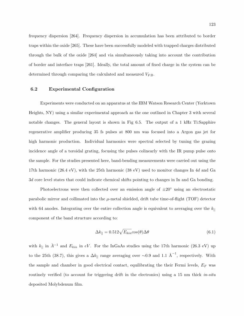
123
frequency dispersion [264]. Frequency dispersion in accumulation has been attributed to border
traps within the oxide [265]. These have been successfully modeled with trapped charges distributed
through the bulk of the oxide [264] and via simultaneously taking into account the contribution
of border and interface traps [261]. Ideally, the total amount of fixed charge in the system can be
determined through comparing the calculated and measured VFB.
6.2 Experimental Configuration
Experiments were conducted on an apparatus at the IBM Watson Research Center (Yorktown
Heights, NY) using a similar experimental approach as the one outlined in Chapter 3 with several
notable changes. The general layout is shown in Fig 6.5. The output of a 1 kHz Ti:Sapphire
regenerative amplifier producing 35 fs pulses at 800 nm was focused into a Argon gas jet for
high harmonic production. Individual harmonics were spectral selected by tuning the grazing
incidence angle of a toroidal grating, focusing the pulses colinearly with the IR pump pulse onto
the sample. For the studies presented here, band-bending measurements were carried out using the
17th harmonic (26.4 eV), with the 25th harmonic (38 eV) used to monitor changes In 4d and Ga
3d core level states that could indicate chemical shifts pointing to changes in In and Ga bonding.
Photoelectrons were then collected over an emission angle of ±20 using an electrostatic
parabolic mirror and collimated into the µ-metal shielded, drift tube time-of-flight (TOF) detector
with 64 anodes. Integrating over the entire collection angle is equivalent to averaging over the k||
component of the band structure according to:
∆k|| = 0.512√Ekincos(θ)∆θ (6.1)
with k|| in A−1 and Ekin in eV . For the InGaAs studies using the 17th harmonic (26.3 eV) up
to the 25th (38.7), this gives a ∆k|| range averaging over ∼0.9 and 1.1 A−1
, respectively. With
the sample and chamber in good electrical contact, equilibrating the their Fermi levels, EF was
routinely verified (to account for triggering drift in the electronics) using a 15 nm thick in-situ
deposited Molybdenum film.
124
TOF detector
sample
Electrostatic parabolic mirror
UHV Chamber
Ar jet
Pump pulse 1.55 eV (~35fs)
High Harmonic Generation
e-
High KE
Probe pulse25 - 40 eV
e-µ metal shielding
Figure 6.5: Experimental setup for band flattening studies. Notable differences from previousstudies include the use of a gas jet for HHG and an angle-integrated time-of-flight detector. Adaptedwith permission from [266]
In0.53Ga0.47As samples of 1µm thickness were prepared by MOCVD on InP(001) substrates
with a nominal doping of 6 ∗ 1016/cm2 for both n-type (Si doped) and p-type (Zn doped). For
the deposition-stage studies, new samples were simply removed after the high-κ growth process
and after the metal gate deposition. A (NH4)2S-last ex-situ treatment was used to remove native
oxides on the InGaAs surface and passivate the surface with sulfur. This was followed by air
transfer to an atomic layer deposition (ALD) tool within a few minutes, and ALD growth of
the high-k layer at 300 C. High-k thicknesses of 2 nm and 4 nm were grown of either Al2O3 or
HfO2 to have a direct comparison of thickness dependence and elemental oxide composition on
the charge defect behavior. Thicknesses were verified with Rutherford backscattering spectrometry
to be within 0.1 nm of the nominal value. With no additional surface preparation, 5 nm of TiN
was then grown via Physical Vapor Deposition (PVD) at room temperature on top of the high-
κ layer. All samples studied, including wafers undergoing patterning for MOScap samples, were
batch-processed at each step to minimize potential variations due to any potential process drift
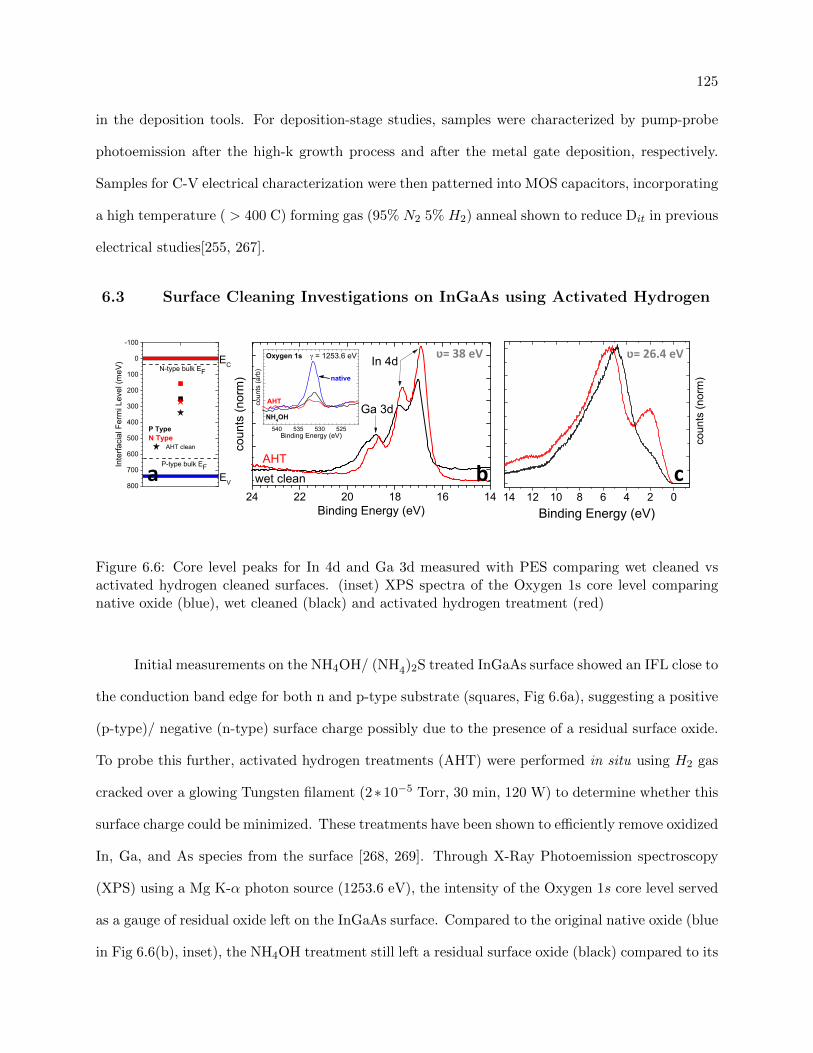
125
in the deposition tools. For deposition-stage studies, samples were characterized by pump-probe
photoemission after the high-k growth process and after the metal gate deposition, respectively.
Samples for C-V electrical characterization were then patterned into MOS capacitors, incorporating
a high temperature ( > 400 C) forming gas (95% N2 5% H2) anneal shown to reduce Dit in previous
electrical studies[255, 267].
6.3 Surface Cleaning Investigations on InGaAs using Activated Hydrogen
141618202224
coun
ts (n
orm
)
In 4d
Binding Energy (eV)
Ga 3d
wet cleanAHT
525530535540
coun
ts (a
rb)
native
Binding Energy (eV)
Oxygen 1s
NH4OH
AHT
= 1253.6 eV
02468101214
coun
ts (n
orm
)
Binding Energy (eV)
ʋ= 26.4 eVʋ= 38 eV-100
0
100
200
300
400
500
600
700
800
N-type bulk EF
EV
P-type bulk EFInte
rfaci
al F
erm
i Lev
el (m
eV) EC
P TypeN Type
AHT clean
a b c
Figure 6.6: Core level peaks for In 4d and Ga 3d measured with PES comparing wet cleaned vsactivated hydrogen cleaned surfaces. (inset) XPS spectra of the Oxygen 1s core level comparingnative oxide (blue), wet cleaned (black) and activated hydrogen treatment (red)
Initial measurements on the NH4OH/ (NH4)2S treated InGaAs surface showed an IFL close to
the conduction band edge for both n and p-type substrate (squares, Fig 6.6a), suggesting a positive
(p-type)/ negative (n-type) surface charge possibly due to the presence of a residual surface oxide.
To probe this further, activated hydrogen treatments (AHT) were performed in situ using H2 gas
cracked over a glowing Tungsten filament (2∗10−5 Torr, 30 min, 120 W) to determine whether this
surface charge could be minimized. These treatments have been shown to efficiently remove oxidized
In, Ga, and As species from the surface [268, 269]. Through X-Ray Photoemission spectroscopy
(XPS) using a Mg K-α photon source (1253.6 eV), the intensity of the Oxygen 1s core level served
as a gauge of residual oxide left on the InGaAs surface. Compared to the original native oxide (blue
in Fig 6.6(b), inset), the NH4OH treatment still left a residual surface oxide (black) compared to its
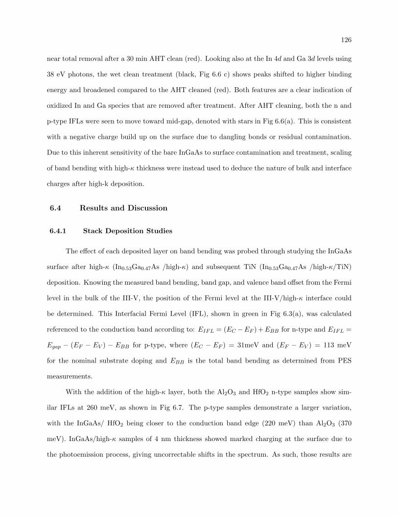
126
near total removal after a 30 min AHT clean (red). Looking also at the In 4d and Ga 3d levels using
38 eV photons, the wet clean treatment (black, Fig 6.6 c) shows peaks shifted to higher binding
energy and broadened compared to the AHT cleaned (red). Both features are a clear indication of
oxidized In and Ga species that are removed after treatment. After AHT cleaning, both the n and
p-type IFLs were seen to move toward mid-gap, denoted with stars in Fig 6.6(a). This is consistent
with a negative charge build up on the surface due to dangling bonds or residual contamination.
Due to this inherent sensitivity of the bare InGaAs to surface contamination and treatment, scaling
of band bending with high-κ thickness were instead used to deduce the nature of bulk and interface
charges after high-k deposition.
6.4 Results and Discussion
6.4.1 Stack Deposition Studies
The effect of each deposited layer on band bending was probed through studying the InGaAs
surface after high-κ (In0.53Ga0.47As /high-κ) and subsequent TiN (In0.53Ga0.47As /high-κ/TiN)
deposition. Knowing the measured band bending, band gap, and valence band offset from the Fermi
level in the bulk of the III-V, the position of the Fermi level at the III-V/high-κ interface could
be determined. This Interfacial Fermi Level (IFL), shown in green in Fig 6.3(a), was calculated
referenced to the conduction band according to: EIFL = (EC −EF ) +EBB for n-type and EIFL =
Egap − (EF − EV ) − EBB for p-type, where (EC − EF ) = 31meV and (EF − EV ) = 113 meV
for the nominal substrate doping and EBB is the total band bending as determined from PES
measurements.
With the addition of the high-κ layer, both the Al2O3 and HfO2 n-type samples show sim-
ilar IFLs at 260 meV, as shown in Fig 6.7. The p-type samples demonstrate a larger variation,
with the InGaAs/ HfO2 being closer to the conduction band edge (220 meV) than Al2O3 (370
meV). InGaAs/high-κ samples of 4 nm thickness showed marked charging at the surface due to
the photoemission process, giving uncorrectable shifts in the spectrum. As such, those results are
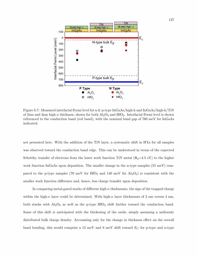
127
-100
0
100
200
300
400
500
600
700
800
N-type bulk EF
EV
P-type bulk EFInte
rfaci
al F
erm
i Lev
el (m
eV) EC
P Type Al2O3
HfO2
N TypeAl2O3
HfO2
(2 nm) High‐ κTiN
InGaAs InGaAs InGaAs(4 nm) High‐ κ
TiN(2 nm) High‐ κ
Figure 6.7: Measured interfacial Fermi level for n & p-type InGaAs/high-k and InGaAs/high-k/TiNof 2nm and 4nm high-κ thickness, shown for both Al2O3 and HfO2. Interfacial Fermi level is shownreferenced to the conduction band (red band), with the nominal band gap of 760 meV for InGaAsindicated.
not presented here. With the addition of the TiN layer, a systematic shift in IFLs for all samples
was observed toward the conduction band edge. This can be understood in terms of the expected
Schottky transfer of electrons from the lower work function TiN metal (Φp=4.5 eV) to the higher
work function InGaAs upon deposition. The smaller change in the n-type samples (55 meV) com-
pared to the p-type samples (70 meV for HfO2 and 140 meV for Al2O3) is consistent with the
smaller work function difference and, hence, less charge transfer upon deposition.
In comparing metal-gated stacks of different high-κ thicknesses, the sign of the trapped charge
within the high-κ layer could be determined. With high-κ layer thicknesses of 2 nm versus 4 nm,
both stacks with Al2O3 as well as the p-type HfO2 shift further toward the conduction band.
Some of this shift is anticipated with the thickening of the oxide, simply assuming a uniformly
distributed bulk charge density. Accounting only for the change in thickness effect on the overall
band bending, this would comprise a 12 meV and 8 meV shift toward EC for p-type and n-type
128
Al2O3 stacks, respectively. Instead, a shift of 140 meV (p-type) and 85 meV (n-type) is seen.
Similarly for HfO2 stacks, due to its high dielectric constant, a < 5 meV shift is expected for the
increased thickness. This is compared to the 60 meV shift measured for p-type, with a negligible
shift actually measured in the n-type stack. Since the samples were deposited with identical TiN,
the origin of this excess change to band bending must reside within the oxide. The increase in
band bending for the p-type and corresponding decrease in the n-type stacks indicate a positive
trapped charge. This is in agreement with electrical characterizations in previous work studying
III-V/high-κ/metal gate stacks that found positive trapped charge within HfO2 stacks [31] and
positive bulk/ negative interfacial charge in Al2O3 stacks [270, 260].
6.4.2 Thermal Treatment of stacks
Knowing the positive nature of the trapped charge within the oxide, its stability and evolution
could be probed as a function of thermal annealing to simulate processing conditions. Annealing
was done using direct current heating for 5 seconds at each subsequent temperature, with PES
measurements performed at room temperature. Several key aspects were seen in the behavior of
the IFL with annealing temperature, shown in Fig 6.8. First, the non metal-gated Al2O3 samples
(Fig 6.8a) demonstrated clear trends in both p and n-type stacks with the IFL showing a near
linear dependence with increasing temperature. 1
Two dominant regions of behavior are seen for the InGaAs/ high-κ/TiN stacks, denoted
in white and gray background, with a more dramatic trend seen in Al2O3 stacks. In the low
temperature region below 300-350C, IFLs for both 2 nm and 4 nm stacks move toward mid gap
with increasing temperature. Due to the initial presence of positive charge within the oxide, this
indicates a decrease in the magnitude of this charge. At higher temperatures above 350C, the IFL
moved back toward the conduction band, indicating an increase in the magnitude of the positive
charge within the oxide. The less dominant trend seen in HfO2 stacks (Fig 6.8d) supports previous
1 Due to the insulating nature of the high-κ layer, the as-received room temperature measurement (20 C) wassensitive to charges associated with adsorbed surface contamination like water and hydrocarbons. XPS verified a 200C anneal was sufficient in removing the majority of carbon contamination from the surface, yielding accurate bandbending measurements in the > 200C region.
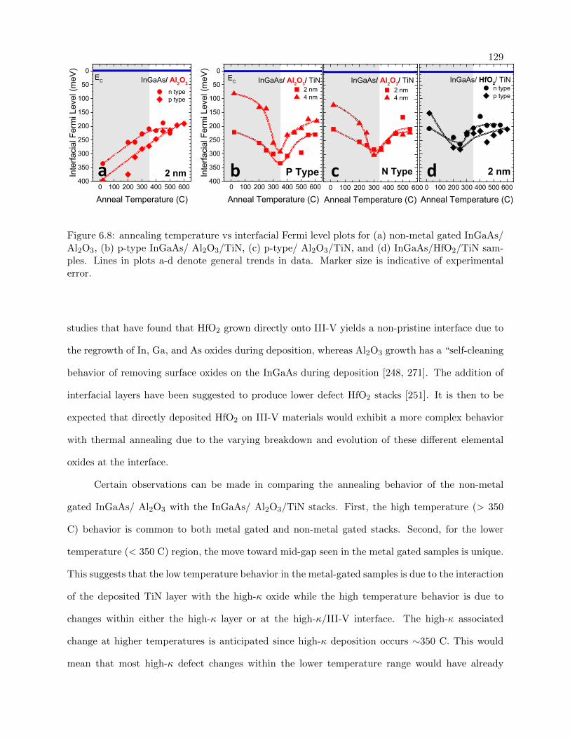
129
0 100 200 300 400 500 600
InGaAs/ Al2O3/ TiN
Anneal Temperature (C)
N Type
2 nm4 nm
0 100 200 300 400 500 600
0
50
100
150
200
250
300
350
400
EC
Anneal Temperature (C)
InGaAs/ Al2O3
Inte
rfaci
al F
erm
i Lev
el (m
eV)
n type p type
2 nm0 100 200 300 400 500 600
Anneal Temperature (C)
2 nm
InGaAs/ HfO2/ TiNn typep type
0 100 200 300 400 500 600
0
50
100
150
200
250
300
350
400
EC
Anneal Temperature (C)
InGaAs/ Al2O3/ TiN
Inte
rfaci
al F
erm
i Lev
el (m
eV)
2 nm4 nm
P Typea b c d
Figure 6.8: annealing temperature vs interfacial Fermi level plots for (a) non-metal gated InGaAs/Al2O3, (b) p-type InGaAs/ Al2O3/TiN, (c) p-type/ Al2O3/TiN, and (d) InGaAs/HfO2/TiN sam-ples. Lines in plots a-d denote general trends in data. Marker size is indicative of experimentalerror.
studies that have found that HfO2 grown directly onto III-V yields a non-pristine interface due to
the regrowth of In, Ga, and As oxides during deposition, whereas Al2O3 growth has a “self-cleaning
behavior of removing surface oxides on the InGaAs during deposition [248, 271]. The addition of
interfacial layers have been suggested to produce lower defect HfO2 stacks [251]. It is then to be
expected that directly deposited HfO2 on III-V materials would exhibit a more complex behavior
with thermal annealing due to the varying breakdown and evolution of these different elemental
oxides at the interface.
Certain observations can be made in comparing the annealing behavior of the non-metal
gated InGaAs/ Al2O3 with the InGaAs/ Al2O3/TiN stacks. First, the high temperature (> 350
C) behavior is common to both metal gated and non-metal gated stacks. Second, for the lower
temperature (< 350 C) region, the move toward mid-gap seen in the metal gated samples is unique.
This suggests that the low temperature behavior in the metal-gated samples is due to the interaction
of the deposited TiN layer with the high-κ oxide while the high temperature behavior is due to
changes within either the high-κ layer or at the high-κ/III-V interface. The high-κ associated
change at higher temperatures is anticipated since high-κ deposition occurs ∼350 C. This would
mean that most high-κ defect changes within the lower temperature range would have already
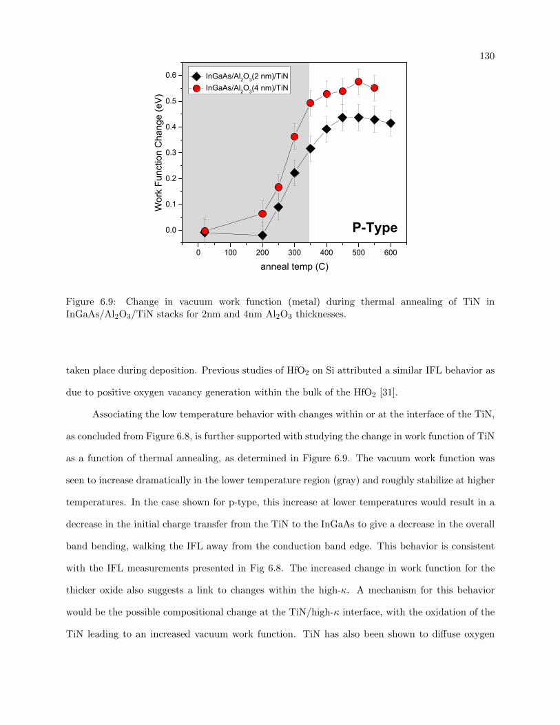
130
0 100 200 300 400 500 600
0.0
0.1
0.2
0.3
0.4
0.5
0.6
Wor
k Fu
nctio
n C
hang
e (e
V)
anneal temp (C)
InGaAs/Al2O3(2 nm)/TiN InGaAs/Al2O3(4 nm)/TiN
P-Type
Figure 6.9: Change in vacuum work function (metal) during thermal annealing of TiN inInGaAs/Al2O3/TiN stacks for 2nm and 4nm Al2O3 thicknesses.
taken place during deposition. Previous studies of HfO2 on Si attributed a similar IFL behavior as
due to positive oxygen vacancy generation within the bulk of the HfO2 [31].
Associating the low temperature behavior with changes within or at the interface of the TiN,
as concluded from Figure 6.8, is further supported with studying the change in work function of TiN
as a function of thermal annealing, as determined in Figure 6.9. The vacuum work function was
seen to increase dramatically in the lower temperature region (gray) and roughly stabilize at higher
temperatures. In the case shown for p-type, this increase at lower temperatures would result in a
decrease in the initial charge transfer from the TiN to the InGaAs to give a decrease in the overall
band bending, walking the IFL away from the conduction band edge. This behavior is consistent
with the IFL measurements presented in Fig 6.8. The increased change in work function for the
thicker oxide also suggests a link to changes within the high-κ. A mechanism for this behavior
would be the possible compositional change at the TiN/high-κ interface, with the oxidation of the
TiN leading to an increased vacuum work function. TiN has also been shown to diffuse oxygen
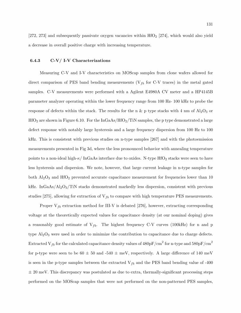
131
[272, 273] and subsequently passivate oxygen vacancies within HfO2 [274], which would also yield
a decrease in overall positive charge with increasing temperature.
6.4.3 C-V/ I-V Characterizations
Measuring C-V and I-V characteristics on MOScap samples from clone wafers allowed for
direct comparison of PES band bending measurements (Vfb for C-V traces) in the metal gated
samples. C-V measurements were performed with a Agilent E4980A CV meter and a HP4145B
parameter analyzer operating within the lower frequency range from 100 Hz- 100 kHz to probe the
response of defects within the stack. The results for the n & p type stacks with 4 nm of Al2O3 or
HfO2 are shown in Figure 6.10. For the InGaAs/HfO2/TiN samples, the p type demonstrated a large
defect response with notably large hysteresis and a large frequency dispersion from 100 Hz to 100
kHz. This is consistent with previous studies on n-type samples [267] and with the photoemission
measurements presented in Fig 3d, where the less pronounced behavior with annealing temperature
points to a non-ideal high-κ/ InGaAs interface due to oxides. N-type HfO2 stacks were seen to have
less hysteresis and dispersion. We note, however, that large current leakage in n-type samples for
both Al2O3 and HfO2 prevented accurate capacitance measurement for frequencies lower than 10
kHz. InGaAs/Al2O3/TiN stacks demonstrated markedly less dispersion, consistent with previous
studies [275], allowing for extraction of Vfb to compare with high temperature PES measurements.
Proper Vfb extraction method for III-V is debated [276], however, extracting corresponding
voltage at the theoretically expected values for capacitance density (at our nominal doping) gives
a reasonably good estimate of Vfb. The highest frequency C-V curves (100kHz) for n and p
type Al2O3 were used in order to minimize the contribution to capacitance due to charge defects.
Extracted Vfb for the calculated capacitance density values of 480pF/cm2 for n-type and 580pF/cm2
for p-type were seen to be 60 ± 50 and -540 ± meV, respectively. A large difference of 140 meV
is seen in the p-type samples between the extracted Vfb and the PES band bending value of -400
± 20 meV. This discrepancy was postulated as due to extra, thermally-significant processing steps
performed on the MOScap samples that were not performed on the non-patterned PES samples,
132
InGaA
s/Al
2O3/TiN
InGaA
s/HfO
2/TiN
-1.5 -1.0 -0.5 0.0 0.5 1.00.0
400.0n
800.0n
1.2µ
1.6µ
2.0µ
2.4µ Capacitance D
ensity (F/cm2)
Gate Bias (V)
0.0
400.0n
800.0n
1.2µ
1.6µ Capacitance D
ensity (F/cm2)
100 kHz10 kHz1 kHz100 Hz
P TypeN Type
-1.0 -0.5 0.0 0.5 1.0 1.5Gate Bias (V)
-1.5 -1.0 -0.5 0.0 0.5 1.0Gate bias (V)
10-7
10-6
10-5
10-4
10-3
10-2
10-1
100
101
Current D
ensity (A/cm2)
-1.5 -1.0 -0.5 0.0 0.5 1.010-8
10-7
10-6
10-5
10-4
10-3
10-2
Current D
ensity (A /cm2)
Gate bias (V)
InGaA
s/Al
2O3/TiN
InGaA
s/HfO
2/TiN
N Type P Type
Figure 6.10: (left) C-V characterization for p-type and n-type InGaAs/4 nm high-κ/5nm TiN stackswith Al2O3 and HfO2 measured at room temperature. Extracted Vfb values for Al2O3 samples aredenoted with dashed lines. (right) corresponding I-V characterizations.
namely a high temperature (> 400C) forming gas anneal. To test this, a forming gas anneal under
identical conditions was performed on the p-type sample and the band bending remeasured with
photoemission. With the p-type sample, the measured post-forming gas anneal value of 480 ± 20
meV was closer to the MOScap Vfb than pre-forming gas anneal, demonstrating agreement between
the extracted Vfb in electrical characterization and PES measurements as long as all processing
steps were replicated. The remaining discrepancy of 60 meV between PES and C-V measurements
accounts for a defect density of only 3 ∗ 1011/cm2. Due to this increase in Vfb and positive charge
known to be residing within the oxide, two possible scenarios can be occurring upon forming
gas annealing. First, there could be an addition of positive charge to the stack due to creation
of additional oxygen vacancies during the prolonged elevated temperature exposure of the oxide.
Otherwise, hydrogen would need to passivate a negative charge residing within the stack. Recent
theory [247] and electrical characterizations [270] of InGaAs/ Al2O3/TiN stacks have indicated a
133
possible positive charge within an Al-rich bulk portion of the oxide and a negative charge along an
O-rich interface. Upon forming gas anneal then, hydrogen passivates dangling bonds and decreases
negative charge along the interface. While either scenario is possible, additional studies on hydrogen
passivation of defects [255] point to the latter as the most probable mechanism.
6.5 Conclusions
Our studies have identified three unique stages effecting a net positive charge within InGaAs/high-
κ/TiN gate stacks, incorporating Al2O3 and HfO2, after deposition and thermal treatment:
(1) Charge transfer upon metal deposition between the TiN and InGaAs due to dissimilar work
functions.
(2) A low temperature region (< 350 C) decreasing net positive charge associated with changes
at the TiN/high-κ interface.
(3) A high temperature region (> 350 C) increasing net positive charge associated with changes
within the high-κ itself.
Furthermore, photoemission band bending measurements used to discern these behaviors
show good agreement with conventional C-V measurements on identical wafers after similar pro-
cessing.
Chapter 7
Future Outlook and Conclusions
Several of the experiments in this presented work can benefit from two milestones that have
recently (within < 2 years) been realized in high harmonic generation: (1) high energy-resolution
harmonics driven with 2ω light [14] and (2) the successful demonstration of circular harmonics
[277]. The following sections outline the extension of presented experiments possible utilizing these
techniques, followed by general conclusions of the work presented in this thesis.
7.1 Circular harmonic Generation
In the traditional description of laser–driven high harmonic generation, a circularly polarized
driving field fails to produce harmonics due to the initially ionized electron never being able to trace
a path to recollide with its parent ion. However, as theoretical descriptions [278, 50] and a recent
experimental implementation [277] have shown, this restriction can be overcome by wave-mixing of
two disparate driving frequencies. Driven with copropogating 400 nm and 800 nm light of opposite
helicity, the resultant electric field component traces out a Lissajous curve, or trefoil shape, that
produces three linear bursts of harmonics that rotate over one optical cycle (shown in Fig 7.1, left).
Yielding a pulse train that contains alternating left circular polarization (LCP) and right-circular
polarization (RCP) (shown in Fig 7.1 right), these effectively circular harmonics have been used in
magnetic circular dichroism (MCD) measurements on Co [277] to demonstrate their potential for
future material applications.
With the benefit of generating circularly polarized harmonics comes tremendous potential
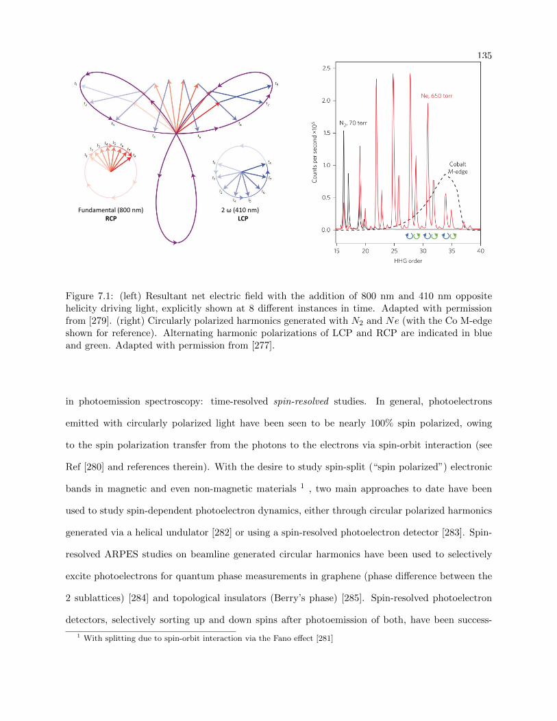
135
Fundamental (800 nm)RCP
2 ω (410 nm)LCP
Figure 7.1: (left) Resultant net electric field with the addition of 800 nm and 410 nm oppositehelicity driving light, explicitly shown at 8 different instances in time. Adapted with permissionfrom [279]. (right) Circularly polarized harmonics generated with N2 and Ne (with the Co M-edgeshown for reference). Alternating harmonic polarizations of LCP and RCP are indicated in blueand green. Adapted with permission from [277].
in photoemission spectroscopy: time-resolved spin-resolved studies. In general, photoelectrons
emitted with circularly polarized light have been seen to be nearly 100% spin polarized, owing
to the spin polarization transfer from the photons to the electrons via spin-orbit interaction (see
Ref [280] and references therein). With the desire to study spin-split (“spin polarized”) electronic
bands in magnetic and even non-magnetic materials 1 , two main approaches to date have been
used to study spin-dependent photoelectron dynamics, either through circular polarized harmonics
generated via a helical undulator [282] or using a spin-resolved photoelectron detector [283]. Spin-
resolved ARPES studies on beamline generated circular harmonics have been used to selectively
excite photoelectrons for quantum phase measurements in graphene (phase difference between the
2 sublattices) [284] and topological insulators (Berry’s phase) [285]. Spin-resolved photoelectron
detectors, selectively sorting up and down spins after photoemission of both, have been success-
1 With splitting due to spin-orbit interaction via the Fano effect [281]
136
fully used to map spin-polarized band structures in materials [286, 287]. However, these systems
are usually characterized by a lower throughput efficiency (and hence lower number of collected
photoelectron events), making time-resolved material studies difficult. Spin-resolved studies have
also mapped the transient valence band structure of Gd(0001) during a ultrafast demagnetization
process [288], but the large exchange splitting of the bands made explicit spin-resolved detection
not necessary.
7.1.1 RABITT studies on Cu(111)
In the RABITT measurements presented in Chapter 4, the interfering sidebands of the comb
of generated harmonics allowed both the intrinsic chirp of the harmonics and quantum phase of
the valence Cu(111) states to be measured. Following its original prescription to be used in char-
acterizing the harmonic comb, a similar experiment can be conducted on Cu(111) to characterize
the chirp and generation of the comb of circular harmonics. Investigations are already underway
and have revealed relative phase delays between harmonics of opposite helicity.
In addition to characterization of the harmonics themselves, the presented studies revealing
information on the electronic states of Cu(111) can be extended to other material systems. Of
particular interest is the extension of the metallic valence band studies in Chapter 4 to include
dielectric systems. With, for example, Xe adsorbed onto Cu(111), any screening effects contribut-
ing to the metallic Cu(111) dynamics can be minimized due to the near-unity dielectric constant.
Preliminary work done on Xe overlayers on Mg(111) in the context of free-electron classical trans-
port through the overlayer using attosecond streaking [100]. The electron interferometry technique
employed here would allow for a more detailed study comparing the conduction band dynamics of
the underlying Cu(111) surface with the Xe bands, provided the Xe adlayer was sufficiently thin to
be able to simultaneously resolve bands from both materials.
137
7.1.2 Graphene
In the measurements presented on Graphene in Chapter 5, photoemission with linear polar-
ized harmonics only allowed for the study of electron dynamics in Graphene/SiC(0001) and studies
on the modification of graphene’s electronic structure with the addition of alkali adsorbates. In
using our linearly polarized harmonics, modeling the specific form of the transition matrix elements
that would otherwise allow us to directly extract the phase, is made difficult by experimental inten-
sity fluctuations and accounting for all final state effects [289]. By spin-selectively photoemitting
electrons via circular harmonics, these issues can be minimized. Static spin-resolved ARPES mea-
surements on Graphene using circularly polarized harmonics have been used to directly extract
the Berry’s phase of both mono and bilayer Graphene [284, 290], with good agreement to the-
ory. Electron dynamics using linear harmonics have also been mapped in Graphene/SiC(0001) and
Graphene/Ni(111), showing little deviation from similar measurements on graphitic systems.
To date however, these two studies have not been combined, where the tracking the spin-
resolved electron dynamics of graphene have not been directly probed with ARPES. These types of
studies would be able to inform on spin-dependent scattering processing such as Elliott-Yafet and
Dyakonov-Perel mechanisms. Elliot-Yafet scattering refers to a “spin flip” mechanism mediated
by scattering with impurities, defects, or phonons while Dyakonov-Perel scattering results in elec-
trons feeling an effective magnetic field, that changes in direction upon each momentum-changing
scattering event, resulting in random spin precession [291, 292]. These mechanisms act on different
momentum scattering times [293], allowing one to determine the relative contributions to graphene’s
overall electron dynamics if probed on a sufficiently fast timescale. Indirect measurements [291, 294]
have attempted to determine which spin scattering mechanism is dominant, with results suggesting
a prominent Elliott-Yafet contribution. These dynamics would be directly accessible using circu-
larly polarized harmonics in graphene photoemission studies. Furthermore, these studies could be
extended to adsorbate modified graphene systems, like H-terminated “graphane”, where the con-
trolled addition of impurities and modification of graphene’s electronic structure would influence
138
the dominant spin-scattering timescales [295].
7.1.3 Topological Insulators
In the same vein as the graphene system, topological insulators, whose band structures exhibit
a similar Dirac cone feature to that of graphene, have attracted considerable interest for ARPES
studies recently [296, 297, 298]. Previous time-resolved studies of have used circular polarized
pump excitations to study exotic phenomena such as driven spin-polarized photocurrents [299],
induced band gap opening [296], and temporally mapping the spin “texture” of the dirac cone
[297]. Unlike graphene, the surface helical Dirac fermions (as measured over the Fermi surface) in
topological insulators interact with phonons as well as electrons from the bulk reservoir [300, 298].
Attempts at disentangling these interactions by resolving these electron dynamics has been done
via spin resolved reflectivity measurements [301] or a circularly polarized excitation [298]. With
the addition of a circularly polarized probe, the spin topography of this band structure could be
mapped more precisely over time.
7.1.4 Surface-Adsorbate Systems
Additionally, studies have even seen spin-dependent charge transport for surface-adsorbate
systems like Ar adsorbed onto Fe(110), Co(0001), and Ni(111) [302]. These studies found a faster
charge transfer for minority electrons in the Fe and Co systems, with little difference in the Ni
system. With the transfer time difference attributed to the relative abundance of empty electronic
states in the material, similar studies can be performed to directly probe the spin state of the
system over the course of the ultrafast (2-3 fs) charge transfer. Similar dynamical studies on spin-
resolved relaxation can be used to study the substrate-induced polarization of adatoms [303] and
spin-polarized auger electron processes [282]
139
7.2 Time-resolved High energy-resolution Studies
With the implementation of narrow energy-bandwidth (< 150 meV), high photon energy (21
[14] - 60 eV [73]) harmonics, previous limitations for choosing experimental systems with widely-
separated band structure features are greatly lifted. With these narrow harmonics measured to
have a pulse length of 20 fs, this also gives enough temporal resolution to capture all but the
fastest of electron dynamics.
7.2.1 Directly resolving interface states in InGaAs
Of particular interest, is directly resolving the dynamics of defect interface states in InGaAs.
In the studies presented in Chapter 6, the number of charged defects in a MOS stack are quantified
as they evolve with addition of deposited layers and annealing temperature. One remaining piece
of this puzzle is the nature of the electronic interface states themselves: What is the density of
trap states in the InGaAs band gap? It there a dominant interface state? What is the timescale in
which these defect states fill and empty with carriers? A dominant interface state could contribute
to “pinning” the Fermi level in InGaAs [304, 305], a concern in being able to tune the electronic
bands with an applied bias and calling into question its viability for use in MOSFET devices.
Direct evidence for these interface states have been seen in Inverse photoemission studies on GaAs
[306] and electron microscopy [307], but the exact occupation and density of states is seen to
vary greatly with surface preparation and interface quality [308]. Probing the distribution and
dynamics of these narrow bandwidth states upon carrier relaxation can therefore help in mapping
the dominant scattering mechanisms and timescales that are important for understanding electronic
device performance.
Similar to the studies proposed in Section 7.1.2, GaAs has also been seen to exhibit a photo-
induced spin Hall effect, where spin-oriented optically excited surface electrons diffuse into the
bulk via spin-dependent scattering [309, 299]. The relaxation dynamics of these electrons has been
measured through time-resolved Faraday rotation [310] to be exceptionally long (10-100 ns) due to
140
lack of spin-orbit coupling in its conduction band. The dominant mechanism in this spin scattering
band has been suggested to be temperature dependent as well, with Dyakonov-Perel transitioning
to Elliott-Yafet at low temperatures [311]. As such, a temperature dependent, spin-resolved study
of carrier dynamics in GaAs and III-V family materials will be useful in determining the relative
contributions of these processes to carrier relaxation.
7.3 Conclusion
This thesis employed high-harmonic driven ARPES to measure electronic properties of ma-
terials from metallic surfaces to post-silicon technologies like Graphene and III-V structures. The
experimental implementations utilized range from the conventional pump-probe scheme for time-
resolved carrier dynamics studies, to attosecond spectroscopy and photovoltage band flattening
techniques to measure fundamental electronic state phases and device-inhibiting charge defects.
These results serve as a springboard for further study utilizing the recently developed techniques
of narrow energy-bandwidth and circularly polarized high harmonics.
Bibliography
[1] H. Petek and S. Ogawa, “FEMTOSECOND TIME-RESOLVED PHOTOEMISSION STUD-IES OF ELECTRON DYNAMICS IN METALS,” Progress in Surface Science, vol. 56, no. 4,pp. 239–310, 1997.
[2] J. C. Miller and R. F. Haglund Laser Ablation and Desorption, no. Academic Press, Boston,1997.
[3] E. Beaurepaire, J.-C. Merle, a. Daunois, and J.-Y. Bigot, “Ultrafast Spin Dynamics in Fer-romagnetic Nickel,” Physical Review Letters, vol. 76, pp. 4250–4253, May 1996.
[4] R. Cavanagh, D. King, J. Stephenson, and T. Heinz, “Dynamics of Nonthermal Reactions :Femtosecond Surface Chemistry,” J. Phys. Chem, vol. 97, pp. 786–798, 1993.
[5] N. Aschroft and N. Mermin Solid State Physics, no. Holt, Rinehart, Winston, Hong Kong,1987.
[6] T. Haarlammert and H. Zacharias, “Application of high harmonic radiation in surface sci-ence,” Current Opinion in Solid State and Materials Science, vol. 13, pp. 13–27, Feb. 2009.
[7] R. Tobin, “VIBRATIONAL LINEWIDTHS OF ADSORBED MOLECULES: EXPERIMEN-TAL CONSIDERATIONS AND RESULTS,” Surface Science, vol. 183, pp. 226–250, 1987.
[8] M. Bonn, S. Funk, C. Hess, D. Denzler, C. Stampfl, M. Scheffler, M. Wolf, and G. Ertl,“Phonon- Versus Electron-Mediated Desorption and Oxidation of CO on,” Science, vol. 285,no. August, pp. 1042–1045, 1999.
[9] K. Zhao, Q. Zhang, M. Chini, Y. Wu, X. Wang, and Z. Chang, “Tailoring a 67 attosecondpulse through advantageous phase-mismatch,” Optics L, vol. 37, no. 18, pp. 3891–3893, 2012.
[10] M. Chini, B. Zhao, H. Wang, Y. Cheng, S. X. Hu, and Z. Chang, “Subcycle ac Stark Shiftof Helium Excited States Probed with Isolated Attosecond Pulses,” Physical Review Letters,vol. 109, p. 073601, Aug. 2012.
[11] C. Spielmann, N. H. Burnett, S. Sartania, R. Koppitsch, C. Kan, M. Lenzner, P. Wobrauschek,and F. Krausz, “Generation of Coherent X-rays in the Water Window Using 5-FemtosecondLaser Pulses,” Science, vol. 278, no. October, 1997.
142
[12] T. Popmintchev, M.-c. Chen, D. Popmintchev, P. Arpin, S. Brown, S. Ali, G. Andriukaitis,T. Bal, O. D. Mucke, A. Pugzlys, A. Baltu, B. Shim, S. E. Schrauth, A. Gaeta, C. Hernandez-garcıa, L. Plaja, A. Becker, A. Jaron-becker, M. M. Murnane, and H. C. Kapteyn, “BrightCoherent Ultrahigh Harmonics in the keV X-ray Regime from Mid-Infrared FemtosecondLasers,” Science, vol. 336, pp. 1287–1291, 2012.
[13] S. Mathias, L. Miaja-Avila, M. M. Murnane, H. Kapteyn, M. Aeschlimann, and M. Bauer,“Angle-resolved photoemission spectroscopy with a femtosecond high harmonic light sourceusing a two-dimensional imaging electron analyzer.,” The Review of scientific instruments,vol. 78, p. 083105, Aug. 2007.
[14] S. Eich, a. Stange, a.V. Carr, J. Urbancic, T. Popmintchev, M. Wiesenmayer, K. Jansen,a. Ruffing, S. Jakobs, T. Rohwer, S. Hellmann, C. Chen, P. Matyba, L. Kipp, K. Rossnagel,M. Bauer, M. Murnane, H. Kapteyn, S. Mathias, and M. Aeschlimann, “Time- and angle-resolved photoemission spectroscopy with optimized high-harmonic pulses using frequency-doubled Ti:Sapphire lasers,” Journal of Electron Spectroscopy and Related Phenomena,vol. 195, pp. 231–236, Aug. 2014.
[15] R. Haight, J. a. Silberman, and M. I. Lilie, “Novel system for picosecond photoemissionspectroscopy,” Review of Scientific Instruments, vol. 59, no. 9, p. 1941, 1988.
[16] M. Bauer, C. Lei, K. Read, R. Tobey, J. Gland, M. Murnane, and H. Kapteyn, “Direct Ob-servation of Surface Chemistry Using Ultrafast Soft-X-Ray Pulses,” Physical Review Letters,vol. 87, p. 025501, June 2001.
[17] T. Rohwer, S. Hellmann, M. Wiesenmayer, C. Sohrt, A. Stange, B. Slomski, A. Carr, Y. Liu,L. M. Avila, M. Kallane, S. Mathias, L. Kipp, K. Rossnagel, and M. Bauer, “Collapse oflong-range charge order tracked by time-resolved photoemission at high momenta,” Nature,vol. 471, pp. 490–493, Mar. 2011.
[18] A. Melzer, D. Kampa, J. Wang, and T. Fauster, “Time-resolved photoemission at the Si(100)-Ga surface using a femtosecond higher-harmonic laser source,” Physical Review B, vol. 80,p. 205424, Nov. 2009.
[19] R. Jiang, D. Mou, Y. Wu, L. Huang, C. D. McMillen, J. Kolis, H. G. Giesber, J. J. Egan,and A. Kaminski, “Tunable vacuum ultraviolet laser based spectrometer for angle resolvedphotoemission spectroscopy.,” The Review of scientific instruments, vol. 85, p. 033902, Mar.2014.
[20] L. Perfetti, P. a. Loukakos, M. Lisowski, U. Bovensiepen, H. Eisaki, and M. Wolf, “UltrafastElectron Relaxation in Superconducting Bi 2Sr 2CaCu 2O 8+δ by Time-ResolvedPhotoelectron Spectroscopy,” Physical Review Letters, vol. 99, p. 197001, Nov. 2007.
[21] W. Ackermann, G. Asova, V. Ayvazyan, a. Azima, N. Baboi, J. Bahr, V. Balandin, B. Beut-ner, a. Brandt, a. Bolzmann, R. Brinkmann, O. I. Brovko, M. Castellano, P. Castro, L. Catani,E. Chiadroni, S. Choroba, a. Cianchi, J. T. Costello, D. Cubaynes, J. Dardis, W. Decking,H. Delsim-Hashemi, a. Delserieys, G. Di Pirro, M. Dohlus, S. Dusterer, a. Eckhardt, H. T.Edwards, B. Faatz, J. Feldhaus, K. Flottmann, J. Frisch, L. Frohlich, T. Garvey, U. Gen-sch, C. Gerth, M. Gorler, N. Golubeva, H.-J. Grabosch, M. Grecki, O. Grimm, K. Hacker,U. Hahn, J. H. Han, K. Honkavaara, T. Hott, M. Huning, Y. Ivanisenko, E. Jaeschke,
143
W. Jalmuzna, T. Jezynski, R. Kammering, V. Katalev, K. Kavanagh, E. T. Kennedy,S. Khodyachykh, K. Klose, V. Kocharyan, M. Korfer, M. Kollewe, W. Koprek, S. Korepanov,D. Kostin, M. Krassilnikov, G. Kube, M. Kuhlmann, C. L. S. Lewis, L. Lilje, T. Limberg,D. Lipka, F. Lohl, H. Luna, M. Luong, M. Martins, M. Meyer, P. Michelato, V. Miltchev,W. D. Moller, L. Monaco, W. F. O. Muller, O. Napieralski, O. Napoly, P. Nicolosi, D. Nolle,T. Nunez, a. Oppelt, C. Pagani, R. Paparella, N. Pchalek, J. Pedregosa-Gutierrez, B. Pe-tersen, B. Petrosyan, G. Petrosyan, L. Petrosyan, J. Pfluger, E. Plonjes, L. Poletto, K. Poz-niak, E. Prat, D. Proch, P. Pucyk, P. Radcliffe, H. Redlin, K. Rehlich, M. Richter, M. Roehrs,J. Roensch, R. Romaniuk, M. Ross, J. Rossbach, V. Rybnikov, M. Sachwitz, E. L. Saldin,W. Sandner, H. Schlarb, B. Schmidt, M. Schmitz, P. Schmuser, J. R. Schneider, E. a. Schnei-dmiller, S. Schnepp, S. Schreiber, M. Seidel, D. Sertore, a. V. Shabunov, C. Simon, S. Sim-rock, E. Sombrowski, a. a. Sorokin, P. Spanknebel, R. Spesyvtsev, L. Staykov, B. Steffen,F. Stephan, F. Stulle, H. Thom, K. Tiedtke, M. Tischer, S. Toleikis, R. Treusch, D. Trines,I. Tsakov, E. Vogel, T. Weiland, H. Weise, M. Wellhofer, M. Wendt, I. Will, a. Winter,K. Wittenburg, W. Wurth, P. Yeates, M. V. Yurkov, I. Zagorodnov, and K. Zapfe, “Op-eration of a free-electron laser from the extreme ultraviolet to the water window,” NaturePhotonics, vol. 1, pp. 336–342, June 2007.
[22] S. Hellmann, M. Beye, C. Sohrt, T. Rohwer, F. Sorgenfrei, H. Redlin, M. Kallane,M. Marczynski-Buhlow, F. Hennies, M. Bauer, a. Fohlisch, L. Kipp, W. Wurth, and K. Ross-nagel, “Ultrafast Melting of a Charge-Density Wave in the Mott Insulator 1T-TaS 2,”Physical Review Letters, vol. 105, p. 187401, Oct. 2010.
[23] M. Dell’Angela, T. Anniyev, M. Beye, R. Coffee, J. Gladh, T. Katayama, S. Kaya, O. Krupin,J. Larue, D. Nordlund, H. Ogasawara, L. G. M. Pettersson, W. F. Schlotter, J. A. Sellberg,F. Sorgenfrei, J. J. Turner, M. Wolf, W. Wurth, and A. Nilsson, “Real-Time Observation ofSurface Bond Breaking with an X-ray Laser,” Science, vol. 959, no. March, pp. 1302–1306,2013.
[24] M. Drescher, M. Hentschel, R. Kienberger, M. Uiberacker, V. Yakovlev, a. Scrinzi, T. West-erwalbesloh, U. Kleineberg, U. Heinzmann, and F. Krausz, “Time-resolved atomic inner-shellspectroscopy.,” Nature, vol. 419, pp. 803–7, Oct. 2002.
[25] B. Goldstein and D. Szostak, “SURFACE PHOTOVOLTAGE, BAND-BENDING AND SUR-FACE STATES ON aSi:H*,” Surface Science, vol. 99, pp. 235–258, 1980.
[26] L. Kronik and Y. Shapira, “Surface photovoltage phenomena : theory , experiment , andapplications,” Surface Science Reports, vol. 37, pp. 1–206, 1999.
[27] C. Marchiori, M. El Kazzi, L. Czornomaz, D. Pierucci, M. Silly, F. Sirotti, S. Abel, E. Uccelli,M. Sousa, and J. Fompeyrine, “Nanoscale physics and defect state chemistry at amorphous-Si/In 0.53 Ga 0.47 As interfaces,” Journal of Physics D: Applied Physics, vol. 47, p. 055101,Feb. 2014.
[28] J. Demuth, W. Thompson, N. DiBardo, and R. Imbihl, “Photoemission-Based PhotovoltageProbe of Semiconductor Surface and Interface Electronic Structure,” Physical Review Letters,vol. 56, no. 13, pp. 1408–1411, 1986.
[29] W. Widdra, D. Brocker, T. Gieß el, I. Hertel, W. Kruger, a. Liero, F. Noack, V. Petrov,D. Pop, P. Schmidt, R. Weber, I. Will, and B. Winter, “Time-resolved core level photoemis-
144
sion: surface photovoltage dynamics of the SiO2/Si(100) interface,” Surface Science, vol. 543,pp. 87–94, Oct. 2003.
[30] H. Arimura, R. Haight, S. L. Brown, A. Kellock, A. Callegari, M. Copel, H. Watanabe,V. Narayanan, and T. Ando, “Temperature-dependent La- and Al-induced dipole behav-ior monitored by femtosecond pump/probe photoelectron spectroscopy,” Applied PhysicsLetters, vol. 96, no. 13, p. 132902, 2010.
[31] D. Lim, R. Haight, M. Copel, and E. Cartier, “Oxygen defects and Fermi level location inmetal-hafnium oxide-silicon structures,” Applied Physics Letters, vol. 87, no. 7, p. 072902,2005.
[32] H. P. Bonzel and C. H. Kleint, “On the history of photoemission,” Progress in Surface Science,vol. 49, no. 2, pp. 107–153, 1995.
[33] M. Helander, M. Greiner, Z. Wang, and Z. Lu, “Pitfalls in measuring work function usingphotoelectron spectroscopy,” Applied Surface Science, vol. 256, pp. 2602–2605, Feb. 2010.
[34] J. Sitte, “Relation between reference levels, work functions, and contact potential differencein photoelectron spectroscopy,” Chemical Physics Letters, vol. 42, no. 1, pp. 131–132, 1976.
[35] A. Damascelli, Z. Hussain, and Z.-X. Shen, “Angle-resolved photoemission studies of thecuprate superconductors,” Reviews of Modern Physics, vol. 75, no. April, 2003.
[36] S. Hufner Photoemission Spectroscopy: Principles and Applications, no. 3rd Ed, Springer,2010.
[37] P. Feibelman and D. Eastman, “Photoemission spectroscopy Correspondence between quan-tum theory and experimental phenomenology,” Physical Review B, vol. 10, no. 12, 1974.
[38] A. Mcpherson, G. Gibson, H. Jara, U. Johann, T. S. Luk, I. A. Mcintyre, K. Boyer, andC. K. Rhodes, “Studies of multiphoton production of vacuum-ultraviolet radiation in therare gases,” Journal of Optical Society of America B, vol. 4, no. 4, pp. 595–601, 1987.
[39] Durfee, A. Rundquist, S. Backus, Z. Chang, C. Herne, H. Kapteyn, and M. Murnane, “Guidedwave phase matching of ultrashort pulse light,” Journal of Nonlinear Optical Physics andMaterials, vol. 8, no. 2, pp. 211–234, 1999.
[40] T. Pfeifer, C. Spielmann, and G. Gerber, “Femtosecond x-ray science,” Reports on Progressin Physics, vol. 69, pp. 443–505, Feb. 2006.
[41] J. J. Rocca, “Table-top soft x-ray lasers,” Review of Scientific Instruments, vol. 70, no. 10,p. 3799, 1999.
[42] M. Lewenstein, P. Balcou, M. Y. Ivanov, A. L. Huillier, and P. Corkum, “Theory of high-harmonic generation by low-frequency laser fields,” Physical Review A, vol. 49, no. 3, 1994.
[43] P. Corkum, “Plasma Perspective on Strong-Field Multiphoton Ionization,” Physical reviewletters, vol. 71, no. 13, pp. 1994–1997, 1993.
[44] S. K. J. Kulander K C and K. J. L, “Dynamics of short-pulse excitation, ionization andharmonic conversion,” Proc. Work-shop on Super-Intense Laser Atom Physics (SILAP) III,1993.
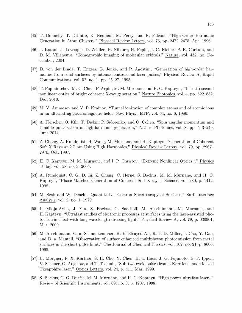
145
[45] T. Donnelly, T. Ditmire, K. Neuman, M. Perry, and R. Falcone, “High-Order HarmonicGeneration in Atom Clusters,” Physical Review Letters, vol. 76, pp. 2472–2475, Apr. 1996.
[46] J. Itatani, J. Levesque, D. Zeidler, H. Niikura, H. Pepin, J. C. Kieffer, P. B. Corkum, andD. M. Villeneuve, “Tomographic imaging of molecular orbitals,” Nature, vol. 432, no. De-cember, 2004.
[47] D. von der Linde, T. Engers, G. Jenke, and P. Agostini, “Generation of high-order har-monics from solid surfaces by intense femtosecond laser pulses,” Physical Review A, RapidCommunications, vol. 52, no. 1, pp. 25–27, 1995.
[48] T. Popmintchev, M.-C. Chen, P. Arpin, M. M. Murnane, and H. C. Kapteyn, “The attosecondnonlinear optics of bright coherent X-ray generation,” Nature Photonics, vol. 4, pp. 822–832,Dec. 2010.
[49] M. V. Ammosov and V. P. Krainov, “Tunnel ionization of complex atoms and of atomic ionsin an alternating electromagnetic field,” Sov. Phys. JETP, vol. 64, no. 6, 1986.
[50] A. Fleischer, O. Kfir, T. Diskin, P. Sidorenko, and O. Cohen, “Spin angular momentum andtunable polarization in high-harmonic generation,” Nature Photonics, vol. 8, pp. 543–549,June 2014.
[51] Z. Chang, A. Rundquist, H. Wang, M. Murnane, and H. Kapteyn, “Generation of CoherentSoft X Rays at 2.7 nm Using High Harmonics,” Physical Review Letters, vol. 79, pp. 2967–2970, Oct. 1997.
[52] H. C. Kapteyn, M. M. Murnane, and I. P. Christov, “Extreme Nonlinear Optics :,” PhysicsToday, vol. 58, no. 3, 2005.
[53] A. Rundquist, C. G. D. Iii, Z. Chang, C. Herne, S. Backus, M. M. Murnane, and H. C.Kapteyn, “Phase-Matched Generation of Coherent Soft X-rays,” Science, vol. 280, p. 1412,1998.
[54] M. Seah and W. Dench, “Quantitative Electron Spectroscopy of Surfaces,” Surf. InterfaceAnalysis, vol. 2, no. 1, 1979.
[55] L. Miaja-Avila, J. Yin, S. Backus, G. Saathoff, M. Aeschlimann, M. Murnane, andH. Kapteyn, “Ultrafast studies of electronic processes at surfaces using the laser-assisted pho-toelectric effect with long-wavelength dressing light,” Physical Review A, vol. 79, p. 030901,Mar. 2009.
[56] M. Aeschlimann, C. a. Schmuttenmaer, H. E. Elsayed-Ali, R. J. D. Miller, J. Cao, Y. Gao,and D. a. Mantell, “Observation of surface enhanced multiphoton photoemission from metalsurfaces in the short pulse limit,” The Journal of Chemical Physics, vol. 102, no. 21, p. 8606,1995.
[57] U. Morgner, F. X. Kartner, S. H. Cho, Y. Chen, H. a. Haus, J. G. Fujimoto, E. P. Ippen,V. Scheuer, G. Angelow, and T. Tschudi, “Sub-two-cycle pulses from a Kerr-lens mode-lockedTi:sapphire laser,” Optics Letters, vol. 24, p. 411, Mar. 1999.
[58] S. Backus, C. G. Durfee, M. M. Murnane, and H. C. Kapteyn, “High power ultrafast lasers,”Review of Scientific Instruments, vol. 69, no. 3, p. 1207, 1998.
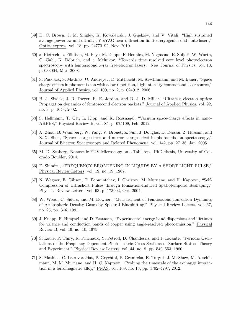
146
[59] D. C. Brown, J. M. Singley, K. Kowalewski, J. Guelzow, and V. Vitali, “High sustainedaverage power cw and ultrafast Yb:YAG near-diffraction-limited cryogenic solid-state laser.,”Optics express, vol. 18, pp. 24770–92, Nov. 2010.
[60] a. Pietzsch, a. Fohlisch, M. Beye, M. Deppe, F. Hennies, M. Nagasono, E. Suljoti, W. Wurth,C. Gahl, K. Dobrich, and a. Melnikov, “Towards time resolved core level photoelectronspectroscopy with femtosecond x-ray free-electron lasers,” New Journal of Physics, vol. 10,p. 033004, Mar. 2008.
[61] S. Passlack, S. Mathias, O. Andreyev, D. Mittnacht, M. Aeschlimann, and M. Bauer, “Spacecharge effects in photoemission with a low repetition, high intensity femtosecond laser source,”Journal of Applied Physics, vol. 100, no. 2, p. 024912, 2006.
[62] B. J. Siwick, J. R. Dwyer, R. E. Jordan, and R. J. D. Miller, “Ultrafast electron optics:Propagation dynamics of femtosecond electron packets,” Journal of Applied Physics, vol. 92,no. 3, p. 1643, 2002.
[63] S. Hellmann, T. Ott, L. Kipp, and K. Rossnagel, “Vacuum space-charge effects in nano-ARPES,” Physical Review B, vol. 85, p. 075109, Feb. 2012.
[64] X. Zhou, B. Wannberg, W. Yang, V. Brouet, Z. Sun, J. Douglas, D. Dessau, Z. Hussain, andZ.-X. Shen, “Space charge effect and mirror charge effect in photoemission spectroscopy,”Journal of Electron Spectroscopy and Related Phenomena, vol. 142, pp. 27–38, Jan. 2005.
[65] M. D. Seaberg, Nanoscale EUV Microscopy on a Tabletop. PhD thesis, University of Col-orado Boulder, 2014.
[66] F. Shimizu, “FREQUENCY BROADENING IN LIQUIDS BY A SHORT LIGHT PULSE,”Physical Review Letters, vol. 19, no. 19, 1967.
[67] N. Wagner, E. Gibson, T. Popmintchev, I. Christov, M. Murnane, and H. Kapteyn, “Self-Compression of Ultrashort Pulses through Ionization-Induced Spatiotemporal Reshaping,”Physical Review Letters, vol. 93, p. 173902, Oct. 2004.
[68] W. Wood, C. Siders, and M. Downer, “Measurement of Femtosecond Ionization Dynamicsof Atmospheric Density Gases by Spectral Blueshifting,” Physical Review Letters, vol. 67,no. 25, pp. 3–6, 1991.
[69] J. Knapp, F. Himpsel, and D. Eastman, “Experimental energy band dispersions and lifetimesfor valence and conduction bands of copper using angle-resolved photoemission,” PhysicalReview B, vol. 19, no. 10, 1979.
[70] S. Louie, P. Thiry, R. Pinchaux, Y. Petroff, D. Chandesris, and J. Lecante, “Periodic Oscil-lations of the Frequency-Dependent Photoelectric Cross Sections of Surface States: Theoryand Experiment,” Physical Review Letters, vol. 44, no. 8, pp. 549–553, 1980.
[71] S. Mathias, C. La-o vorakiat, P. Grychtol, P. Granitzka, E. Turgut, J. M. Shaw, M. Aeschli-mann, M. M. Murnane, and H. C. Kapteyn, “Probing the timescale of the exchange interac-tion in a ferromagnetic alloy,” PNAS, vol. 109, no. 13, pp. 4792–4797, 2012.
147
[72] L. X. Yang, G. Rohde, T. Rohwer, A. Stange, K. Hanff, C. Sohrt, L. Rettig, R. Cortes,F. Chen, D. L. Feng, T. Wolf, B. Kamble, I. Eremin, T. Popmintchev, M. M. Murnane, H. C.Kapteyn, L. Kipp, J. Fink, M. Bauer, U. Bovensiepen, and K. Rossnagel, “Ultrafast Modu-lation of the Chemical Potential in BaFe2As,” Physical Review Letters, vol. 112, p. 207001,May 2014.
[73] K. Ishizaka, T. Kiss, T. Yamamoto, Y. Ishida, T. Saitoh, M. Matsunami, R. Eguchi, T. Oht-suki, a. Kosuge, T. Kanai, M. Nohara, H. Takagi, S. Watanabe, and S. Shin, “Femtosecondcore-level photoemision spectroscopy on 1T-TaS 2 using a 60-eV laser source,” PhysicalReview B, vol. 83, p. 081104, Feb. 2011.
[74] G. M. Blumenstock, M. L. Gintert, and R. Meski-Kuha, “Extreme ultraviolet optical proper-ties of ion-beam-deposited boron carbide thin films,” Proc. SPIE 2515, X-Ray and ExtremeUltraviolet Optics, no. 558, pp. 558–564, 1995.
[75] E. M. G. B. L. Henke and J. C. Davis, “X-Ray Interactions: Photoabsorption, Scattering,Transmission, and Reflection at E = 5030,000 eV, Z = 192,” At. Data Nucl. Data Tables,vol. 54, no. 181, 1993.
[76] M. Nisoli, S. D. Silvestri, O. Svelto, and R. Szip, “Compression of high-energy laser pulsesbelow 5 fs,” Optics Letters, vol. 22, no. 8, pp. 522–524, 1997.
[77] A. Borzsonyi, Z. Heiner, a. P. Kovacs, M. P. Kalashnikov, and K. Osvay, “Measurementof pressure dependent nonlinear refractive index of inert gases.,” Optics express, vol. 18,pp. 25847–54, Dec. 2010.
[78] L.-l. Gottingen, “Hollow-fiber pulse compressor for KrF lasers,” Applied Physics B, vol. 82,pp. 567–570, 2006.
[79] P. Bejot, J. Kasparian, S. Henin, V. Loriot, T. Vieillard, E. Hertz, O. Faucher, B. Lavorel,and J.-P. Wolf, “Higher-Order Kerr Terms Allow Ionization-Free Filamentation in Gases,”Physical Review Letters, vol. 104, p. 103903, Mar. 2010.
[80] A. Suda, M. Hatayama, K. Nagasaka, and K. Midorikawa, “Generation of sub-10-fs, 5-mJ-optical pulses using a hollow fiber with a pressure gradient,” Applied Physics Letters, vol. 86,no. 11, p. 111116, 2005.
[81] J. a. R. Samson and H. Liebl, “Duoplasmatron as a Vacuum Ultraviolet Light Source,” Reviewof Scientific Instruments, vol. 33, no. 12, p. 1340, 1962.
[82] C.-f. Lei, “Using ultrafast extreme-ultraviolet pulses for time-resolved dynamics of moleculeschemisorbed on metal surfaces,” PhD Thesis, 2003.
[83] S. Mahl, “Phoibos Hemispherical Analyzer Series: Phoibos 100 documentation,” Specs Gmbh,2013.
[84] C.-M. Cheng, “Angle–resolved photoemission spectroscopy resolved photoemission spec-troscopy (ARPES) for 2D layered structure : graphene and topological insulators,” NTHUSemianr, 2013.
148
[85] P. D. C. King, R. C. Hatch, M. Bianchi, R. Ovsyannikov, C. Lupulescu, G. Landolt, B. Slom-ski, J. H. Dil, D. Guan, J. L. Mi, E. D. L. Rienks, J. Fink, a. Lindblad, S. Svensson,S. Bao, G. Balakrishnan, B. B. Iversen, J. Osterwalder, W. Eberhardt, F. Baumberger, andP. Hofmann, “Large Tunable Rashba Spin Splitting of a Two-Dimensional Electron Gas inBi 2Se 3,” Physical Review Letters, vol. 107, p. 096802, Aug. 2011.
[86] a. Fohlisch, P. Feulner, F. Hennies, a. Fink, D. Menzel, D. Sanchez-Portal, P. M. Echenique,and W. Wurth, “Direct observation of electron dynamics in the attosecond domain.,” Nature,vol. 436, pp. 373–6, July 2005.
[87] F. Calegari, D. Ayuso, a. Trabattoni, L. Belshaw, S. De Camillis, S. Anumula, F. Frassetto,L. Poletto, a. Palacios, P. Decleva, J. B. Greenwood, F. Martın, and M. Nisoli, “Ultrafast elec-tron dynamics in phenylalanine initiated by attosecond pulses.,” Science (New York, N.Y.),vol. 346, pp. 336–9, Oct. 2014.
[88] H. Wang, M. Chini, S. Chen, C.-H. Zhang, F. He, Y. Cheng, Y. Wu, U. Thumm, andZ. Chang, “Attosecond Time-Resolved Autoionization of Argon,” Physical Review Letters,vol. 105, p. 143002, Oct. 2010.
[89] a. L. Cavalieri, N. Muller, T. Uphues, V. S. Yakovlev, a. Baltuska, B. Horvath, B. Schmidt,L. Blumel, R. Holzwarth, S. Hendel, M. Drescher, U. Kleineberg, P. M. Echenique, R. Kien-berger, F. Krausz, and U. Heinzmann, “Attosecond spectroscopy in condensed matter.,”Nature, vol. 449, pp. 1029–32, Oct. 2007.
[90] S. Neppl, R. Ernstorfer, E. M. Bothschafter, a. L. Cavalieri, D. Menzel, J. V. Barth, F. Krausz,R. Kienberger, and P. Feulner, “Attosecond Time-Resolved Photoemission from Core andValence States of Magnesium,” Physical Review Letters, vol. 109, p. 087401, Aug. 2012.
[91] S. Neppl, R. Ernstorfer, a. L. Cavalieri, C. Lemell, G. Wachter, E. Magerl, E. M. Bothschafter,M. Jobst, M. Hofstetter, U. Kleineberg, J. V. Barth, D. Menzel, J. Burgdorfer, P. Feulner,F. Krausz, and R. Kienberger, “Direct observation of electron propagation and dielectricscreening on the atomic length scale,” Nature, vol. 517, pp. 342–346, Jan. 2015.
[92] M. Schultze, M. Fiess, N. Karpowicz, J. Gagnon, M. Korbman, M. Hofstetter, S. Neppl, a. L.Cavalieri, Y. Komninos, T. Mercouris, C. a. Nicolaides, R. Pazourek, S. Nagele, J. Feist,J. Burgdorfer, a. M. Azzeer, R. Ernstorfer, R. Kienberger, U. Kleineberg, E. Goulielmakis,F. Krausz, and V. S. Yakovlev, “Delay in photoemission.,” Science (New York, N.Y.), vol. 328,pp. 1658–62, June 2010.
[93] M. Swoboda, T. Fordell, K. Klunder, J. M. Dahlstrom, M. Miranda, C. Buth, K. J. Schafer,J. Mauritsson, a. LHuillier, and M. Gisselbrecht, “Phase Measurement of Resonant Two-Photon Ionization in Helium,” Physical Review Letters, vol. 104, p. 103003, Mar. 2010.
[94] C. Palatchi, J. M. Dahlstrom, a. S. Kheifets, I. a. Ivanov, D. M. Canaday, P. Agostini, andL. F. DiMauro, “Atomic delay in helium, neon, argon and krypton,” Journal of Physics B:Atomic, Molecular and Optical Physics, vol. 47, p. 245003, Dec. 2014.
[95] K. Klunder, J. M. Dahlstrom, M. Gisselbrecht, T. Fordell, M. Swoboda, D. Guenot, P. Johns-son, J. Caillat, J. Mauritsson, a. Maquet, R. Taıeb, and a. LHuillier, “Probing Single-PhotonIonization on the Attosecond Time Scale,” Physical Review Letters, vol. 106, p. 143002, Apr.2011.
149
[96] S. Haessler, B. Fabre, J. Higuet, J. Caillat, T. Ruchon, P. Breger, B. Carre, E. Constant,a. Maquet, E. Mevel, P. Salieres, R. Taıeb, and Y. Mairesse, “Phase-resolved attosecondnear-threshold photoionization of molecular nitrogen,” Physical Review A, vol. 80, p. 011404,July 2009.
[97] U. Heinzmann, “Attosecond Physics,” vol. 177, pp. 231–253, 2013.
[98] P. M. Paul, E. S. Toma, P. Breger, G. Mullot, F. Auge, P. Balcou, H. G. Muller, andP. Agostini, “Observation of a train of attosecond pulses from high harmonic generation.,”Science (New York, N.Y.), vol. 292, pp. 1689–92, June 2001.
[99] R. Lopez-Martens, K. Varju, P. Johnsson, J. Mauritsson, Y. Mairesse, P. Salieres, M. Gaarde,K. Schafer, A. Persson, S. Svanberg, C.-G. Wahlstrom, and A. LHuillier, “Amplitude andPhase Control of Attosecond Light Pulses,” Physical Review Letters, vol. 94, p. 033001, Jan.2005.
[100] S. Neppl, Attosecond Tme-Resolved Photoemission from Surfaces and Interfaces. PhD the-sis, Technische Universitat Munchen, 2012.
[101] A. Baltuska, T. Udem, M. Uiberacker, M. Hentschel, E. Goulielmakis, C. Gohle,R. Holzwarth, V. Yakovlev, A. Scrinzi, T. Hansch, and F. Krausz, “Attosecond control ofelectronic processes by intense light fields,” Nature, vol. 421, no. February, 2003.
[102] M. J. Abel, T. Pfeifer, P. M. Nagel, W. Boutu, M. J. Bell, C. P. Steiner, D. M. Neumark, andS. R. Leone, “Isolated attosecond pulses from ionization gating of high-harmonic emission,”Chemical Physics, vol. 366, no. 1-3, pp. 9–14, 2009.
[103] P. B. Corkum, N. H. Burnett, and M. Y. Ivanov, “Subfemtosecond pulses.,” Optics letters,vol. 19, no. 22, p. 1870, 1994.
[104] V. S. Yakovlev, J. Gagnon, N. Karpowicz, and F. Krausz, “Attosecond streaking enables themeasurement of quantum phase,” Physical Review Letters, vol. 105, no. August, pp. 3–6,2010.
[105] G. Saathoff, L. Miaja-Avila, M. Aeschlimann, M. Murnane, and H. Kapteyn, “Laser-assistedphotoemission from surfaces,” Physical Review A, vol. 77, p. 022903, Feb. 2008.
[106] L. Miaja-Avila, G. Saathoff, S. Mathias, J. Yin, C. La-o vorakiat, M. Bauer, M. Aeschlimann,M. Murnane, and H. Kapteyn, “Direct Measurement of Core-Level Relaxation Dynamics ona Surface-Adsorbate System,” Physical Review Letters, vol. 101, p. 046101, July 2008.
[107] C.-H. Zhang and U. Thumm, “Laser-assisted photoemission from adsorbate-covered metalsurfaces: Time-resolved core-hole relaxation dynamics from sideband profiles,” PhysicalReview A, vol. 80, p. 032902, Sept. 2009.
[108] H. Muller, “Reconstruction of attosecond harmonic beating by interference of two-photontransitions,” Applied Physics B, vol. 74, pp. s17–s21, Apr. 2002.
[109] K. Varju, P. Johnsson, T. Remetter, E. Gustafsson, E. Constant, E. Cormier, E. Mevel, andA. L. Huillier, “Experimental Studies of Attosecond Pulse Trains,” Laser Physics, vol. 15,no. 6, pp. 888–898, 2005.
150
[110] D. Guenot, K. Klunder, C. L. Arnold, D. Kroon, J. M. Dahlstrom, M. Miranda, T. Fordell,M. Gisselbrecht, P. Johnsson, J. Mauritsson, E. Lindroth, a. Maquet, R. Taıeb, a. LHuillier,and a. S. Kheifets, “Photoemission-time-delay measurements and calculations close to the 3s-ionization-cross-section minimum in Ar,” Physical Review A, vol. 85, p. 053424, May 2012.
[111] J. M. Dahlstrom, a. LHuillier, a. Maquet, H. Search, C. Journals, A. Contact, M. Iopscience,and I. P. Address, “Introduction to attosecond delays in photoionization,” Journal of PhysicsB: Atomic, Molecular and Optical Physics, vol. 45, p. 183001, 2012.
[112] J. Dahlstrom, T. Fordell, E. Mansten, T. Ruchon, M. Swoboda, K. Klunder, M. Gisselbrecht,a. LHuillier, and J. Mauritsson, “Atomic and macroscopic measurements of attosecond pulsetrains,” Physical Review A, vol. 80, p. 033836, Sept. 2009.
[113] D. Jones, S. Diddams, J. Ranka, a. Stentz, R. Windeler, J. Hall, and S. Cundiff, “Carrier-envelope phase control of femtosecond mode-locked lasers and direct optical frequency syn-thesis,” Science (New York, N.Y.), vol. 288, no. April, pp. 635–40, 2000.
[114] E. S. Toma and H. Muller, “Calculation of matrix elements for mixed extreme-ultravioletinfrared two-photon above-threshold ionization of argon,” Journal of Physics B:Atomic, Molecular and Optical Physics, vol. 35, pp. 3435–3442, 2002.
[115] V. Veniard, R. Taieb, and A. Maquet, “Phase dependence of (N+1) color (N¿1) ir-uv pho-toionization of atoms with higher harmonics,” Physical Review A, vol. 54, no. 1, pp. 721–728,1996.
[116] a. S. Kheifets and I. a. Ivanov, “Delay in atomic photoionization,” Physical Review Letters,vol. 105, no. December, pp. 1–4, 2010.
[117] a. S. Kheifets, “Time delay in valence-shell photoionization of noble-gas atoms,” PhysicalReview A - Atomic, Molecular, and Optical Physics, vol. 87, no. April, pp. 1–9, 2013.
[118] a. K. Kazansky and N. M. Kabachnik, “Sideband structure in angle-resolved electron spec-tra from laser-assisted Auger decay generated by ultra-short pulses,” Journal of Physics B:Atomic, Molecular and Optical Physics, vol. 42, p. 121002, June 2009.
[119] J. Baggesen and L. Madsen, “Theory for time-resolved measurements of laser-induced electronemission from metal surfaces,” Physical Review A, vol. 78, p. 032903, Sept. 2008.
[120] C.-H. Zhang and U. Thumm, “Attosecond Photoelectron Spectroscopy of Metal Surfaces,”Physical Review Letters, vol. 102, p. 123601, Mar. 2009.
[121] C.-H. Zhang and U. Thumm, “Effect of wave-function localization on the time delay inphotoemission from surfaces,” Physical Review A, vol. 84, p. 065403, Dec. 2011.
[122] C. Lemell, B. Solleder, K. Tkesi, and J. Burgdorfer, “Simulation of attosecond streaking ofelectrons emitted from a tungsten surface,” Physical Review A, vol. 79, p. 062901, June 2009.
[123] C.-H. Zhang and U. Thumm, “Probing dielectric-response effects with attosecond time-resolved streaked photoelectron spectroscopy of metal surfaces,” Physical Review A, vol. 84,p. 063403, Dec. 2011.
151
[124] L. Miaja-Avila, C. Lei, M. Aeschlimann, J. Gland, M. Murnane, H. Kapteyn, and G. Saathoff,“Laser-Assisted Photoelectric Effect from Surfaces,” Physical Review Letters, vol. 97,p. 113604, Sept. 2006.
[125] R. Courths, H. Wern, and S. Hufner, “THE TAMM SURFACE STATE ON Cu( 111) ANDAg( 111),” Solid State Communications, vol. 61, no. 4, pp. 257–260, 1987.
[126] A. Winkelmann, C. Tusche, a. Akin Unal, M. Ellguth, J. Henk, and J. Kirschner, “Analysis ofthe electronic structure of copper via two-dimensional photoelectron momentum distributionpatterns,” New Journal of Physics, vol. 14, p. 043009, Apr. 2012.
[127] N. Smith, R. Benbow, and Z. Hurych, “Photoemission spectra and band structures of d-bandmetals. VIII. Normal emission from Cu(111),” Physical Review B, vol. 21, no. 10, 1980.
[128] X. Li, Z. Zhang, and V. Henrich, “Inelastic Electron Background Function for UltravioletPhotoelectron-Spectra,” Journal of Electron Spectroscopy and Related Phenomena, vol. 63,pp. 253–265, 1993.
[129] J. Dahlstrom, D. Guenot, K. Klunder, M. Gisselbrecht, J. Mauritsson, a. LHuillier, a. Ma-quet, and R. Taıeb, “Theory of attosecond delays in laser-assisted photoionization,” ChemicalPhysics, vol. 414, pp. 53–64, Mar. 2013.
[130] E. P. Ma nsson, D. Guenot, C. L. Arnold, D. Kroon, S. Kasper, J. M. Dahlstrom, E. Lindroth,A. S. Kheifets, A. LHuillier, S. L. Sorensen, and M. Gisselbrecht, “Double ionization probedon the attosecond timescale,” Nature Physics, vol. 10, pp. 207–211, Jan. 2014.
[131] L. Schulz, “The Optical Constants of Silver, Gold, Copper, and Aluminum. I. The AbsorptionCoefficient k,” Journal of Optical Society of America, vol. 44, no. 5, 1954.
[132] A. Zangwill Physics at Surfaces, no. New York:Cambridge: University Press, p454, 1988.
[133] K. S. Novoselov, a. K. Geim, S. V. Morozov, D. Jiang, Y. Zhang, S. V. Dubonos, I. V.Grigorieva, and a. a. Firsov, “Electric field effect in atomically thin carbon films.,” Science(New York, N.Y.), vol. 306, pp. 666–9, Oct. 2004.
[134] K. S. Novoselov, a. K. Geim, S. V. Morozov, D. Jiang, M. I. Katsnelson, I. V. Grigorieva, S. V.Dubonos, and a. a. Firsov, “Two-dimensional gas of massless Dirac fermions in graphene.,”Nature, vol. 438, pp. 197–200, Nov. 2005.
[135] C. Berger, Z. Song, T. Li, X. Li, A. Y. Ogbazghi, R. Feng, Z. Dai, A. N. Marchenkov, E. H.Conrad, P. N. First, and W. A. D. Heer, “Ultrathin Epitaxial Graphite : 2D Electron GasProperties and a Route toward,” J. Phys. Chem. B, vol. 108, pp. 19912–19916, 2004.
[136] M. Batzill, “The surface science of graphene: Metal interfaces, CVD synthesis, nanoribbons,chemical modifications, and defects,” Surface Science Reports, vol. 67, pp. 83–115, Mar. 2012.
[137] Y. S. Dedkov, M. Fonin, and C. Laubschat, “A possible source of spin-polarized electrons:The inert graphene/Ni(111) system,” Applied Physics Letters, vol. 92, no. 5, p. 052506, 2008.
[138] K. Bolotin, K. Sikes, Z. Jiang, M. Klima, G. Fudenberg, J. Hone, P. Kim, and H. Stormer,“Ultrahigh electron mobility in suspended graphene,” Solid State Communications, vol. 146,pp. 351–355, June 2008.
152
[139] P. W. Sutter, J.-I. Flege, and E. a. Sutter, “Epitaxial graphene on ruthenium.,” Naturematerials, vol. 7, pp. 406–11, May 2008.
[140] C. Enderlein, Y. S. Kim, a. Bostwick, E. Rotenberg, and K. Horn, “The formation of anenergy gap in graphene on ruthenium by controlling the interface,” New Journal of Physics,vol. 12, p. 033014, Mar. 2010.
[141] M. Papagno, S. Rusponi, P. M. Sheverdyaeva, S. Vlaic, M. Etzkorn, D. Pacile, P. Moras,C. Carbone, and H. Brune, “Large band gap opening between graphene Dirac cones inducedby Na adsorption onto an Ir superlattice.,” ACS nano, vol. 6, pp. 199–204, Jan. 2012.
[142] T. Jayasekera, B. D. Kong, K. W. Kim, and M. Buongiorno Nardelli, “Band Engineering andMagnetic Doping of Epitaxial Graphene on SiC (0001),” Physical Review Letters, vol. 104,p. 146801, Apr. 2010.
[143] N. D. Mermin, “Crystalline Order in Two Dimensions,” Physical Review, vol. 176, no. 1,1968.
[144] K. S. Kim, Y. Zhao, H. Jang, S. Y. Lee, J. M. Kim, K. S. Kim, J.-H. Ahn, P. Kim, J.-Y. Choi,and B. H. Hong, “Large-scale pattern growth of graphene films for stretchable transparentelectrodes.,” Nature, vol. 457, pp. 706–10, Feb. 2009.
[145] Y. Lee, S. Bae, H. Jang, S. Jang, S.-E. Zhu, S. H. Sim, Y. I. Song, B. H. Hong, and J.-H.Ahn, “Wafer-scale synthesis and transfer of graphene films.,” Nano letters, vol. 10, pp. 490–3,Feb. 2010.
[146] T. J. Booth, P. Blake, R. R. Nair, D. Jiang, E. W. Hill, U. Bangert, A. Bleloch, M. Gass,K. S. Novoselov, M. I. Katsnelson, and a. K. Geim, “Macroscopic graphene membranes andtheir extraordinary stiffness.,” Nano letters, vol. 8, pp. 2442–6, Aug. 2008.
[147] http://www.elume.com/projects/organic semiconductors 2013.
[148] M. Mucha-Kruczyski, O. Tsyplyatyev, A. Grishin, E. McCann, V. Falko, A. Bostwick, andE. Rotenberg, “Characterization of graphene through anisotropy of constant-energy maps inangle-resolved photoemission,” Physical Review B, vol. 77, p. 195403, May 2008.
[149] A. Gruneis and D. Vyalikh, “Tunable hybridization between electronic states of graphene anda metal surface,” Physical Review B, vol. 77, p. 193401, May 2008.
[150] P. Avouris, “Graphene: Electronic and Photonic Properties and Devices.,” Nano letters,pp. 4285–4294, Sept. 2010.
[151] D. Boukhvalov, M. Katsnelson, and a. Lichtenstein, “Hydrogen on graphene: Electronic struc-ture, total energy, structural distortions and magnetism from first-principles calculations,”Physical Review B, vol. 77, p. 035427, Jan. 2008.
[152] T. Ohta, A. Bostwick, T. Seyller, K. Horn, and E. Rotenberg, “Controlling the electronicstructure of bilayer graphene.,” Science (New York, N.Y.), vol. 313, pp. 951–4, Aug. 2006.
[153] K. Nakada, M. Fujita, G. Dresselhaus, and M. Dresselhaus, “Edge state in graphene ribbons:Nanometer size effect and edge shape dependence,” Physical Review B, vol. 54, pp. 17954–17961, Dec. 1996.
153
[154] G. Giovannetti, P. Khomyakov, G. Brocks, V. Karpan, J. van den Brink, and P. Kelly,“Doping Graphene with Metal Contacts,” Physical Review Letters, vol. 101, p. 026803, July2008.
[155] a. K. Geim, “Graphene: status and prospects.,” Science (New York, N.Y.), vol. 324, pp. 1530–4, June 2009.
[156] S. Gilje, S. Han, M. Wang, K. L. Wang, and R. B. Kaner, “A chemical route to graphene fordevice applications.,” Nano letters, vol. 7, pp. 3394–8, Nov. 2007.
[157] K. R. Paton, E. Varrla, C. Backes, R. J. Smith, U. Khan, A. O’Neill, C. Boland, M. Lotya,O. M. Istrate, P. King, T. Higgins, S. Barwich, P. May, P. Puczkarski, I. Ahmed, M. Moebius,H. Pettersson, E. Long, J. a. Coelho, S. E. O’Brien, E. K. McGuire, B. M. Sanchez, G. S.Duesberg, N. McEvoy, T. J. Pennycook, C. Downing, A. Crossley, V. Nicolosi, and J. N.Coleman, “Scalable production of large quantities of defect-free few-layer graphene by shearexfoliation in liquids.,” Nature materials, vol. 13, pp. 624–30, June 2014.
[158] W. a. de Heer, C. Berger, X. Wu, P. N. First, E. H. Conrad, X. Li, T. Li, M. Sprinkle,J. Hass, M. L. Sadowski, M. Potemski, and G. Martinez, “Epitaxial graphene,” Solid StateCommunications, vol. 143, pp. 92–100, July 2007.
[159] K. V. Emtsev, A. Bostwick, K. Horn, J. Jobst, G. L. Kellogg, L. Ley, J. L. McChesney,T. Ohta, S. a. Reshanov, J. Rohrl, E. Rotenberg, A. K. Schmid, D. Waldmann, H. B. Weber,and T. Seyller, “Towards wafer-size graphene layers by atmospheric pressure graphitizationof silicon carbide.,” Nature materials, vol. 8, pp. 203–7, Mar. 2009.
[160] C. Berger, Z. Song, X. Li, X. Wu, N. Brown, C. Naud, D. Mayou, T. Li, J. Hass, A. N.Marchenkov, E. H. Conrad, P. N. First, and W. a. de Heer, “Electronic confinement andcoherence in patterned epitaxial graphene.,” Science (New York, N.Y.), vol. 312, pp. 1191–6,May 2006.
[161] Y.-W. Son, M. L. Cohen, and S. G. Louie, “Energy Gaps in Graphene Nanoribbons,” PhysicalReview Letters, vol. 97, p. 216803, Nov. 2006.
[162] M. Eizenberg and J. Blakely, “CARBON MONOLAYER PHASE CONDENSATION ON Ni(111),” Surface Science, vol. 82, pp. 228–236, 1979.
[163] A. NDiaye, S. Bleikamp, P. Feibelman, and T. Michely, “Two-Dimensional Ir Cluster Latticeon a Graphene Moire on Ir(111),” Physical Review Letters, vol. 97, p. 215501, Nov. 2006.
[164] T. A. Land, T. Michely, R. J. Behm, and J. C. Hemminger, “STM investigation of singlelayer graphite structures produced on Pt ( 111 ) by hydrocarbon decomposition,” SurfaceScience, vol. 264, pp. 261–270, 1992.
[165] L. Gao, J. R. Guest, and N. P. Guisinger, “Epitaxial graphene on Cu(111).,” Nano letters,vol. 10, pp. 3512–6, Sept. 2010.
[166] Q. Yu, J. Lian, S. Siriponglert, H. Li, Y. P. Chen, and S.-S. Pei, “Graphene segregated on Nisurfaces and transferred to insulators,” Applied Physics Letters, vol. 93, no. 11, p. 113103,2008.
154
[167] W. Regan, N. Alem, B. Aleman, B. Geng, C. Girit, L. Maserati, F. Wang, M. Crommie, anda. Zettl, “A direct transfer of layer-area graphene,” Applied Physics Letters, vol. 96, no. 11,p. 113102, 2010.
[168] M. Breusing, S. Kuehn, T. Winzer, E. Malic, F. Milde, N. Severin, J. P. Rabe, C. Ropers,a. Knorr, and T. Elsaesser, “Ultrafast nonequilibrium carrier dynamics in a single graphenelayer,” Physical Review B, vol. 83, p. 153410, Apr. 2011.
[169] D. Brida, a. Tomadin, C. Manzoni, Y. J. Kim, a. Lombardo, S. Milana, R. R. Nair, K. S.Novoselov, a. C. Ferrari, G. Cerullo, and M. Polini, “Ultrafast collinear scattering and carriermultiplication in graphene.,” Nature communications, vol. 4, p. 1987, Jan. 2013.
[170] J. M. Dawlaty, S. Shivaraman, M. Chandrashekhar, F. Rana, and M. G. Spencer, “Measure-ment of ultrafast carrier dynamics in epitaxial graphene,” Applied Physics Letters, vol. 92,no. 4, p. 042116, 2008.
[171] P. a. George, J. Strait, J. Dawlaty, S. Shivaraman, M. Chandrashekhar, F. Rana, and M. G.Spencer, “Ultrafast optical-pump terahertz-probe spectroscopy of the carrier relaxation andrecombination dynamics in epitaxial graphene.,” Nano letters, vol. 8, pp. 4248–51, Dec. 2008.
[172] T. Li, L. Luo, M. Hupalo, J. Zhang, M. C. Tringides, J. Schmalian, and J. Wang, “Femtosec-ond Population Inversion and Stimulated Emission of Dense Dirac Fermions in Graphene,”Physical Review Letters, vol. 108, p. 167401, Apr. 2012.
[173] S.-F. Shi, T.-T. Tang, B. Zeng, L. Ju, Q. Zhou, a. Zettl, and F. Wang, “Controlling grapheneultrafast hot carrier response from metal-like to semiconductor-like by electrostatic gating.,”Nano letters, vol. 14, pp. 1578–82, Mar. 2014.
[174] I. Gierz, J. C. Petersen, M. Mitrano, C. Cacho, I. C. E. Turcu, E. Springate, A. Stohr,A. Kohler, U. Starke, and A. Cavalleri, “Snapshots of non-equilibrium Dirac carrier distribu-tions in graphene.,” Nature materials, vol. 12, pp. 1119–24, Dec. 2013.
[175] J. C. Johannsen, S. r. Ulstrup, F. Cilento, A. Crepaldi, M. Zacchigna, C. Cacho, I. C. E. Turcu,E. Springate, F. Fromm, C. Raidel, T. Seyller, F. Parmigiani, M. Grioni, and P. Hofmann,“Direct View of Hot Carrier Dynamics in Graphene,” Physical Review Letters, vol. 111,p. 027403, July 2013.
[176] T. Someya, H. Fukidome, Y. Ishida, R. Yoshida, T. Iimori, R. Yukawa, K. Akikubo, S. Ya-mamoto, S. Yamamoto, T. Yamamoto, T. Kanai, K. Funakubo, M. Suemitsu, J. Itatani,F. Komori, S. Shin, and I. Matsuda, “Observing hot carrier distribution in an n-type epitax-ial graphene on a SiC substrate,” Applied Physics Letters, vol. 104, p. 161103, Apr. 2014.
[177] J. Hass, R. Feng, T. Li, X. Li, Z. Zong, W. a. de Heer, P. N. First, E. H. Conrad, C. a. Jeffrey,and C. Berger, “Highly ordered graphene for two dimensional electronics,” Applied PhysicsLetters, vol. 89, no. 14, p. 143106, 2006.
[178] K. V. Emtsev, F. Speck, T. Seyller, and L. Ley, “Interaction, growth, and ordering of epitaxialgraphene on SiC0001 surfaces: A comparative photoelectron spectroscopy study,” PhysicalReview B, vol. 77, p. 155303, Apr. 2008.
155
[179] J. Hass, F. Varchon, J. Millan-Otoya, M. Sprinkle, N. Sharma, W. de Heer, C. Berger,P. First, L. Magaud, and E. Conrad, “Why Multilayer Graphene on 4H-SiC(0001) BehavesLike a Single Sheet of Graphene,” Physical Review Letters, vol. 100, p. 125504, Mar. 2008.
[180] Y. Zhang, Y.-W. Tan, H. L. Stormer, and P. Kim, “Experimental observation of the quantumHall effect and Berry’s phase in graphene.,” Nature, vol. 438, pp. 201–4, Nov. 2005.
[181] I. Forbeaux, J.-M. Themlin, a. Charrier, F. Thibaudau, and J.-M. Debever, “Solid-stategraphitization mechanisms of silicon carbide 6HSiC polar faces,” Applied Surface Science,vol. 162-163, pp. 406–412, Aug. 2000.
[182] S. Oida, F. R. McFeely, J. B. Hannon, R. M. Tromp, M. Copel, Z. Chen, Y. Sun, D. B.Farmer, and J. Yurkas, “Decoupling graphene from SiC(0001) via oxidation,” Physical ReviewB, vol. 82, p. 041411, July 2010.
[183] C. Riedl, C. Coletti, T. Iwasaki, a. a. Zakharov, and U. Starke, “Quasi-Free-Standing Epitax-ial Graphene on SiC Obtained by Hydrogen Intercalation,” Physical Review Letters, vol. 103,p. 246804, Dec. 2009.
[184] T. Seyller, K. V. Emtsev, F. Speck, K.-Y. Gao, and L. Ley, “Schottky barrier between 6H-SiC and graphite: Implications for metal/SiC contact formation,” Applied Physics Letters,vol. 88, no. 24, p. 242103, 2006.
[185] D. a. Siegel, C. G. Hwang, a. V. Fedorov, and a. Lanzara, “Quasifreestanding multilayergraphene films on the carbon face of SiC,” Physical Review B, vol. 81, p. 241417, June 2010.
[186] E. Shirley, L. Terminello, A. Santoni, and F. Himpsel, “Brillouin-zone-selection effects ingraphite photoelectron angular distributions,” Physics Review B, vol. 51, no. 19, 1995.
[187] H. Daimon, S. Imada, H. Nishimoto, and S. Suga, “Sturcture Factor in Photoemission fromValence Band,” Journal of Electron Spectroscopy and Related Phenomena, vol. 76, pp. 487–492, 1995.
[188] I. Gierz, J. Henk, H. Hochst, C. R. Ast, and K. Kern, “Illuminating the dark corri-dor in graphene: Polarization dependence of angle-resolved photoemission spectroscopy ongraphene,” Physical Review B, vol. 83, p. 121408, Mar. 2011.
[189] A. Bostwick, T. Ohta, T. Seyller, K. Horn, and E. Rotenberg, “Quasiparticle dynamics ingraphene,” Nature Physics, vol. 3, pp. 36–40, Dec. 2006.
[190] a. Varykhalov, J. Sanchez-Barriga, a. Shikin, C. Biswas, E. Vescovo, a. Rybkin, D. Marchenko,and O. Rader, “Electronic and Magnetic Properties of Quasifreestanding Graphene on Ni,”Physical Review Letters, vol. 101, p. 157601, Oct. 2008.
[191] A. L. Walter, S. Nie, A. Bostwick, K. S. Kim, L. Moreschini, Y. J. Chang, D. Innocenti,K. Horn, K. F. McCarty, and E. Rotenberg, “Electronic structure of graphene on single-crystal copper substrates,” Physical Review B, vol. 84, p. 195443, Nov. 2011.
[192] L. Falkovsky and S. Pershoguba, “Optical far-infrared properties of a graphene monolayerand multilayer,” Physical Review B, vol. 76, p. 153410, Oct. 2007.
156
[193] J. C. Johannsen, S. r. Ulstrup, A. Crepaldi, F. Cilento, M. Zacchigna, J. A. Miwa, C. Cacho,R. T. Chapman, E. Springate, F. Fromm, C. Raidel, T. Seyller, P. D. C. King, F. Parmigiani,M. Grioni, and P. Hofmann, “Tunable Carrier Multiplication and Cooling in Graphene,”Nano letters, 2014.
[194] H. Wang, J. H. Strait, P. a. George, S. Shivaraman, V. B. Shields, M. Chandrashekhar,J. Hwang, F. Rana, M. G. Spencer, C. S. Ruiz-Vargas, and J. Park, “Ultrafast relaxation dy-namics of hot optical phonons in graphene,” Applied Physics Letters, vol. 96, no. 8, p. 081917,2010.
[195] M. Breusing, C. Ropers, and T. Elsaesser, “Ultrafast Carrier Dynamics in Graphite,” PhysicalReview Letters, vol. 102, p. 086809, Feb. 2009.
[196] Y. Gamo, a. Nagashima, M. Wakabayashi, M. Terai, and C. Oshima, “Atomic structure ofmonolayer graphite formed on Ni(111),” Surface Science, vol. 374, pp. 61–64, Mar. 1997.
[197] E. Voloshina and Y. Dedkov, “Graphene on metallic surfaces: problems and perspectives.,”Physical chemistry chemical physics : PCCP, vol. 14, pp. 13502–14, Oct. 2012.
[198] a. Varykhalov, M. R. Scholz, T. K. Kim, and O. Rader, “Effect of noble-metal contacts ondoping and band gap of graphene,” Physical Review B, vol. 82, p. 121101, Sept. 2010.
[199] D. Haberer, D. V. Vyalikh, S. Taioli, B. Dora, M. Farjam, J. Fink, D. Marchenko, T. Pich-ler, K. Ziegler, S. Simonucci, M. S. Dresselhaus, M. Knupfer, B. Buchner, and a. Gruneis,“Tunable band gap in hydrogenated quasi-free-standing graphene.,” Nano letters, vol. 10,pp. 3360–6, Sept. 2010.
[200] a. Varykhalov, D. Marchenko, J. Sanchez-Barriga, M. R. Scholz, B. Verberck, B. Trauzettel,T. O. Wehling, C. Carbone, and O. Rader, “Intact Dirac Cones at Broken Sublattice Symme-try: Photoemission Study of Graphene on Ni and Co,” Physical Review X, vol. 2, p. 041017,Dec. 2012.
[201] Y. S. Park, J. H. Park, H. N. Hwang, T. S. Laishram, K. S. Kim, M. H. Kang, and C. C.Hwang, “Quasi-Free-Standing Graphene Monolayer on a Ni Crystal through Spontaneous NaIntercalation,” Physical Review X, vol. 4, p. 031016, July 2014.
[202] A. Nagashima, N. Tejima, and C. Oshima, “Electronic states of the pristine and alkali-metal-intercalated monolayer graphite/Ni (111) systems,” Physical Review B, vol. 50, no. 23, 1994.
[203] M. Mulazzi, M. Hochstrasser, M. Corso, I. Vobornik, J. Fujii, J. Osterwalder, J. Henk, andG. Rossi, “Matrix element effects in angle-resolved valence band photoemission with polarizedlight from the Ni(111) surface,” Physical Review B, vol. 74, p. 035118, July 2006.
[204] T. Haarlammert, L. Bignardi, C. Winter, G. Fecher, P. Rudolf, and H. Zacharias, “Final-stateeffects in photoemission experiments from graphene on Ni(111),” The European PhysicalJournal B, vol. 86, p. 225, May 2013.
[205] D. L. Miller, M. W. Keller, J. M. Shaw, A. N. Chiaramonti, and R. R. Keller, “Epitaxial(111) films of Cu, Ni, and CuxNiy on αAl2O3 (0001) for graphene growth by chemical vapordeposition,” Journal of Applied Physics, vol. 112, no. 6, p. 064317, 2012.
157
[206] K. F. McCarty, P. J. Feibelman, E. Loginova, and N. C. Bartelt, “Kinetics and thermodynam-ics of carbon segregation and graphene growth on Ru(0001),” Carbon, vol. 47, pp. 1806–1813,June 2009.
[207] A. Reina, X. Jia, J. Ho, D. Nezich, H. Son, V. Bulovic, M. S. Dresselhaus, and J. Kong,“Large area, few-layer graphene films on arbitrary substrates by chemical vapor deposition.,”Nano letters, vol. 9, pp. 30–5, Jan. 2009.
[208] A. Umair and H. Raza, “Controlled synthesis of bilayer graphene on nickel,” Nano Express,vol. 7, no. 437, 2012.
[209] A. Dahal, R. Addou, P. Sutter, and M. Batzill, “Graphene monolayer rotation on Ni(111)facilitates bilayer graphene growth,” Applied Physics Letters, vol. 100, no. 24, p. 241602,2012.
[210] R. Gerlach and T. Rhodin, “Binding and Charge Transfer associated with alkali metal ad-sorption on single crystal nickel surfaces,” Surface Science, vol. 19, pp. 403–426, 1970.
[211] C. Oshima and A. Nagashima, “Ultra-thin epitaxial films of graphite and hexagonal boronnitride on solid surfaces,” Journal of Physics: Condensed Matter, vol. 9, pp. 1–20, Jan. 1997.
[212] M. Helander, M. Greiner, Z. Wang, and Z. Lu, “Pitfalls in measuring work function usingphotoelectron spectroscopy,” Feb. 2010.
[213] B. Hellsing, D. V. Chakarov, L. Osterlund, V. P. Zhdanov, and B. Kasemo, “Photoinduceddesorption of potassium atoms from a two dimensional overlayer on graphite,” The Journalof Chemical Physics, vol. 106, no. 3, p. 982, 1997.
[214] M. Petrovic, I. Srut Rakic, S. Runte, C. Busse, J. T. Sadowski, P. Lazic, I. Pletikosic, Z.-H.Pan, M. Milun, P. Pervan, N. Atodiresei, R. Brako, D. Sokcevic, T. Valla, T. Michely, andM. Kralj, “The mechanism of caesium intercalation of graphene.,” Nature communications,vol. 4, p. 2772, Nov. 2013.
[215] M. Amft, S. Lebegue, O. Eriksson, and N. V. Skorodumova, “Adsorption of Cu, Ag, andAu atoms on graphene including van der Waals interactions.,” Journal of physics. Condensedmatter : an Institute of Physics journal, vol. 23, p. 395001, Oct. 2011.
[216] Y. Ren, S. Chen, W. Cai, Y. Zhu, C. Zhu, and R. S. Ruoff, “Controlling the electrical transportproperties of graphene by in situ metal deposition,” Applied Physics Letters, vol. 97, no. 5,p. 053107, 2010.
[217] A. Dahal and M. Batzill, “Graphene-nickel interfaces: a review.,” Nanoscale, vol. 6, pp. 2548–62, Mar. 2014.
[218] L. Zhang, N. Vinogradov, A. Preobrajenski, S. Butorin, J. Zhu, and J. Guo, “Probingsubstrate-induced perturbations on the band structure of graphene on Ni(111) by soft X-ray emission spectroscopy,” Chemical Physics Letters, vol. 580, pp. 43–47, Aug. 2013.
[219] S. M. Kozlov, F. Vin, and A. Go, “Bonding Mechanisms of Graphene on Metal Surfaces,”Journal of Physical Chemistry C, vol. 13, no. 116, 2012.
158
[220] M. Weser, E. N. Voloshina, K. Horn, and Y. S. Dedkov, “Electronic structure and magneticproperties of the graphene/Fe/Ni111 intercalation-like system.,” Physical chemistry chemicalphysics : PCCP, vol. 13, pp. 7534–9, Apr. 2011.
[221] J. Rusz, a. B. Preobrajenski, M. L. Ng, N. a. Vinogradov, N. Ma rtensson, O. Wessely,B. Sanyal, and O. Eriksson, “Dynamical effects in x-ray absorption spectra of graphene andmonolayered h-BN on Ni(111),” Physical Review B, vol. 81, p. 073402, Feb. 2010.
[222] D. V. Chakarov, L. Osterlund, B. Hellsing, V. P. Zhdanov, and B. Kasemo, “Photostimulateddesorption of metal adatoms : potassium on graphite,” Surface Science, vol. 3, no. 311, 1994.
[223] S. Watcharinyanon, L. I. Johansson, C. Xia, and C. Virojanadara, “Changes in structural andelectronic properties of graphene grown on 6H-SiC(0001) induced by Na deposition,” Journalof Applied Physics, vol. 111, no. 8, p. 083711, 2012.
[224] D. W. Boukhvalov and C. Virojanadara, “Penetration of alkali atoms throughout a graphenemembrane: theoretical modeling.,” Nanoscale, vol. 4, pp. 1749–53, Mar. 2012.
[225] Y. Li, G. Zhou, J. Li, J. Wu, B.-L. Gu, and W. Duan, “Lithium Intercalation InducedDecoupling of Epitaxial Graphene on SiC(0001): Electronic Property and Dynamic Process,”The Journal of Physical Chemistry C, vol. 115, pp. 23992–23997, Dec. 2011.
[226] S.-M. Choi and S.-H. Jhi, “Electronic property of Na-doped epitaxial graphenes on SiC,”Applied Physics Letters, vol. 94, no. 15, p. 153108, 2009.
[227] C. Hwang, D. a. Siegel, S.-K. Mo, W. Regan, A. Ismach, Y. Zhang, A. Zettl, and A. Lanzara,“Fermi velocity engineering in graphene by substrate modification,” Scientific Reports, vol. 2,pp. 2–5, Aug. 2012.
[228] M. Shek, X. Pan, M. Strongin, and M. Ruckman, “Interaction of oxygen with sodium at 80and 20 K,” Physical Review B, vol. 34, no. 6, 1986.
[229] Y. S. Dedkov, M. Fonin, U. Rudiger, and C. Laubschat, “Graphene-protected iron layer onNi(111),” Applied Physics Letters, vol. 93, no. 2, p. 022509, 2008.
[230] A. Sandin, T. Jayasekera, J. E. Rowe, K. W. Kim, M. Buongiorno Nardelli, and D. B.Dougherty, “Multiple coexisting intercalation structures of sodium in epitaxial graphene-SiCinterfaces,” Physical Review B, vol. 85, p. 125410, Mar. 2012.
[231] D. V. Chakarov, L. Osterlund, B. Hellsing, and B. Kasemo, “Photon induced desorption andintercalation of potassium atoms deposited on graphite ( 0001 ),” Applied Surface Science,vol. 106, pp. 186–192, 1996.
[232] J. L. McChesney, A. Bostwick, T. Ohta, T. Seyller, K. Horn, J. Gonzalez, and E. Roten-berg, “Extended van Hove Singularity and Superconducting Instability in Doped Graphene,”Physical Review Letters, vol. 104, p. 136803, Apr. 2010.
[233] C. Xia, S. Watcharinyanon, a.a. Zakharov, L. Johansson, R. Yakimova, and C. Virojanadara,“Detailed studies of Na intercalation on furnace-grown graphene on 6H-SiC(0001),” SurfaceScience, vol. 613, pp. 88–94, July 2013.
159
[234] a. Sandell, O. Hjortstam, a. Nilsson, P. Bruhwiler, O. Eriksson, P. Bennich, P. Rudolf, J. Wills,B. Johansson, and N. Ma rtensson, “Bonding of an Isolated K atom to a Surface: Experimentand Theory,” Physical Review Letters, vol. 78, pp. 4994–4997, June 1997.
[235] K. Watanabe, N. Takagi, and Y. Matsumoto, “Direct Time-Domain Observation of UltrafastDephasing in Adsorbate-Substrate Vibration under the Influence of a Hot Electron Bath: CsAdatoms on Pt(111),” Physical Review Letters, vol. 92, p. 057401, Feb. 2004.
[236] C. Jeon, H.-C. Shin, I. Song, M. Kim, J.-H. Park, J. Nam, D.-H. Oh, S. Woo, C.-C. Hwang,C.-Y. Park, and J. R. Ahn, “Opening and reversible control of a wide energy gap in uniformmonolayer graphene.,” Scientific reports, vol. 3, p. 2725, Jan. 2013.
[237] T. Hori Gate Dielectrics and MOS ULSIs, no. Springer, New York, 1997.
[238] G. D. Wilk, R. M. Wallace, and J. M. Anthony, “High-κ gate dielectrics: Current statusand materials properties considerations,” Journal of Applied Physics, vol. 89, no. 10, p. 5243,2001.
[239] T. Toyabe, H. Kadera, and H. Kodera, “Generalized Scaling Theory and Its Application,”IEEE Transactions on Electron Devices, vol. 41, no. 4, pp. 1283–1290, 1984.
[240] I. Ferain, C. a. Colinge, and J.-P. Colinge, “Multigate transistors as the future of classicalmetal-oxide-semiconductor field-effect transistors,” Nature, vol. 479, pp. 310–6, Nov. 2011.
[241] S. M. Sze Physics of Semiconductor Devices, no. Wiley, New York, 2007.
[242] M. Schulz, “The end of the road for silicon ?,” Nature, vol. 399, no. June, 1999.
[243] R. Dennard, F. Gaensslen, H. Yu, V. Rideout, E. Bassous, and A. LeBlanc, “Design ofIon-Implanted Small MOSFET S Dimensions with Very Small Physical Dimensions,” IEEEJournal of Solid-state Circuits, vol. 9, no. 5, 1974.
[244] D. A. Buchanan, “Scaling the gate dielectric : Materials , integration , and reliability,” IBMJournal of Research and Development, vol. 43, no. 3, pp. 245–264, 1999.
[245] M. L. Green, E. P. Gusev, R. Degraeve, and E. L. Garfunkel, “Ultrathin (¡4 nm) SiO[sub 2]and SiON gate dielectric layers for silicon microelectronics: Understanding the processing,structure, and physical and electrical limits,” Applied Physics Reviews, vol. 90, no. 5, p. 2057,2001.
[246] E. P. Gusev, V. Narayanan, and M. M. Frank, “Advanced high-κ dielectric stacks withpolySi and metal gates: Recent progress and current challenges,” IBM Journal of Researchand Development, vol. 50, pp. 387–410, July 2006.
[247] J. R. Weber, a. Janotti, and C. G. Van de Walle, “Native defects in Al[sub 2]O[sub 3] andtheir impact on III-V/Al[sub 2]O[sub 3] metal-oxide-semiconductor-based devices,” Journalof Applied Physics, vol. 109, no. 3, p. 033715, 2011.
[248] M. M. Frank, G. D. Wilk, D. Starodub, T. Gustafsson, E. Garfunkel, Y. J. Chabal, J. Grazul,and D. a. Muller, “HfO[sub 2] and Al[sub 2]O[sub 3] gate dielectrics on GaAs grown by atomiclayer deposition,” Applied Physics Letters, vol. 86, no. 15, p. 152904, 2005.
160
[249] P. D. Ye, “Main determinants for IIIV metal-oxide-semiconductor field-effect transistors (in-vited),” Journal of Vacuum Science & Technology A: Vacuum, Surfaces, and Films, vol. 26,no. 4, p. 697, 2008.
[250] S. Koveshnikov, W. Tsai, I. Ok, J. C. Lee, V. Torkanov, M. Yakimov, and S. Oktyabrsky,“Metal-oxide-semiconductor capacitors on GaAs with high-k gate oxide and amorphous siliconinterface passivation layer,” Applied Physics Letters, vol. 88, no. 2, p. 022106, 2006.
[251] M. El Kazzi, L. Czornomaz, C. Rossel, C. Gerl, D. Caimi, H. Siegwart, J. Fompeyrine,and C. Marchiori, “Thermally stable, sub-nanometer equivalent oxide thickness gate stackfor gate-first In0.53Ga0.47As metal-oxide-semiconductor field-effect-transistors,” AppliedPhysics Letters, vol. 100, no. 6, p. 063505, 2012.
[252] A. D. Carter, W. J. Mitchell, B. J. Thibeault, J. J. M. Law, and M. J. W. Rodwell,“Al$ 2$O$ 3$ Growth on (100) In$ 0.53$Ga$ 0.47$As Initiated by Cyclic Trimethy-laluminum and Hydrogen Plasma Exposures,” Applied Physics Express, vol. 4, p. 091102,Aug. 2011.
[253] W. Melitz, J. Shen, T. Kent, A. C. Kummel, and R. Droopad, “InGaAs surface preparationfor atomic layer deposition by hydrogen cleaning and improvement with high temperatureanneal,” Journal of Applied Physics, vol. 110, no. 1, p. 013713, 2011.
[254] V. Chobpattana, T. E. Mates, W. J. Mitchell, J. Y. Zhang, and S. Stemmer, “Influence ofplasma-based in-situ surface cleaning procedures on HfO2/In0.53Ga0.47As gate stack prop-erties,” Journal of Applied Physics, vol. 114, no. 15, p. 154108, 2013.
[255] V. Djara, S. Member, K. Cherkaoui, M. Schmidt, S. Monaghan, E. O. Connor, I. M. Povey,D. O. Connell, M. E. Pemble, and P. K. Hurley, “Impact of Forming Gas Anneling on theperformance of surface channel InGaAs MOSFETs With an ALD Al 2 O 3 Gate Dielectric,”vol. 59, no. 4, pp. 1084–1090, 2012.
[256] C. Y. Ytterdal, T and T. Fjeldly Device Modeling for Analog and RF CMOS Circuit Design,no. Wiley, New York, 2003.
[257] D. Lim and R. Haight, “In situ photovoltage measurements using femtosecond pump-probephotoelectron spectroscopy and its application to metalHfO[sub 2]Si structures,” Journal ofVacuum Science & Technology A: Vacuum, Surfaces, and Films, vol. 23, no. 6, p. 1698, 2005.
[258] D. Brocker, T. Gieß el, and W. Widdra, “Charge carrier dynamics at the SiO2/Si(100)surface: a time-resolved photoemission study with combined laser and synchrotron radiation,”Chemical Physics, vol. 299, pp. 247–251, Apr. 2004.
[259] L. Stauffer Fundamentals of Semiconductor C-V Measurements, no. Keithley InstrumentsDistributions, 2009.
[260] R. D. Long, B. Shin, S. Monaghan, K. Cherkaoui, J. Cagnon, S. Stemmer, P. C. McIn-tyre, and P. K. Hurley, “Charged Defect Quantification in PtAl2O3In0.53Ga0.47AsInP MOSCapacitors,” Journal of The Electrochemical Society, vol. 158, no. 5, p. G103, 2011.
[261] G. Brammertz, A. Alian, D. H.-c. Lin, M. Meuris, M. Caymax, and W. Wang, “A CombinedInterface and Border Trap Model for High-Mobility Substrate Metal Oxide Semiconductor
161
Devices Applied to In 0 . 53 Ga 0 . 47 As and InP Capacitors,” IEEE Transactions on ElectronDevices, vol. 58, no. 11, pp. 3890–3897, 2011.
[262] P. K. Hurley, E. O. Connor, V. Djara, S. Member, S. Monaghan, S. Member, I. M. Povey,R. D. Long, B. Sheehan, J. Lin, P. C. Mcintyre, B. Brennan, R. M. Wallace, M. E. Pemble, andK. Cherkaoui, “The Characterization and Passivation of Fixed Oxide Charges and InterfaceStates in the Al 2 O 3 / InGaAs MOS System,” IEEE Transactions on Device and MaterialsReliability, vol. 13, no. 4, pp. 429–443, 2013.
[263] R. Engel-Herbert, Y. Hwang, and S. Stemmer, “Comparison of methods to quantify inter-face trap densities at dielectric/III-V semiconductor interfaces,” Journal of Applied Physics,vol. 108, no. 12, p. 124101, 2010.
[264] Y. Yuan, L. Wang, B. Yu, B. Shin, J. Ahn, P. C. Mcintyre, P. M. Asbeck, M. J. W. Rodwell,and Y. Taur, “A Distributed Model for Border Traps in Al2O3 - InGaAs MOS Devices,”IEEE Transactions on Electron Devices, vol. 32, no. 4, pp. 485–487, 2011.
[265] E. J. Kim, L. Wang, P. M. Asbeck, K. C. Saraswat, and P. C. McIntyre, “Border trapsin Al[sub 2]O[sub 3]/In[sub 0.53]Ga[sub 0.47]As (100) gate stacks and their passivation byhydrogen anneals,” Applied Physics Letters, vol. 96, no. 1, p. 012906, 2010.
[266] D. Lim and R. Haight, “Temperature dependent defect formation and charging in hafniumoxides and silicates,” Journal of Vacuum Science & Technology B: Microelectronics andNanometer Structures, vol. 23, no. 1, p. 201, 2005.
[267] Y. C. Chang, M. L. Huang, K. Y. Lee, Y. J. Lee, T. D. Lin, M. Hong, J. Kwo, T. S. Lay, C. C.Liao, and K. Y. Cheng, “Atomic-layer-deposited HfO[sub 2] on In[sub 0.53]Ga[sub 0.47]As:Passivation and energy-band parameters,” Applied Physics Letters, vol. 92, no. 7, p. 072901,2008.
[268] B. Brennan and G. Hughes, “Identification and thermal stability of the native oxides on In-GaAs using synchrotron radiation based photoemission,” Journal of Applied Physics, vol. 108,no. 5, p. 053516, 2010.
[269] F. S. Aguirre-Tostado, M. Milojevic, C. L. Hinkle, E. M. Vogel, R. M. Wallace, S. McDonnell,and G. J. Hughes, “Indium stability on InGaAs during atomic H surface cleaning,” AppliedPhysics Letters, vol. 92, no. 17, p. 171906, 2008.
[270] B. Shin, J. R. Weber, R. D. Long, P. K. Hurley, C. G. Van de Walle, and P. C. McIntyre,“Origin and passivation of fixed charge in atomic layer deposited aluminum oxide gate in-sulators on chemically treated InGaAs substrates,” Applied Physics Letters, vol. 96, no. 15,p. 152908, 2010.
[271] C. L. Hinkle, a. M. Sonnet, E. M. Vogel, S. McDonnell, G. J. Hughes, M. Milojevic, B. Lee,F. S. Aguirre-Tostado, K. J. Choi, H. C. Kim, J. Kim, and R. M. Wallace, “GaAs interfacialself-cleaning by atomic layer deposition,” Applied Physics Letters, vol. 92, no. 7, p. 071901,2008.
[272] S. Kim, S. L. Brown, S. M. Rossnagel, J. Bruley, M. Copel, M. J. P. Hopstaken, V. Narayanan,and M. M. Frank, “Oxygen migration in TiO[sub 2]-based higher-k gate stacks,” Journal ofApplied Physics, vol. 107, no. 5, p. 054102, 2010.
162
[273] M. M. Frank, S. Kim, S. L. Brown, J. Bruley, M. Copel, M. Hopstaken, M. Chudzik, andV. Narayanan, “Scaling the MOSFET gate dielectric: From high-k to higher-k? (InvitedPaper),” Microelectronic Engineering, vol. 86, pp. 1603–1608, July 2009.
[274] E. Cartier, M. Hopstaken, and M. Copel, “Oxygen passivation of vacancy defects in metal-nitride gated HfO[sub 2]/SiO[sub 2]/Si devices,” Applied Physics Letters, vol. 95, no. 4,p. 042901, 2009.
[275] M. L. Huang, Y. C. Chang, C. H. Chang, Y. J. Lee, P. Chang, J. Kwo, T. B. Wu, and M. Hong,“Surface passivation of III-V compound semiconductors using atomic-layer-deposition-grownAl[sub 2]O[sub 3],” Applied Physics Letters, vol. 87, no. 25, p. 252104, 2005.
[276] K. Piskorski and H. M. Przewlocki, “The methods to determine flat-band voltage V FB insemiconductor of a MOS structure,” MIPRO Proceedings, no. May 24-28, pp. 37–42, 2010.
[277] O. Kfir, P. Grychtol, E. Turgut, R. Knut, D. Zusin, D. Popmintchev, T. Popmintchev,H. Nembach, J. M. Shaw, A. Fleischer, H. Kapteyn, M. Murnane, and O. Cohen, “Gen-eration of bright phase-matched circularly-polarized extreme ultraviolet high harmonics,”Nature Photonics, pp. 1–7, Dec. 2014.
[278] C. Long, W. Becker, and J. McIver, “Model calculations of polarization-dependent two-colorhigh-harmonic generation,” Physical Review A, vol. 52, no. 3, pp. 2262–2278, 1995.
[279] M. Ivanov and E. Pisanty, “High-harmonic generation: Taking control of polarization,”Nature Photonics, vol. 8, pp. 501–503, June 2014.
[280] U. Heinzmann and J. H. Dil, “Spin-orbit-induced photoelectron spin polarization in angle-resolved photoemission from both atomic and condensed matter targets.,” Journal of physics.Condensed matter : an Institute of Physics journal, vol. 24, p. 173001, May 2012.
[281] J. Kessler Polarized Electrons, no. Berlin, Springer, 2nd Ed, 1985.
[282] G. Snell, M. Drescher, N. Muller, U. Heinzmann, U. Hergenhahn, J. Viefhaus, F. Heiser,U. Becker, and N. Brookes, “Spin Polarized Auger Electrons: The Xe M4,5N4,5N4,5 Case,”Physical Review Letters, vol. 76, pp. 3923–3926, May 1996.
[283] P. D. Johnson, “Spin-polarized photoemission,” Reports on Progress in Physics, vol. 60,pp. 1217–1304, Nov. 1997.
[284] I. Gierz, M. Lindroos, H. Hochst, C. R. Ast, and K. Kern, “Graphene sublattice symmetryand isospin determined by circular dichroism in angle-resolved photoemission spectroscopy.,”Nano letters, vol. 12, pp. 3900–4, Aug. 2012.
[285] S.-Y. Xu, M. Neupane, C. Liu, D. Zhang, A. Richardella, L. Andrew Wray, N. Alidoust,M. Leandersson, T. Balasubramanian, J. Sanchez-Barriga, O. Rader, G. Landolt, B. Slomski,J. Hugo Dil, J. Osterwalder, T.-R. Chang, H.-T. Jeng, H. Lin, A. Bansil, N. Samarth, andM. Zahid Hasan, “Hedgehog spin texture and Berrys phase tuning in a magnetic topologicalinsulator,” Nature Physics, vol. 8, pp. 616–622, June 2012.
[286] a. Scholl, L. Baumgarten, R. Jacquemin, and W. Eberhardt, “Ultrafast Spin Dynamics of Fer-romagnetic Thin Films Observed by fs Spin-Resolved Two-Photon Photoemission,” PhysicalReview Letters, vol. 79, pp. 5146–5149, Dec. 1997.
163
[287] K. Maiti, M. Malagoli, a. Dallmeyer, and C. Carbone, “Finite Temperature Magnetism inGd: Evidence against a Stoner Behavior,” Physical Review Letters, vol. 88, p. 167205, Apr.2002.
[288] R. Carley, K. Dobrich, B. Frietsch, C. Gahl, M. Teichmann, O. Schwarzkopf, P. Wernet,and M. Weinelt, “Femtosecond Laser Excitation Drives Ferromagnetic Gadolinium out ofMagnetic Equilibrium,” Physical Review Letters, vol. 109, p. 057401, July 2012.
[289] G. Schonhense, “Circular Dichroism and Spin Polarization in Photoemission from Adsorbatesand Non-Magnetic Solids,” Physica Scripta, vol. T31, pp. 254–275, 1990.
[290] Y. Liu, G. Bian, T. Miller, and T.-C. Chiang, “Visualizing Electronic Chirality and BerryPhases in Graphene Systems Using Photoemission with Circularly Polarized Light,” PhysicalReview Letters, vol. 107, p. 166803, Oct. 2011.
[291] N. Tombros, S. Tanabe, a. Veligura, C. Jozsa, M. Popinciuc, H. Jonkman, and B. van Wees,“Anisotropic Spin Relaxation in Graphene,” Physical Review Letters, vol. 101, p. 046601,July 2008.
[292] D. Huertas-Hernando, F. Guinea, and A. Brataas, “Spin-Orbit-Mediated Spin Relaxation inGraphene,” Physical Review Letters, vol. 103, p. 146801, Sept. 2009.
[293] J. Fabian, A. Matos-Abiague, C. Ertler, P. Stano, and I. Zutic, “SEMICONDUCTOR SPIN-TRONICS,” arXiv:0711.1461, 2007.
[294] N. Tombros, C. Jozsa, M. Popinciuc, H. T. Jonkman, and B. J. van Wees, “Electronicspin transport and spin precession in single graphene layers at room temperature.,” Nature,vol. 448, pp. 571–4, Aug. 2007.
[295] a. Castro Neto and F. Guinea, “Impurity-Induced Spin-Orbit Coupling in Graphene,”Physical Review Letters, vol. 103, p. 026804, July 2009.
[296] Y. H. Wang, H. Steinberg, Jarillo-Herrero, and N. Gedik, “Observation of Floquet-BlochStates on the Surface of a Topological Insulator,” Science, vol. 108, no. 2011, 2013.
[297] Y. Wang and N. Gedik, “Circular dichroism in angle-resolved photoemission spectroscopy oftopological insulators,” physica status solidi (RRL) - Rapid Research Letters, vol. 7, pp. 64–71, Feb. 2013.
[298] Y. H. Wang, D. Hsieh, E. J. Sie, H. Steinberg, D. R. Gardner, Y. S. Lee, P. Jarillo-Herrero,and N. Gedik, “Measurement of Intrinsic Dirac Fermion Cooling on the Surface of the Topo-logical Insulator Bi 2Se 3 Using Time-Resolved and Angle-Resolved Photoemission Spec-troscopy,” Physical Review Letters, vol. 109, p. 127401, Sept. 2012.
[299] J. W. McIver, D. Hsieh, H. Steinberg, P. Jarillo-Herrero, and N. Gedik, “Control over topolog-ical insulator photocurrents with light polarization.,” Nature nanotechnology, vol. 7, pp. 96–100, Feb. 2012.
[300] M. Z. Hasan and C. L. Kane, “Colloquium: Topological insulators,” Reviews of ModernPhysics, vol. 82, pp. 3045–3067, Nov. 2010.
164
[301] D. Hsieh, F. Mahmood, J. W. McIver, D. R. Gardner, Y. S. Lee, and N. Gedik, “SelectiveProbing of Photoinduced Charge and Spin Dynamics in the Bulk and Surface of a TopologicalInsulator,” Physical Review Letters, vol. 107, p. 077401, Aug. 2011.
[302] F. Blobner, R. Han, A. Kim, W. Wurth, and P. Feulner, “Spin-Dependent Electron Trans-fer Dynamics Probed by Resonant Photoemission Spectroscopy,” Physical Review Letters,vol. 112, p. 086801, Feb. 2014.
[303] A. Clarke, N. Brookes, P. Johnson, M. Weinert, B. Sinkovic, and N. Smith, “Spin-polarizedphotoemission studies of the adsorption of 0 and S on Fe(001),” Physical Review B, vol. 41,no. 14, 1990.
[304] C. L. Hinkle, M. Milojevic, B. Brennan, a. M. Sonnet, F. S. Aguirre-Tostado, G. J. Hughes,E. M. Vogel, and R. M. Wallace, “Detection of Ga suboxides and their impact on III-Vpassivation and Fermi-level pinning,” Applied Physics Letters, vol. 94, no. 16, p. 162101,2009.
[305] H. Hasegawa and M. Akazawa, “Surface passivation technology for IIIV semiconductor na-noelectronics,” Applied Surface Science, vol. 255, pp. 628–632, Nov. 2008.
[306] D. Straub, M. Skibowski, and F. Himpsel, “Conduction-band dispersion, critical points, andunoccupied surface states on CxaAs(110): A high-resolution angle-resolved inverse photoe-mission study,” Physical Review B, vol. 32, no. 8, 1985.
[307] L. D. Bell and W. Kaiser, “Observation of Interface Band Structure by Ballistic-Electron-Emission Microscopy,” Physical Review Letters, vol. 61, no. 20, pp. 2368–2371, 1988.
[308] J. Lloyd-Hughes, S. K. E. Merchant, L. Fu, H. H. Tan, C. Jagadish, E. Castro-Camus, andM. B. Johnston, “Influence of surface passivation on ultrafast carrier dynamics and terahertzradiation generation in GaAs,” Applied Physics Letters, vol. 89, no. 23, p. 232102, 2006.
[309] A. Bakun, B. Zakharchenya, A. Rogachev, M. Tkachuk, and V. Fleisher, “Observation of asurface photocurrent caused by optical prientation of electrons in a semiconductor,” Pis’maZh. Eksp. Teor. Fiz, vol. 40, no. 11, pp. 464–466, 1984.
[310] J. M. Kikkawa and D. D. Awschalom, “Resonant Spin Amplification in n -Type GaAs,”Physical Review Le, vol. 80, no. 19, pp. 4313–4316, 1998.
[311] P. Song and K. Kim, “Spin relaxation of conduction electrons in bulk III-V semiconductors,”Physical Review B, vol. 66, p. 035207, July 2002.
[312] G. Kresse and J. Furthmueller, “Efficient iterative schemes for ab initio total-energy calcula-tions using a plane-wave basis set ,” Physical Review B, vol. 54, no. 16, 1996.
[313] P. Blochl, “Projector augmented-wave method,” Physical Review B, vol. 50, no. 24, 1994.
[314] G. Kresse and D. Joubert, “From ultrasoft pseudopotentials to the projector augmented-wavemethod,” Physical Review B, vol. 59, no. 3, pp. 11–19, 1999.
[315] J. Klimes, D. R. Bowler, and A. Michaelides, “Chemical accuracy for the van der Waalsdensity functional.,” Journal of physics. Condensed matter, vol. 22, p. 022201, Jan. 2010.
165
[316] J. Klimes, D. R. Bowler, and A. Michaelides, “Van der Waals density functionals applied tosolids,” Physical Review B, vol. 83, p. 195131, May 2011.
[317] M. Dion, H. Rydberg, E. Schroder, D. C. Langreth, and B. I. Lundqvist, “Van der WaalsDensity Functional for General Geometries,” Physical Review Letters, vol. 92, p. 246401,June 2004.
[318] H. J. Monkhorst and J. D. Pack, “SPECIAL POINTS FOR BRILLOUIN-ZONE INTEGRA-TIONS,” Physical Review B, vol. 13, no. 12, pp. 5188–5192, 1976.
Appendix A
Supplemental Material
A.1 Multilayer Mirror Characterization and Coatings
In calculating the theoretical reflectivity when designing the multilayers, several properties
of the mirrors needed to be specified, including:
• Interdiffusion thickness: The thickness of the intermixed layer between the two multilayer
materials. This is material dependent and can vary from ∼0.4 nm for Mo/Si to ∼1.5 nm
for Mg/SiC coatings.
• γ: The ratio of the bottom layer thickness to the period (ie. a difference in the relative
thickness between the one multilayer material and the other). This was set between 0.3-0.9
depending on the coating and had the effect of slightly shifting the wavelength of the peak
in reflectivity.
• Number of Periods: Total number of deposited layers, where the deposition of both mul-
tilayer materials is defined as one period. Typical number of periods is 40 for the mirrors
used here, producing the narrow reflectivity bandwidth seen in Fig A.1. More broadband
reflectivities (with higher peak reflectivity) were also designed using as few as 20 periods.
• Incident Angle θ: Incident angle of the EUV beam onto the mirror surface. Angles as little
as 3 degrees produce as noticeable shift in the central peak reflectivity wavelength. Mirrors
were initially designed for a working angle of 3 degrees incidence due to the ”Z” layout of
the beam in the mirror chamber.
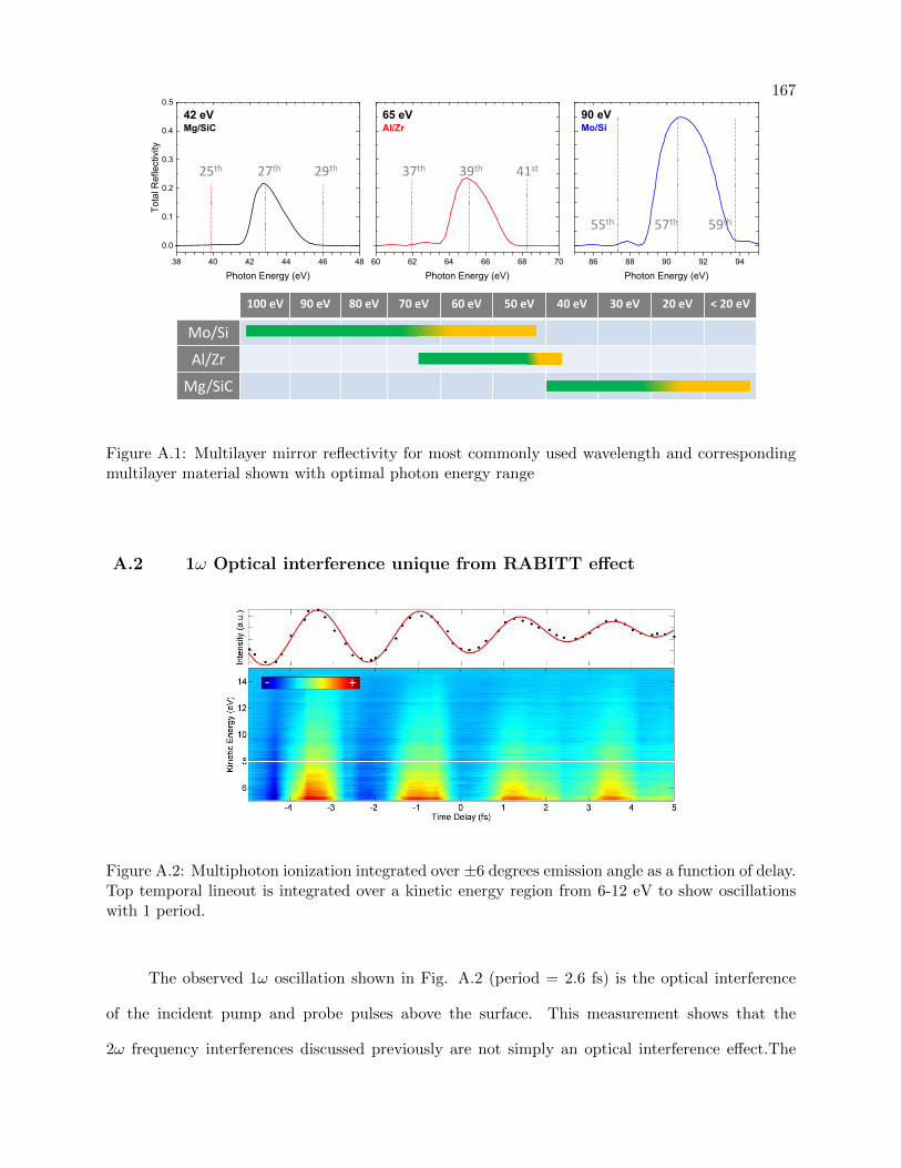
167
60 62 64 66 68 70
Photon Energy (eV)
65 eVAl/Zr
86 88 90 92 94
Photon Energy (eV)
90 eVMo/Si
38 40 42 44 46 48
0.0
0.1
0.2
0.3
0.4
0.5
Tota
l Ref
lect
ivity
Photon Energy (eV)
42 eVMg/SiC
100 eV 90 eV 80 eV 70 eV 60 eV 50 eV 40 eV 30 eV 20 eV < 20 eV
Mo/Si
Al/Zr
Mg/SiC
25th 27th 29th 37th 39th 41st
55th 57th 59th
Figure A.1: Multilayer mirror reflectivity for most commonly used wavelength and correspondingmultilayer material shown with optimal photon energy range
A.2 1ω Optical interference unique from RABITT effect
+‐
Figure A.2: Multiphoton ionization integrated over ±6 degrees emission angle as a function of delay.Top temporal lineout is integrated over a kinetic energy region from 6-12 eV to show oscillationswith 1 period.
The observed 1ω oscillation shown in Fig. A.2 (period = 2.6 fs) is the optical interference
of the incident pump and probe pulses above the surface. This measurement shows that the
2ω frequency interferences discussed previously are not simply an optical interference effect.The
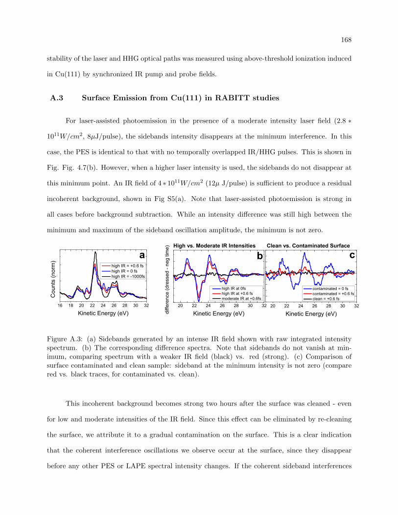
168
stability of the laser and HHG optical paths was measured using above-threshold ionization induced
in Cu(111) by synchronized IR pump and probe fields.
A.3 Surface Emission from Cu(111) in RABITT studies
For laser-assisted photoemission in the presence of a moderate intensity laser field (2.8 ∗
1011W/cm2, 8µJ/pulse), the sidebands intensity disappears at the minimum interference. In this
case, the PES is identical to that with no temporally overlapped IR/HHG pulses. This is shown in
Fig. Fig. 4.7(b). However, when a higher laser intensity is used, the sidebands do not disappear at
this minimum point. An IR field of 4 ∗ 1011W/cm2 (12µ J/pulse) is sufficient to produce a residual
incoherent background, shown in Fig S5(a). Note that laser-assisted photoemission is strong in
all cases before background subtraction. While an intensity difference was still high between the
minimum and maximum of the sideband oscillation amplitude, the minimum is not zero.
20 22 24 26 28 30 3220 22 24 26 28 30 3216 18 20 22 24 26 28 30 32
Kinetic Energy (eV)
contaminated = 0 fs contaminated = +0.6 fs clean = +0.6 fs
Clean vs. Contaminated Surface
cb
Kinetic Energy (eV)diffe
renc
e (d
ress
ed -
neg
time)
high IR at 0fs high IR at +0.6 fs moderate IR at +0.6fs
aHigh vs. Moderate IR Intensities
Cou
nts
(nor
m)
Kinetic Energy (eV)
high IR = +0.6 fs high IR = 0 fs high IR = -1000fs
Figure A.3: (a) Sidebands generated by an intense IR field shown with raw integrated intensityspectrum. (b) The corresponding difference spectra. Note that sidebands do not vanish at min-imum, comparing spectrum with a weaker IR field (black) vs. red (strong). (c) Comparison ofsurface contaminated and clean sample: sideband at the minimum intensity is not zero (comparered vs. black traces, for contaminated vs. clean).
This incoherent background becomes strong two hours after the surface was cleaned - even
for low and moderate intensities of the IR field. Since this effect can be eliminated by re-cleaning
the surface, we attribute it to a gradual contamination on the surface. This is a clear indication
that the coherent interference oscillations we observe occur at the surface, since they disappear
before any other PES or LAPE spectral intensity changes. If the coherent sideband interferences
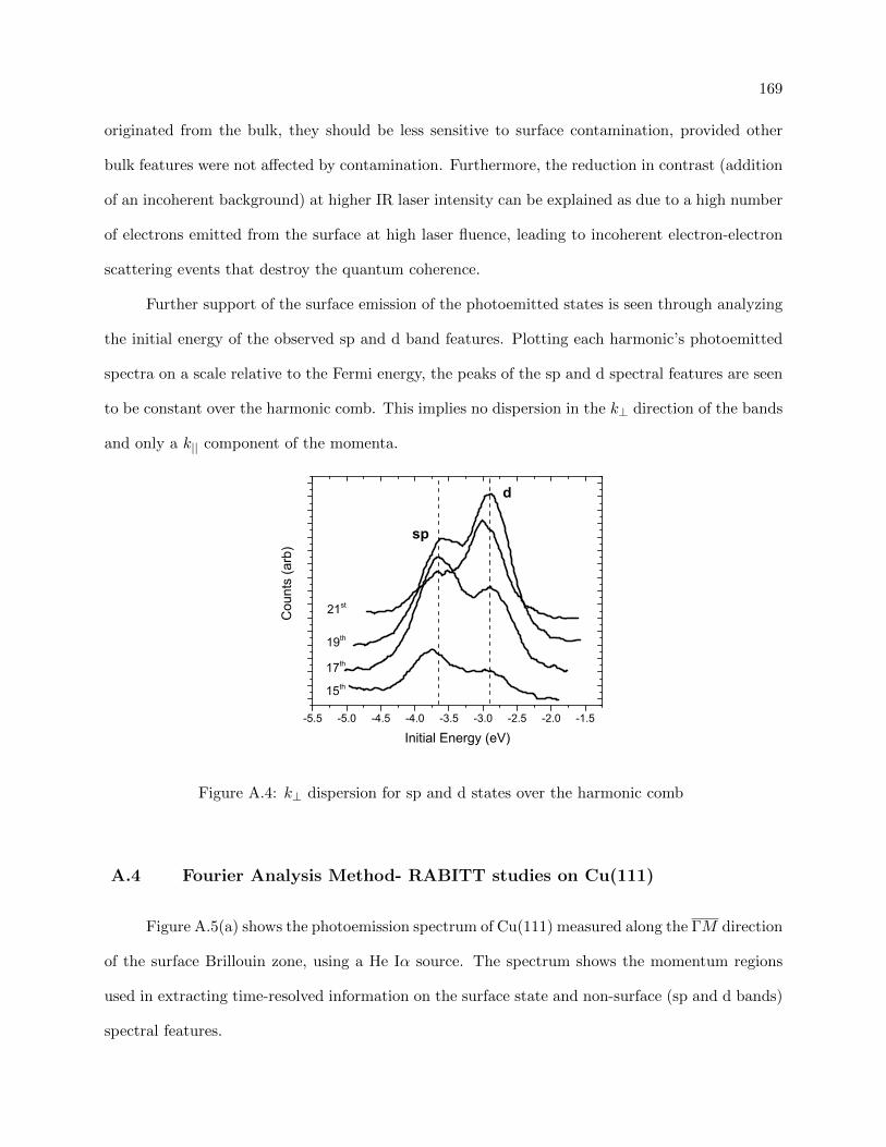
169
originated from the bulk, they should be less sensitive to surface contamination, provided other
bulk features were not affected by contamination. Furthermore, the reduction in contrast (addition
of an incoherent background) at higher IR laser intensity can be explained as due to a high number
of electrons emitted from the surface at high laser fluence, leading to incoherent electron-electron
scattering events that destroy the quantum coherence.
Further support of the surface emission of the photoemitted states is seen through analyzing
the initial energy of the observed sp and d band features. Plotting each harmonic’s photoemitted
spectra on a scale relative to the Fermi energy, the peaks of the sp and d spectral features are seen
to be constant over the harmonic comb. This implies no dispersion in the k⊥ direction of the bands
and only a k|| component of the momenta.
-5.5 -5.0 -4.5 -4.0 -3.5 -3.0 -2.5 -2.0 -1.5
d
19th
21st
17th
Cou
nts
(arb
)
Initial Energy (eV)
15th
sp
Figure A.4: k⊥ dispersion for sp and d states over the harmonic comb
A.4 Fourier Analysis Method- RABITT studies on Cu(111)
Figure A.5(a) shows the photoemission spectrum of Cu(111) measured along the ΓM direction
of the surface Brillouin zone, using a He Iα source. The spectrum shows the momentum regions
used in extracting time-resolved information on the surface state and non-surface (sp and d bands)
spectral features.
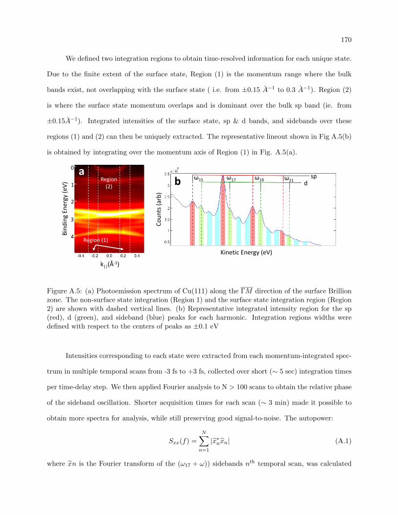
170
We defined two integration regions to obtain time-resolved information for each unique state.
Due to the finite extent of the surface state, Region (1) is the momentum range where the bulk
bands exist, not overlapping with the surface state ( i.e. from ±0.15 A−1 to 0.3 A−1). Region (2)
is where the surface state momentum overlaps and is dominant over the bulk sp band (ie. from
±0.15A−1). Integrated intensities of the surface state, sp & d bands, and sidebands over these
regions (1) and (2) can then be uniquely extracted. The representative lineout shown in Fig A.5(b)
is obtained by integrating over the momentum axis of Region (1) in Fig. A.5(a).
k||(Å‐1)
Bind
ing Energy (e
V)
0
1
2
3
4 Region (1)
Region(2)
ab
Coun
ts (arb)
Kinetic Energy (eV)
ω15 ω17 ω19 ω21 dsp
Figure A.5: (a) Photoemission spectrum of Cu(111) along the ΓM direction of the surface Brillionzone. The non-surface state integration (Region 1) and the surface state integration region (Region2) are shown with dashed vertical lines. (b) Representative integrated intensity region for the sp(red), d (green), and sideband (blue) peaks for each harmonic. Integration regions widths weredefined with respect to the centers of peaks as ±0.1 eV
Intensities corresponding to each state were extracted from each momentum-integrated spec-
trum in multiple temporal scans from -3 fs to +3 fs, collected over short (∼ 5 sec) integration times
per time-delay step. We then applied Fourier analysis to N > 100 scans to obtain the relative phase
of the sideband oscillation. Shorter acquisition times for each scan (∼ 3 min) made it possible to
obtain more spectra for analysis, while still preserving good signal-to-noise. The autopower:
Sxx(f) =N∑n=1
|x∗nxn| (A.1)
where xn is the Fourier transform of the (ω17 + ω)) sidebands nth temporal scan, was calculated
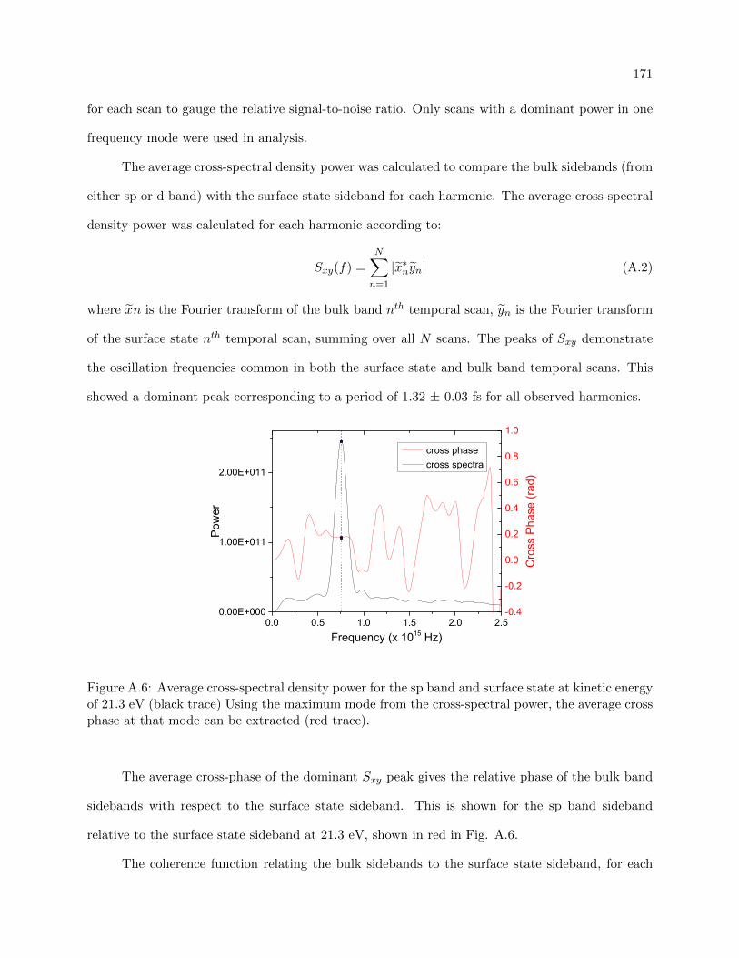
171
for each scan to gauge the relative signal-to-noise ratio. Only scans with a dominant power in one
frequency mode were used in analysis.
The average cross-spectral density power was calculated to compare the bulk sidebands (from
either sp or d band) with the surface state sideband for each harmonic. The average cross-spectral
density power was calculated for each harmonic according to:
Sxy(f) =
N∑n=1
|x∗nyn| (A.2)
where xn is the Fourier transform of the bulk band nth temporal scan, yn is the Fourier transform
of the surface state nth temporal scan, summing over all N scans. The peaks of Sxy demonstrate
the oscillation frequencies common in both the surface state and bulk band temporal scans. This
showed a dominant peak corresponding to a period of 1.32 ± 0.03 fs for all observed harmonics.
0.0 0.5 1.0 1.5 2.0 2.5-0.4
-0.2
0.0
0.2
0.4
0.6
0.8
1.0
cross phase
Cro
ss P
hase
(rad
)
Frequency (x 1015 Hz)
0.00E+000
1.00E+011
2.00E+011 cross spectra
Pow
er
Figure A.6: Average cross-spectral density power for the sp band and surface state at kinetic energyof 21.3 eV (black trace) Using the maximum mode from the cross-spectral power, the average crossphase at that mode can be extracted (red trace).
The average cross-phase of the dominant Sxy peak gives the relative phase of the bulk band
sidebands with respect to the surface state sideband. This is shown for the sp band sideband
relative to the surface state sideband at 21.3 eV, shown in red in Fig. A.6.
The coherence function relating the bulk sidebands to the surface state sideband, for each
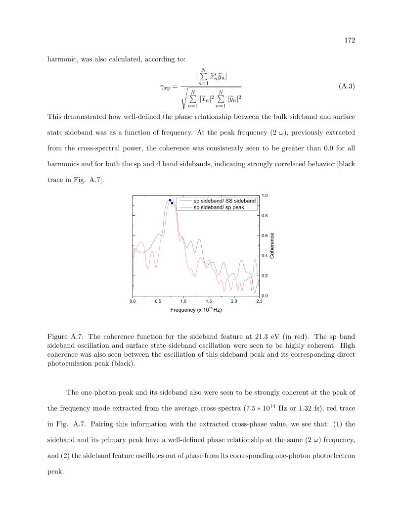
172
harmonic, was also calculated, according to:
γxy =
|N∑n=1
x∗nyn|√N∑n=1|xn|2
N∑n=1|yn|2
(A.3)
This demonstrated how well-defined the phase relationship between the bulk sideband and surface
state sideband was as a function of frequency. At the peak frequency (2 ω), previously extracted
from the cross-spectral power, the coherence was consistently seen to be greater than 0.9 for all
harmonics and for both the sp and d band sidebands, indicating strongly correlated behavior [black
trace in Fig. A.7].
0.0 0.5 1.0 1.5 2.0 2.50.0
0.2
0.4
0.6
0.8
1.0
Coh
eren
ce
Frequency (x 1015 Hz)
sp sideband/ SS sideband sp sideband/ sp peak
Figure A.7: The coherence function for the sideband feature at 21.3 eV (in red). The sp bandsideband oscillation and surface state sideband oscillation were seen to be highly coherent. Highcoherence was also seen between the oscillation of this sideband peak and its corresponding directphotoemission peak (black).
The one-photon peak and its sideband also were seen to be strongly coherent at the peak of
the frequency mode extracted from the average cross-spectra (7.5 ∗ 1014 Hz or 1.32 fs), red trace
in Fig. A.7. Pairing this information with the extracted cross-phase value, we see that: (1) the
sideband and its primary peak have a well-defined phase relationship at the same (2 ω) frequency,
and (2) the sideband feature oscillates out of phase from its corresponding one-photon photoelectron
peak.
173
For each harmonic, the coherence value was used in calculating the final error on the extracted
cross-phase between the bulk and surface state sidebands. This was calculated from:
εγ =
√(1− γxy(fmax)
γxy(fmax)∗2N1/2 (A.4)
where fmax is the frequency of the maximum in the cross-spectral power, as indicated by the blue
markers in figure A.6, and N is the total number of scans. This gives the error values quoted in
Fig. 4.8.
A.5 Details of DFT and Bader Charge Analysis for Na intercalation on
Gr/Ni(111)
All calculations for the results presented in Section 5.6.2.3 were performed using the VASP
code [312] based on spin-polarized density functional theory (DFT). The projector augmented wave
potentials were used for electron-ion interactions [313, 314]. Van der Waals dispersion forces were
accounted for through the optB88-vdW functional by using the vdW-DF approach [315, 316, 317].
The 2p electrons of Na were explicitly treated as valence electrons by using the semi-core potential
and the electron wave function was expanded using plane waves with an energy cutoff of 400 eV.
The Ni(111) surface was modeled by a six layer slab separated from its periodic image in z-direction
by a vacuum of at least 13 A. The graphene was adsorbed on the Ni(111) surface by applying the
commensurate condition. A (1x1) primitive cell in the top-fcc configuration (one carbon atop of
Ni and the other carbon above the fcc hollow site, as shown in Fig 5.6a) was used to model the
graphene/Ni(111) system.
To model the Na adsorption on top of graphene/Ni(111) or after intercalation, a single Na
atom was adsorbed on top of graphene or was intercalated between graphene and Ni(111) in (3x3)
and (2x2) surface unit cells, corresponding to a Na coverage of 1 ML and 0.75 ML, respectively. The
Brillouin zones of (1x1), (3x3), and (2x2) were sampled using (17x17x1), (11x11x1), and (9x9x1)
Monkhorst-Pack k-point mesh [318], respectively. The three bottom-most Ni(111) layers were fixed
during relaxation. All structures were fully relaxed until the Hellmann-Feynman forces acting on

174
the atoms were smaller than 0.01 eV/A. The dipole correction was included and the electrostatic
potential was adjusted accordingly [318]. To investigate the effect of Na adsorption and intercalation
on the graphene states, the band structures of the Na/Gr/Ni(111) and Gr/Na/Ni(111) systems (as
shown in Fig 5.13) were calculated in a larger (2x2) supercell. This made it possible to compare
the experimental ARPES data with the calculated band structures without unfolding the band
structures of the supercell.