ultracompact si slot waveguidebased polarization rotators
TRANSCRIPT
antenna at 2.4 GHz and this frequency the loop is caused an
omni directional pattern at antenna. But at higher frequency, the
inductance effect of the CRLH cells are reduced so the maxi-
mum current distribution are concentrated CRLH capacitances.
Therefore, in this condition we cannot see that effective current
loop, so directive pattern is predictable and according to Figure
6(g) the antenna pattern shows directive characteristic.
4. CONCLUSION
This article shows the effect of CRLH cells on designing dual
band antenna base on Zeroth-order resonance. Here, two differ-
ent form of CRLH antenna with corner ground is presented with
two different radiation pattern the first antenna has omnidirec-
tional radiation and second antenna shows omnidirectional pat-
tern at lower frequency and semidirectional pattern for higher
frequency with more bandwidth. First antenna, has two resonan-
ces at 1.85 and 5. 5 GHz for GSM 1800 and 5.2 GHz WLAN
indoor application. In the second antenna, first band support
2.38–2.48 GHz that covers the WLAN. The second operation
band is between 4.18 and 9.85 GHz for covering WLAN. The
current distribution shows that how these CRLH cells are helped
for change in pattern of antenna and frequencies effects on
inductance and capacitance of the CRLH shows in current dis-
pense. As shows in this article, the CRLH cells are shaped the
current as a loop in antenna surface and this current loop is
affected on antenna radiation pattern and making a omnidirec-
tional pattern. Most of the simulation result are compared with
measured experimental result for check the truth of result.
REFERENCES
1. F.B. Zarrabi, A.M. Shire, M. Rahimi, and N.P. Gandji, Ultra-wide-
band tapered patch antenna with fractal slots for dual notch applica-
tion, Microwave Opt Technol Lett 56 (2014), 1344–1348.
2. T.M. Telsang and A.B. Kakade, Ultrawideband slotted semicircular
patch antenna, Microwave Opt Technol Lett 56 (2014), 362–369.
3. D. Gibbins, M. Klemm, I.J. Craddock, J.A. Leendertz, A. Preece,
and R. Benjamin, A comparison of a wide-slot and a stacked patch
antenna for the purpose of breast cancer detection, IEEE Trans
Antennas Propag 58 (2010), 665–674.
4. B. Boroomandisorkhabi, R.A. Sadeghzadeh, F.B. Zarrabi, and E.
Ghahramani, A novel UWB circular CPW antenna with triple notch
band characteristics, In: Antennas and Propagation Conference
(LAPC), Loughborough, 2013, pp. 637–640.
5. F.B. Zarrabi, S. Sharma, Z. Mansouri, and F. Geran, Triple band
microstrip slot antenna for WIMAX/WLAN applications with SRR
Shape Ring. In: Fourth International Conference on Advanced Com-
puting & Communication Technologies (ACCT), 2014, pp. 368–371.
6. M. Rahimi, F.B. Zarrabi, R. Ahmadian, Z. Mansouri, and A.
Keshtkar, Miniaturization of antenna for wireless application with
difference metamaterial structures, Prog Electromagnet Res 145
(2014), 19–29.
7. H. Kim, J.-H. Park, and J.-H. Lee, Composite right/left-handed-
coupled line bandpass filter using the first negative resonant mode,
Microwave Opt Technol Lett 53 (2011), 943–947.
8. Y.-H. Ryu, J.-h. Park, J.-H. Lee, and H.-S. Tae, Generalized
negative-refractive index transmission line based on defected ground
structure, Microwave Opt Technol Lett 52 (2010), 2223–2225.
9. Y.-H. Ryu, J.-h. Park, J.-H. Lee, and H.-S. Tae. Multiband antenna
using1 1,2 1, and 0 resonant mode of DGS dual composite right/
left handed transmission line. Microwave Opt Technol Lett 51
(2009), 2485–2488.
10. M. Rahimi, R.A. Sadeghzadeh, F.B. Zarrabi, and Z. Mansouri,
Band-notched UWB monopole antenna design with novel feed for
taper rectangular radiating patch, Prog Electromagnet Res C 47
(2014), 147–155.
11. X. Luo, J.-G. Ma, K. S. Yeo, and E.-P. Li. Compact ultra-wideband
(UWB) bandpass filter with ultra-narrow dual-and quad-notched
bands. IEEE Trans Microwave Theory Tech 59 (2011), 1509–1519.
12. J. Liang, L. Guo, C.C. Chiau, X. Chen and C.G. Parini, Study of
CPW-fed circular disc monopole antenna for ultra wideband applica-
tions, IEE Microwave Antennas Propag (2005), 520–526.
13. J. Liu, S. Zhong, and K.P. Esselle, A printed elliptical monopole
antenna with modified feeding structure for bandwidth enhancement,
IEEE Trans Antennas Propag 59 (2011), 667–670.
14. E. Antonino-Daviu, M. Fabres, M. Ferrando-Bataller, and V. M. R.
Pe~narrocha, Modal analysis and design of band-notched UWB planar
monopole antennas, IEEE Trans Antennas Propag 58 (2010), 1457–
1467.
15. N. Ojaroudi, M. Ojaroudi, and K. Halili, Design of triple-band
monopole antenna with meander line structure for MIMO applica-
tion, Microwave Opt Technol Lett 54 (2012), 2168–2172.
16. M. Naser-Moghadasi and L. Asadpor, Improved band-notch techni-
ques for miniature UWB CPW-fed slot antenna, Microwave Opt
Technol Lett 56 (2014), 408–415.
17. Y.D. Dong, W. Hong, Z.Q. Kuai, C. Yu, Y. Zhang, J.Y. Zhou, and
J.-X. Chen, Development of ultrawideband antenna with multiple
band-notched characteristics using half mode substrate integrated
waveguide cavity technology, IEEE Trans Antennas Propag 56
(2008), 2894–2902.
18. X.-C. Yin, C.-L. Ruan, C.-Y. Ding, and J.-H. Chu, A compact ultra-
wideband microstrip antenna with multiple notches, Prog Electro-
magnet Res 84 (2008), 321–332.
19. D.-B. Lin, I. Tang, and Y.-J. Wei, Compact dual-band-notched
CPW-fed wide-slot antenna for WLAN and WiMAX applications,
Microwave Opt Technol Lett 53 (2011), 1496–1501.
20. M. Naser-Moghadasi, R.A. Sadeghzadeh-Sheikhan, T. Sedghi, T.
Aribi, and B. S. Virdee, UWB CPW-fed fractal patch antenna with
band-notched function employing folded T-shaped element. IEEE
Antennas Wireless Propag Lett 12 (2013), 504–507.
21. J.H. Wang, Z. Wang, Y.-Z. Yin, and X. L. Liu, UWB monopole
antenna with triple band-notched characteristic based on a pair of
novel resonators, Prog Electromagn Res C 49 (2014), 1–10.
22. M.M.M. Ali, A.A.R. Saad, and E.E.M. Khaled. Implementation and
justification of a triple frequency-notched UWB proximity-fed antenna
with shunt stubs. Microwave Opt Technol Lett 56 (2014), 646–654.
23. J.-H. Park, Y.-H. Ryu, J.-G. Lee, and J.-H. Lee. Epsilon negative
zeroth-order resonator antenna. IEEE Trans Antennas Propag 55
(2007), 3710–3712.
24. S.A. Hosseini, Z. Atlasbaf, and K. Forooraghi, Two new loaded
compact palnar ultra-wideband antennas using defected ground struc-
tures, Prog Electromagn Res B, 2 (2008), 165–176.
25. M. Mokhtaari and J. Bornemann, Directional ultra-wideband anten-
nas in planar technologies, In: 38th European, Microwave Confer-
ence, EuMC 2008, Amsterdam, Holland, 2008, pp. 885–888.
26. M. Pramod and K.J. Vinoy, Electronically tunable zero order resona-
tor based on CRLH-TLs, In: National Conference on Communica-
tions (NCC), 2011, pp. 1–3.
VC 2015 Wiley Periodicals, Inc.
ULTRACOMPACT Si SLOT WAVEGUIDE-BASED POLARIZATION ROTATORS
Thang Q. Tran and Sangin KimDepartment of Electrical and Computer Engineering, Ajou University,Suwon 443-749, Gyeonggi Province, Korea; Corresponding author:[email protected]
Received 23 August 2014
ABSTRACT: A novel silicon asymmetric tilted slot waveguide-basedpolarization rotator is presented. A large birefringence in the silicon
slot waveguide facilitated a compact polarization rotator of
DOI 10.1002/mop MICROWAVE AND OPTICAL TECHNOLOGY LETTERS / Vol. 57, No. 4, April 2015 779
subwavelength scale. A 1287 nm long TM to TE and TE to TM polariza-
tion rotator was achieved with an extinction ratio of 10 dB and aninsertion loss of less than 5 dB at an operating wavelength of 1500 nm.Further performance improvement is possible for polarization rotator
designed to work on TM to TE (or TE to TM) conversion: a 711 nmlong TM to TE polarization rotator with 9.25 dB extinction ratio and2.2dB insertion loss was also numerically demonstrated. VC 2015 Wiley
Periodicals, Inc. Microwave Opt Technol Lett 57:779–785, 2015; View
this article online at wileyonlinelibrary.com. DOI 10.1002/mop.28953
Key words: polarization rotator; waveguide optics; silicon on insulator;slot waveguide
1. INTRODUCTION
The design of ultracompact polarization rotator is necessary for
highly integrated optical design. Nano-sized optical device
designs often require a unique polarization to function correctly.
The solution for such problem is polarization diversity, which
requires the design of an efficient and compact polarization rota-
tor for future integrated photonics. The design of an efficient
polarization rotator with low insertion loss, high extinction ratio,
and short operation length is still a difficult task.
It is acknowledged that the most difficult issue in
birefringence-based directly coupled polarization rotator is the
matching of the coupling coefficients [1]. In direct coupling Si-
based polarization rotating device, the device length is so small
that all propagation losses are negligible, and the single most
important loss is the coupling loss, resulting from the mode mis-
match between the input and output waveguide and the device.
These coupling losses are often high, and tuning such losses to
achieve good performance is often difficult. For such reason, the
majority of recent advances in polarization rotator are modal
evolution-based devices [1–3]. However, directly coupled devi-
ces, due to the lack of taper, can be made much shorter.
Besides, in the directly coupled devices, the propagating modes
can be made to be drastically different, so that a high birefrin-
gence, and thus, a further reduced device length are obtained.
There are recent advances in hybrid plasmon-based polarization
rotators [4–8], however, the device that offers an ultrashort
device length at a reasonably low insertion loss is still out of
reach. The best device so far achieved rotation at a device
length of 3.2 lm and an insertion loss of �1.38 dB [8]. In [5], a
TM to TE polarization rotator was designed at 3 lm long and
11 dB extinction ratio, but with very high insertion loss of 10
dB. In [6], loss compensator is required, in [9], nonlinear mate-
rial is needed, and the device length is relatively long (�6 lm).
In [10], very short conversion length was achieved. However,
due to very large coupling waveguide width of approximately 5
lm, single-mode operation of the output waveguide cannot be
guaranteed, which can be an obstacle to integration with other
devices and require an additional taper structure. In [11], a 3
lm device and a 4.8 lm tapered design were realized, however,
subwavelength conversion length was not obtained. Similarly, a
hybrid plasmonic waveguides design was presented in [8],
achieved a device length of 3.2 lm and an insertion loss of
�1.38 dB. However, as far as we know, no work in literature
has achieved yet a sub wavelength scale device length.
In this work, we propose a polarization rotator based on a
silicon-air slot waveguide with single-mode input/output wave-
guides. The silicon-air slot waveguide shows a giant optical
birefringence between the slot mode and the dielectric mode
mainly due to the large different of permittivity between Si and
air. A directly coupled polarization rotator design based on a
slanted dielectric slot waveguide, to our best knowledge, has not
been carried out. The design based on traditional silicon tech-
nology further adds to the attractiveness of the device. We have
shown that a 1287 nm long TM to TE and TE to TM simultane-
ous polarization rotator and a 711 nm long polarization rotator
optimized for TM to TE operation can be realized at
k 5 1500 nm.
2. OPERATION PRINCIPLE AND DESIGN CONSTRAINTS
For a birefringence-based polarization rotator with index differ-
ence of Dn, the optimal device length will be L5k=ð2DnÞ,where k is an operating wavelength. Generally, the larger the
index difference Dn is, the shorter the device length, thus more
desirable. Slot waveguide-based polarization rotators are espe-
cially promising as a slot mode exists only for a certain polar-
ization with electric field normal to the Si-air interface, which is
usually referred to as TM polarization, and has much lower
effective index than dielectric modes.
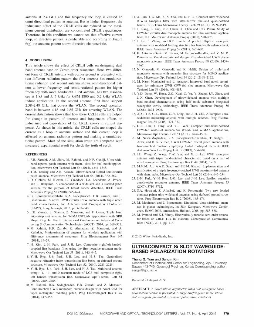
Figure 1 shows the proposed structure, where the polarization
rotating part consists of a slant slot waveguide on SiO2 and two
identical single-mode waveguides are adopted as input and out-
put waveguides. In this work, the single-mode waveguide is
designed to support only the lowest order mode for each polar-
ization, so that no additional taper structure is needed for inte-
gration with other waveguide-based devices. In the slant slot
Figure 1 (a) 3D structure of the polarization rotating device. The device consists of a inclined Si slot waveguide, represented in yellow, with an input
and an output Si waveguide, represented in green color. The substrate, represented in dark green, is SiO2. (b) Five design parameters of the polarization
rotating device: the height of the device (H), width of the foundation of the device (D), the slot width (DS), the rotating angle (h), and the width of the
input and output rib waveguide (not shown, identical by design). The height of the input and output waveguide was selected to be identical to the device
height H for ease of fabrication purposes. Both figures are to scale to the optimized version of the device, with H 5 360 nm, D 5 865 nm, DS 5 180 nm,
h 5 56.24�, and the input waveguide width is 400 nm. The device’s length is L 5 1287 nm. [Color figure can be viewed in the online issue, which is
available at wileyonlinelibrary.com]
780 MICROWAVE AND OPTICAL TECHNOLOGY LETTERS / Vol. 57, No. 4, April 2015 DOI 10.1002/mop
waveguide, it is desired that only two guided modes exist: one
is a slot mode of a low effective index with electric field normal
to the Si-air interface and the other is a dielectric mode of a
high effective index with electric field parallel to the Si-air
interface.
When the slant slot waveguide supports only two modes
referred to as low- and high-index modes (LIM and HIM), an
operation principle of the polarization rotator is described in
Figure 2. At the interface between the input/output waveguide
and the slant slot waveguide, light from input waveguide of TE
or TM polarization is coupled to both HIM and LIM of the slant
slot waveguide. Those two modes experience different phase
retardations and each of those two modes is coupled to both TE
and TM polarization modes of the output waveguide.
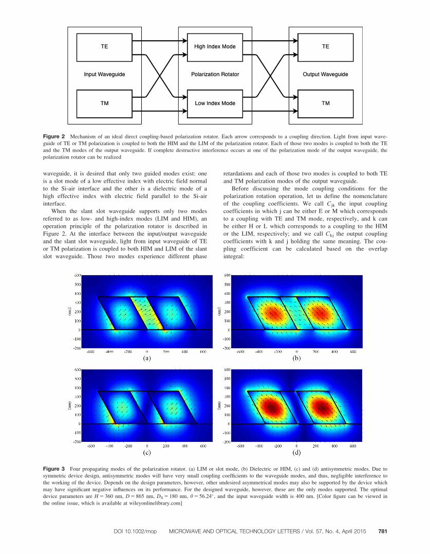
Before discussing the mode coupling conditions for the
polarization rotation operation, let us define the nomenclature
of the coupling coefficients. We call Cjk the input coupling
coefficients in which j can be either E or M which corresponds
to a coupling with TE and TM mode, respectively, and k can
be either H or L which corresponds to a coupling to the HIM
or the LIM, respectively; and we call Ckj the output coupling
coefficients with k and j holding the same meaning. The cou-
pling coefficient can be calculated based on the overlap
integral:
Figure 2 Mechanism of an ideal direct coupling-based polarization rotator. Each arrow corresponds to a coupling direction. Light from input wave-
guide of TE or TM polarization is coupled to both the HIM and the LIM of the polarization rotator. Each of those two modes is coupled to both the TE
and the TM modes of the output waveguide. If complete destructive interference occurs at one of the polarization mode of the output waveguide, the
polarization rotator can be realized
Figure 3 Four propagating modes of the polarization rotator. (a) LIM or slot mode, (b) Dielectric or HIM, (c) and (d) antisymmetric modes. Due to
symmetric device design, antisymmetric modes will have very small coupling coefficients to the waveguide modes, and thus, negligible interference to
the working of the device. Depends on the design parameters, however, other undesired asymmetrical modes may also be supported by the device which
may have significant negative influences on its performance. For the designed waveguide, however, these are the only modes supported. The optimal
device parameters are H 5 360 nm, D 5 865 nm, DS 5 180 nm, h 5 56.24�, and the input waveguide width is 400 nm. [Color figure can be viewed in
the online issue, which is available at wileyonlinelibrary.com]
DOI 10.1002/mop MICROWAVE AND OPTICAL TECHNOLOGY LETTERS / Vol. 57, No. 4, April 2015 781
C5jÐ Ð
E1�E2dAj2Ð Ð
jE1j2dAÐ ÐjE2j2dA
; (1)
where E1 and E2 are vector fields of the corresponding modes
in the input waveguide and the slant slot waveguide, respec-
tively. As the input and output waveguides are identical, which
has an added benefit of simplifying design, Cjk 5 Ckj is
satisfied.
If TE polarized light is assumed to be launched through the
input waveguide, there are four optical paths which can be
taken by light: TE-HIM-TE, TE-LIM-TE, TE-HIM-TM, and
TE-LIM-TM. Due to the different in effective indices between
the HIM and the LIM, there will be phase differences among
the optical paths. If the slant slot waveguide length is deter-
mined such that the phase retardation difference between the
HIM and the LIM is p, the TE-HIM-TE and the TE-LIM-TE
paths will be completely out of phase, and the TE-HIM-TM
and the TE-LIM-TM will be completely in-phase. To have a
complete destructive interference between TE-HIM-TE and
TE-LIM-TE at the output waveguide, they need to have
the same amplitude, that is, CEH*CHE 5 CEL*CLE. As
CEH 5 CHE and CEL 5 CLE, the additional condition for TE-to-
TM polarization rotation becomes CEH 5 CEL. The output
amplitude of TM polarization in such case would be
(CEH*CHM 1 CEL*CLM). Similar reasoning can be said for a
TM polarized input, which results in an amplitude matching
condition of CMH 5 CML and an rotated output amplitude of
(CMH*CHE 1 CML*CLE).
An important consequence of the foregoing is that the TE to
TM conversion condition (CMH 5 CML) and the TM to TE con-
version condition (CEH 5 CEL) can be achieved independently.
This implies that the interference-based device does not neces-
sary offer simultaneous TE to TM and TM to TE rotations. By
satisfying only one of the polarization rotation conditions, one
can potentially realize a polarization rotator with better perform-
ance in some specific applications where a simultaneous polar-
ization rotator device is not required.
3. DEVICE DESIGN AND ANALYSIS
Designing the device involves optimizing five parameters
including those four geometrical parameters presented in Figure
1(b) and the width of the input/output waveguide. The guided
modes in the slant slot waveguide and the input/output wave-
guide are calculated using the finite element method, and the
corresponding coupling coefficients are calculated based on the
field profiles of the modes. From the calculated effective index
difference between the HIM and the LIM, the device length can
be estimated. By repeating this process with those five geometri-
cal parameters varied, we should find an optimum set of the
parameters satisfying the polarization conversion condition. This
optimization process is extremely time-consuming. In this work,
we focused on minimization of the device length with an
acceptable insertion loss in the parameter optimization process.
Figure 4 FEM calculated coupling coefficients CEL, CEH, CML, and CMH, versus different input waveguide width, with different slant angle h. The
rest of the parameters, which are the same for the four cases, are H 5 865 nm, D 5 360 nm, DS 5 180 nm. [Color figure can be viewed in the online
issue, which is available at wileyonlinelibrary.com]
782 MICROWAVE AND OPTICAL TECHNOLOGY LETTERS / Vol. 57, No. 4, April 2015 DOI 10.1002/mop
There appeared to be a tradeoff between the insertion loss of
the device and the device length. A larger slot size will increase
its modal area, thus increase its coupling coefficient and reduce
the insertion loss. However, the larger slot size will reduce the
effective index of the dielectric mode and thus, Dn, which con-
sequently results in an increase of the device length. In the
design of the slant slot waveguide, it should also be considered
to prevent the appearance of higher-order asymmetrical modes.
Due to the sharp edges and intrinsic asymmetrical properties of
the polarization rotator, multiple nondesired propagating modes
may exist within the polarization rotator. An unintended cou-
pling of the input light to the undesired higher-order modes will
have a detrimental effect to the performance reducing the
extinction rate of the polarization rotator. To suppress those
higher-order modes, the slant slot waveguide should be made
small enough. However, if the device is small enough to prevent
the unwanted modes, the existence of the HIM and the LIM is
not guaranteed. Moreover, reducing the transverse dimension of
the device will reduce the coupling efficiency to the input/output
waveguides. Therefore, the transverse dimension of the device is
designed so as to allow up to the second order antisymmetric
modes. If the single-mode input/output waveguide is adopted,
the excitation of the antisymmetric modes will be negligible
bringing about an order of magnitude lower coupling coeffi-
cients compared to the HIM and the LIM, thus, will not seri-
ously interfere with the operation of the polarization rotator.
From our investigation, it has been found that H> 200 nm is
required to support the LIM and to keep the excitation of the
antisymmetric modes low enough H< 420 nm is needed. Figure
3 represent all the guided modes of the slant slot waveguide of
H 5 360 nm, D 5 865 nm, Ds 5 180 nm, and h 5 56.24�, which
is close to the optimal structure. The HIM have the effective
index nHi 5 2.4797, and the LIM have the effective index
nLo 5 1.8966, thus, the index different Dn is 0.5831, which cor-
responds to a device length of � 1287 nm at k 5 1500 nm. Fig-
ures 3(a) and 3(b) show the HIM and the LIM, respectively.
Their related antisymmetric modes are represented in Figures
3(c) and 3(d), respectively.
From our extensive investigation, it has been found that the
slant angle, h does not seriously affect the existence of the
guided modes and Dn of the slant slot waveguide and instead,
dramatically change the coupling coefficients to the input/output
waveguide. So, we could achieve the satisfactory optimization
run by scanning of the input waveguide width with different
angle h while keeping the rest of the geometrical parameters
constant, which is represented in Figure 4. This is just one of
many scans performed; extensive runs at different H, D, and Ds
were also performed, but due to the limitation of the pages they
are not presented. To maximize the coupling efficiency and
make the device fabrication simple, the height of the input/out-
put waveguide was chosen to be the same as D. For
D 5 360 nm, single-mode operation of the input/output
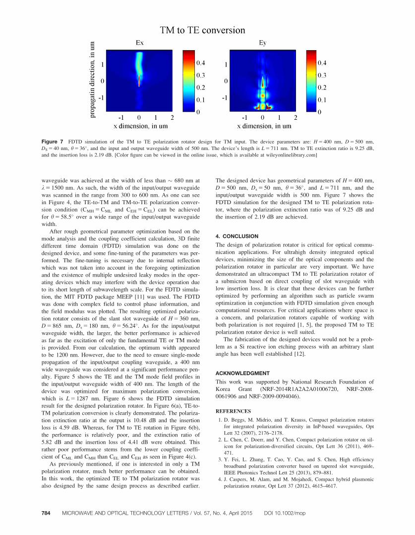
Figure 6 FDTD simulation of the simultaneous polarization rotator design for (a) TE to TM conversion and (b) TM to TE conversion. Simulation was
done in complex, and color represent the field modulus to filter out the effect of phase. The device parameters are H 5 360 nm, D 5 865 nm,
DS 5 180 nm, h 5 56.24�, and the input waveguide width is 400 nm. The device’s length is L 5 1287 nm. The extinction ratio for TE to TM is 10.48 dB
with an insertion loss of 4.59 dB. For TM to TE rotation, the extinction ratio is 5.82 dB and the insertion loss is 4.41 dB. [Color figure can be viewed
in the online issue, which is available at wileyonlinelibrary.com]
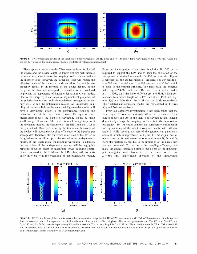
Figure 5 Two propagating modes of the input and output waveguides, (a) TE mode and (b) TM mode. Input waveguide width is 400 nm. [Color fig-
ure can be viewed in the online issue, which is available at wileyonlinelibrary.com]
DOI 10.1002/mop MICROWAVE AND OPTICAL TECHNOLOGY LETTERS / Vol. 57, No. 4, April 2015 783
waveguide was achieved at the width of less than � 680 nm at
k 5 1500 nm. As such, the width of the input/output waveguide
was scanned in the range from 300 to 600 nm. As one can see
in Figure 4, the TE-to-TM and TM-to-TE polarization conver-
sion condition (CMH 5 CML and CEH 5 CEL) can be achieved
for h 5 58.5� over a wide range of the input/output waveguide
width.
After rough geometrical parameter optimization based on the
mode analysis and the coupling coefficient calculation, 3D finite
different time domain (FDTD) simulation was done on the
designed device, and some fine-tuning of the parameters was per-
formed. The fine-tuning is necessary due to internal reflection
which was not taken into account in the foregoing optimization
and the existence of multiple undesired leaky modes in the oper-
ating devices which may interfere with the device operation due
to its short length of subwavelength scale. For the FDTD simula-
tion, the MIT FDTD package MEEP [11] was used. The FDTD
was done with complex field to control phase information, and
the field modulus was plotted. The resulting optimized polariza-
tion rotator consists of the slant slot waveguide of H 5 360 nm,
D 5 865 nm, Ds 5 180 nm, h 5 56.24�. As for the input/output
waveguide width, the larger, the better performance is achieved
as far as the excitation of only the fundamental TE or TM mode
is provided. From our calculation, the optimum width appeared
to be 1200 nm. However, due to the need to ensure single-mode
propagation of the input/output coupling waveguide, a 400 nm
wide waveguide was considered at a significant performance pen-
alty. Figure 5 shows the TE and the TM mode field profiles in
the input/output waveguide width of 400 nm. The length of the
device was optimized for maximum polarization conversion,
which is L 5 1287 nm. Figure 6 shows the FDTD simulation
result for the designed polarization rotator. In Figure 6(a), TE-to-
TM polarization conversion is clearly demonstrated. The polariza-
tion extinction ratio at the output is 10.48 dB and the insertion
loss is 4.59 dB. Whereas, for TM to TE rotation in Figure 6(b),
the performance is relatively poor, and the extinction ratio of
5.82 dB and the insertion loss of 4.41 dB were obtained. This
rather poor performance stems from the lower coupling coeffi-
cient of CML and CMH than CEL and CEH as seen in Figure 4(c).
As previously mentioned, if one is interested in only a TM
polarization rotator, much better performance can be obtained.
In this work, the optimized TE to TM polarization rotator was
also designed by the same design process as described earlier.
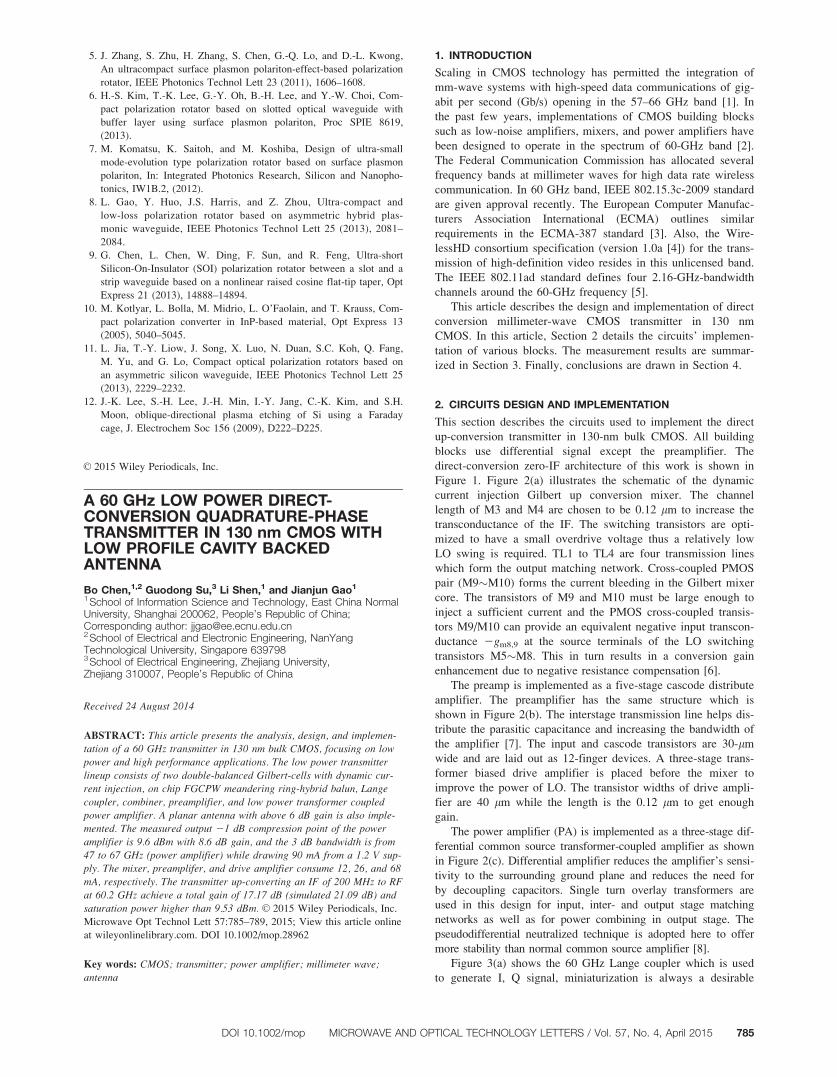
The designed device has geometrical parameters of H 5 400 nm,
D 5 500 nm, Ds 5 50 nm, h 5 36�, and L 5 711 nm, and the
input/output waveguide width is 500 nm. Figure 7 shows the
FDTD simulation for the designed TM to TE polarization rota-
tor, where the polarization extinction ratio was of 9.25 dB and
the insertion of 2.19 dB are achieved.
4. CONCLUSION
The design of polarization rotator is critical for optical commu-
nication applications. For ultrahigh density integrated optical
devices, minimizing the size of the optical components and the
polarization rotator in particular are very important. We have
demonstrated an ultracompact TM to TE polarization rotator of
a submicron based on direct coupling of slot waveguide with
low insertion loss. It is clear that these devices can be further
optimized by performing an algorithm such as particle swarm
optimization in conjunction with FDTD simulation given enough
computational resources. For critical applications where space is
a concern, and polarization rotators capable of working with
both polarization is not required [1, 5], the proposed TM to TE
polarization rotator device is well suited.
The fabrication of the designed devices would not be a prob-
lem as a Si reactive ion etching process with an arbitrary slant
angle has been well established [12].
ACKNOWLEDGMENT
This work was supported by National Research Foundation of
Korea Grant (NRF-2014R1A2A2A01006720, NRF-2008-
0061906 and NRF-2009-0094046).
REFERENCES
1. D. Beggs, M. Midrio, and T. Krauss, Compact polarization rotators
for integrated polarization diversity in InP-based waveguides, Opt
Lett 32 (2007), 2176–2178.
2. L. Chen, C. Doerr, and Y. Chen, Compact polarization rotator on sil-
icon for polarization-diversified circuits, Opt Lett 36 (2011), 469–
471.
3. Y. Fei, L. Zhang, T. Cao, Y. Cao, and S. Chen, High efficiency
broadband polarization converter based on tapered slot waveguide,
IEEE Photonics Technol Lett 25 (2013), 879–881.
4. J. Caspers, M. Alam, and M. Mojahedi, Compact hybrid plasmonic
polarization rotator, Opt Lett 37 (2012), 4615–4617.
Figure 7 FDTD simulation of the TM to TE polarization rotator design for TM input. The device parameters are: H 5 400 nm, D 5 500 nm,
DS 5 40 nm, h 5 36�, and the input and output waveguide width of 500 nm. The device’s length is L 5 711 nm. TM to TE extinction ratio is 9.25 dB,
and the insertion loss is 2.19 dB. [Color figure can be viewed in the online issue, which is available at wileyonlinelibrary.com]
784 MICROWAVE AND OPTICAL TECHNOLOGY LETTERS / Vol. 57, No. 4, April 2015 DOI 10.1002/mop
5. J. Zhang, S. Zhu, H. Zhang, S. Chen, G.-Q. Lo, and D.-L. Kwong,
An ultracompact surface plasmon polariton-effect-based polarization
rotator, IEEE Photonics Technol Lett 23 (2011), 1606–1608.
6. H.-S. Kim, T.-K. Lee, G.-Y. Oh, B.-H. Lee, and Y.-W. Choi, Com-
pact polarization rotator based on slotted optical waveguide with
buffer layer using surface plasmon polariton, Proc SPIE 8619,
(2013).
7. M. Komatsu, K. Saitoh, and M. Koshiba, Design of ultra-small
mode-evolution type polarization rotator based on surface plasmon
polariton, In: Integrated Photonics Research, Silicon and Nanopho-
tonics, IW1B.2, (2012).
8. L. Gao, Y. Huo, J.S. Harris, and Z. Zhou, Ultra-compact and
low-loss polarization rotator based on asymmetric hybrid plas-
monic waveguide, IEEE Photonics Technol Lett 25 (2013), 2081–
2084.
9. G. Chen, L. Chen, W. Ding, F. Sun, and R. Feng, Ultra-short
Silicon-On-Insulator (SOI) polarization rotator between a slot and a
strip waveguide based on a nonlinear raised cosine flat-tip taper, Opt
Express 21 (2013), 14888–14894.
10. M. Kotlyar, L. Bolla, M. Midrio, L. O’Faolain, and T. Krauss, Com-
pact polarization converter in InP-based material, Opt Express 13
(2005), 5040–5045.
11. L. Jia, T.-Y. Liow, J. Song, X. Luo, N. Duan, S.C. Koh, Q. Fang,
M. Yu, and G. Lo, Compact optical polarization rotators based on
an asymmetric silicon waveguide, IEEE Photonics Technol Lett 25
(2013), 2229–2232.
12. J.-K. Lee, S.-H. Lee, J.-H. Min, I.-Y. Jang, C.-K. Kim, and S.H.
Moon, oblique-directional plasma etching of Si using a Faraday
cage, J. Electrochem Soc 156 (2009), D222–D225.
VC 2015 Wiley Periodicals, Inc.
A 60 GHz LOW POWER DIRECT-CONVERSION QUADRATURE-PHASETRANSMITTER IN 130 nm CMOS WITHLOW PROFILE CAVITY BACKEDANTENNA
Bo Chen,1,2 Guodong Su,3 Li Shen,1 and Jianjun Gao1
1 School of Information Science and Technology, East China NormalUniversity, Shanghai 200062, People’s Republic of China;Corresponding author: [email protected] School of Electrical and Electronic Engineering, NanYangTechnological University, Singapore 6397983 School of Electrical Engineering, Zhejiang University,Zhejiang 310007, People’s Republic of China
Received 24 August 2014
ABSTRACT: This article presents the analysis, design, and implemen-tation of a 60 GHz transmitter in 130 nm bulk CMOS, focusing on lowpower and high performance applications. The low power transmitter
lineup consists of two double-balanced Gilbert-cells with dynamic cur-rent injection, on chip FGCPW meandering ring-hybrid balun, Lange
coupler, combiner, preamplifier, and low power transformer coupledpower amplifier. A planar antenna with above 6 dB gain is also imple-mented. The measured output 21 dB compression point of the power
amplifier is 9.6 dBm with 8.6 dB gain, and the 3 dB bandwidth is from47 to 67 GHz (power amplifier) while drawing 90 mA from a 1.2 V sup-ply. The mixer, preamplifer, and drive amplifier consume 12, 26, and 68
mA, respectively. The transmitter up-converting an IF of 200 MHz to RFat 60.2 GHz achieve a total gain of 17.17 dB (simulated 21.09 dB) and
saturation power higher than 9.53 dBm. VC 2015 Wiley Periodicals, Inc.
Microwave Opt Technol Lett 57:785–789, 2015; View this article online
at wileyonlinelibrary.com. DOI 10.1002/mop.28962
Key words: CMOS; transmitter; power amplifier; millimeter wave;antenna
1. INTRODUCTION
Scaling in CMOS technology has permitted the integration of
mm-wave systems with high-speed data communications of gig-
abit per second (Gb/s) opening in the 57–66 GHz band [1]. In
the past few years, implementations of CMOS building blocks
such as low-noise amplifiers, mixers, and power amplifiers have
been designed to operate in the spectrum of 60-GHz band [2].
The Federal Communication Commission has allocated several
frequency bands at millimeter waves for high data rate wireless
communication. In 60 GHz band, IEEE 802.15.3c-2009 standard
are given approval recently. The European Computer Manufac-
turers Association International (ECMA) outlines similar
requirements in the ECMA-387 standard [3]. Also, the Wire-
lessHD consortium specification (version 1.0a [4]) for the trans-
mission of high-definition video resides in this unlicensed band.
The IEEE 802.11ad standard defines four 2.16-GHz-bandwidth
channels around the 60-GHz frequency [5].
This article describes the design and implementation of direct
conversion millimeter-wave CMOS transmitter in 130 nm
CMOS. In this article, Section 2 details the circuits’ implemen-
tation of various blocks. The measurement results are summar-
ized in Section 3. Finally, conclusions are drawn in Section 4.
2. CIRCUITS DESIGN AND IMPLEMENTATION
This section describes the circuits used to implement the direct
up-conversion transmitter in 130-nm bulk CMOS. All building
blocks use differential signal except the preamplifier. The
direct-conversion zero-IF architecture of this work is shown in
Figure 1. Figure 2(a) illustrates the schematic of the dynamic
current injection Gilbert up conversion mixer. The channel
length of M3 and M4 are chosen to be 0.12 lm to increase the
transconductance of the IF. The switching transistors are opti-
mized to have a small overdrive voltage thus a relatively low
LO swing is required. TL1 to TL4 are four transmission lines
which form the output matching network. Cross-coupled PMOS
pair (M9�M10) forms the current bleeding in the Gilbert mixer
core. The transistors of M9 and M10 must be large enough to
inject a sufficient current and the PMOS cross-coupled transis-
tors M9/M10 can provide an equivalent negative input transcon-
ductance 2gm8,9 at the source terminals of the LO switching
transistors M5�M8. This in turn results in a conversion gain
enhancement due to negative resistance compensation [6].
The preamp is implemented as a five-stage cascode distribute
amplifier. The preamplifier has the same structure which is
shown in Figure 2(b). The interstage transmission line helps dis-
tribute the parasitic capacitance and increasing the bandwidth of
the amplifier [7]. The input and cascode transistors are 30-lm
wide and are laid out as 12-finger devices. A three-stage trans-
former biased drive amplifier is placed before the mixer to
improve the power of LO. The transistor widths of drive ampli-
fier are 40 lm while the length is the 0.12 lm to get enough
gain.
The power amplifier (PA) is implemented as a three-stage dif-
ferential common source transformer-coupled amplifier as shown
in Figure 2(c). Differential amplifier reduces the amplifier’s sensi-
tivity to the surrounding ground plane and reduces the need for
by decoupling capacitors. Single turn overlay transformers are
used in this design for input, inter- and output stage matching
networks as well as for power combining in output stage. The
pseudodifferential neutralized technique is adopted here to offer
more stability than normal common source amplifier [8].
Figure 3(a) shows the 60 GHz Lange coupler which is used
to generate I, Q signal, miniaturization is always a desirable
DOI 10.1002/mop MICROWAVE AND OPTICAL TECHNOLOGY LETTERS / Vol. 57, No. 4, April 2015 785