ubiquitous monitoring of distributed infrastructures - research
TRANSCRIPT

©Copyright 2006 Bing Jiang

Ubiquitous monitoring of distributed infrastructures
Bing Jiang
A dissertation submitted in partial fulfillment of the requirements for the degree of
Doctor of Philosophy
University of Washington
2006
Program Authorized to Offer Degree: Department of Electrical Engineering

University of Washington Graduate School
This is to certify that I have examined this copy of a doctoral dissertation by
Bing Jiang
and have found it complete and satisfactory in all respects, and that any and all revisions required by the final
examining committee have been made.
Chair of the Supervisory Committee:
_________________________________________
Alexander V. Mamishev
Reading Committee: _________________________________________
Alexander V. Mamishev
_________________________________________
Sumit Roy
_________________________________________
Joshua R. Smith
Date: _________________

In presenting this dissertation in partial fulfillment of the requirements for the doctoral
degree at the University of Washington, I agree that the Library shall make its copies
freely available for inspection. I further agree that extensive copying of the dissertation is
allowable only for scholarly purposes, consistent with “fair use” as prescribed in the U.S.
Copyright Law. Requests for copying or reproduction of this dissertation may be referred
to ProQuest Information and Learning, 300 North Zeeb Road, Ann Arbor, MI 48106-
1346, 1-800-521-0600, to whom the author has granted “the right to reproduce and sell
(a) copies of the manuscript in microform and/or (b) printed copies of the manuscript
made from microform.”
Signature_______________________________
Date___________________________________
University of Washington
Abstract
Ubiquitous monitoring of distributed infrastructures
by Bing Jiang
Chair of the Supervisory Committee: Associate Professor Alexander V. Mamishev
Department of Electrical Engineering
Reliable operation is critical for modern industrial, civil, and commercial distributed
infrastructures. This dissertation focuses on the design of novel monitoring technologies
for underground power cable systems that provide real-time monitoring, low-cost, high-
measurement resolution, and comprehensive system coverage.
The ubiquitous monitoring approach described in this dissertation consists of two
complementary parts: mobile robots and passive RFID-enhanced sensor networks. This
new research field poses several significant design and engineering challenges: (a) the
mobile robot must be small enough to fit the space and agile enough to negotiate the
obstacles it encounters along its path; (b) only non-destructive, miniature, low-power,
and high-accuracy sensing technologies are best suited to fulfill its functions; (c) passive
RFID-enhanced sensor nodes must harvest sufficient power to operate within an expected
range.
A novel robotic prototype for monitoring of power cables was designed, fabricated,
and tested in both laboratory and field conditions. Its hardware consists of a driving
mechanism, a distributed embedded control board, and a signal acquisition and
processing system.
Four types of miniature non-destructive sensors were integrated in the robot. These
sensors can detect the most common causes of failures, including over-heating, partial
discharge activities, natural aging status of insulation material, and the presence of water

trees. This dissertation presents the operating principles and the experimental results
obtained with these sensors.
The theoretical estimations of the power scavenging capability and the loop antenna
design guidelines for inductively coupled HF RFID systems were derived and verified
with experiments. An adaptive impedance matching algorithm was proposed to improve
the energy scavenging for the over-coupling scenario.
A novel RF front-end IC for the passive UHF RFID tag was designed, based on the
0.18 μm TSMC18RF process. This fully functional IC can drive an equivalent 200 kΩ
load at 1.6 V with -12 dBm input power, resist large input power variations, and provide
a demodulated rail-to-rail digital output signal.
The dissertation concludes that the use of ubiquitous monitoring in distributed
infrastructures is economically efficient and technically feasible. In the future, such
developed technology could also be employed in other industrial systems.

i
TABLE OF CONTENTS
Page
List of Figures .................................................................................................................... iv
Chapter 1. Introduction ....................................................................................................... 1 1.1 Failures in distributed infrastructures ............................................................................. 1 1.2 Monitoring underground power cable systems .............................................................. 2 1.3 Proposed solution— ubiquitous monitoring................................................................... 3
1.3.1 Robotic monitoring..................................................................................................................3 1.3.2 RFID-enhanced sensor network ..............................................................................................4 1.3.3 Ubiquitous monitoring system.................................................................................................4
1.4 Thesis objectives and scope............................................................................................ 6 1.5 Dissertation outline......................................................................................................... 8
Chapter 2. State of the Art ................................................................................................ 10 2.1 Mobile robot platforms................................................................................................. 10 2.2 Sensing ......................................................................................................................... 11
2.2.1 Thermal sensing.....................................................................................................................12 2.2.2 Sensing of partial discharges .................................................................................................12 2.2.3 Fringing electric field sensing ...............................................................................................15 2.2.4 Sensing of mechanical damage..............................................................................................16
2.3 RFID technologies........................................................................................................ 17 2.3.1 Energy scavenging.................................................................................................................18 2.3.2 Voltage regulation .................................................................................................................19 2.3.3 Transceiver ............................................................................................................................20 2.3.4 Design of the RFID-enhanced sensor node ...........................................................................20
2.4 Signal processing and diagnosis ................................................................................... 21 2.5 Scientific challenges..................................................................................................... 23
Chapter 3. Economical Analysis....................................................................................... 25 3.1 Introduction ..................................................................................................................25 3.2 Economical rule............................................................................................................ 25 3.3 Maintenance strategies ................................................................................................. 27
3.3.1 Corrective/emergency maintenance (CM).............................................................................28 3.3.2 Scheduled maintenance (SM)................................................................................................29 3.3.3 Condition-based maintenance (CBM) ...................................................................................29 3.3.4 Hybrid maintenance (HM).....................................................................................................30
3.4 Mobile monitoring........................................................................................................ 31 3.5 Conclusions .................................................................................................................. 33
Chapter 4. Mobile Robot Platform.................................................................................... 34
ii
4.1 Introduction ..................................................................................................................34 4.1.1 Motion patterns of robot platforms........................................................................................35 4.1.2 Power supply .........................................................................................................................36 4.1.3 Control strategy .....................................................................................................................37 4.1.4 Communication .....................................................................................................................37 4.1.5 Signal processing strategies...................................................................................................37 4.1.6 Positioning system.................................................................................................................37
4.2 System overview .......................................................................................................... 38 4.3 Mechanical design ........................................................................................................40 4.4 Control board................................................................................................................ 42
4.4.1 Communication between the master MCU and slave MCUs ................................................44 4.4.2 Serial communication............................................................................................................47
4.5 Internet remote control ................................................................................................. 49 4.6 Conclusions .................................................................................................................. 51
Chapter 5. DSP Board Development ................................................................................ 52 5.1 Introduction ..................................................................................................................52 5.2 C6711DSK development.............................................................................................. 53
5.2.1 Data transferring between ADC and DSP .............................................................................54 5.2.2 Communication between DSP and the control board ............................................................57
5.3 A/D converter board configuration............................................................................... 59 5.4 Over-voltage protector.................................................................................................. 60 5.5 Conclusions .................................................................................................................. 61
Chapter 6. Sensor Integration ........................................................................................... 63 6.1 Introduction ..................................................................................................................63 6.2 Thermal measurement .................................................................................................. 64 6.3 Partial discharge measurement ..................................................................................... 66
6.3.1 Basics of acoustics.................................................................................................................66 6.3.2 Acoustic sensors ....................................................................................................................68 6.3.3 PD experiments .....................................................................................................................69 6.3.4 PD experiments .....................................................................................................................70
6.4 Dielectrometry properties measurement....................................................................... 72 6.4.1 Principles of FEF sensors ......................................................................................................72 6.4.2 Experiments...........................................................................................................................75
6.5 Conclusions .................................................................................................................. 76 Chapter 7. Energy Scavenging Issues for Passive RFIDs................................................. 77
7.1 Introduction ..................................................................................................................77 7.2 Energy scavenging considerations................................................................................ 78 7.3 Working principles ....................................................................................................... 80
7.3.1 Power transmission................................................................................................................80 7.3.2 Impedance matching network................................................................................................82
iii
7.3.3 Rectifier and voltage amplification circuits...........................................................................83 7.3.4 The operating range...............................................................................................................85
7.4 Power management strategies ...................................................................................... 88 7.5 Conclusions .................................................................................................................. 89
Chapter 8. Energy Scavenging for Inductively Coupled Passive RFIDs.......................... 90 8.1 Introduction ..................................................................................................................90 8.2 Working mechanism..................................................................................................... 91
8.2.1 L-Matching............................................................................................................................91 8.2.2 Induced magnetic field ..........................................................................................................92 8.2.3 Induced voltage .....................................................................................................................93
8.3 Loading effect............................................................................................................... 94 8.4 Discussion .................................................................................................................... 96
8.4.1 Small load effect....................................................................................................................97 8.4.2 Large load effect....................................................................................................................98 8.4.3 Adaptive matching.................................................................................................................99
8.5 Experimental results ................................................................................................... 100 8.6 Effect of environment................................................................................................. 103 8.7 Conclusions ................................................................................................................ 104
Chapter 9. Design of the CMOS RF Front-end for the Passive UHF RFID Tag ........... 105 9.1 Introduction ................................................................................................................105 9.2 Design of the RF front-end......................................................................................... 106
9.2.1 Simulation model.................................................................................................................106 9.2.2 Matching network................................................................................................................106 9.2.3 Rectifier ...............................................................................................................................107 9.2.4 Voltage regulator .................................................................................................................112 9.2.5 Demodulator ........................................................................................................................114 9.2.6 Uplink modulator.................................................................................................................116
9.3 Design integration ...................................................................................................... 117 9.4 Conclusions ................................................................................................................ 120
Chapter 10. Future Research and Conclusions ............................................................... 121 10.1 Current problems ........................................................................................................ 121 10.2 Future work ................................................................................................................ 123 10.3 Conclusions ................................................................................................................ 124
End Notes........................................................................................................................ 126
References....................................................................................................................... 134
iv
LIST OF FIGURES
Figure Number Page
Figure 1.1. Mobile robots and distributed wireless sensors in a distributed infrastructure...................................................................................................................................... 5
Figure 1.2. Scope of the dissertation work. ....................................................................... 7
Figure 2.1. A conceptual representation of forward and inverse problems in the framework of dielectrometry. ................................................................................... 21
Figure 3.1. The relationship between failure loss and maintenance cost.......................... 27
Figure 3.2. The relationship between failure loss and maintenance cost.......................... 28
Figure 3.3. The total cost trend to the increase of CBM cost. .......................................... 30
Figure 3.4. Costs of different types of maintenance. ........................................................ 31
Figure 3.5. Costs of different types of maintenance when mobile monitoring used. ....... 32
Figure 4.1. Two underground cables in metal troughs. .................................................... 35
Figure 4.2. Conceptual design of robotic platforms. ........................................................ 36
Figure 4.3. Robot platform............................................................................................... 38
Figure 4.4. Information flow of the robotic platform. ...................................................... 39
Figure 4.5. Diagram of monitoring. .................................................................................. 40
Figure 4.6. Mechanical design of the robotic platform..................................................... 41
Figure 4.7. Photograph of the robotic platform for the mobile monitoring of underground power cables.............................................................................................................. 42
Figure 4.8. Schematics of the control board. .................................................................... 43
Figure 4.9. SPI block diagram of AT90S8535/MEGA128 (AVR® datasheet)................. 45
Figure 4.10. SPI master-slave interconnection (AVR® datasheet)................................... 45
Figure 4.11. Bilateral SPI implementation. ...................................................................... 46
Figure 4.12. UART transmitter of AT90S8535 (AVR® datasheet). ............................... 47
Figure 4.13. UART receiver of AT90S8535 (AVR® datasheet)....................................... 48
Figure 4.14. Sampling received data (AVR® datasheet).................................................. 49
Figure 4.15. Modular software architecture for robot control. ........................................ 49
Figure 4.16. Client/server model for distributed line crawling robot team. .................... 50
Figure 4.17. Server user interface. ................................................................................... 50

v
Figure 4.18. The host computer user interface. ............................................................... 51
Figure 5.1. Data acquisition system setup. ...................................................................... 53
Figure 5.2. TMS320C6711 schematic diagram (Texas Instruments® datasheet). ........... 54
Figure 5.3. EDMA controller (Texas Instruments® datasheet)........................................ 55
Figure 5.4. External memory interface (Texas Instruments® datasheet). ........................ 56
Figure 5.5. Software implementation for threshold detection. ........................................ 57
Figure 5.6. UART connection with GPIO implementation. ............................................ 58
Figure 5.7. Schematic diagram of THS1408EVM (Texas Instruments® datasheet)........ 60
Figure 5.8. Transformer-coupled analog input of THS1408 (Texas Instruments® datasheet). ................................................................................................................. 60
Figure 5.9. Over-voltage protector circuit diagram. ........................................................ 61
Figure 6.1. The operating modes of different sensors. .................................................... 64
Figure 6.2. Temperature analysis graphic user interface. ................................................ 65
Figure 6.3. Infrared sensor measurement of a hot spot taken as the robot traversed along a cable. ...................................................................................................................... 66
Figure 6.4. Accelerometers and acoustic emission sensors. ............................................ 68
Figure 6.5. A driven and decoupling network for the R6I acoustic sensor. .................... 69
Figure 6.6. Partial discharge experimental setup. ............................................................ 70
Figure 6.7. (a) PDs are captured when the PD source and the sensor are close (20 cm).. 71
Figure 6.8. (b) PD data is acquired when the PD source and the sensor are away from each other (5 m). ....................................................................................................... 72
Figure 6.9. Applications of FEF sensors.......................................................................... 73
Figure 6.10. Signal processing of FEF measurement. ..................................................... 73
Figure 6.11. The diagram of the FEF sensor system. ...................................................... 74
Figure 6.12. A conceptual view of a multiple penetration depth sensor.......................... 75
Figure 6.13. FEF experimental results to samples with different status.......................... 76
Figure 7.1. The RFID reader-tag system. ......................................................................... 78
Figure 7.2. The relationship between the output voltage/power and the equivalent load 79
Figure 7.3. The relationship between the distance and the coupling factor M. ................ 81
Figure 7.4. The impedance matching circuits................................................................... 82
Figure 7.5. The rectifier circuit schematics ...................................................................... 83
Figure 7.6. The rectifier circuit cell units. ........................................................................ 84
vi
Figure 7.7. The relationship between the output voltage and the rectifier stages and the load with 10rP = − dBm at 915 MHz, where diodes are HSMS-285x from Agilent®.................................................................................................................................... 85
Figure 7.8. The characteristics of inductive coupling in RFID systems, where s is the side length of the RFID reader’s square antenna, and 0.01tP = W. ................................ 86
Figure 7.9. Relationship between received power and distance (transmitted power = 30 dBm, reader antenna gain = 4, and tag antenna gain = 1)......................................... 87
Figure 7.10. The relationship between the output voltage and the distance with a one-stage rectifier at 915 MHz, where the Pt=0.5 W, Gt=3.74, Gr=1.67......................... 88
Figure 8.1. L-matching network (left: original antenna; right: matched antenna)............ 91
Figure 8.2. Magnetic field generated by an electric dipole............................................... 92
Figure 8.3. The circuit schematics of the coupled RFID reader antenna and tag antenna.94
Figure 8.4. The relationship between the received power and coupling factor. ............... 97
Figure 8.5. Schematics of the adaptive L-match network. ............................................... 99
Figure 8.6. Simulated results using the adaptive L-match network.................................. 99
Figure 8.7. Characteristics of inductive coupling in RFID systems (s is the side length of RFID reader antenna).............................................................................................. 101
Figure 8.8. Characteristics of inductive coupling in RFID systems –turn effect (the side length of the reader antenna = 10 cm). ................................................................... 102
Figure 8.9. Characteristics of inductive coupling in RFID systems –load effect (the side length of the reader antenna = 10 cm). ................................................................... 102
Figure 8.10. Calculation model for the magnetic field of an antenna loop placed on a metal substrate with a certain distance.................................................................... 103
Figure 9.1. Voltage rectifier unit based on the Schottky diodes. .................................... 108
Figure 9.2. Equivalent model for an NMOS transistor. .................................................. 108
Figure 9.3. The native NMOS and medium tV PMOS bridge-connected rectifier. ....... 110
Figure 9.4. Schematics of the proposed voltage regulator.............................................. 113
Figure 9.5. Inverters’ response to the input voltage........................................................ 114
Figure 9.6. Schematics of the demodulator .................................................................... 115
Figure 9.7. Amplifier circuit used in the demodulator.................................................... 116
Figure 9.8. Schematics of the uplink modulator. ............................................................ 117
Figure 9.9. Performance of the uplink modulator........................................................... 117
Figure 9.10. Schematics of the proposed RF front-end. ................................................. 118

vii
Figure 9.11. Simulation result of the proposed RF front-end (input power = -12 dBm, load = 200 kΩ , and AM index factor = 0.5). ........................................................ 119
Figure 9.12. Simulation result of the proposed RF front-end (load = 200 kΩ , and AM index factor = 0.5)................................................................................................... 119

viii
ACKNOWLEDGEMENTS
I am grateful for the support of my research advisor, Professor Alexander V. Mamishev,
especially for his insights, consistent encouragement, and support in each step of my
research. I am fortunate to have had an advisor who expresses genuine caring,
understanding, and patience for his doctoral students.
I thank my thesis committee members, Professors Henry Kautz; Howard Jay Chizeck;
Mohamed El-Sharkawi; Sumit Roy; and Dr. Joshua Smith for their valuable suggestions
and comments.
Thanks go to Kenneth Fishkin, Dr. Joshua Smith, and Dr. Matthai Philipose at Intel
Research Seattle, and Professor Sumit Roy at the University of Washington for their
insight and advice.
I also express my appreciation to the following undergraduates who contributed to all
phases of this research project: Dinh Bowman, Daniel Hartono, Michelle Raymond,
Alanson Sample, Kenneth Shostad, Paul Stuart, and Ryan Wistort. Past and present
members of the SEAL lab who assisted include: Shane Cantrell, Michael Hegg, Chih-
Peng Hsu, Nels Jewell-Larsen, Xiaobei Li, Abhinav Mathur, Gabe Rowe, Alanson
Sample, Kishore Sundara-Rajan, Min Wang, Fumin Yang, and Alexei Zyuzin. I would
like to express my thanks to the funding resources that support their work: Mary Gates
Scholarship, Washington State Space Grant, and Electric Energy Industrial Consortium.
This research project was supported primarily by the NSF CAREER Award
#0093716 to Professor Alexander Mamishev, and by Intel Corporation, the Electrical
Energy Industrial Consortium, and the Advanced Power Technologies (APT) Center at
the University of Washington.

ix
DEDICATION
To my wife and my parents

1
Chapter 1. Introduction
1.1 Failures in distributed infrastructures
Distributed infrastructures, such as transportation systems, power lines, and sewage and
waste disposal systems, are ubiquitous in industrial, commercial, residential, and military
environments. In general, distributed infrastructures occupy large territories and comprise
many miles of networks. They are expensive to implement, and require long construction
periods. Their designers must plan for length of service, monitoring, maintenance and
system operations, and unexpected environmental impacts. Even a minor failure may
cause large economic loss or jeopardize public safety. Almost all planners understand
that the distributed infrastructures they create have direct, practical impacts for people in
nearly every region of the earth, and monitoring and maintenance are crucial.
Failure of distributed infrastructures can be categorized by two types:
Routine aging (and routine maintenance) until failure occurs.
Unpredictable or sudden failure.
Each kind of failure demonstrates distinctive characteristics, which greatly impede the
implementation of appropriate monitoring and pose unique challenges for today’s
monitoring community.

2
1.2 Monitoring underground power cable systems
The electrical power system in the United States is a prime example of a widespread
distributed infrastructure. The electric transmission grid consists of approximately
160,000 miles of high voltage transmission lines [1]. One might expect frequent failures
in such a large and aging system. For example, Consolidated Edison Company of New
York reported approximately 2000 faults per year on its network feeders; the Los
Angeles Department of Water and Power had roughly 1000 faults per year on its network
[2]. Power system outages result in losses of 104 to 164 billion of dollars annually,
according to the Consortium for Electric Infrastructure to Support a Digital Society (now
known as IntelliGrid Consortium) [3]. The underground power cable system is a major
component of this transmission and distribution network.
Utilities know that they can significantly reduce their operating costs by performing
proper maintenance. Currently, there are mainly two maintenance methods in use:
corrective maintenance, and preventive maintenance (See Chapter 3 for a detailed
discussion). Prior to deregulation, most utilities utilized corrective maintenance (CM).
Under CM, maintenance action may only follow an unexpected failure. Now, however,
utilities may have to compensate the economical losses endured by customers, and CM
can be a risky option due to the possible high losses. Therefore, preventive maintenance
is the necessary choice when the technology is available. As with any preventive
maintenance technologies, efforts spent on status monitoring are justified by the
reduction of the fault occurrence and elimination of consequent losses due to disruption
of electric power, damage to equipment, and emergency equipment replacement costs. In
general, condition-based maintenance (CBM) is the optimum choice among preventive
maintenance methods, because its follow-up maintenance relies on real-time data. One
case study in Minneapolis/St. Paul showed that the performance of a network increased
by 40% and maintenance cost decreased to 1/7 when cables were repaired rather than
replaced [4]. However, CBM has one drawback: expensive monitoring devices and extra
technicians are usually required to acquire accurate system information, which greatly
limits applications of CBM.
Utilities often employ monitoring tools, such as a wide-angle global monitoring
system or a distributed sensor network. For example, when collecting information from

3
measurements at input and output terminals of a network branch is not enough to
diagnose the status of aging or any potential faults in local cables, utilities may use local
sensing devices that offer inherently higher resolution and accuracy than a
global/distributed system. However, localized sensing requires training staff or hiring
contractors to scan the network with handheld instruments or monitoring vehicles. Such
personnel may have limited access to the constrained underground spaces.
1.3 Proposed solution— ubiquitous monitoring
Recently, ubiquitous monitoring has attracted attention from researchers in academia and
industry as one of the most feasible approaches for monitoring distributed infrastructures.
Its implementation requires the creation of a pervasive sensing and computing
environment so that the entire infrastructure can be monitored continuously with
seamless coverage. Current applications of ubiquitous monitoring, such as environmental
monitoring, soil monitoring, situational awareness, and civil structural safety monitoring,
are being extensively explored [5-7]. These applications are usually implemented by
distributed wireless sensor networks or mobile sensing agents which provide an easy,
cost-effective way to collect, process, and render task-focused information.
Ubiquitous monitoring is proposed here as a viable solution for monitoring
underground cable systems. It consists of two complementary parts: robotic monitoring
and RFID-enhanced wireless sensing.
1.3.1 Robotic monitoring
Autonomous robotics potentially offers an effective and economical method for
monitoring distributed infrastructures. The mobile units can take periodic measurements
throughout the system. Mobile monitoring demonstrates great advantages, including low
cost and local scanning, which makes condition-based monitoring possible. In addition to
sensitivity improvement and subsequent system reliability enhancement, robotic
platforms have other advantages. Robots can substitute employees in dangerous and
highly specialized operations, such as live maintenance of high voltage transmission lines
— a long-standing goal of the power community. They can operate in hazardous
4
environments, such as radioactive locations in nuclear plants, or in confined spaces, such
as cable viaducts and cooling pipes. Although technological limitations prevent
widespread deployment, mobile robotics is becoming a reality with each advance in
semiconductors, MEMS, robotics, sensor technology, wireless communication, and
signal processing technologies.
1.3.2 RFID-enhanced sensor network
Environmental changes, such as high temperature and humid air, may initiate the
aging process of cables. Mobile monitoring can supply accurate monitoring to each part
of the system at a specified time, but the acquired system status lacks continuity. Some
important transient information may not be captured by the mobile robot. The distributed
sensor network that monitors a special part of the system continuously can resolve this
problem. However, implementation of the distributed sensor network is greatly
constrained due to its cost. The less expensive RFID-enhanced wireless sensor network
could be an excellent alternative.
The RFID-enhanced sensor network consists of RFID sensing tag nodes, which are
implemented by integrating sensors and RFID tags. The passive RFID-enhanced sensor
network is of special interest due to its wireless connection, low cost, and longevity. The
sensing nodes scatter around the distribution system’s significant terminals, splices, and
transformers and monitor environmental changes, such as shock, temperature, or
moisture. RFID can also be used to log maintenance activities, and thus reduce the risk of
employing the improper maintenance procedures or installing the incorrect repair parts
[8,9].
1.3.3 Ubiquitous monitoring system
In order to monitor the distribution system accurately, mobile monitoring and RFID-
enhanced sensor network are integrated seamlessly into the ubiquitous monitoring
system:
The passive RFID-enhanced wireless sensor network performs local monitoring
continuously. Sensing nodes are powered by one or several fixed RF power
transmitters in their neighborhood. Each network has a limited operating range, so

5
it usually works as an independent unit with no connection with other networks.
Critical measurement data is recorded to the sensing node’s flash memory.
A mobile robot or a robot team periodically monitors the distribution system and
provide on-site measurement with high accuracy. The robot will collect data from
the distributed sensing nodes when it travels around them. Robots can share
information among themselves. The collected data from both the robot and the
sensor network is processed locally on the robot in order to estimate the system’s
healthy status. If the status is suspicious, measurement data will be transferred to
the remote host computer for accurate diagnosis. The wireless communication
between the robot and the host is realized by distributed stations or relays.
Figure 1.1 shows the schematics of both types of devices in a distribution power cable
environment.
Sensing node
Terminal/Transformer
Terminal/Transformer
Terminal/Transformer
Mobile robot
Wirelesscommunication
Remote host computer
Wirelesscommunication
Cable
Figure 1.1. Mobile robots and distributed wireless sensors in a distributed infrastructure.

6
1.4 Thesis objectives and scope
This project, “Ubiquitous Monitoring of Distributed Infrastructures,” focuses on
developing a prototype for ubiquitous monitoring. Its objectives are to design a powerful
robotic platform integrated with a sensor array, and to develop an RFID-enhanced sensor
node and network for monitoring underground power cable systems. This dissertation
demonstrates that ubiquitous monitoring is a viable approach to infrastructure monitoring
in the future.
A ubiquitous monitoring system will be proposed and developed to monitor a
widespread distributed infrastructure (the underground power cable system), including a
mobile robot and a RFID-enhanced sensor network.
The mobile robot crawler is equipped with a multi-microprocessor embedded control
board, a DSP-based data acquisition and signal processing board, and a sensor array. The
sensor array consists of an infrared sensor for the hot spot localization, an acoustic sensor
for the partial discharges detection, a fringing electric field sensor for the aging
measurement of insulation material, and a video sensor for the mechanical crack
detection.
The distributed sensor network is implemented with the passive RFID-enhanced
sensor nodes. The RF front-end of the tag IC is fully investigated in this dissertation,
while the sensor and digital IC designs are excluded from this dissertation. The RF front-
end IC consists of the matching network, the energy scavenging unit, the novel voltage
regulator, and the demodulator. The energy scavenging unit acts as an alternative power
supply for the sensor network with no battery, or as an additional energy supply source
for the robot. The novel voltage regulator provides protection to the digital IC for the low
and high voltage. The demodulator delivers data back to the reader. Figure 1.2 shows the
scope of the dissertation.

7
Robot design
Mechanical platform
Circuit control
board
DS
P board
Sensor integration
Infrared sensor
Acoustic sensor
FEF sensor
RFID development
Transceiverdesign
Pow
er harvesting
RFID
sensor netw
ork design
Control algorithms
Experimentalsetup
System integration
Field test
RFID
-enhancedsensing
RFID systemtest
Mobile platformtest
Signal processing
Mobile sensingDistributedsensing
Dissertation work
Figure 1.2. Scope of the dissertation work.
8
1.5 Dissertation outline
Chapter 1 introduces the concepts and determines the objectives and scope of the
dissertation. Chapter 2 is an overview of monitoring developments in distributed
infrastructures, and existing problems.
Chapter 3 describes a profit-driven model for monitoring of underground power cable
systems. Traditional maintenance methods are evaluated by using this model. The model
is also used to generate a hybrid maintenance method, which is a function of specific
cable systems’ characteristics. The model demonstrates that economic efficiency can be
improved significantly with using ubiquitous monitoring technology.
Chapter 4 describes the mobile robotic platform. Based on the information flow
scheme configured, the control board is implemented with four micro-controllers and a
data acquisition system is developed on a DSP board. Bilateral communication among
micro-controllers is implemented with the serial peripheral interface bus and external
interrupts.
Chapter 5 describes the development of the data acquisition system based on the
digital signal processor (DSP) board 6711 and the analog to digital converter THS1408.
The direct memory access (DMA) routine and threshold voltage detection are developed
for sensing data transferring on the background of the DSP. The serial communication
between the DSP board and control board is implemented by adopting a synchronous
serial port on the DSP chip into an asynchronous serial port through software.
Chapter 6 addresses issues relevant to the infrared, acoustic, and the fringing electric
field sensors. The working principles and experimental setups for these sensor are
discussed respectively. Corresponding experiments are performed and evaluated.
Experiments show that the selection on these sensors produces excellent results.
Chapter 7 discribes the detailed design for the energy scavenging considerations on
passive RFID systems, and explains why it is important to achieve the maximum power
transfer efficiency from the reader to the tag. The chapter also provides a primer on the
principles and practices of energy harvesting in passive HF and UHF RFID systems.
Chapter 8 describes the inductively coupled passive RFID design. The theoretical
estimation of the received power is derived, and the effect of the design parameters on the
harvested power is investigated. The design shows that the power delivery performance is

9
largely affected by the tag load at the reader. An adaptive matching circuit at the reader is
proposed for achieving optimum power delivery performance when the reader has a
variable load. Experimental studies confirm the analytical derivations.
Chapter 9 describes the RF front-end design of the passive UHF RFID tag which is
based on the TSMC18 (0.18 μm CMOS) process. This RF front-end chip consists of the
energy scavenging unit, the voltage regulator for low and over voltage protection, and the
demodulator. This design meets the requirement of ultra low power.
Chapter 10 describes existing problems such as robotic stability, experimental
problems, and advanced design issues with RFID tag’s chip. Some suggestions for future
research are offered. Finally, the key findings of the dissertation are summarized.

10
Chapter 2. State of the Art
Many important developments in monitoring technologies for distribution infrastructures
have taken place in the recent years. This chapter describes the most relevant projects in
this field.
2.1 Mobile robot platforms
Many researchers have investigated the mobile robots in power industry from different
angles. In 1989, two manipulator systems differing in operating method were developed
by Tokyo Electric Power Co. to traverse and monitor fiber-optic overhead ground
transmission wires (OPGW) above 66 kV power transmission lines [10]. It was shown
that the systems were fully capable of performing distribution line construction work
using stereoscopic TV camera system. Teleoperated robots were developed for live-line
maintenance in Japan [11,12], Canada [13], Spain [14], and other locations. An
autonomous mobile robot developed to inspect power transmission lines in 1991 [15] was
able to maneuver over obstructions created by subsidiary equipment on the ground wire.
The robot was equipped with an arc-shaped arm that acted as a guide rail and allowed the
robot to negotiate transmission towers. Also in 1991, a basic synthesis concept of an
inspection robot was described for electric power cables of railways [16]. Since the
feeder cables are extremely long and have many irregular junctions, a multi-car structure
with joint connections and biological control architecture was adopted, so that the robot
could operate smoothly and with sufficient speed, overcoming any shape irregularities on
11
the cable. The Electric Power Research Institute also evaluated the feasibility of remote,
teleoperated, non-destructive evaluation (NDE) and repair activities in coal-fired electric
power plants [17]. Currently, monitoring robots are in use at several nuclear plants
[18,19].
Semi-autonomous robots and crawlers are being used successfully for inspection and
maintenance in other distribution systems. Robotic sensor agents (both stationary and
mobile autonomous) are under development for monitoring uncertain natural
environments [20]. Many underground distribution networks are installed with conduits
or pipes, which makes them accessible for inspecting robots. Pipe crawling inspection
robots are also commonly used for leakage inspection of oil and gas pipes [21-23]. Some
pipe crawler applications include rescue missions and detection of explosives [24].
Pipeline robot crawlers can be categorized into internal crawlers and external crawlers.
Since pipeline systems have a well-defined internal geometry, most of the robot crawlers
commercially used are the internal pipe crawlers. A wide variety of driving mechanisms
and control algorithms are adopted for internal pipe crawlers [25-27]. However, there are
disadvantages. For example, internal crawlers can only work particularly for hollow
pipes. On the other hand. The external crawlers can easily overcome the above
disadvantages. However, it is difficult to design external crawlers because they are
operating in open space with more obstacles. External crawlers are not feasible for
distributed underground networks that are directly buried (as opposed to be buried in pipe
conduits). Other negative factors include space confinement, size and weight restrictions,
wireless design requirements, and adverse environmental conditions. Miniaturization has
been one of the most difficult problems due to the space restrictions.
2.2 Sensing
The major cause of cable failures is the natural aging of its insulation material. Insulation
material degrades continuously during its service lifetime until either failure or
replacement occurs. More rapid aging occurs when cable insulation is subject to
continuing overheating, for example, due to overload. Various external aging phenomena
such as hot spots, partial discharges (PD), or mechanical cracks may be observed when

12
the aging status reaches a certain critical level. If PDs remain undetected, they will
eventually lead to failure, possibly years later [28]. If incipient failure can be detected or
the aging progress can be predicted earlier by observing the external phenomena, future
outages and subsequent economical losses can be avoided.
Research on aging estimation of electrical insulation in power industry has been
conducted for decades. Many modern detection tools have been developed. Resonance
type partial discharge (REDI) [29] and ultrasonic sensors [30] can locate voids of
insulation material by detecting electrical pulses introduced by partial discharges [31].
Ultrasonic [32] and nuclear magnetic resonance (NMR) sensors [33] are used to detect
electrical trees. Acoustics, dielectrometry, thermal imaging, and visual inspections are
also utilized for power cable monitoring.
2.2.1 Thermal sensing
The polymers commonly used as electrical insulation are thermally sensitive due to
the limited strength of the covalent bonds that comprise their structures. When exposed to
sufficiently high temperatures, insulation materials experience a drop in the glass
transition temperature, which effectively reduces both their upper service temperature
and their room-temperature mechanical strength [34]. The impregnated paper used in
underground cables is particularly prone to aging through overheating, but this is also
true for all types of polymer insulation.
The insulation aging factors interact with one another. For example, overheating may
cause loss of adhesion at the interface of cables, thus creating a void where a PD will be
initiated. The released energy causes temperature increase. The process then repeats with
accelerated speed until the insulation finally fails [35]. Thermal analysis plays an
important role in the evaluation of insulation status by supplying system-rich information.
Due to its no-contact measurement characteristics, an infrared (IR) sensor is a suitable
tool to measure temperature distribution along the cable length.
2.2.2 Sensing of partial discharges
Early recognition of PD activities is critical because PD is a forerunner for insulation
failure. This is especially true for medium and high voltage cables, where local intensity

13
of electric stress can quickly reach breakdown values. IEC Publication 270 defines PD
as: “a partial discharge, within the terms of this standard, is an electric discharge, which
only partially bridges the insulation between conductors. Such discharges may, or may
not occur adjacent to the conductor. Partial discharges occurring in any test object under
given conditions may be characterized by different measurable quantities such as charge,
repetition rate, etc. Quantitative results of measurements are expressed in terms of one or
more of the specified quantities.”
The history of partial discharge recognition originated in 1777 when Lichenberg
reported on the novel results of his experimental studies to the Royal Society in
Göttingen [36]. However, no theoretical analysis was undertaken until Maxwell
published his electromagnetic theory in 1873 [37].
Partial discharges are measured electrically, acoustically, optically, or chemically.
Electrical sensing:
Generally, electrical PD measurement is preferred because of its high sensitivity (up
to 0.1 pC) and availability of complete test systems [38]. The types of electrical sensors
for PD measurement include metal foil electrodes, internal shield electrodes, resonance
type high-frequency PD sensor (REDI), and embedded capacitive sensors. The
disadvantages of electrical measurement include specialized requirements, damages to
some types of cables, and electromagnetic interference.
The sensor types fall into three categories:
a. Inductive sensors: Inductive impulses are detected along with inductive injected
pulses for calibration, based on the fact that the current pulses from partial
discharges traveling along the cable can be observed to follow the spiraling
structure [39,40]. The inductive sensor can be applied externally only to cables
with a sheath of helically wound wires [38]. It does not alter the cable.
b. Capacitive sensors: Capacitive impulses are detected along with capacitive
injected pulses for calibration, making the capacitive sensor useful for broad
applications [38,41]. The capacitive sensor can be applied only to cables without
metal sheathing and to cables with embedded/buried sensors. For the latter
application, the integrity of the cable is damaged.
14
c. Capacitive-Inductive sensors: Directional couplers superimpose inductive and
capacitive coupling [42,43]. Capacitive-inductive sensors have the same
limitations as capacitive sensors.
Acoustic sensing:
PD results in a localized release of energy creating a small explosion. Hence acoustic
waves are generated and propagate from the source to the outer surface of the cable
[44,45]. Acoustic sensing’s advantages are lack of electrical interference, ease of use, and
no need for power down. It does not require additional components, such as high voltage
capacitors [46].
Both he amplitude and frequency of acoustic waves can be used for detecting PDs.
They can be caused by geometrical spreading of the wave, interface between materials,
absorption of the material (higher frequency components are removed), frequency-
dependent propagation, etc [44]. Acoustic signal interpretation is complicated because of
numerous unknown parameters.
Cable applications with acoustic sensing are much scarcer, while transformer
applications are more popular. The main reason is that acoustic signals of PDs attenuate
during propagation. Experiments show that 10 pC partial discharges cannot be detected if
the sensor is located 70 mm from the site. Sensitivity of acoustic sensors is also limited
(reported with 10 pC [46]). Once the sensor can be delivered to a reasonable proximity of
the discharge location, acoustic pickup becomes possible. Although both accelerometers
and acoustic emission (AE) sensors can detect acoustic waves, only AE sensors can
detect PDs because of their higher frequency ranges.
Optical sensing:
With today’s advances in optical fiber technology, optical sensing offers great
potential for PD measurement by providing accurate measurements even in hostile
environments with a high background noise level. However, its use in underground cable
systems is still rare.
PDs produce ultrasonic pressure waves which can also be detected with suitable
pressure optical transducers [47,48]. The optical fiber sensor system can be safely
immersed inside the transformer. The perturbation caused by pressure wave induces
stress on the fiber core and affects the light beam traversing the fiber. By using

15
interferometric techniques, the optical phase shift caused by the perturbation can be
detected accurately with a phase-modulated type optical sensor. Currently the use of
optical fiber is being exploited, primarily in the acoustic detection of PDs [49]. Optical
sensors can also detect the electrical pulses introduced by PDs, which are measured by
using light-emitting diodes (LEDs) and fiber optics under impulse voltage conditions
[50]. The sensor attached to a high-voltage power transmission cable couples signals with
enough intensity from a PD to an electro-optic modulator to measurably change the
amplitude of an optical carrier. The optical sensor needs no power requirement at its site,
a significant advantage [51].
Chemical sensing
PD activities also change the chemical composition of power systems. These changes
have been exploited in the detection of PD activities. A low cost SOF2 transducer was
used with GIS to detect PD activity [52]. The gas generated in the oil by PDs is exploited
to identify PD activities [53]. Hydro-Quebec has developed a database and tables of
acceptable levels. Paper insulation degradation by-products can be detected with liquid
chromatography, but this method is not very promising because of its poor sensitivity and
complex data analysis needs [54]. Basically, there is no chemical sensing method applied
to solid insulated cables, although it has been investigated on gas/oil-insulated cables
[55,56].
In summary, none of above PD sensing methods is perfect. Their characteristics
determine the range of their applications. Based on requirements of mobile monitoring,
the acoustic sensor is the most suitable sensor type, mainly because it is non-destructive
to cables, small in size, and easy to implement. Since the robot is an auto-tracking
system, the acoustic attenuation problem is easily solved.
2.2.3 Fringing electric field sensing
Water trees and electrical trees are dangerous incipient failures that are not detectable
by the previously described thermal or acoustic methods. Water trees/ electrical trees may
develop over a long time without any PDs until the insulation is suddenly damaged.
Generally, these failures are very harmful and represent a large percentage of total
failures.
16
There are different detection methods available that can directly identify the
properties of insulation material [32,33]. Since the changes in the dielectric properties are
usually induced by changes in various physical, chemical, or structural properties of
materials, the dielectrometry measurements provide an effective means for indirect non-
destructive evaluation of vital parameters in industrial and scientific applications [57,58].
One is fringing electrical field sensing which relies on direct measurement of dielectric
properties of insulating and semi-insulating materials from one side [59,60]. Basically, a
spatially periodic electrical potential is applied to the surface of the material under test.
The combination of signals produced by the variation of the spatial period of interdigital
electrodes, combined with the variation of electrical excitation frequency, potentially
provides extensive information about the spatial profiles of the material under test.
While interdigital electrode structures have been used since the beginning of the
twentieth century, the application of multiple penetration depth electric fields started in
the 1960s [61]. Later, independent dielectrometry studies with single [62] and multiple
[63] penetration depths using interdigital electrodes were undertaken. Generally
speaking, the evaluation of material properties with fringing electric fields is less
developed than comparable techniques. This field holds a tremendous potential due to the
inherent accuracy of capacitance and conductance measurements, and the imaging
capabilities combined with noninvasive measurement principles and model-based signal
analysis.
Fringing electrical sensors can also be used to detect water uptake. As a highly polar
material, water is easily detectable by low frequency dielectrometry techniques. The
spatial moisture distribution has been measured successfully with a three-wavelength
interdigital sensor for transformers [64].
2.2.4 Sensing of mechanical damage
Cables can rupture mechanically, lose adhesion at interfaces, and lose or absorb
liquids and gases [65]. These phenomena appears as mechanical damage. Mechanical
damage can initiate and accelerate the process of PDs and electrical trees/water trees. The
monitoring robot’s capabilities are enhanced with active sensors, such as sonar, to
17
investigate the structural changes in a cable, and a digital video camera to locate any
external abnormal appearances.
2.3 RFID technologies
Mobile monitoring could only guarantee accurate monitoring of some locations of the
targeted system at a specified time, while the major portion runs without monitoring.
Since the cost of a traditional distributed sensor network for continuous monitoring is too
high for it to be implemented everywhere, an RFID-enhanced wireless sensor network
could be an excellent alternative. The RFID system can function as a low-cost wireless
communication platform, and the passive tag does not need a battery.
More research is needed to understand how mobile monitoring can follow up the
incipient failures detected by the mobile robot. Due to the limitations of battery life and
robotic efficiency, the robot must keep patrolling a cable even after it detects a failure.
Because the robot’s monitoring information about a failure location is only an estimation,
it may affect the information gathered from other locations nearby. One viable solution is
to place an intelligent marker, or an RFID tag, at the location to record the relevant
failure information. Maintenance crew could easily identify the failure spot based on the
recorded information from the robot and the RFID tag. Additional detection would be
unnecessary because failure information could be picked up from the tag directly.
An early forerunner of RFID technology was a study in 1948 [66] which exploited the
possibility of using reflected power to communicate. One of the earliest uses of RFID
was the IFF (Identify: Friend or Foe) system used to identify aircraft in World War II
[67]. RFID became a commercial reality over the ensuing decades, with widespread
deployment starting in the 1990s. Examples of RFID applications include toll collections
(USA), animal tracking (Europe), supply chain management, and access control [68,69].
RFID deployment is of growing interest due to recent declines in cost and size and
increases in reader range because of improved system design and associated signal
processing. Current forecasts predict that passive tags (those powered solely by radiated
energy from an external source, such as an antenna on a tag reader, and with detection

18
ranges in a few meters) will be available for about $0.10 in a few years, and consequent
annual deployments in the billions of tags.
The RFID system consists of readers/interrogators and tags/transponders. RFID
operates in different frequency bands (e.g. 120 kHz, 13.56 MHz, 868-960 MHz, 2.45
GHz, and 5.8 GHz). RFID has several important advantages over the traditional barcode:
It does not require line-of-sight access to be read.
Multiple presenting tags can be read simultaneously.
Tags can be used in a rugged environment.
Tags carry more data.
Tags are rewritable and can modify their data as required.
Tags can be used with sensors to supply environment information.
These benefits are enabling new applications for RFID – e.g. to track objects in a supply
chain, monitor their status, and enhance security.
Tags are either active (internal power supply) or passive (energized by an external
source, i.e., the reader). This lack of an internal power supply makes passive tags much
cheaper and of greater longevity than active tags, although their operating range, data
transfer rate, and computational abilities are more limited.
Another important class of RFID applications is to unobtrusively track the
interactions of tagged objects and people. For example, tagged accessories could be
monitored to prevent incorrect operations. However, current RFID systems typically
provide only a binary outcome for a particular tag, i.e. the presence/absence of a tag.
Passive RFID systems supply an excellent low-cost and long service life wireless
platform for monitoring technology. By integrating the RFID IC and sensors to form a
RFID-enhanced sensor network), it could supply additional real-time and on-site
monitoring information on the progress of an incipient failure. For example, motion,
thermal, and moisture information could be monitored with this technology. More study
is needed to understand this specialized application.
2.3.1 Energy scavenging
Energy scarcity is a serious problem in our project. The battery pack can only supply
power to the robot for about one hour. Although a high capacity battery, such as a lithium

19
battery, could be used on the robot, it cannot completely resolve the energy problem. The
same shortage occurs in the sensor network since the sensing node must work with a
battery. The solution for the moment is that the node of the wireless sensor network
obtains sufficient energy directly from its environment, which is called “energy
scavenging” [70]. Energy scavenging has superior advantages over the self-contained
energy source, such as the miniature design, and the long-term service. Environmental
sources available may include sunlight, mechanical vibration, thermal energy, and radio
frequency (RF). RF energy scavenging is particularly useful because its implementing
circuit is compatible with the signal detector’s design and the RF signal is accessible
everywhere if allowed.
RF energy scavenging generally works in two frequency bands: HF and UHF. The
frequency difference determines that their working principles are different. UHF RFID
uses electromagnetic coupling; hence the RFID tag usually has little effect on the
impedance of the reader’s antenna. HF RFID uses magnetic coupling; hence the reader’s
antenna and the tag’s antenna could be treated as a weakly coupled transformer.
However, the energy harvesting process is identical for both frequency bands: the
incident power ( rP ) emitted from the transmitter antenna is partially captured by the
receiver’s antenna, while the rest power ( refP ) is reflected. Part of the captured power
( inP ) in the RF signal is rectified to a DC source to drive the system, and the rest is
consumed by the rectifier circuit itself. The same procedure is also applied to the passive
RFID energy scavenging, where the concern is about improving operational range.
Additional energy scavenging research and development includes antenna design,
rectifier circuit design, and power management. Some analysis of the rectifier circuit unit,
including the Schottky diode, CMOS, and crossing-connected CMOS [71,72] has
occurred, but more thorough investigations are needed.
2.3.2 Voltage regulation
It is well-known that the EM field intensity may vary considerably at different
locations. This situation is common in RFID operations, where the tags may work a few
centimeters or a few meters from the reader antenna. A voltage regulation circuit must be
able to regulate the output DC voltage to a preferred value and within an acceptable range,

20
prevent the digital circuit from malfunctioning due to a low supply voltage (reset), and
protect the digital circuit from any ultra high input power (over-voltage protection).
Reducing power consumption is the dominant factor in circuit design.
2.3.3 Transceiver
RFID employs the backscatter technology as its wireless communication method. The
uplink is usually implemented with the amplitude shift keying (ASK), and the downlink
with the frequency shift keying (FSK). The receiver consists of the detector and the
demodulator. The transmitter can be as simple as a big transistor shunt with the antenna.
Turning the transistor on and off modulates the amplitude of the reflected signal. Again,
reducing power consumption is the dominant factor in the transceiver design.
2.3.4 Design of the RFID-enhanced sensor node
A RFID-enhanced sensor node means that a passive RFID tag IC and a sensor are
integrated. The tag IC provides the power and communication for the system, while the
sensor supplies the sensing information. This field of research is so new that almost no
research results are available. Future study might include the following:
The availability of energy to the sensing node is a parameter which determines the
coverage of the sensing node. To deliver as much power as possible to the IC,
while minimizing power consumption, the antenna, and matching circuit, and the
transceiver must be tuned to meet these requirements.
Due to the limited available power supply at the sensor node, only sensors with
low-power consumption can be implemented. Due to the cost issue, CMOS-based
sensors are more preferred due to the process compatibility. These nodal sensors
may include accelerometers, light, moisture, and temperature sensors.
Existing RFID protocols, including EPC Global protocols and ISO protocols,
have been adopted. However, these protocols are developed for identification
purposes only, not for sensing applications. Therefore, a new protocol is needed
that is compatible with the existing protocols, and that can transfer sensor data.
Some preliminary work has occurred on the implementation of one-bit
acceleration detection. Two RFID tags are used in one sensing node. When the
21
sensing node is moved, the tag which is not functioning will be turned on, while
the functioning is turned off. By detecting this ID change, the movement can be
easily determined [73].
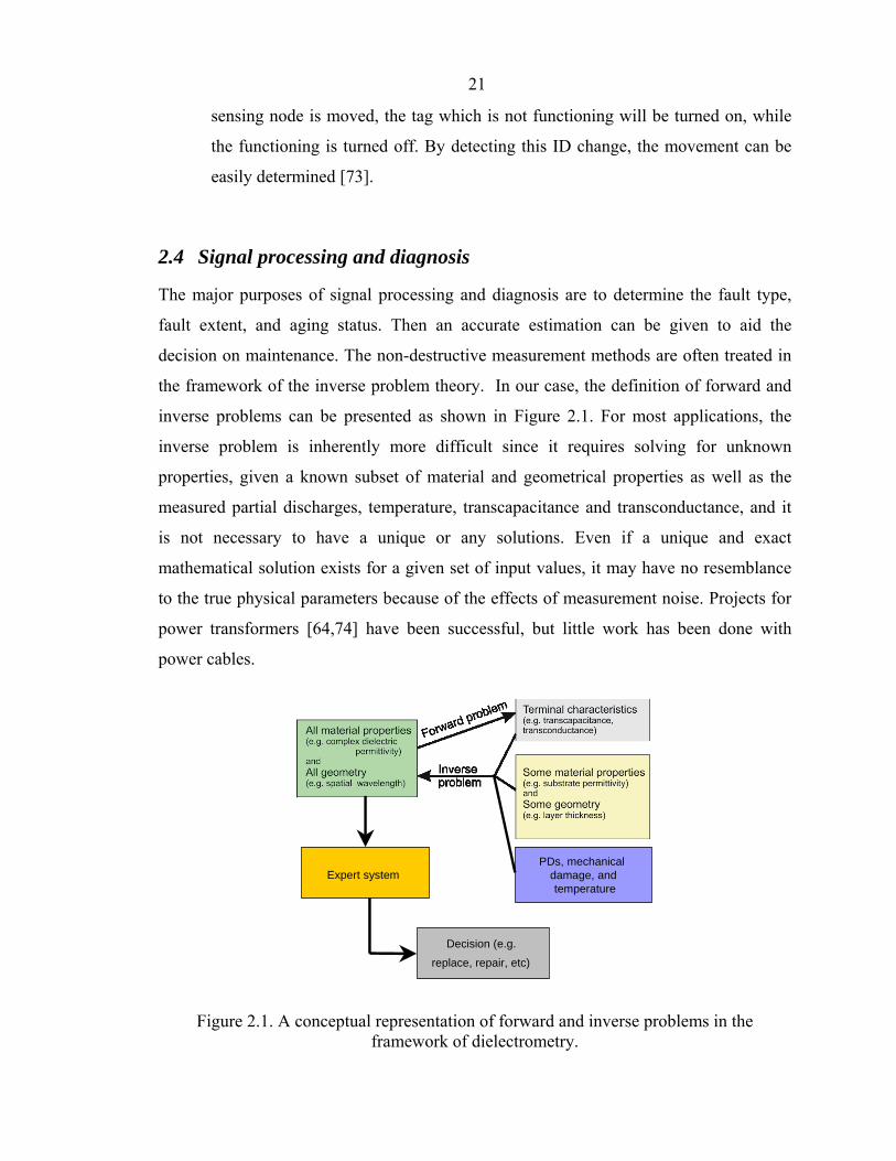
2.4 Signal processing and diagnosis
The major purposes of signal processing and diagnosis are to determine the fault type,
fault extent, and aging status. Then an accurate estimation can be given to aid the
decision on maintenance. The non-destructive measurement methods are often treated in
the framework of the inverse problem theory. In our case, the definition of forward and
inverse problems can be presented as shown in Figure 2.1. For most applications, the
inverse problem is inherently more difficult since it requires solving for unknown
properties, given a known subset of material and geometrical properties as well as the
measured partial discharges, temperature, transcapacitance and transconductance, and it
is not necessary to have a unique or any solutions. Even if a unique and exact
mathematical solution exists for a given set of input values, it may have no resemblance
to the true physical parameters because of the effects of measurement noise. Projects for
power transformers [64,74] have been successful, but little work has been done with
power cables.
Expert system
Decision (e.g.
replace, repair, etc)
PDs, mechanical damage, andtemperature
Figure 2.1. A conceptual representation of forward and inverse problems in the framework of dielectrometry.
22
Several experiments have determined the detection limits for acoustic PD signals in a
cable joint made from EPDM rubber. Results showed that there were several propagation
modes: high frequency is dominant when the sensor is close to the PD source, whereas
low frequency is dominant when the sensor is away from the PD source [75]. Acoustic
emission spectral analysis has identified the types of PDs: point-plane type discharge in
oil, surface discharges in oil, gas bubble discharge in oil, and discharges in indeterminate-
potential particles moving in oil [76]. Thus, a specific type of PD can be identified if
suitable spectral descriptors are selected. However, the result was limited to pattern
identification of partial discharges in oil. A back-propagation (BP) artificial neural
network (ANN) using acoustic emission measurement on PDs with high voltage cables
was investigated. The signals were processed with three-dimensional patterns and short
duration Fourier Transforms (SDFT) [77].
Regular shape and arrangement of voids can also be identified using this method.
However, voids observed in practical conditions are generally irregular, and no method
yet exists to identify the irregular voids that are common in power systems. MLP Neural
Network [78,79], fuzzy logic [80], fracture geometry feature [81], statistic estimation
[82], and wavelet techniques [83] have also been used to analyze PDs. Current practice
still relies heavily on human expertise in the identification and location of PD sources in
electrical apparatus and cables [79]. Future research might focus on developing more
powerful noise rejection procedures; improving the reliability of monitoring systems; and
designing sophisticated expert-systems which can integrate multiple data for quick
recognition of dangerous PD faults [84].
Several sensors used together for insulation estimation can supplement each other to
supply more information. However, still no available signal-processing methods can
perform temperature, mechanical, PD, and dielectrometry measurements for a multi-
sensor system. An important task is to develop an algorithm that can integrate multiple
signals and access accurately the status of insulation.

23
2.5 Scientific challenges
This dissertation identifies some of the scientific challenges to be conquered before the
desired system becomes fully effective. Such problems include the following:
• When the cable system is confined to a tight space, the mobile robot must be small
enough to patrol the space and negotiate all obstacles along its path.
Power cables are usually laid out in a limited space, such as in tunnels, pipes, or
troughs. Frequently, the surfaces of the guide and the cable are not smooth. The cables
are fixed in the guide with fixtures, and branches are along the network. The robot
requires extra abilities to negotiate obstacles and maintain its stability. This must be
accomplished in both autonomous and remote control modes.
• Sensor selection is a challenge. Only non-destructive, miniature, and low-power
sensing technologies are suitable, and they must be effective in detecting the types of
incipient faults.
The sensor and the sensor system must have a small size, high resolution, low-power
consumption, and low cost. One type of sensor may be suitable only for measuring
specified characteristics, but a failure could occur for other reasons and exhibit different
phenomena. Therefore a sensor array must be adopted to monitor each aspect of the
system under inspection. Since each sensor element acquires different information, a
complicated signal processing algorithm which can handle all of the data is highly
desirable for correct diagnosis.
Some monitoring sensors cannot function until the robot stops and the sensors are put
into position; other sensors can work continuously. The mobile sensing system requires
additional coordination of the robot and the sensors to prevent unintended damage.
• Passive RFID-enhanced sensor nodes must be able to harvest sufficient power and
consume minimum power. Therefore, the sensor network can be maintenance-free
and suitable for widespread use.
Ideally, a passive RFID-enhanced sensor network could stay in service forever.
However, the following issues must be resolved:
a. The circuit must work well no matter what level of input power. It cannot burn
out due to a high power level, or malfunction due to a low power level.

24
b. The passive sensing node should have a reasonable working range to cover the
assigned area. The power harvesting circuit and the antenna should be able to
catch enough energy, and the digital IC, the RF front-end IC, and integrated
sensor should have low power consumption.
c. The integrated sensor should be CMOS-based, therefore the sensor and the tag IC
can be integrated into a single semiconductor chip.
d. The system should work under existing RFID communication protocols.
• Autonomous operation in an unstructured environment
The ultimate test of a robot’s effectiveness is its operation in an unstructured
environment. Unlike a laboratory environment, the robot must work in the autonomous
mode. The ubiquitous monitoring system should demonstrate reasonable results.

25
Chapter 3. Economical Analysis
3.1 Introduction
In today’s deregulated environment, utility companies still believe that the ideal power
network is one that operates continuously and without failures. This ideal can be
approached with preventive maintenance and prudent investment -- preferably without
sacrificing reliability. However, preventive maintenance does not always result in cost
efficiency. For instance, it is absurd to assume a “zero tolerance” approach since a utility
would accrue additional financial losses from replacing every cable with a minor failure
that is typical in normal system operations. Therefore, utilities attempt to develop an
optimum cost-efficient maintenance strategy at a minimum operational cost [4].
3.2 Economical rule
Since a minimum operational cost is a necessary condition for maximizing profit, a
simplified economic model includes the controllable operational cost, but not the
fluctuating price of energy. To achieve minimum operational cost when applying
maintenance strategies to a power system, the following rule is applied:
( ) ( )min min F F M MC C Cλ λ= + (3.1)
where C is the total operational cost, FC is the loss due to failures, MC is the
maintenance cost, and Fλ and Mλ are the weighting factors for FC and MC ,
respectively. The weighting factors accommodate a utility’s concerns regarding failures

26
and maintenance. A utility emphasizing service and long-term benefits would use a larger
value for Fλ than the value of Mλ . For the purpose of this paper, Fλ and Mλ assume an
identical value of 1. Further, FC and MC can be explicated as equation (3.2) to (3.5)
/F B C PC C C= + (3.2)
B unit cusC P P T= (3.3)
/C P unit penC C T C= + (3.4)
M MON RC C C= + (3.5)
where BC is the loss due to undelivered power, unitP is the unit price of energy, cusP is
unclaimed (due to the failure) power consumption, T is the failure period, /C PC is the
compensation cost, unitC is the unit compensation, penC is the penalty which utilities may
be required to pay customers in the event of serious failures, MONC is the cost of
monitoring, and RC is the cost of repair/replacement of the power network/components.
Generally, BC can be ignored because of its minor value (i.e., the price of energy will not
affect the applications of maintenance strategies).
In analyzing the dependent relationship of maintenance and failure trends, the
following facts become evident:
When no maintenance is performed on a specified system, failure is unavoidable,
and FC reaches its maximum value.
Increasing MC can lower FC , and the relationship between MC and FC is
generally nonlinear.
After a certain value, increasing MC has a very small effect on FC .
Based on these observations, Figure 3.1 shows a simplified function model
( )F MC f C= . The three zones in the model represent the different effects of MC on FC :
FC decreases while MC increases within zone A. The influence of MC on FC is
increasing.
When MC reaches a critical point, a small increase in MC results in a large
decrease of FC within zone B.
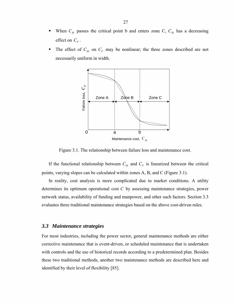
27
When MC passes the critical point b and enters zone C, MC has a decreasing
effect on FC .
The effect of MC on FC may be nonlinear; the three zones described are not
necessarily uniform in width.
MC
FC
FC
Maintenance cost,
0
Failu
re lo
ss,
ba
Zone A Zone B Zone C
Figure 3.1. The relationship between failure loss and maintenance cost.
If the functional relationship between MC and FC is linearized between the critical
points, varying slopes can be calculated within zones A, B, and C (Figure 3.1).
In reality, cost analysis is more complicated due to market conditions. A utility
determines its optimum operational cost C by assessing maintenance strategies, power
network status, availability of funding and manpower, and other such factors. Section 3.3
evaluates three traditional maintenance strategies based on the above cost-driven rules.
3.3 Maintenance strategies
For most industries, including the power sector, general maintenance methods are either
corrective maintenance that is event-driven, or scheduled maintenance that is undertaken
with controls and the use of historical records according to a predetermined plan. Besides
these two traditional methods, another two maintenance methods are described here and
identified by their level of flexibility [85].

28
3.3.1 Corrective/emergency maintenance (CM)
Corrective maintenance (CM) is passive: i.e., there is no action until a failure occurs. CM
is economically efficient when failures cause only minimum inconvenience and financial
loss for the customers. For many years, CM was the favored maintenance strategy for
power cables. Equations (3.1) through (3.5) show no monitoring costs from
implementing this strategy (other costs are still present, however). Let us assume that a
minimum operational cost MINC exists when an optimal maintenance strategy is applied.
Thus, (3.1) can be rewritten for CM as
MIN F RC C C≤ + (3.6)
which demonstrates that CM could be practical if and only if the right side of equation
(3.6) is close to MINC . Examples of power networks for which CM is a reasonable choice
include a new, perfectly installed non-critical distribution network and an underwater
cable network. Using current technology, the cost of prophylactic maintenance is too low
in the first example and too high in the second. If unnecessary monitoring is imposed in
these situations, the total operational cost C may have the characteristics shown in
Figure 3.2.
MC
FC
FC
Maintenance cost,
0
Failu
re lo
ss,
ba
Zone A Zone B Zone C
Figure 3.2. The relationship between failure loss and maintenance cost.
Generally, CM is unacceptable when the right side of (3.6) increases to a critical
level. For example, an unexpected power shutdown to some customers could be too

29
expensive for the utility and the customers because of high compensation and emergency
maintenance costs.
3.3.2 Scheduled maintenance (SM)
As the name suggests, scheduled maintenance (SM) is planned and carried out in
predetermined time intervals to prevent possible failures. SM includes routine monitoring
and network repair, or part replacement when incipient faults are detected by routine
monitoring or predicted by estimation.
It is inherently difficult to determine optimum maintenance time intervals. Since the
standard used to estimate network/components lifetime is generally conservative, losses
are generated if network/components are replaced prematurely, meaning that RC
increases in (3.5). On the other hand, failure risk increases as components approach their
predicted life expectancy.
3.3.3 Condition-based maintenance (CBM)
Condition-based maintenance (CBM) is defined as planned maintenance based on
periodic or continuous monitoring of equipment status. CBM is very attractive since
action is taken only when required. By predicting failure, CBM helps to extend the
service lifetime of power systems. CBM has received more attention in recent years as a
viable maintenance method for cable networks. One case study found that network
performance increased 40% and maintenance cost was lowered by a factor of 7 when
cables were repaired but not replaced [4]. Figure 3.3 shows one possible functional
relationship of operational cost when CBM is applied to a power system. The drawbacks
of CBM are its possible unavailability and monitoring cost.
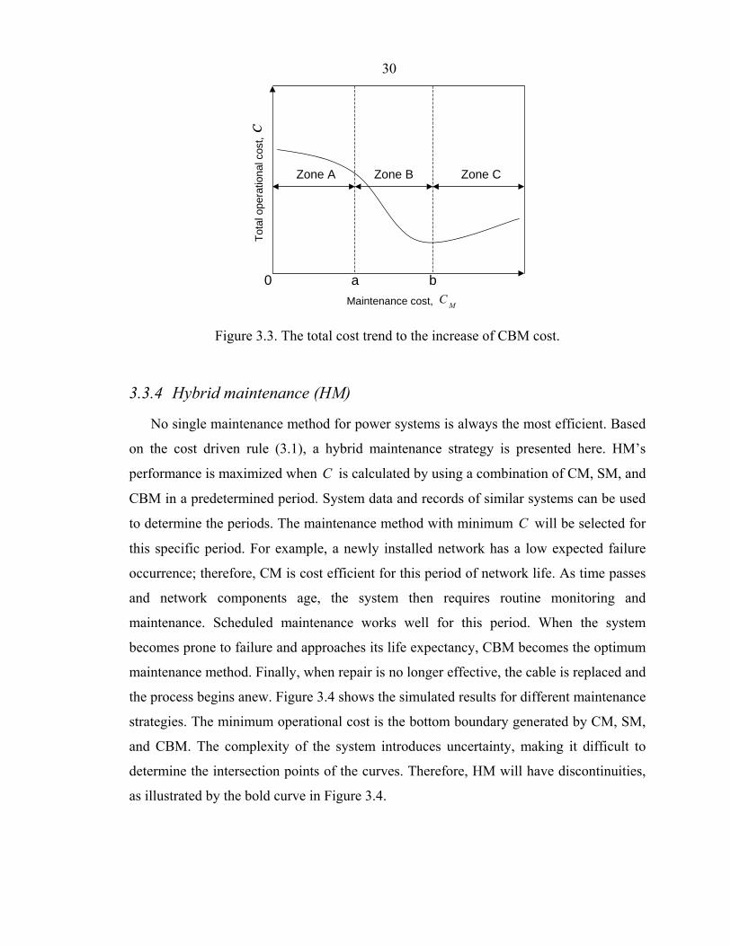
30
MC
CC
Maintenance cost,
0To
tal o
pera
tiona
l cos
t,
ba
Zone A Zone B Zone C
Figure 3.3. The total cost trend to the increase of CBM cost.
3.3.4 Hybrid maintenance (HM)
No single maintenance method for power systems is always the most efficient. Based
on the cost driven rule (3.1), a hybrid maintenance strategy is presented here. HM’s
performance is maximized when C is calculated by using a combination of CM, SM, and
CBM in a predetermined period. System data and records of similar systems can be used
to determine the periods. The maintenance method with minimum C will be selected for
this specific period. For example, a newly installed network has a low expected failure
occurrence; therefore, CM is cost efficient for this period of network life. As time passes
and network components age, the system then requires routine monitoring and
maintenance. Scheduled maintenance works well for this period. When the system
becomes prone to failure and approaches its life expectancy, CBM becomes the optimum
maintenance method. Finally, when repair is no longer effective, the cable is replaced and
the process begins anew. Figure 3.4 shows the simulated results for different maintenance
strategies. The minimum operational cost is the bottom boundary generated by CM, SM,
and CBM. The complexity of the system introduces uncertainty, making it difficult to
determine the intersection points of the curves. Therefore, HM will have discontinuities,
as illustrated by the bold curve in Figure 3.4.
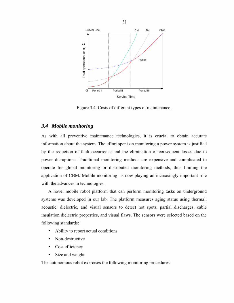
31
CC
Service Time
0
Tota
l ope
ratio
nal c
ost,
Period I Period II Period III
CM SM CBMCritical Line
Hybrid
Figure 3.4. Costs of different types of maintenance.
3.4 Mobile monitoring
As with all preventive maintenance technologies, it is crucial to obtain accurate
information about the system. The effort spent on monitoring a power system is justified
by the reduction of fault occurrence and the elimination of consequent losses due to
power disruptions. Traditional monitoring methods are expensive and complicated to
operate for global monitoring or distributed monitoring methods, thus limiting the
application of CBM. Mobile monitoring is now playing an increasingly important role
with the advances in technologies.
A novel mobile robot platform that can perform monitoring tasks on underground
systems was developed in our lab. The platform measures aging status using thermal,
acoustic, dielectric, and visual sensors to detect hot spots, partial discharges, cable
insulation dielectric properties, and visual flaws. The sensors were selected based on the
following standards:
Ability to report actual conditions
Non-destructive
Cost efficiency
Size and weight
The autonomous robot exercises the following monitoring procedures:
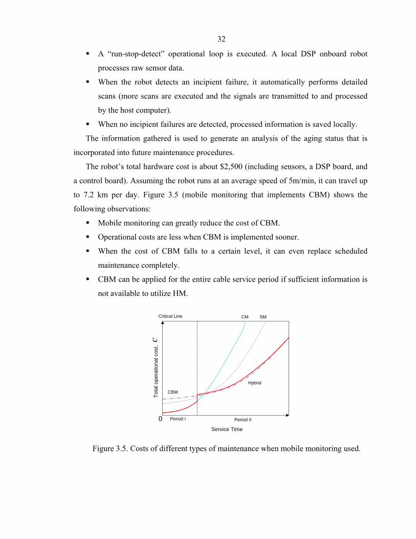
32
A “run-stop-detect” operational loop is executed. A local DSP onboard robot
processes raw sensor data.
When the robot detects an incipient failure, it automatically performs detailed
scans (more scans are executed and the signals are transmitted to and processed
by the host computer).
When no incipient failures are detected, processed information is saved locally.
The information gathered is used to generate an analysis of the aging status that is
incorporated into future maintenance procedures.
The robot’s total hardware cost is about $2,500 (including sensors, a DSP board, and
a control board). Assuming the robot runs at an average speed of 5m/min, it can travel up
to 7.2 km per day. Figure 3.5 (mobile monitoring that implements CBM) shows the
following observations:
Mobile monitoring can greatly reduce the cost of CBM.
Operational costs are less when CBM is implemented sooner.
When the cost of CBM falls to a certain level, it can even replace scheduled
maintenance completely.
CBM can be applied for the entire cable service period if sufficient information is
not available to utilize HM.
CC
Service Time
0
Tota
l ope
ratio
nal c
ost,
Period I Period II
CM SM
CBM
Critical Line
Hybrid
Figure 3.5. Costs of different types of maintenance when mobile monitoring used.

33
3.5 Conclusions
Based on the derived cost-driven model, an economic assessment can be performed for
traditional corrective maintenance, scheduled maintenance, and condition-based
maintenance. The hybrid maintenance method derived can nearly reach the minimum
operational cost by combining the advantages of the other strategies. Mobile monitoring
incorporating CBM produces the lowest cost. Therefore, it is a viable maintenance
strategy.

34
Chapter 4. Mobile Robot Platform
4.1 Introduction
Designing a mobile robot for underground systems is more complex than designing
pipe- and power-line-crawling robots. Figure 4.1 shows a typical example of the cables
and their surroundings in a 14 kV underground installation at the University of
Washington. Cables lie in metal troughs that are generally 25 to 18 cm wide and 5 cm
deep. Because the cables can “lay” anywhere within the troughs, and the troughs
themselves are often stacked on top of one another, the available space is usually about
11 cm. Although longitudinal space is somewhat flexible, overall height is a limiting
factor. There are no sharp turns since the minimum radius of curvature for a cable is on
the order of meters. The traveling robot may encounter minor obstructions such as splices
and mounting brackets that it must negotiate without toppling over. This chapter
describes the design of the robotic platform, including the mechanical design, control
circuit board design, and control panel design. Some of challenges are described below.

35
Figure 4.1. Two underground cables in metal troughs.
4.1.1 Motion patterns of robot platforms
Inspection robots are either external or internal. External robots travel over the outer
surfaces of cables and conductors and may possess a high degree of autonomy. Internal
robots travel inside ducts and pipes and often follow a predetermined route (if they are
equipped with track-finding devices) and conduct a limited set of operations (Figure 4.2).
Complexity and the level of autonomy determine the selection of the appropriate motion
pattern. External travel is generally preferred because an internal robot usually requires
an additional guide inside the cable (which can impair the integrity of the cable), and
spatial limitations may limit its sensing functions.

36
(a) Internal platform
Modular mobile sensor platform
Power andcommunicationsmodule
Fringing electric fieldsensor array
Acoustic andinfrared sensors
Motion actuatorsCable
Pipe
(b) External platform
Figure 4.2. Conceptual design of robotic platforms.
4.1.2 Power supply
It is awkward for the inspecting robot to drag a power cord behind it in the cable
network’s distributed system. Ideally, the power supply should be wireless. It is desirable
that the platform harvests energy from energized cables (preferably, inductive coupling
for a wireless power supply). Although the low frequency coupling is less efficient than
microwave mode [14], direct proximity to the power cable makes it a more viable choice.
The platform requires an independent backup power source as well.

37
4.1.3 Control strategy
Control strategy includes object tracking, collision avoidance, and prevention of
electrical short circuits. The control system receives initial commands from the operator
for the global tasks, and small tasks are often pre-programmed. The most important
requirements are:
a) The control should be robust because of the complicated motions required and the
irregular surface of the cable connections.
b) There should be an optimum algorithm to locate the sensor array with respect to
the inspected system; a path planning algorithm to track the entire or part of the
network with the shortest path; and control sequences to adaptively switch sensor
operations from fast (superficial inspection) to slow (detailed inspection) modes.
c) The control algorithm must also manage mobile monitoring team operations
(robots must cooperate and share data).
4.1.4 Communication
The communication module exchanges data between the master (host) computer and
the mobile robot, including data originating from different streams on both sides of the
communication link and their different priorities. Wireless communication is
implemented through transition stations distributed along the cable network. A
multiplexing problem concerning the allocation between local and remote computation
capacity must be resolved.
4.1.5 Signal processing strategies
The robot requires considerable computational resources to be adaptive and flexible.
The size limitations mandated by underground applications strongly favor wireless
communication and off-board intelligence. This also involves allocation between local
and remote signal processing.
4.1.6 Positioning system
The positioning system should function much like a Global Positioning System
(GPS). Once the system is implemented, effective maintenance and rescue tasks for cable

38
systems, and even for the robot itself, can be carried out. Most applications employ
relative and absolute positioning. Relative positioning can provide a rough estimate of
location, and absolute positioning can compensate for any errors introduced [16].
4.2 System overview
Figure 4.3 shows a mobile robotic platform developed in our lab. A unique segmented
configuration allows the robot to traverse cables and negotiate obstacles along its path
with a diameter of four to eight centimeters. The platform’s design consists of a multi-
processor control board, a 900 MHz wireless communication module, a DSP board, and
multiple sensors. Figure 4.4 shows the information flow of the system.
Figure 4.3. Robot platform.
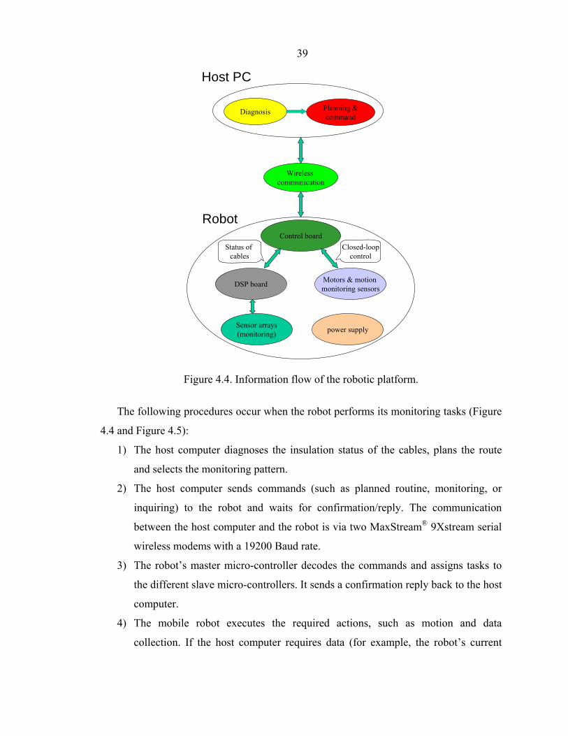
39
Host PC
Diagnosis Planning &command
Wireless communication
Motors & motion monitoring sensors
Sensor arrays(monitoring)
Control board
power supply
Closed-loopcontrol
Status of cables
Robot
DSP board
Figure 4.4. Information flow of the robotic platform.
The following procedures occur when the robot performs its monitoring tasks (Figure
4.4 and Figure 4.5):
1) The host computer diagnoses the insulation status of the cables, plans the route
and selects the monitoring pattern.
2) The host computer sends commands (such as planned routine, monitoring, or
inquiring) to the robot and waits for confirmation/reply. The communication
between the host computer and the robot is via two MaxStream® 9Xstream serial
wireless modems with a 19200 Baud rate.
3) The robot’s master micro-controller decodes the commands and assigns tasks to
the different slave micro-controllers. It sends a confirmation reply back to the host
computer.
4) The mobile robot executes the required actions, such as motion and data
collection. If the host computer requires data (for example, the robot’s current
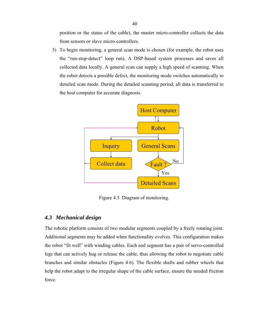
40
position or the status of the cable), the master micro-controller collects the data
from sensors or slave micro-controllers.
5) To begin monitoring, a general scan mode is chosen (for example, the robot uses
the “run-stop-detect” loop run). A DSP-based system processes and saves all
collected data locally. A general scan can supply a high speed of scanning. When
the robot detects a possible defect, the monitoring mode switches automatically to
detailed scan mode. During the detailed scanning period, all data is transferred to
the host computer for accurate diagnosis.
Host Computer
Robot
General Scans
Fault ?
Detailed Scans
No
Yes
Inquiry
Collect data
Figure 4.5. Diagram of monitoring.
4.3 Mechanical design
The robotic platform consists of two modular segments coupled by a freely rotating joint.
Additional segments may be added when functionality evolves. This configuration makes
the robot “fit well” with winding cables. Each end segment has a pair of servo-controlled
legs that can actively hug or release the cable, thus allowing the robot to negotiate cable
branches and similar obstacles (Figure 4.6). The flexible shafts and rubber wheels that
help the robot adapt to the irregular shape of the cable surface, ensure the needed friction
force.

41
Figure 4.6. Mechanical design of the robotic platform.
An unsolved problem still exists with this design: it is very difficult for the robot to
stay on the top of the cable, since the robot’s circular movement is not controllable.
Therefore, a new platform with the addition of a steering system added has been
successfully developed (Figure 4.7). We believe that adding an accelerometer sensor
ADXL202 will help determine the robot’s position in a vertical direction, (i.e. the circular
slippage). Adjusting the angle of the steering wheel will bring the robot back to the top of
the cable. Other enhancements include the adoption of DC motors for the main drive and
an encoder for speed measurement. The speed of the robot can be improved greatly with
DC motors. While many of the sensors do not require contact with the cable, some, such
as the acoustic emission sensor, must have proper contact with the cable surface in order
to take accurate measurements. A servo-powered linear actuator is used to periodically
lower sensing equipment to monitor the power distribution line. Figure 4.7 shows the
robot on a cable and trough installation in an underground service tunnel. In the
foreground is the front drive section, followed by a set of stabilizers and a section for
carrying sensors.
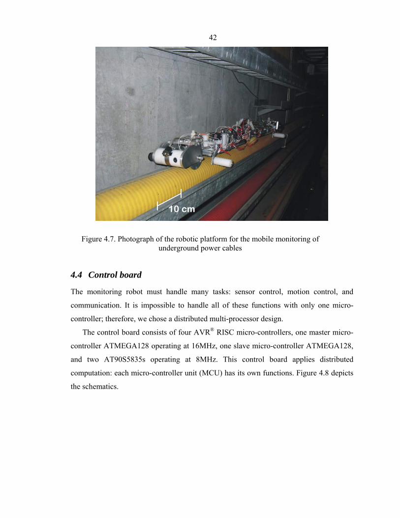
42
10 cm
Figure 4.7. Photograph of the robotic platform for the mobile monitoring of
underground power cables
4.4 Control board
The monitoring robot must handle many tasks: sensor control, motion control, and
communication. It is impossible to handle all of these functions with only one micro-
controller; therefore, we chose a distributed multi-processor design.
The control board consists of four AVR® RISC micro-controllers, one master micro-
controller ATMEGA128 operating at 16MHz, one slave micro-controller ATMEGA128,
and two AT90S5835s operating at 8MHz. This control board applies distributed
computation: each micro-controller unit (MCU) has its own functions. Figure 4.8 depicts
the schematics.
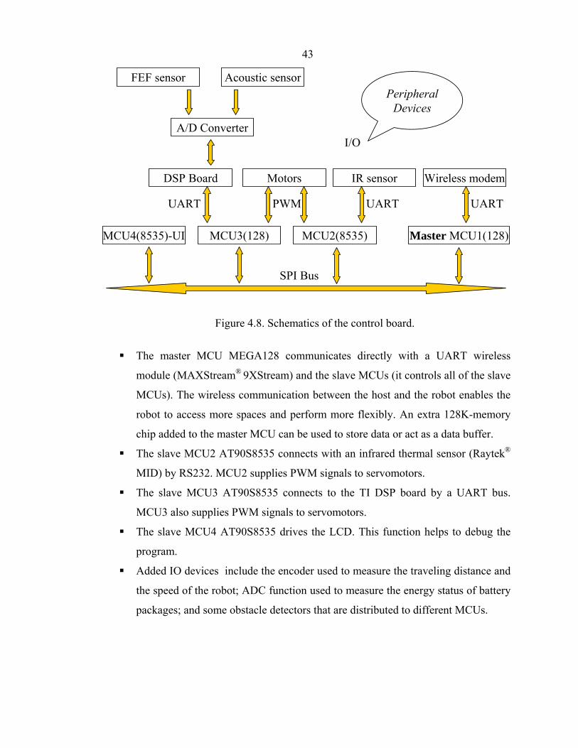
43
Wireless modem
Master MCU1(128)
Motors
UART
IR sensor
MCU3(128)
FEF sensor
MCU2(8535)
UART
MCU4(8535)-UI
SPI Bus
UART
DSP Board
A/D Converter
Acoustic sensorPeripheral
Devices
PWM
I/O
Figure 4.8. Schematics of the control board.
The master MCU MEGA128 communicates directly with a UART wireless
module (MAXStream® 9XStream) and the slave MCUs (it controls all of the slave
MCUs). The wireless communication between the host and the robot enables the
robot to access more spaces and perform more flexibly. An extra 128K-memory
chip added to the master MCU can be used to store data or act as a data buffer.
The slave MCU2 AT90S8535 connects with an infrared thermal sensor (Raytek®
MID) by RS232. MCU2 supplies PWM signals to servomotors.
The slave MCU3 AT90S8535 connects to the TI DSP board by a UART bus.
MCU3 also supplies PWM signals to servomotors.
The slave MCU4 AT90S8535 drives the LCD. This function helps to debug the
program.
Added IO devices include the encoder used to measure the traveling distance and
the speed of the robot; ADC function used to measure the energy status of battery
packages; and some obstacle detectors that are distributed to different MCUs.
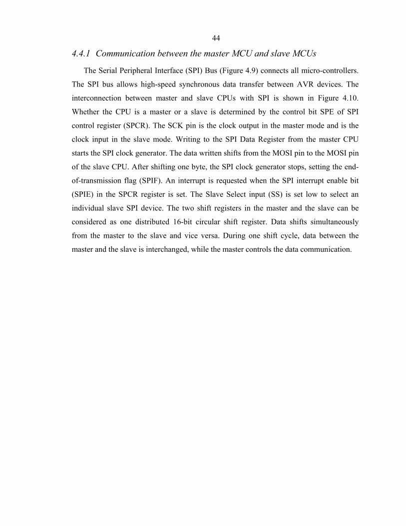
44
4.4.1 Communication between the master MCU and slave MCUs
The Serial Peripheral Interface (SPI) Bus (Figure 4.9) connects all micro-controllers.
The SPI bus allows high-speed synchronous data transfer between AVR devices. The
interconnection between master and slave CPUs with SPI is shown in Figure 4.10.
Whether the CPU is a master or a slave is determined by the control bit SPE of SPI
control register (SPCR). The SCK pin is the clock output in the master mode and is the
clock input in the slave mode. Writing to the SPI Data Register from the master CPU
starts the SPI clock generator. The data written shifts from the MOSI pin to the MOSI pin
of the slave CPU. After shifting one byte, the SPI clock generator stops, setting the end-
of-transmission flag (SPIF). An interrupt is requested when the SPI interrupt enable bit
(SPIE) in the SPCR register is set. The Slave Select input (SS) is set low to select an
individual slave SPI device. The two shift registers in the master and the slave can be
considered as one distributed 16-bit circular shift register. Data shifts simultaneously
from the master to the slave and vice versa. During one shift cycle, data between the
master and the slave is interchanged, while the master controls the data communication.
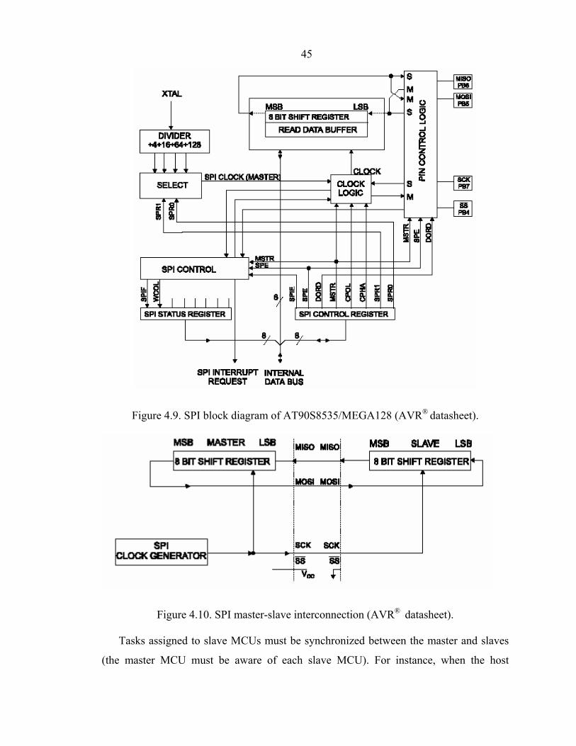
45
Figure 4.9. SPI block diagram of AT90S8535/MEGA128 (AVR® datasheet).
Figure 4.10. SPI master-slave interconnection (AVR® datasheet).
Tasks assigned to slave MCUs must be synchronized between the master and slaves
(the master MCU must be aware of each slave MCU). For instance, when the host
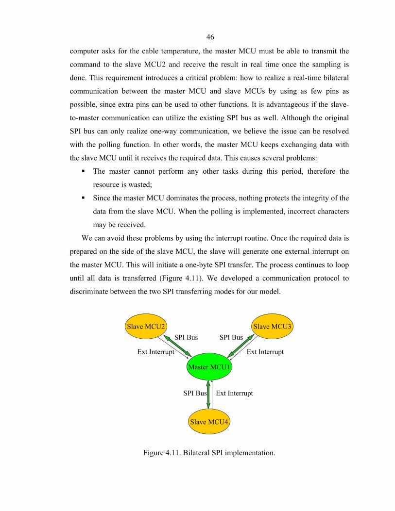
46
computer asks for the cable temperature, the master MCU must be able to transmit the
command to the slave MCU2 and receive the result in real time once the sampling is
done. This requirement introduces a critical problem: how to realize a real-time bilateral
communication between the master MCU and slave MCUs by using as few pins as
possible, since extra pins can be used to other functions. It is advantageous if the slave-
to-master communication can utilize the existing SPI bus as well. Although the original
SPI bus can only realize one-way communication, we believe the issue can be resolved
with the polling function. In other words, the master MCU keeps exchanging data with
the slave MCU until it receives the required data. This causes several problems:
The master cannot perform any other tasks during this period, therefore the
resource is wasted;
Since the master MCU dominates the process, nothing protects the integrity of the
data from the slave MCU. When the polling is implemented, incorrect characters
may be received.
We can avoid these problems by using the interrupt routine. Once the required data is
prepared on the side of the slave MCU, the slave will generate one external interrupt on
the master MCU. This will initiate a one-byte SPI transfer. The process continues to loop
until all data is transferred (Figure 4.11). We developed a communication protocol to
discriminate between the two SPI transferring modes for our model.
Slave MCU4
Slave MCU3Slave MCU2SPI Bus
SPI Bus
SPI Bus
Ext Interrupt Ext Interrupt
Ext Interrupt
Master MCU1
Figure 4.11. Bilateral SPI implementation.
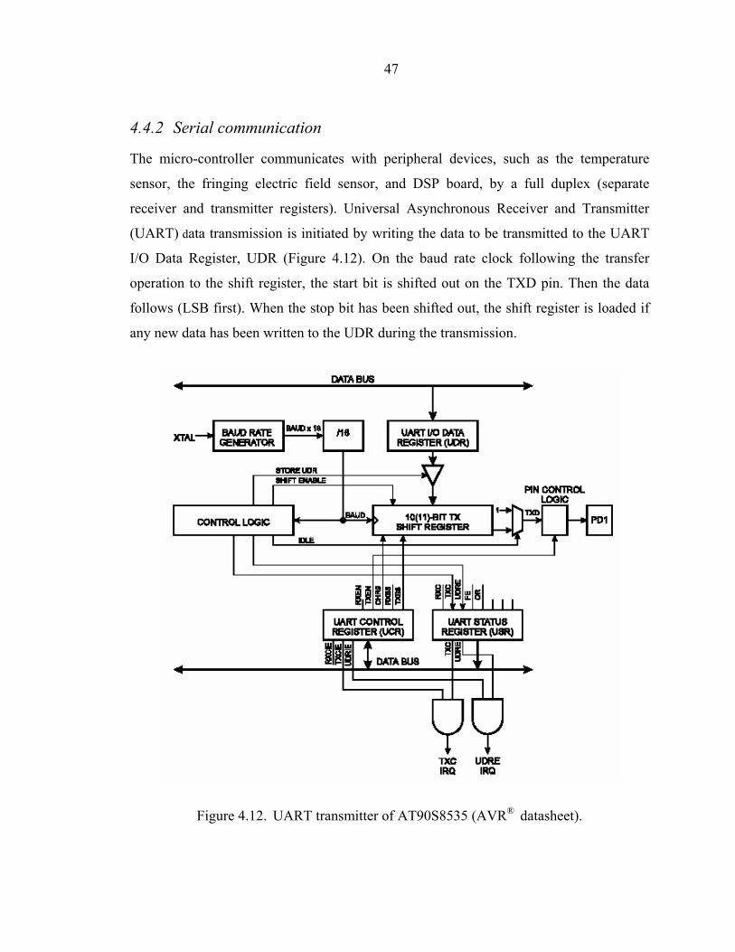
47
4.4.2 Serial communication
The micro-controller communicates with peripheral devices, such as the temperature
sensor, the fringing electric field sensor, and DSP board, by a full duplex (separate
receiver and transmitter registers). Universal Asynchronous Receiver and Transmitter
(UART) data transmission is initiated by writing the data to be transmitted to the UART
I/O Data Register, UDR (Figure 4.12). On the baud rate clock following the transfer
operation to the shift register, the start bit is shifted out on the TXD pin. Then the data
follows (LSB first). When the stop bit has been shifted out, the shift register is loaded if
any new data has been written to the UDR during the transmission.
Figure 4.12. UART transmitter of AT90S8535 (AVR® datasheet).
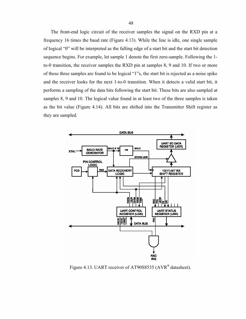
48
The front-end logic circuit of the receiver samples the signal on the RXD pin at a
frequency 16 times the baud rate (Figure 4.13). While the line is idle, one single sample
of logical “0” will be interpreted as the falling edge of a start bit and the start bit detection
sequence begins. For example, let sample 1 denote the first zero-sample. Following the 1-
to-0 transition, the receiver samples the RXD pin at samples 8, 9 and 10. If two or more
of these three samples are found to be logical “1”s, the start bit is rejected as a noise spike
and the receiver looks for the next 1-to-0 transition. When it detects a valid start bit, it
performs a sampling of the data bits following the start bit. These bits are also sampled at
samples 8, 9 and 10. The logical value found in at least two of the three samples is taken
as the bit value (Figure 4.14). All bits are shifted into the Transmitter Shift register as
they are sampled.
Figure 4.13. UART receiver of AT90S8535 (AVR® datasheet).

49
Figure 4.14. Sampling received data (AVR® datasheet).
4.5 Internet remote control
A complementary PC application was developed in parallel with the platform to control
the robot and analyze gathered data. The software was designed with a modular
architecture to facilitate the addition of functional modules rather than integrating new
code into a monolithic program. The resulting architecture consists of a suite of modules
that interact through software sockets as shown in Figure 4.15.
Main Control
Data Visualization
Data ProcessingCommunication
Socket
SocketSocke
t
Main Control
Data Visualization
Data ProcessingCommunication
Socket
SocketSocke
t
Figure 4.15. Modular software architecture for robot control.
Each module communicates with the main control program via bi-directional
asynchronous software socket connections. The main control program issues high-level
commands and routes data between the functional modules. For instance, the main
control module can issue high-level commands to the communication module, which in
turn relays the signal to the robot. The data processing and data visualization modules
have not yet been implemented.
The current system allows a technician to control a remote distributed network of
power line inspection robots via a LAN or dial-up connection. Figure 4.16 shows a
distributed client/server model.
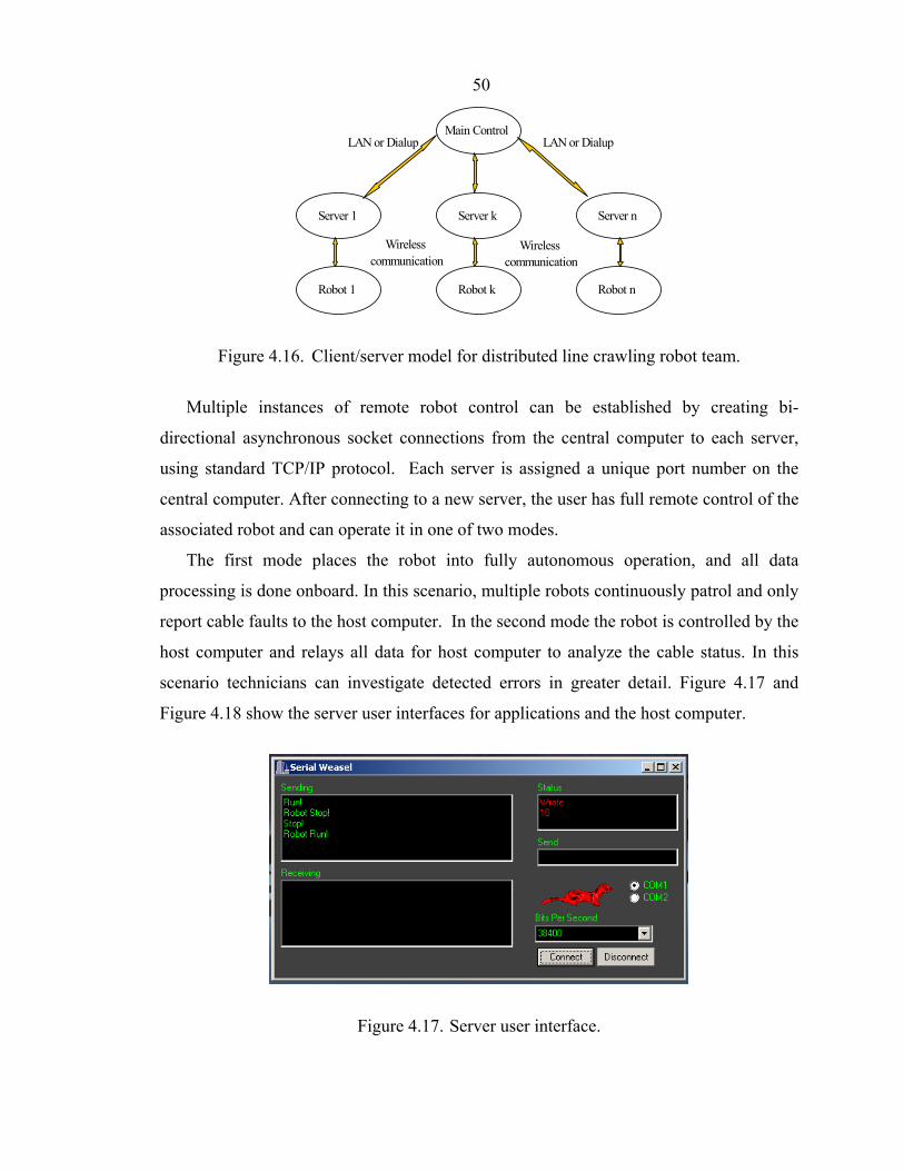
50
Main Control
Server n Server 1
LAN or DialupLAN or Dialup
Robot 1 Robot n
Server k
Robot k
Wireless communication
Wireless communication
Figure 4.16. Client/server model for distributed line crawling robot team.
Multiple instances of remote robot control can be established by creating bi-
directional asynchronous socket connections from the central computer to each server,
using standard TCP/IP protocol. Each server is assigned a unique port number on the
central computer. After connecting to a new server, the user has full remote control of the
associated robot and can operate it in one of two modes.
The first mode places the robot into fully autonomous operation, and all data
processing is done onboard. In this scenario, multiple robots continuously patrol and only
report cable faults to the host computer. In the second mode the robot is controlled by the
host computer and relays all data for host computer to analyze the cable status. In this
scenario technicians can investigate detected errors in greater detail. Figure 4.17 and
Figure 4.18 show the server user interfaces for applications and the host computer.
Figure 4.17. Server user interface.

51
Figure 4.18. The host computer user interface.
4.6 Conclusions
A mobile robot is developed to work as the mobile platform for underground cable
systems. It is equipped with both a modular design and a legged design. The former can
fit the evolution requirement, while the latter can handle obstacles along the travel path.
The control board is implemented with four distributed micro-controllers, which greatly
increases the robot’s performance. The modified Serial Peripheral Interface Bus and the
corresponding protocol are developed to enhance communications between the master
micro-controller and the slave micro-controllers. Software is developed to aid Internet
control of the robot.

52
Chapter 5. DSP Board Development
5.1 Introduction
When the mobile robot patrols a cable, the human operator can program the sensor
systems for continuous or fixed rate data collection. As mentioned in the previous
chapter, the data is processed locally (on board), or relayed to the host computer for
remote processing (off board). Local signal processing provides a real-time diagnosis but
its computation resources, including hardware, software, and storage space, are limited.
On the other hand, even if the host computer is a super-computer, the slow transfer rate of
wireless communication cannot guarantee the real-time estimation. A digital signal
processor (DSP) based data acquisition/processing system is adopted by using a Texas
Instruments® 150-MHz C6711DSP board capable of executing 900 million floating-point
operations per second (MFLOPS). This DSP-based real-time system processes the
sensing data with acceptable accuracy. The entire data collection system consists of a
C6711DSK, a THS1408EVM ADC board, an over-voltage protector, and sensors (Figure
5.1). Most sensors connect directly to the ADC board, but the control board relays some
data, such as temperature, to the DSP.

53
Cable Sensors
Preamplifier/Amplifier
Over-voltage protector
A/D Converter (THS1408)
DSP Board (C6711)
Data & Address Bus
Control Board
RS232
Figure 5.1. Data acquisition system setup.
5.2 C6711DSK development
The Texas Instruments® C6711DSK offers several outstanding features:
150-MHz C6711DSP capable of executing 900 million floating-point
operations per second (MFLOPS)
Dual clock support, CPU at 150MHz and external memory interface (EMIF)
at 100MHz
16M Bytes of 100 MHz synchronous dynamic random access memory
(SDRAM)
128K Bytes of flash programmable and erasable read only memory (ROM),
where the program for the stand-alone DSP is written
8-bit memory-mapped I/O port
Expansion memory and peripheral connectors for daughter board support

54
5.2.1 Data transferring between ADC and DSP
In a real-time system, it is important to interpret and control data flow to achieve high
performance. In general, the CPU should be used only for sporadic (non-periodic) access
to individual devices or memory locations; otherwise, the system could sustain
performance degradation. We found it best to use the available direct memory access
(DMA) controller for background off-chip data accesses, and schedule the CPU for other
tasks during the same time. When the data transfer is finished, the DMA will trigger an
interrupt to the CPU, which will then process any “leftover” tasks. The flexibility of the
CPU and the DMA facilitates code structure and DMA activity that can maximize data
I/O bandwidth for particular situations.
C6711 has an enhanced direct memory access (EDMA) controller (Figure 5.2) which
can handle data transfers between the level-two (L2) cache/memory controller and the
device peripherals. The transfers include cache servicing, non-cacheable memory
accesses, user-programmed data transfers, and host accesses. However, EDMA accesses
are allowed only to L2 space that is configured as mapped SRAM. In the TMS320C6711,
the L2 is a 64 KB memory that can operate in different modes, all SRAM, 1-Way cache
and ¾ SRAM, 2-Way cache and ½ SRAM, 3-Way cache and ¼ SRAM, or 4-Way cache.
Figure 5.2. TMS320C6711 schematic diagram (Texas Instruments® datasheet).
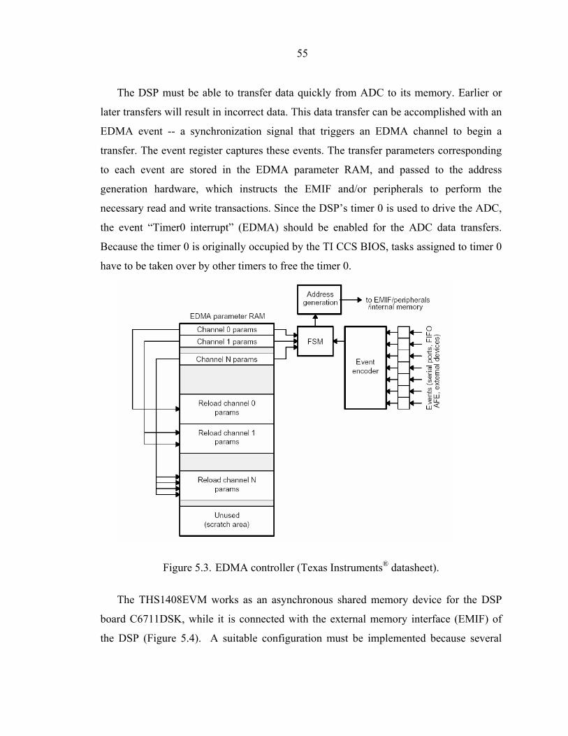
55
The DSP must be able to transfer data quickly from ADC to its memory. Earlier or
later transfers will result in incorrect data. This data transfer can be accomplished with an
EDMA event -- a synchronization signal that triggers an EDMA channel to begin a
transfer. The event register captures these events. The transfer parameters corresponding
to each event are stored in the EDMA parameter RAM, and passed to the address
generation hardware, which instructs the EMIF and/or peripherals to perform the
necessary read and write transactions. Since the DSP’s timer 0 is used to drive the ADC,
the event “Timer0 interrupt” (EDMA) should be enabled for the ADC data transfers.
Because the timer 0 is originally occupied by the TI CCS BIOS, tasks assigned to timer 0
have to be taken over by other timers to free the timer 0.
Figure 5.3. EDMA controller (Texas Instruments® datasheet).
The THS1408EVM works as an asynchronous shared memory device for the DSP
board C6711DSK, while it is connected with the external memory interface (EMIF) of
the DSP (Figure 5.4). A suitable configuration must be implemented because several
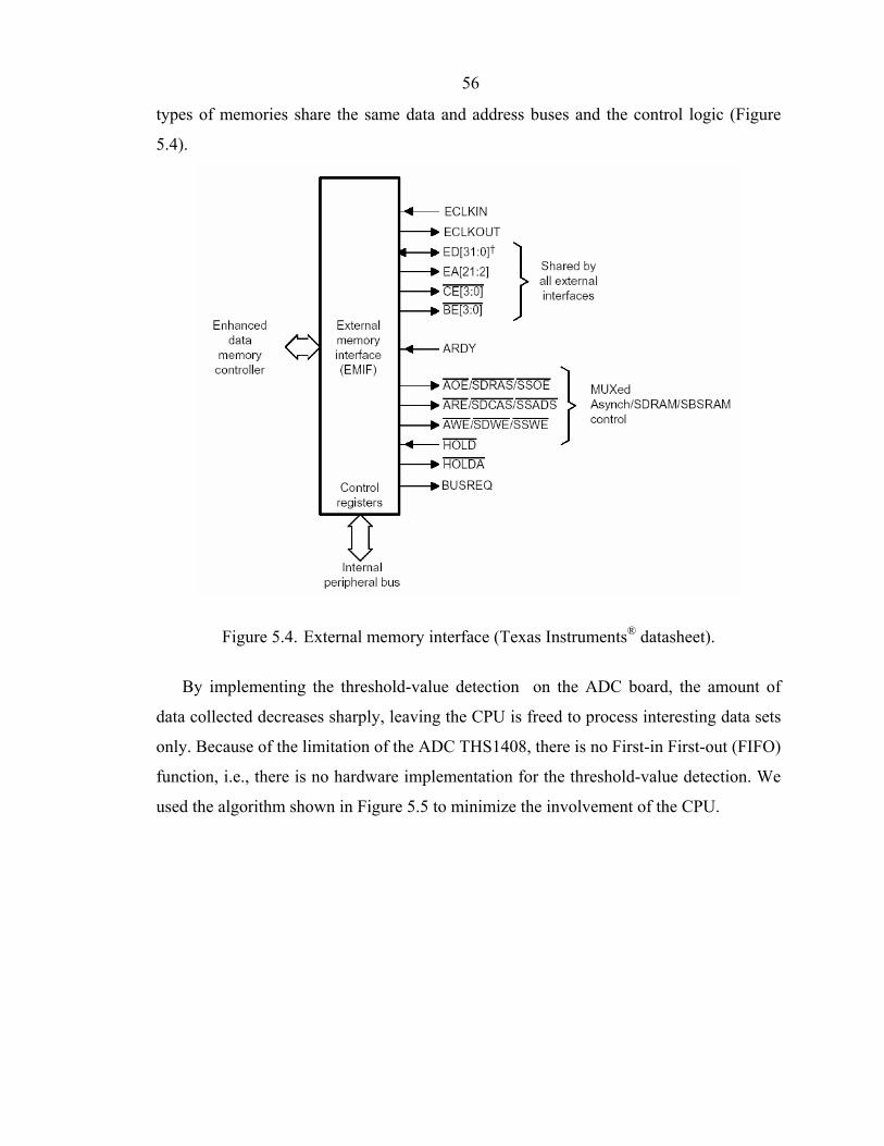
56
types of memories share the same data and address buses and the control logic (Figure
5.4).
Figure 5.4. External memory interface (Texas Instruments® datasheet).
By implementing the threshold-value detection on the ADC board, the amount of
data collected decreases sharply, leaving the CPU is freed to process interesting data sets
only. Because of the limitation of the ADC THS1408, there is no First-in First-out (FIFO)
function, i.e., there is no hardware implementation for the threshold-value detection. We
used the algorithm shown in Figure 5.5 to minimize the involvement of the CPU.

57
Set up the EDMA parameters for one sample
Clear the pending flag,and initiate a new sample
|sample|<Threshold
value
Set up the EDMA parameters for 1K samples
Clear the pending flag,and initiate sampling
Signal processing
Interrupt to the CPU
Interrupt to the CPU
Yes
No
Figure 5.5. Software implementation for threshold detection.
5.2.2 Communication between DSP and the control board
The communication utility between the DSP board and the control board must be able
to perform forward commands from the control board to the DSP board, and transfer the
required data from the DSP board to the control board.
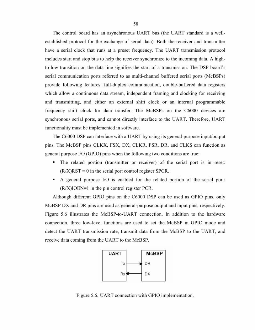
58
The control board has an asynchronous UART bus (the UART standard is a well-
established protocol for the exchange of serial data). Both the receiver and transmitter
have a serial clock that runs at a preset frequency. The UART transmission protocol
includes start and stop bits to help the receiver synchronize to the incoming data. A high-
to-low transition on the data line signifies the start of a transmission. The DSP board’s
serial communication ports referred to as multi-channel buffered serial ports (McBSPs)
provide following features: full-duplex communication, double-buffered data registers
which allow a continuous data stream, independent framing and clocking for receiving
and transmitting, and either an external shift clock or an internal programmable
frequency shift clock for data transfer. The McBSPs on the C6000 devices are
synchronous serial ports, and cannot directly interface to the UART. Therefore, UART
functionality must be implemented in software.
The C6000 DSP can interface with a UART by using its general-purpose input/output
pins. The McBSP pins CLKX, FSX, DX, CLKR, FSR, DR, and CLKS can function as
general purpose I/O (GPIO) pins when the following two conditions are true:
The related portion (transmitter or receiver) of the serial port is in reset:
(R/X)RST = 0 in the serial port control register SPCR.
A general purpose I/O is enabled for the related portion of the serial port:
(R/X)IOEN=1 in the pin control register PCR.
Although different GPIO pins on the C6000 DSP can be used as GPIO pins, only
McBSP DX and DR pins are used as general-purpose output and input pins, respectively.
Figure 5.6 illustrates the McBSP-to-UART connection. In addition to the hardware
connection, three low-level functions are used to set the McBSP in GPIO mode and
detect the UART transmission rate, transmit data from the McBSP to the UART, and
receive data coming from the UART to the McBSP.
Figure 5.6. UART connection with GPIO implementation.

59
5.3 A/D converter board configuration
The analog-to-digital converter THS1408EVM offers the following features:
14-Bit resolution
Up to 8 MSPS speed
Differential nonlinearity (DNL) ±0.6 LSB
Integral nonlinearity (INL) ±1.5 LSB
Internal reference
Differential inputs
Programmable gain amplifier
Timing compatible with TMS320C6000 DSP
The THS1408 core is based on a pipelined architecture with a latency of 9.5 samples,
i.e., the conversion results appear on the digital output 9.5 clock cycles after the input
signal is sampled. The parallel interface of the THS1408 ADC features three-state
buffers, making it possible to connect it directly to the DSP’s parallel data bus. In
addition to the sample results, it is possible to read back the values of the control register,
the PGA gain register, and the offset register. Selecting which register to read is
determined by the address inputs A[1,0], while ADC results are available at address 0.
The board provides an external SMB connection for ADC clock input. This can be
configured as either ac- or dc-coupled. To make the ADC board suitable for different
applications and retain synchronization between the ADC and DSP boards, the DSP’s
timer is used to drive the ADC as the external clock source. The digital lines from the
ADC are buffered before going to the daughter card connectors. The ADC board has
onboard logic that controls the memory mapping of the ADC within the motherboard’s
peripheral memory space, i.e., it does accept all address formats with A[1,0] equal to 0 as
valid ADC addresses (Figure 5.7).
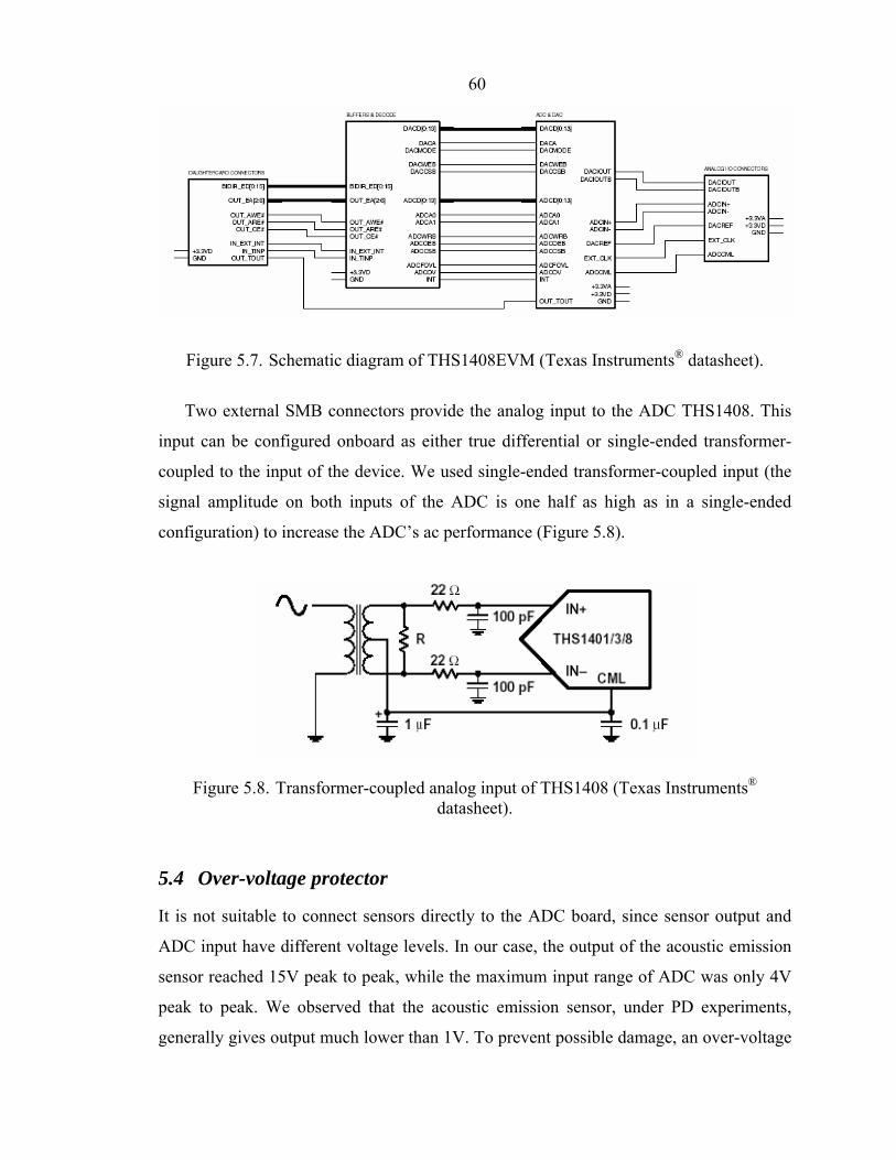
60
Figure 5.7. Schematic diagram of THS1408EVM (Texas Instruments® datasheet).
Two external SMB connectors provide the analog input to the ADC THS1408. This
input can be configured onboard as either true differential or single-ended transformer-
coupled to the input of the device. We used single-ended transformer-coupled input (the
signal amplitude on both inputs of the ADC is one half as high as in a single-ended
configuration) to increase the ADC’s ac performance (Figure 5.8).
Figure 5.8. Transformer-coupled analog input of THS1408 (Texas Instruments® datasheet).
5.4 Over-voltage protector
It is not suitable to connect sensors directly to the ADC board, since sensor output and
ADC input have different voltage levels. In our case, the output of the acoustic emission
sensor reached 15V peak to peak, while the maximum input range of ADC was only 4V
peak to peak. We observed that the acoustic emission sensor, under PD experiments,
generally gives output much lower than 1V. To prevent possible damage, an over-voltage

61
protector will keep the ADC board within the normal operating range and filter the
unpredicted shocks. Figure 5.9 shows the diagram of the over-voltage protector used in
our project (a optic-coupler PC915 manufactured by Sharp, Inc.). The left part of the
circuit diagram works as a current mirror, i.e., the variance of current flowing through the
right PNP transistor is proportional to the variance of the input voltage. The amplitude of
the current flowing through the right PNP transistor determines the light intensity of the
internal LED of the PC915, corresponding to the output voltage level. The PC915 chip
provides wide band linear output (10Hz to 8MHz) and high isolation voltage (up to
5000V). A voltage buffer attached to the output of the PC915 enables this circuit to drive
the load.
PC915
Vc
Vin
1
2
3
4
5
6
7
8
Vout
2SA1029
470 230100uF
1.2k
100uF
50
10uF
-
+
OP-AMP
10uF
Figure 5.9. Over-voltage protector circuit diagram.
5.5 Conclusions
This chapter introduced our project’s data acquisition system, which consists of a TI
C6711DSK, a THS1408EVM ADC board, an over-voltage protector, and sensors. To
free the CPU from computation overload, we added enhanced direct memory accesses
and threshold-value detections. The former can transfer data directly from the ADC board
to DSP memory, and the latter will not initiate a block of samples and transfer until the

62
detected value is above a specified, threshold value. To prevent possible damage to the
ADC board, an over-voltage protector is added to the system.

63
Chapter 6. Sensor Integration
6.1 Introduction
This chapter describes the four sensors that we integrated with our robotic platform. The
selection and integration of sensors is challenging task because the following criteria
must be met:
Sensors must be able to measure physical variables that help the evaluation of
cable status.
Sensors must be small and lightweight, thus allowing them to be easily
incorporated into the robot platform.
Sensors must be sufficiently rugged to withstand mechanical and environmental
impact.
Based on a state-of-the-art review, we selected:
Infrared thermal sensor to locate hot spots along the cable.
Acoustic emission sensor to detect partial discharge defects.
Fringing electric field sensor to identify the insulation status of insulation
materials.
Video sensor, to look for mechanical cracks in the cable.
The infrared sensor and the video sensor can work continuously when the robot
patrols the cable. The acoustic and the FEF sensor can be used to estimate the health
status of cables when sensors have a proper contact with the cable (which requires full
stop of the robot.) The FEF sensor and acoustic sensor may also collect useful data when
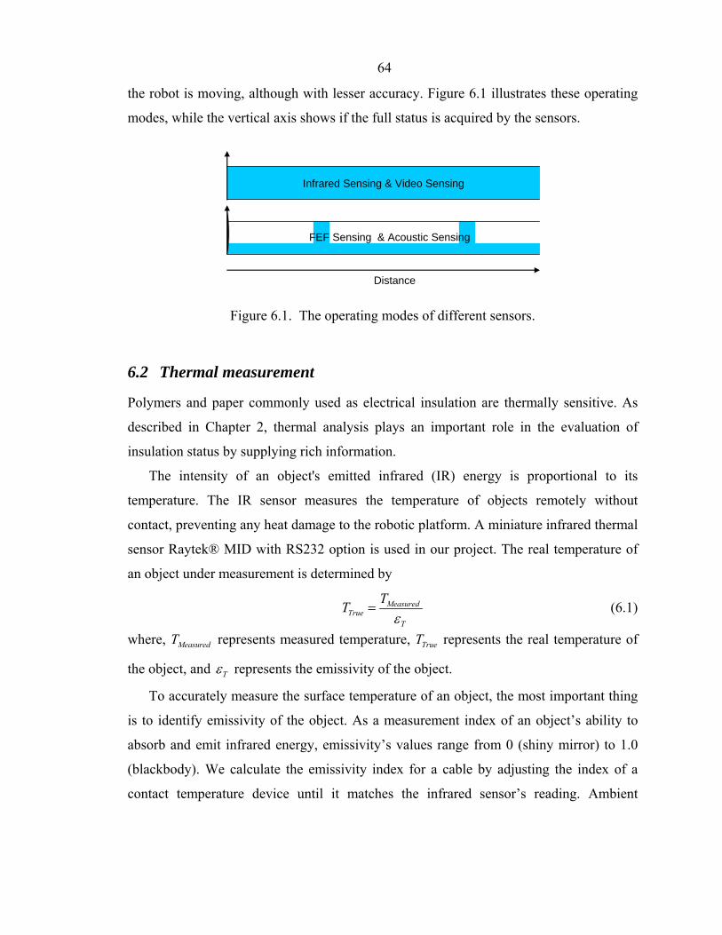
64
the robot is moving, although with lesser accuracy. Figure 6.1 illustrates these operating
modes, while the vertical axis shows if the full status is acquired by the sensors.
Infrared Sensing & Video Sensing
Distance
FEF Sensing & Acoustic Sensing
Figure 6.1. The operating modes of different sensors.
6.2 Thermal measurement
Polymers and paper commonly used as electrical insulation are thermally sensitive. As
described in Chapter 2, thermal analysis plays an important role in the evaluation of
insulation status by supplying rich information.
The intensity of an object's emitted infrared (IR) energy is proportional to its
temperature. The IR sensor measures the temperature of objects remotely without
contact, preventing any heat damage to the robotic platform. A miniature infrared thermal
sensor Raytek® MID with RS232 option is used in our project. The real temperature of
an object under measurement is determined by
MeasuredTrue
T
TTε
= (6.1)
where, MeasuredT represents measured temperature, TrueT represents the real temperature of
the object, and Tε represents the emissivity of the object.
To accurately measure the surface temperature of an object, the most important thing
is to identify emissivity of the object. As a measurement index of an object’s ability to
absorb and emit infrared energy, emissivity’s values range from 0 (shiny mirror) to 1.0
(blackbody). We calculate the emissivity index for a cable by adjusting the index of a
contact temperature device until it matches the infrared sensor’s reading. Ambient
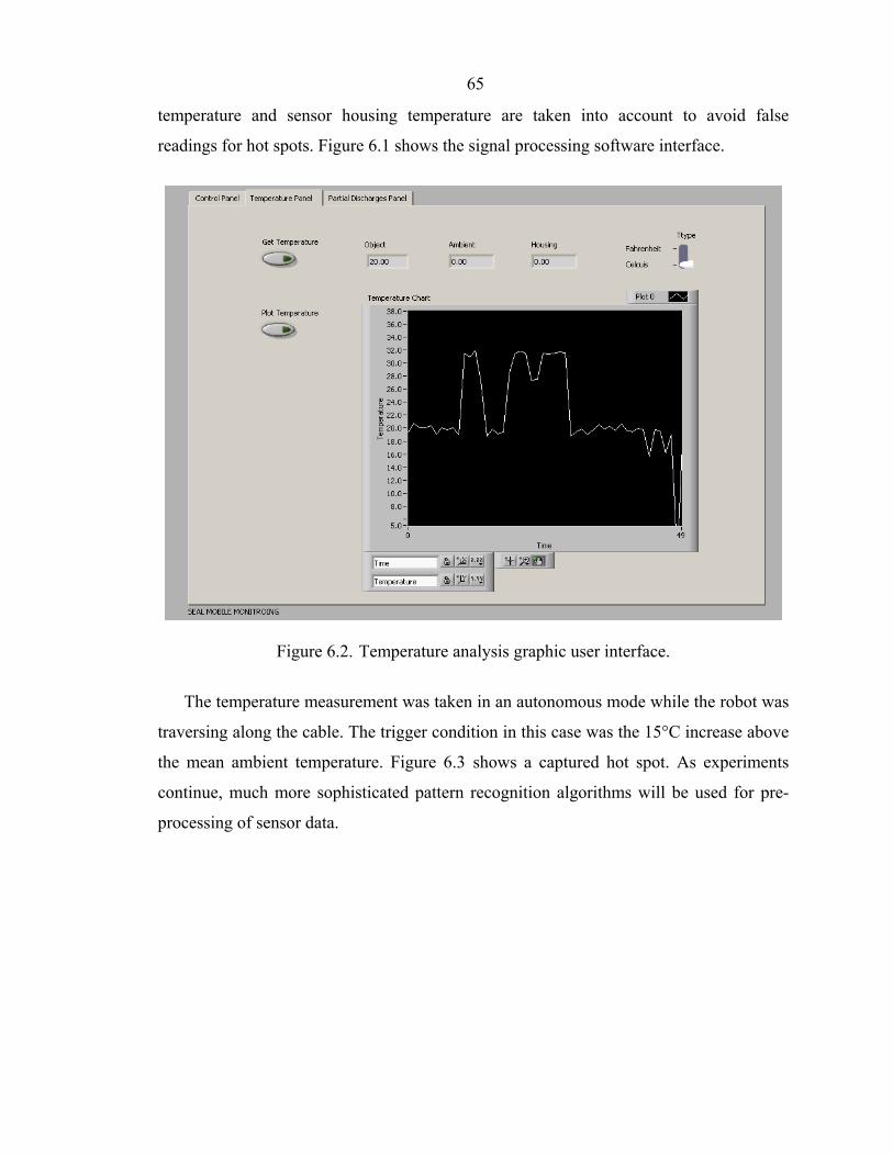
65
temperature and sensor housing temperature are taken into account to avoid false
readings for hot spots. Figure 6.1 shows the signal processing software interface.
Figure 6.2. Temperature analysis graphic user interface.
The temperature measurement was taken in an autonomous mode while the robot was
traversing along the cable. The trigger condition in this case was the 15°C increase above
the mean ambient temperature. Figure 6.3 shows a captured hot spot. As experiments
continue, much more sophisticated pattern recognition algorithms will be used for pre-
processing of sensor data.
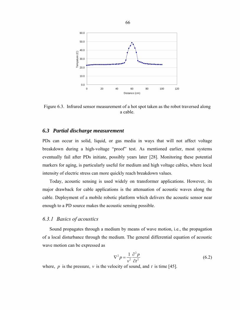
66
0.0
10.0
20.0
30.0
40.0
50.0
60.0
0 20 40 60 80 100 120
Distance (cm)
Tem
patu
re (C
)
Figure 6.3. Infrared sensor measurement of a hot spot taken as the robot traversed along a cable.
6.3 Partial discharge measurement
PDs can occur in solid, liquid, or gas media in ways that will not affect voltage
breakdown during a high-voltage “proof” test. As mentioned earlier, most systems
eventually fail after PDs initiate, possibly years later [28]. Monitoring these potential
markers for aging, is particularly useful for medium and high voltage cables, where local
intensity of electric stress can more quickly reach breakdown values.
Today, acoustic sensing is used widely on transformer applications. However, its
major drawback for cable applications is the attenuation of acoustic waves along the
cable. Deployment of a mobile robotic platform which delivers the acoustic sensor near
enough to a PD source makes the acoustic sensing possible.
6.3.1 Basics of acoustics
Sound propagates through a medium by means of wave motion, i.e., the propagation
of a local disturbance through the medium. The general differential equation of acoustic
wave motion can be expressed as
2
22 2
1 ppv t
∂∇ =
∂ (6.2)
where, p is the pressure, v is the velocity of sound, and t is time [45].

67
The elastic wave equation has a tensor form with three orthogonally polarized plane
wave solutions for any direction of propagation. The harmonic pressure wave equation
can be expressed as
( ) 0, sin xp x t p tv
ω ω⎛ ⎞= ±⎜ ⎟⎝ ⎠
(6.3)
This equation shows the variance of a pressure wave corresponding to time, location, and
velocity, angular velocity.
When a wave propagates through a structure, the wave’s intensity decreases as a
function of distance from the source. This phenomenon (called attenuation) results from
several mechanisms:
Geometrical spreading of the wave
Dividing of the wave among multiple paths
Transmission losses in propagation from one medium to another and at
discontinuities in the medium
Acoustic adsorption because of conversion of acoustic energy to heat [44].
When an acoustic wave propagates from one medium to another medium with
different acoustic impedance, reflection and refraction occur simultaneously. In the case
of normal incidence of a plane wave, the transmission coefficient is given by
( )
1 22
1 2
4trans
z zaz z
=+
(6.4)
where 1z and 2z represent two media’s acoustic impedance, and determined by
z vρ= (6.5) where ρ is the density of the specific medium. Equation (6.4) shows that only a small
fraction of the incident wave is transmitted across the interface if there is a large
difference in acoustic impedance; therefore a multi-layered structure, like a cable, will
greatly reduce the wave’s intensity.
A solid can support both longitudinal and transverse waves. Such waves are usually
generated simultaneously. Velocity, which differs for each wave type, can be determined
by the density and elastic properties of the material, i.e., Youngs modulus ( E ) and
Poisson ratio (μ ). In general, the velocity of a longitudinal wave is two times that of the
velocity of a transverse wave. For an unbounded solid, the velocity range is about
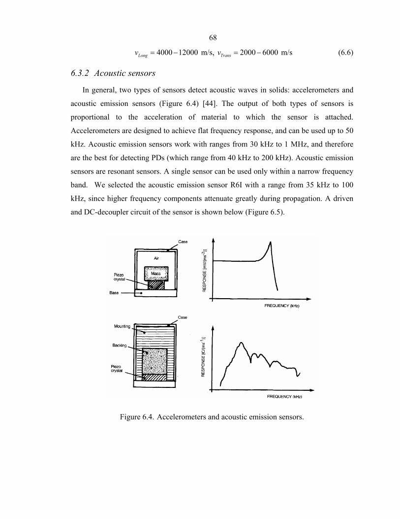
68
4000 12000Longv = − m/s, 2000 6000Transv = − m/s (6.6)
6.3.2 Acoustic sensors
In general, two types of sensors detect acoustic waves in solids: accelerometers and
acoustic emission sensors (Figure 6.4) [44]. The output of both types of sensors is
proportional to the acceleration of material to which the sensor is attached.
Accelerometers are designed to achieve flat frequency response, and can be used up to 50
kHz. Acoustic emission sensors work with ranges from 30 kHz to 1 MHz, and therefore
are the best for detecting PDs (which range from 40 kHz to 200 kHz). Acoustic emission
sensors are resonant sensors. A single sensor can be used only within a narrow frequency
band. We selected the acoustic emission sensor R6I with a range from 35 kHz to 100
kHz, since higher frequency components attenuate greatly during propagation. A driven
and DC-decoupler circuit of the sensor is shown below (Figure 6.5).
Figure 6.4. Accelerometers and acoustic emission sensors.
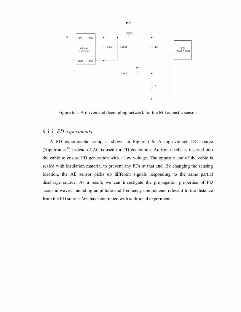
69
+15V
-15V
12V
GND
R6IBNC CONN
VoltageConverter
Vcc
To ADC
1uF
33m H
0.1uF 100uF 1uF
51
Figure 6.5. A driven and decoupling network for the R6I acoustic sensor.
6.3.3 PD experiments
A PD experimental setup is shown in Figure 6.6. A high-voltage DC source
(Hipotronics®) instead of AC is used for PD generation. An iron needle is inserted into
the cable to ensure PD generation with a low voltage. The opposite end of the cable is
sealed with insulation material to prevent any PDs at that end. By changing the sensing
location, the AE sensor picks up different signals responding to the same partial
discharge source. As a result, we can investigate the propagation properties of PD
acoustic waves, including amplitude and frequency components relevant to the distance
from the PD source. We have continued with additional experiments.
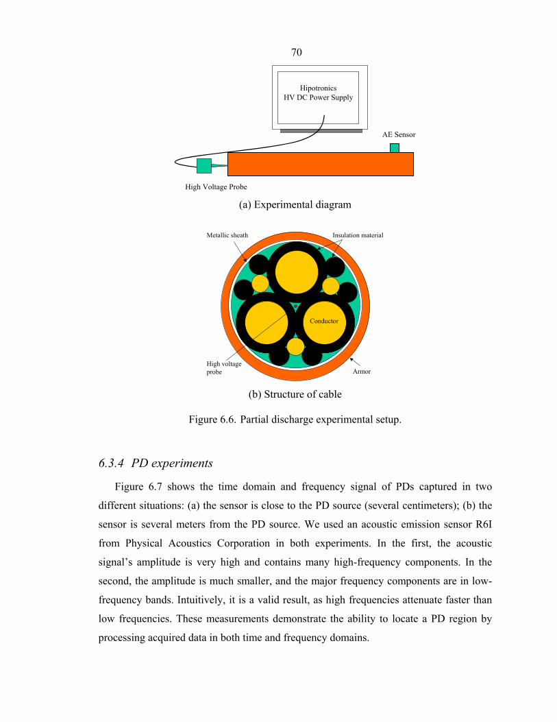
70
AE Sensor
High Voltage Probe
HipotronicsHV DC Power Supply
(a) Experimental diagram
Conductor
Insulation materialMetallic sheath
ArmorHigh voltageprobe
(b) Structure of cable
Figure 6.6. Partial discharge experimental setup.
6.3.4 PD experiments
Figure 6.7 shows the time domain and frequency signal of PDs captured in two
different situations: (a) the sensor is close to the PD source (several centimeters); (b) the
sensor is several meters from the PD source. We used an acoustic emission sensor R6I
from Physical Acoustics Corporation in both experiments. In the first, the acoustic
signal’s amplitude is very high and contains many high-frequency components. In the
second, the amplitude is much smaller, and the major frequency components are in low-
frequency bands. Intuitively, it is a valid result, as high frequencies attenuate faster than
low frequencies. These measurements demonstrate the ability to locate a PD region by
processing acquired data in both time and frequency domains.
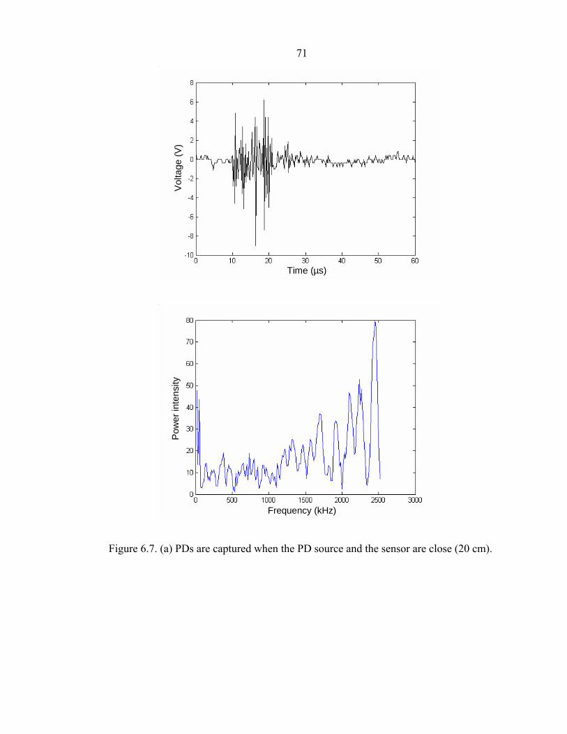
71
Time (µs)
Vol
tage
(V)
Frequency (kHz)
Pow
er in
tens
ity
Figure 6.7. (a) PDs are captured when the PD source and the sensor are close (20 cm).
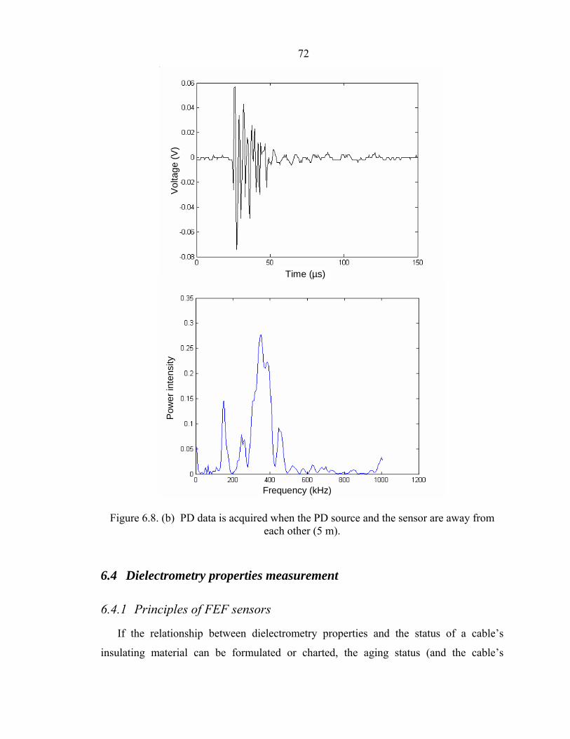
72
Time (µs)
Vol
tage
(V)
Frequency (kHz)
Pow
er in
tens
ity
Figure 6.8. (b) PD data is acquired when the PD source and the sensor are away from each other (5 m).
6.4 Dielectrometry properties measurement
6.4.1 Principles of FEF sensors
If the relationship between dielectrometry properties and the status of a cable’s
insulating material can be formulated or charted, the aging status (and the cable’s
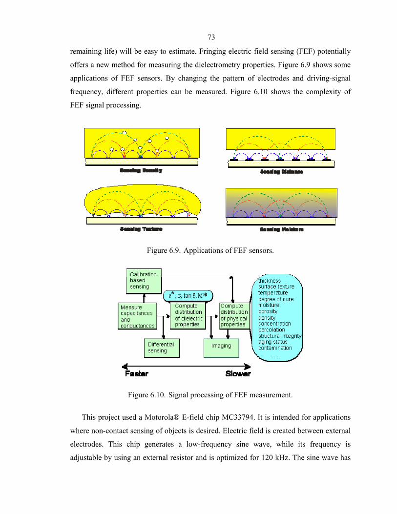
73
remaining life) will be easy to estimate. Fringing electric field sensing (FEF) potentially
offers a new method for measuring the dielectrometry properties. Figure 6.9 shows some
applications of FEF sensors. By changing the pattern of electrodes and driving-signal
frequency, different properties can be measured. Figure 6.10 shows the complexity of
FEF signal processing.
Figure 6.9. Applications of FEF sensors.
Figure 6.10. Signal processing of FEF measurement.
This project used a Motorola® E-field chip MC33794. It is intended for applications
where non-contact sensing of objects is desired. Electric field is created between external
electrodes. This chip generates a low-frequency sine wave, while its frequency is
adjustable by using an external resistor and is optimized for 120 kHz. The sine wave has
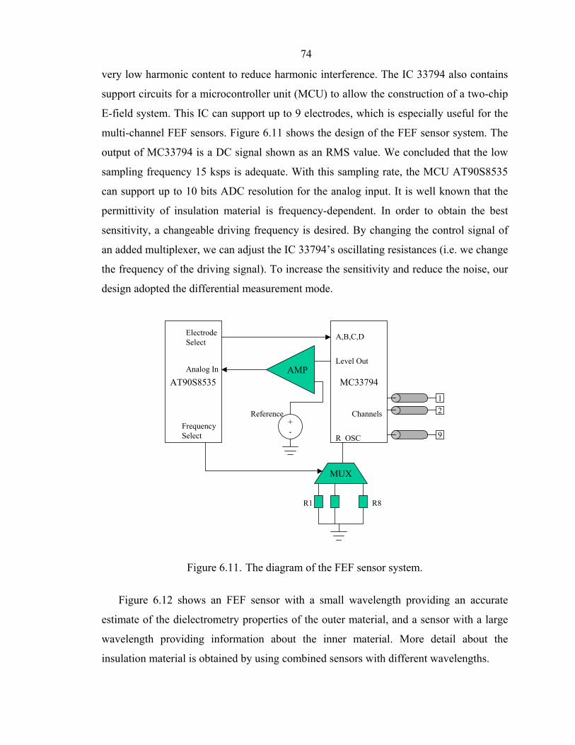
74
very low harmonic content to reduce harmonic interference. The IC 33794 also contains
support circuits for a microcontroller unit (MCU) to allow the construction of a two-chip
E-field system. This IC can support up to 9 electrodes, which is especially useful for the
multi-channel FEF sensors. Figure 6.11 shows the design of the FEF sensor system. The
output of MC33794 is a DC signal shown as an RMS value. We concluded that the low
sampling frequency 15 ksps is adequate. With this sampling rate, the MCU AT90S8535
can support up to 10 bits ADC resolution for the analog input. It is well known that the
permittivity of insulation material is frequency-dependent. In order to obtain the best
sensitivity, a changeable driving frequency is desired. By changing the control signal of
an added multiplexer, we can adjust the IC 33794’s oscillating resistances (i.e. we change
the frequency of the driving signal). To increase the sensitivity and reduce the noise, our
design adopted the differential measurement mode.
MC33794
12
9
AMPLevel Out
+-
Reference
AT90S8535
Electrode Select
Analog In
MUX
FrequencySelect
R1 R8
R_OSC
Channels
A,B,C,D
Figure 6.11. The diagram of the FEF sensor system.
Figure 6.12 shows an FEF sensor with a small wavelength providing an accurate
estimate of the dielectrometry properties of the outer material, and a sensor with a large
wavelength providing information about the inner material. More detail about the
insulation material is obtained by using combined sensors with different wavelengths.
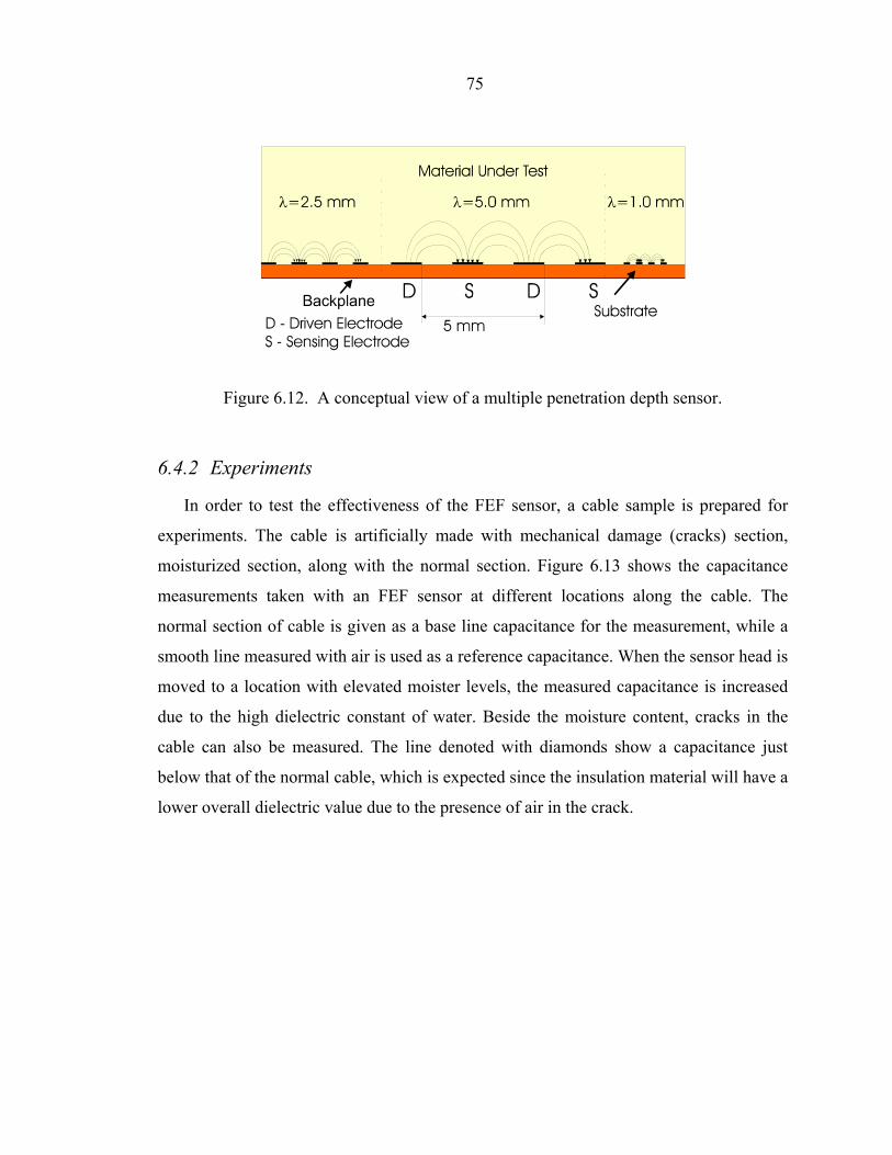
75
Figure 6.12. A conceptual view of a multiple penetration depth sensor.
6.4.2 Experiments
In order to test the effectiveness of the FEF sensor, a cable sample is prepared for
experiments. The cable is artificially made with mechanical damage (cracks) section,
moisturized section, along with the normal section. Figure 6.13 shows the capacitance
measurements taken with an FEF sensor at different locations along the cable. The
normal section of cable is given as a base line capacitance for the measurement, while a
smooth line measured with air is used as a reference capacitance. When the sensor head is
moved to a location with elevated moister levels, the measured capacitance is increased
due to the high dielectric constant of water. Beside the moisture content, cracks in the
cable can also be measured. The line denoted with diamonds show a capacitance just
below that of the normal cable, which is expected since the insulation material will have a
lower overall dielectric value due to the presence of air in the crack.

76
Frequency (Hz)
Cap
acita
nce
(pF)
102
103
104
105
26
26.5
27
27.5
28
28.5
29
29.5
30AirNormal CableDamage CableWet Cable
Figure 6.13. FEF experimental results to samples with different status.
6.5 Conclusions
In this chapter, the working principles and experimental setups for the infrared sensor, the
acoustic sensor, and the fringing electric field sensor are described. A temperature
processing algorithm and graphic interface are developed. Based on the acoustic
properties of partial discharges, an acoustic emission sensor is chosen and a
corresponding driving circuit is designed. A simplified experiment setup for partial
discharges is presented. Finally, the fringing electric field sensor system based on the
MC33794 E-field chip is designed to detect dielectric properties.

77
Chapter 7. Energy Scavenging Issues for Passive RFIDs
7.1 Introduction
The notion of a low-cost, ubiquitous device that combines sensing and wireless radio
capability based on RFID principles was proposed as an alternative to current wireless
sensor networks [86]. Figure 7.1 shows the system configuration that integrates an RFID
tag IC and a MEMS/CMOS sensor for potential applications, such as temperature
monitoring and motion detection. There are active, passive, and semi-passive RFID tags.
Passive RFID tags are of special interest due to the absence of power supply, implying
low cost and longevity. During read interrogation, passive RFID tags obtain and store the
impinging energy that is used to power the tag’s IC. Because the tags’ operating range is
limited by the availability of energy, the fundamentals of energy scavenging practices
must be thoroughly understood to make optimum use of such tags.

78
Impedance Matching
Unit
Rectifier/Voltage Amplification Unit
Demod-ulator
Clock
Control/Encoder
Logic
A/D
I/O Port
CMOS/MEMS Sensor
I/O Port
DSP
Modulation/Demodulation
Transceiver
Rec
eivi
ng
Transmitting
Power
ID & Sensing
Host ComputerVoltage
Regulator
Reader Tag
Figure 7.1. The RFID reader-tag system.
7.2 Energy scavenging considerations
A power scavenging circuitry in the RFID tag harvests the incoming RF power via the
antenna, and converts it to DC power. The minimum output voltage required to enable
the tag IC to work can be 1.8 V, 1.2 V, or even a lower voltage depending on the CMOS
fabrication process. The tag IC can be treated as an equivalent resistive load ldR . For a
specified load ldR , either the output power outP or the DC output voltage outV can be used
to represent the output power, since
2
outout
ld
VPR
= (7.1)
Different operating situations and fabrication processes affect ldR . In order to accurately
express the relationship between outP ( outV ) and ldR , the power conversion efficiency η
is introduced as
2
out out
in ld in
P VP R P
η = = (7.2)
where inP is the input power, and is affected by mismatching and the dissipation by the
rectifier circuit. We considered the effect of varying ldR to outV and outP , and observed
the following results (Figure 7.2):

79
• outV increases with increasing ldR , and converges to the maximum value.
• η increases with increasing ldR until it reaches its maximum, and then it
decreases with increasing ldR .
The performance of different scavenging circuits varies, but they all follow these rules.
For a specified ldR , the harvested energy must meet the minimal output voltage to
guarantee the tag’s operation. Usually, the worst case (the smallest ldR ) is selected for
design considerations. A design challenge for our project was to select a circuit that
offers the best performance.
ldR
outV
Maximum output Voltage
Minimum working output Voltage
ldR
Maximum efficiency
η
MaxldR
Figure 7.2. The relationship between the output voltage/power and the equivalent load

80
7.3 Working principles
Most passive RFID systems operate in UHF frequency band (860~960 MHz) or HF
frequency band (13.56 MHz). Some systems operate in LF band (120 kHz), UHF band
(2.45 GHz), or SHF band(5.8 GHz) [69]. The frequency difference leads to different
working principles: the HF RFID uses magnetic coupling so the reader and tag antennas
could be treated as a weakly coupled transformer; the UHF RFID uses electromagnetic
coupling, where the RFID tag usually has little effect on the impedance of the reader’s
antenna. However, the energy harvesting process is identical for both frequency bands:
the incident power emitted from the reader antenna is partially captured by the tag
antenna ( rP ), while the remaining power ( reP ) is partially dissipated as heat loss and
partially reflected into the air. Part of the captured power ( inP ) is rectified to a DC source
to drive the tag’s IC, and the rest is dissipated due to the insertion loss of the rectifier
circuit and the leakage. Below, we describe some of the technical issues involved in
improving the efficiency of the harvested energy at the tag.
7.3.1 Power transmission
For the UHF frequency band, when the tag is working in the far field of the reader’s
antenna (the distance is relatively large compared to the wavelength and the dimensions
of the antenna), rP is written as the Friis transmission formula [87]
2 2et er
r tA AP Pd λ
= (7.3)
where 2
( ) 4et erA G λπ
= is the effective aperture of the transmitting antenna or receiving
antenna; d is the distance between two antennas; λ is the wavelength of the specified
frequency; tP is the emitted power of the transmitting antenna; and G is the antenna’s
gain. In the UHF band, tP is regulated strictly (1 W in USA or 0.5 W in Europe).
Antennas that can cover the desired workspace in specified applications do not give
designers much room on the antenna’s gain, so improvement on rP is very limited.
In the HF frequency band, the loop antennas of the reader and the tag are weakly
coupled. In the far field, rP can be written as
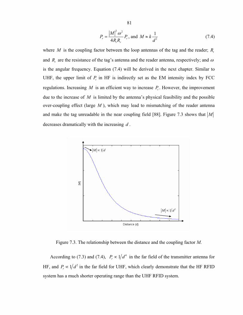
81
2 2
4r tt r
MP P
R Rω
= , and 2
1M kd
≈ (7.4)
where M is the coupling factor between the loop antennas of the tag and the reader; tR
and rR are the resistance of the tag’s antenna and the reader antenna, respectively; and ω
is the angular frequency. Equation (7.4) will be derived in the next chapter. Similar to
UHF, the upper limit of tP in HF is indirectly set as the EM intensity index by FCC
regulations. Increasing M is an efficient way to increase tP . However, the improvement
due to the increase of M is limited by the antenna’s physical feasibility and the possible
over-coupling effect (large M ), which may lead to mismatching of the reader antenna
and make the tag unreadable in the near coupling field [88]. Figure 7.3 shows that M
decreases dramatically with the increasing d .
1M d∝
21M d∝
Figure 7.3. The relationship between the distance and the coupling factor M.
According to (7.3) and (7.4), 41rP d∝ in the far field of the transmitter antenna for
HF, and 21rP d∝ in the far field for UHF, which clearly demonstrate that the HF RFID
system has a much shorter operating range than the UHF RFID system.

82
7.3.2 Impedance matching network
When designing RF circuitry, impedance matching is necessary to provide the
maximum power delivery between a source and its load and to improve the signal-to-
noise ratio [89]. Various matching networks are shown in Figure 7.4, where sZ is the
source impedance, LZ is the load impedance, iZ is the impedance of the reactive
matching element, and sV is the induced voltage of the antenna. When compared with the
simplest L network, the T and π networks are best suited for high-Q (narrow-band)
matching, and the wideband network for the low-Q (wideband) matching. Network
selection depends on the design and cost considerations.
Figure 7.4. The impedance matching circuits.
The load ldR after the rectifier is that we concern (Figure 7.5), not the load LZ across
the rectifier input terminals (Figure 7.4). Since a diode or a MOSFET is a nonlinear
device, we speculated that the maximum power delivered to LZ cannot guarantee the
maximum power delivered to ldR . Simulation results confirmed our speculation. Due to
the complexity of the rectifier circuit (such as leakage and reverse biased conditions),
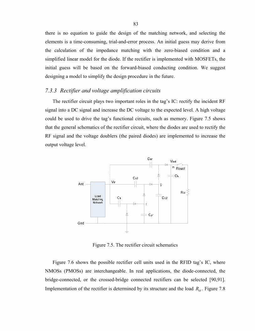
83
there is no equation to guide the design of the matching network, and selecting the
elements is a time-consuming, trial-and-error process. An initial guess may derive from
the calculation of the impedance matching with the zero-biased condition and a
simplified linear model for the diode. If the rectifier is implemented with MOSFETs, the
initial guess will be based on the forward-biased conducting condition. We suggest
designing a model to simplify the design procedure in the future.
7.3.3 Rectifier and voltage amplification circuits
The rectifier circuit plays two important roles in the tag’s IC: rectify the incident RF
signal into a DC signal and increase the DC voltage to the expected level. A high voltage
could be used to drive the tag’s functional circuits, such as memory. Figure 7.5 shows
that the general schematics of the rectifier circuit, where the diodes are used to rectify the
RF signal and the voltage doublers (the paired diodes) are implemented to increase the
output voltage level.
Figure 7.5. The rectifier circuit schematics
Figure 7.6 shows the possible rectifier cell units used in the RFID tag’s IC, where
NMOSs (PMOSs) are interchangeable. In real applications, the diode-connected, the
bridge-connected, or the crossed-bridge connected rectifiers can be selected [90,91].
Implementation of the rectifier is determined by its structure and the load ldR . Figure 7.8

84
shows how the load and stage number of the rectifier can affect the output voltage. A
detailed discussion on the rectifier design appears in Chapter 9.
Figure 7.6. The rectifier circuit cell units.
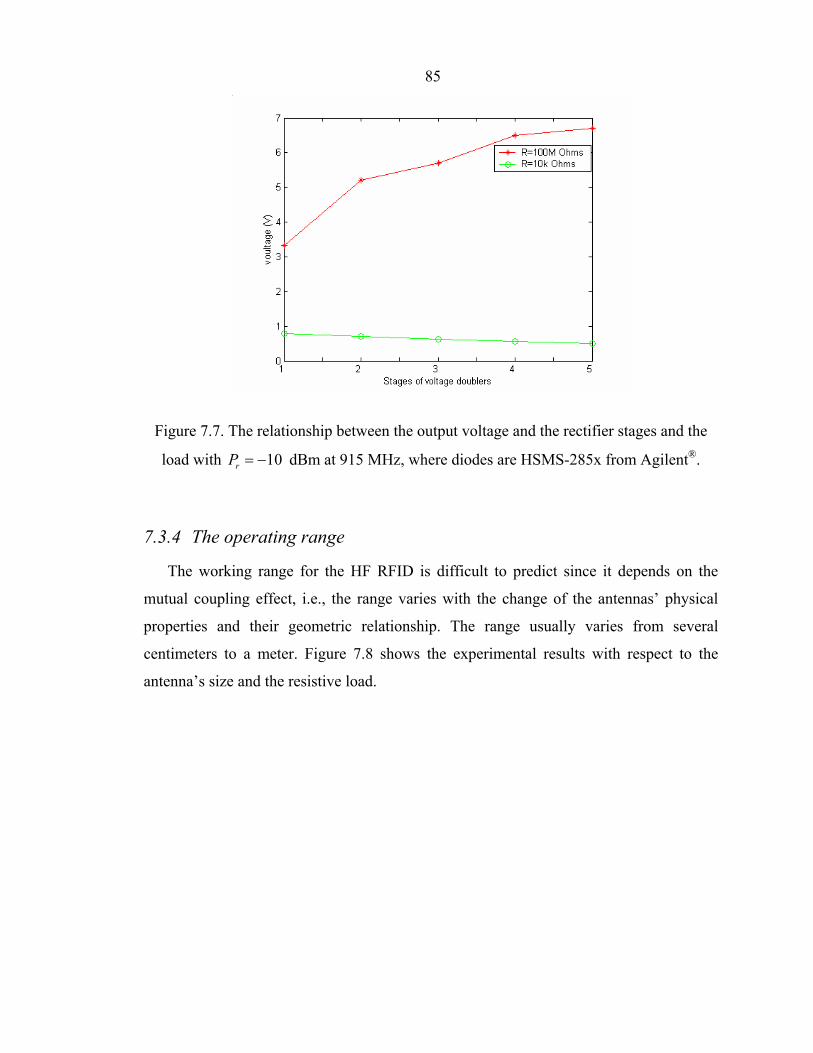
85
Figure 7.7. The relationship between the output voltage and the rectifier stages and the
load with 10rP = − dBm at 915 MHz, where diodes are HSMS-285x from Agilent®.
7.3.4 The operating range
The working range for the HF RFID is difficult to predict since it depends on the
mutual coupling effect, i.e., the range varies with the change of the antennas’ physical
properties and their geometric relationship. The range usually varies from several
centimeters to a meter. Figure 7.8 shows the experimental results with respect to the
antenna’s size and the resistive load.
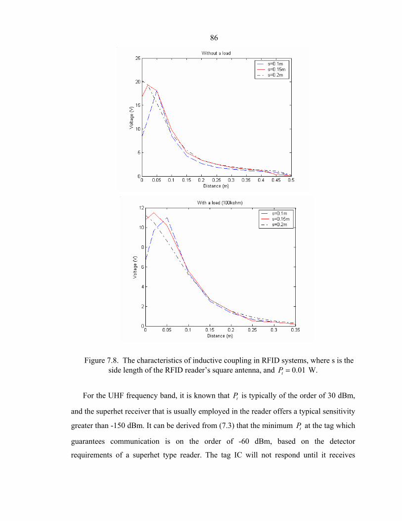
86
Figure 7.8. The characteristics of inductive coupling in RFID systems, where s is the side length of the RFID reader’s square antenna, and 0.01tP = W.
For the UHF frequency band, it is known that tP is typically of the order of 30 dBm,
and the superhet receiver that is usually employed in the reader offers a typical sensitivity
greater than -150 dBm. It can be derived from (7.3) that the minimum tP at the tag which
guarantees communication is on the order of -60 dBm, based on the detector
requirements of a superhet type reader. The tag IC will not respond until it receives

87
enough power from the reader. The reported minimum required tP is about -10 to -16
dBm which far exceeds -60 dBm. Therefore, the reader sees a detectable tag response
signal as long as the interrogating power at the tag exceeds the minimum required power.
The maximum range for a specified UHF RFID system can be calculated as
( )
2
24t
et erld
Pd G GP
ληπ
= , (7.5)
where ld
r
PP
η = is the power efficiency; etG is the gain of the reader’s antenna; and etG
and erG are the gain of the reader’s antenna and the gain of tag’s antenna, respectively.
Figure 7.9 predicts the relationship between the work range and the received power.
Figure 7.10 demonstrates the experimental relationship between the output voltage and
the distance, which is consistent with the theoretical prediction. Due to the near field
effect, the output voltage in the experiments is higher than the value predicted by the Friis
equation.
Figure 7.9. Relationship between received power and distance (transmitted power = 30 dBm, reader antenna gain = 4, and tag antenna gain = 1).
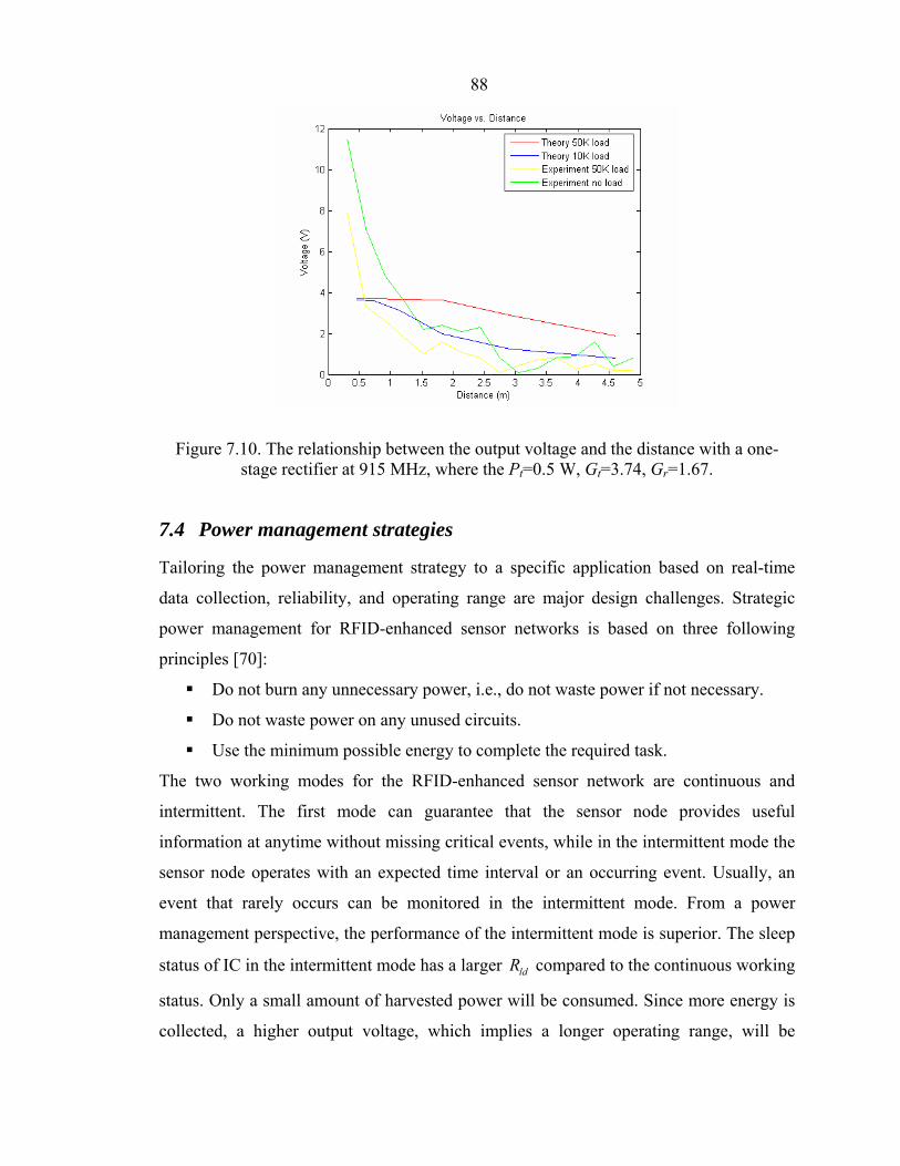
88
Figure 7.10. The relationship between the output voltage and the distance with a one-stage rectifier at 915 MHz, where the Pt=0.5 W, Gt=3.74, Gr=1.67.
7.4 Power management strategies
Tailoring the power management strategy to a specific application based on real-time
data collection, reliability, and operating range are major design challenges. Strategic
power management for RFID-enhanced sensor networks is based on three following
principles [70]:
Do not burn any unnecessary power, i.e., do not waste power if not necessary.
Do not waste power on any unused circuits.
Use the minimum possible energy to complete the required task.
The two working modes for the RFID-enhanced sensor network are continuous and
intermittent. The first mode can guarantee that the sensor node provides useful
information at anytime without missing critical events, while in the intermittent mode the
sensor node operates with an expected time interval or an occurring event. Usually, an
event that rarely occurs can be monitored in the intermittent mode. From a power
management perspective, the performance of the intermittent mode is superior. The sleep
status of IC in the intermittent mode has a larger ldR compared to the continuous working
status. Only a small amount of harvested power will be consumed. Since more energy is
collected, a higher output voltage, which implies a longer operating range, will be

89
generated by the power scavenging circuit when the sensor node works in the intermittent
mode.
In summary, the sensor node that works in the intermittent mode offers the longer
operating range that is more suited to the distribution network applications. The power
scavenging circuit should be optimized with a larger ldR if possible to harvest the energy
necessary for the full-function operations of tags.
7.5 Conclusions
Energy scavenging is one of the most important issues in RFID and RFID-enhanced
sensor design. It enables operation and enhances the spatial range of individual nodes.
We discussed the working principles and causative factors, and investigated power
management strategies that would improve performance.

90
Chapter 8. Energy Scavenging for Inductively Coupled Passive
RFIDs
8.1 Introduction
This chapter investigates energy scavenging for inductively coupled passive HF RFID
systems and studies how mutual inductance between the reader and the tag affects the
amount of power generated at the tag. HF RFID uses magnetic waves in the antenna near
field to communicate. Because the magnetic field is not affected by most of surrounding
dielectric materials ( 1rμ ≈ ), HF RFID has good performance in a crowded environment
and presents a viable solution for energy scavenging in our applications. In order to
pursue the maximum operating range, the maximum power transfer efficiency from the
RFID reader to the tag must be ensured. The reader antenna and the tag antenna are
mutually coupled by the magnetic field. Mutual coupling can be viewed as a load at the
reader antenna. This presents a challenge since the reader must handle a changing
effective load due to
The location-dependent mutual coupling effect between the reader antenna and
the tag antenna
The unpredictable number of tags in the read zone of the reader antenna
This load may lead to impedance mismatch and poor power transfer efficiency if a fixed
impedance-matching circuit is implemented for the reader antenna; accordingly, an
adaptive impedance-matching network at the reader is proposed. We offer guidelines for
the design of the antenna to improve the power transfer from the reader to the tags.

91
8.2 Working mechanism
8.2.1 L-Matching
As we discussed in Section 7.3.2, there are different types of matching networks (Figure
7.4). In this application, the L-matching network is selected due to its simple structure
and easy tuning. Figure 8.1 shows the lumped circuits of the loop antenna only (left) and
the loop antenna with the L-match network (right), where 1X and 2X are reactive
elements for the matching purpose, and ANTR and ANTL are the resistance and self-
inductance of the antenna. Figure 8.1 is valid only when ANT ANT srR j L Rω+ > , where srR
is the source (generator) resistance [92]. Thus, the impedance of an inductive antenna is
matched to the source impedance as
( ) 12
1
ANT ANTsr
ANT ANT
R j L jXjX R
R j L jXωω
++ =
+ + (8.1)
where ω is the angular frequency. Due to the skin effect, the resistive loss ANTR in (8.1)
can be expressed as
2ANTl fRw
π μσ
≈ (8.2)
where σ and μ are the conductor’s electrical conductivity and magnetic permeability, l
is the length of the loop, w is the trace width, and f is the signal frequency [93].
ANTL
ANTR
ANTL
ANTR
1jX
2jX
Figure 8.1. L-matching network (left: original antenna; right: matched antenna).
It is difficult to accurately estimate ANTL in (8.1), especially for a planar coil. For a round planar spiral coil, ANTL can be roughly approximated by (8.3) with at least 80% accuracy [94]

92
2
231.338 11ANT
aL Na c
μ≈+
(8.3)
where N is the number of turns in the loop, a is the coil mean radius, and c is the
thickness of the winding. Analytical expressions for planar rectangular coils are available
in [95]. Their accurate values can be approximated with numerical EM simulation
software, such as HFSS® or Sonnet®. When the resistance and inductance of the loop are
determined, 1X and 2X can be solved by using (8.1).
8.2.2 Induced magnetic field
A changing current along a conductor loop induces a changing magnetic field. When
another conductor loop is placed in this field, an induced voltage is generated along the
loop. To simplify the calculation of the magnetic field, the inductive loop can be treated
as a series of small dipoles. Figure 8.2 shows an electric dipole model. The magnetic field
in the vicinity of the dipole is expressed as
02 22
j tI her r h
ωμπ
≈+
B (8.4)
where h is the half-length of the dipole, 0I is the current amplitude along the dipole, μ
is the permeability of air, and r is the distance from P to the center of the dipole [87].
r
Bα P
O
zx
y
h
hθ
Figure 8.2. Magnetic field generated by an electric dipole.

93
Based on (8.4), the magnetic field along the central axis x generated by a rectangular
inductive loop antenna can be expressed as
0xB KI= (8.5)
2 2 2 22 2 21
1 1rni i
i i ii i
a bKa x b xa b x
μπ =
⎛ ⎞≈ +⎜ ⎟+ ++ + ⎝ ⎠
∑ (8.6)
where xB is the amplitude of the magnetic field component along the x axis, ia and ib
are the half side-length of the rectangular loop, and rn is the number of turns.
8.2.3 Induced voltage
When a loop is placed in the magnetic field, the induced voltage generated is
calculated as
t C SV d d
t∂
= ⋅ = − ⋅∂∫ ∫E l B s (8.7)
where C is the length of the loop curve, S is the area of the loop, E is the electric field
vector, l is the tangent direction of the loop curve, and s is the normal direction of the
loop surface. The RFID tag is usually small, and so B is treated as a constant at the tag
location. Because the induced voltage from each turn is serially connected, for a tag with
a tn turn antenna, the induced voltage is
01 1
t tn n
t i ii i
V j B S j I K Sω ω= =
≈ − = −∑ ∑ (8.8)
Equation (8.8) shows that tV can vary by adjusting design parameters, such as the
number of turns and the dimension of the loop. This approximation assumes that the
magnetic field generated by the tag in the direction opposite to the magnetic field
generated by the reader is negligible, i.e. 0I is treated as a constant. When the reader
antenna and the tag antenna are far apart, this assumption usually holds true. However, it
cannot be used to predict the output voltage when the tag works in the near field of the
reader antenna, since 0I is forced to change in this case. In order to reach optimum power
delivery performance, the accurate estimations of 0I and tV are required.

94
8.3 Loading effect
The induced voltage on the tag generates current along the tag loop antenna, following an
EM field in the direction opposite to the triggering EM field. The reader antenna and the
tag antenna can be treated as a pair of weakly coupled transformers, as shown in Figure
8.3 with a coupling factor M [96]. Therefore, the induced voltage at the tag can also be
derived as
0tV j MIω= (8.9)
According to (8.8), the coupling coefficient is determined as
1
tn
ii
M K S=
= − ∑ (8.10)
Equation (8.10) shows that M is only determined by the geometry and the relative
position of the two antennas.
Switch
Reader Tag
Z MatchingNetwork
&Rectifiercircuit
srR 2jX
1jX
rR
rL MtL
tR
tV
ldZpV
0I tI01
0010
11
Figure 8.3. The circuit schematics of the coupled RFID reader antenna and tag antenna.
Based on the KVL and KCL, we derived the following equations for an RFID reader
antenna when it is loading tags and is matched with an L-matching network:
( )
2
01
0
p sr r
r
r r r t
V R I Z I V
VI IZ
V R j L I j MIω ω
⎧ = + +⎪⎪ = +⎨⎪⎪ = + +⎩
(8.11)
where srR is the source resistance; rR and rL are the resistance and inductance of the
reader antenna, respectively; pV and rV are the driving source voltage and voltage at the

95
reader antenna, respectively; I , 0I , and tI are the currents flowing through srR , the
reader antenna, and the tag antenna, respectively; and 1 1Z jX= and 2 2Z jX= are the
impedances of the matching elements.
Using KVL for the tag circuit yields
( )0 0t t t t tj MI R j L I Z Iω ω+ + + = (8.12)
where tR and tL are the tag resistance and inductance, and tZ is the tag IC impedance at
the port 00-01, including the matching network, rectifier, and load impedance ldZ , as
shown in Figure 8.3. The induced voltage on the tag is rectified and fed to the load.
Figure 7.5 depicts the rectifier circuit. More discussion of the rectifier design is in
Chapter 9.
If the loss is negligible, maximum output power can be reached at the tag when the
tag IC impedance tZ is matched to the source impedance ( t tR j Lω+ ), i.e.
t t tZ R j Lω= − (8.13)
Therefore, the tag current tI is given by
01
2tt
I j MIR
ω= − (8.14)
Replacing tI in (8.11) by using (8.14), 0I is expressed as
( )( )
( )221 1 1
0211
21
2 22psr r r
t r r srsr r r
VR R j L Z Z M ZIR R j L Z RR R j L Z
ω ωωω
⎛ ⎞⎛ ⎞+ + +⎜ ⎟+ =⎜ ⎟
⎜ ⎟⎜ ⎟ + ++ +⎝ ⎠⎝ ⎠ (8.15)
Here, 0I is still unsolved since rL and 1Z remain unknown. When the unloaded reader
loop antenna ( 0M = ) is matched to its source resistance srR , the power dissipated by the
antenna is
2 21 1
2 2 2 8p p
ANTsr sr
V VP
R R⎛ ⎞
= =⎜ ⎟⎜ ⎟⎝ ⎠
(8.16)
Since passive elements do not dissipate power, ANTP is the power dissipated by rR , i.e.,
0 _ 2p sr
unloadsr r
V RIR R
= (8.17)
When 0M = , 0I can also be derived from (8.11) as

96
10_
12p
unloadsr r r
V ZIR R j L Zω
=+ +
(8.18)
Referring to (8.17), 1
1r r
ZR j L Zω+ +
can be rewritten as
1
1
jsr
r r r
RZ eR j L Z R
ϑ
ω=
+ + (8.19)
where ϑ is the phase. Introducing (8.19) into (8.15), (8.15) is rewritten as
( ) ( )22 2
1 011
2 2 2j pj jsr sr
r r t r sr
VMR RC e e I eR R R R R
ϑ π ϑ ϑωω +
⎛ ⎞⎛ ⎞+ + =⎜ ⎟⎜ ⎟⎜ ⎟⎜ ⎟⎝ ⎠⎝ ⎠
(8.20)
Since 1Cω and ϑ are usually small, this equation can be simplified as
( )12
011
2 4psr
r sr r t
V MRIR R R R
ω−
⎛ ⎞≈ +⎜ ⎟
⎜ ⎟⎝ ⎠
(8.21)
Based on (8.16), the harvested power TP on the RFID tag IC is
( )21
21 118 2 4
psrT
t r sr r t
VRP M MR R R R R
ω ω−
⎛ ⎞≈ +⎜ ⎟
⎝ ⎠ (8.22)
8.4 Discussion
Equation (8.22) shows that TP has a nonlinear relationship with the mutual coupling
factor M . Figure 8.4 plots this relationship, where the reader antenna has 0.2 0.2S = ×
m2 area and one turn, a tag antenna has 0.023S = m2 area and 10 turns, tR = 6.2 Ω , pV =
5 V, and srR = 50 Ω . The complex relationship between TP and M can be simplified in
two scenarios:
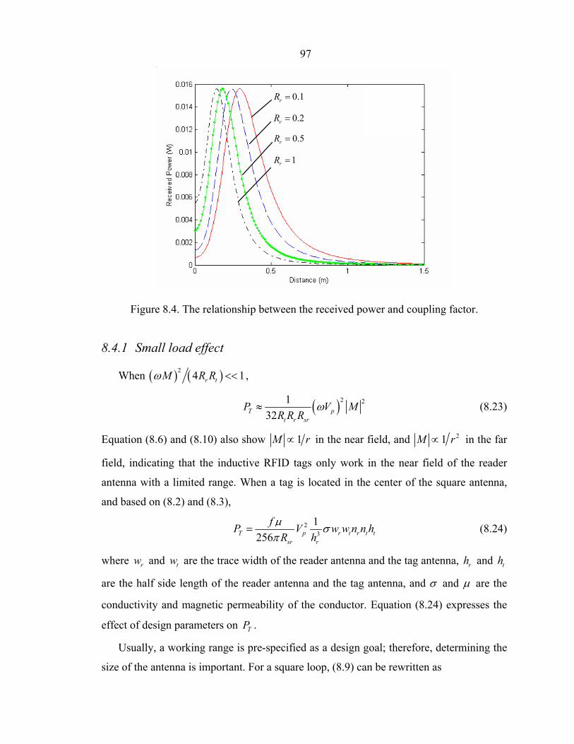
97
0.1rR =
0.2rR =
0.5rR =
1rR =
Figure 8.4. The relationship between the received power and coupling factor.
8.4.1 Small load effect
When ( ) ( )2 4 1r tM R Rω << ,
( )2 2132T p
t r sr
P V MR R R
ω≈ (8.23)
Equation (8.6) and (8.10) also show 1M r∝ in the near field, and 21M r∝ in the far
field, indicating that the inductive RFID tags only work in the near field of the reader
antenna with a limited range. When a tag is located in the center of the square antenna,
and based on (8.2) and (8.3),
23
1256T p r t r t t
sr r
fP V w w n n hR hμ σπ
= (8.24)
where rw and tw are the trace width of the reader antenna and the tag antenna, rh and th
are the half side length of the reader antenna and the tag antenna, and σ and μ are the
conductivity and magnetic permeability of the conductor. Equation (8.24) expresses the
effect of design parameters on TP .
Usually, a working range is pre-specified as a design goal; therefore, determining the
size of the antenna is important. For a square loop, (8.9) can be rewritten as

98
( )
2
0 2 2 2 22t
hV kd h d h
=+ +
(8.25)
where 0k is a constant, and d is the expected range. If 0tdV dh = , we obtain the
optimum half side length of the loop
( )1 1 52
h d= + (8.26)
For a circular loop, the dipole can be approximated as
2
h θγ Δ≈ (8.27)
where γ is the radium of the circular loop, and θ is the sector angle to the cord 2h , as
shown in Figure 8.1. xB and tV can be expressed as
( ) ( )
2 22
3 2 3 20 2 2 2 22xB d
d r d r
π γ πγθ= =+ +
∫ (8.28)
( ) 3 22 2 20tV k dπγ γ
−= + (8.29)
When 0tdV dγ = , we obtain the optimum radius of the loop
2dγ = (8.30)
8.4.2 Large load effect
When ( ) ( )2 4 1r tM R Rω > ,
222
t rT p
sr
R RP VM Rω
≈ (8.31)
TP decreases as the coupling factor M increases, because a larger coupling gives a
smaller 0I . Two possible situations may result in a large load effect: many tags within the
reader’s operating range, or a closely located tag. When a tag is moved closely to the
reader, the output voltage may increase gradually until it peaks and then drops. In other
words, a relatively large coupling effect could lower the power transfer between the
reader and the tag.
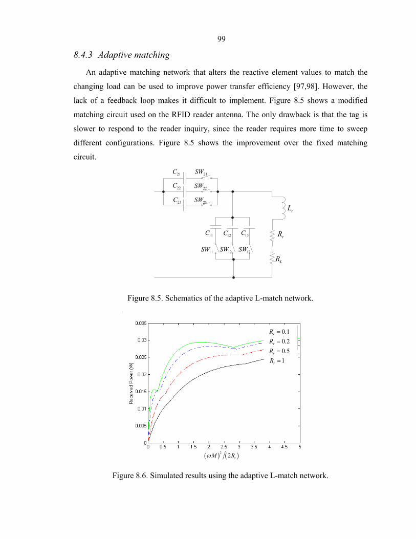
99
8.4.3 Adaptive matching
An adaptive matching network that alters the reactive element values to match the
changing load can be used to improve power transfer efficiency [97,98]. However, the
lack of a feedback loop makes it difficult to implement. Figure 8.5 shows a modified
matching circuit used on the RFID reader antenna. The only drawback is that the tag is
slower to respond to the reader inquiry, since the reader requires more time to sweep
different configurations. Figure 8.5 shows the improvement over the fixed matching
circuit.
rL
rR
LR
21C
22C
23C
21SW
22SW
23SW
11C 12C 13C
11SW 12SW 13SW
Figure 8.5. Schematics of the adaptive L-match network.
( ) ( )2 2 tM Rω
0.1rR =0.2rR =0.5rR =1rR =
Figure 8.6. Simulated results using the adaptive L-match network.

100
Based on the maximum power transfer with impedance matching, the power received
by the tag when using the fixed matching algorithms shows a maximum value of 12.5%
of ( ) 12 8p srV R − which is the total power consumed. Figure 8.6 shows the maximum power
efficiency for the complete adaptive matching network can be reached at 25%.
8.5 Experimental results
We designed a tag loop antenna with 15-turns, 46× 46 mil2 outer dimensions, 0.254 mm
gap, and 0.254 mm track width. We used a voltage doubler to raise the output voltage.
Figure 8.7, Figure 8.8, and Figure 8.9 show the results with pV = 3 V, where x axis is the
distance between the centers of the two antennas, and y axis is the output voltage
generated on the tag.
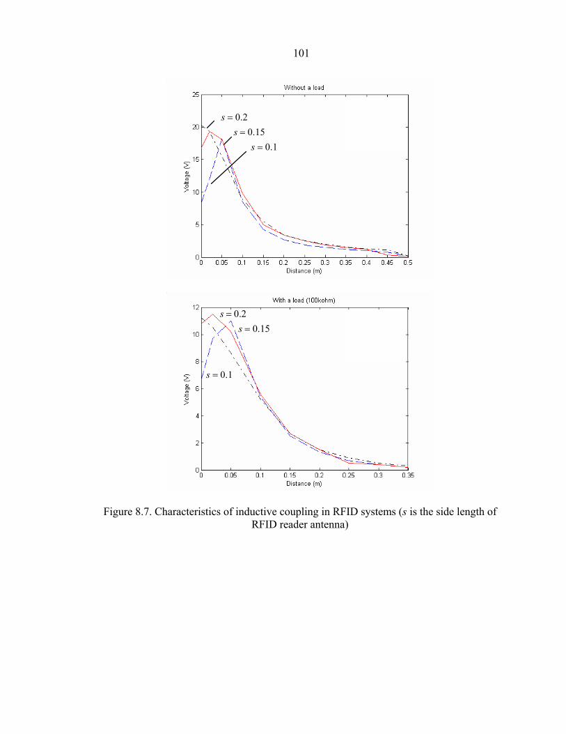
101
0.2s =0.15s =
0.1s =
0.2s =0.15s =
0.1s =
Figure 8.7. Characteristics of inductive coupling in RFID systems (s is the side length of RFID reader antenna)
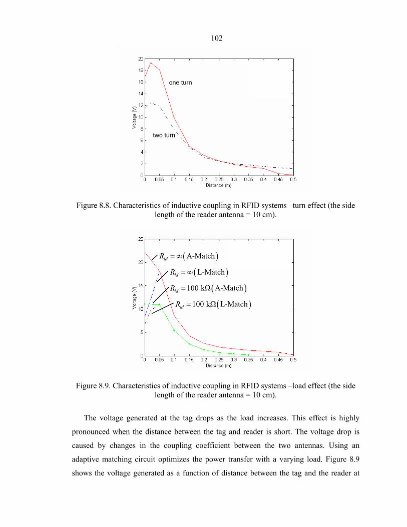
102
one turn
two turn
Figure 8.8. Characteristics of inductive coupling in RFID systems –turn effect (the side length of the reader antenna = 10 cm).
( )L-MatchldR = ∞
( )A-MatchldR = ∞
( )100 kΩ L-MatchldR =
( )100 kΩ A-MatchldR =
Figure 8.9. Characteristics of inductive coupling in RFID systems –load effect (the side length of the reader antenna = 10 cm).
The voltage generated at the tag drops as the load increases. This effect is highly
pronounced when the distance between the tag and reader is short. The voltage drop is
caused by changes in the coupling coefficient between the two antennas. Using an
adaptive matching circuit optimizes the power transfer with a varying load. Figure 8.9
shows the voltage generated as a function of distance between the tag and the reader at

103
load levels for a fixed impedance matching circuit and an adaptive matching circuit. The
adaptive matching circuit offers a significant improvement.
8.6 Effect of environment
We have assumed that the loop antennas are surrounded by the air. However, it is
possible that a different magnetic field distribution may occur when antennas are placed
on the top of a metal frame. We assume an antenna loop with a distance d to a metal
frame. The image of the antenna loop under the metal frame has the exact distance d to
the metal frame. Figure 8.10 shows the configuration.
Substrated
2d
1B
2B
P1s
2sMetal frame
Figure 8.10. Calculation model for the magnetic field of an antenna loop placed on a metal substrate with a certain distance.
Since ( )1 2cosx x xB B Bδ= + , xB is rewritten as
( ) ( )( ) 121 202 cos 24
j tx
IB e s s s dωμ δπ
−−⎛ ⎞= + +⎜ ⎟
⎝ ⎠ (8.32)
where ( )cos 1δ = − if the dipole is perfectly parallel to the metal plane [92]. When d is
small compared to s , the above equation is simplified as
( )2 3 2 30 0
1 12 2 24
j t j txB I e d s I d s eω ωμ μ
π π− −= = (8.33)
It shows that the magnetic field B decreases because of the metal frame. Therefore, the
loop antenna should be kept away from the metal frame, and using a loop with a smaller
size is preferred. The matching elements should be adjusted correspondingly to reach
optimum power delivery performance, since the loop inductance has changed.

104
8.7 Conclusions
An analytical method to compute the power delivered to the RFID tag as a function of the
mutual inductance between the antennas of the tag and reader was introduced. The effect
of the variable mutual coupling on the power delivery was discussed. An adaptive
impedance matching circuit implemented on the reader antenna was proposed as a
solution to mitigate the detrimental effect of the mutual load on the power transfer
efficiency. The design procedure for HF loop antenna specifications was also outlined,
including the loop size.

105
Chapter 9. Design of the CMOS RF Front-end for the Passive
UHF RFID Tag
9.1 Introduction
Designing the passive RFID tag IC is another challenge for RFIC engineers [99]. The
passive RFID tag IC consists of the RF front-end and the digital part as shown in Figure
7.1. The RF front-end rectifies the incoming RF signal to a stable DC voltage,
demodulates the signal to a digital signal, and transmits the response signal back. Some
of the design problems include:
The efficiency of energy harvesting: the passive tag must harvest energy from the
outside world due to the absence of a battery. The tag antenna receives the
incoming RF signal from the reader and delivers it to the rectifier where the DC
voltage source is generated. Meanwhile, some of the energy dissipates because of
leakage or insertion loss. The higher the energy harvesting efficiency of the
circuit, the more energy is received by the load, which implies a longer operating
range.
Stability of the RF circuit: the EM signal intensity may change a lot at different
locations. The received power at the tag varies in the same magnitude of the EM
signal intensity. The circuit must function well no matter the variation’s size.
Power consumption: the tag harvests limited energy. According to the Friis
transmission formula (7.3), the received energy of the tag is proportional to 21 r ,
where r is the distance between the reader antenna and the tag. To achieve a

106
reasonable operating range, the IC must maintain at a very low level of power
consumption.
In this chapter, the design of the RF front-end is investigated. The IC includes four
functional parts: the matching network, the rectifier, the voltage regulator, the
detector/demodulator, and the modulator. Other parts, such as the tag antenna, the
voltage/current reference, and the oscillator, are not included in this design.
9.2 Design of the RF front-end
9.2.1 Simulation model
A circuit model must be set up before we begin the design procedure. The RFID
reader-tag system (Figure 7.1) is complicated. For example, the environmental effect can
change a lot due to different configurations. We made the following simplifications to our
design:
The digital circuit is roughly treated as a passive equivalent resistive load ldR
with a required working voltage oV . 200ldR = kΩ is used.
The reader-tag system is modeled as a power source inP with a source srR instead
of a voltage source. A voltage source used in the simulation can misdirect the
design because it can provide infinite current. The Cadence® Analog Environment and TSMC®18RF PDK are used for the
circuit simulation.
9.2.2 Matching network
As mentioned before, using a matching network delivers the maximal energy from
the antenna to the load. However, adding an external matching network with lumped
elements is usually prohibitive because of cost and fabrication issues. There are two
approaches to overcome this problem: directly match the antenna to the IC, or internally
match the IC to constant impedance (i.e. 300 Ω ). Each method has its own advantages
and disadvantages. The former method gets rid of the lumped matching elements.
However, it is difficult to design an antenna with the conjugated impedance of the IC,

107
and this antenna is only workable for this specified IC. The latter method usually needs to
integrate an inductor on the chip. However, only low-Q (i.e., high loss) inductors with
low inductance can be fabricated on the chip due to the process limitation of CMOS. This
limits the feasibility of internally matching.
To simulate the real world, the matching network with lumped elements is included in
the circuit model because it determines how much power can be delivered to the load.
Our model used a simple L-shape matching network as shown in Figure 7.4. It should be
tuned for variations of design parameters.
9.2.3 Rectifier
The rectifier (Figure 7.6) converts the incoming RF signal to the supply power for all
functional units. We assume that the diodes shown in Figure 9.1 are used in the rectifier.
An input sinusoid signal with amplitude sinV and frequency inf is applied at the input
terminal. During the negative half cycle, the diode 1D conducts and the diode 2D is cut
off. The capacitor sC is charged at voltage 1V , which is estimated as sin thV V− . During
the positive half cycle, the diode 2D conducts and the diode 1D is cut off. Both 1V and
sinV apply to 2D , and the output voltage is estimated as
sinsin sin
2( ) 12( ) 2( )thout th sr th ld
ld sr ld sr
V VV V V R V V RR R R R
−≈ − − = −
+ + (9.1)
where thV is the threshold voltage of the diode, ldR is the load resistance, and srR is the
source resistance. Equation (9.1) indicates that a smaller thV will result in a larger output
voltage. Therefore, devices with low thV are preferred in the rectifier design. Equation
(9.1) only gives an estimation of outV when the input signal’s frequency inf is low. When
inf is 860 ~ 960 MHz, the parasitic elements of the MOSFET model must be taken into
account. Figure 9.2 shows the equivalent model for a NMOS transistor. Referring to
Figure 7.5 and Figure 7.6, it is impossible to derive an analytic solution for outV because
of the complicated model. Transient analysis should be performed to achieve an accurate
estimation on outV .

108
D1
D2Cs
Cld
Rld
Vsin
+-
+
-
V1Vout
Rsr
Figure 9.1. Voltage rectifier unit based on the Schottky diodes.
Figure 9.2. Equivalent model for an NMOS transistor.
The following rectifier parameters determine the available output voltage outV :
Connection styles. Figure 7.6 shows diode connection, bridge connection, and
crossed-bridge connection. The diode connection is the simplest, but suffers poor
common-mode reception from the two antenna terminals. Although the bridge-
connected rectifier can overcome this problem, it needs more incoming power to
turn on the rectifier. The crossed-bridge connection, a modified version of a diode
connection with a virtual ground, has less effect on the antenna than the diode
connection, but requires a larger silicon area.
Device type. The schottky diode is preferred because of its extremely low
threshold voltage (0 ~ 0.1 V). However, the fabrication process of the schottky
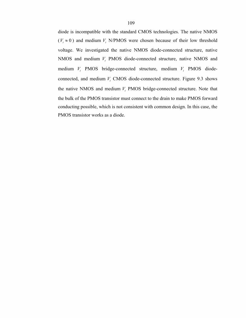
109
diode is incompatible with the standard CMOS technologies. The native NMOS
( 0tV ≈ ) and medium tV N/PMOS were chosen because of their low threshold
voltage. We investigated the native NMOS diode-connected structure, native
NMOS and medium tV PMOS diode-connected structure, native NMOS and
medium tV PMOS bridge-connected structure, medium tV PMOS diode-
connected, and medium tV CMOS diode-connected structure. Figure 9.3 shows
the native NMOS and medium tV PMOS bridge-connected structure. Note that
the bulk of the PMOS transistor must connect to the drain to make PMOS forward
conducting possible, which is not consistent with common design. In this case, the
PMOS transistor works as a diode.
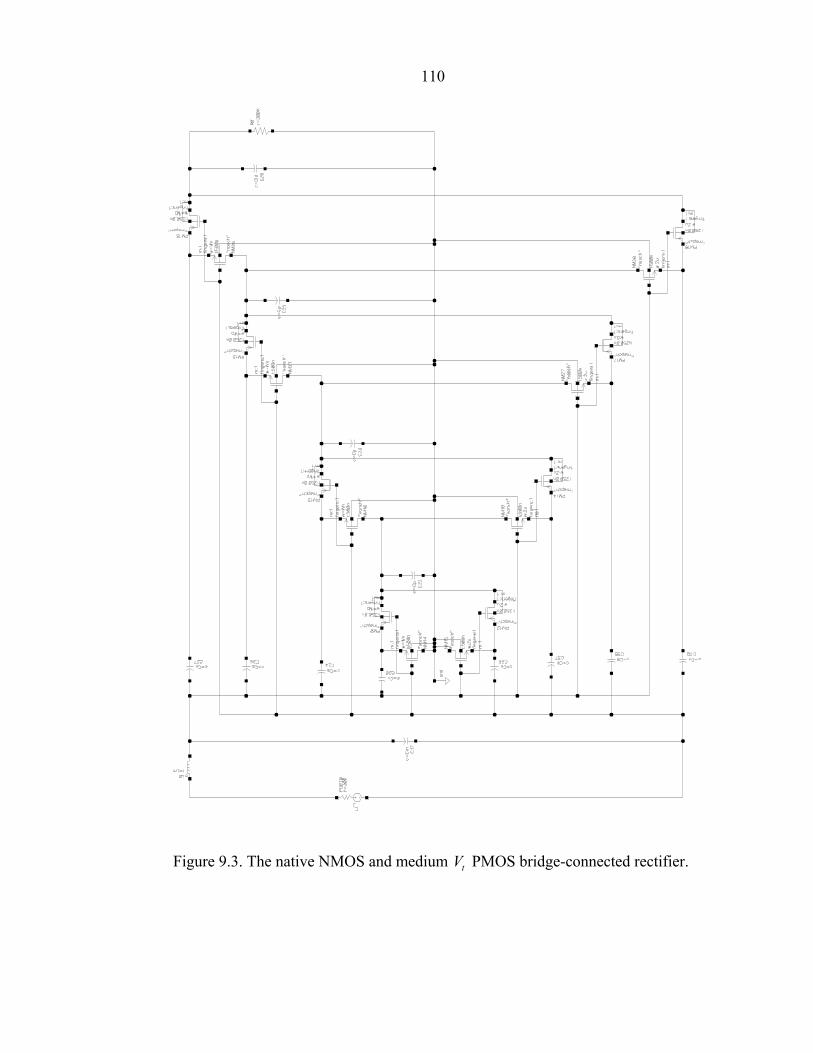
110
Figure 9.3. The native NMOS and medium tV PMOS bridge-connected rectifier.

111
Transistor size and stage number. The two factors of energy conversion loss are
resistive loss and rectifier leakage. The V-I property of a NMOS transistor in
active region can be expressed as
2( )2
oxd gs th
C WI V VL
μ= − (9.2)
where dI is the drain current; oxC is the oxide capacitance; μ is the permittivity;
W and L are the transistor width and length, respectively; and gsV is the gate-
source voltage. Equation (9.2) shows that a transistor with large WL
ratio has a
small insertion loss. However, a larger transistor results in larger parasitic
capacitance, i.e., higher leakage. From an RF viewpoint, all transistors in the
staged rectifier are in parallel connection, resulting in a large forward-biased
transistor and a large reverse-biased transistor. Therefore, the stage number and
transistor size have similar effects on the output power outV . Selecting a suitable
stage number and transistor size depends on the load, rectifier structure, and
transistor type.
Storage capacitor size. The circuit’s serial and shunt capacitors (Figure 7.5 and
Figure 7.6) are used to store charge. A small capacitor may result in low outV , but
a big capacitor may introduce a long charging time. Determination of capacitor
size is based on the charging and discharging time constant, which is usually
estimated by experience and proven by simulations. The preliminary selection of
the capacitor could be given by the following equations
( )1 1s p
ld d
C CfR fR n
< < , and ldld
TCR
> (9.3)
where sC and pC is the serially and parallel connected capacitor to the rectifier
circuit, respectively; dR is the equivalent resistance of the diode/MOSFET; n is
the number of rectifier stages; ldC is the capacitance of the final stage; ldR is the
equivalent resistive load of the IC, excluding the rectifier circuit; T is the desired
working time interval; and f is the working frequency.

112
Effective resistive load. The resistive load also affects rectifier design. It is
observed that the current consumption of the digital IC varies in different
operating conditions, i.e., the equivalent resistive load varies. It is difficult to
accurately estimate an equivalent resistive load of the digital IC. However, the
worst case (maximum current) is usually selected for the design.
An efficient rectifier must compromise with these parameters to reach the maximum
power delivery.
9.2.4 Voltage regulator
The voltage regulator specifies the input voltage range, i.e., the minimal and the
maximal acceptable voltage for the digital circuit. Figure 7.9 shows that the input power
of the tag can vary more than 20 dB. High input power may burn the IC, resulting in
possible permanent damage. Small input power may be unable to completely turn on the
IC, which will then malfunction. This variation must be adjusted by the circuit. One
challenge for the regulator design is its low-power requirement.
Figure 9.4 shows the schematics of a power regulator. It consists of two parts: the
reset circuit block for low power and the shunt circuit block for high power. Both blocks
are self-biased via diode-connected transistors (which work as the voltage divider). The
reset circuit block will turn off the power supply when the input voltage is lower than the
minimum, and turn it on when the input voltage meets the minimum requirement. All
operations are realized by switching on/off PMOS 0M . The inverter A is used as the
voltage level detector. When the input voltage increases to a certain level, the output of
the inverter A is reversed. The following two inverters are used to amplify the control
signal of 0M to achieve the rail-rail swing. The shunt circuit block operates similarly.
When the input voltage reaches the maximum, the inverter B reverses its output and the
shunt PMOS 1M is turned on. Extra current flows through 1M , resulting in a large
voltage drop across the rectifier and the power source. Thus, a reasonable output voltage
level is maintained for the digital circuit block even at high input power. The
combination of these two blocks provides a stable voltage regulation. However, this
regulator is passive, variation of threshold voltage and temperature could change the
voltage range.
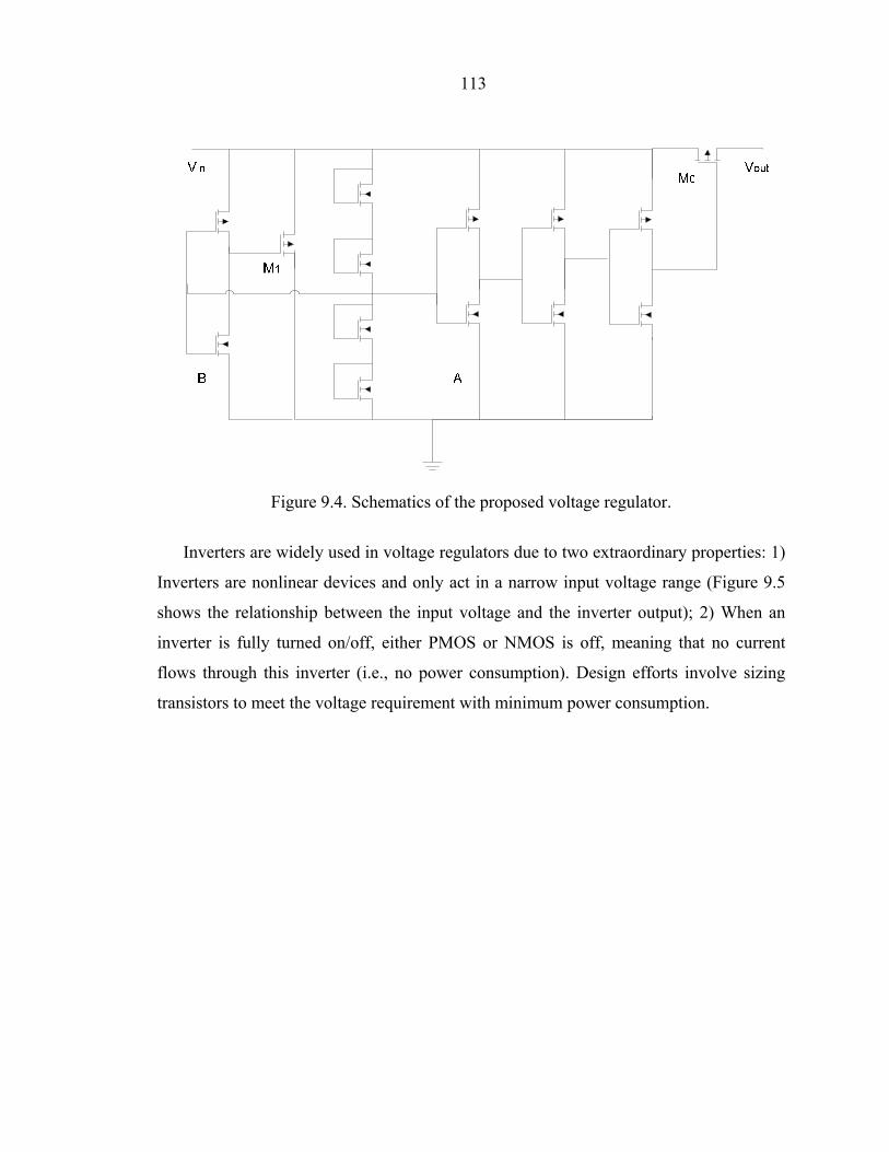
113
Figure 9.4. Schematics of the proposed voltage regulator.
Inverters are widely used in voltage regulators due to two extraordinary properties: 1)
Inverters are nonlinear devices and only act in a narrow input voltage range (Figure 9.5
shows the relationship between the input voltage and the inverter output); 2) When an
inverter is fully turned on/off, either PMOS or NMOS is off, meaning that no current
flows through this inverter (i.e., no power consumption). Design efforts involve sizing
transistors to meet the voltage requirement with minimum power consumption.
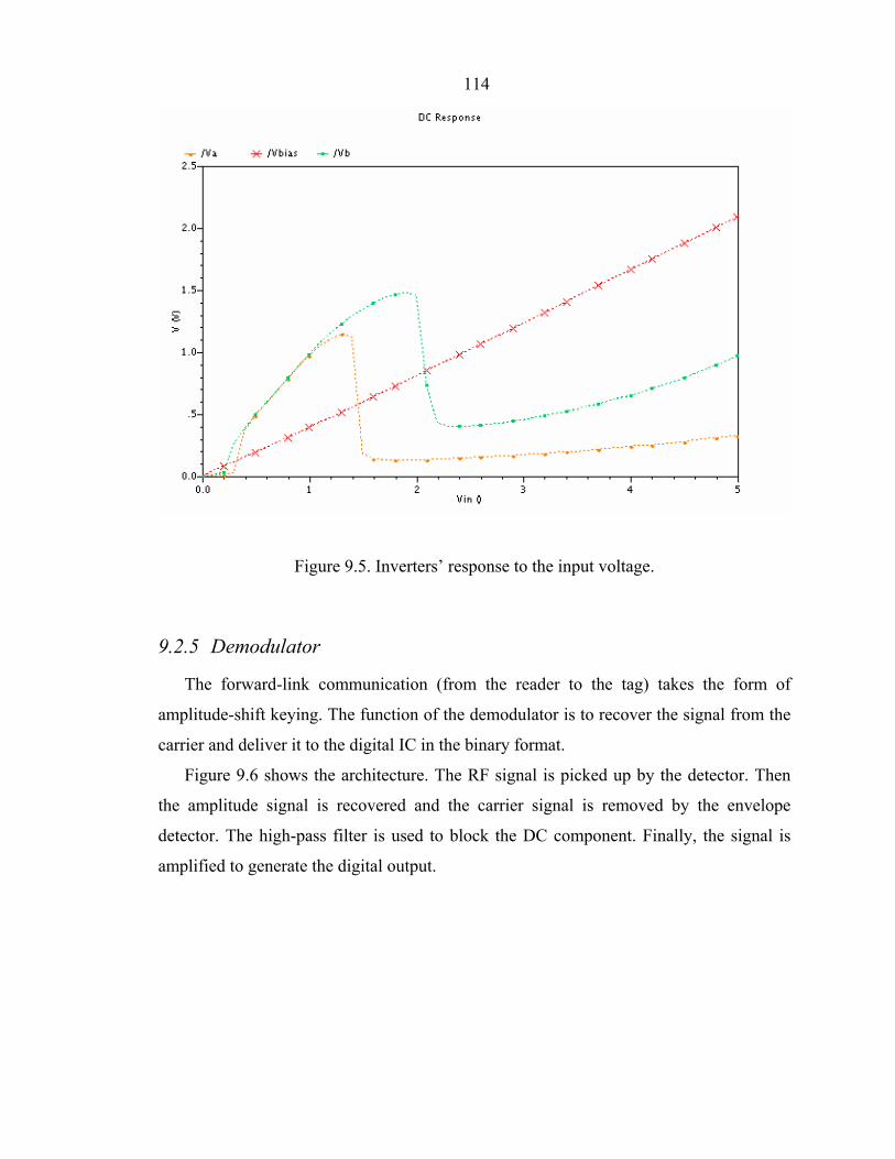
114
Figure 9.5. Inverters’ response to the input voltage.
9.2.5 Demodulator
The forward-link communication (from the reader to the tag) takes the form of
amplitude-shift keying. The function of the demodulator is to recover the signal from the
carrier and deliver it to the digital IC in the binary format.
Figure 9.6 shows the architecture. The RF signal is picked up by the detector. Then
the amplitude signal is recovered and the carrier signal is removed by the envelope
detector. The high-pass filter is used to block the DC component. Finally, the signal is
amplified to generate the digital output.
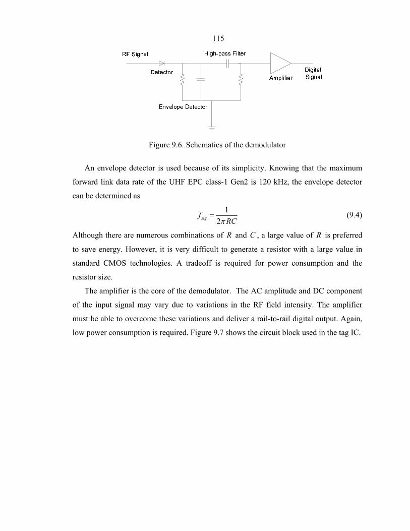
115
Figure 9.6. Schematics of the demodulator
An envelope detector is used because of its simplicity. Knowing that the maximum
forward link data rate of the UHF EPC class-1 Gen2 is 120 kHz, the envelope detector
can be determined as
12sigf
RCπ= (9.4)
Although there are numerous combinations of R and C , a large value of R is preferred
to save energy. However, it is very difficult to generate a resistor with a large value in
standard CMOS technologies. A tradeoff is required for power consumption and the
resistor size.
The amplifier is the core of the demodulator. The AC amplitude and DC component
of the input signal may vary due to variations in the RF field intensity. The amplifier
must be able to overcome these variations and deliver a rail-to-rail digital output. Again,
low power consumption is required. Figure 9.7 shows the circuit block used in the tag IC.

116
Figure 9.7. Amplifier circuit used in the demodulator
9.2.6 Uplink modulator
The uplink modulator is another key component. It transmits tag information to the
reader by using backscatter technology. When the tag IC’s impedance changes by
shorting the tag antenna, a mismatch occurs between the tag antenna and the tag IC, and
some of the incoming energy is reflected back to the reader. The reader can identify the
tag ID by detecting this reflected signal. The more energy is reflected, the higher the
signal-to-noise ratio is. Thus, a more reliable link is established between the reader and
the tag. The reflection factor Γ is expressed as
IC ANT
IC ANT
Z ZZ Z
−Γ =
+ (9.5)
where, ICZ is the impedance of the tag IC, which includes the matching network, and
ANTZ is the antenna impedance. According to (9.5), 0ICZ = or ICZ = ∞ can result in
the maximum reflection. However, only 0ICZ = is simple enough to be feasible. Figure
9.8 shows its implementation. The NMOS transistor sM (Figure 9.8) must be well sized.
It should be able to short the antenna effectively, and have small leakage during normal
operation. Figure 9.9 shows the performance of the proposed backscatter, which
demonstrates 70% reflection.
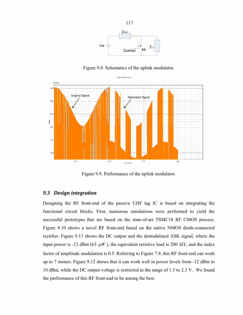
117
Figure 9.8. Schematics of the uplink modulator.
Original Signal Modulated Signal
Figure 9.9. Performance of the uplink modulator.
9.3 Design integration
Designing the RF front-end of the passive UHF tag IC is based on integrating the
functional circuit blocks. First, numerous simulations were performed to yield the
successful prototypes that are based on the state-of-art TSMC18 RF CMOS process.
Figure 9.10 shows a novel RF front-end based on the native NMOS diode-connected
rectifier. Figure 9.11 shows the DC output and the demodulated ASK signal, where the
input power is -12 dBm (63 Wμ ), the equivalent resistive load is 200 kΩ , and the index
factor of amplitude modulation is 0.5. Referring to Figure 7.9, this RF front-end can work
up to 7 meters. Figure 9.12 shows that it can work well in power levels from -12 dBm to
10 dBm, while the DC output voltage is restricted in the range of 1.5 to 2.3 V. We found
the performance of this RF front-end to be among the best.
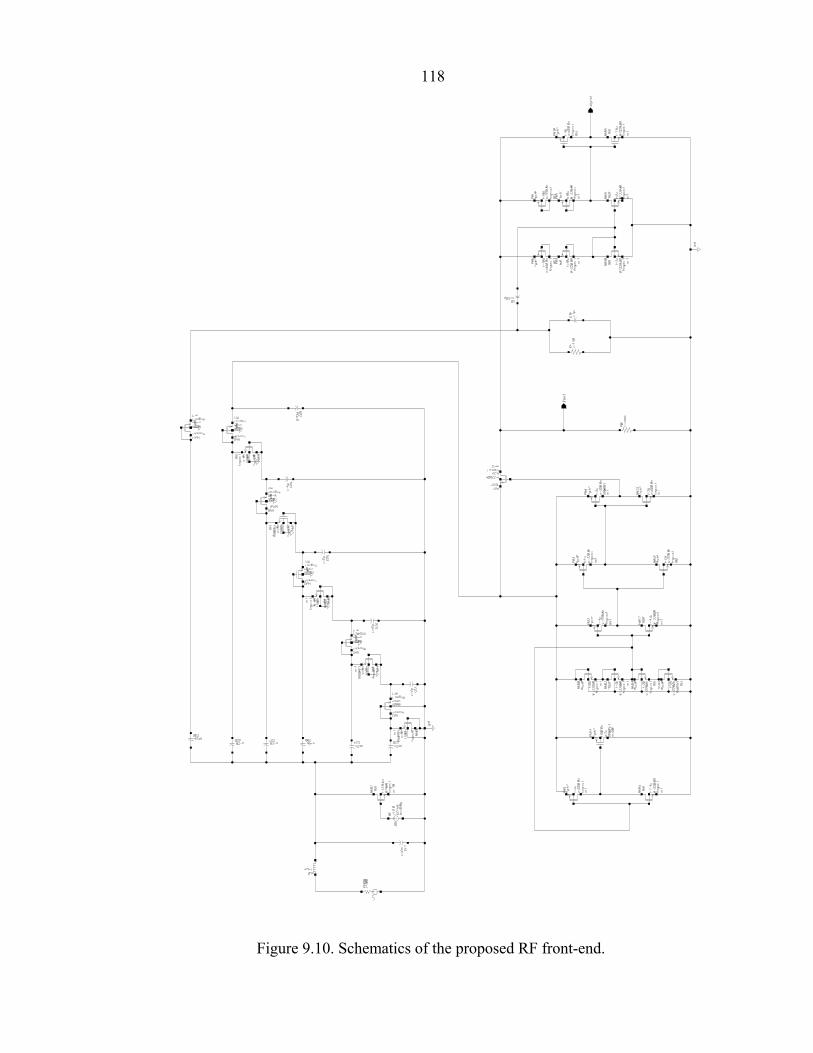
118
Figure 9.10. Schematics of the proposed RF front-end.

119
Figure 9.11. Simulation result of the proposed RF front-end (input power = -12 dBm, load = 200 kΩ , and AM index factor = 0.5).
Figure 9.12. Simulation result of the proposed RF front-end (load = 200 kΩ , and AM index factor = 0.5).
120
9.4 Conclusions
The RF front-end of the passive UHF RFID tag IC is successfully designed based on the
TSMC®18 fabrication technology. It includes four functional parts: a matching network
for maximum power delivery, a rectifier for high power conversion efficiency, a voltage
regulator for the power-on reset and over-voltage protection, a demodulator for digital
signal recovery, and an uplink modulator for data transmitting. The rectifier structure is
based on the native NMOS diode-connected structure. Simulations showed that this novel
IC can drive an equivalent 200 kΩ load at 1.6 V with -12 dBm input power, resist large
input power variations, and provide a demodulated rail-to-rail digital output signal. This
design meets the low-cost and low-power (long-range) requirements of RFID
applications.

121
Chapter 10. Future Research and Conclusions
10.1 Current problems
We identified the following problems that should be resolved in the near future.
Mechanical stability
When traveling along a cable, the robot must remain on the top. The current robot has
longitudinal and azimuthal degrees of freedom with respect to the cable. There must be
no less than two independent inputs to keep the robot under control. Our current design
only has one control variable input along the cable, and cannot guarantee stability.
Control strategies
As a multi-body dynamic system, the robot should have robust control stability. It
should be able to correct itself after a tilt, stay on top of the cable when it negotiates
obstacles, and avoid collisions. Optimum algorithms should be used to position the sensor
array with respect to the inspected system, path planning algorithm used to track the
entire (or portion) network with the shortest path, and control sequences adaptively by
switching sensor inspections between fast and slow modes. A smaller driving force will
result in an imperfect connection between the sensor and the cable surface, and a larger
force may damage the sensor. Therefore, it appears reasonable to use force feedback
control on the sensor actuator.
Power supply
Since the cable network is a global distributed system, it is impossible for an
inspecting robot to trail a power cord behind itself. Ideally, the power supply should be
wireless. It is desirable that the platform harvests energy from energized cables, possibly
122
by using inductive coupling for the wireless power supply. Although a low frequency
coupling is less efficient than a microwave mode, direct proximity to the power cable
makes it a viable choice. Inductive coupling is limited by metal-shielded cables. The
platform requires an independent backup power source.
Experiment problems
The relationship between external phenomena and the aging status of cable systems
can only be formulated based on a large number of experiments. The process is limited
because the experiments are time-consuming, and real PD samples – especially the
different types of PD -- are difficult to obtain.
Signal processing
Processing collected data is the most important step for identifying insulation status.
There are still no signal-processing methods available to integrate signals especially
when several sensors are used simultaneously for the measurement of insulation
properties. Signal processing should include algorithms to identify failure types, locate
the 3D position of the PD source, recognize the size and shape of voids, formulate the
relationship between the dielectrometry constants and aging status, and determine the
current status of insulation materials.
Passive RFID-enhanced sensing node
The passive RFID-enhanced sensor network is preferred for ubiquitous monitoring
because of its low cost, longevity, and wireless communication. However, its use is
limited by two factors. First, to effectively increase working range, the tag IC and the
sensor must be energy efficient and the power management strategies must be
implemented in the chip to decrease the idle cycles. Second, there is a scarcity of sensing
nodes, such as nodes with temperature, motion (acceleration), moisture, or light sensing
functions. The fabrication of the acceleration sensor, for example, is incompatible with
existing CMOS technology. The CMOS-based sensors are desirable due to its low cost.
Data transfer is an additional obstacle. EPC and ISO standards have been adopted
worldwide as RFID protocols. However, these existing protocols can only transfer the
tag’s ID information. New protocols are needed for compatibility.

123
10.2 Future work
The following sub-projects are now being refined, modified and executed, or are in the
planning stage;
Robotic platform
Improving the steering system to keep the robot on top of the cable; designing a
sensor actuator to drive an acoustic emission sensor and a fringing electrical field sensor.
Robust control
Developing a robust control algorithm that can realize the dynamic control of the
robot based on the closed-loop feedback (the feedback signals are longitude velocity and
vertical acceleration signals measured by encoders and accelerometers).
PD experiments
Simulating different types of PD to develop an efficient algorithm for identification
by changing positions of the AE sensor; changing sizes of voids; and changing shapes of
voids.
Insulation status experiments
Designing an FEF sensor with suitable patterns to achieve optimum sensitivity and
information about insulation materials; formulating the relationship between the
dielectrometry properties and the aging status of insulation materials; use the accelerated
aging experiment method to generate suitable samples (to overcome the shortfall of real
samples).
New passive RFID-enhanced sensor node design
RFID-enhanced sensors, such as temperature sensing and motion sensing, are under
development; to interface with sensors, it is necessary to introduce supporting circuits in
the chip, including amplifiers and ADC. Low power consumption is the design criterium.
The CMOS-based temperature sensor can be easily integrated into the tag IC.
However, it is difficult to design a good voltage/current reference on the chip due to the
energy budget. Overcome the restrictions of the resolution and dynamic range of
measurement. MEMS sensors, such as accelerometers, are incompatible with the CMOS
fabrication process. However, motion can be indirectly detected by measuring the signal
intensity, which usually varies in different locations. Thus, a mocked motion sensor can
be implemented via CMOS technologies.

124
10.3 Conclusions
This dissertation develops a prototype monitoring robot that can identify the aging status
and locate incipient failures of power cable systems. We accomplished the following:
1) Based on the derived cost-driven model, our hybrid maintenance method almost
reaches minimum operational cost by combining the advantages of traditional
strategies. Our results showed that mobile monitoring can be a solution for future
maintenance strategies.
2) The mobile robot functioned as a mobile platform for underground cable systems.
The platform is modular and utilizes mechanical appendages to achieve
operational stability. Equipping the control board with four distributed micro-
controllers greatly increased the robot’s performance. A modified serial peripheral
interface bus and corresponding protocol were developed for the communication
between the master and slave micro-controllers. Sets of software were developed
to implement the Internet control for the robot.
3) A DSP-based data acquisition system consisting of a TI C6711DSK, a
THS1408EVM ADC board, an over-voltage protector, and sensors was designed.
Enhanced direct memory access and threshold-value detection were implemented
to “free up” the CPU resources. An over-voltage protector based on an optical
coupler was added to prevent possible damage to the ADC board.
4) Operational principles and experimental setups for the infrared sensor, the
acoustic sensor, and the fringing electric field sensor were introduced and
preliminary experimental results obtained.
5) Antenna design methods for HF RFID and corresponding design parameters were
presented in detail. Based on the proposed methods, induced voltage on the RFID
tag can be attained. Adaptive matching algorithms were suggested for the
maximum energy delivery to improve system performance.
6) The RF front-end IC of passive UHF tag was designed based on TSMC18
technology. It included a matching network for the maximum power delivery, a
rectifier for the high power conversion efficiency, a voltage regulator for the
power on reset and over-voltage protection, and a demodulator for digital signal
recovery. Simulations revealed that this novel design can drive an equivalent 200

125
kΩ load at 1.6 V with -12 dBm input power and resist the large input power
variation.
We conclude that mobile monitoring is a viable solution for the maintenance of
underground electric cable systems. This project displays the usefulness of a mobile
robotic platform for robotic inspection and monitoring of over head lines, nuclear plants,
and underwater cables.
126
END NOTES
[1] "The need for a balanced national energy policy," National Energy Policy Council (NEPC). 2004. Association of Energy Engineers.
[2] H. Ng, "Cutting the time it takes to locate underground distribution faults," The Distribution News, [4]. 1997. Electrical Power Research Institute, Inc.
[3] CEIDS (Consortium for Electric Infrastructure to Support a Digital Society), "The Cost of Power Disturbances to Industrial and Digital Economy Companies Executive Summary," 2001.
[4] W. Reder and D. Flaten, "Reliability Centered Maintenance for Distribution Underground Systems," IEEE Power Engineering Society Summer Meeting, vol. 1, 2000, pp. 551-556.
[5] M. Gaynor, S. L. Moulton, M. Welsh, E. LaCombe, A. Rowan, and J. Wynne, "Integrating Wireless Sensor Networks With the Grid," IEEE Internet Computing, vol. 8, no. 4, pp. 32-39, July 2004.
[6] K. Martinez, J. K. Hart, and R. Ong, "Sensor Network Applications," Computer, vol. 37, no. 8, pp. 50-56, Aug. 2004.
[7] C. Y. Chong and S. P. Kumar, "Sensor Networks: Evolution, Opportunities, and Challenges," Proceedings of the IEEE, vol. 91, no. 8, pp. 1247-1256, Aug. 2003.
[8] B. Jiang, K. P. Fishkin, S. Roy, and P. Matthai, "Unobtrusive Long-Range Detection of Passive RFID Tag Motion," IEEE Transactions on Instrumentation and Measurement, 2005.
[9] K. P. Fishkin, B. Jiang, M. Philipose, and S. Roy, "I Sense a Disturbance in the Force: Unobtrusive Detection of Interactions With RFID-Tagged Objects," Ubicomp 2004: Ubiquitous Computing, Proceedings, vol. 3205, pp. 268-282, 2004.
[10] M. Tsutsui, H. Tsuchihashi, K. Satoh, M. Mukaida, H. Watanabe, S. Mori, Y. Kojima, and S. Yokoyama, "Manipulator System for Constructing Overhead Distribution Lines," IEEE Transactions on Power Delivery, vol. 4, no. 2, pp. 1904-1909, July 1989.
[11] S. Nio and Y. Maruyama, "Remote-Operated Robotic System for Live-Line Maintenance Work," ESMO-93 Sixth International Conference on Transmission and Distribution Construction and Live Line Maintenance, 1993, pp. 425-435.
[12] M. Nakashima, H. Yakabe, Y. Maruyama, K. Yano, K. Morita, and H. Nakagaki, "Application of Semi-Automatic Robot Technology on Hot-Line Maintenance Work," IEEE International Conference on Robotics and Automation, vol. 1, 1995, pp. 843-850.

127
[13] M. Boyer, "Systems Integration in Telerobotics: Case Study: Maintenance of Electric Power Lines," 1996 IEEE International Conference on Robotics and Automation, 1996, pp. 1042-1047.
[14] A. Santamaria, R. Aracil, A. Tuduri, P. Martinez, F. Val, L. F. Penin, M. Ferre, E. Pinto, and A. Barrientos, "Teleoperated Robots for Live Power Lines Maintenance (ROBTET)," 14th International Conference and Exhibition on Electricity Distribution, vol. 3, 1997, pp. 31-1-31/5.
[15] J. Sawada, K. Kusumoto, Y. Maikawa, T. Munakata, and Y. Ishikawa, "A Mobile Robot For Inspection of Power Transmission Lines," IEEE Transactions on Power Delivery, vol. 6, pp. 309-315, 1991.
[16] H. Kobayashi, H. Nakamura, and T. Shimada, "An Inspection Robot For Feeder Cables-Basic Structure And Control," International Conference on Industrial Electronics, Control and Instrumentation, vol. 2, 1991, pp. 992-995.
[17] EPRI, "Assessment of Robotics for Boiler NDE and Repair," 2000.
[18] N.Ishikawa and K.Suzuki, "Development of a Human and Robot Collaborative System for Inspecting Patrol of Nuclear Power Plants," Proceedings of the 6th IEEE International Workshop on Robot and Human Communication, 1997, pp. 118-123.
[19] Seungho Kim, Seung Ho Jung, and Chang Hoi Kim, "Preventive Maintenance and Remote Inspection of Nuclear Power Plants Using Tele-Robotics," Proceedings of IEEE/RSJ International Conference on Intelligent Robots and Systems, vol. 1, 1999, pp. 603-608.
[20] E. M. Petriu, T. E. Whalen, R. Abielmona, and A. Stewart, "Robotic Sensor Agents: a New Generation of Intelligent Agents for Complex Environment Monitoring," IEEE Instrumentation and Measurement Magazine, vol. 7, no. 3, pp. 46-51, 2004.
[21] A. Zagler and F. Pfeiffer, ""MORITZ" a Pipe Crawler for Tube Junctions," Proceedings of IEEE International Conference on Robotics and Automation, vol. 3, 2003, pp. 2954-2959.
[22] S. G. Roh, S. M. Ryew, J. H. Yang, and H. R. Choi, "Actively Steerable in-Pipe Inspection Robots for Underground Urban Gas Pipelines," Proceedings 2001 ICRA IEEE International Conference on Robotics and Automation, vol. 1, 2001, pp. 761-766.
[23] H. T. Roman, B. A. Pellegrino, and W. R. Sigrist, "Pipe Crawling Inspection Robots: an Overview," IEEE Transactions on Energy Conversion, vol. 8, no. 3, pp. 576-583, 1993.
[24] J. Weston, "A Safer Way to Search Disaster Sites," IEEE Robotics & Automation Magazine, vol. 7, no. 3, pp. 56-57, 2004.
[25] A. M. Bertetto and M. Ruggiu, "In-Pipe Inch-Worm Pneumatic Flexible Robot," Proceedings of 2001 IEEE/ASME International Conference on Advanced Intelligent Mechatronics, vol. 2, 2001, pp. 1226-1231.

128
[26] J. A. Galvez, P. Gonzalez de Santos, and F. Pfeiffer, "Intrinsic Tactile Sensing for the Optimization of Force Distribution in a Pipe Crawling Robot," IEEE/ASME Transactions on Mechatronics, vol. 6, no. 1, pp. 26-35, 2001.
[27] S. Guo, Y. Sasaki, and T. Fukuda, "A New Kind of Microrobot in Pipe Using Driving Fin," Proceedings of 2003 IEEE/ASME International Conference on Advanced Intelligent Mechatronics, vol. 2, 2003, pp. 697-702.
[28] S. A. Boggs, "Partial Discharge - Part I: Overview and Signal Generation," IEEE Electrical Insulation Magazine, vol. 6, no. 4, pp. 33-39, 1990.
[29] Oyegoke, B., Hyvonen, P., and Aro, M., "Partial discharge measurements as diagnostic tool for power cable systems," Helsinki University of Technology, 2001.
[30] R. Harrold, "Partial Discharge - Part XVI. Ultrasonic Sensing of PD Within Large Capacitors ," IEEE Electrical Insulation Magazine, vol. 9, no. 3, pp. 21-28, 1993.
[31] K. Fukunaga, M. Tan, and H. Takehana, "New Partial Discharge Detection Method for Live Uhv Ehv Cable Joints," IEEE Transactions on Electrical Insulation, vol. 27, no. 3, pp. 669-674, June 1992.
[32] E. Watanabe, T. Moriya, and M. Yoshizawa, "Ultrasonic Visualization Method of Electrical Trees Formed in Organic Insulating Materials," IEEE Transactions on Dielectrics and Electrical Insulation, vol. 5, no. 5, pp. 767-773, 1998.
[33] F. Weigand, H. W. Spiess, K. Moller, B. Blumich, and G. Salge, "Nuclear Magnetic Resonance Imaging of Electrical Trees in PE," IEEE Transactions on Dielectrics and Electrical Insulation, vol. 4, no. 3, pp. 280-285, 1997.
[34] N. Grassie and G. Scott, Polymer Deregulation and Stabilisation, Cambridge University Press, 1929.
[35] J. Densley, "Ageing Mechanisms and Diagnostics for Power Cables - An Overview," IEEE Electrical Insulation Magazine, vol. 17, no. 1, pp. 1820-1824, Jan. 2001.
[36] G. Lichtenberg, "Novi Commentarii Societatis Regiae Gottingae tom 8," [168]. 1777.
[37] J. C. Maxwell, A Treatiese on Electricity and Magnetism, Clarendon Press, Oxford, 1873.
[38] Oyegoke, B., P.Hyvonen, and Aro, M., "Partial Discharge Measurement as Diagnostic Tool for Power Cable Systems," Helsinki University of Technology, 2001.
[39] Y. Nakanishi and et al, "Development of a Live-Line Partial Discharge Detection Method for XLPE Insulated Copper Wire-Shielded Cable Using a Yoke Coil," Electrical Engineering in Japan, vol. 113, no. 8, pp. 59-72, 1993.
129
[40] P. Wouters and et al, "Inductive Ultral-Wide Band Detection and Location of Partial Discharges in High Voltage Cables," European Transactions on Electrical Power, vol. 4, no. 3, pp. 223-229, 1994.
[41] G. Katsuta, A. Toya, K. Muraoka, T. Endoh, Y. Sekii, and C. Ikeda, "Development of A Method of Partial Discharge Detection in Extra-High-Voltage Cross-Linked Polyethylene Insulated Cable Lines," IEEE Transactions on Power Delivery, vol. 7, no. 3, pp. 1068-1079, July 1992.
[42] D. Pommerenke, T. Strehl, and W. Kalkner, "Directional Coupler Sensor for Partial Discharge Recognition on High Voltage Cable Systems," 10th International Symposium on High Voltage, 1997.
[43] E. Lemke, T. Strehl, and D. Russwurm, "New Development in the Field of PD Detection and Location in Power Cable Under On-Site Condition," Eleventh International Symposium on High Voltage Engineering, vol. 5, 1999, pp. 106-111.
[44] L. E. Lundgaard, "Partial Discharge - Part XIV. Acoustic Partial Discharge Detection-Practical Application," IEEE Electrical Insulation Magazine, vol. 8, no. 5, pp. 34-43, 1992.
[45] L. E. Lundgaard, "Partial Discharge - Part XIII. Acoustic Partial Discharge Detection-Fundamental Consideration," IEEE Electrical Insulation Magazine, vol. 8, no. 4, pp. 25-31, 1992.
[46] Y. Tian, P. L. Levin, A. E. Davies, and G. Hathaway, "Acoustic Emission Techniques for Partial Discharge Detection Within Cable Insulation," IEE Eighth International Conference on Dielectric Materials, Measurements and Applications, 2000, pp. 503-508.
[47] A. Zargari and T. R. Blackbum, "Modified Optical Fibre Sensor for PD Detection in High Voltage Power Equipment," IEEE International Symposium on Electrical Insulation, vol. 1, 1996, pp. 424-427.
[48] Z. Q. Zhao, M. MacAlpine, and M. S. Demokan, "The Directionality of an Optical Fiber High-Frequency Acoustic Sensor for Partial Discharge Detection and Location," Journal of Lightwave Technology, vol. 18, no. 6, pp. 795-806, June 2000.
[49] I. J. Kemp, "Partial Discharge Plant-Monitoring Technology - Present and Future-Developments," IEE Proceedings-Science, Measurement and Technology, vol. 142, no. 1, pp. 4-10, Jan. 1995.
[50] H. Yamashita, "Partial Discharge Measurements in Dielectric Liquids Under Impulse Voltage," IEEE Transactions on Electrical Insulation, vol. 28, no. 6, pp. 947-955, Dec. 1993.
[51] D. Pommerenke and K. Masterson, "A Novel Concept for Monitoring Partial Discharge on EHV-Cable System Accessories Using No Active Components at the Accessories," Eighth International Conference on Dielectric Materials, Measurements and Application (IEE Conf. Publ. No. 473), 2000, pp. 145-149.
130
[52] J. M. Braun and F. Y. Chu, "Novel Low-Cost SF//6 Arching Byproduct Detectors for Field Use in Gas-Insulated Switchgear," IEEE Transactions on Power Delivery, vol. PWRD-1, no. 2, pp. 81-86, 1986.
[53] M. Duval, "Dissolved Gas Analysis: It Can Save Your Transformer," IEEE Electrical Insulation Magazine, vol. 8, no. 6, pp. 22-27, 1989.
[54] J. Unsworth and F. Mitchell, "Degradation of Electrical Insulating Paper Monitored With High-Performance Liquid-Chromatography," IEEE Transactions on Electrical Insulation, vol. 25, no. 4, pp. 737-746, Aug. 1990.
[55] T. Sasake, M. Kurihara, M. Uchida, T. Nakamura, and H. Kawakami, "Oil-Filled Cable Surveillance System Using Newly Developed Optical Fiber Gas Sensor ," IEEE Transactions on Power Delivery, vol. 11, no. 2, pp. 656-662, 1996.
[56] N. H. Ahmed and N. Srinivas, "On-Line Partial Discharge Measuring Technique in High-Pressure Gas-Filled Terminations," Annual Report on Electrical Insulation and Dielectric Phenomena, vol. 2, 1998, pp. 386-389.
[57] N. J. Goldfine, A. P. Washabaugh, J. V. Dearlove, and P. A. von Guggenberg, "Imposed Omega-k Magnetometer and Dielectrometer Applications," Review of Progress in Quantitative Nondestructive Evaluation, vol. 12, New York, 1993.
[58] Y. K. Sheiretov and M. Zahn, "Dielectrometry Measurements of Moisture Dynamics in Oil-Impregnated Pressboard," IEEE Transactions on Dielectrics and Electrical Insulation, vol. 2, no. 3, pp. 329-351, June 1995.
[59] M. C. Zaretsky, P. Li, and J. R. Melcher, "Estimation Of Thickness, Complex Bulk Permittivity And Surface Conductivity Using Interdigital Dielectrometry," IEEE Transactions on Electrical Insulation, vol. 24, no. 6, pp. 1159-1166, Dec. 1989.
[60] J. O. Simpson and S. A. Bidstrup, "Modeling Conductivity and Viscosity Changes During Epoxy Cure Using TEA DMA and DSC," Proceedings of the American Chemical Society Division of Polymeric Materials: Science and Engineering Fall Meeting, vol. 69, no. 3, pp. 451-452, 1993.
[61] I. G. Matis, "On Multiparameter Control Of Dielectric Properties Of Laminate Polymer Materials," Latvijas PSR Zinatnu Akademijas Vestis Fizikas un Tehnisko, no. 6, pp. 60-67, 1966.
[62] S. D. Senturia and C. M. Sechen, "The Use of the Charge-Flow Transistor to Distinguish Surface and Bulk Components of Thin-Film Sheet Resistance," IEEE Transactions on Electron Devices, vol. ED-24, no. 9, pp. 1207, Sept. 1977.
[63] R. S. Jachowicz and S. D. Senturia, "A Thin-Film Capacitance Humidity Sensor," Sensors and Actuators, vol. 2, no. 2, pp. 171-186, Dec. 1981.
[64] A. V. Mamishev, Y. Du, B. C. Lesieutre, and M. Zahn, "Development and Applications of Fringing Electric Field Sensors and Parameter Estimation Algorithms," Journal of Electrostatics, vol. 46, pp. 109-123, 1999.

131
[65] J. Densley, "Ageing Mechanisms and Diagnostics for Power Cables - An Overview," IEEE Electrical Insulation Magazine, vol. 17, no. 1, pp. 1820-1824, Jan. 2001.
[66] H. Stochman, "Communication by Means of Reflected Power," Proceedings of IEE, pp. 1196-1204, 1948.
[67] J. Landt, "Shrouds of Time – the History of RFID," RFID Connections, no. 2, 2002.
[68] V. Stanford, "Pervasive Computing Goes the Last Hundred Feet With RFID Systems," IEEE Pervasive Computing, vol. 2, no. 2, pp. 9-14, 2003.
[69] K. Finkenzeller, RFID handbook: fundamentals and applications in contactless smart cards and identification, 2 ed., Wiley, 2003.
[70] E. H. Callaway, Wireless sensor networks: architectures and protocols, CRC Press, 2004.
[71] Z.Zhu, B.Jamali, and P.H.Cole, "Brief comparison of different rectifier structures for HF and UHF RFID (Phase II)," Auto-ID Labs, 2004.
[72] Z.Zhu, B.Jamali, and P.H.Cole, "Brief comparison of different rectifier structures for HF and UHF RFID (Phase I)," Auto-ID Labs, 2004.
[73] J. R. Smith, B. Jiang, S. Roy, M. Philipose, K. Sundara-Rajan, and A. V. Mamishev, "ID Modulation: Embedding Sensor Data in an RFID Timeseries," Proceedings of the 7th Information Hiding Workshop, 2005.
[74] A. V. Mamishev, Y. Du, J. H. Bau, B. C. Lesieutre, and M. Zahn, "Evaluation of Diffusion-Driven Material Property Profiles Using Three-Wavelength Interdigital Sensor," IEEE Transactions on Dielectrics and Electrical Insulation, vol. 8, no. 5, pp. 785-798, Oct. 2001.
[75] R. Brammer, T. Bengtsson, T. Soqvist, B. Ullberg, J. Hedberg, I. Andersson, J. Sandstedt, and L. Dahlberg, "Acoustic PD Testing of Cable Joints in a Powerformer," Nordic Insulation Symposium, 2001.
[76] T. Boczar, "Identification of a Specific Type of PD From Acoustic Emission Frequency Spectra," IEEE Transactions on Dielectrics and Electrical Insulation, vol. 8, no. 4, pp. 598-606, 2001.
[77] Y. Tian, P. L. Lewin, A. E. Davies, S. J. Sutton, and S. G. Swingler, "Application of Acoustic Emission Techniques and Artificial Neural Networks to Partial Discharge Classification ," IEEE International Symposium on Electrical Insulation, 2002, pp. 119-123.
[78] M. M. A. Salama and R. Bartnikas, "Determination of Neural-Network Topology for Partial Discharge Pulse Pattern Recognition," IEEE Transactions on Neural Networks, vol. 13, no. 2, pp. 446-456, Mar. 2002.
[79] R. Bartnikas, "Partial Discharges-Their Mechanism, Detection, Measurement," IEEE Transactions on Dielectrics and Electrical Insulation, vol. 9, no. 5, pp. 763-808, Oct. 2002.
132
[80] M. M. A. Salama and R. Bartnikas, "Fuzzy Logic Applied to PD Pattern Classification," IEEE Transactions on Neural Networks, vol. 7, no. 1, pp. 118-123, 2000.
[81] L. Satish and W. S. Zaengl, "Can Fractal Features Be Used for Recognizing 3-D Partial Discharge Patterns," IEEE Transactions on Dielectrics and Electrical Insulation, vol. 2, no. 3, pp. 352-359, June 1995.
[82] P. von Glahn and R. J. Van Brunt, "Continuous Recording and Stochastic Analysis of PD ," IEEE Transactions on Dielectrics and Electrical Insulation, vol. 2, no. 4, pp. 590-601, 1995.
[83] E. Carminati, L. Cristaldi, M. Lazzaroni, and A. Monti, "Neuro-Fuzzy Approach for the Detection of Partial Discharge," IEEE Transactions on Instrumentation and Measurement, vol. 50, no. 5, pp. 1413-1417, Oct. 2001.
[84] A. Bolliger and E. Lemke, "PD Diagnostics - Its History and Future," PD Workshop, 2001.
[85] J. H. Williams, A. Davies, and P. R. Drake, Condition-based maintenance and machine diagnostics, Chapman & Hall, 1994.
[86] M. Philipose, J. R. Smith, B. Jiang, A. Mamishev, S. Roy, and K. Sundara-Rajan, "Battery-Free Wireless Identification and Sensing," IEEE Pervasive Computing, vol. 4, no. 1, pp. 37-45, Jan. 2005.
[87] J. Kraus, Antennas, 2 ed., McGraw-Hill, 1988.
[88] B. Jiang, J. R. Smith, M. Philipose, S. Roy, K. Sundara-Rajan, and A. V. Mamishev, "Energy Scavenging for Inductively Coupled Passive RFID Systems," IEEE Instrumentation and Measurement Technology Conference, vol. 2, 2005, pp. 984-989.
[89] C. Bowick, RF circuit design, Newnes, 1997.
[90] Z. Zhu, B. Jamali, and P. H. Cole, Brief comparison of different rectifier structures for HF and UHF RFID (Phase I), Auto-ID Labs, 2004.
[91] Z. Zhu, B. Jamali, and P. H. Cole, Brief comparison of different rectifier structures for HF and UHF RFID (Phase II), Auto-ID Labs, 2004.
[92] D. Pozar, Microwave engineering, 2 ed., John Wiley & Sons, 2003.
[93] "AN831: Matching small loop antennas to rfPIC devices," Microchip application notes. 2002.
[94] "Simple Inductance Formulas for Radio Coils," Proceedings of the IRE, vol. 16, no. 10, 1928.
[95] H. Greenhouse, "Design of Planar Rectangular Microelectronic Inductors," IEEE Transactions on Parts, Hybrids, and Packaging, vol. 10, no. 2, pp. 101-109, 1974.
[96] "AN680: microID 13.56 MHz RFID system design guide," Microchip application notes. 2001.

133
[97] B. Nauta and M. B. Dijkstra, "Analog Line Driver With Adaptive Impedance Matching," IEEE Journal of Solid-State Circuits, vol. 33, no. 12, pp. 1992-1998, 1998.
[98] M. Thompson and J. K. Fidler, "Application of the Genetic Algorithm and Simulated Annealing to LC Filter Tuning," IEE Proceedings G- Circuits, Devices and Systems, vol. 48, no. 4, pp. 177-182, 2001.
[99] Z. Zhu, RFID analog front end design tutorial (version 0.0), Auto-ID Labs, 2004.

134
REFERENCES
[1] "The need for a balanced national energy policy," National Energy Policy Council (NEPC). 2004. Association of Energy Engineers.
[2] H. Ng, "Cutting the time it takes to locate underground distribution faults," The Distribution News, [4]. 1997. Electrical Power Research Institute, Inc.
[3] CEIDS (Consortium for Electric Infrastructure to Support a Digital Society), "The Cost of Power Disturbances to Industrial and Digital Economy Companies Executive Summary," 2001.
[4] W. Reder and D. Flaten, "Reliability Centered Maintenance for Distribution Underground Systems," IEEE Power Engineering Society Summer Meeting, vol. 1, 2000, pp. 551-556.
[5] M. Gaynor, S. L. Moulton, M. Welsh, E. LaCombe, A. Rowan, and J. Wynne, "Integrating Wireless Sensor Networks With the Grid," IEEE Internet Computing, vol. 8, no. 4, pp. 32-39, July 2004.
[6] K. Martinez, J. K. Hart, and R. Ong, "Sensor Network Applications," Computer, vol. 37, no. 8, pp. 50-56, Aug. 2004.
[7] C. Y. Chong and S. P. Kumar, "Sensor Networks: Evolution, Opportunities, and Challenges," Proceedings of the IEEE, vol. 91, no. 8, pp. 1247-1256, Aug. 2003.
[8] B. Jiang, K. P. Fishkin, S. Roy, and P. Matthai, "Unobtrusive Long-Range Detection of Passive RFID Tag Motion," IEEE Transactions on Instrumentation and Measurement, 2005.
[9] K. P. Fishkin, B. Jiang, M. Philipose, and S. Roy, "I Sense a Disturbance in the Force: Unobtrusive Detection of Interactions With RFID-Tagged Objects," Ubicomp 2004: Ubiquitous Computing, Proceedings, vol. 3205, pp. 268-282, 2004.
[10] M. Tsutsui, H. Tsuchihashi, K. Satoh, M. Mukaida, H. Watanabe, S. Mori, Y. Kojima, and S. Yokoyama, "Manipulator System for Constructing Overhead Distribution Lines," IEEE Transactions on Power Delivery, vol. 4, no. 2, pp. 1904-1909, July 1989.
[11] S. Nio and Y. Maruyama, "Remote-Operated Robotic System for Live-Line Maintenance Work," ESMO-93 Sixth International Conference on Transmission and Distribution Construction and Live Line Maintenance, 1993, pp. 425-435.
[12] M. Nakashima, H. Yakabe, Y. Maruyama, K. Yano, K. Morita, and H. Nakagaki, "Application of Semi-Automatic Robot Technology on Hot-Line Maintenance Work," IEEE International Conference on Robotics and Automation, vol. 1, 1995, pp. 843-850.

135
[13] M. Boyer, "Systems Integration in Telerobotics: Case Study: Maintenance of Electric Power Lines," 1996 IEEE International Conference on Robotics and Automation, 1996, pp. 1042-1047.
[14] A. Santamaria, R. Aracil, A. Tuduri, P. Martinez, F. Val, L. F. Penin, M. Ferre, E. Pinto, and A. Barrientos, "Teleoperated Robots for Live Power Lines Maintenance (ROBTET)," 14th International Conference and Exhibition on Electricity Distribution, vol. 3, 1997, pp. 31-1-31/5.
[15] J. Sawada, K. Kusumoto, Y. Maikawa, T. Munakata, and Y. Ishikawa, "A Mobile Robot For Inspection of Power Transmission Lines," IEEE Transactions on Power Delivery, vol. 6, pp. 309-315, 1991.
[16] H. Kobayashi, H. Nakamura, and T. Shimada, "An Inspection Robot For Feeder Cables-Basic Structure And Control," International Conference on Industrial Electronics, Control and Instrumentation, vol. 2, 1991, pp. 992-995.
[17] EPRI, "Assessment of Robotics for Boiler NDE and Repair," 2000.
[18] N.Ishikawa and K.Suzuki, "Development of a Human and Robot Collaborative System for Inspecting Patrol of Nuclear Power Plants," Proceedings of the 6th IEEE International Workshop on Robot and Human Communication, 1997, pp. 118-123.
[19] Seungho Kim, Seung Ho Jung, and Chang Hoi Kim, "Preventive Maintenance and Remote Inspection of Nuclear Power Plants Using Tele-Robotics," Proceedings of IEEE/RSJ International Conference on Intelligent Robots and Systems, vol. 1, 1999, pp. 603-608.
[20] E. M. Petriu, T. E. Whalen, R. Abielmona, and A. Stewart, "Robotic Sensor Agents: a New Generation of Intelligent Agents for Complex Environment Monitoring," IEEE Instrumentation and Measurement Magazine, vol. 7, no. 3, pp. 46-51, 2004.
[21] A. Zagler and F. Pfeiffer, ""MORITZ" a Pipe Crawler for Tube Junctions," Proceedings of IEEE International Conference on Robotics and Automation, vol. 3, 2003, pp. 2954-2959.
[22] S. G. Roh, S. M. Ryew, J. H. Yang, and H. R. Choi, "Actively Steerable in-Pipe Inspection Robots for Underground Urban Gas Pipelines," Proceedings 2001 ICRA IEEE International Conference on Robotics and Automation, vol. 1, 2001, pp. 761-766.
[23] H. T. Roman, B. A. Pellegrino, and W. R. Sigrist, "Pipe Crawling Inspection Robots: an Overview," IEEE Transactions on Energy Conversion, vol. 8, no. 3, pp. 576-583, 1993.
[24] J. Weston, "A Safer Way to Search Disaster Sites," IEEE Robotics & Automation Magazine, vol. 7, no. 3, pp. 56-57, 2004.
[25] A. M. Bertetto and M. Ruggiu, "In-Pipe Inch-Worm Pneumatic Flexible Robot," Proceedings of 2001 IEEE/ASME International Conference on Advanced Intelligent Mechatronics, vol. 2, 2001, pp. 1226-1231.

136
[26] J. A. Galvez, P. Gonzalez de Santos, and F. Pfeiffer, "Intrinsic Tactile Sensing for the Optimization of Force Distribution in a Pipe Crawling Robot," IEEE/ASME Transactions on Mechatronics, vol. 6, no. 1, pp. 26-35, 2001.
[27] S. Guo, Y. Sasaki, and T. Fukuda, "A New Kind of Microrobot in Pipe Using Driving Fin," Proceedings of 2003 IEEE/ASME International Conference on Advanced Intelligent Mechatronics, vol. 2, 2003, pp. 697-702.
[28] S. A. Boggs, "Partial Discharge - Part I: Overview and Signal Generation," IEEE Electrical Insulation Magazine, vol. 6, no. 4, pp. 33-39, 1990.
[29] Oyegoke, B., Hyvonen, P., and Aro, M., "Partial discharge measurements as diagnostic tool for power cable systems," Helsinki University of Technology, 2001.
[30] R. Harrold, "Partial Discharge - Part XVI. Ultrasonic Sensing of PD Within Large Capacitors ," IEEE Electrical Insulation Magazine, vol. 9, no. 3, pp. 21-28, 1993.
[31] K. Fukunaga, M. Tan, and H. Takehana, "New Partial Discharge Detection Method for Live Uhv Ehv Cable Joints," IEEE Transactions on Electrical Insulation, vol. 27, no. 3, pp. 669-674, June 1992.
[32] E. Watanabe, T. Moriya, and M. Yoshizawa, "Ultrasonic Visualization Method of Electrical Trees Formed in Organic Insulating Materials," IEEE Transactions on Dielectrics and Electrical Insulation, vol. 5, no. 5, pp. 767-773, 1998.
[33] F. Weigand, H. W. Spiess, K. Moller, B. Blumich, and G. Salge, "Nuclear Magnetic Resonance Imaging of Electrical Trees in PE," IEEE Transactions on Dielectrics and Electrical Insulation, vol. 4, no. 3, pp. 280-285, 1997.
[34] N. Grassie and G. Scott, Polymer Deregulation and Stabilisation, Cambridge University Press, 1929.
[35] J. Densley, "Ageing Mechanisms and Diagnostics for Power Cables - An Overview," IEEE Electrical Insulation Magazine, vol. 17, no. 1, pp. 1820-1824, Jan. 2001.
[36] G. Lichtenberg, "Novi Commentarii Societatis Regiae Gottingae tom 8," [168]. 1777.
[37] J. C. Maxwell, A Treatiese on Electricity and Magnetism, Clarendon Press, Oxford, 1873.
[38] Oyegoke, B., P.Hyvonen, and Aro, M., "Partial Discharge Measurement as Diagnostic Tool for Power Cable Systems," Helsinki University of Technology, 2001.
[39] Y. Nakanishi and et al, "Development of a Live-Line Partial Discharge Detection Method for XLPE Insulated Copper Wire-Shielded Cable Using a Yoke Coil," Electrical Engineering in Japan, vol. 113, no. 8, pp. 59-72, 1993.

137
[40] P. Wouters and et al, "Inductive Ultral-Wide Band Detection and Location of Partial Discharges in High Voltage Cables," European Transactions on Electrical Power, vol. 4, no. 3, pp. 223-229, 1994.
[41] G. Katsuta, A. Toya, K. Muraoka, T. Endoh, Y. Sekii, and C. Ikeda, "Development of A Method of Partial Discharge Detection in Extra-High-Voltage Cross-Linked Polyethylene Insulated Cable Lines," IEEE Transactions on Power Delivery, vol. 7, no. 3, pp. 1068-1079, July 1992.
[42] D. Pommerenke, T. Strehl, and W. Kalkner, "Directional Coupler Sensor for Partial Discharge Recognition on High Voltage Cable Systems," 10th International Symposium on High Voltage, 1997.
[43] E. Lemke, T. Strehl, and D. Russwurm, "New Development in the Field of PD Detection and Location in Power Cable Under On-Site Condition," Eleventh International Symposium on High Voltage Engineering, vol. 5, 1999, pp. 106-111.
[44] L. E. Lundgaard, "Partial Discharge - Part XIV. Acoustic Partial Discharge Detection-Practical Application," IEEE Electrical Insulation Magazine, vol. 8, no. 5, pp. 34-43, 1992.
[45] L. E. Lundgaard, "Partial Discharge - Part XIII. Acoustic Partial Discharge Detection-Fundamental Consideration," IEEE Electrical Insulation Magazine, vol. 8, no. 4, pp. 25-31, 1992.
[46] Y. Tian, P. L. Levin, A. E. Davies, and G. Hathaway, "Acoustic Emission Techniques for Partial Discharge Detection Within Cable Insulation," IEE Eighth International Conference on Dielectric Materials, Measurements and Applications, 2000, pp. 503-508.
[47] A. Zargari and T. R. Blackbum, "Modified Optical Fibre Sensor for PD Detection in High Voltage Power Equipment," IEEE International Symposium on Electrical Insulation, vol. 1, 1996, pp. 424-427.
[48] Z. Q. Zhao, M. MacAlpine, and M. S. Demokan, "The Directionality of an Optical Fiber High-Frequency Acoustic Sensor for Partial Discharge Detection and Location," Journal of Lightwave Technology, vol. 18, no. 6, pp. 795-806, June 2000.
[49] I. J. Kemp, "Partial Discharge Plant-Monitoring Technology - Present and Future-Developments," IEE Proceedings-Science, Measurement and Technology, vol. 142, no. 1, pp. 4-10, Jan. 1995.
[50] H. Yamashita, "Partial Discharge Measurements in Dielectric Liquids Under Impulse Voltage," IEEE Transactions on Electrical Insulation, vol. 28, no. 6, pp. 947-955, Dec. 1993.
[51] D. Pommerenke and K. Masterson, "A Novel Concept for Monitoring Partial Discharge on EHV-Cable System Accessories Using No Active Components at the Accessories," Eighth International Conference on Dielectric Materials, Measurements and Application (IEE Conf. Publ. No. 473), 2000, pp. 145-149.

138
[52] J. M. Braun and F. Y. Chu, "Novel Low-Cost SF//6 Arching Byproduct Detectors for Field Use in Gas-Insulated Switchgear," IEEE Transactions on Power Delivery, vol. PWRD-1, no. 2, pp. 81-86, 1986.
[53] M. Duval, "Dissolved Gas Analysis: It Can Save Your Transformer," IEEE Electrical Insulation Magazine, vol. 8, no. 6, pp. 22-27, 1989.
[54] J. Unsworth and F. Mitchell, "Degradation of Electrical Insulating Paper Monitored With High-Performance Liquid-Chromatography," IEEE Transactions on Electrical Insulation, vol. 25, no. 4, pp. 737-746, Aug. 1990.
[55] T. Sasake, M. Kurihara, M. Uchida, T. Nakamura, and H. Kawakami, "Oil-Filled Cable Surveillance System Using Newly Developed Optical Fiber Gas Sensor ," IEEE Transactions on Power Delivery, vol. 11, no. 2, pp. 656-662, 1996.
[56] N. H. Ahmed and N. Srinivas, "On-Line Partial Discharge Measuring Technique in High-Pressure Gas-Filled Terminations," Annual Report on Electrical Insulation and Dielectric Phenomena, vol. 2, 1998, pp. 386-389.
[57] N. J. Goldfine, A. P. Washabaugh, J. V. Dearlove, and P. A. von Guggenberg, "Imposed Omega-k Magnetometer and Dielectrometer Applications," Review of Progress in Quantitative Nondestructive Evaluation, vol. 12, New York, 1993.
[58] Y. K. Sheiretov and M. Zahn, "Dielectrometry Measurements of Moisture Dynamics in Oil-Impregnated Pressboard," IEEE Transactions on Dielectrics and Electrical Insulation, vol. 2, no. 3, pp. 329-351, June 1995.
[59] M. C. Zaretsky, P. Li, and J. R. Melcher, "Estimation Of Thickness, Complex Bulk Permittivity And Surface Conductivity Using Interdigital Dielectrometry," IEEE Transactions on Electrical Insulation, vol. 24, no. 6, pp. 1159-1166, Dec. 1989.
[60] J. O. Simpson and S. A. Bidstrup, "Modeling Conductivity and Viscosity Changes During Epoxy Cure Using TEA DMA and DSC," Proceedings of the American Chemical Society Division of Polymeric Materials: Science and Engineering Fall Meeting, vol. 69, no. 3, pp. 451-452, 1993.
[61] I. G. Matis, "On Multiparameter Control Of Dielectric Properties Of Laminate Polymer Materials," Latvijas PSR Zinatnu Akademijas Vestis Fizikas un Tehnisko, no. 6, pp. 60-67, 1966.
[62] S. D. Senturia and C. M. Sechen, "The Use of the Charge-Flow Transistor to Distinguish Surface and Bulk Components of Thin-Film Sheet Resistance," IEEE Transactions on Electron Devices, vol. ED-24, no. 9, pp. 1207, Sept. 1977.
[63] R. S. Jachowicz and S. D. Senturia, "A Thin-Film Capacitance Humidity Sensor," Sensors and Actuators, vol. 2, no. 2, pp. 171-186, Dec. 1981.
[64] A. V. Mamishev, Y. Du, B. C. Lesieutre, and M. Zahn, "Development and Applications of Fringing Electric Field Sensors and Parameter Estimation Algorithms," Journal of Electrostatics vol = 46., pp. 109-123, 1999.
139
[65] J. Densley, "Ageing Mechanisms and Diagnostics for Power Cables - An Overview," IEEE Electrical Insulation Magazine, vol. 17, no. 1, pp. 1820-1824, Jan. 2001.
[66] H. Stochman, "Communication by Means of Reflected Power," Proceedings of IEE, pp. 1196-1204, 1948.
[67] J. Landt, "Shrouds of Time – the History of RFID," RFID Connections, no. 2, 2002.
[68] V. Stanford, "Pervasive Computing Goes the Last Hundred Feet With RFID Systems," IEEE Pervasive Computing, vol. 2, no. 2, pp. 9-14, 2003.
[69] K. Finkenzeller, RFID handbook: fundamentals and applications in contactless smart cards and identification, 2 ed., Wiley, 2003.
[70] E. H. Callaway, Wireless sensor networks: architectures and protocols, CRC Press, 2004.
[71] Z.Zhu, B.Jamali, and P.H.Cole, "Brief comparison of different rectifier structures for HF and UHF RFID (Phase II)," Auto-ID Labs, 2004.
[72] Z.Zhu, B.Jamali, and P.H.Cole, "Brief comparison of different rectifier structures for HF and UHF RFID (Phase I)," Auto-ID Labs, 2004.
[73] J. R. Smith, B. Jiang, S. Roy, M. Philipose, K. Sundara-Rajan, and A. V. Mamishev, "ID Modulation: Embedding Sensor Data in an RFID Timeseries," Proceedings of the 7th Information Hiding Workshop, 2005.
[74] A. V. Mamishev, Y. Du, J. H. Bau, B. C. Lesieutre, and M. Zahn, "Evaluation of Diffusion-Driven Material Property Profiles Using Three-Wavelength Interdigital Sensor," IEEE Transactions on Dielectrics and Electrical Insulation, vol. 8, no. 5, pp. 785-798, Oct. 2001.
[75] R. Brammer, T. Bengtsson, T. Soqvist, B. Ullberg, J. Hedberg, I. Andersson, J. Sandstedt, and L. Dahlberg, "Acoustic PD Testing of Cable Joints in a Powerformer," Nordic Insulation Symposium, 2001.
[76] T. Boczar, "Identification of a Specific Type of PD From Acoustic Emission Frequency Spectra," IEEE Transactions on Dielectrics and Electrical Insulation, vol. 8, no. 4, pp. 598-606, 2001.
[77] Y. Tian, P. L. Lewin, A. E. Davies, S. J. Sutton, and S. G. Swingler, "Application of Acoustic Emission Techniques and Artificial Neural Networks to Partial Discharge Classification ," IEEE International Symposium on Electrical Insulation, 2002, pp. 119-123.
[78] M. M. A. Salama and R. Bartnikas, "Determination of Neural-Network Topology for Partial Discharge Pulse Pattern Recognition," IEEE Transactions on Neural Networks, vol. 13, no. 2, pp. 446-456, Mar. 2002.
[79] R. Bartnikas, "Partial Discharges-Their Mechanism, Detection, Measurement," IEEE Transactions on Dielectrics and Electrical Insulation, vol. 9, no. 5, pp. 763-808, Oct. 2002.

140
[80] M. M. A. Salama and R. Bartnikas, "Fuzzy Logic Applied to PD Pattern Classification," IEEE Transactions on Neural Networks, vol. 7, no. 1, pp. 118-123, 2000.
[81] L. Satish and W. S. Zaengl, "Can Fractal Features Be Used for Recognizing 3-D Partial Discharge Patterns," IEEE Transactions on Dielectrics and Electrical Insulation, vol. 2, no. 3, pp. 352-359, June 1995.
[82] P. von Glahn and R. J. Van Brunt, "Continuous Recording and Stochastic Analysis of PD ," IEEE Transactions on Dielectrics and Electrical Insulation, vol. 2, no. 4, pp. 590-601, 1995.
[83] E. Carminati, L. Cristaldi, M. Lazzaroni, and A. Monti, "Neuro-Fuzzy Approach for the Detection of Partial Discharge," IEEE Transactions on Instrumentation and Measurement, vol. 50, no. 5, pp. 1413-1417, Oct. 2001.
[84] A. Bolliger and E. Lemke, "PD Diagnostics - Its History and Future," PD Workshop, 2001.
[85] J. H. Williams, A. Davies, and P. R. Drake, Condition-based maintenance and machine diagnostics, Chapman & Hall, 1994.
[86] M. Philipose, J. R. Smith, B. Jiang, A. Mamishev, S. Roy, and K. Sundara-Rajan, "Battery-Free Wireless Identification and Sensing," IEEE Pervasive Computing, vol. 4, no. 1, pp. 37-45, Jan. 2005.
[87] J. Kraus, Antennas, 2 ed., McGraw-Hill, 1988.
[88] B. Jiang, J. R. Smith, M. Philipose, S. Roy, K. Sundara-Rajan, and A. V. Mamishev, "Energy Scavenging for Inductively Coupled Passive RFID Systems," IEEE Instrumentation and Measurement Technology Conference, vol. 2, 2005, pp. 984-989.
[89] C. Bowick, RF circuit design, Newnes, 1997.
[90] Z. Zhu, B. Jamali, and P. H. Cole, Brief comparison of different rectifier structures for HF and UHF RFID (Phase I), Auto-ID Labs, 2004.
[91] Z. Zhu, B. Jamali, and P. H. Cole, Brief comparison of different rectifier structures for HF and UHF RFID (Phase II), Auto-ID Labs, 2004.
[92] D. Pozar, Microwave engineering, 2 ed., John Wiley & Sons, 2003.
[93] "AN831: Matching small loop antennas to rfPIC devices," Microchip application notes. 2002.
[94] "Simple Inductance Formulas for Radio Coils," Proceedings of the IRE, vol. 16, no. 10, 1928.
[95] H. Greenhouse, "Design of Planar Rectangular Microelectronic Inductors," IEEE Transactions on Parts, Hybrids, and Packaging, vol. 10, no. 2, pp. 101-109, 1974.
[96] "AN680: microID 13.56 MHz RFID system design guide," Microchip application notes. 2001.
141
[97] B. Nauta and M. B. Dijkstra, "Analog Line Driver With Adaptive Impedance Matching," IEEE Journal of Solid-State Circuits, vol. 33, no. 12, pp. 1992-1998, 1998.
[98] M. Thompson and J. K. Fidler, "Application of the Genetic Algorithm and Simulated Annealing to LC Filter Tuning," IEE Proceedings G- Circuits, Devices and Systems, vol. 48, no. 4, pp. 177-182, 2001.
[99] Z. Zhu, RFID analog front end design tutorial (version 0.0), Auto-ID Labs, 2004.
142
VITA
Bing Jiang was born in Yantai, China. He received dual Bachelor of Science degrees in
Mechanical Engineering and Industrial Engineering from Tianjin University in 1995, the
Master of Science and Doctor of Philosophy in Electrical Engineering at University of
Washington in 2003 and 2006, respectively.
He was awarded second place in the International Student Paper Contest of IEEE
PES Transmission and Distribution Conference, Dallas, 2003, and “best in the session
paper” in the 5th World Multi-Conference on Systemics, Cybernetics and Informatics,
Orlando, 2001. His coauthored paper was listed in the IEEE Top 100 Documents
Aaccessed — the most accessed documents for Aug. 2005, Nov. 2005, and Jan. 2006. He
has been nominated for both Intel and Microsoft Research Fellowship.
He interned at Intel Research Seattle from September 2003 to June 2004. Since 2005,
he has been a Senior RF Engineer at Vue Technology, Inc. (formerly known as Intelligent
Systems, a Division of Meadwestvaco).
143
PAPERS PUBLISHED DURING GRADUATE STUDY AT
UNIVERSITY OF WASHINGTON 1. B. Jiang, J. R. Smith, M. Philipose, S. Roy, K. Sundara-Rajan, and A. Mamishev,
“Energy scavenging for inductively coupled passive RFID systems,” IEEE Transactions on Instrumentation and Measurement, accepted.
2. B. Jiang, K. Fishkin, S. Roy, and M. Philipose, “Unobtrusive long-range detection of
passive RFID tag motion,” IEEE Transactions on Instrumentation and Measurement, 2006, vol.55, no.1, pp.187-196.
3. J. Smith, K. Fishkin, B. Jiang, A. Mamishev, A. Rea, M. Philipose, and S. Roy,
“Human activity detection,” Communications of the ACM, 2005, vol.48, no.9, pp.39-44.
4. M. Philipose, J. Smith, B. Jiang, A. Mamishev, S. Roy, and K. Sundara-Rajan,
“Battery-free wireless identification and sensing,” IEEE Pervasive Computing, 2005, vol.4, no.1, pp.37-45.
5. J. R. Smith, B. Jiang, S. Roy, M. Philipose, K. Sundara-Rajan, and A. Mamishev,
“ID Modulation: Embedding sensor data in an RFID timeseries,” Proceedings of the Seventh Information Hiding Workshop, Lecture Notes in Computer Science, 2005, vol. 3727, pp. 234-246.
6. B. Jiang, J. R. Smith, M. Philipose, S. Roy, K. Sundara-Rajan, and A. Mamishev,
“Energy scavenging for inductively coupled passive RFID systems,” Proceedings of IEEE Instrumentation and Measurement Technology Conference, vol. 2, pp.984-989, 2005.
7. B. Jiang, A. Sample, and A. V. Mamishev, “Mobile monitoring for distributed
infrastructures,” Proceedings of IEEE International Conference on Mechatronics and Automation, pp.138-143, 2005.
8. B. Jiang, A. Sample, R. Wistort, and A. V. Mamishev, “Autonomous robotic
monitoring of underground cable systems,” Proceedings of the 12th International Conference on Advanced Robotics, pp.673-679, 2005.
9. B. Jiang, A. V. Mamishev, “Robotic monitoring of power systems,” IEEE
Transactions on Power Delivery, 2004, vol.19, no.3, pp.912-918. 10. K. Fishkin, B. Jiang, S. Roy, and M. Philipose, “I sense a disturbance in the force:
long-range detection of interactions with RFID-tagged objects,” Proceedings of the Sixth International Conference on Ubiquitous Computing, Lecture Notes in Computer Science, 2004, vol. 3205, pp.268-282.
144
11. K, Fishkin, S. Roy, and B. Jiang, “Some methods for privacy in RFID communication,” Proceeding of the 1st European Workshop on Security in Ad-Hoc and Sensor Networks, Lecture Notes in Computer Science, 2004, vol.3313, pp.44-53.
12. B. Jiang, P. Stuart, M. Raymond, D. Villa, and A. V. Mamishev, “Robotic platform
for monitoring underground cable systems,” Proceedings of the IEEE PES Transmission and Distribution Conference, vol.2, pp.1105-1109, 2002.
13. B. Jiang, A. V. Mamishev, “Mobile monitoring and maintenance of power systems,”
Proceedings of the 5th World Multi-Conference on Systemics, Cybernetics and Informatics, vol.19, pp.113-118, 2001.