\u003ctitle\u003eadvances with the new aims fab 193 2nd generation: a system for the 65 nm node...
TRANSCRIPT
Advances with the new AIMS™ fab 193 2nd generation: A system for the 65 nm node including immersion
Axel M. Zibolda, E. Poortinga, H.v. Doornmalen, R. Schmid, T. Scherübl, W. Harnisch Carl Zeiss SMS GmbH, Carl Zeiss Promenade 10, 07745 Jena, Germany
ABSTRACT
The Aerial Image Measurement System, AIMS™1, for 193nm lithography emulation is established as a standard for the rapid prediction of wafer printability for critical structures including dense patterns and defects or repairs on masks. The main benefit of AIMS™ is to save expensive image qualification consisting of test wafer exposures followed by wafer CD-SEM resist or wafer analysis. By adjustment of numerical aperture (NA), illumination type and partial coherence (σ) to match any given stepper/ scanner, AIMS™ predicts the printability of 193nm reticles such as binary with, or without OPC and phase shifting. A new AIMS™ fab 193 second generation system with a maximum NA of 0.93 is now available. Improvements in field uniformity, stability over time, measurement automation and higher throughput meet the challenging requirements of the 65nm node. A new function, “Global CD Map” can be applied to automatically measure and analyse the global CD uniformity of repeating structures across a reticle. With the options of extended depth-of-focus (EDOF) software and the upcoming linear polarisation capability in the illumination the new AIMS™ fab 193 second generation system is able to cover both dry and immersion requirements for NA < 1. Rigorous simulations have been performed to study the effects of polarisation for imaging by comparing the aerial image of the AIMS™ to the resist image of the scanner. Keywords: AIMS, printability, photomask, immersion, numerical aperture, polarisation, PSM, OPC, design for manufacture, automation
1. INTRODUCTION AIMS™ systems are used to evaluate the photomask image quality. Based on the analysis of the AIMS™ measurement results the decision is made if a mask can be used as a replica for the photographic printing process. The tools are available for 193nm and 248nm/ 365nm exposure tool emulation with, or without the option of mask handling. They are optical systems for evaluating reticles under the stepper/ scanner specific settings of wavelength, numerical aperture (NA), partial coherence of illumination/ pupil filling (sigma: σ) and illumination type, that include annular, quadrupole or dipole for example.1,2 Both NA and σ are automatically adjustable pupil apertures which cover a wide range of values on one and the same system. Possible NA settings are 0.6 ≤ NA ≤ 0.93 whilst the range for sigma pupil filling is 0.3 ≤ σ ≤ 0.98. With the emergence of the 65nm node and associated low k1 factors, the current first generation AIMS™ fab 193 tool has undergone a series of system improvements to make future generation systems suitable for a highly automated and yield sensitive production environment. The new second generation AIMS™ fab 193 has significantly higher throughput, improved stability, new illumination energy monitoring for better CD repeatability and a new beam homogenizer for improved field homogeneity in addition to other system improvements.3,4
a [email protected] 1 TM: trademark of Carl Zeiss PMJ 2005, Yokohama, Proceedings of SPIE 5853-131

The challenge of the emerging immersion technology is currently addressed in two ways: An extended depth-of-focus (EDOF) software is utilized to analyse the through-focus series with both dry, or immersion optical models. Secondly, the development of linear polarising components for the illumination unit are under way. The second generation 193nm system for the 65nm node with NA up to 0.93 including the polarisation and extended depth-of-focus system will be available as the AIMS™ fab 193i. Figure 1 shows a picture of the latest AIMS™ fab 193i including SMIF capability and mask handling. The automated mask handling shown is optional.
Fig. 1: Picture of an AIMS™ fab 193i, an automated AIMS™ system including SMIF capability and mask handling.
2. HARDWARE IMPROVEMENTS
The new AIMS™ fab 193 systems feature significant improvements in electronics, software and optics to fulfil the requirements of exposure tool emulation at the 65nm node under the most extreme illumination and imaging settings. For example a new beam homogenizer and energy monitoring concept are realized to optimise both pupil and field illumination homogeneity over time as well as across the field. Results have been recently published.6 The improvements of both pupil and field illumination uniformity and stability over time contribute significant towards the static and dynamic line width/ CD performance of the new tools. Dedicated test reticles have been used to demonstrate the system improvements and examples will now be shown.
Fig. 2: Investigation of static line width/ CD repeatability based on lines of 400nm on a binary mask.
Settings: λ = 193nm, NA = 0.8, σ = 0.6c.
Static linewidth / CD repeatability
90
95
100
105
110
1 5 9 13 17 21 25
No. of measurements
Line
wid
th o
n w
afer
[nm
]
100+3sigma
100-3sigma

Figure 2 shows an investigation of static line width/ CD repeatability based on lines of 400nm on the mask (left plot). Profile plots have been extracted for the center line and line width was again determined using the threshold model. The appropriate threshold parameter has been determined by adapting to the target CD value of 100nm for the line width of the first line. In figure 2 (right plot) we have plotted the results of consecutive measurements in best focus position without moving the mask. The measurements yield an average CD value of <CD>x = 100.5nm, with a deviation 3σ = 1.01nm only.
Dynamic linewidth/ CD repeatability
90,0
95,0
100,0
105,0
110,0
1 5 9 13 17No. of measurements
Line
wid
th o
n w
afer
[nm
]
100nm - 3sigma
100nm + 3sigma
Fig. 3: Investigation of dynamic line width/ CD repeatability based on lines of 400nm on a binary mask.
Settings: λ = 193nm, NA = 0.8, σ = 0.6c. Figure 3 shows an investigation of dynamic line width/ CD repeatability based on lines of 400nm on the mask. The same pattern has been used as for the static repeatability measurement and the CD was extracted in the same way using the threshold model. We have plotted the results of measurements with moving the mask before each repeat to another point about 5cm apart and back. A through-focus series was taken for each measurement to determine the focal layer or best focus plane for analysis. The measurements yield an average CD value of <CD>x = 101.0nm, with a deviation 3σ = 1.66nm only. A Gauge R&R study has also been performed on the new system to compare its precision with the previous first generation AIMS™ fab 193, or Special Edition system. The study used both 110nm and 90nm node features using NA = 0.75 and a 66% annular sigma with outer diameter of 0.80. Three different operators took identical measurements on three different days to populate the study. Between measurements the mask was unloaded and loaded. Figure 4 shows the short term consecutive measurements and long term results of different days of the Gauge study. A significant improvement of more than 50% in both categories has been observed with the AIMS™ fab 193 second generation.
Precision Comparison of Tools
0
1
2
3
4
5
6
7
Average Short Term Long Term
Prec
isio
n (n
m @
waf
er)
AIMSfab 193 SE AIMSfab 193 2nd Gen Fig. 4: Comparison of precision results from the initial AIMS™ fab 193 to the second generation tool
on 110nm and 90nm node features.

3. AIMS™ SOFTWARE FOR GLOBAL CD UNIFORMITY MEASUREMENTS Evolving towards fully automated measurement systems, the latest AIMS™ generation is now set up with software that provides a recipe based operation. Lithographic settings, image parameters, mask coordinates, alignment marks, tool configurations etc. can be predefined and stored in a single recipe. Based on a recipe wizard the operator is guided through the different steps of operation and starts the recipes for data acquisition. The tool is then able to automatically set up the mask, adjust measurement settings and measure predefined points in an automated mode. Therefore measurement jobs are done in a quick and easy way with only one-time recipe definition requiring engineer level involvement. Global CD map is an automatic measurement and evaluation software plug-in for the AIMS™ and provides the capability to investigate global CD uniformity for structures of the same shape and size across the entire mask. Once a measurement job is started, the system executes the measurements automatically, i.e. taking hundreds of measurements in an overnight run without any operator interaction necessary. A new auto focus routine ensures that the measurements are successfully capturing the focal plane. The trends of feature size over the whole mask can then be visualized, allowing the determination of any systematic errors introduced in the mask manufacturing process.5,6 From the global CD result the mask quality can be controlled and it can be judged if a regional based process optimisation has to be made. Even across the full reticle spot checks can be made to access the reticle quality. In the wafer fab establishing global CD maps on reticles is very beneficial as incoming quality control. It allows us to predict the impact on the common process window. If repeating features print non-uniform on wafers, the CD map can distinguish whether such an effect is resulting from the reticle itself or the wafer manufacturing process, the resist for example. In this case we have investigated the global CD uniformity of repeating line and space patterns over a region of about 2cm x 4.5cm on a test mask. 64 equally spaced points have been selected and at each point a through focus series was performed acquiring 7 layers including the focal layer or best focus. The bright lines of the pattern are targeting 75nm line width at the wafer level.
Fig. 5: Global CD uniformity measurement based on 64 points on a test mask. Settings: λ = 193nm, NA = 0.7, σ = 0.8c.

Figure 5 displays the evaluation screen. The upper left image shows the master image or first acquired aerial image, which is used to set up the data evaluation. The upper right image shows the profile plot including all through focus layers. The lower left image displays the CD versus threshold plot at best focal plane for determination of the target line width using a threshold model. A result table is obtained displaying mainly the coordinates and CD values for the individual points. The result table can be stored as a file. Besides the result table the trend of line width variation over the mask region can be visualized through a colour coded “CD Map”. Figure 6 shows measurement results of a global CD map obtained for the above repeating lines of target CD 75 nm at the wafer level. The overall variation on the mask is between 74nm and 78nm. In this investigation there is a trend to larger CD values found in three areas in the upper part of the region and two areas below and above. An overall variation of 5.1nm is found across the field of view which reveals that this region of the reticle is within a specified +/-10% CD variation.
Fig. 6: Global CD uniformity measurement of target line width 75nm on wafer level.
4. EMULATION FOR DRY AND IMMERSION LITHOGRAPHY
With smaller exposure wavelengths and larger NA the printing of smaller feature sizes becomes especially critical due to a smaller useable depth-of-focus. By the addition of an immersion liquid between the imaging optics and resist on a wafer, an effect of extended depth-of-focus (EDOF) in any given stepper/ scanner can be achieved. In the case where the size of the imaging optics is not enlarged and the numerical aperture on the imaging side is unchanged between the dry and immersion version of the exposure tool, there is no gain in resolution, or in printability to smaller feature sizes by addition of the liquid. This is due to the fact that the maximum capture angle between 0 and 1st order diffraction orders from an object on the mask cannot be increased. Thus for the AIMS™ fab 193 second generation system with NA < 1 where we have no change on the imaging side numerical aperture at the mask independent of dry or immersion use, we have to take into account the effect of EDOF only.7 Based on the modification of the well-know Rayleigh criterion8 the AIMS™ software now takes the extended depth-of-focus calculation into account for all plots related to the through-focus behaviour, such as line width or contrast versus defocus, process window etc. Once captured, a series of through focus AIMS™ measurements can be analysed with both dry, or immersion models without the need to re-measure, the latter for a refractive index (n) of liquid with 1 ≤ n ≤ 2. The acceptable focus variation can then be expressed either for focal coordinates at the mask level independent of using the liquid or dry conditions, or for focal coordinates at the wafer level by taking the immersion liquid and the mask reduction factor into account. In this work we have investigated the above mentioned line & space patterns at the same settings for dry and immersion use. The bright lines of the pattern are targeting 75nm line width at the wafer level. For analysis the line width versus
Wavelength: 193nm NA: 0.85 Illumination: σ = 0.92, disar Size of region: 4.56cm x 2.01cm No. of points: 64 Target CD: 75nm CD variation: 5.1nm
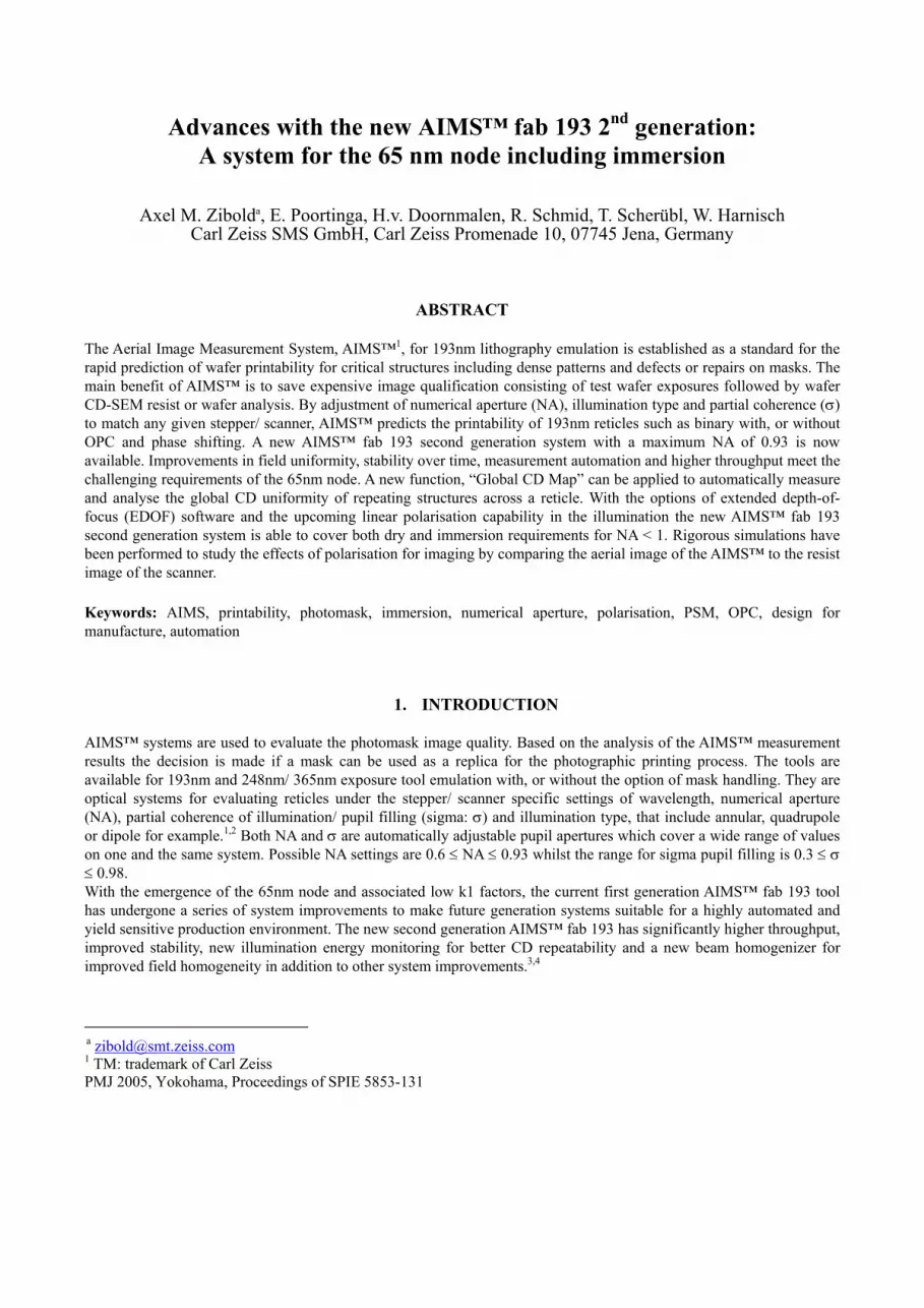
defocus or so-called Bossung plot and for further generalisation the exposure-defocus window are displayed. Effects are compared using an immersion liquid with refractive index n = 1.44 (water) and air with n = 1 in the space between wafer and scanner lens. At fixed threshold levels we can see in figure 7 that line width values can be found for larger focal values applying the immersion liquid. This already indicates an increase in the process window.
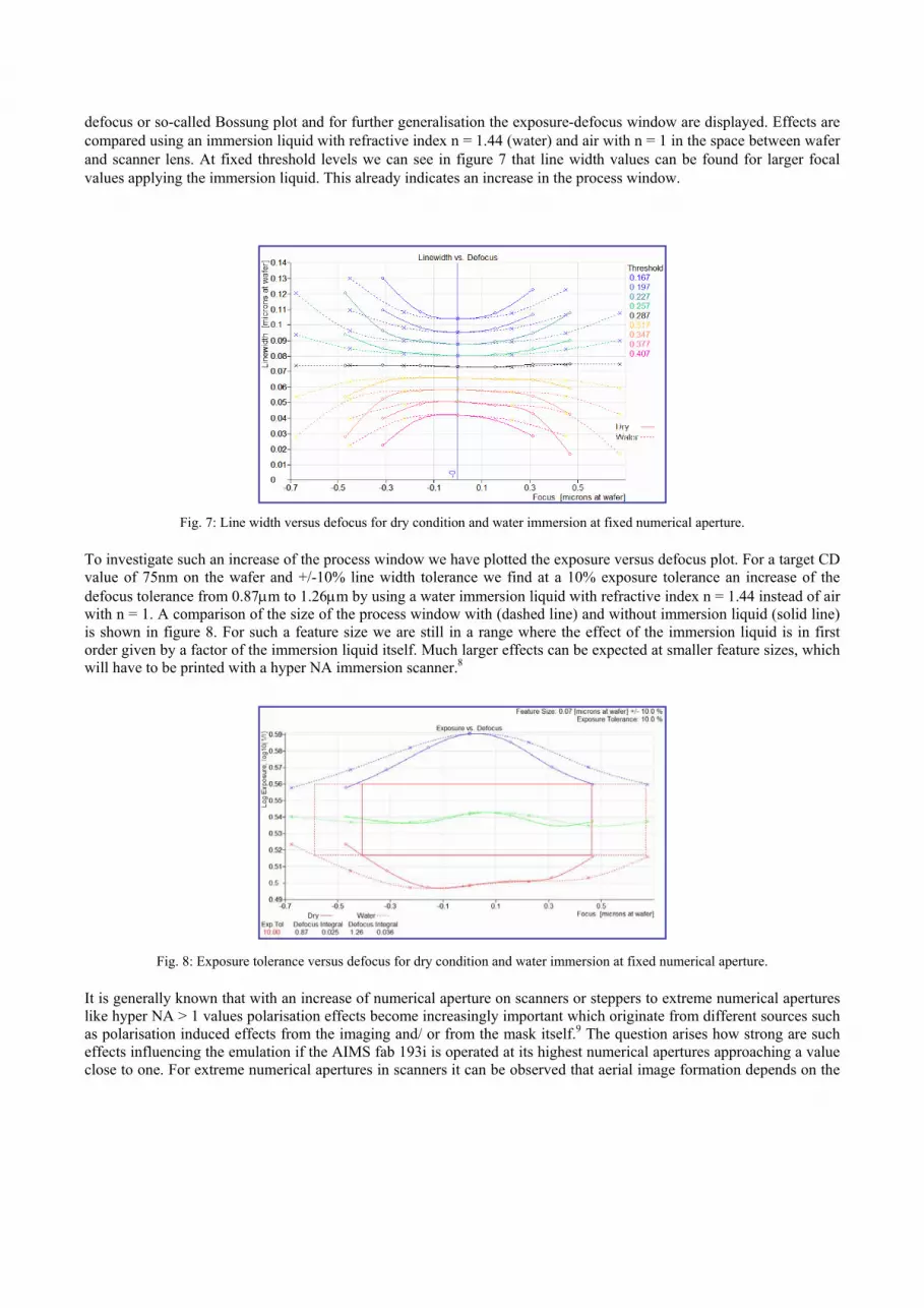
Fig. 7: Line width versus defocus for dry condition and water immersion at fixed numerical aperture. To investigate such an increase of the process window we have plotted the exposure versus defocus plot. For a target CD value of 75nm on the wafer and +/-10% line width tolerance we find at a 10% exposure tolerance an increase of the defocus tolerance from 0.87µm to 1.26µm by using a water immersion liquid with refractive index n = 1.44 instead of air with n = 1. A comparison of the size of the process window with (dashed line) and without immersion liquid (solid line) is shown in figure 8. For such a feature size we are still in a range where the effect of the immersion liquid is in first order given by a factor of the immersion liquid itself. Much larger effects can be expected at smaller feature sizes, which will have to be printed with a hyper NA immersion scanner.8
Fig. 8: Exposure tolerance versus defocus for dry condition and water immersion at fixed numerical aperture.
It is generally known that with an increase of numerical aperture on scanners or steppers to extreme numerical apertures like hyper NA > 1 values polarisation effects become increasingly important which originate from different sources such as polarisation induced effects from the imaging and/ or from the mask itself.9 The question arises how strong are such effects influencing the emulation if the AIMS fab 193i is operated at its highest numerical apertures approaching a value close to one. For extreme numerical apertures in scanners it can be observed that aerial image formation depends on the

sum of the TE (s-type) and TM (p-type) polarised images. For light with polarisation states in the plane of incidence, TM, a reduction in image contrast will result whereas for light with TE polarisation states no reduction in image contrast will be apparent. Considering the 1:4 reduction of the scanner or stepper and the 150x magnification on the AIMS™, the scanner is having large angles of incident light between resist and imaging optics (lens space), whereas the AIMS™ has much smaller angles of incident light on the CCD camera plane which is the equivalent image plane to capture the latent resist image. Therefore contrast loss at very large angles is not expected to be seen in the AIMS™ and has to be additionally emulated. However, important for printing is the angle of the interfering waves in the resist and therefore the appropriate comparison is always the aerial image of the AIMS™ to the resist image of the scanner. For NA < 1 independent of an immersion liquid or air in the lens space of an exposure tool numerical apertures in resist are << 1. Therefore polarisation effects in the resist are expected to be small compared to hyper NA and only an increased depth-of-focus should be considered. To investigate these polarisation issues for the AIMS™ fab 193i in more detail we have performed a series of different simulations using a rigorous coupled waves analysis simulation realised from an in-house simulation software of Carl Zeiss.7 This simulation takes the interaction of the electromagnetic field vectors and the three-dimensional structure of the mask features into account. The reflection and transmission behaviour on the interface between resist and medium of the lens space has also to be considered. The simulation parameters are shown in table 1. They are performed for both the scanner image latent in the resist and the aerial image of an AIMS™.
AIMS™ settings λ=193nm, NA = 0.92, sigma=0.7c Mask reduction 1:4 Mask type Chrome on quartz with AR coating Feature size 400nm Layer thickness Chrome 48.2nm
Anti-reflex coating 12.2nm Refractive Indices Anti-reflex coating n = 2.03 + i1.50
Chrome n = 1.12 + i1.95 Quartz n = 1.56 + i0.00
Resist: refractive index nR = 1.7 Table 1: Simulation parameters.
Fig. 9: Comparison of the aerial image results on AIMS™ and the resist image results of a scanner
for 400nm binary mask features.
Figure 9 compares an intensity profile plot for an aerial image result of AIMS™ with a resist image from a scanner for 400nm binary line and space mask features chrome on quartz. A very good match can be seen with the AIMS™ having slightly higher peak intensities compared to the scanner results. The TM polarisation states provide a slight contrast loss
0 20 40 60 80 10
0.6
a.u.
AIMSScanner
0
0.3

at the scanner thus we expect a larger contrast at the AIMS™. Figure 10 shows the relative difference of the line width between scanner and AIMS™ results versus threshold using a straight forward threshold model. Since the AIMS™ allows us to take through-focus images in order to provide the full lithographic information such as Bossung curves, process windows or process latitudes, we have the simulations for best focus and out of focal layers covering a third and two thirds of the depth-of-focus. We can see that for a wide range around the center threshold the CD results are matching very well. Therefore we can conclude that the CD criteria at intermediate thresholds are still a very good criteria for printability analysis in cases of high NA close to 1.
Fig. 10: Comparison of line width/ CD difference versus threshold results between AIMS™ scanner for 400nm binary mask features
An upcoming linear polariser in the illumination beam path of the AIMS™ fab 193i which can be used in addition to unpolarised illumination will provide a research capability for investigating the rigorous polarisation effects of masks. This will be a subject of further publications.
SUMMARY
The AIMS™ fab 193 second generation system is very suitable for scanner/ stepper emulation for both immersion and dry systems in the area of numerical apertures up to 0.93 for the 65nm node. An extended depth-of-focus software allows the emulation of effects from immersion liquids, whilst a linear polarised illumination capability is under development which will provide a research capability to investigate the rigorous polarisation effects of the mask itself. In this work we have presented advances with hardware and software. Especially, a new energy monitoring system and beam homogeniser that provide significantly improved field and pupil illumination uniformities and improved symmetry. A recipe based software operation enables easy operation, automatic tool set up to the lithography equivalent settings and allows automatic multiple point measurements. In addition the throughput is increased almost twofold. A software plug-in known as “Global CD Map” is now available to determine global CD uniformity with an automated measurement and evaluation routine. Rigorous coupled wave analysis simulation has shown a very good matching of AIMS™ and scanner results for such a NA < 1 system despite polarization effects arising from imaging. The deviations seen for maximum peak intensities indicate that criteria for printability results on AIMS™ have rather to be based on CD criteria at intermediate thresholds instead of transmission loss criteria as is commonly performed at larger nodes.
0.1 0
2%
4%
6%
threshold
delta CD BFDeltaCD 1/3 DOFDeltaCD 2/3 DOF
0.2 0.3 0.4

ACKNOWLEDGEMENT The authors would like to thank Oliver Kienzle, Mark Joyner, Klaus Böhm, Wolfgang Degel, Robert Birkner and Peter Schaeffer for their discussions and support related to the topics.
REFERENCES 1. R.A. Budd, D.B. Dove, J.L. Staples, R.M. Martino, R.A. Furguson, J.T. Weed. Development and application of a
new tool for lithographic mask evaluation, the stepper equivalent Aerial Image Measurement System, AIMS. IBM J. Res. Develop. Vol 41 No.1,2 January/ March, 1997.
2. R.A. Budd, J. Staples and D. B. Dove. A New Tool for Phase Shift Mask Evaluation, the Stepper Equivalent Aerial Image Measurement System AIMS. Proceedings of SPIE Vol. 2087, 1993.
3. A.M. Zibold, T. Scherübl, A. Menck, R. Brunner, J. Greif. Aerial Image Measurement Technique for Today’s and Future 193nm Lithography Mask Requirements. Proceedings of 20th EMC Conference, 2004.
4. A.M. Zibold, R. Schmid, B. Stegemann, T. Scheruebl, W. Harnisch, Y. Kobiyama. Aerial image measurement technique for Automated Reticle Defect Disposition (ARDD) in Wafer Fabs. Proceedings of SPIE Vol. 5446-117, 2004.
5. A.M. Zibold, R. Schmid, K. Böhm, R. Birkner. Aerial Image Measuring System at 193nm – a tool to tool comparison and global CD mapping. Proceedings of SPIE Vol. 5567-118, 2004.
6. A.M. Zibold, R. Schmid, A. Seyfarth, M. Wächter, W. Harnisch, H.v. Doornmalen. Advances in hardware, software and automation for 193nm aerial image measurement systems. Proceedings of SPIE Vol. 5752-114, 2004.
7. A. Zibold, W. Harnisch, T. Scherübl, N. Rosenkranz, J. Greif. Using the aerial image measurement technique to speed up mask development for 193nm immersion and polarization lithography. Proceedings of SPIE Vol. 5645-30, 2004.
8. C.A. Mack and J.D. Byers. Exploring the Capabilities of Immersion Lithography Through Simulation. Proceedings of SPIE Vol. 5377, 2004.
9. B.W. Smith, L. Zavyalova, A. Estroff. Benefiting from polarization – effects on high-NA imaging. Proceedings of SPIE Vol. 5377, 2004.