system integration and performance of the euv engineering test stand
TRANSCRIPT

Approved for public release; further dissemination unlimited
PreprintUCRL-JC-143203
System Integration andPerformance of the EUVEngineering Test Stand
D. A. Tichenor, A. K. Ray-Chaudhuri, W. C. Replogle, R.H. Stulen, G. D. Kubiak, P. D. Rockett, L. E. Klebanoff, K.L. Jefferson, A. H. Leung, J. B. Wronosky, L. C. Hale, H.N. Chapman, J. S. Taylor, J. A. Folta, C. Montcalm, R.Soufli, E. Spiller, K. Blaedel, G. E. Sommargren, D. W.Sweeney, P. Naulleau, K. A. Goldberg, E. M. Gullikson, J.Bokor, P. J. Batson, D. T. Attwood, K. H. Jackson, S. D.Hector, C. W. Gwyn, and P-Y. Yan
This article was submitted toThe International Society for Optical Engineering 26th InternationalSymposium on Microlithography Emerging Lithographies, SantaClara, California, February 25 – March 2, 2001
March 23, 2001
LawrenceLivermoreNationalLaboratory
U.S. Department of Energy

DISCLAIMER This document was prepared as an account of work sponsored by an agency of the United StatesGovernment. Neither the United States Government nor the University of California nor any of theiremployees, makes any warranty, express or implied, or assumes any legal liability or responsibility forthe accuracy, completeness, or usefulness of any information, apparatus, product, or process disclosed, orrepresents that its use would not infringe privately owned rights. Reference herein to any specificcommercial product, process, or service by trade name, trademark, manufacturer, or otherwise, does notnecessarily constitute or imply its endorsement, recommendation, or favoring by the United StatesGovernment or the University of California. The views and opinions of authors expressed herein do notnecessarily state or reflect those of the United States Government or the University of California, andshall not be used for advertising or product endorsement purposes. This is a preprint of a paper intended for publication in a journal or proceedings. Since changes may bemade before publication, this preprint is made available with the understanding that it will not be citedor reproduced without the permission of the author.
This report has been reproduced directly from the best available copy.
Available electronically at http://www.doc.gov/bridge
Available for a processing fee to U.S. Department of Energy And its contractors in paper from
U.S. Department of Energy Office of Scientific and Technical Information
P.O. Box 62 Oak Ridge, TN 37831-0062 Telephone: (865) 576-8401 Facsimile: (865) 576-5728
E-mail: [email protected]
Available for the sale to the public from U.S. Department of Commerce
National Technical Information Service 5285 Port Royal Road Springfield, VA 22161
Telephone: (800) 553-6847 Facsimile: (703) 605-6900
E-mail: [email protected] Online ordering: http://www.ntis.gov/ordering.htm
OR
Lawrence Livermore National Laboratory Technical Information Department’s Digital Library
http://www.llnl.gov/tid/Library.html
1
System Integration and Performance of the EUV Engineering Test Stand
Daniel A. Tichenor*a, Avijit K. Ray-Chaudhuria, William C. Reploglea,Richard H. Stulena, Glenn D. Kubiaka, Paul D. Rockett a, Leonard E. Klebanoffa,
Karen L. Jeffersona, Alvin H. Leunga, John B. Wronoskyb, Layton C. Halec,Henry N. Chapmanc, John S. Taylorc, James A. Foltac, Claude Montcalmc,Regina Souflic, Eberhard Spillerc, Kenneth Blaedelc, Gary E. Sommargrenc,
Donald W. Sweeneyc, Patrick Naulleaud, Kenneth A. Goldbergd, Eric M. Gulliksond,Jeffrey Bokord, Phillip J. Batsond, David T. Attwoodd, Keith H. Jacksond,
Scott D. Hectore, Charles W. Gwynf, and Pei-Yang Yanf,
aSandia National Laboratories, PO Box 969, Livermore CA 94551bSandia National Laboratories, PO Box 5800, Albuquerque NM 87185
cLawrence Livermore National Laboratory, PO Box 808, Livermore, CA 94550dLawrence Berkeley National Laboratory, One Cyclotron Road, Berkeley, CA 94720
eMotorola Corporation, 3501 Ed Bluestein Blvd, Austin TX 78721fIntel Corporation, 2200 Mission College Boulevard, Santa Clara CA 95052
ABSTRACTThe Engineering Test Stand (ETS) is a developmental lithography tool designed to demonstrate full-field EUV imaging andprovide data for commercial-tool development. In the first phase of integration, currently in progress, the ETS is configuredusing a developmental projection system, while fabrication of an improved projection system proceeds in parallel. The opticsin the second projection system have been fabricated to tighter specifications for improved resolution and reduced flare. Theprojection system is a 4-mirror, 4x-reduction, ring-field design having a numeral aperture of 0.1, which supports 70 n mresolution at a k1 of 0.52. The illuminator produces 13.4 nm radiation from a laser-produced plasma, directs the radiationonto an arc-shaped field of view, and provides an effective fill factor at the pupil plane of 0.7. The ETS is designed for full-field images in step-and-scan mode using vacuum-compatible, magnetically levitated, scanning stages. This paper describessystem performance observed during the first phase of integration, including resist images of 100 nm isolated and densefeatures.
Keywords: EUVL, lithography, multilayer coatings, optical fabrication, optical design, laser-produced plasma, laser plasmasource, maglev, magnetic levitation, stages, precision engineering
1. INTRODUCTION
During the past year Extreme Ultraviolet Lithography (EUVL) has become widely viewed as the leading next-generation-lithography candidate for dense features down to 30 nm with introduction as early as the 70 nm node. An alpha-class tool,called the EUV Engineering Test Stand (ETS), has been developed to demonstrate full-field printing of EUV images and todevelop the system learning required to commercialize EUVL technology1. The ETS is designed to meet the system learningobjectives at critical dimensions in the 70 nm to 100 nm range. In a parallel effort, a micro-exposure tool2 (MET) is beingdeveloped to study EUV imaging down to 30 nm and provide a test bed for resist development. Advancement in multilayercoatings for 13.4 nm radiation is the enabling technology that supports all-reflective projection systems for the ETS andproduction tools designed to operate in step-and-scan mode. EUVL technology development is funded by the EUV LimitedLiability Company (LLC), a consortium of semiconductor manufacturers founded in 1997 and comprised of Advanced MicroDevices, Infineon, Intel, IBM, Micron, and Motorola. The Department of Energy Virtual National Laboratory, comprised ofLawrence Berkeley National Laboratory, Lawrence Livermore National Laboratory and Sandia National Laboratories,perform research, development, and engineering to accelerate the commercialization of EUVL.
The Virtual National Laboratory has been working to an accelerated schedule during the past year with the objective ofbringing the ETS on line six months ahead of the originally planned operation date. The ETS has completed the subsystem-qualification and system-assembly phases and is currently operational in static imaging mode. Tool-setup parameters, such
_________________________* Correspondence: Email: [email protected]; Telephone: 925 294 2137; Fax: 925 294 3870
2
as exposure time, stage skew, scan magnification and focal plane location, are being determined by printing static images andcharacterizing the results using scanning electron microscopy and high-resolution wafer metrology. This paper reviewsprogress during the past year in the supporting technologies, subsystem development, and system integration. Initial resultsfrom tool-setup experiments in which 100 nm isolated and dense features are printed in photoresist are described.
2. ETS DESIGN AND INTEGRATION
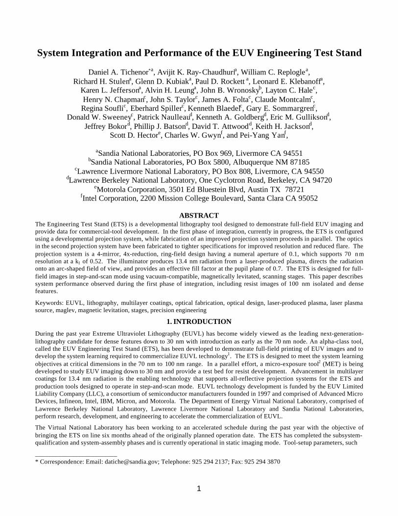
2.1 System design overviewThe ETS is comprised of two major environmental enclosures, the source chamber that houses the laser-produced plasma(LPP) source and illumination system, and the main chamber that houses the projection optics and stage system (See Fig. 1).The EUV radiation is generated by focusing a pulsed Nd:YAG laser beam onto a xenon-cluster target, which is supported bya xenon re-circulation system. A six-channel condenser collects radiation from the source and directs it into the mainchamber, where a final condenser element shapes the beam to illuminate the arc-shaped field of view of the projectionsystem. A membrane-type spectral-purity filter removes out-of-band radiation and provides an environmental barrierbetween the source and main chambers.
Figure 1. Solid model of the EUV Engineering Test Stand.
The projection system is a 4-mirror, 4x-reduction system having a numerical aperture of 0.1 and is designed for printing full-field images in step-and-scan mode. This design is capable of printing 70 nm dense features at a k1 value of 0.52. Thecurrent phase of ETS integration and characterization uses a developmental projection system, while the final projectionsystem is being assembled and aligned in parallel for installation later this year.
The scanning stage system provides a full 6-degrees of freedom for both the wafer and reticle using magnetic levitation(maglev) technology. A linear motor drives one axis of each stage in the scanning direction, while a set of magnetic actuatorsenables control of the remaining 5 degrees of freedom over short travel ranges. In the cross-scan direction, a mechanicallead-screw-driven stage provides the travel range needed to cover all sites on a 200 mm wafer. A system of capacitivesensors and laser gauges feeds back the actuator gaps and stage position required for the digital control system to executestage movements and to maintain stage synchronization. Vacuum compatible vibration isolators support the projection
3
system and stage metrology, while grounded structures support the reticle and wafer stage bases. The levitated reticle andwafer platens are isolated from ground vibrations through feedback control.
2.2 System integrationDevelopment and testing of the three major subsystems, illuminator, projection optics box, and stages, were performed inparallel prior to integration. The illuminator, comprised of the source, a multi-element condenser and an environmentalenclosure, was assembled in its final location in the ETS laboratory and tested in place using a 40 watt, Coherent InfinityNd:YAG laser. The resulting EUV illumination beam was directed into a diagnostic chamber in which the illumination at thereticle plane and projection-system pupil plane were measured and characterized. ETS integration is progressing using thissource, while the high-power source, driven by a 1700 watt TRW Inc. Nd :YAG laser, is being developed in parallel. Thecapability to operate with either laser has been implemented to facilitate source-power upgrade.
The projection system was assembled and aligned using a developmental set of aspheric mirrors. This projection system, POBox 1, is installed in the ETS for initial system learning, while the final projection system, PO Box 2, containing mirrors thatmeet the ETS specifications, is being assembled and tested. PO Box 1 has undergone extensive testing at the actinicwavelength3.
The wafer and reticle stages were tested with their respective metrology systems on alignment stations designed to verifymechanical alignment and test stage control hardware and software. For each stage the metrology system, comprised of themetrology laser, distance-measuring interferometers, and associated beam splitters and beam benders, were installed andaligned on structures called metrology trays. In the ETS the metrology trays are referenced to each other through a low-expansion structure called the isolated frame.
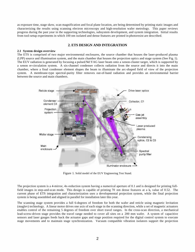
The main chamber was assembled and characterized in a space adjacent to the ETS laboratory while the illuminator wasundergoing testing. The structural components, including the polymer-concrete pedestal, the stage bridge that supports thereticle stage, the vibration isolation system, and the isolated frame, were installed using mass surrogates for the metrologytrays and the PO Box to achieve the design weight of 1090 Kg (2400 pounds) required for the coil-spring passive isolators.In this configuration the vibration isolation system performance was tested in the passive/active isolation mode (See Fig. 2).
Figure 2. Vibration isolation system installed. Transmissibility curves show improved performancewith active damping.
The PO Box was installed through the top hatch of the main chamber, engaging the isolated frame by means of a kinematicinterface. Object and image plane sensors, comprised of six capacitance gauges and two video microscopes, define thedesired locations of the reticle and wafer planes, respectively, as determined during the final alignment procedure. Thereticle stage and metrology tray were installed through the top hatch, and the wafer stage and metrology tray were installedthrough a side port, using kinematic mounts for all four components. System alignment procedures were carried out to adjust
4
the stages and isolated frame to bring the reticle and wafer planes into alignment with the PO Box as determined by theobject and image plane sensors. Kinematic mounts enable the removal and re-installation of the PO Box and stagecomponents without the need to repeat the system alignment procedure. Customized handling equipment was designed andbuilt to facilitate the installation of these components.
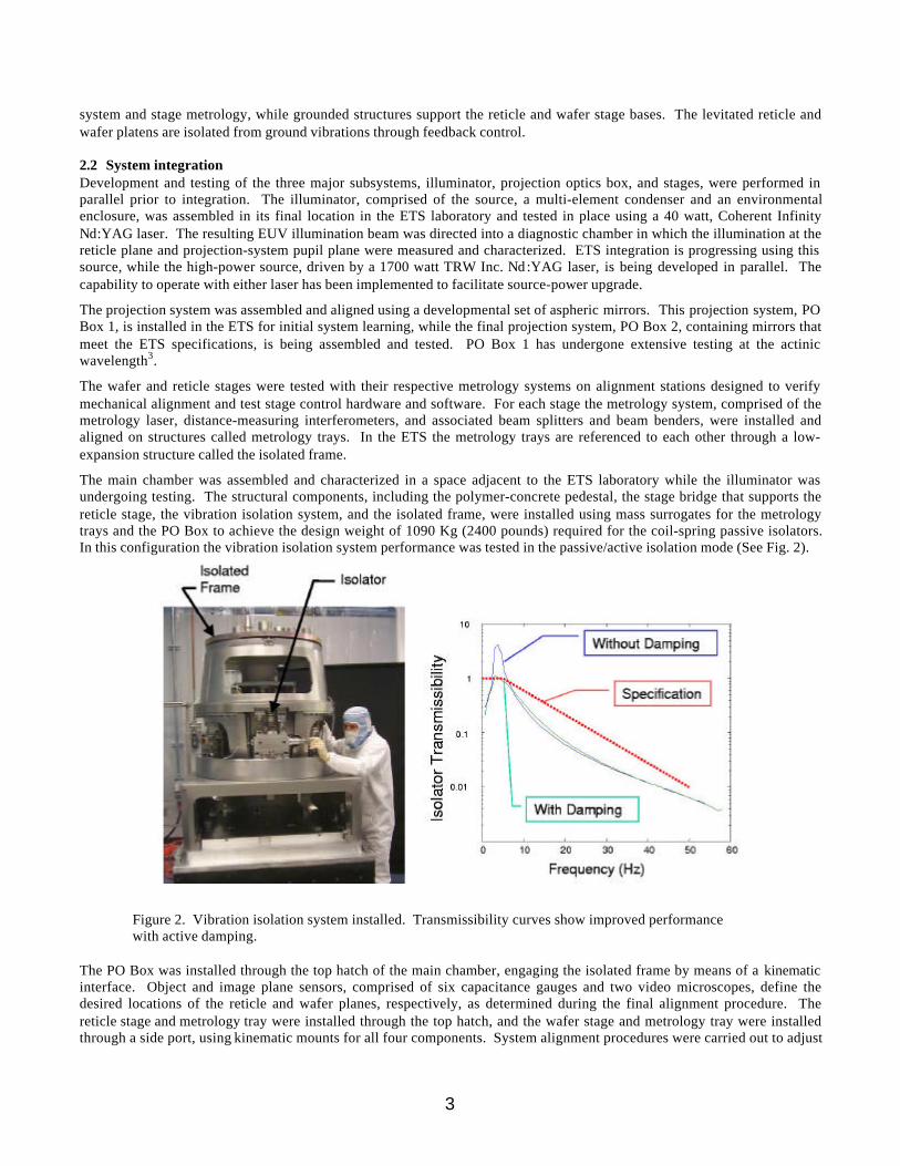
The ETS is extensively equipped with sensors to gather data in support of the system-learning role. Approximately 62temperature sensors, 23 vibration sensors and 21 EUV flux sensors are installed in the ETS. In addition, the ETS contains anumber of custom sensors, including source position sensors, a Through-The-Lens Imager (TTLI), an aperture viewingsensor, a reticle dose sensor array, a wafer dose sensor and an Aerial Image Monitor (AIM). The TTLI comprises a visible-light illuminator, custom microscope lens and an external video camera (See Fig. 3). The TTLI illuminator couples lightfrom a remote mercury-arc lamp into an optical fiber that carries the light to an illuminator lens mounted on the mainchamber. The light is injected through an optical port and reflects off a moveable folding mirror that is inserted upstream ofthe C4 mirror. Following the EUV path, the visible light beam reflects off the reticle, and the PO Box casts an image of thereticle onto the wafer. Light reflecting off the wafer is intercepted by a scraper mirror, located 75 mm above the wafer, anddirected to the TTLI imaging lens, which then casts the superimposed image of the reticle and wafer through an optical portto an external video camera. The resultant image is shown in Figure 3. This system is used to verify system alignment,locate features on the reticle, and to perform coarse alignment between reticle and wafer.
Figure 3. A schematic of the TTLI (left). Superimposed image of reticle and wafer features acquired in the ETS using the TTLI (right).
An aperture viewing system provides images of the EUV fill profile at the pupil of the PO Box. This diagnostic is used tocharacterize the fill profile and to perform final alignment of the illuminator. The pupil image is obtained by using an in-vacuum actuator to insert a scintillating screen of gadolinium oxysulfide into the EUV path just above the PO Box aperturestop on the M3 mirror. EUV radiation falling on the scintillating screen produces a visible-light image that is viewed througha mirror, located above the scintillating screen and to the side of the EUV path. The image is acquired using a video camera,which views the scintillating screen through an optical port in the main chamber.
EUV sensors located on the wafer and reticle stages perform measurements of dose uniformity at the wafer and reticle plane.In addition, an AIM sensor can be used to characterize projection-system and stage performance. These sensors are based onan EUV-sensitive photodiode, coated with zirconium to eliminate out-of-band radiation. On the reticle stage, a one-dimensional array of 80 photodiodes is scanned through the field of view to acquire an image of the reticle illumination. Onthe wafer stage a single photodiode is used in each of two sensors, the dose sensor and the AIM sensor, which can bepositioned in a two-dimensional field. These sensors are identical except for the EUV-transparent artifact located above thephotodiode. A 25 micron pinhole is used for the wafer dose sensor, and a series of narrow slits is used in the AIM sensor toanalyze small features imaged from the reticle. For all of these sensors, the EUV signals are acquired and digitized insideelectrically shielded enclosures on board the stages to mitigate electromagnetic interference from the plasma source. The datais transmitted digitally to the external sensor controller after the source pulse interference has decayed.
After completion of stage performance testing in the main chamber, the stages and PO Box were removed, and the mainchamber assembly was transported into the ETS laboratory using air castors (see Fig. 4). A system alignment procedure was
Featureson wafer
Featureson reticle

5
performed to bring the two chambers into alignment and to assure that the illumination beam is incident on the well-correctedfield of view of the PO Box. In the new location a number of diagnostic tests were performed to verify stages-to-PO Boxalignment, vibration-isolation system performance, stage system performance, TTLI alignment and vacuum systemfunctionality.
Figure 4. The main chamber (left) being aligned to the source chamber (right).
After these tests were completed, the wafer robot was installed and taught the wafer loading position, thus providing thecapability to load and unload wafers without breaking vacuum. The additional controls functionality required for initial tool-setup experiments was implemented, including the acquisition of data from the aperture viewing system, TTLI, temperaturesensors and vibration sensors. The initial functionality also includes the acquisition of flux data from in-band detectorslocated at the first condenser element, C1, and from EUV mirrors throughout the system, which carry a 10 volt negative biasand operate as photo-emission detectors. Finally, the function of moving the stage to positions for focus-exposure matriceswas implemented together with the ability to execute static exposures while controlling dose by counting pulses or byintegrating the flux measured at the final condenser element, C4.
3. ENVIRONMENTAL SUBSYSTEM
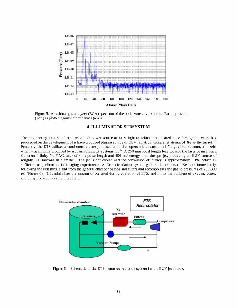
The first environmental data from the ETS has been collected and is shown in Figure 5 for the “Optic Zone” of the MainChamber. Excellent control of high-mass hydrocarbons has been achieved. This control is a result of extensive outgastesting and screening of components and materials to minimize high mass (>44 amu) hydrocarbons. Furthermore, attentionwas paid to vacuum compatible design of the ETS, careful cleaning of parts, pre-baking of cables and subassemblies wherepossible, and clean assembly procedures. As a result of the hydrocarbon control, the residual ETS vacuum environment isrich in water vapor, as indicated in Figure 5. Analysis of witness plate data indicates that the ETS environment does not posea contamination risk to the optics in the absence of EUV irradiation. However, with EUV exposure, the water richenvironment can lead to EUV-induced water oxidation of the Si-terminated Mo/Si optics. It was found that added ethanolcan prevent optic oxidation, allowing carbon growth via EUV “cracking” of low-level residual hydrocarbons. The EUVenvironmental issues are understood, mitigation approaches have been validated, and EUV optic contamination appears to bemanageable. Further data concerning the ETS environment can be found in the paper by Klebanoff et al. in theseproceedings4.
6
Figure 5. A residual gas analyzer (RGA) spectrum of the optic zone environment. Partial pressure(Torr) is plotted against atomic mass (amu).
4. ILLUMINATOR SUBSYSTEM
The Engineering Test Stand requires a high-power source of EUV light to achieve the desired EUV throughput. Work hasproceeded on the development of a laser-produced plasma source of EUV radiation, using a jet stream of Xe as the target.5-7
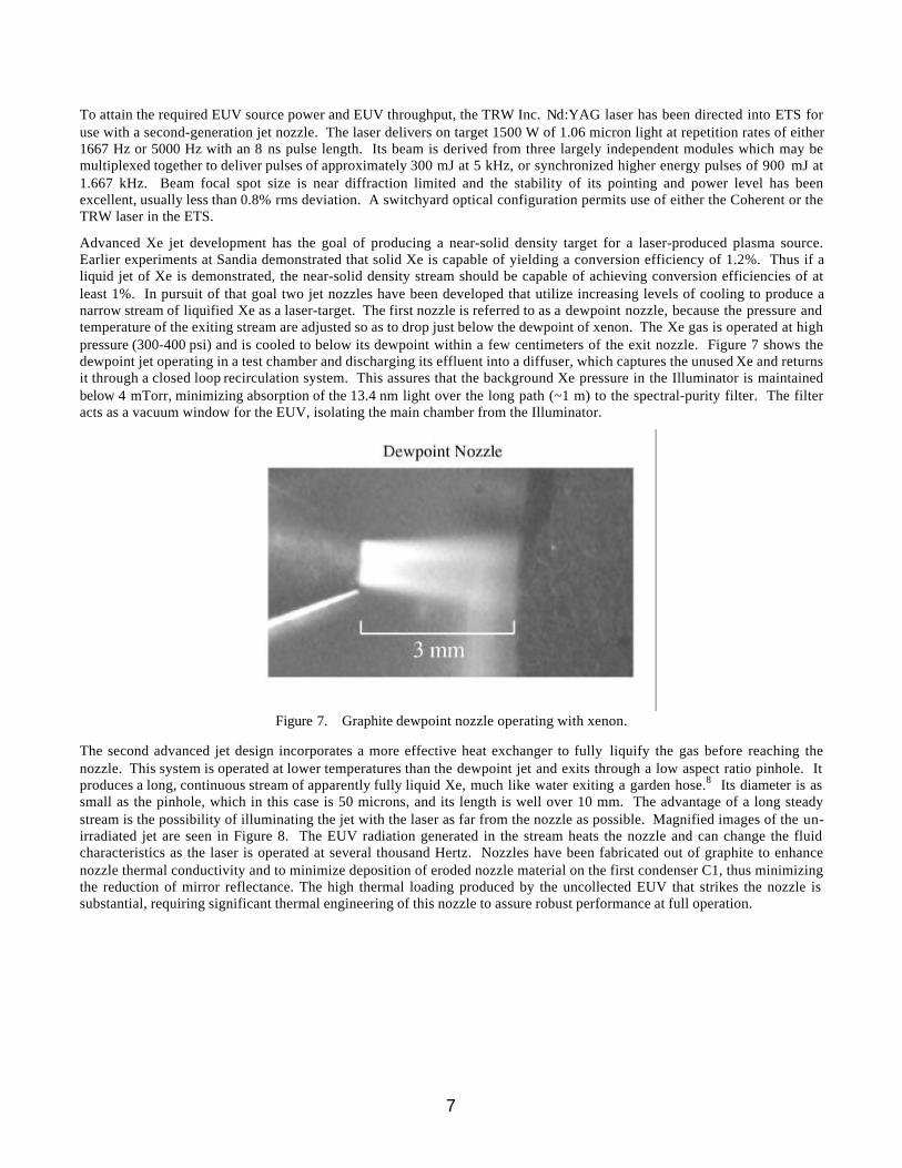
Presently, the ETS utilizes a continuous cluster-jet based upon the supersonic expansion of Xe gas into vacuum, a nozzlewhich was initially produced by Advanced Energy Systems Inc.5 A 250 mm focal length lens focuses the laser beam from aCoherent Infinity Nd:YAG laser of 4 ns pulse length and 400 mJ energy onto the gas jet, producing an EUV source ofroughly 300 microns in diameter. The jet is not cooled and the conversion efficiency is approximately 0.1%, which issufficient to perform initial imaging experiments. A Xe recirculation system gathers the exhausted Xe both immediatelyfollowing the exit nozzle and from the general chamber pumps and filters and recompresses the gas to pressures of 200-300psi (Figure 6). This minimizes the amount of Xe used during operation of ETS, and limits the build-up of oxygen, water,and/or hydrocarbons in the Illuminator.
Figure 6. Schematic of the ETS xenon recirculation system for the EUV jet source.
7
To attain the required EUV source power and EUV throughput, the TRW Inc. Nd:YAG laser has been directed into ETS foruse with a second-generation jet nozzle. The laser delivers on target 1500 W of 1.06 micron light at repetition rates of either1667 Hz or 5000 Hz with an 8 ns pulse length. Its beam is derived from three largely independent modules which may bemultiplexed together to deliver pulses of approximately 300 mJ at 5 kHz, or synchronized higher energy pulses of 900 mJ at1.667 kHz. Beam focal spot size is near diffraction limited and the stability of its pointing and power level has beenexcellent, usually less than 0.8% rms deviation. A switchyard optical configuration permits use of either the Coherent or theTRW laser in the ETS.
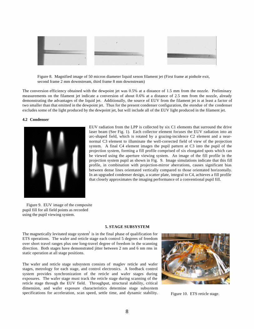
Advanced Xe jet development has the goal of producing a near-solid density target for a laser-produced plasma source.Earlier experiments at Sandia demonstrated that solid Xe is capable of yielding a conversion efficiency of 1.2%. Thus if aliquid jet of Xe is demonstrated, the near-solid density stream should be capable of achieving conversion efficiencies of atleast 1%. In pursuit of that goal two jet nozzles have been developed that utilize increasing levels of cooling to produce anarrow stream of liquified Xe as a laser-target. The first nozzle is referred to as a dewpoint nozzle, because the pressure andtemperature of the exiting stream are adjusted so as to drop just below the dewpoint of xenon. The Xe gas is operated at highpressure (300-400 psi) and is cooled to below its dewpoint within a few centimeters of the exit nozzle. Figure 7 shows thedewpoint jet operating in a test chamber and discharging its effluent into a diffuser, which captures the unused Xe and returnsit through a closed loop recirculation system. This assures that the background Xe pressure in the Illuminator is maintainedbelow 4 mTorr, minimizing absorption of the 13.4 nm light over the long path (~1 m) to the spectral-purity filter. The filteracts as a vacuum window for the EUV, isolating the main chamber from the Illuminator.
Figure 7. Graphite dewpoint nozzle operating with xenon.
The second advanced jet design incorporates a more effective heat exchanger to fully liquify the gas before reaching thenozzle. This system is operated at lower temperatures than the dewpoint jet and exits through a low aspect ratio pinhole. Itproduces a long, continuous stream of apparently fully liquid Xe, much like water exiting a garden hose.8 Its diameter is assmall as the pinhole, which in this case is 50 microns, and its length is well over 10 mm. The advantage of a long steadystream is the possibility of illuminating the jet with the laser as far from the nozzle as possible. Magnified images of the un-irradiated jet are seen in Figure 8. The EUV radiation generated in the stream heats the nozzle and can change the fluidcharacteristics as the laser is operated at several thousand Hertz. Nozzles have been fabricated out of graphite to enhancenozzle thermal conductivity and to minimize deposition of eroded nozzle material on the first condenser C1, thus minimizingthe reduction of mirror reflectance. The high thermal loading produced by the uncollected EUV that strikes the nozzle issubstantial, requiring significant thermal engineering of this nozzle to assure robust performance at full operation.
8
Figure 8. Magnified image of 50 micron diameter liquid xenon filament jet (First frame at pinhole exit,second frame 2 mm downstream, third frame 8 mm downstream)
The conversion efficiency obtained with the dewpoint jet was 0.5% at a distance of 1.5 mm from the nozzle. Preliminarymeasurements on the filament jet indicate a conversion of about 0.6% at a distance of 2.5 mm from the nozzle, alreadydemonstrating the advantages of the liquid jet. Additionally, the source of EUV from the filament jet is at least a factor oftwo smaller than that emitted in the dewpoint jet. Thus for the present condenser configuration, the etendue of the condenserexcludes some of the light produced by the dewpoint jet, but will include all of the EUV light produced in the filament jet.
4.2 Condenser
EUV radiation from the LPP is collected by six C1 elements that surround the drivelaser beam (See Fig. 1). Each collector element focuses the EUV radiation into anarc-shaped field, which is rotated by a grazing-incidence C2 element and a near-normal C3 element to illuminate the well-corrected field of view of the projectionsystem. A final C4 element images the pupil pattern at C3 into the pupil of theprojection system, forming a fill profile comprised of six elongated spots which canbe viewed using the aperture viewing system. An image of the fill profile in theprojection system pupil as shown in Fig. 9. Image simulations indicate that this fillprofile, in combination with projection-mirror aberrations, causes significant biasbetween dense lines orientated vertically compared to those orientated horizontally.In an upgraded condenser design, a scatter plate, integral to C4, achieves a fill profilethat closely approximates the imaging performance of a conventional pupil fill.
Figure 9. EUV image of the compositepupil fill for all field points as recordedusing the pupil viewing system.
5. STAGE SUBSYSTEM
The magnetically levitated stage system1 is in the final phase of qualification forETS operations. The wafer and reticle stage each control 5 degrees of freedomover short travel ranges plus one long-travel degree of freedom in the scanningdirection. Both stages have demonstrated jitter between 2 nm and 6 nm rms instatic operation at all stage positions.
The wafer and reticle stage subsystem consists of maglev reticle and waferstages, metrology for each stage, and control electronics. A feedback controlsystem provides synchronization of the reticle and wafer stages duringexposures. The wafer stage must track the reticle stage during scanning of thereticle stage through the EUV field. Throughput, structural stability, criticaldimension, and wafer exposure characteristics determine stage subsystemspecifications for acceleration, scan speed, settle time, and dynamic stability. Figure 10. ETS reticle stage.

9
The ETS requires that jitter for each stage as referenced to the PO box always be less than 10 nm rms and that the meantracking error be less than ±3nm9. Performance to these specifications has been demonstrated in the ETS. Figures 10 and 11show the reticle and wafer stages installed in the ETS.
5.1 Stage subsystem progress during 2000
Since first operation of the development wafer stage in late 1999, the EUV program has integrated the vacuum-compatiblewafer and reticle stages into the ETS. Fabrication and installation of the stage computer control system and electronics hasbeen completed. Changes have been made to both the stage hardware and the control electronics and software to incorporateknowledge gained through operation and analysis.
The stage concept was modified to accommodate an accelerated ETStesting schedule and performance issues relating to the cable stagedesign. The cable stage is included in the overall design concept tominimize position disturbances caused by cable forces seen by theplaten. The cable stage has been removed for early imaging. This ispossible due to reduced scanning velocity requirements for first imagingexperiments. Corrections to the design will be implemented over thenext year.
Electrical noise concerns dictated greater attention to signalmanagement in the control electronics. The evolution includes customVME bus signal management and custom signal conditioning for thehigh-speed (MHz) position measurement electronics.
Figure 11. ETS wafer stage.
5.2 Performance results
Evaluation of the stage performance in the ETS for first imaging experiments has been completed. The results are acceptablefor positioning of the reticle and wafer for EUV imaging. Both static and scanning performance measurements are shown.Figure 12 shows static jitter of each stage over its travel range. Figure 13 represents the combination of the wafer and reticlestage jitter and can be used to predict image blur. Figures 14 and 15 show scanning performance of the development waferstage operating without the cable stage at velocities required for early imaging experiments. Stage and system performancewill evolve with ongoing system analysis and operational experience.
Figure 12. Wafer and reticle stage static stability. The inner ellipses represent the measured jitter. The outter circlesrepresent the specified maximum jitter.

10
Figure 13. Stage contributions to image blur.
-180 -160 -140 -120 -100 -80 -60 -40 -20 0-3
-2
-1
0
1
2
3Reticle Mean Error Scanning at 2.0 mm/sec
Y Position (m)
Mea
n E
rror
(nm
)
XY
-180 -160 -140 -120 -100 -80 -60 -40 -20 00
2
4
6
8
10Reticle Jitter Scanning at 2.0 mm/sec
Y Position (m)
Jitte
r (nm
)
XY
Figure 14. Reticle stage scanning performance at 2.0mm/sec.
11
0 5 10 15 20 25 30 35 40 45-3
-2
-1
0
1
2
3Wafer Mean Error Scanning at 0.5 mm/sec
Y Position (m)
Mea
n E
rror
(nm
)
XY
0 5 10 15 20 25 30 35 40 450
2
4
6
8
10Wafer Jitter Scanning at 0.5 mm/sec
Y Position (m)
Jitte
r (nm
)
XY
Figure 15. Wafer stage scanning performance at 0.5 mm/sec.
6. PROJECTION SUBSYSTEM
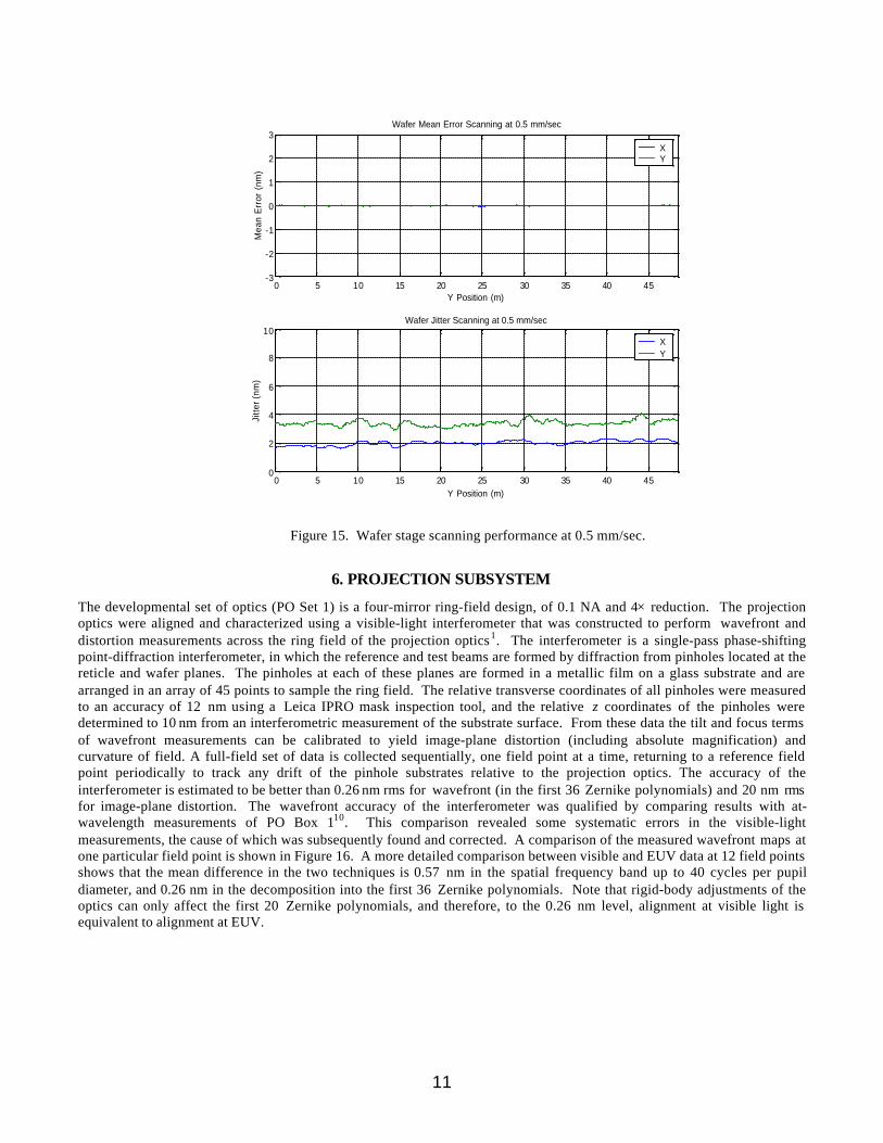
The developmental set of optics (PO Set 1) is a four-mirror ring-field design, of 0.1 NA and 4× reduction. The projectionoptics were aligned and characterized using a visible-light interferometer that was constructed to perform wavefront anddistortion measurements across the ring field of the projection optics1. The interferometer is a single-pass phase-shiftingpoint-diffraction interferometer, in which the reference and test beams are formed by diffraction from pinholes located at thereticle and wafer planes. The pinholes at each of these planes are formed in a metallic film on a glass substrate and arearranged in an array of 45 points to sample the ring field. The relative transverse coordinates of all pinholes were measuredto an accuracy of 12 nm using a Leica IPRO mask inspection tool, and the relative z coordinates of the pinholes weredetermined to 10 nm from an interferometric measurement of the substrate surface. From these data the tilt and focus termsof wavefront measurements can be calibrated to yield image-plane distortion (including absolute magnification) andcurvature of field. A full-field set of data is collected sequentially, one field point at a time, returning to a reference fieldpoint periodically to track any drift of the pinhole substrates relative to the projection optics. The accuracy of theinterferometer is estimated to be better than 0.26 nm rms for wavefront (in the first 36 Zernike polynomials) and 20 nm rmsfor image-plane distortion. The wavefront accuracy of the interferometer was qualified by comparing results with at-wavelength measurements of PO Box 110. This comparison revealed some systematic errors in the visible-lightmeasurements, the cause of which was subsequently found and corrected. A comparison of the measured wavefront maps atone particular field point is shown in Figure 16. A more detailed comparison between visible and EUV data at 12 field pointsshows that the mean difference in the two techniques is 0.57 nm in the spatial frequency band up to 40 cycles per pupildiameter, and 0.26 nm in the decomposition into the first 36 Zernike polynomials. Note that rigid-body adjustments of theoptics can only affect the first 20 Zernike polynomials, and therefore, to the 0.26 nm level, alignment at visible light isequivalent to alignment at EUV.
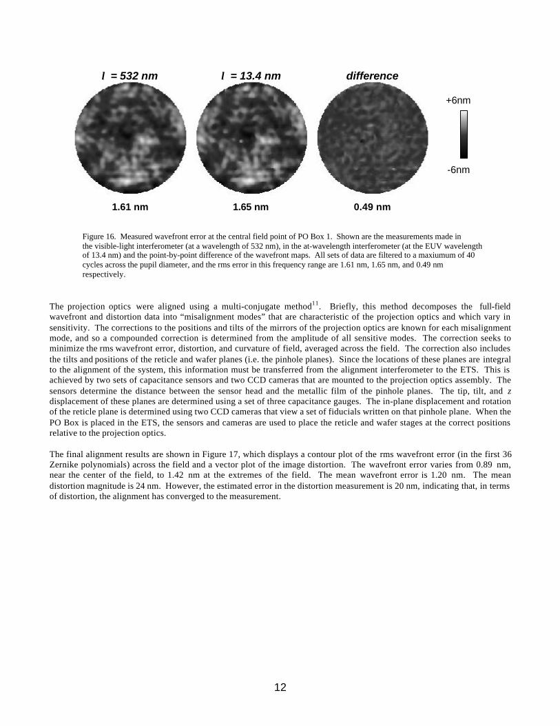
12
1.61 nm 1.65 nm 0.49 nm
λ = 532 nm λ = 13.4 nm difference
-6nm
+6nm
Figure 16. Measured wavefront error at the central field point of PO Box 1. Shown are the measurements made inthe visible-light interferometer (at a wavelength of 532 nm), in the at-wavelength interferometer (at the EUV wavelengthof 13.4 nm) and the point-by-point difference of the wavefront maps. All sets of data are filtered to a maxiumum of 40cycles across the pupil diameter, and the rms error in this frequency range are 1.61 nm, 1.65 nm, and 0.49 nmrespectively.
The projection optics were aligned using a multi-conjugate method11. Briefly, this method decomposes the full-fieldwavefront and distortion data into “misalignment modes” that are characteristic of the projection optics and which vary insensitivity. The corrections to the positions and tilts of the mirrors of the projection optics are known for each misalignmentmode, and so a compounded correction is determined from the amplitude of all sensitive modes. The correction seeks tominimize the rms wavefront error, distortion, and curvature of field, averaged across the field. The correction also includesthe tilts and positions of the reticle and wafer planes (i.e. the pinhole planes). Since the locations of these planes are integralto the alignment of the system, this information must be transferred from the alignment interferometer to the ETS. This isachieved by two sets of capacitance sensors and two CCD cameras that are mounted to the projection optics assembly. Thesensors determine the distance between the sensor head and the metallic film of the pinhole planes. The tip, tilt, and zdisplacement of these planes are determined using a set of three capacitance gauges. The in-plane displacement and rotationof the reticle plane is determined using two CCD cameras that view a set of fiducials written on that pinhole plane. When thePO Box is placed in the ETS, the sensors and cameras are used to place the reticle and wafer stages at the correct positionsrelative to the projection optics.
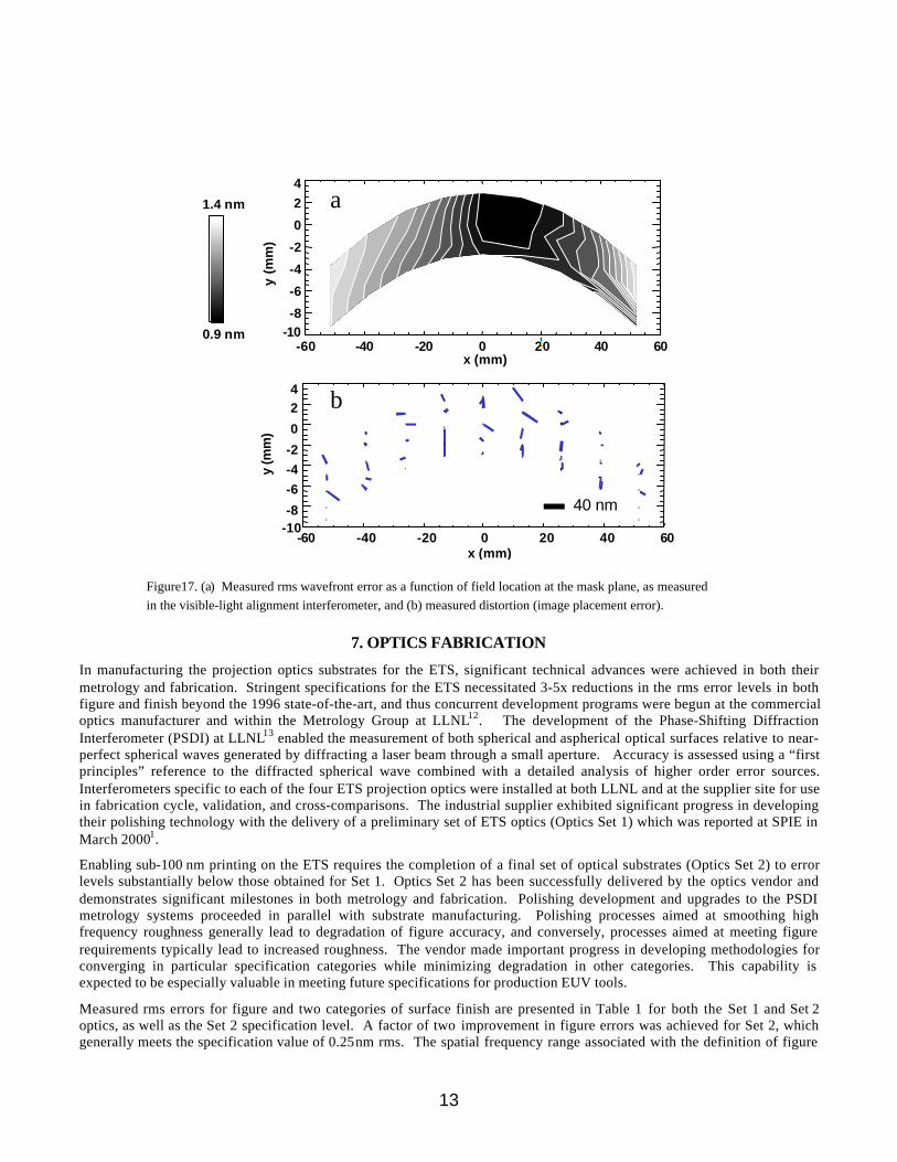
The final alignment results are shown in Figure 17, which displays a contour plot of the rms wavefront error (in the first 36Zernike polynomials) across the field and a vector plot of the image distortion. The wavefront error varies from 0.89 nm,near the center of the field, to 1.42 nm at the extremes of the field. The mean wavefront error is 1.20 nm. The meandistortion magnitude is 24 nm. However, the estimated error in the distortion measurement is 20 nm, indicating that, in termsof distortion, the alignment has converged to the measurement.
13
7. OPTICS FABRICATION
In manufacturing the projection optics substrates for the ETS, significant technical advances were achieved in both theirmetrology and fabrication. Stringent specifications for the ETS necessitated 3-5x reductions in the rms error levels in bothfigure and finish beyond the 1996 state-of-the-art, and thus concurrent development programs were begun at the commercialoptics manufacturer and within the Metrology Group at LLNL12. The development of the Phase-Shifting DiffractionInterferometer (PSDI) at LLNL13 enabled the measurement of both spherical and aspherical optical surfaces relative to near-perfect spherical waves generated by diffracting a laser beam through a small aperture. Accuracy is assessed using a “firstprinciples” reference to the diffracted spherical wave combined with a detailed analysis of higher order error sources.Interferometers specific to each of the four ETS projection optics were installed at both LLNL and at the supplier site for usein fabrication cycle, validation, and cross-comparisons. The industrial supplier exhibited significant progress in developingtheir polishing technology with the delivery of a preliminary set of ETS optics (Optics Set 1) which was reported at SPIE inMarch 20001.
Enabling sub-100 nm printing on the ETS requires the completion of a final set of optical substrates (Optics Set 2) to errorlevels substantially below those obtained for Set 1. Optics Set 2 has been successfully delivered by the optics vendor anddemonstrates significant milestones in both metrology and fabrication. Polishing development and upgrades to the PSDImetrology systems proceeded in parallel with substrate manufacturing. Polishing processes aimed at smoothing highfrequency roughness generally lead to degradation of figure accuracy, and conversely, processes aimed at meeting figurerequirements typically lead to increased roughness. The vendor made important progress in developing methodologies forconverging in particular specification categories while minimizing degradation in other categories. This capability isexpected to be especially valuable in meeting future specifications for production EUV tools.
Measured rms errors for figure and two categories of surface finish are presented in Table 1 for both the Set 1 and Set 2optics, as well as the Set 2 specification level. A factor of two improvement in figure errors was achieved for Set 2, whichgenerally meets the specification value of 0.25 nm rms. The spatial frequency range associated with the definition of figure
-60 -40 -20 0 20 40 60x (mm)
-10-8
-6
-4
-2
0
24
y (m
m)
0.9 nm
1.4 nm
-60 -40 -20 0 20 40 60x (mm)
-10-8
-6-4-2
0
24
y (m
m)
40 nm
a
b
Figure17. (a) Measured rms wavefront error as a function of field location at the mask plane, as measured in the visible-light alignment interferometer, and (b) measured distortion (image placement error).

14
includes all spatial wavelengths longer than 1 mm. A collage showingthe final surface figure measurements of Optics Set 2 made with thePSDI are shown in Figure 18. These particular measurements includecontributions from 1) long period errors that contribute to low-orderaberrations; 2) higher-order figure errors that are not significantlyaffected by alignment; and 3) waviness errors that contribute to flare.The category of finish labeled MSFR (Mid-Spatial FrequencyRoughness) includes spatial periods between 1 mm and 1 micron andleads to near-angle scattering. The improvement in MSFR and in thehigher frequency region of figure will lead to a substantial reduction inflare. Finally, the finish category labeled HSFR (High-SpatialFrequency Roughness) is defined for periods shorter than 1 micron andrelates to scattering outside of the optical system and generallyrepresents a throughput loss.
Two fabrication issues caused aspects of the Set 2 optics be slightlyout of specification. First, the surface of M2 deformed due to edgemachining performed after the final polishing operation, causing figureerror level to exceed the specification. Although, this type ofdeformation was anticipated, the magnitude was larger than expected.We hypothesize that residual stress in the bulk material “relaxed” aftermaterial in this area was removed. Although the vendor was preparedto make a figure correction, it was deemed unnecessary after detailedmodeling of the optical system showed that the error was almostentirely low order and could be compensated during alignment.
The HSFR for Set 2 exceeds the 0.10 n m rms specification by about afactor of 2x. The original specification value was set aggressively atthe beginning of the ETS contract to a level that is often obtained onsmall superpolished flats (Zerodur). However, during the course ofthe project, achieving this low level of HSFR has been elusive due tothe use of tooling appropriate for curved (aspheric) optics instead offlats. The HSFR levels are generally higher for Set 2, which is anindication of the coupling between the figuring and smoothingoperations. The tighter figure specification for Set 2 is achieved withsome trade-off from finish. The added roughness will lead toadditional throughput loss and be evident as a lower reflectance (1-2%)from the multilayer coating. Since delivering the Set 2 optics, thevendor has demonstrated the ability to attain lower levels of HSFR(~0.15 n m rms on M3). Another category not indicated in Table 1 is
the uniformity of roughness over the substrates, which could impact the uniformity of flare and throughput over the field, anduniformity of illumination over the pupil fill. The section on multilayer coating provides greater detail of this latter point,although the general area of uniformity is still being analyzed.
8. MULTILAYER COATINGS FOR SET 2 PROJECTION OPTICS
Set 2 of the four projection optics (M1, M2, M3, M4) for the ETS has been successfully coated and characterized. All fourmirrors were multilayer-coated with Mo/Si during a single deposition run using a new, production-scale DC-magnetronsputtering system (installed at LLNL), described in detail in Ref. 14. Coating simultaneously all optics insures bestwavelength matching and maximizes the throughput of the EUVL tool. During multilayer deposition, the Set 2 mirrors werespun around their optical axis and not around the center of their clear aperture, as was the case for the Set 1 optics15. Theadvantage of the Set 2 coating geometry is that all thickness errors are rotationally symmetric around the optical axis andaffect all field points in the same way, easing the task of compensating errors in the alignment of the ETS. On the otherhand, multilayer thickness has to be controlled to larger radii with the Set 2 coating arrangement, thus, achievement of thedesired uniform thickness profile becomes more challenging. Ideally, the multilayer coatings should not degrade the residualwavefront error of the imaging system design and should effectively become “invisible” to the optical performance. For theSet 2 optics, this requirement is equivalent to depositing multilayer coatings which would be uniform in the clear aperture
112 mm
Figure: 0.25M1M1
Figure: 0.35M2M2
156 mm
M4M4 Figure: 0.25
118 mm
Figure: 0.22M3M3
51 mm
-1.0 nm
0
1.0 nm
0.5
-0.5
Figure 18. Final figure measurements ofOptics Set 2 made using the PSDI. Substrateswere polished at SVG-Tinlsey (Richmond, CA)
Table 1. Measured and specified values for figureand finish for Optics Set 1 and Optics Set 2.
0.25 0.21 0.24
0.35 0.20 0.19
0.22 0.15 0.24
0.25 0.22 0.17
Figure:Figure: MSFR:MSFR: HSFR:HSFR:
Figure:Figure: MSFR:MSFR: HSFR:HSFR:
Figure:Figure: MSFR:MSFR: HSFR:HSFR:
Figure:Figure: MSFR:MSFR: HSFR:HSFR:
0.25 0.20 0.10
0.25 0.20 0.10
0.25 0.20 0.10
0.25 0.20 0.10
Set 1Set 1 Set 2Set 2 SpecSpec
0.40 0.30 0.14
0.45 0.25 0.16
0.38 0.26 0.17
0.49 0.28 0.17
M 1M 1
M 2M 2
M 3M 3
M 4M 4
(all units in nm rms)
15
region to within ±0.2% peak-to-valley (P-V) and add a figure error of less than 0.1 nm rms. (For comparison, therequirements for the Set 1 optics were ±0.25% P-V uniformity and 0.15 nm rms added figure error).
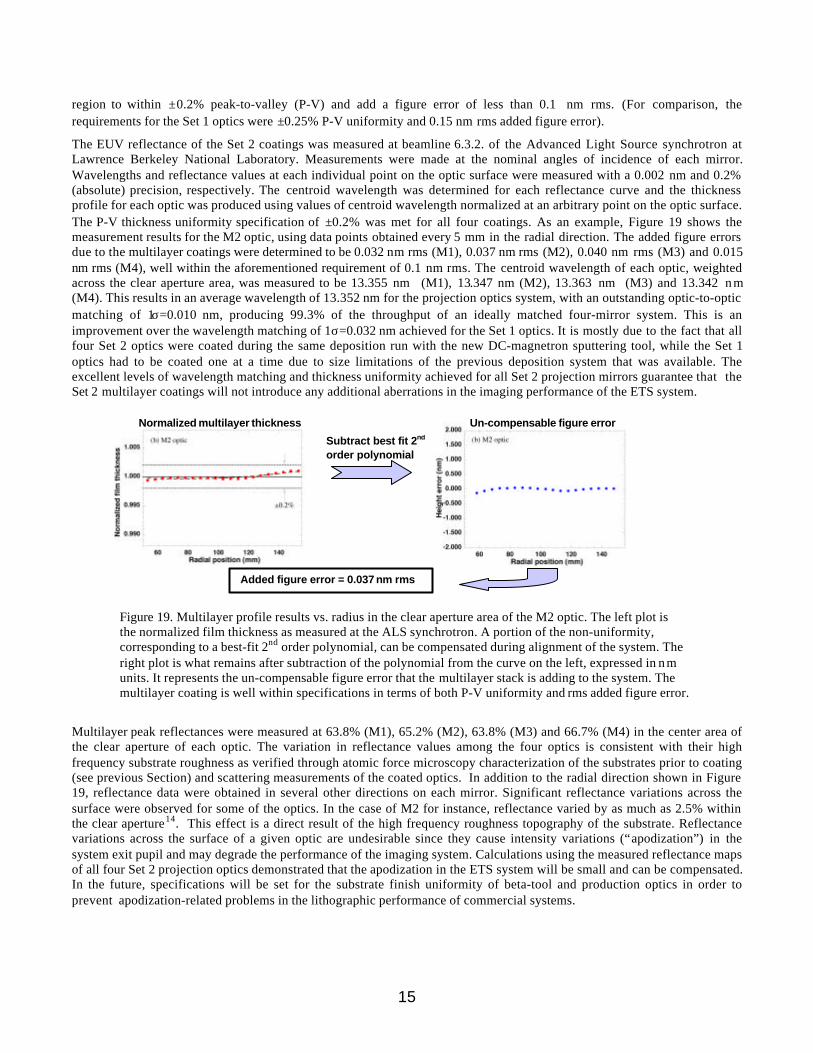
The EUV reflectance of the Set 2 coatings was measured at beamline 6.3.2. of the Advanced Light Source synchrotron atLawrence Berkeley National Laboratory. Measurements were made at the nominal angles of incidence of each mirror.Wavelengths and reflectance values at each individual point on the optic surface were measured with a 0.002 nm and 0.2%(absolute) precision, respectively. The centroid wavelength was determined for each reflectance curve and the thicknessprofile for each optic was produced using values of centroid wavelength normalized at an arbitrary point on the optic surface.The P-V thickness uniformity specification of ±0.2% was met for all four coatings. As an example, Figure 19 shows themeasurement results for the M2 optic, using data points obtained every 5 mm in the radial direction. The added figure errorsdue to the multilayer coatings were determined to be 0.032 nm rms (M1), 0.037 nm rms (M2), 0.040 nm rms (M3) and 0.015nm rms (M4), well within the aforementioned requirement of 0.1 nm rms. The centroid wavelength of each optic, weightedacross the clear aperture area, was measured to be 13.355 nm (M1), 13.347 nm (M2), 13.363 nm (M3) and 13.342 n m(M4). This results in an average wavelength of 13.352 nm for the projection optics system, with an outstanding optic-to-opticmatching of 1σ=0.010 nm, producing 99.3% of the throughput of an ideally matched four-mirror system. This is animprovement over the wavelength matching of 1σ=0.032 nm achieved for the Set 1 optics. It is mostly due to the fact that allfour Set 2 optics were coated during the same deposition run with the new DC-magnetron sputtering tool, while the Set 1optics had to be coated one at a time due to size limitations of the previous deposition system that was available. Theexcellent levels of wavelength matching and thickness uniformity achieved for all Set 2 projection mirrors guarantee that theSet 2 multilayer coatings will not introduce any additional aberrations in the imaging performance of the ETS system.
Figure 19. Multilayer profile results vs. radius in the clear aperture area of the M2 optic. The left plot isthe normalized film thickness as measured at the ALS synchrotron. A portion of the non-uniformity,corresponding to a best-fit 2nd order polynomial, can be compensated during alignment of the system. Theright plot is what remains after subtraction of the polynomial from the curve on the left, expressed in n munits. It represents the un-compensable figure error that the multilayer stack is adding to the system. Themultilayer coating is well within specifications in terms of both P-V uniformity and rms added figure error.
Multilayer peak reflectances were measured at 63.8% (M1), 65.2% (M2), 63.8% (M3) and 66.7% (M4) in the center area ofthe clear aperture of each optic. The variation in reflectance values among the four optics is consistent with their highfrequency substrate roughness as verified through atomic force microscopy characterization of the substrates prior to coating(see previous Section) and scattering measurements of the coated optics. In addition to the radial direction shown in Figure19, reflectance data were obtained in several other directions on each mirror. Significant reflectance variations across thesurface were observed for some of the optics. In the case of M2 for instance, reflectance varied by as much as 2.5% withinthe clear aperture14. This effect is a direct result of the high frequency roughness topography of the substrate. Reflectancevariations across the surface of a given optic are undesirable since they cause intensity variations (“apodization”) in thesystem exit pupil and may degrade the performance of the imaging system. Calculations using the measured reflectance mapsof all four Set 2 projection optics demonstrated that the apodization in the ETS system will be small and can be compensated.In the future, specifications will be set for the substrate finish uniformity of beta-tool and production optics in order toprevent apodization-related problems in the lithographic performance of commercial systems.
Added figure error = 0.037 nm rms
Subtract best fit 2nd
order polynomial
Normalized multilayer thickness Un-compensable figure error
16
9. INITIAL TOOL-SETUP RESULTS
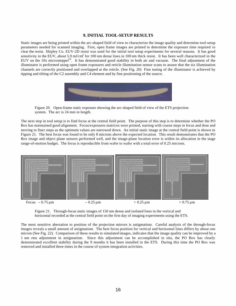
Static images are being printed within the arc-shaped field of view to characterize the image quality and determine tool-setupparameters needed for scanned imaging. First, open frame images are printed to determine the exposure time required toclear the resist. Shipley Co. EUV-2D resist was used for the initial tool setup experiments for several reasons. It has goodsensitivity in the EUV, about 5.9 mJ/cm2 for 100 nm dense lines in 100 nm thick resist. It has been well characterized in theEUV on the 10x microstepper16. It has demonstrated good stability in both air and vacuum. The final adjustment of theilluminator is performed using open frame exposures and reticle illumination sensor scans to assure that the six illuminationchannels are correctly positioned and overlapped at the reticle. (See Fig. 20) Fine tuning of the illuminator is achieved bytipping and tilting of the C2 assembly and C4 element and by fine positioning of the source.
Figure 20. Open-frame static exposure showing the arc-shaped field of view of the ETS projectionsystem. The arc is 24 mm in length.
The next step in tool setup is to find focus at the central field point. The purpose of this step is to determine whether the POBox has maintained good alignment. Focus/exposures matrices were printed, starting with coarse steps in focus and dose andmoving to finer steps as the optimum values are narrowed down. An initial static image at the central field point is shown inFigure 21. The best focus was found to be only 8 microns above the expected location. This result demonstrates that the POBox image and object plane sensors performed well, and the image-plane location error is within its allocation in the stagerange-of-motion budget. The focus is reproducible from wafer to wafer with a total error of 0.25 microns.
Focus – 0.75 µm – 0.25 µm + 0.25 µm + 0.75 µm
Figure 21. Through-focus static images of 150 nm dense and isolated lines in the vertical andhorizontal recorded at the central field point on the first day of imaging experiments using the ETS.
The most sensitive aberration to position of the projection mirrors is astigmatism. Careful analysis of the through-focusimages reveals a small amount of astigmatism. The best focus position for vertical and horizontal lines differs by about onemicron (See Fig. 22). Comparison of these results to simulated images, indicates that the image quality can be improved by a1 nm rms adjustment in astigmatism. Since this adjustment can be accomplished in situ, the PO Box has clearlydemonstrated excellent stability during the 9 months it has been installed in the ETS. During this time the PO Box wasremoved and installed three times in the course of system integration activities.
17
Focus – 0.75 µm – 0.25 µm + 0.25 µm + 0.75 µm
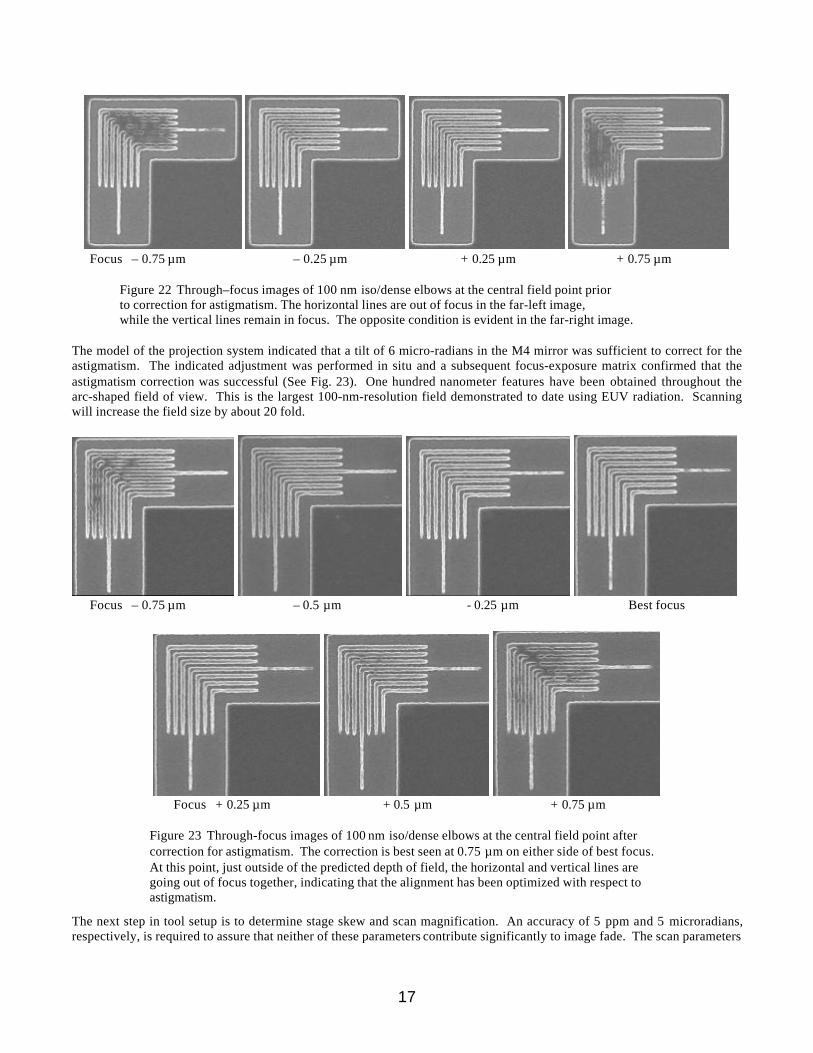
Figure 22 Through–focus images of 100 nm iso/dense elbows at the central field point priorto correction for astigmatism. The horizontal lines are out of focus in the far-left image,while the vertical lines remain in focus. The opposite condition is evident in the far-right image.
The model of the projection system indicated that a tilt of 6 micro-radians in the M4 mirror was sufficient to correct for theastigmatism. The indicated adjustment was performed in situ and a subsequent focus-exposure matrix confirmed that theastigmatism correction was successful (See Fig. 23). One hundred nanometer features have been obtained throughout thearc-shaped field of view. This is the largest 100-nm-resolution field demonstrated to date using EUV radiation. Scanningwill increase the field size by about 20 fold.
Focus – 0.75 µm – 0.5 µm - 0.25 µm Best focus
Focus + 0.25 µm + 0.5 µm + 0.75 µm
Figure 23 Through-focus images of 100 nm iso/dense elbows at the central field point aftercorrection for astigmatism. The correction is best seen at 0.75 µm on either side of best focus.At this point, just outside of the predicted depth of field, the horizontal and vertical lines aregoing out of focus together, indicating that the alignment has been optimized with respect toastigmatism.
The next step in tool setup is to determine stage skew and scan magnification. An accuracy of 5 ppm and 5 microradians,respectively, is required to assure that neither of these parameters contribute significantly to image fade. The scan parameters

18
are being determined by printing patterns of Leika IPRO marks and analyzing them using an IPRO tool. These experimentsare ongoing with the objective of demonstrating scanned images in the near future.
10. SUMMARY
The ETS is operational in static imaging mode, six months ahead of the originally planned operational date. The system isperforming as expected and in agreement with modeling results. One hundred nanometer isolated and dense features havebeen printed in the largest EUV print field demonstrated to date at this resolution. Stability of the projection system has beendemonstrated over a nine-month period during which it was installed three times in the course of system integration. Imagingperformance was improved by the correction of 1 nm rms astigmatism, through a small in situ adjustment of the projectionsystem, much the same as is done in advanced optical lithographic systems. Ongoing tool-setup experiments will determinethe machine parameters required to demonstrate scanned images in the near future.
These results have been achieved using a developmental projection system, while an improved projection system is beingassembled and aligned. The improved system uses a set of mirrors that has been fabricated to tighter tolerances and coatedwith multilayers to achieve nearly ideal wavelength matching. Upgrades in the other major subsystems are also underdevelopment. The source will be upgraded from 40 watts to 1700 watts of drive laser power and from a Xe gas-jet target to aXe liquid-jet target for improved conversion efficiency. The stage system will be upgraded from aluminum platens to low-thermal-expansion platens, and further stage modifications will enable scan speeds up to 10 mm/s at the wafer.
The performance goal for the ETS in its final configuration is to print 70 nm dense features in scanned images. During thecoming year the ETS will continue to deliver major new results in EUVL tool development as upgrades to the projectionoptics and other subsystems are completed.
ACKNOWLEDGMENTS
The authors are indebted to the members of the subsystem teams and technology teams, whose hard work is responsible foradvancing the EUV Engineering Test Stand to the state of development reported in this paper.
This work was performed by the University of California Lawrence Livermore National Laboratory under the auspices of theU.S. Department of Energy, Contract No. W-7405-ENG-48, by Sandia National Laboratories under the auspices of the U.S.Department of Energy, Contract No. DE-AC04-94AL85000, and by the Lawrence Berkeley National Laboratory under theauspices of the U.S. Department of Energy Office of Basic Energy Sciences. Funding was provided by the ExtremeUltraviolet Limited Liability Company under a Cooperative Research and Development Agreement.
REFERENCES1. D. A. Tichenor, G. D. Kubiak, W. C. Replogle, L. E. Klebanoff, J. B. Wronosky, L. C. Hale, H. N. Chapman, J. S.
Taylor, J. A. Folta, C. Montcalm, R. M. Hudyma, K. A. Goldberg, and P. Naulleau, “EUV Engineering Test Stand,”Emerging Lithographic Technologies IV, Proceeding of SPIE Vol. 3997, 48-69, (2000).
2. L. C. Hale, R. M. Hudyma, J. S. Taylor, R. L. Thigpen, and C. A. Jung, “High-NA Camera for an EUVL Microstepper,”Proceedings of the American Society for Precision Engineering, Vol. 22, 521-524 (2000).
3. K. A. Goldberg, P. Naulleau, P. J. Batson, P. Denham, E. H. Anderson, J. Bokor, and H. N. Chapman, “EUVInterferometry of a Four-Mirror Ring-field EUV Optical System,” Emerging Lithographic Technologies IV, Proceedingof SPIE Vol. 3997, 867-873, (2000).
4. L. E. Klebanoff, M. E. Malinowski, P. Grunow, W. M. Clift, C. Steinhaus, A. H. Leung, and S. J. Haney, “FirstEnvironmental Data from the EUV Engineering Test Stand,” these Proceedings.
5. G. D. Kubiak, L. J. Bernardez, K. Krenz, and W. C. Sweatt, “Scale-up of a Cluster Jet Laser Plasma Source for ExtremeUltraviolet Lithography”, Proceedings of the SPIE Vol. 3676, 669 (1999).
6. P. Celliers, L. B. Da Silva, C. B. Dane, S. Mrowka, M. Norton, J. Harder, L. Hackel, D. L. Matthews, H. Fiedorowicz,A. Bartnik, J. R. Maldonado, and J. A. Abate, “Optimization of X-ray Sources for Proximity Lithography Produced by aHigh Average Power Nd:glass Laser,” J. Appl. Phys. 79, 8258 (1996).
7. J. Blackburn, P. K. Carroll, J. Costello, and G. O’Sullivan, “Spectra of Xe VII, VIII, and IX in the Extreme Ultraviolet:4d-mp, nf Transitions,” J. Opt. Soc. Am. 73, 1325 (1983).
8. B. A. Hansson, M. Berglund, O. Hemberg. H. M. Hertz, “Xenon liquid-jet laser-plasma source for EUV lithography,”SPIE Conference on Microlithography, Santa Clara, CA, February (2001).
9. J. B. Wronosky, T. G. Smith, M. J. Craig, B. R. Sturgis , J. R. Darnold, D. K. Werling, M. A. Kincy, D. A. Tichenor, M.E. Williams, P. Bischoff, “Wafer and Reticle Positioning System for the Extreme Ultraviolet Lithography EngineeringTest Stand,” in Emerging Lithographic Technologies IV, Proceedings of SPIE Vol. 3997, 829-839 (2000).

19
10. K. A. Goldberg, P. Naulleau, P. J. Batson, P. Denham, E. H. Anderson, J. Bokor, and H. N. Chapman, “EUVInteferometry of a Four-Mirror Ring-Field EUV Optical System,” Emerging Lithographic Technologies IV, Proceedingof SPIE Vol. 3997, 867-873, (2000).
11. H. N. Chapman and D. W. Sweeney, “A Rigorous Method for Compensation Selection and Alignment ofMicrolithographic Optical Systems,” Proceedings of SPIE Vol. 3331, 102–113 (1998).
12. J. S. Taylor, G. E. Sommargren, D. W. Sweeney, and R. M. Hudyma, “The Fabrication and Testing of Optics for EUVProjection Lithography,” Emerging Lithographic Technologies II, Proceedings of SPIE Vol. 3331, pp. 580-590 (1998).
13. G. E. Sommargren, D. W. Phillion, E. W. Campbell, “Sub-nanometer interferometry for aspheric mirror fabrication,”from Precision Science and Technology for Perfect Surfaces, Proc. Of the 9th International Conference on PrecisionEngineering (9th ICPE), Aug. 29-Sep. 1, 1999, Osaka, Japan, JSPE Publication Series No. 3.
14. R. Soufli, E. Spiller, M. A. Schmidt, J. C. Davidson, R. F. Grabner, E. M. Gullikson, B. B. Kaufmann, S. L. Baker, H. N.Chapman, R. M. Hudyma, C. C. Walton, C. Montcalm, and J. A. Folta, “Multilayer optics for an extreme ultravioletlithography tool with 70 n m resolution,” this Conference Proceedings.
15. C. Montcalm, R. F. Grabner, R. M. Hudyma, M. A. Schmidt, E. Spiller, C. C. Walton, M. Wedowski, and J. A. Folta,“Multilayer coated optics for an alpha-class extreme ultraviolet lithography system,” in EUV, X-Ray, and Neutron Opticsand Sources, S. P. Vernon and K. Goldberg, Eds. Proceedings of SPIE Vol. 3767, 210-216 (1999).
16. R. L. Brainard, C. Henderson, J. Cobb, V. Rao, J. F. Mackevich, U. Okoroanyanwu, S. Gunn, J. Chambers, and S.Connolly, “Comparison of the Lithographic Properties of Positive Resists Upon Exposure to Deep- and Extreme-Ultraviolet Radiation,” 43rd International Conference on Electron, Ion, and Photon Beam Technology andNanofabrication , 3384-3389 (1999).