thiol–ene cross-linked polymer gate dielectrics for low-voltage organic thin-film transistors
TRANSCRIPT

Thiol−ene Cross-Linked Polymer Gate Dielectrics for Low-VoltageOrganic Thin-Film TransistorsChao Wang,† Wen-Ya Lee,† Reina Nakajima,† Jianguo Mei, Do Hwan Kim,‡ and Zhenan Bao*
Department of Chemical Engineering, Stanford University, Stanford, California 94305, United States
*S Supporting Information
ABSTRACT: We report a low-temperature processed, hydroxyl-free poly(vinyl phenyl) (PVP) dielectric layer cross-linked usingthiol−ene chemistry. This new dielectric material exhibited a high dielectric constant as compared to conventional hydroxyl-freepolymer dielectrics, e.g. polystyrene, and allowed for cross-linking at 80 °C, which is lower than the glass transition temperatureof most commonly used plastic substrates, e.g. poly(ethylene terathalate) (PET). Due to the absence of hydroxyl groups, thedielectric layer displayed more stable performance than other previously reported cross-linked PVP dielectrics. The low-temperature processing, high air stability, and low current−voltage hysteresis while retaining high device performances areimportant advantages of this new dielectric material.
KEYWORDS: organic thin-film transistors, polymer gate dielectrics, thiol−ene chemistry
Organic thin-film transistors (OTFTs) have attractedincreasing attention over the past two decades due to
their numerous advantages such as lightweight, inexpensivelarge area processing, and compatibility with flexible plasticsubstrates.1,2 While extensive research has been focused onsemiconductive materials to understand and improve theircharge transport properties,3,4 limited attention has beendevoted to the gate dielectric material. We believed thatdeveloping dielectric components possessing desirable proper-ties, e.g. stable performances, high throughput, and low-temperature solution-processing, will greatly benefit therealization of commercial electronics driven by organictransistors.5
For OTFTs, low-voltage transistor operation is of particularinterest for the development of portable electronics due to itslow power consumption, e.g. chemical detection in aqueousmedia.6 To achieve low-power applications, it is critical tomaintain a high output drain current (IDS), even in low voltageoperation. The magnitude of IDS is related to the applied gatevoltage (Vg) and the capacitance of the dielectric layers used inmost OTFTs. In general, the saturation IDS is defined by thefollow equation:2
μ= −I W L C V V/2 ( )iDS g th (1)
where W and L are channel width and length, respectively, Vththe threshold voltage, and Ci the capacitance per unit area ofthe dielectric layer. For identical device’s geometry andsemiconducting material, the increase in Ci allows obtainingthe equivalent output current in low-voltage operation. Ci canbe expressed by
ε=C k d/i 0 (2)
where ε0 is the vacuum permittivity, k is the dielectric constant,and d is the thickness of the insulator layer. Reducing thethickness is an efficient approach to obtain high current for low-voltage operation. However, thin dielectric films usually lead tohigh leakage current due to poor film uniformity and increasednumber of pin holes, causing low on−off current ratios. The useof ultrathin self-assembled nanodielectrics, such as self-assembled monolayer7,8 and multiple layers,9 is an alternativeway to enhance output current. However, obtaining high-quality film and full coverage of the self-assembly organic layersrequires precise processing controls and complex multipleprocesses. Increased capacitance of gate dielectricsis another
Received: September 30, 2013Revised: November 19, 2013Published: November 19, 2013
Article
pubs.acs.org/cm
© 2013 American Chemical Society 4806 dx.doi.org/10.1021/cm403203k | Chem. Mater. 2013, 25, 4806−4812

path to efficiently reduce driving voltage of OTFTs. The Frisbiegroup has demonstrated ion-gel dielectrics for low-voltage-driven OTFTs.10,11 Ion-gels consisting of a mobile ions within apolymer electrolyte provide ultra high capacitance exceeding 10μF cm−2. However, slow polarization and high leakage currentare still major challenges for the ion-gel gate dielectrics.Insulating polymers have been considered as a promising
material for gate dielectrics due to their solution processability.However, the operation of OTFTs made from polymerdielectrics generally require high voltages (>60 V), mainlyattributed to the resulting thick film (>300 nm) needed toreduce pin-holes and in obtaining low dielectric constant.Recently, a reduction in OTFT operating voltages has beenaccomplished by incorporating known insulator materials ordeveloping new systems based on cross-linkable polymers.12
For the latter, various cross-linked polymer systems have beenused for organic thin-film transistors, including polyimides,13
glass resins,14 poly(methyl methacrylate) (PMMA),15 poly-(vinyl alcohol),16 divinyltetramethyldisi loxane-bis-(benzocyclobutene) (BCB),17,18 polystyrene (PS),19 andphotoalignment layers.20
On the other hand, among the various polymer dielectrics,poly(4-vinylphenol) (PVP) based cross-linking systems areespecially attractive due to their high dielectric constant (∼4).Klauk et al. showed the first example of PVP-based dielectricsby mixing PVP with a cross-linking agent, poly(melamine-co-formaldehyde) (PMF), spin-coating the mixture from solution,and then curing at 180 °C.21 Yoon et al. have alsodemonstrated low-voltage OTFTs based on PVP films cross-linked with trichlorosilanes.22 Furthermore, we have alsoreported low-voltage OTFT operation by incorporatingultrathin films of poly(4-vinylphenol) cross-linked with 4,4′-(hexafluoroisopropylidene)diphthalic anhydride (HDA).23−26
These PVP-based dielectrics were observed to have gooddielectric properties, and the hydroxyl groups of PVP can bemodified by self-assembly monolayers (SAMs) to improvemolecular packing of organic semiconductors. A high holemobility of 1.2 cm2 V−1 s−1 was obtained on a SAM-modifiedPVP dielectrics when using pentacene as the semiconductor.22
Despite the observed high performances, PVP-based polymerdielectrics have some key limitations. One major limitation is itshigh curing temperature. The cross-linking of PVP is mostlyachieved via the formation of ester groups between the cross-linker and the hydroxyl groups on the polymer backbones. Thisreaction requires a high temperature process (usually >100 °C),which may distort the plastic substrate. The other majorlimitation is the high density of moisture-sensitive hydroxylgroups, since the unreacted free hydroxyl groups are remainedin the cross-linked PVP. The hydroxyl groups in the polymerare hydrophilic and can thus form hydrogen bonds with watermolecules. Therefore, PVP dielectrics are highly sensitive tomoisture in the air. The swelling effect of the PVP dielectrics iseven more severe when the devices are used in humidconditions or even under water. Besides, devices with PVPdielectrics usually show both large hysteresis and large leakagecurrent, since the hydroxyl groups may act as electron traps.Therefore, developing PVP-based polymer dielectrics that are(i) devoid of hydroxyl groups and (ii) cross-linked at lowtemperature is important for flexible polymer electronics.Recently, thiol−ene chemistry has emerged as a versatile and
efficient tool for cross-linking reaction, polymer functionaliza-tion, and surface modification.27−29 Herein, by introducingthiol−ene chemistry as a cross-linking approach, we have
successfully fabricated a low-temperature processing, hydroxyl-free PVP dielectric layer. This new dielectric layer exhibited ahigh dielectric constant as compared to conventional hydroxyl-free polymer dielectrics, e.g. polystyrene, and allowed for cross-linking at 80 °C, which is similar to, or even lower than, theglass transition temperature of most conventional plasticsubstrates, e.g. poly(ethylene terathalate) (PET) and polyimide.Due to the absence of hydroxyl groups, the dielectric layerdisplayed more stable performance than any other previouslyreported PVP−HDA dielectrics.
■ EXPERIMENTAL SECTIONMaterials. All materials were purchased from Sigma Aldrich and
used without further purification, unless otherwise noted. Propyleneglycol monomethyl ether acetate (PGMEA) was purchased from AlfaAesar. Poly(tetrathienoacene-diketopyrrolopyrrole) (PTDPPTFT4)was provided by Corning Incorporated,30 and the TIPS-pentacenewas provided by 3M.
Synthesis of PVP−Alkylene. Poly-4-vinylphenol (7.5 g, 50 mmol,MW = 25 000) was dissolved in a mixture solvent of acetone andtoluene (60 mL, V:V = 2:1), to which was added potassium carbonate(41.5 g, 300 mmol) and a phase transfer catalyst tetrabutylammoniumbromide (750 mg), followed by addition of allyl bromide (26 mL, 300mmol). The resulting mixture was refluxed for 10 h. Upon cooling toroom temperature, the solvent was evaporated. The precipitates werethen suspended into chloroform and passed through a pad of Celiteand silica gel and washed with chloroform (3 × 30 mL). The collectedchloroform solution was concentrated and precipitated into methanol.The white precipitates were collected and dried under vacuum at 60°C to give 9.1 g PVP−alkylene (96%, MW ∼ 33 000, dielectricconstant ∼ 4). H NMR (δ, CHCl3): 7.81−6.24 (m, 4H), 5.38−5.50(m, 1H), 5.36−5.20 (m, 1H), 4.62−4.38 (bs, 2H), 2.20−1.62 (m, 1H),1.60−1.18 (m, 2H).
Dielectric Film Preparation. PVP−alkylene, pentaerythritoltetra(3-mercapto propionate) (4T), and azobisisobutyronitrile(AIBN) were dissolved in PGMEA with concentrations of 40, 7.5,40 mg mL−1, respectively. The solutions were left for stirring overnightto obtain homogeneous solutions. The PVP-alkylene solution (2 mL)and AIBN solution (160 μL) were mixed together with 4T at variousratios (molar ratios between alkene groups and thiol groups are 1:1 (R= 1), 2:1 (R = 2), 4:1 (R = 4), and 8:1 (R = 8)) and vigorously stirredfor 3 min before being applied for spin-coating.
Highly doped silicon wafers were cut into small pieces (2.5 cm ×2.5 cm). The wafers were first cleaned with compressed air and washedwith toluene, acetone, and isopropanol, respectively. The cleaned Siwafers were then treated with UV-ozone for 20 min before spin-coating with dielectric polymers.
Spin-coating: 0.5 mL of the mixed solution was filtered through a0.2 μm syringe filter and dropped onto a piece of Si wafer. After 20 s, itwas spin-coated at a spin rate of 7000 rpm for 1 min. The as-preparedwafers were put on a hot-plate and cured at 80 °C in air for at least 3 h.The second layer of dielectrics was prepared with a similar procedure.The thickness of dielectrics, as measured by a profilometer, wasdetermined to be around 40−50 nm.
Dielectric Film of PVP−HDA Preparation. PVP−HDAdielectrics were prepared according to previous reports23 by mixing1 mL of poly-4-vinylphenol solution (40 mg/mL), 1 mL of HDAsolution (4 mg/mL), and 1 μL of triethylamine as a cross-linkingcatalyst. Two layers were deposited and cured at 110 °C for cross-linking at least 3 h. The thickness of obtained PVP−HDA doublelayers is about 45 nm.
Device Fabrication. A top-contact bottom-gate structure was usedfor our OTFTs. The polymer dielectrics were deposited on highlydoped silicon as described above. Four different organic semi-conductors were tested as a charge transport layer for OTFTs,respectively. Pentacene, 6,13-bis(triisopropylsilylethynyl)pentacene(TIPS-pentacene), and PTDPPTFT4 were used as p-channelmaterials, while hexadecafluorocopper phthalocyanine (F16CuPC)
Chemistry of Materials Article
dx.doi.org/10.1021/cm403203k | Chem. Mater. 2013, 25, 4806−48124807

was employed as an n-channel material. Pentacene and F-CuPc filmswere deposited by thermal evaporation (Angstrom Engineering) at arate of around 0.3 and 0.05−0.13 Å s−1 to thickness of 40 and 30 nm,respectively, under a pressure of 5.0 × 10⁻⁷ Torr. The substratetemperatures (Tsub) for pentacene and F-CuPc were controlled to be60 and 105 °C respectively by heating a copper block duringdeposition. PTDPPTFT4 was spin-coated at 1000 rpm for 60 s from a1,2,4-trichlorobenzene solution and then thermally annealed at 190 °Cfor an hour. TIPS-pentacene in toluene was deposited by ourpreviously reported solution-shearing method with a shearing speed of2.8 mm s−1 and substrate temperature at 90 °C. The gold electrodesfor source and drain electrodes were thermally evaporated at 0.5 Å s−1
to be 40 nm on a rotating substrate. Electrode dimensions weredefined by a shadow mask with a channel width (W) of 1 mm andchannel length (L) of 50 μm. The electrical measurements of OTFTswere carried out under ambient conditions or in an inert atmosphereby using a Keithley 4200-SCS semiconductor parameter analyzer(Keithley Instruments, Cleveland, OH).Characterization. Tapping-mode AFM images of the films was
recorded using a Multimode Nanoscope III with Extender electronics(Digital Instruments/Veeco Metrology Group, Santa Barbara, CA).The capacitance of the polymer dielectrics was measured with AgilentE4980A Precision LCR Meter for frequencies ranging from 20 Hz to10 kHz in ambient condition. Water stability was evaluated bycapacitance changes. A sandwich electrode structure with goldelectrodes (thickness 40 nm, gold area 0.0225 cm2) is soaked indeionized water in corresponding time, and then water residue isremoved from the surface using an air gun prior to measuringcapacitance. Contact angles were measured by using a goniometer(First Ten Angstroms FTA200) equipped with a CCD camera.
■ RESULTS AND DISCUSSION
Polymer Dielectrics PVP−4T. The design of our newdielectric layer was shown in Figure 1. The precursors of thedielectric layer were consisted of three components: PVP−alkene polymer, multithiol cross-linker, and radical initiator.PVP−alkene polymer was synthesized by converting thehydroxyl groups of PVP into alkene groups. NMR resultsshowed that nearly all the hydroxyl groups on PVP werereacted. We used pentaerythritol tetra(3-mercaptopropionate)(4T), a commercially available nonvolatile tetra-thiol as thecross-linker as it provides four reactive sites and can potentiallyresult in a more densely cross-linked network, which isdesirable for low leakage. AIBN, which can generate radicalswhen heated to over 70 °C, was chosen as radical initiator.These three components were dissolved and mixed in PGMEAand spin-coated onto a Si wafer into a thin film. The yielded
film was subsequently cured at 80 °C to obtain our desiredPVP−4T dielectrics.To investigate the optimized ratio between PVP−alkene
polymer and 4T cross-linkers, we prepared a series of PVP−4Tfilms of similar film thicknesses (at 40 nm) but with differentmolar ratios. We define R as the molar ratios between alkenegroups and thiol groups. The morphologies of the films withdifferent R values are shown in Figure 2. When R = 1 or 2, the
films were rough and exhibited many pin-holes. However, whenthe R value was >4, smooth PVP−4T films (i.e., without anypin-holes) were observed. The roughness of PVP−4T (R = 4)and PVP−4T (R = 8) were 0.31 and 0.35 nm, respectively.
Dielectric Characterizations. The dielectric characteristicsof the gate dielectric layer were evaluated by measuringcapacitance and leakage current. Capacitance is the amount ofcharges stored at a specific voltage. The capacitance is mainlydetermined by dielectric constant and thin-film thickness. Thecapacitance and leakage current were estimated in a metal−insulator−metal sandwich structure. A gold electrode with anarea of 0.0225 cm2 was thermally deposited on polymer thinfilms on a heavily doped Si substrate. To evaluate PVP−4Tdielectric characteristics, capacitance of PVP−4T with different
Figure 1. Chemical structures of the crosslinked PVP dielectric polymer based on thiol-ene chemistry.
Figure 2. AFM images of the morphologies of the PVP−4T dielectricswith molar ratios of (a) 1:1, (b) 2:1, (c) 4:1, and (d) 8:1.
Chemistry of Materials Article
dx.doi.org/10.1021/cm403203k | Chem. Mater. 2013, 25, 4806−48124808
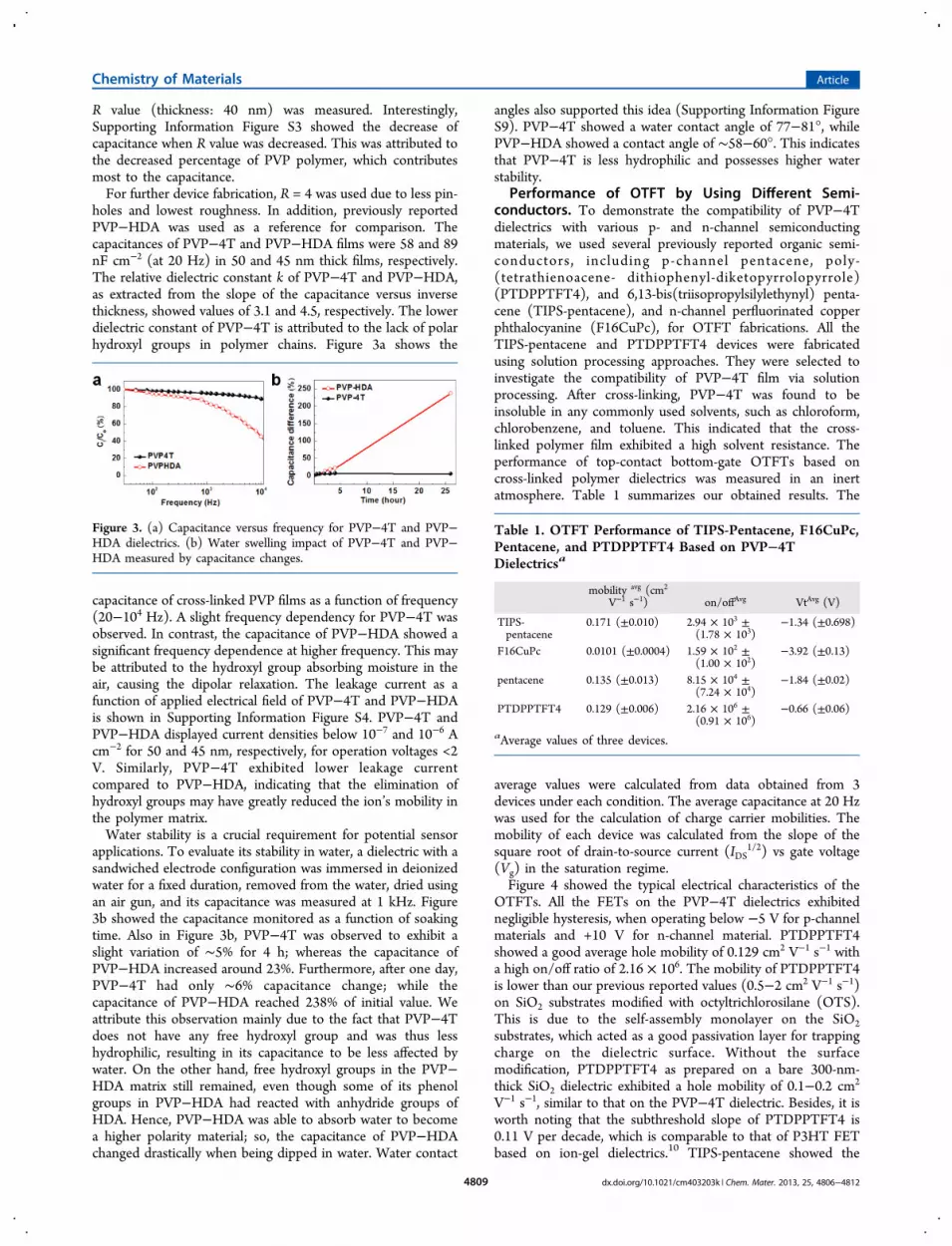
R value (thickness: 40 nm) was measured. Interestingly,Supporting Information Figure S3 showed the decrease ofcapacitance when R value was decreased. This was attributed tothe decreased percentage of PVP polymer, which contributesmost to the capacitance.For further device fabrication, R = 4 was used due to less pin-
holes and lowest roughness. In addition, previously reportedPVP−HDA was used as a reference for comparison. Thecapacitances of PVP−4T and PVP−HDA films were 58 and 89nF cm−2 (at 20 Hz) in 50 and 45 nm thick films, respectively.The relative dielectric constant k of PVP−4T and PVP−HDA,as extracted from the slope of the capacitance versus inversethickness, showed values of 3.1 and 4.5, respectively. The lowerdielectric constant of PVP−4T is attributed to the lack of polarhydroxyl groups in polymer chains. Figure 3a shows the
capacitance of cross-linked PVP films as a function of frequency(20−104 Hz). A slight frequency dependency for PVP−4T wasobserved. In contrast, the capacitance of PVP−HDA showed asignificant frequency dependence at higher frequency. This maybe attributed to the hydroxyl group absorbing moisture in theair, causing the dipolar relaxation. The leakage current as afunction of applied electrical field of PVP−4T and PVP−HDAis shown in Supporting Information Figure S4. PVP−4T andPVP−HDA displayed current densities below 10−7 and 10−6 Acm−2 for 50 and 45 nm, respectively, for operation voltages <2V. Similarly, PVP−4T exhibited lower leakage currentcompared to PVP−HDA, indicating that the elimination ofhydroxyl groups may have greatly reduced the ion’s mobility inthe polymer matrix.Water stability is a crucial requirement for potential sensor
applications. To evaluate its stability in water, a dielectric with asandwiched electrode configuration was immersed in deionizedwater for a fixed duration, removed from the water, dried usingan air gun, and its capacitance was measured at 1 kHz. Figure3b showed the capacitance monitored as a function of soakingtime. Also in Figure 3b, PVP−4T was observed to exhibit aslight variation of ∼5% for 4 h; whereas the capacitance ofPVP−HDA increased around 23%. Furthermore, after one day,PVP−4T had only ∼6% capacitance change; while thecapacitance of PVP−HDA reached 238% of initial value. Weattribute this observation mainly due to the fact that PVP−4Tdoes not have any free hydroxyl group and was thus lesshydrophilic, resulting in its capacitance to be less affected bywater. On the other hand, free hydroxyl groups in the PVP−HDA matrix still remained, even though some of its phenolgroups in PVP−HDA had reacted with anhydride groups ofHDA. Hence, PVP−HDA was able to absorb water to becomea higher polarity material; so, the capacitance of PVP−HDAchanged drastically when being dipped in water. Water contact
angles also supported this idea (Supporting Information FigureS9). PVP−4T showed a water contact angle of 77−81°, whilePVP−HDA showed a contact angle of ∼58−60°. This indicatesthat PVP−4T is less hydrophilic and possesses higher waterstability.
Performance of OTFT by Using Different Semi-conductors. To demonstrate the compatibility of PVP−4Tdielectrics with various p- and n-channel semiconductingmaterials, we used several previously reported organic semi-conductors, including p-channel pentacene, poly-(tetrathienoacene- dithiophenyl-diketopyrrolopyrrole)(PTDPPTFT4), and 6,13-bis(triisopropylsilylethynyl) penta-cene (TIPS-pentacene), and n-channel perfluorinated copperphthalocyanine (F16CuPc), for OTFT fabrications. All theTIPS-pentacene and PTDPPTFT4 devices were fabricatedusing solution processing approaches. They were selected toinvestigate the compatibility of PVP−4T film via solutionprocessing. After cross-linking, PVP−4T was found to beinsoluble in any commonly used solvents, such as chloroform,chlorobenzene, and toluene. This indicated that the cross-linked polymer film exhibited a high solvent resistance. Theperformance of top-contact bottom-gate OTFTs based oncross-linked polymer dielectrics was measured in an inertatmosphere. Table 1 summarizes our obtained results. The
average values were calculated from data obtained from 3devices under each condition. The average capacitance at 20 Hzwas used for the calculation of charge carrier mobilities. Themobility of each device was calculated from the slope of thesquare root of drain-to-source current (IDS
1/2) vs gate voltage(Vg) in the saturation regime.Figure 4 showed the typical electrical characteristics of the
OTFTs. All the FETs on the PVP−4T dielectrics exhibitednegligible hysteresis, when operating below −5 V for p-channelmaterials and +10 V for n-channel material. PTDPPTFT4showed a good average hole mobility of 0.129 cm2 V−1 s−1 witha high on/off ratio of 2.16 × 10⁶. The mobility of PTDPPTFT4is lower than our previous reported values (0.5−2 cm2 V−1 s−1)on SiO2 substrates modified with octyltrichlorosilane (OTS).This is due to the self-assembly monolayer on the SiO2substrates, which acted as a good passivation layer for trappingcharge on the dielectric surface. Without the surfacemodification, PTDPPTFT4 as prepared on a bare 300-nm-thick SiO2 dielectric exhibited a hole mobility of 0.1−0.2 cm2
V−1 s−1, similar to that on the PVP−4T dielectric. Besides, it isworth noting that the subthreshold slope of PTDPPTFT4 is0.11 V per decade, which is comparable to that of P3HT FETbased on ion-gel dielectrics.10 TIPS-pentacene showed the
Figure 3. (a) Capacitance versus frequency for PVP−4T and PVP−HDA dielectrics. (b) Water swelling impact of PVP−4T and PVP−HDA measured by capacitance changes.
Table 1. OTFT Performance of TIPS-Pentacene, F16CuPc,Pentacene, and PTDPPTFT4 Based on PVP−4TDielectricsa
mobility avg (cm2
V−1 s−1) on/offAvg VtAvg (V)
TIPS-pentacene
0.171 (±0.010) 2.94 × 10³ ±(1.78 × 10³)
−1.34 (±0.698)
F16CuPc 0.0101 (±0.0004) 1.59 × 10² ±(1.00 × 10²)
−3.92 (±0.13)
pentacene 0.135 (±0.013) 8.15 × 10⁴ ±(7.24 × 10⁴)
−1.84 (±0.02)
PTDPPTFT4 0.129 (±0.006) 2.16 × 10⁶ ±(0.91 × 10⁶)
−0.66 (±0.06)
aAverage values of three devices.
Chemistry of Materials Article
dx.doi.org/10.1021/cm403203k | Chem. Mater. 2013, 25, 4806−48124809

highest mobility of up to 0.171 cm2 V−1 s−1 with an on/off ratio2.94 × 103 and a subthreshold slope of 0.4 V per decade at agate bias of −5 V. This low on/off ratio may be attributed toimpurities embedded in unpurified TIPS-pentacene, causing ahigh leakage current. Additionally, we have also recentlyobserved aggregates from impurities of TIPS-pentacene insolution-processed films.31 The nature of these impurities inTIPS-pentacene is under investigation. As compared topreviously reported OTFTs based on cross-linked PVP-HDAdielectrics, our PVP−4T devices displayed a much smallerhysteresis. This is again attributed to the hydroxyl-free surfaceof cross-linked PVP−4T removing charge traps at the interfacebetween the semiconductors and dielectrics. Similarly, theelectron mobility (1.01 × 10⁻² cm2 V−1 s−1) of F16CuPcdevices, fabricated using the PVP−4T dielectrics, showedalmost 1 order of magnitude higher than our previouslyreported value (0.001−0.003 cm2 V−1 s−1) of F16CuPc25 usingPVP−HDA dielectrics. A reduction of n-channel behaviors inPVP−HDA is attributed to charge trapping of hydroxyl groups.To support this reasoning, Chua et al. have also reported thatelectron carriers can easily be trapped by electron-affinityhydroxyl groups to generate immobile negative ions, hencecompensating the applied external gate voltage.3,18 Thus, thehighly electron-affinity hydroxyl groups of PVP−HDA mayreduce the activity of n-type OTFTs. For the n-type OTFTs, ahydroxyl-free cross-linked gate dielectric, such as a divinylte-tramethylsiloxane-bis(benzocyclobutene) derivative (BCB), hasbeen widely used.18 However, the cross-linking temperatures ofBCB are as high as 240−290 °C, which may be inappropriateon flexible plastic substrates. Therefore, PVP−4T, which wereprepared in a much lower temperature, is an attractivealternative hydroxyl-free cross-linked dielectric for n-typeOTFTs.Air Stability. For practical applications, air stability of
OTFTs is a great concern due to oxygen and moisture trapping
charges, resulting in the degradation of OTFT electricalproperties. To evaluate air stability, OTFT devices fabricatedusing TIPS-pentacene were used, since TIPS-pentacene hadgood mobility and better air stability in the ambient conditioncompared with other molecules, e.g. pentacene. The air-stabilityinvestigation of the TIPS-pentacene-based OTFT, on bothcross-linked PVP−4T and PVP−HDA dielectrics, was moni-tored by measuring their mobility, on/off ratio, and thresholdvoltage as a function of time (Figures 5a−c and S3 (SupportingInformation)). The OTFT performances on both dielectricsexhibited good ambient stability. In addition, compared withOTFT performance in inert atmosphere, PVP−4T with TIPS-pentacene showed a better performance probably due tounintentionally oxygen doping, hence reducing the chargeinjection barrier between electrodes and semiconductors.
Figure 4. Electrical characteristics of OTFTs based on (a) PTDPPTFT4, (b) TIPS-pentacne, (c) pentacene, and (d) F-CuPc semiconductorsfabricated using the PVP−4T dielectrics.
Figure 5. OTFT performance changes of PVP−4T and PVP−HDAwith TIPS-pentacene as semiconductor when OTFT devices wereexposed in the ambient condition.
Chemistry of Materials Article
dx.doi.org/10.1021/cm403203k | Chem. Mater. 2013, 25, 4806−48124810

After exposure in the air for more than 1 week, The OTFTson the PVP−4T dielectric exhibited slight changes from 0.34 to0.24 cm2 V−1 s−1, on−off ratios from 1.1 × 10⁵ to 8.5 × 10⁴, andthreshold voltages from −0.54 to −0.65 V. This fluctuation maybe due to the changes in relative humidity in the ambientcondition, which has also been reported for other organicsemiconductors.32 (Humidity measurements = day 1 0:60%, 262%, 3 48%, 10 31%). As described above, since PVP−4Tdielectrics were not greatly affected by humidity, we thusattributed the fluctuation to the presence of TIPS-pentacene.Ambient oxygen and moisture have both been documented
to cause hysteresis during electrical characteristics of OTFTs.The hysteresis of OTFTs is evaluated by using ΔVth, thedifference between threshold voltages measured during theforward and backward scanning steps. When there is nohysteresis, ΔVth will be zero. We observed that the OTFT withPVP−HDA showed a larger hysteresis than the PVP−4Tdevices. Furthermore, the IDS − VG hysteresis of PVP−4Tbecame even smaller after 10 days, as compared to the initialobtained hysteresis (Figures 5d and S7 (Supporting Informa-tion)). In addition, even after 10 days, the IDS − VDS outputcurve of PVP−4T was unchanged and no leakage currentincreases were observed on the devices (Supporting Informa-tion Figure S6). On the other hand, PVP−HDA dielectrics(being affected more by water or humidity) are able to trapmore charges, and subsequently, result in a larger hysteresis andleakage current, as observed from the IDS − VDS output curve.
■ CONCLUSIONWe have developed a new dielectric polymer, derived via thiol−ene cross-linking chemistry, for low-voltage organic transistors.Compared to previously reported PVP dielectrics, our cross-linked polymer described herein has the advantages of low-temperature processing, high air stability, and small hysteresis,while retaining high device performances. This dielectricmaterial should be highly applicable for efforts towarddeveloping flexible electronics and underwater sensors.
■ ASSOCIATED CONTENT*S Supporting InformationXPS, stability test in the air, and contact angle results. Thismaterial is available free of charge via the Internet at http://pubs.acs.org.
■ AUTHOR INFORMATIONCorresponding Author*E-mail: [email protected] Address‡D.H.K.: Department of Organic Materials and Fiber Engineer-ing, Soongsil University, Seoul, 156-743, Korea.Author Contributions†C.W., W.-Y.L., R.N.: These authors contributed equally to thiswork.NotesThe authors declare no competing financial interest.
■ ACKNOWLEDGMENTSThis work was supported by Air Force Office of ScientificResearch (FA9550-12-1-0190). D.H.K. acknowledges financialsupport by a grant (Code No. 2011-0031628) from the Centerfor Advanced Soft Electronics under the Global Frontier
Research Program of the Ministry of Science, ICT and FuturePlanning, Korea.
■ REFERENCES(1) Dimitrakopoulos, C. D.; Malenfant, P. R. L. Adv. Mater. 2002, 14(2), 99−117.(2) Bao, Z.; Locklin, J. Organic field-effect transistors; CRC press: BocaRaton, FL, 2007.(3) Zaumseil, J.; Sirringhaus, H. Chem. Rev. 2007, 107 (4), 1296−1323.(4) Mei, J.; Diao, Y.; Appleton, A. L.; Fang, L.; Bao, Z. J. Am. Chem.Soc. 2013, 135 (18), 6724−6746.(5) Ponce Ortiz, R.; Facchetti, A.; Marks, T. J. Chem Rev 2010, 110(1), 205−39.(6) Klauk, H.; Zschieschang, U.; Pflaum, J.; Halik, M. Nature 2007,445 (7129), 745−8.(7) Halik, M.; Klauk, H.; Zschieschang, U.; Schmid, G.; Dehm, C.;Schutz, M.; Maisch, S.; Effenberger, F.; Brunnbauer, M.; Stellacci, F.Nature 2004, 431 (7011), 963−966.(8) Ju, S.; Lee, K.; Janes, D. B.; Yoon, M.-H.; Facchetti, A.; Marks, T.J. Nano Lett. 2005, 5 (11), 2281−2286.(9) Liu, J.; Hennek, J. W.; Buchholz, D. B.; Ha, Y.-g.; Xie, S.; Dravid,V. P.; Chang, R. P. H.; Facchetti, A.; Marks, T. J. Adv. Mater. 2011, 23(8), 992−997.(10) Yan, H.; Chen, Z.; Zheng, Y.; Newman, C.; Quinn, J. R.; Dotz,F.; Kastler, M.; Facchetti, A. Nature 2009, 457 (7230), 679−686.(11) Lee, K. H.; Kang, M. S.; Zhang, S.; Gu, Y.; Lodge, T. P.; Frisbie,C. D. Adv. Mater. 2012, 24 (32), 4457−4462.(12) Facchetti, A.; Yoon, M. H.; Marks, T. J. Adv. Mater. 2005, 17(14), 1705−1725.(13) Ahn, T.; Kim, J. W.; Choi, Y.; Yi, M. H. Org. Electron. 2008, 9(5), 711−720.(14) Huang, C.; West, J. E.; Katz, H. E. Adv. Funct. Mater. 2007, 17(1), 142−153.(15) Narayanan Unni, K. N.; Pandey, A. K.; Nunzi, J.-M. Chem. Phys.Lett. 2005, 407 (1−3), 95−99.(16) Jang, Y.; Kim, D. H.; Park, Y. D.; Cho, J. H.; Hwang, M.; Cho,K. Appl. Phys. Lett. 2006, 88 (7), 072101−072103.(17) Chua, L.-L.; Ho, P. K. H.; Sirringhaus, H.; Friend, R. H. Appl.Phys. Lett. 2004, 84 (17), 3400.(18) Chua, L.-L.; Zaumseil, J.; Chang, J.-F.; Ou, E. C. W.; Ho, P. K.H.; Sirringhaus, H.; Friend, R. H. Nature 2005, 434 (7030), 194−199.(19) Kim, C.; Facchetti, A.; Marks, T. J. Science 2007, 318 (5847),76−80.(20) Chou, W. Y.; Cheng, H. L. Adv. Funct. Mater. 2004, 14 (8),811−815.(21) Klauk, H.; Halik, M.; Zschieschang, U.; Schmid, G.; Radlik, W.;Weber, W. J. Appl. Phys. 2002, 92 (9), 5259−5263.(22) Yoon, M.-H.; Yan, H.; Facchetti, A.; Marks, T. J. J. Am. Chem.Soc. 2005, 127 (29), 10388−10395.(23) Roberts, M. E.; Mannsfeld, S. C. B.; Queralto,́ N.; Reese, C.;Locklin, J.; Knoll, W.; Bao, Z. Proc. Natl. Acad. Sci. 2008, 105 (34),12134−12139.(24) Kaf̈er, D.; He, M.; Li, J.; Pambianchi, M. S.; Feng, J.; Mauro, J.C.; Bao, Z. Adv. Funct. Mater. 2013, DOI: 10.1002/adfm.201202009.(25) Roberts, M. E.; Queralto,́ N. r.; Mannsfeld, S. C. B.; Reinecke, B.N.; Knoll, W.; Bao, Z. Chem. Mater. 2009, 21 (11), 2292−2299.(26) Roberts, M. E.; LeMieux, M. C.; Bao, Z. Acs Nano 2009, 3 (10),3287−3293.(27) Hoyle, C. E.; Bowman, C. N. Angew. Chem., Int. Ed. 2010, 49(9), 1540−1573.(28) Hoyle, C. E.; Lee, T. Y.; Roper, T. J. Polym. Sci. Part A: Polym.Chem. 2004, 42 (21), 5301−5338.(29) Campos, L. M.; Killops, K. L.; Sakai, R.; Paulusse, J. M. J.;Damiron, D.; Drockenmuller, E.; Messmore, B. W.; Hawker, C. J.Macromolecules 2008, 41 (19), 7063−7070.(30) Matthews, J. R.; Niu, W.; Tandia, A.; Wallace, A. L.; Hu, J.; Lee,W.-Y.; Giri, G.; Mannsfeld, S. C. B.; Xie, Y.; Cai, S.; Fong, H. H.; Bao,Z.; He, M. Chem. Mater. 2013, 25 (5), 782−789.
Chemistry of Materials Article
dx.doi.org/10.1021/cm403203k | Chem. Mater. 2013, 25, 4806−48124811

(31) Naab, B. D.; Himmelberger, S.; Diao, Y.; Vandewal, K.; Wei, P.;Lussem, B.; Salleo, A.; Bao, Z. Adv. Mater. 2013, n/a−n/a.(32) Li, D.; Borkent, E.-J.; Nortrup, R.; Moon, H.; Katz, H.; Bao, Z.Appl. Phys. Lett. 2005, 86 (4), 042105−3.
Chemistry of Materials Article
dx.doi.org/10.1021/cm403203k | Chem. Mater. 2013, 25, 4806−48124812