thermal modeling and control in mobile and server systems
TRANSCRIPT
THERMAL MODELING AND CONTROL IN
MOBILE AND SERVER SYSTEMS
by
Mohammad Javad Dousti
A Dissertation Presented to the
FACULTY OF THE USC GRADUATE SCHOOL
UNIVERSITY OF SOUTHERN CALIFORNIA
In Partial Fulfillment of the
Requirements for the Degree
DOCTOR OF PHILOSOPHY
(COMPUTER ENGINEERING)
December 2015
Copyright 2015 Mohammad Javad Dousti

To my mother and my father,
for their endless love.
ii
Acknowledgments
�� �� ��ّ���ٚ ٚ◌ٚ◌ٚ◌ٚ◌ٚ◌ٚ◌ٚ◌ٚ◌ٚ◌ٚ◌ٚ◌ٚ◌ٚ◌ٚ◌ٚ◌ٚ◌ٚ◌ٚ◌ٚ◌ٚ◌ٚ◌ٚ◌ٚ◌ٚ◌ٚ◌ٚ◌ٚ◌ٛ◌ٛ◌ٛ◌ٛ◌ٛ◌ٛ◌ٛ◌ٛ◌ٛ◌ٛ◌ٛ
� ��� ��� ����
�� ��� ��� ���� ��� ��
� �� �� � � �������� �� �� ���� ������� � �� � ��. ����� �� �� � �� ��
���� ������ ��� ّ��� ���
� �� �� �� � ��� �� ��ّ ��� ������� ��� � ؛ �� ���� ����
�� �� ������ � � � �� � �� ������
�� � ��. �� ���� ���
�
������ �� � �� ���� �� � ���� ��� � ��
���� � �����
�� � �� � ���
��*
I would like to express my sincere gratitude to my advisor Professor Massoud
Pedram for the continuous support of my Ph.D. study and related research, for his
patience, motivation, and immense knowledge. His guidance significantly helped
me during my Ph.D. research.
Besides my advisor, I would like to thank my dissertation and qualifying
exam committees, Professors Murali Annavaram, Sandeep Gupta, William G.J.
Halfond, Aiichiro Nakano, and Viktor Prasanna for their insightful comments and
encouragement.
* Taken from the renowned book Gulistan written by Sa’adi Shirazi in AD 1258.
iii
I thank Professor Antonio Petraglia from Federal University of Rio de Janeiro,
Brazil for his help on the development of thermoelectric generator models during
his sabbatical at USC.
My sincere thanks also goes to Professor Shahin Nazarian who has given me
very valuable advises during past five years. Moreover, I would like to thank
Diane Demetras, the Director of Student Affairs at the Department of Electrical
Engineering at USC for her kind help in streamlining the administrative part of
my graduate studies.
I would like to thank my fellow members at the System Power Optimization and
Regulation Technology (SPORT) Lab and its alumni for stimulating discussions,
sleepless nights we were working together before deadlines, and for all the fun we
had in the last five years.
Last but not least, I would like to thank my beloved family. My mother and my
father have supported me in every step of my life and have been with me whenever
I felt lonely and in need. Studying abroad is difficult and I could not finish it
without my parents’ spiritual support. I love them and will always remain indebted
for their favors. I would like to extend my last gratitude to my older brother for all
of his guidance during the past twenty seven years of my life. He patiently taught
me very first lessons in computer programming. Moreover, he significantly helped
me during my studies—from the elementary school till the end of Ph.D. study.
iv
Contents
Dedication ii
Acknowledgments iii
List of Tables viii
List of Figures x
Abstract xiv
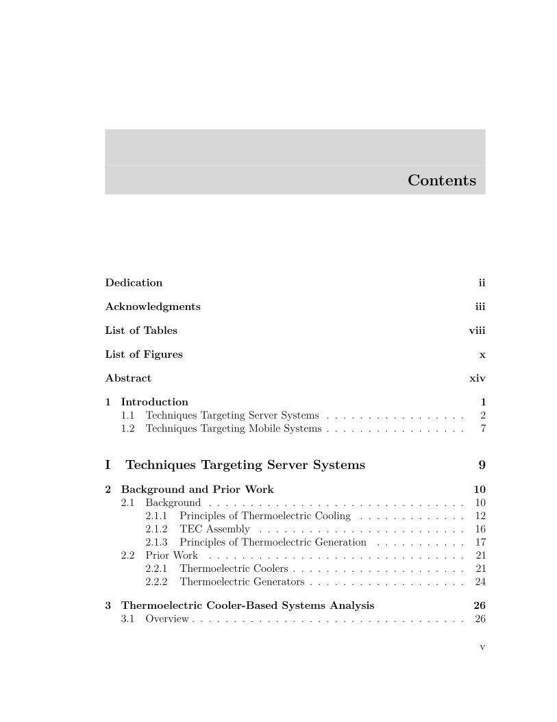
1 Introduction 11.1 Techniques Targeting Server Systems . . . . . . . . . . . . . . . . . 21.2 Techniques Targeting Mobile Systems . . . . . . . . . . . . . . . . . 7
I Techniques Targeting Server Systems 9
2 Background and Prior Work 102.1 Background . . . . . . . . . . . . . . . . . . . . . . . . . . . . . . . 10
2.1.1 Principles of Thermoelectric Cooling . . . . . . . . . . . . . 122.1.2 TEC Assembly . . . . . . . . . . . . . . . . . . . . . . . . . 162.1.3 Principles of Thermoelectric Generation . . . . . . . . . . . 17
2.2 Prior Work . . . . . . . . . . . . . . . . . . . . . . . . . . . . . . . 212.2.1 Thermoelectric Coolers . . . . . . . . . . . . . . . . . . . . . 212.2.2 Thermoelectric Generators . . . . . . . . . . . . . . . . . . . 24
3 Thermoelectric Cooler-Based Systems Analysis 263.1 Overview . . . . . . . . . . . . . . . . . . . . . . . . . . . . . . . . . 26
v
3.2 Redefining the COP . . . . . . . . . . . . . . . . . . . . . . . . . . 273.3 Platform-Dependent, Leakage-Aware Cooling Policy for TECs . . . 313.4 Experiments and Discussion . . . . . . . . . . . . . . . . . . . . . . 32
3.4.1 Simulation Setup . . . . . . . . . . . . . . . . . . . . . . . . 323.4.2 Simulation Results . . . . . . . . . . . . . . . . . . . . . . . 36
3.5 Summary . . . . . . . . . . . . . . . . . . . . . . . . . . . . . . . . 40
4 Joint Control of Forced-Convection and Thermoelectric Coolers 424.1 Overview . . . . . . . . . . . . . . . . . . . . . . . . . . . . . . . . . 424.2 Modeling . . . . . . . . . . . . . . . . . . . . . . . . . . . . . . . . . 444.3 Problem Formulation . . . . . . . . . . . . . . . . . . . . . . . . . . 48
4.3.1 Problem Statement . . . . . . . . . . . . . . . . . . . . . . . 484.3.2 Proposed Solution . . . . . . . . . . . . . . . . . . . . . . . 51
4.4 Experimental Results . . . . . . . . . . . . . . . . . . . . . . . . . . 534.4.1 Simulation Setup . . . . . . . . . . . . . . . . . . . . . . . . 534.4.2 Simulation Results . . . . . . . . . . . . . . . . . . . . . . . 56
4.5 Summary . . . . . . . . . . . . . . . . . . . . . . . . . . . . . . . . 61
5 Fine-Grained Control of Thermoelectric Coolers Using BypassSwitches 625.1 Overview . . . . . . . . . . . . . . . . . . . . . . . . . . . . . . . . . 625.2 Selective Control of TECs . . . . . . . . . . . . . . . . . . . . . . . 645.3 TEC Clustering . . . . . . . . . . . . . . . . . . . . . . . . . . . . . 67
5.3.1 Problem Formulation . . . . . . . . . . . . . . . . . . . . . . 675.3.2 Proposed Solution . . . . . . . . . . . . . . . . . . . . . . . 70
5.4 Experimental Results . . . . . . . . . . . . . . . . . . . . . . . . . . 735.4.1 Simulation Setup . . . . . . . . . . . . . . . . . . . . . . . . 735.4.2 Simulation Results . . . . . . . . . . . . . . . . . . . . . . . 74
5.5 Summary . . . . . . . . . . . . . . . . . . . . . . . . . . . . . . . . 77
6 Thermoelectric Generators Modeling 796.1 Overview . . . . . . . . . . . . . . . . . . . . . . . . . . . . . . . . . 796.2 Analytical Modeling of TEG Input Resistance . . . . . . . . . . . . 816.3 Sensitivity Analysis . . . . . . . . . . . . . . . . . . . . . . . . . . . 846.4 Maximum Power Point Tracking . . . . . . . . . . . . . . . . . . . . 866.5 Summary . . . . . . . . . . . . . . . . . . . . . . . . . . . . . . . . 89
II Techniques Targeting Mobile Systems 90
7 Background and Prior Work 917.1 Background . . . . . . . . . . . . . . . . . . . . . . . . . . . . . . . 91
vi
7.2 Prior Work . . . . . . . . . . . . . . . . . . . . . . . . . . . . . . . 957.2.1 Thermal Simulation . . . . . . . . . . . . . . . . . . . . . . . 957.2.2 Smartphone Power Characterization . . . . . . . . . . . . . 97
8 Therminator 2: A Fast Thermal Simulator 998.1 Overview . . . . . . . . . . . . . . . . . . . . . . . . . . . . . . . . . 998.2 Therminator 2 Architecture . . . . . . . . . . . . . . . . . . . . . . 1038.3 The Solver . . . . . . . . . . . . . . . . . . . . . . . . . . . . . . . . 104
8.3.1 Steady-State Analysis . . . . . . . . . . . . . . . . . . . . . 1058.3.1.1 LUP Decomposition . . . . . . . . . . . . . . . . . 1058.3.1.2 Cholesky Decomposition . . . . . . . . . . . . . . . 106
8.3.2 Transient Analysis . . . . . . . . . . . . . . . . . . . . . . . 1088.4 Implementation & Evaluation . . . . . . . . . . . . . . . . . . . . . 110
8.4.1 Implementation . . . . . . . . . . . . . . . . . . . . . . . . . 1108.4.2 Evaluation . . . . . . . . . . . . . . . . . . . . . . . . . . . . 111
8.4.2.1 Validation of Therminator 2 Results . . . . . . . . 1118.4.2.2 Convergence of Therminator 2 Results . . . . . . . 117
8.5 Case Study . . . . . . . . . . . . . . . . . . . . . . . . . . . . . . . 1188.6 Summary . . . . . . . . . . . . . . . . . . . . . . . . . . . . . . . . 123
9 ThermTap: A Power Analyzer and Thermal Simulator 1249.1 Overview . . . . . . . . . . . . . . . . . . . . . . . . . . . . . . . . . 1249.2 ThermTap Architecture . . . . . . . . . . . . . . . . . . . . . . . . 127
9.2.1 PowerTap: A Power Analyzer for Android Devices . . . . . . 1299.2.1.1 System State Monitor . . . . . . . . . . . . . . . . 1299.2.1.2 Power Profiler . . . . . . . . . . . . . . . . . . . . 131
9.2.2 Therminator 2: An Online Thermal Simulator . . . . . . . . 1369.2.3 ThermTap Implementation . . . . . . . . . . . . . . . . . . . 137
9.3 ThermTap Evaluation . . . . . . . . . . . . . . . . . . . . . . . . . 1379.4 Summary . . . . . . . . . . . . . . . . . . . . . . . . . . . . . . . . 140
10 Conclusion 142
Bibliography 145
vii
List of Tables
2.1 Comparison among different cooling techniques. . . . . . . . . . . . 11
2.2 Thermal quantities and their electrical duals. . . . . . . . . . . . . . 17
3.1 TEC parameters used in the simulations. . . . . . . . . . . . . . . . 34
3.2 Thermal resistivity, heat specific and dimensions of each layer of the
chip package. . . . . . . . . . . . . . . . . . . . . . . . . . . . . . . 35
4.1 Thermal conductivity and dimensions of various layers in the chip
package. . . . . . . . . . . . . . . . . . . . . . . . . . . . . . . . . . 55
4.2 Results of OFTEC for MiBench benchmarks. . . . . . . . . . . . . . 61
6.1 Kryotherm TB-127-1.4-1.2 parameters. . . . . . . . . . . . . . . . . 84
8.1 Temperatures obtained from the thermocouple measurement (TCM),
Autodesk Simulation CFD, and Therminator 2. Note the AP junction
temperature is read from temperature register (Reg) instead of
measurement. The ambient temperature is 23.0 ∘C. . . . . . . . . . 115
viii
8.2 Skin temperature and AP junction temperature obtained by ther-
mocouple measurement (TCM) and Therminator 2 at different AP
power consumption levels. . . . . . . . . . . . . . . . . . . . . . . . 120
ix
List of Figures
2.1 A 3×3 array of TECs. . . . . . . . . . . . . . . . . . . . . . . . . . 13
2.2 A TEC N-P pair. The aspect ratio of elements is not accurate and
sizes are exaggerated. The dashed arrow shows the direction of
current flow. . . . . . . . . . . . . . . . . . . . . . . . . . . . . . . . 15
2.3 A chip assembly with its cooling solution . . . . . . . . . . . . . . . 17
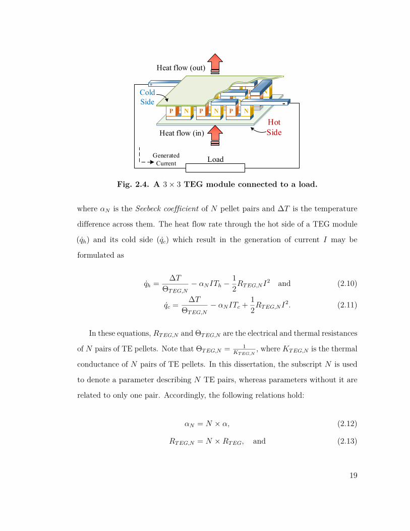
2.4 A 3× 3 TEG module connected to a load. . . . . . . . . . . . . . . 19
2.5 Electrothermal model of 𝑁 TEGs considering the contact thermal
resistances. The thermal part is represented in red and the electrical
part is shown in blue. . . . . . . . . . . . . . . . . . . . . . . . . . . 20
3.1 Dependency of 𝐶𝑂𝑃 𝑏𝑎𝑠𝑖𝑐𝑚𝑎𝑥 on Δ𝑇 , 𝑍𝑇𝑎𝑣𝑔, and 𝑇𝑐. . . . . . . . . . . . 29
3.2 An electrical model for a TEC embedded inside a processor package. 30
3.3 Curve fitting for the leakage power density of a Xeon processor in
32 nm process technology. . . . . . . . . . . . . . . . . . . . . . . . 35
x
3.4 Results of steady-state experiments with TECs. (a) Hot spot tem-
perature, (b) COP𝑠𝑦𝑠 values, (c) leakage power, and (d) absorbed
heat per unit time by all TECs for different current values ranging
from 0 A to 11 A. . . . . . . . . . . . . . . . . . . . . . . . . . . . . 38
3.5 Results of transient cooling experiments with TECs. (a) Hot spot
temperature change and (b) COP𝑠𝑦𝑠 change when applying a one-
second heat pulse to the center of the chip to make a hot spot. . . . 40
4.1 A sub-component in 𝐿𝑐𝑜𝑛𝑑𝑢𝑐𝑡 modeled by six resistors. . . . . . . . . 45
4.2 An electrical model for a TEC used in Teculator. . . . . . . . . . . 47
4.3 Dependence of the thermal conductance of combined heat sink and
fan on the fan rotation speed. . . . . . . . . . . . . . . . . . . . . . 48
4.4 The evaluation flow for OFTEC. . . . . . . . . . . . . . . . . . . . . 54
4.5 Maximum Die Temperature for Various 𝜔 and 𝐼𝑇 𝐸𝐶 Power. . . . . . 57
4.6 Cooling Power Consumption for Various 𝜔 and 𝐼𝑇 𝐸𝐶 Power. . . . . 57
4.7 Maximum chip temperature after Optimization 4.2. . . . . . . . . . 59
4.8 Cooling power after Optimization 4.2. . . . . . . . . . . . . . . . . . 59
4.9 Maximum chip temperature after Optimization 4.1. . . . . . . . . . 60
4.10 Cooling power after Optimization 4.1. . . . . . . . . . . . . . . . . . 60
5.1 The proposed circuit for selective control of TEC clusters. . . . . . 66
5.2 A set of intervals drawn for PARSEC benchmarks executed on Xeon
X5550. . . . . . . . . . . . . . . . . . . . . . . . . . . . . . . . . . . 75
5.3 The power saving percentage achieved by clustering TECs using the
proposed heuristic. . . . . . . . . . . . . . . . . . . . . . . . . . . . 76
5.4 Power waste break down. . . . . . . . . . . . . . . . . . . . . . . . . 76
5.5 Sensitivity analysis of power saving with respect to 𝑅𝐷𝑆,𝑜𝑛. . . . . . 77
xi
6.1 High-level structure of a TEG harvesting system. . . . . . . . . . . 81
6.2 Sensitivity analysis of resistance mismatch ratio on the Seebeck
coefficient. . . . . . . . . . . . . . . . . . . . . . . . . . . . . . . . . 85
6.3 Sensitivity analysis of resistance mismatch ratio on the TEG contact
and supper-lattice thermal resistivity. . . . . . . . . . . . . . . . . . 86
6.4 Sensitivity analysis of resistance mismatch ratio on the hot and cold
site temperatures of a TEG module. . . . . . . . . . . . . . . . . . . 87
6.5 Harvested power as a function of current drawn for various values of
Δ𝑇 and 𝑇𝑐. . . . . . . . . . . . . . . . . . . . . . . . . . . . . . . . 88
7.1 A cross-section view of the thermal RC network in a simple smart-
phone model. . . . . . . . . . . . . . . . . . . . . . . . . . . . . . . 93
8.1 Estimated exposure time of the human skin to the hot water in order
to result in a burn. . . . . . . . . . . . . . . . . . . . . . . . . . . . 100
8.2 Architecture of Therminator 2. . . . . . . . . . . . . . . . . . . . . 104
8.3 Comparison of the runtime of various implementation of the LUP
decomposition method for different sub-component counts. . . . . . 106
8.4 Runtime comparison between Therminator and Therminator 2 for
different number of components. . . . . . . . . . . . . . . . . . . . . 109
8.5 (a) Teardown of MSM8660 MDP device and temperature measure-
ment kits (circle marks are temperature measurement points. Note
for the PCB, thermocouple is attached onto the other side), (b) CFD
drawing, and (c) Therminator 2 3D visualization. . . . . . . . . . . 112
8.6 (a1, b1, c1) Temperature maps produced by Autodesk Simula-
tion CFD and (a2, b2, c2) by Therminator 2 for (a) the screen
protector, (b) rear case, and (c) PCB for the StabilityTest use case. 116
xii
8.7 Comparison of measured and simulated temperatures. . . . . . . . . 117
8.8 Therminator 2 results convergence and runtime versus sub-
component counts for the StabilityTest use case. . . . . . . . . . . . 118
8.9 3D layout for Samsung Galaxy S4. Sub-components are not shown. 119
8.10 AP power consumption and junction temperature versus various skin
temperature setpoints. . . . . . . . . . . . . . . . . . . . . . . . . . 121
8.11 (a) Skin and AP junction temperature versus rear case material and
(b) thermal pad material for 𝑃𝐴𝑃 =2.2 W. . . . . . . . . . . . . . . 122
9.1 ThermTap structure. On the left, the work flow of PowerTap and
its interaction with Android OS is shown. On the right, a simplified
work flow of Therminator 2 is depicted. The user should provide a
device physical specification along with the application/process that
he is interested in for probing. ThermTap generates temperature
maps of the selected application/process. . . . . . . . . . . . . . . . 128
9.2 SystemTap work flow. . . . . . . . . . . . . . . . . . . . . . . . . . 130
9.3 Power consumption of each core in the Nexus 5 drawn with respect
to the total number of active cores. . . . . . . . . . . . . . . . . . . 133
9.4 Comparing the power trace generated by PowerTap with measured
values. . . . . . . . . . . . . . . . . . . . . . . . . . . . . . . . . . . 138
9.5 ThermTap results while running QQPlayer (a) showing the entire
system and (b) showing only the impact of the player process. . . . 139
9.6 ThermTap results while running VLC (a) showing the entire system
and (b) showing only the impact of the player process. . . . . . . . 140
xiii
Abstract
This dissertation deals with thermal modeling and control issues in two types
of systems: servers and mobile devices. For server systems, thermoelectric coolers
(TECs) are considered as the cooling solution. Despite their unique benefits, TECs
generate heat during their operation due to the Joule heating effect. This reduces
their cooling efficiency and necessitates careful design and control in order to enable
their effective utilization. In this dissertation, three key issues are identified and
addressed. First, it is noted that the traditional definition of TEC coefficient of
performance (COP) is not useful for electronic cooling packages due to strong
dependence of the circuit leakage power on the die temperature. Hence, the COP
is redefined to consider the effect of leakage power. Second, it is found that in
a cooling package comprised of a fan and TECs, the TECs driving current and
fan rotation speed should be properly set to avoid power losses. Accordingly,
two optimization problems are set up and solved: One that tries to minimize the
maximum die temperature and another that aims to minimize the cooling power
consumption subject to the temperature constraint. Last, it is observed that hot
spots are spatially and temporally distributed on the surface of a chip. As a result,
conventional control of all TECs as a single unit is too coarse-grained and tends to
xiv
result in power inefficiencies. To address this issue, TECs are divided into a set of
clusters, where each cluster is instrumented with a bypass switch. The presence of
these switches enables a controller to selectively turn on and off each TEC cluster,
thereby, significantly enhancing the power efficiency of the TEC-based cooling
solution. For mobile devices, a tool called ThermTap is introduced to enable system
and software developers find power and thermal bugs in the design. ThermTap
comprises of a power analyzer called PowerTap and an online thermal simulator
called Therminator 2. Equipped with accurate power macro-models and utilizing
operating system kernel device drivers, PowerTap collects the activity profiles of
major components of a portable device in an event-driven manner, which are in
turn analyzed to produce power dissipation profiles (i.e., power traces) for these
components. Therminator 2 subsequently reads these traces and, using a compact
thermal model of the device, generates various temperature maps including those
for the device skin and the aforesaid components. Accurate per-process and per-
application temperature maps produced by ThermTap enable software and system
developers to find thermal bugs in their software.
xv
1Introduction
The successful continuation of Moore’s law depends on the continuous supply
voltage reduction. This reduction has been slowed down in the past few years.
More precisely, the voltage scaling for 32 nm and 22 nm technology nodes was
0.925x and 0.95x, respectively. It is estimated that for 14 nm and 10 nm process
technologies, the voltage scaling will be further slowed down to only 0.975x and
0.985x, respectively [1]. This trend reduces the power scaling for future generations
of IC chips, which consequently results in higher die power density.
High power density causes hot spots on the chip, which tends to accelerate the
device and interconnect aging processes and may even cause permanent physical
defects if the temperature of these hot spots exceeds a certain threshold [2]. Addi-
tionally, increased die temperatures result in slower devices and higher leakage
power dissipation. Furthermore, with ever increasing popularity of portable devices,
skin temperature has become an important constraint. As a result, thermal issue is
one of the main barriers to the successful continuation of Moore’s law. The purpose
of a thermal management system is to stop the temperature increase beyond a
certain threshold, even if the required action is to power off the chip. The remainder
of this chapter enumerates contributions of this dissertation in thermal modeling
and control techniques targeting server and mobile systems.
1
1.1 Techniques Targeting Server Systems
Various thermal management solutions have been proposed during the past
decade (e.g., [2], [3], [4], [5], [6], [7], [8], [9], [10], and [11]). These solutions tend
to negatively impact the chip performance. One solution that does not degrade
the performance is the use of advanced cooling materials and technologies. A
common disadvantage of various cooling techniques is their low heat-pumping
capability. In particular, none of the traditional techniques (i.e., active and passive
cooling methods) has the ability to pump heat fluxes higher than 1,000 W/cm2 [12].
Note also that active cooling methods, which have higher performance but require
external power supply, suffer from reliability issues and some of them, which provide
a relatively high heat pumping capability (e.g., the direct jet impingement method),
cannot be incorporated inside the chip package because of their large size. A new
active cooling method called thermoelectric cooling has recently caught attention
especially for cooling high-end multi-core processor chips [12].
Thermoelectric coolers (TECs) are active devices that work based on the Peltier
effect. This effect allows them to absorb heat from one side and release it to the
other side when electrical current passes through TECs. The amount of cooling is
linearly proportional to the amount of driving current. Notable features of TECs
are the following:
1. Compact size: TECs can be built as thin as tens of micrometers and
their area can be smaller than 1 mm2. These devices have the right size to
exclusively cover typical hot spots on a chip [13].
2. Fast response time: Thin-film TECs have very fast response time in the
order of a few milliseconds [14].
2
3. High reliability: These devices have no moving parts, and hence, they
can last longer than other active cooling solutions. Commercial TECs are
expected to work for more than 11 years [14].
4. High controllability: TECs can be controlled at the granularity of fractions
of a degree of Celsius and can cool down a chip below the ambient temperature
[14].
5. Very high heat pumping rate: It has been shown that thin-film TECs
can pump high heat fluxes as large as ∼1,300 W/cm2 [13].
Unique features of TECs make them a perfect candidate for cooling a chip.
Unfortunately, Joule heating occurs as an adverse phenomenon during the cooling
process by TECs, which causes them to dissipate heat when current flows through
them. Both the heat rejected from the hot spot and the heat generated by TECs
(as a result of Joule heating) must thus be disposed to the ambient; otherwise,
the accumulated heat on the hot side of TECs adversely affects their cooling
performance.
I identify three important issues that have to be addressed for effectively using
TECs inside a cooling package. In all of these issues, I carefully consider the strong
dependence of chip leakage power on the temperature. This is a key difference
between employing TECs for cooling electronic devices and using them in other
cooling applications. As a preliminary step, I develop a TEC simulator called
Teculator [15] which lets me perform thermal simulations and validate my models
and formulations.
First, it is noted that the traditional definition of TEC coefficient of performance
(COP) is not useful for electronic cooling packages due to strong dependence of
the circuit leakage power on the die temperature [15]. The COP is defined as
3
the ratio of the removed heat rate (i.e., cooling rate) to the power needed to
drive TECs. It is a good metric for selecting an appropriate cooling system for
a specific application. However, I observe that this definition is inadequate for
cooling electronic components due to the dependence of circuit leakage power on the
temperature. Hence, I formulate the COP for the cooling package of an electronic
system as
𝐶𝑂𝑃 𝑠𝑦𝑠 = 𝑞𝑐 − 𝑃𝑙𝑒𝑎𝑘𝑎𝑔𝑒
𝑃𝑇 𝐸𝐶,𝑁 + 𝑃𝑙𝑒𝑎𝑘𝑎𝑔𝑒
, (1.1)
where 𝑞𝑐 is the TEC heat removal rate, 𝑃𝑙𝑒𝑎𝑘𝑎𝑔𝑒 is the chip leakage power and
𝑃𝑇 𝐸𝐶,𝑁 is the power consumption of 𝑁 TECs integrated inside the cooling package.
Based on this new formulation, I propose a new compact thermal model for TECs
which considers the leakage power. One can use this model for the actual design of
a cooling package and also makes sure that the driving current of TECs is always
set such that 𝐶𝑂𝑃 𝑠𝑦𝑠 is maximized.
Next, it is found that in a cooling package comprised of a fan and TECs, the
TECs driving current and fan rotation speed should be properly set to avoid power
losses [16]. Using the forced-convection cooling along with TECs allows more heat
to be pumped from the chip using a fan. This extra ability comes at the cost
of increased cooling power consumption. In this case, the total cooling power
of the chip will be equal to the power usage of TECs and the fan. Moreover,
simultaneously controlling the fan and TECs such that the entire system meets its
thermal and power constraints is a challenging task. If TECs are driven by a high
current level and the fan rotation speed is set to be too low, the rejected heat is
trapped between the TEC and the fan, and hence, the hybrid cooling approach will
not be effective. On the other hand, if the driving current of TECs is set to be too
low but the fan rotation speed is set to be high, there is not enough pumped heat
for the fan to blow away. Moreoever, setting the fan speed and the TEC driving
4
current to high levels increases the cooling power consumption, which negatively
affects the power efficiency.
Based on the argument presented in the previous paragraph, I consider two
optimization problems: the minimization of the maximum die temperature and
the cooling power minimization subject to temperature constraints [16]. The die
temperature minimization problem is important when the power consumption of
the cooling system is less important compared to the negative effects of high die
temperature as explained earlier. On the other hand, the power minimization
problem is critical in power-aware applications. In these optimization problems,
the strong dependence of leakage power on the temperature is also considered.
Investing more power in the cooling may pay off well as a result of a dramatic
power saving in the chip leakage power consumption. Next, I find a high-quality
solution to the above optimization problems and develop a fast framework called
OFTEC (optimization of forced-convection and thermoelectric coolers) based on it.
Last, it is observed that the spatial and temporal distributions of hot spots on
the surface of a chip are non-uniform. As a result, conventional control of all TECs
as a single unit is too coarse-grained and tends to result in power inefficiencies. To
address this issue, I suggest that adjacent hot spots with the same thermal behavior
can be grouped and controlled by a cluster of TECs [17]. A bypass switch for each
TEC cluster is added in order to allow selectively turning off some TEC clusters
which are not needed. More precisely, a clustering problem is formulated and solved
which aims to minimize the power waste due to the excessive use of TECs. Based
on my experiments, I expect that the proposed technique can significantly reduces
the cooling power consumption.
I also briefly study Thermoelectric generators (TEGs) [18]. TEGs work based
on the Seebeck effect (the dual of the Peltier effect)—a temperature gradient across
5
TEGs produces a voltage difference over its terminals. TEGs provide a unique way
for harvesting thermal energy. Similar to TECs, these devices are compact, durable,
inexpensive, and scalable. Unfortunately, the conversion efficiency of TEGs is low.
This requires careful design of energy harvesting systems including the interface
circuitry between the TEG module and the load, with the purpose of minimizing
power losses. I analytically show that the traditional approach for estimating the
internal resistance of TEGs may result in a significant loss of harvested power.
This drawback comes from ignoring the dependence of the electrical behavior of
TEGs on their thermal behavior. Accordingly, a systematic method for accurately
determining the TEG input resistance is proposed. Based on this method, a
maximum power point tracking algorithm for TEGs is presented which only utilizes
temperature sensors’ data in order to adjust the interface circuitry. A tracking
method is necessary to offset the effect of temperature change across TEG junctions
on TEGs’ input resistance.
The first part of this dissertation is organized as follows. Chapter 2 overviews
the principals of thermoelectric cooling and generation plus the related work. Next,
Chapter 3 presents the solution to the first key issue (i.e., redefinition of the COP)
in detail. After that, Chapter 4 discusses OFTEC as the solution to the second
issue. Then, Chapter 5 explains the solution to the third key issue, i.e., fine-grained
control of thermoelectric coolers using bypass switches. Last, Chapter 6 details
the accurate TEG internal resistance modeling and the proposed maximum power
point tracking technique.
6
1.2 Techniques Targeting Mobile Systems
Maintaining safe chip and device skin temperatures in small form-factor mobile
devices (such as smartphones and tablets) while continuing to add new function-
alities and provide higher performance has emerged as a key challenge. This
dissertation presents Therminator 2, a fast, early stage, full-device thermal ana-
lyzer, which generates accurate transient- and steady-state temperature maps of
the entire smartphone starting from the application processor and other key device
components, extending to the skin of the device itself [19]. The thermal analysis is
sensitive to detailed device specifications (including its material composition and
3-D layout) as well as different use cases (each case specifying the set of active
device components and their activity levels). Therminator 2 considers all major
components within the device, builds a corresponding compact thermal model for
each component and the whole device, and produces their transient- and steady-
state temperature maps. Temperature results obtained by using Therminator 2
have been validated against a commercial computational fluid dynamics-based tool,
i.e., Autodesk Simulation CFD, and thermocouple measurements on a Qualcomm
Mobile Developer Platform and Nexus 5.
Moreover, ThermTap is introduced, which enables system and software devel-
opers to monitor the power consumption and temperature of various hardware
components in an Android device as a function of running applications and pro-
cesses [20]. ThermTap comprises of a power analyzer, called PowerTap, and an
online thermal simulator, i.e., Therminator 2 which was introduced earlier. With
accurate power macro-models, PowerTap collects activity profiles of major compo-
nents of a portable device from the operating system kernel device drivers in an
event-driven manner to generate power traces. In turn, Therminator 2 reads these
7
traces and generates various temperature maps including those for device compo-
nents and the device skin. Fast thermal simulation techniques enable Therminator 2
to be executed in realtime. With accurate per-process and per-application temper-
ature maps that ThermTap produces, it enables software and system developers
to find thermal bugs in their software. A case study is presented on identifying a
thermal bug in a software running on an Android device.
The second part of this dissertation is organized as follows. Chapter 7 explains
the compact thermal modeling technique and reviews the prior work in power
estimation and thermal analysis of mobile devices. Next, Chapter 8 introduces
Therminator 2, whereas Chapter 9 describes ThermTap.
8
Part I
Techniques Targeting Server
Systems
9
2Background and Prior Work
2.1 Background
Many cooling techniques have been developed in the past few decades to combat
the ever increasing heat dissipation of VLSI dies. These techniques can generally
be divided into two categories: passive and active cooling methods. Passive coolers,
as the name implies, are made of highly heat conductive materials that simply
conduct the generated heat by the chip to the ambient. They do not require any
external power. On the other hand, active coolers require external power supply in
order to perform the cooling.
I compiled a list of modern cooling methods with their properties and capa-
bilities from the literature in Table 2.1 (mostly taken from [12]). As can be seen,
thermoelectric coolers (TECs) are a promising option for cooling very hot dies.
The main shortcoming of adopting TECs is their low power efficiency. Besides
this shortcoming, TECs have important benefits, which make them an attractive
candidate for cooling VLSI chips. These benefits are summarized below.
1. Compact size: TECs can be built as thin as tens of micrometers and
their area can be smaller than 1 mm2. These devices have the right size to
10
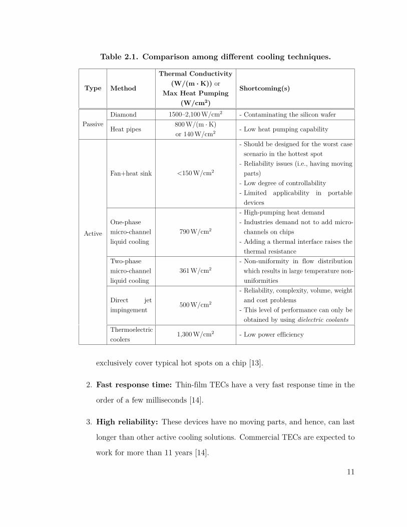
Table 2.1. Comparison among different cooling techniques.
Type Method
Thermal Conductivity(W/(m · K)) or
Max Heat Pumping(W/cm2)
Shortcoming(s)
PassiveDiamond 1500–2,100 W/cm2 - Contaminating the silicon wafer
Heat pipes800 W/(m ·K)or 140 W/cm2 - Low heat pumping capability
Active
Fan+heat sink <150 W/cm2
- Should be designed for the worst casescenario in the hottest spot
- Reliability issues (i.e., having movingparts)
- Low degree of controllability- Limited applicability in portable
devices
One-phasemicro-channelliquid cooling
790 W/cm2
- High-pumping heat demand- Industries demand not to add micro-
channels on chips- Adding a thermal interface raises the
thermal resistanceTwo-phasemicro-channelliquid cooling
361 W/cm2- Non-uniformity in flow distribution
which results in large temperature non-uniformities
Direct jetimpingement
500 W/cm2
- Reliability, complexity, volume, weightand cost problems
- This level of performance can only beobtained by using dielectric coolants
Thermoelectriccoolers
1,300 W/cm2 - Low power efficiency
exclusively cover typical hot spots on a chip [13].
2. Fast response time: Thin-film TECs have a very fast response time in the
order of a few milliseconds [14].
3. High reliability: These devices have no moving parts, and hence, can last
longer than other active cooling solutions. Commercial TECs are expected to
work for more than 11 years [14].
11
4. High controllability: TECs can be controlled at the granularity of fractions
of a degree of Celsius and can cool down a chip below the ambient temperature
[14].
5. Very high heat pumping rate: It has been shown that thin-film TECs
can pump high heat fluxes as large as ∼1,300 W/cm2 [13].
In the next subsection, principles of thermoelectric cooling are explained.* Next,
the assembly of TEC modules inside a microprocessor cooling package is explained.
This assembly is used throughout the first part of the dissertation.
I will show that with careful deployment and control of TECs, good power
efficiencies can be achieved. These techniques along with future advances in TEC
materials pave the way of utilizing TECs as key elements in cooling packages.
2.1.1 Principles of Thermoelectric Cooling
Thermoelectric coolers are compact devices which are made of pairs of N- and
P-type semiconductor pellets. Usually, these pellets are fabricated from properly
doped Bismuth Telluride (Bi2Te3). When current flows through a P-type pellet
(from the positive terminal to the negative terminal), heat flows in the same
direction, i.e., heat is absorbed from the positive side, which is called cold side, and
released to the negative side, which is called hot side. The heat flow direction in an
N-type pellet is the reverse of that in the P-type pellet.
Usually several N-P pairs are connected electrically in series and thermally in
parallel to increase the amount of heat rejection. The reason for serially connecting
TECs is that each TEC pellet can tolerate a very small voltage (around 60 mV),
*Presented equations are well known in the field of thermodynamics. Interested readers mayrefer to reference [21] for detailed discussions.
12
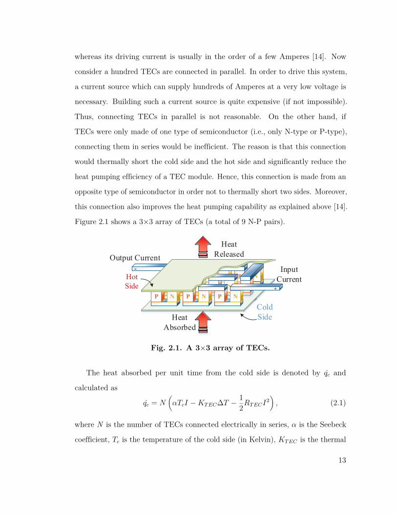
whereas its driving current is usually in the order of a few Amperes [14]. Now
consider a hundred TECs are connected in parallel. In order to drive this system,
a current source which can supply hundreds of Amperes at a very low voltage is
necessary. Building such a current source is quite expensive (if not impossible).
Thus, connecting TECs in parallel is not reasonable. On the other hand, if
TECs were only made of one type of semiconductor (i.e., only N-type or P-type),
connecting them in series would be inefficient. The reason is that this connection
would thermally short the cold side and the hot side and significantly reduce the
heat pumping efficiency of a TEC module. Hence, this connection is made from an
opposite type of semiconductor in order not to thermally short two sides. Moreover,
this connection also improves the heat pumping capability as explained above [14].
Figure 2.1 shows a 3×3 array of TECs (a total of 9 N-P pairs).
NP N P NPNPN
P NP N
PN
P
-
Heat Absorbed
Input Current
Output Current
PN
+
Heat Released
Fig. 2.1. A 3×3 array of TECs.
The heat absorbed per unit time from the cold side is denoted by 𝑞𝑐 and
calculated as
𝑞𝑐 = 𝑁(︂
𝛼𝑇𝑐𝐼 −𝐾𝑇 𝐸𝐶Δ𝑇 − 12𝑅𝑇 𝐸𝐶𝐼2
)︂, (2.1)
where N is the number of TECs connected electrically in series, 𝛼 is the Seebeck
coefficient, 𝑇𝑐 is the temperature of the cold side (in Kelvin), 𝐾𝑇 𝐸𝐶 is the thermal
13
conductance of the TEC, Δ𝑇 is the temperature difference between the hot side
and the cold side (= 𝑇ℎ − 𝑇𝑐), 𝑅𝑇 𝐸𝐶 is the electrical resistance of a single TEC
pellet pair, and 𝐼 is the current which flows through TECs. The first term in this
equation captures the Peltier effect which is the cooling phenomenon, the second
term signifies the heat conductivity of the material from the hot side to the cold
side, and the third term is the Joule heating effect. Note that the second and
the third terms have adverse effects in the cooling applications and hence have a
negative sign. Moreover, the 12 coefficient for the Joule heating is added because it
is approximated that half of the Joule heating is released in the cold side and the
other half is released in the hot side. Also note that the Joule heating quadratically
depends on the current, whereas the Peltier effect linearly depends on it.
Similarly, the heat released per unit time to the hot side is denoted by 𝑞ℎ and
can be written as
𝑞ℎ = 𝑁(︂
𝛼𝑇ℎ𝐼 −𝐾𝑇 𝐸𝐶Δ𝑇 + 12𝑅𝑇 𝐸𝐶𝐼2
)︂, (2.2)
where 𝑇ℎ denotes the temperature of the hot side. In Equations (2.1) and (2.2), the
Thomson effect is not considered due to its negligible effect. Figure 2.2 shows how
the current flows through a TEC N-P pair. The dashed arrow shows the direction
of the current flow.
Power consumption of 𝑁 TECs is the difference between 𝑞ℎ and 𝑞𝑐 and may be
written as follows.
𝑃𝑇 𝐸𝐶,𝑁 = 𝑞ℎ − 𝑞𝑐 = 𝑁(𝑅𝑇 𝐸𝐶𝐼2 + 𝛼Δ𝑇𝐼) (2.3)
The contact resistance between pellets and the metal contact increases the TEC
14
NNPPh
a×b
a×a
ContactResistancesContacts
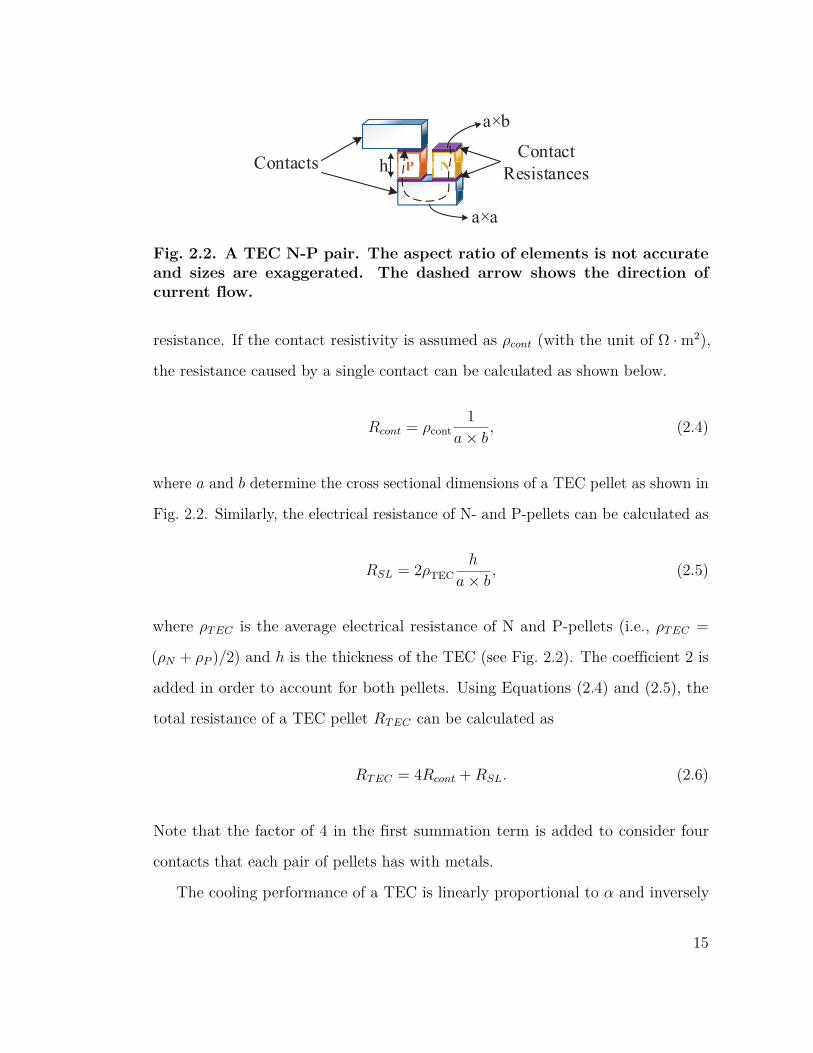
Fig. 2.2. A TEC N-P pair. The aspect ratio of elements is not accurateand sizes are exaggerated. The dashed arrow shows the direction ofcurrent flow.
resistance. If the contact resistivity is assumed as 𝜌𝑐𝑜𝑛𝑡 (with the unit of Ω ·m2),
the resistance caused by a single contact can be calculated as shown below.
𝑅𝑐𝑜𝑛𝑡 = 𝜌cont1
𝑎× 𝑏, (2.4)
where 𝑎 and 𝑏 determine the cross sectional dimensions of a TEC pellet as shown in
Fig. 2.2. Similarly, the electrical resistance of N- and P-pellets can be calculated as
𝑅𝑆𝐿 = 2𝜌TECℎ
𝑎× 𝑏, (2.5)
where 𝜌𝑇 𝐸𝐶 is the average electrical resistance of N and P-pellets (i.e., 𝜌𝑇 𝐸𝐶 =
(𝜌𝑁 + 𝜌𝑃 )/2) and ℎ is the thickness of the TEC (see Fig. 2.2). The coefficient 2 is
added in order to account for both pellets. Using Equations (2.4) and (2.5), the
total resistance of a TEC pellet 𝑅𝑇 𝐸𝐶 can be calculated as
𝑅𝑇 𝐸𝐶 = 4𝑅𝑐𝑜𝑛𝑡 + 𝑅𝑆𝐿. (2.6)
Note that the factor of 4 in the first summation term is added to consider four
contacts that each pair of pellets has with metals.
The cooling performance of a TEC is linearly proportional to 𝛼 and inversely
15
proportional to 𝐾𝑇 𝐸𝐶 and 𝑅𝑇 𝐸𝐶 . Hence a natural way of defining figure of merit
(Z) for a TEC device is
𝑍 = 𝛼2
𝑅𝑇 𝐸𝐶𝐾𝑇 𝐸𝐶
= 𝛼2
𝜌𝑇 𝐸𝐶𝑘𝑇 𝐸𝐶
. (2.7)
The simplification in Eq. (2.7) is done using the relations 𝑅𝑇 𝐸𝐶 = 𝜌𝑇 𝐸𝐶ℎ𝑎𝑏
and
𝐾𝑇 𝐸𝐶 = 𝑘𝑇 𝐸𝐶𝑎𝑏ℎ
. Note that in the second relation, capital 𝐾𝑇 𝐸𝐶 is the thermal
conductance whereas small 𝑘𝑇 𝐸𝐶 is the thermal conductivity. Figure of merit is
defined in such a way to be independent of TEC geometry and its input current.
In order to make this metric a dimensionless quantity, 𝑍𝑇𝑎𝑣𝑔 is usually used. T𝑎𝑣𝑔
is the average temperature between the hot and the cold side temperatures of a
TEC. 𝑍𝑇 𝑎𝑣𝑔 value for the state-of-the-art TECs is as high as 2.1 in 300 K [13].
A common and useful metric is the coefficient of performance which I denote it
as 𝐶𝑂𝑃 𝑏𝑎𝑠𝑖𝑐. This metric is traditionally defined as the ratio of the rejected heat
per unit time (𝑞𝑐) and the input power to 𝑁 TECs:
𝐶𝑂𝑃 𝑏𝑎𝑠𝑖𝑐 = 𝑞𝑐
𝑞ℎ − 𝑞𝑐
= 𝑞𝑐
𝑃𝑇 𝐸𝐶,𝑁
=𝛼𝑇𝑐𝐼 −𝐾𝑇 𝐸𝐶Δ𝑇 − 1
2𝑅𝑇 𝐸𝐶𝐼2
𝛼Δ𝑇𝐼 + 𝑅𝑇 𝐸𝐶𝐼2 (2.8)
2.1.2 TEC Assembly
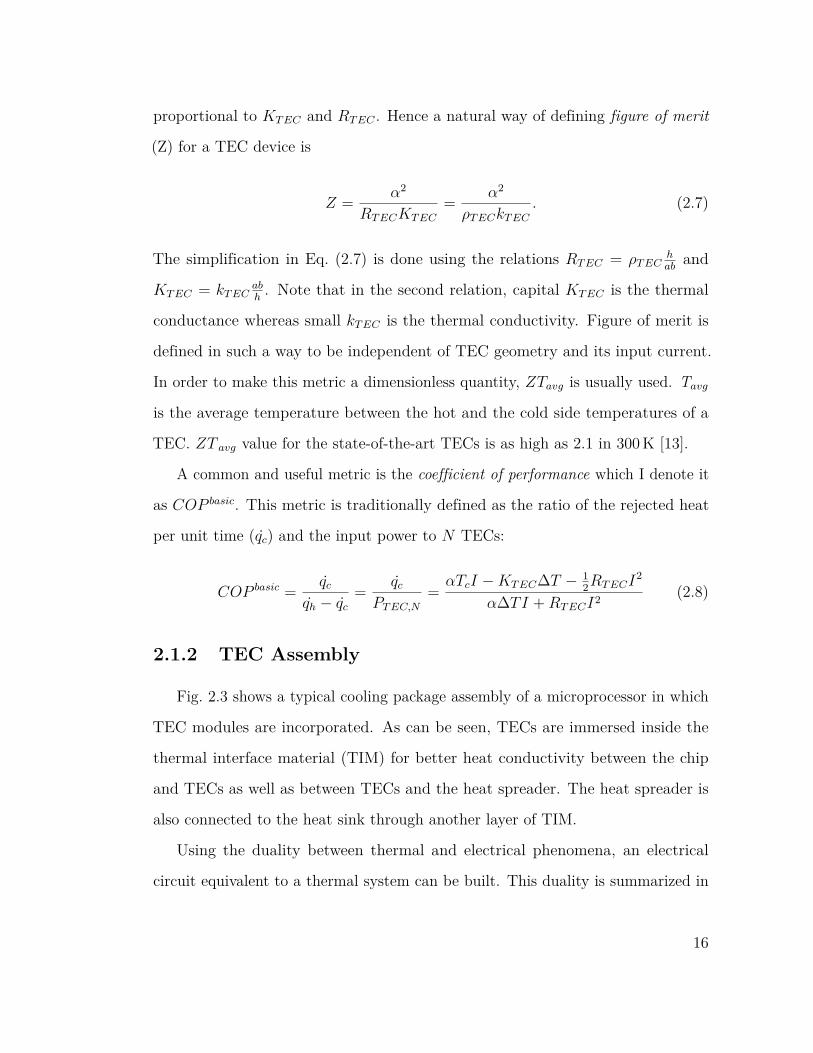
Fig. 2.3 shows a typical cooling package assembly of a microprocessor in which
TEC modules are incorporated. As can be seen, TECs are immersed inside the
thermal interface material (TIM) for better heat conductivity between the chip
and TECs as well as between TECs and the heat spreader. The heat spreader is
also connected to the heat sink through another layer of TIM.
Using the duality between thermal and electrical phenomena, an electrical
circuit equivalent to a thermal system can be built. This duality is summarized in
16
ChipCCChhhiiipCCCCCChhCChhiihhiiippChippPCB
Heat Sink
Fig. 2.3. A chip assembly with its cooling solution
Table 2.2. An electrical system can be easily analyzed using well-known circuit laws
(such as KVL and KCL) and simulated using circuit simulators such as SPICE.
Table 2.2. Thermal quantities and their electrical duals.
Thermal Electrical DualThermal Quantity Unit Quantity UnitTemperature (T) K Voltage (V) VPower (P) W Current (I) AThermal resistance (Rth) K/W Electrical resistance (R) ΩHeat capacity (Cth) J/K Electrical capacitance (C) F
2.1.3 Principles of Thermoelectric Generation
Thermoelectric generators (TEGs) are essentially the same device as thermo-
electric coolers; however, they are working based on the Seebeck effect which is the
dual of the Peltier effect. In other words, when a temperature difference is applied
across TEG pellets, current flows through them. TEGs have unique capabilities,
which have made them a preferable choice compared to conventional energy sources
(such as batteries) and other energy harvesting methods (such as solar cells). TEGs
are:
1. Silent: TEGs have no moving part and are made of semiconductor materials
and hence, generate no noise [22].
17
2. Very durable: TEGs are reported to work for up to 30 years [22], which
makes them ideal for remote or difficult-to-reach locations and the outer
space. For space missions beyond Mars, TEGs are the only means of energy
harvesting, since the sunlight intensity drops significantly [21].
3. Compact and lightweight: Each TEG can be manufactured to be as small
as 0.5𝑚𝑚× 0.5𝑚𝑚× 100𝜇𝑚 [13].
4. Inexpensive: The cost of deploying TEGs compared to large generators or
batteries (considering the replacement cost) is quite low [23].
5. Scalable: TEG modules can be simply connected together to increase the
amount of harvested energy [22].
The direction of generated current in an N-type pellet is opposite of that of
a P-type pellet. Hence, to improve the amount of harvested energy and increase
the overall generated voltage, these pellets are connected in a zig-zag manner (see
Fig. 2.4), i.e., they are connected electrically in series and thermally in parallel
(similar to that of TECs).
Fig. 2.4 depicts a 3× 3 array of TEG pellet pairs (a total of 9 pairs) connected
to a load, which is usually a converter circuitry to interface between TEGs and the
energy storage element. When a temperature gradient is applied to this module
such that the bottom side (hot side) becomes hotter than the top side (cold side),
current flows through the load in the counterclockwise direction.
The total electrical resistance of a TEG pellet can be calculated similar to that
of a TEC pellet (see Eq. (2.6)). The generated voltage by 𝑁 TEGs is called Seebeck
voltage and can be formulated as
𝛼𝑁Δ𝑇, (2.9)
18
Hot Side
Load
NP N P NPNPN
P NP N
PN
P
+
Heat flow (in)
PN
-
Heat flow (out)
Generated Current
Fig. 2.4. A 3× 3 TEG module connected to a load.
where 𝛼𝑁 is the Seebeck coefficient of 𝑁 pellet pairs and Δ𝑇 is the temperature
difference across them. The heat flow rate through the hot side of a TEG module
(𝑞ℎ) and its cold side (𝑞𝑐) which result in the generation of current 𝐼 may be
formulated as
𝑞ℎ = Δ𝑇
Θ𝑇 𝐸𝐺,𝑁
− 𝛼𝑁𝐼𝑇ℎ −12𝑅𝑇 𝐸𝐺,𝑁𝐼2 and (2.10)
𝑞𝑐 = Δ𝑇
Θ𝑇 𝐸𝐺,𝑁
− 𝛼𝑁𝐼𝑇𝑐 + 12𝑅𝑇 𝐸𝐺,𝑁𝐼2. (2.11)
In these equations, 𝑅𝑇 𝐸𝐺,𝑁 and Θ𝑇 𝐸𝐺,𝑁 are the electrical and thermal resistances
of 𝑁 pairs of TE pellets. Note that Θ𝑇 𝐸𝐺,𝑁 = 1𝐾𝑇 𝐸𝐺,𝑁
, where 𝐾𝑇 𝐸𝐺,𝑁 is the thermal
conductance of 𝑁 pairs of TE pellets. In this dissertation, the subscript 𝑁 is used
to denote a parameter describing 𝑁 TE pairs, whereas parameters without it are
related to only one pair. Accordingly, the following relations hold:
𝛼𝑁 = 𝑁 × 𝛼, (2.12)
𝑅𝑇 𝐸𝐺,𝑁 = 𝑁 ×𝑅𝑇 𝐸𝐺, and (2.13)
19
Θ𝑇 𝐸𝐺,𝑁 = Θ𝑇 𝐸𝐺
𝑁. (2.14)
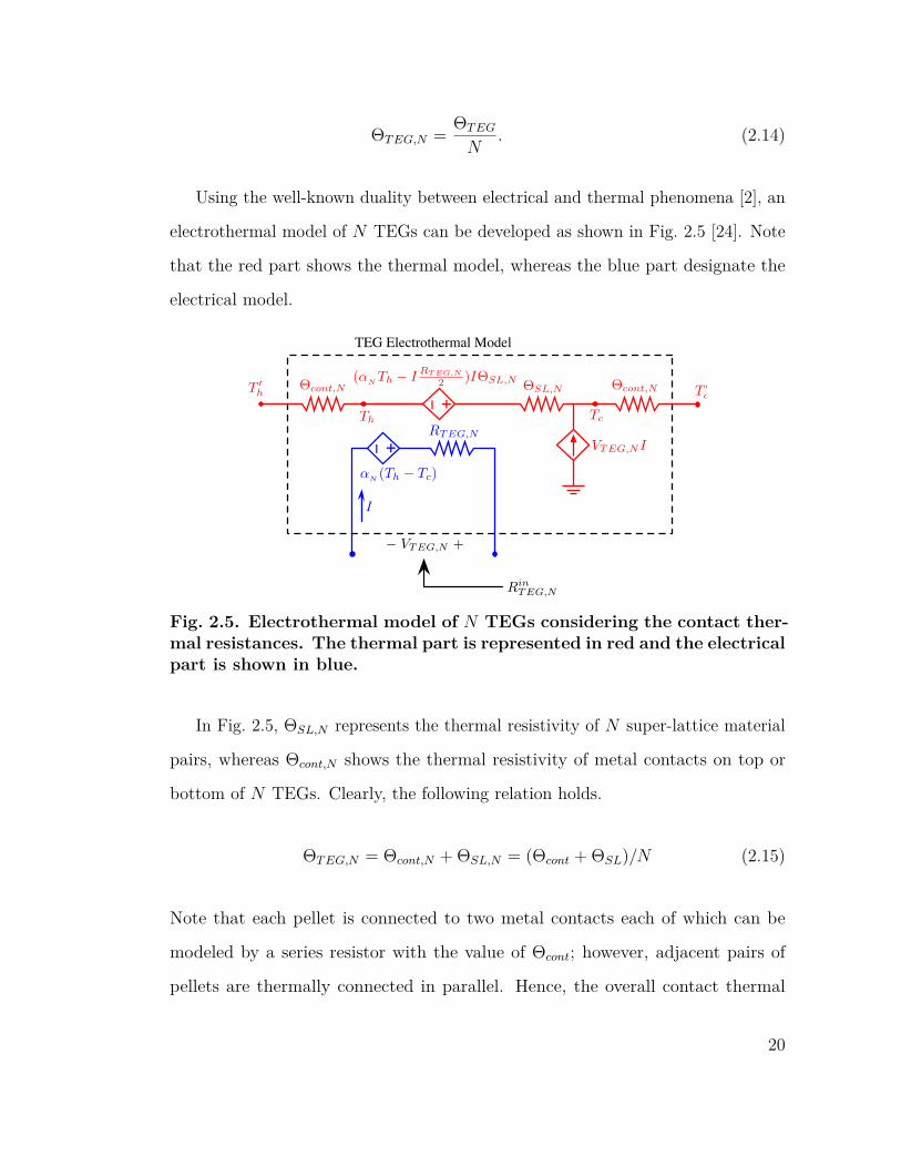
Using the well-known duality between electrical and thermal phenomena [2], an
electrothermal model of 𝑁 TEGs can be developed as shown in Fig. 2.5 [24]. Note
that the red part shows the thermal model, whereas the blue part designate the
electrical model.
VTEG,NI
(↵N
Th � IRT EG,N
2 )I⇥SL,N
RTEG,N
↵N
(Th � Tc)
Th Tc
⇥SL,N ⇥cont,N⇥cont,NT 0h T 0
c
TEG Electrothermal Model
RinTEG,N
I
� VTEG,N +
= +
= +
Fig. 2.5. Electrothermal model of 𝑁 TEGs considering the contact ther-mal resistances. The thermal part is represented in red and the electricalpart is shown in blue.
In Fig. 2.5, Θ𝑆𝐿,𝑁 represents the thermal resistivity of 𝑁 super-lattice material
pairs, whereas Θ𝑐𝑜𝑛𝑡,𝑁 shows the thermal resistivity of metal contacts on top or
bottom of 𝑁 TEGs. Clearly, the following relation holds.
Θ𝑇 𝐸𝐺,𝑁 = Θ𝑐𝑜𝑛𝑡,𝑁 + Θ𝑆𝐿,𝑁 = (Θ𝑐𝑜𝑛𝑡 + Θ𝑆𝐿)/𝑁 (2.15)
Note that each pellet is connected to two metal contacts each of which can be
modeled by a series resistor with the value of Θ𝑐𝑜𝑛𝑡; however, adjacent pairs of
pellets are thermally connected in parallel. Hence, the overall contact thermal
20
resistance for each adjacent pair of pellets is equal to Θ𝑐𝑜𝑛𝑡 (i.e., there are two
parallel resistances with the value of 2Θ𝑐𝑜𝑛𝑡).
2.2 Prior Work
2.2.1 Thermoelectric Coolers
Many studies have been conducted in the area of thermal management of VLSI
dies using TECs. These studies mainly have focused on two issues. First, improving
the manufacturing process of a TEC in order to increase the figure of merit (𝑍).
For instance, Bar-Cohen and Wang [12] present a comprehensive survey on TEC
principles and the manufacturing advances in recent years. Besides, Hou et al. [25]
try to improve the performance of TECs by optimizing the dimensions of N- and
P-pellets. Second, adopting TECs in a cooling system to improve the cooling
efficiency. My work focuses on the second subject and hence, the relevant literature
is reviewed next.
Biswas et al. [26] use TECs in order to cool down microprocessors in a data
center and reduce the total cooling cost while maintaining high reliability. They
mainly focus on the steady-state analysis of TECs and uses a constant coefficient
of performance (𝐶𝑂𝑃 𝑏𝑎𝑠𝑖𝑐) for modeling TECs. This method is inaccurate and too
coarse grain. Moreover, the fan speed and its power consumption are assumed to
be constant.
Bierschenk amd Johnson [27] try to increase 𝐶𝑂𝑃 𝑏𝑎𝑠𝑖𝑐 by restricting the Δ𝑇
to smaller values. However, this is not a practical solution in the microprocessor
cooling application, because TECs are sandwiched between the heat spreader and
the TIM and as a result 𝑇ℎ cannot be directly controlled. One can still use a better
heat sink and fan assembly in order to insure that 𝑇ℎ does not go beyond a certain
21
value. This solution is not cost efficient and sometimes due to the system form
factor, it is not possible to install a larger heat sink or a fan.
Alexandrov et al. [28] show the significance of the transient behavior of TECs in
VLSI die cooling. They present two simple controllers: A threshold based controller,
which turns on or off TECs when the temperature goes above or below a certain
temperature, and a maximum cooling based controller, which uses the hysteresis
effect to decrease the number of on/off transitions of TECs. In both controllers,
TECs are supplied with a constant current to effect a state change.
Long et al. [29] formulates the selective deployment of TECs on top of a chip in
order to achieve the maximum cooling (i.e., the lowest temperature). The motivation
is that excessive deployment of TECs adversely affects the temperature of the
device because of lateral heating among TECs. Moreover, deploying unnecessary
TECs increases the power consumption of the cooling solution. This work considers
only the spatial distribution of TECs.
In another work, Long et al. [30] suggest independent control of TECs by
multiple current sources. Adding several current sources leads to the addition of
input pins to the chip which is costly. Consequently, authors show that with only
three or four independent current sources, the temperature of the hottest spot
on average is no higher than the case where infinite number of current sources
are available (i.e., each TEC can be controlled independently) by 0.6 ∘C or 0.3 ∘C,
respectively. Similar to their prior work [29], [30] does not consider the temporal
distribution of hot spots. Moreover, the target processor in these two articles is a
single-core processor, which does not exhibit significant non-uniformity in temporal
and spatial distributions of hot spots compared to a multi-core processor. The focus
of these two papers (i.e., [29] and [30]) is on the steady-state analysis of TECs.
Murali et al. [5, 6] formulate the dynamic thermal management problem as a
22
convex optimization in which the objective function is the total throughput of
the system (which has to be maximized). The chip power consumption and die
temperature are constraints of the problem formulation. Optimization variables
are frequencies of CPU cores. Note that no active cooling technology is considered
in these two papers.
Shin et al. [31] consider the fan speed, CPU frequency, and supply voltage as
optimization variables in order to minimize the total energy consumption of the
system. However, the thermoelectric cooling technique is not considered. Moreover,
a lumped thermal model for a processor is adopted which sacrifices the accuracy
of the model at the cost of a simplified model. Furthermore, this simplification
may leave hot spots on the chip since the lumped model considers the average
temperature for the entire processor die.
Paterna and Reda [32] identify high-spatial power densities as one of the key
problems that leads to the dark silicon issue in multi-core processors. They propose
a non-linear program which leverages TECs along with dynamic voltage and
frequency (DVFS) and the number of active threads in order to maximize the
performance of a multi-core processor under the power and thermal constraints.
The performance is defined as the summation of the instruction-per-cycle (IPC)
times the frequency of each core.
Rho et al. [33] adopt TECs along with DVFS for cooling 3D ICs. With their
setup, they reduce the total energy consumption of the processor and TECs
compared to a processor without TECs by 20%. This reduction is achieved due to
the saving of leakage power.
23
2.2.2 Thermoelectric Generators
Research on thermoelectric generators is mainly divided into two parts. First,
the manufacturing and assembly techniques in order to maximize TEG’s figure
of merit. Second, designing the interface circuitry for maximally transferring the
generated power to the load. The focus of this dissertation is on the latter part.
Much work has been conducted on designing interface circuitries. Even though
the electrothermal model of TEGs are constructed (e.g., [24]), the internal resistance
of 𝑁 TEGs (𝑅𝑖𝑛𝑇 𝐸𝐺,𝑁) is claimed to be equal to the electrical resistance of the
thermoelectric material plus its associated contacts (𝑅𝑇 𝐸𝐺,𝑁). This modeling
neglects the thermal resistance of TEG contacts and its effect on 𝑅𝑖𝑛𝑇 𝐸𝐺,𝑁 . Here, I
enumerate a few examples that consider 𝑅𝑖𝑛𝑇 𝐸𝐺,𝑁 to be equal to 𝑅𝑖𝑛
𝑇 𝐸𝐺,𝑁 .
The basic equations for the amount of power that can be extracted from TEGs
are explained in books [21] and [34]. In order to maximize the extracted power, it
is claimed that the load should be matched with the electrical resistivity of a TEG
module.
Solbrekken et al. [35] present a system design which utilizes TEGs in order to
harvest the heat produced by a laptop CPU. With careful thermal isolation for
maximizing the temperature difference across TEG sides, they manage to use this
energy to drive a fan in order to cool down the CPU. This paper also uses the
electrical resistance of TEGs and adopts it to determine the internal resistance of
TEGs.
Lu et al. [36] present a design framework for charge pump converters connected
to TEGs. Different sources of power loss are characterized and considered in the
design. This paper also uses the electrical resistivity of TEGs to make their Thévenin
equivalent circuit. As I will explain in Chapter 6, since TEGs are non-linear circuits,
the Thévenin theorem does not apply to them.
24
Accurate internal resistance modeling of TEGs allow me to devise a maximum
power point tracking (MPPT) technique. There are many MPPT techniques
developed mostly for photovoltaics, such as current sweep, fractional 𝑉𝑂𝐶† and
𝐼𝑆𝐶‡, array reconfiguration, and so on. Esram et al. [37] provide an excellent survey
of these methods. Some of these techniques are general and can be used for TEGs
as well. However, most of the techniques require sensing of open circuit voltage
(𝑉 𝑜𝑐𝑇 𝐸𝐺,𝑁), current (𝐼), or both. On the other hand, the MPPT algorithm proposed
in Chapter 6 only requires temperature sensors. Consequently, this algorithm does
not require to periodically disrupt and disconnect the power harvesting module in
order to sense the open circuit voltage.
†𝑉𝑂𝐶 : Open circuit voltage‡𝐼𝑆𝐶 : Short circuit current
25
3Thermoelectric Cooler-Based Systems Analysis
3.1 Overview
A major drawback of TECs is their rather poor coefficient of performance
(COP), which is defined as the ratio of heat removed in a unit of time to the total
power used to drive TECs. Many studies have been focused on adapting TECs for
microprocessor cooling. Sharp et al. [38] suggest to counter the low-COP problem
of TECs by limiting their use to chip hot spots. Accordingly, very few TECs are
selectively deployed on the chip surface. Although this recommendation has been
widely accepted, it has two shortcomings:
1. It limits the usage of TECs to high-performance applications since low-power
applications remain sensitive to low COP values of even a small number of
deployed TECs.
2. Recent state-of-the-art multi-core chips have dozens of hot spots, which
demand aggressive deployment of TECs. Again the low COP value of TECs
poses a serious problem.
In this chapter, I take on the challenge of improving the COP of TECs incorpo-
rated in a processor package. In particular, first I redefine the COP in order to
26
capture the effect of chip leakage power, which is exponentially dependent on the
die temperature. Using this new definition, I show that the COP of a cooling system
(comprised of the chip, TEC elements, and a heat sink) versus the TEC driving
current changes so as to exhibit a peak value for a driving current level based on the
thermal chip condition. This is in clear contrast to the traditional COP vs. current
curve (i.e., when excluding the leakage power consumption from consideration),
which shows a constant peak value irrespective of chip condition. In particular, I
show that TECs can increase the COP of a cooling system by 7% while decreasing
the temperature by 6 ∘C. Using these observations, I present a platform-dependent,
leakage-aware policy to apply an appropriate current level to TECs based on the
target platform/application (i.e., high-performance vs. low-power) and the actual
condition of the chip (i.e., emergency vs. preventive thermal management).
The rest of this chapter is organized as follows. Section 3.2 introduces a new
formulation for COP to account for the leakage power dissipation. Next, Section 3.3
presents the platform-dependent, leakage-aware policy for setting the current of
TECs. After that, Section 3.4 presents the experimental results performed by a
TEC simulator (called Teculator) which is developed based on the suggested new
COP formulation. Finally, Section 3.5 summarizes the chapter.
3.2 Redefining the COP
The major drawback of TECs is their low 𝐶𝑂𝑃 𝑏𝑎𝑠𝑖𝑐. Any value lower than one
means the device adds more heat to the system than the cooling it provides. Even
𝐶𝑂𝑃 𝑏𝑎𝑠𝑖𝑐 values slightly higher than one are problematic since the system would
require a larger heat sink and/or a stronger fan to dissipate the excessive heat
that is generated by TECs. Differentiating the 𝐶𝑂𝑃 𝑏𝑎𝑠𝑖𝑐 defined in Eq. (2.8) with
27
respect to I gives the current value that maximizes the 𝐶𝑂𝑃 𝑏𝑎𝑠𝑖𝑐 [12, 38]. This
current is called 𝐼𝐶𝑂𝑃 (𝑏𝑎𝑠𝑖𝑐),𝑜𝑝𝑡 and is equal to
𝐼𝐶𝑂𝑃 (𝑏𝑎𝑠𝑖𝑐),𝑜𝑝𝑡 = 𝛼Δ𝑇
𝑅𝑇 𝐸𝐶,𝑁
√︁𝑍𝑇𝑎𝑣𝑔 + 1− 1
, (3.1)
where 𝑇𝑎𝑣𝑔 is defined as the average of 𝑇ℎ and 𝑇𝑐. Plugging 𝐼𝐶𝑂𝑃 (𝑏𝑎𝑠𝑖𝑐),𝑜𝑝𝑡 into
Eq. (2.8) gives the maximum value of 𝐶𝑂𝑃 𝑏𝑎𝑠𝑖𝑐, which may be written as
𝐶𝑂𝑃 𝑏𝑎𝑠𝑖𝑐𝑚𝑎𝑥 =
𝑇𝑐
⎛⎜⎜⎝√︁1 + 𝑍𝑇𝑎𝑣𝑔 −𝑇ℎ
𝑇𝑐
⎞⎟⎟⎠Δ𝑇
(︁1 +
√︁1 + 𝑍𝑇𝑎𝑣𝑔
)︁ . (3.2)
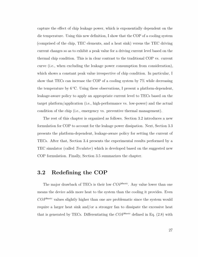
As can be seen, 𝐶𝑂𝑃 𝑏𝑎𝑠𝑖𝑐𝑚𝑎𝑥 is proportional to 𝑇𝑐 and 𝑍𝑇𝑎𝑣𝑔. Moreover, it is
inversely proportional to Δ𝑇 . These relations suggest three ways for increasing
𝐶𝑂𝑃 𝑏𝑎𝑠𝑖𝑐𝑚𝑎𝑥 :
1. Using materials with high figure of merit: This can be done by selecting
better materials and improving fabrication techniques. These methods are
outside the scope of this dissertation.
2. Limiting Δ𝑇 to low values: As it has been discussed previously, this
solution is not possible in many applications/platforms.
3. Increasing 𝑇𝑐: An important observation is that TECs perform efficiently
when 𝑇𝑐 reaches its maximum physically tolerable value.
Fig. 3.1 shows the dependency of 𝐶𝑂𝑃 𝑏𝑎𝑠𝑖𝑐𝑚𝑎𝑥 on the aforementioned parameters.
As can be seen, in order to achieve 𝐶𝑂𝑃 𝑏𝑎𝑠𝑖𝑐𝑚𝑎𝑥 values higher than 4, Δ𝑇 should be
limited to ∼15–25 ∘C.
28
∆T (K)
0 10 20 30 40 50
CO
Pb
asic
ma
x
0
2
4
6
8
10
ZTavg
=1, Tc=300 K
ZTavg
=1, Tc=400 K
ZTavg
=2, Tc=300 K
ZTavg
=2, Tc=400 K
Fig. 3.1. Dependency of 𝐶𝑂𝑃 𝑏𝑎𝑠𝑖𝑐𝑚𝑎𝑥 on Δ𝑇 , 𝑍𝑇𝑎𝑣𝑔, and 𝑇𝑐.
Increasing 𝑇𝑐 is a possible solution for some applications (other than processor
cooling). However, for cooling electronic circuits, it comes at the cost of increasing
the leakage power, which is exponentially dependent on the die temperature [1].
Unfortunately, the 𝐶𝑂𝑃 𝑏𝑎𝑠𝑖𝑐 does not capture the effect of the leakage power.
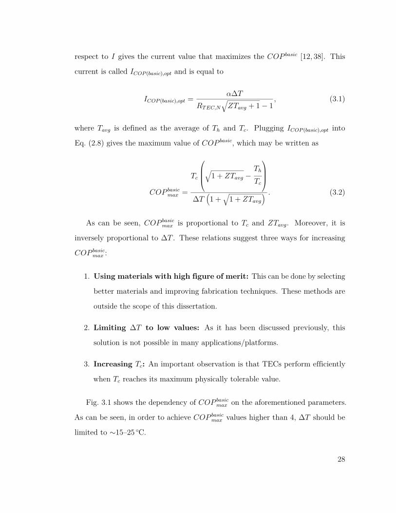
Based on the thermal/electrical duality explained in Chapter 2, a TEC inside a
processor package can be modeled using an electrical circuit. This model is shown
in Fig. 3.2. The Peltier effect is modeled by two current sources: one is at the
bottom which has a negative value, and hence, absorbs heat and one is at the
top which has a positive value and releases heat. The Joule heating effect is also
modeled as a current source which charges a capacitor. This capacitor signifies the
specific heat of the TEC material. When a TEC is turned on (or its driving current
is changed), the Peltier effect appears quickly but the Joule heating effect appears
gradually. The reason is that the Joule heating needs to overcome the specific heat
of the TEC material (i.e., charges the capacitor), whereas the Peltier effect only
pumps heat from one side to the other side [28,39]. The two RC networks model
the rest of thermal package at the top and bottom of the TEC. The novelty in this
29
model is the addition of 𝑃𝑙𝑒𝑎𝑘𝑎𝑔𝑒 as a function of 𝑇𝑑𝑖𝑒. Note that the temperature
which affects the leakage power (𝑇𝑑𝑖𝑒) is not equal to 𝑇𝑐 but it is a function of it.
K/2
K/2RTECI2 CTEC
-αITc
αITh
Tc
Th
TEC
Pleakage(Tdie)
RC Network
Pdynamic
RC Network Tambient
Fig. 3.2. An electrical model for a TEC embedded inside a processorpackage.
Using the model given above, the system COP or 𝐶𝑂𝑃 𝑠𝑦𝑠, which captures the
die temperature-dependent leakage power of the system, is written as
𝐶𝑂𝑃 𝑠𝑦𝑠 =𝑁(︁𝛼𝑇𝑐𝐼 −𝐾𝑇 𝐸𝐶Δ𝑇 − 1
2𝑅𝑇 𝐸𝐶𝐼2)︁− 𝑃𝑙𝑒𝑎𝑘𝑎𝑔𝑒(𝑇𝑑𝑖𝑒)
𝑁 (𝛼Δ𝑇𝐼 + 𝐼2𝑅𝑇 𝐸𝐶) + 𝑃𝑙𝑒𝑎𝑘𝑎𝑔𝑒(𝑇𝑑𝑖𝑒). (3.3)
The leakage power decreases the amount of cooling (nominator) and increases
the power consumption of the TEC (denominator). The 𝐶𝑂𝑃 𝑠𝑦𝑠 is equal to zero
when the cooling and heating amounts are identical. Note that in this formulation,
𝑃𝑑𝑦𝑛𝑎𝑚𝑖𝑐 is not considered for the system as its value is not controlled by the
TEC (neither directly by the TEC current nor indirectly by the temperature).
Maximizing the 𝐶𝑂𝑃 𝑠𝑦𝑠 is equivalent to achieving the maximum cooling while
30
expending the least amount of power; this is called the maximum COP cooling
(MCPC) strategy. Defining the 𝐶𝑂𝑃 𝑠𝑦𝑠 helps find the MCPC current for driving
TECs. This current is a function of the leakage power and it changes based on
the chip condition, whereas the 𝐶𝑂𝑃 𝑏𝑎𝑠𝑖𝑐 is independent of the chip condition.
Differentiating Eq. (3.3) with respect to 𝐼 does not give a closed-form expression
for 𝐼𝐶𝑂𝑃 (𝑠𝑦𝑠),𝑜𝑝𝑡 like the one presented in Eq. (3.1). As a result, I perform different
experiments with several current values to find the one that maximizes the 𝐶𝑂𝑃 𝑠𝑦𝑠.
Although this method seems to be time consuming, in fact it is not an expensive
proposition, because this is done offline during the design phase.
3.3 Platform-Dependent, Leakage-Aware Cool-
ing Policy for TECs
As it will be demonstrated in the next section, the driving current of TECs for the
MCPC strategy is quite different from that of the maximum temperature reduction
(MTR) strategy. Based on this observation, one can establish a platform-dependent,
leakage-aware cooling policy according to the target platform/application (i.e.,
high-performance vs. low-power). The first target platform (i.e., high-performance)
employs the MTR policy, whereas the second one (i.e., low-power) adopts the
MCPC strategy. The optimum current which is suitable for the MTR case is called
𝐼𝑀𝑇 𝑅 and the optimum current for the MCPC case is called 𝐼𝑀𝐶𝑃 𝐶 . As explained
previously, the Peltier effect appears before the Joule heating. This behavior is
usually used for transient cooling. Hence, for each platform type, a set of currents
should be found; one that works best in the steady-state and another one which is
suitable for the transient cooling.
31
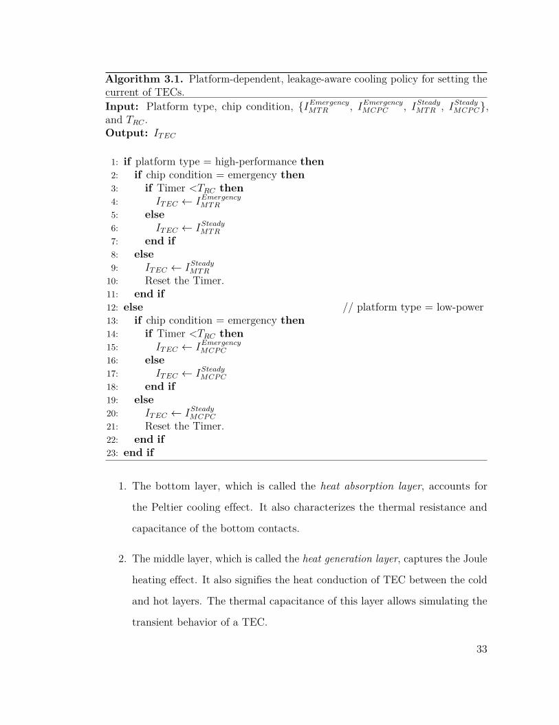
Based on the aforementioned explanations, Algorithm 3.1 describes a platform-
dependent, leakage-aware cooling algorithm, which determines the TEC driving
current for both steady-state and transient regimes of operation. In this algorithm,
platform type is set based on requirements of the target hardware or application;
chip condition refers to the current die temperature, which can be read from
temperature sensors deployed on the chip surface. The set of TEC currents for
different conditions and the thermal network time constant (𝑇𝑅𝐶) are determined
based on a thorough analysis of the TEC thermal behavior. Note that one can
extend this algorithm to provide an (online) adaptive cooling policy, which uses
a peak COP tracking method (via a look-up table or an online optimizer) in
order to set the driving current of TECs at a finer time granularity based on
dynamically-updated die temperatures.
Transient cooling is superior only for the duration of 𝑇𝑅𝐶 , hence, a timer is set
up in order to stop using transient current if the emergency condition lasts more
than 𝑇𝑅𝐶 . Without this timer, if the emergency situation takes longer than 𝑇𝑅𝐶 ,
the Joule heating effect will dominate the Peltier effect and the policy will not
perform well.
3.4 Experiments and Discussion
3.4.1 Simulation Setup
To evaluate the new definition of COP and find the optimum TEC current
values for the proposed cooling algorithm, I developed a tool called Teculator (i.e.,
a TEC Simulator) to simulate the behavior of TECs and evaluate their effect
in a processor package assembly. This tool is implemented as an extension to
HotSpot 5 [40]. Each TEC is modeled in three layers:
32
Algorithm 3.1. Platform-dependent, leakage-aware cooling policy for setting thecurrent of TECs.Input: Platform type, chip condition, {𝐼𝐸𝑚𝑒𝑟𝑔𝑒𝑛𝑐𝑦
𝑀𝑇 𝑅 , 𝐼𝐸𝑚𝑒𝑟𝑔𝑒𝑛𝑐𝑦𝑀𝐶𝑃 𝐶 , 𝐼𝑆𝑡𝑒𝑎𝑑𝑦
𝑀𝑇 𝑅 , 𝐼𝑆𝑡𝑒𝑎𝑑𝑦𝑀𝐶𝑃 𝐶},
and 𝑇𝑅𝐶 .Output: 𝐼𝑇 𝐸𝐶
1: if platform type = high-performance then2: if chip condition = emergency then3: if Timer <𝑇𝑅𝐶 then4: 𝐼𝑇 𝐸𝐶 ← 𝐼𝐸𝑚𝑒𝑟𝑔𝑒𝑛𝑐𝑦
𝑀𝑇 𝑅
5: else6: 𝐼𝑇 𝐸𝐶 ← 𝐼𝑆𝑡𝑒𝑎𝑑𝑦
𝑀𝑇 𝑅
7: end if8: else9: 𝐼𝑇 𝐸𝐶 ← 𝐼𝑆𝑡𝑒𝑎𝑑𝑦
𝑀𝑇 𝑅
10: Reset the Timer.11: end if12: else // platform type = low-power13: if chip condition = emergency then14: if Timer <𝑇𝑅𝐶 then15: 𝐼𝑇 𝐸𝐶 ← 𝐼𝐸𝑚𝑒𝑟𝑔𝑒𝑛𝑐𝑦
𝑀𝐶𝑃 𝐶
16: else17: 𝐼𝑇 𝐸𝐶 ← 𝐼𝑆𝑡𝑒𝑎𝑑𝑦
𝑀𝐶𝑃 𝐶
18: end if19: else20: 𝐼𝑇 𝐸𝐶 ← 𝐼𝑆𝑡𝑒𝑎𝑑𝑦
𝑀𝐶𝑃 𝐶
21: Reset the Timer.22: end if23: end if
1. The bottom layer, which is called the heat absorption layer, accounts for
the Peltier cooling effect. It also characterizes the thermal resistance and
capacitance of the bottom contacts.
2. The middle layer, which is called the heat generation layer, captures the Joule
heating effect. It also signifies the heat conduction of TEC between the cold
and hot layers. The thermal capacitance of this layer allows simulating the
transient behavior of a TEC.
33
3. The top layer, which is called the heat rejection layer, models the heat
rejection. Similar to the cold layer, it accounts for the thermal resistance and
capacitance of the top contacts.
TEC parameters are mostly taken from [13]. Missing parameters are taken
from other references that use a similar experimental setup. Table 3.1 lists all TEC
parameters used in simulations. The only missing information for calculating 𝑅𝑇 𝐸𝐶
is the area of N and P-pellets. Using the 92% packing factor (which is reported
in [41]), it can be estimated that 46% of the total area of a TEC is occupied by a
P-pellet and another 46% is occupied by an N-pellet. Based on this ‘assumption’
and Eq. (2.6), 𝑅𝑇 𝐸𝐶 is estimated as 4.98× 10⁻³ Ω.
The processor package assembly used for simulations has a similar configuration
to Fig. 2.3 except the fact that it does not have a fan. Table 3.2 shows dimensions,
thermal resistivity, and specific heat of each layer (except the TEC layer, which
was discussed earlier). The surface of the chip is tiled with 16×16 TECs (a total of
256 TECs). All of these TECs are connected serially and driven by the exact same
current value.
Table 3.1. TEC parameters used in the simulations.
Parameter ValueSeebeck coefficient (𝛼) 3.01× 10⁻⁴ V/KTEC electrical resistivity (𝜌) 1.08× 10⁻⁵ Ω ·m2
TEC thermal conductivity (k) 1.2 W/(m ·K)TEC specific heat capacity (C) [39] 1.20× 10⁶ J/(m3 ·K)TEC dimension [13] [42] 0.5 mm × 0.5 mm × 8 µmTEC contact dimension (each side) 0.5 mm × 0.5 mm × 46 µmTEC-metal contact thermal resistivity 8× 10⁻⁶ m2 ·K/WTEC-metal contact electrical resistivity 10× 10−10 Ω ·m2
McPat [43] is used in order to estimate 𝑃𝑙𝑒𝑎𝑘𝑎𝑔𝑒(𝑇𝑑𝑖𝑒). A Xeon processor (whose
model comes with the tool) is simulated using the 32 nm CMOS process technology.
34
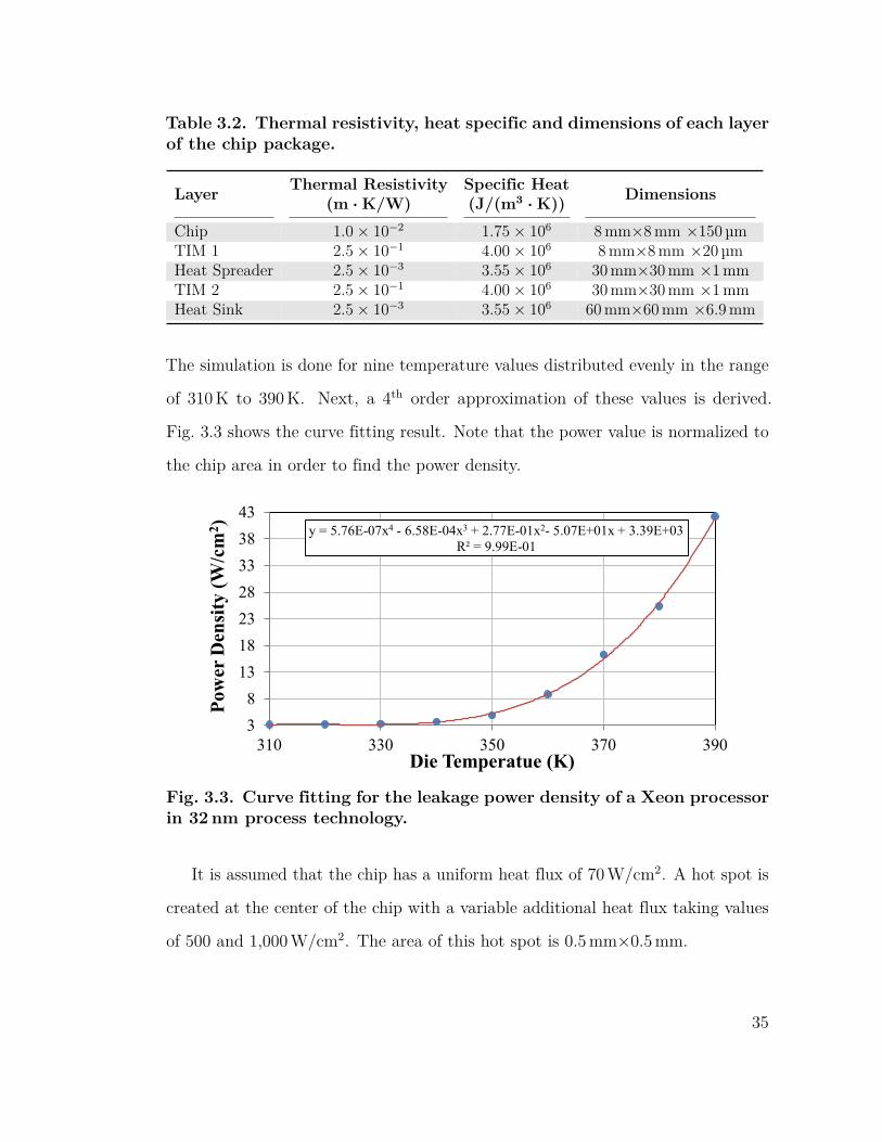
Table 3.2. Thermal resistivity, heat specific and dimensions of each layerof the chip package.
Layer Thermal Resistivity(m · K/W)
Specific Heat(J/(m3 · K)) Dimensions
Chip 1.0× 10⁻² 1.75× 10⁶ 8 mm×8 mm ×150 µmTIM 1 2.5× 10⁻¹ 4.00× 10⁶ 8 mm×8 mm ×20 µmHeat Spreader 2.5× 10⁻³ 3.55× 10⁶ 30 mm×30 mm ×1 mmTIM 2 2.5× 10⁻¹ 4.00× 10⁶ 30 mm×30 mm ×1 mmHeat Sink 2.5× 10⁻³ 3.55× 10⁶ 60 mm×60 mm ×6.9 mm
The simulation is done for nine temperature values distributed evenly in the range
of 310 K to 390 K. Next, a 4th order approximation of these values is derived.
Fig. 3.3 shows the curve fitting result. Note that the power value is normalized to
the chip area in order to find the power density.
y = 5.76E-07x4 - 6.58E-04x3 + 2.77E-01x2- 5.07E+01x + 3.39E+03R² = 9.99E-01
38
13182328333843
310 330 350 370 390
Pow
er D
ensi
ty (W
/cm
2 )
Die Temperatue (K)
Fig. 3.3. Curve fitting for the leakage power density of a Xeon processorin 32 nm process technology.
It is assumed that the chip has a uniform heat flux of 70 W/cm2. A hot spot is
created at the center of the chip with a variable additional heat flux taking values
of 500 and 1,000 W/cm2. The area of this hot spot is 0.5 mm×0.5 mm.
35
3.4.2 Simulation Results
Fig. 3.4(a–d) show the result of several steady-state experiments with different
TEC current values ranging from 0 A to 11 A. For every current value, two local
heat fluxes (hot spots), i.e., 500 and 1,000 W/cm2, are considered. Fig. 3.4(a)
shows the temperature of hot spot. It can be seen that for both heat flux values,
𝐼𝑇 𝐸𝐶=5 A gives the maximum temperature decrease compared to the 𝐼𝑇 𝐸𝐶=0 A
case. This decrease is equal to 14.7 ∘C and 14.2 ∘C for the high and low heat flux
cases, respectively. An interesting point is that the amount of temperature drop
for the high heat flux case is somewhat larger than that of the low heat flux case.
This confirms the claim that TECs work better in higher temperatures. As a result
of this experiment, 𝐼𝑆𝑡𝑒𝑎𝑑𝑦𝑀𝑇 𝑅 is set to 5 A.
Fig. 3.4(b) shows the 𝐶𝑂𝑃 𝑠𝑦𝑠 for different current values. It can be seen that
𝐼𝑇 𝐸𝐶=1 A maximizes the 𝐶𝑂𝑃 𝑠𝑦𝑠 for both heat fluxes. This experiment reveals
four important points:
1. The current value that maximizes the 𝐶𝑂𝑃 𝑠𝑦𝑠 is not equal to the current
that maximizes the temperature decrease. This emphasizes the distinction
between two different objectives, i.e., MTR and MCPC.
2. It is interesting that the 𝐶𝑂𝑃 𝑠𝑦𝑠 has a value higher than unity when 𝐼𝑇 𝐸𝐶=0 A,
i.e., the TECs eventually cools the chip even when they are off. This is due to
the high heat conductivity of TECs. In other words, considering Eq. (3.3), Δ𝑇
takes a negative value, which leads to a large positive value for the 𝐶𝑂𝑃 𝑠𝑦𝑠.
Note that the 𝐶𝑂𝑃 𝑏𝑎𝑠𝑖𝑐 (which is not shown in the figure) does not behave
in the same way as the 𝐶𝑂𝑃 𝑠𝑦𝑠. Indeed, the 𝐶𝑂𝑃 𝑏𝑎𝑠𝑖𝑐 is undefined when
the current is equal to zero since the denominator is equal to zero. Hence,
this second point could not be stated if the 𝐶𝑂𝑃 𝑏𝑎𝑠𝑖𝑐 were used instead of
36
the 𝐶𝑂𝑃 𝑠𝑦𝑠. Moreover, note that the 𝐶𝑂𝑃 𝑏𝑎𝑠𝑖𝑐 is independent of the leakage
power, which results in a fixed optimum current level for driving TECs
irrespective of the chip temperature.
3. The 𝐶𝑂𝑃 𝑠𝑦𝑠 value for 𝐼𝑇 𝐸𝐶=1A is larger than that for 𝐼𝑇 𝐸𝐶=0 A. This means
that turning on TECs not only cools down the processor by more than 6 ∘C
but also the cooling acts more efficiently by 7% and 5% for the high and low
heat flux cases, respectively. Again, note that TECs have higher 𝐶𝑂𝑃 𝑠𝑦𝑠
values when they are working at higher die temperatures (i.e., higher heat
fluxes).
4. 𝐼𝑆𝑡𝑒𝑎𝑑𝑦𝑀𝐶𝑃 𝐶 can be set to 1 A.
Fig. 3.4(c) shows the total leakage power in the chip. Note that since 𝑇𝑑𝑖𝑒 is
a function of 𝑇𝑐 (the temperature of the cold side of TEC), the leakage power is
minimized when 𝑇𝑐 is minimized.
Fig. 3.4(d) depicts the absorbed heat per unit time by all TECs deployed on
the surface of the processor for different current values. As can be seen, this value
monotonically increases with the current. Most of this heat is due to the Joule
heating effect as well as the heat generated because of the increase in the leakage
power. Note that only part of this heat is pumped by the Peltier effect and the
other part is exchanged through the heat conduction because of the negative Δ𝑇
that exists across some TECs. Also since the processor cooling package cannot
dissipate this much heat (which are absorbed from one side and released to the
other side of TECs), the temperature of the hot spot rises after 𝐼𝑇 𝐸𝐶=5 A.
37
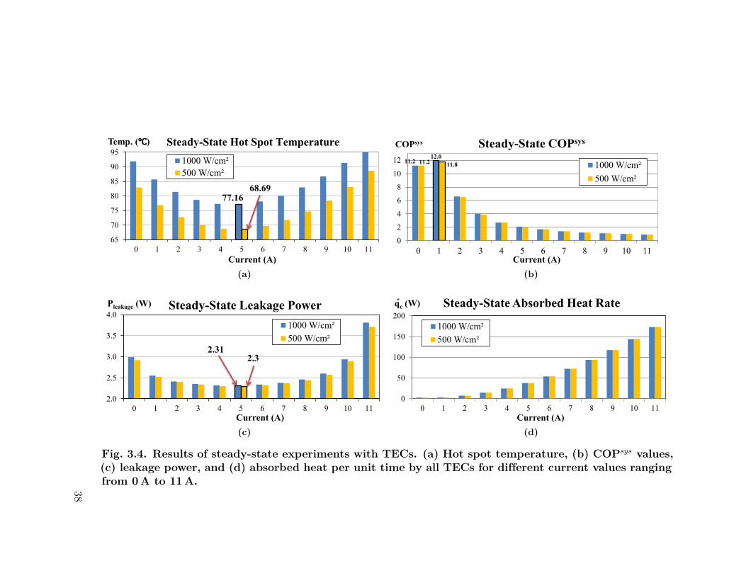
77.1668.69
65
70
75
80
85
90
95
0 1 2 3 4 5 6 7 8 9 10 11
Temp. (℃)
Current (A)
1000 W/cm²500 W/cm²
Steady-State Hot Spot Temperature
(a)
11.212.0
11.2 11.8
0
2
4
6
8
10
12
0 1 2 3 4 5 6 7 8 9 10 11
COPsys
Current (A)
Steady-State COPsys
1000 W/cm²500 W/cm²
(b)
2.312.3
2.0
2.5
3.0
3.5
4.0
0 1 2 3 4 5 6 7 8 9 10 11
Pleakage (W)
Current (A)
Steady-State Leakage Power1000 W/cm²500 W/cm²
(c)
0
50
100
150
200
0 1 2 3 4 5 6 7 8 9 10 11
qc (W)
Current (A)
Steady-State Absorbed Heat Rate
1000 W/cm²500 W/cm²
(d)
Fig. 3.4. Results of steady-state experiments with TECs. (a) Hot spot temperature, (b) COP𝑠𝑦𝑠 values,(c) leakage power, and (d) absorbed heat per unit time by all TECs for different current values rangingfrom 0 A to 11 A.38
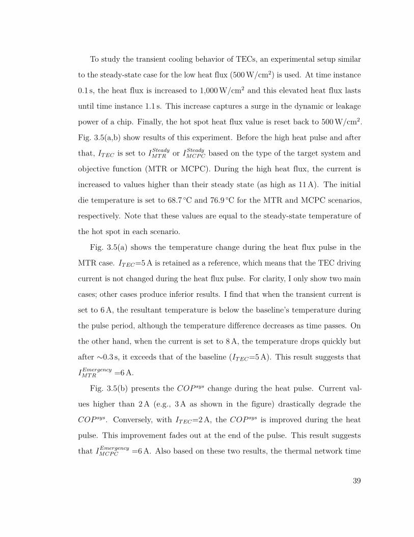
To study the transient cooling behavior of TECs, an experimental setup similar
to the steady-state case for the low heat flux (500 W/cm2) is used. At time instance
0.1 s, the heat flux is increased to 1,000 W/cm2 and this elevated heat flux lasts
until time instance 1.1 s. This increase captures a surge in the dynamic or leakage
power of a chip. Finally, the hot spot heat flux value is reset back to 500 W/cm2.
Fig. 3.5(a,b) show results of this experiment. Before the high heat pulse and after
that, 𝐼𝑇 𝐸𝐶 is set to 𝐼𝑆𝑡𝑒𝑎𝑑𝑦𝑀𝑇 𝑅 or 𝐼𝑆𝑡𝑒𝑎𝑑𝑦
𝑀𝐶𝑃 𝐶 based on the type of the target system and
objective function (MTR or MCPC). During the high heat flux, the current is
increased to values higher than their steady state (as high as 11 A). The initial
die temperature is set to 68.7 ∘C and 76.9 ∘C for the MTR and MCPC scenarios,
respectively. Note that these values are equal to the steady-state temperature of
the hot spot in each scenario.
Fig. 3.5(a) shows the temperature change during the heat flux pulse in the
MTR case. 𝐼𝑇 𝐸𝐶=5 A is retained as a reference, which means that the TEC driving
current is not changed during the heat flux pulse. For clarity, I only show two main
cases; other cases produce inferior results. I find that when the transient current is
set to 6 A, the resultant temperature is below the baseline’s temperature during
the pulse period, although the temperature difference decreases as time passes. On
the other hand, when the current is set to 8 A, the temperature drops quickly but
after ∼0.3 s, it exceeds that of the baseline (𝐼𝑇 𝐸𝐶=5 A). This result suggests that
𝐼𝐸𝑚𝑒𝑟𝑔𝑒𝑛𝑐𝑦𝑀𝑇 𝑅 =6 A.
Fig. 3.5(b) presents the 𝐶𝑂𝑃 𝑠𝑦𝑠 change during the heat pulse. Current val-
ues higher than 2 A (e.g., 3 A as shown in the figure) drastically degrade the
𝐶𝑂𝑃 𝑠𝑦𝑠. Conversely, with 𝐼𝑇 𝐸𝐶=2 A, the 𝐶𝑂𝑃 𝑠𝑦𝑠 is improved during the heat
pulse. This improvement fades out at the end of the pulse. This result suggests
that 𝐼𝐸𝑚𝑒𝑟𝑔𝑒𝑛𝑐𝑦𝑀𝐶𝑃 𝐶 =6 A. Also based on these two results, the thermal network time
39
Time (sec)
0.0 0.5 1.0 1.5
Tem
per
atu
re (°C
)
75
80
85
90Transient Behavior of the Hot Spot Temperature
I=5A
I=6A
I=8A
(a)
Time (sec)
0.0 0.5 1.0 1.5
CO
Psy
s
4.0
4.5
5.0
5.5
6.0
6.5Transient Behavior of the COP
sys
I=1A
I=2A
I=3A
(b)
Fig. 3.5. Results of transient cooling experiments with TECs. (a) Hotspot temperature change and (b) COP𝑠𝑦𝑠 change when applying a one-second heat pulse to the center of the chip to make a hot spot.
constant (𝑇𝑅𝐶) should be set to a value slightly higher than 1 s.
3.5 Summary
This chapter investigated various venues to improve the performance of TECs
embedded inside a processor package. First a new definition for COP of TECs
considering the system’s leakage power dissipation, which is exponentially dependent
on the die temperature, was presented. Next, it was shown that well-tuned TECs
40
in the MCPC mode can improve the COP of an entire cooling system by 7% while
reducing the temperature of chip hot spots by 6 ∘C. Moreover, it was shown that
the TEC driving current that yields the maximum drop in the chip temperature is
quite different from the one that runs the TEC in its highest COP state (5 A vs.
1 A). Finally, a platform-dependent, leakage-aware cooling policy was proposed in
which the TEC driving current was set based on the target platform/application
(i.e., high-performance vs. low-power) and the actual conditions of the chip (i.e.,
emergency vs. preventive thermal management).
41
4Joint Control of Forced-Convection and
Thermoelectric Coolers
4.1 Overview
Both of the heat rejected from hot spots and the heat generated by TECs (as a
result of Joule heating) must be disposed to the ambient; otherwise, the accumulated
heat on the hot side of TECs adversely affects their cooling performance. To achieve
this, standard convention cooling techniques (i.e., natural- and forced-convection
cooling) may be used. The natural-convection cooling method is useful when the
total amount of heat to be disposed is small. On the other hand, the forced-
convection cooling allows more heat to be pumped from the chip using a fan. This
extra ability comes at the cost of increased cooling power consumption. In this
case, the total cooling power of the chip will be equal to the power usage of TECs
and the fan. Moreover, simultaneously controlling the fan and TECs such that
the entire system meets its thermal and power constraints is a challenging task. If
TECs are driven by a high current level and the fan rotation speed is set to be too
low, the rejected heat is trapped between the TEC and the fan, and hence, the
hybrid cooling approach will not be effective. On the other hand, if the driving
current of TECs is set to be too low but the fan rotation speed is set to be high,
42
there is not enough pumped heat for the fan to blow away. Moreover, setting the
fan speed and the TEC driving current to high levels increases the cooling power
consumption, which negatively affects the power efficiency.
The argument presented in the previous paragraph suggests that the TEC
driving current and the fan rotation speed are two interrelated variables which
directly affect the system temperature and the system cooling power consumption.
As a result, there should be an optimum operating point at which the fan and
TECs can work whereby the system thermal constraints is met and the total cooling
power is minimized. In this work, I focus on this joint optimization problem.
To optimize TECs and fans, an accurate study of these devices is necessary.
This study requires a simple, yet accurate, model of a hybrid chip cooling assembly
in order to streamline the problem formulation and ease the process of finding the
solution. An important consideration in this optimization problem is the leakage
power, which is exponentially dependent on the temperature. Investing more power
in the cooling may pay off well as a result of a dramatic power saving in the chip
leakage power consumption. Therefore, the leakage power is considered in the
proposed model and in the formulation.
Key contributions of this chapter are the following:
1. Presenting a compact thermal model for the hybrid chip cooling assembly
comprised of TECs and a fan.
2. Proposing an optimization framework, called OFTEC (Optimization of Forced-
convection and ThermoElectric Coolers), for minimizing the cooling-related
power consumption while adhering a maximum die temperature constraint.
I show that OFTEC can meet the thermal constraints in all of the tested bench-
marks, whereas a system without TECs fails to meet the temperature constraint in
43
five out of eight benchmarks. In the remaining three benchmarks, OFTEC performs
more power efficiently compared to a system without TECs by consuming 5.4%
less power on average while keeping the hottest spot 3.7 ∘C cooler on average. For
all of the eight benchmarks, the average runtime of OFTEC is 437 ms while the
slowest runtime is 693 ms. Moreover, it is shown that a system which adopts TECs
as the only cooling method cannot avoid the thermal runaway situation in these
benchmarks.
The rest of this chapter is organized as follows. Section 4.2 presents thermal
models that are used in this chapter. Next, Section 4.3 explains the problem
formulation and the proposed solution. At the end, Section 4.4 presents experimental
results and Section 4.5 summarizes the chapter.
4.2 Modeling
I use the duality between electrical and thermal phenomena to make a circuit
model of a cooling package similar to the one presented in Fig. 2.3. In this model,
each physical component is decomposed into several sub-components. Increasing
the number of these sub-components increases the accuracy of the model; however,
it also increases the complexity of the electrical circuit model, and thus, makes the
analysis slow.
The processor package is comprised of eight layers:
1. PCB 2. chip 3. TIM1 4. TEC
5. heat spreader 6. TIM2 7. heat sink 8. fan
Layers 1, 3, 5, and 6 are denoted by 𝐿𝑐𝑜𝑛𝑑𝑢𝑐𝑡 in this work. Sub-components in
𝐿𝑐𝑜𝑛𝑑𝑢𝑐𝑡 only conduct heat (i.e., they do not generate or absorb heat). Therefore,
44
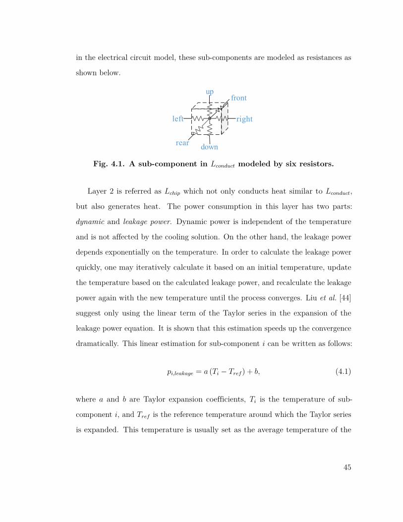
in the electrical circuit model, these sub-components are modeled as resistances as
shown below.
up
down
left right
front
rear
Fig. 4.1. A sub-component in 𝐿𝑐𝑜𝑛𝑑𝑢𝑐𝑡 modeled by six resistors.
Layer 2 is referred as 𝐿𝑐ℎ𝑖𝑝 which not only conducts heat similar to 𝐿𝑐𝑜𝑛𝑑𝑢𝑐𝑡,
but also generates heat. The power consumption in this layer has two parts:
dynamic and leakage power. Dynamic power is independent of the temperature
and is not affected by the cooling solution. On the other hand, the leakage power
depends exponentially on the temperature. In order to calculate the leakage power
quickly, one may iteratively calculate it based on an initial temperature, update
the temperature based on the calculated leakage power, and recalculate the leakage
power again with the new temperature until the process converges. Liu et al. [44]
suggest only using the linear term of the Taylor series in the expansion of the
leakage power equation. It is shown that this estimation speeds up the convergence
dramatically. This linear estimation for sub-component 𝑖 can be written as follows:
𝑝𝑖,𝑙𝑒𝑎𝑘𝑎𝑔𝑒 = 𝑎 (𝑇𝑖 − 𝑇𝑟𝑒𝑓 ) + 𝑏, (4.1)
where 𝑎 and 𝑏 are Taylor expansion coefficients, 𝑇𝑖 is the temperature of sub-
component 𝑖, and 𝑇𝑟𝑒𝑓 is the reference temperature around which the Taylor series
is expanded. This temperature is usually set as the average temperature of the
45
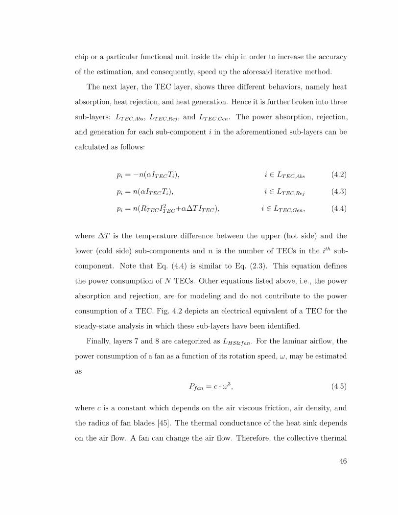
chip or a particular functional unit inside the chip in order to increase the accuracy
of the estimation, and consequently, speed up the aforesaid iterative method.
The next layer, the TEC layer, shows three different behaviors, namely heat
absorption, heat rejection, and heat generation. Hence it is further broken into three
sub-layers: 𝐿𝑇 𝐸𝐶,𝐴𝑏𝑠, 𝐿𝑇 𝐸𝐶,𝑅𝑒𝑗, and 𝐿𝑇 𝐸𝐶,𝐺𝑒𝑛. The power absorption, rejection,
and generation for each sub-component 𝑖 in the aforementioned sub-layers can be
calculated as follows:
𝑝𝑖 = −𝑛(𝛼𝐼𝑇 𝐸𝐶𝑇𝑖), 𝑖 ∈ 𝐿𝑇 𝐸𝐶,𝐴𝑏𝑠 (4.2)
𝑝𝑖 = 𝑛(𝛼𝐼𝑇 𝐸𝐶𝑇𝑖), 𝑖 ∈ 𝐿𝑇 𝐸𝐶,𝑅𝑒𝑗 (4.3)
𝑝𝑖 = 𝑛(𝑅𝑇 𝐸𝐶𝐼2𝑇 𝐸𝐶+𝛼Δ𝑇𝐼𝑇 𝐸𝐶), 𝑖 ∈ 𝐿𝑇 𝐸𝐶,𝐺𝑒𝑛, (4.4)
where Δ𝑇 is the temperature difference between the upper (hot side) and the
lower (cold side) sub-components and 𝑛 is the number of TECs in the 𝑖𝑡ℎ sub-
component. Note that Eq. (4.4) is similar to Eq. (2.3). This equation defines
the power consumption of 𝑁 TECs. Other equations listed above, i.e., the power
absorption and rejection, are for modeling and do not contribute to the power
consumption of a TEC. Fig. 4.2 depicts an electrical equivalent of a TEC for the
steady-state analysis in which these sub-layers have been identified.
Finally, layers 7 and 8 are categorized as 𝐿𝐻𝑆&𝑓𝑎𝑛. For the laminar airflow, the
power consumption of a fan as a function of its rotation speed, 𝜔, may be estimated
as
𝑃𝑓𝑎𝑛 = 𝑐 · 𝜔3, (4.5)
where 𝑐 is a constant which depends on the air viscous friction, air density, and
the radius of fan blades [45]. The thermal conductance of the heat sink depends
on the air flow. A fan can change the air flow. Therefore, the collective thermal
46
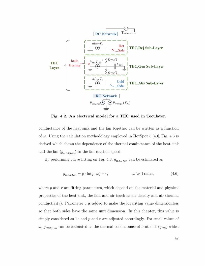
KTEC/2
KTEC/2RTECITEC2
-αITECTc
αITECTh
TEC,Gen Sub-Layer
TEC,Abs Sub-Layer
TEC,Rej Sub-Layer
CTEC
RC Network Tambient
Pleakage (Tdie)
RC Network
Pdynamic
TEC Layer
Fig. 4.2. An electrical model for a TEC used in Teculator.
conductance of the heat sink and the fan together can be written as a function
of 𝜔. Using the calculation methodology employed in HotSpot 5 [40], Fig. 4.3 is
derived which shows the dependence of the thermal conductance of the heat sink
and the fan (𝑔𝐻𝑆&𝑓𝑎𝑛) to the fan rotation speed.
By performing curve fitting on Fig. 4.3, 𝑔𝐻𝑆&𝑓𝑎𝑛 can be estimated as
𝑔𝐻𝑆&𝑓𝑎𝑛 = 𝑝 · ln(𝑞 · 𝜔) + 𝑟, 𝜔 ≫ 1 rad/s, (4.6)
where 𝑝 and 𝑟 are fitting parameters, which depend on the material and physical
properties of the heat sink, the fan, and air (such as air density and air thermal
conductivity). Parameter 𝑞 is added to make the logarithm value dimensionless
so that both sides have the same unit dimension. In this chapter, this value is
simply considered as 1 s and 𝑝 and 𝑟 are adjusted accordingly. For small values of
𝜔, 𝑔𝐻𝑆&𝑓𝑎𝑛 can be estimated as the thermal conductance of heat sink (𝑔𝐻𝑆) which
47
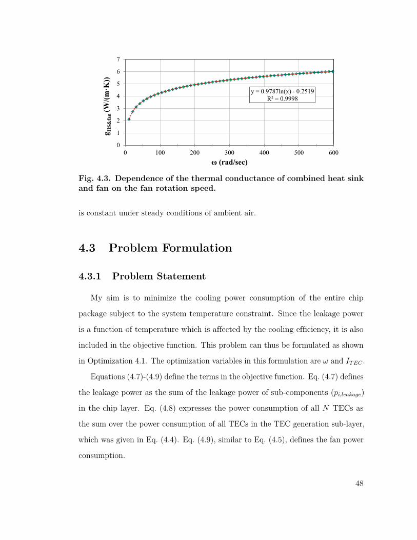
y = 0.9787ln(x) - 0.2519R² = 0.9998
0
1
2
3
4
5
6
7
0 100 200 300 400 500 600
g HS&
fan
(W/(m
·K))
ω (rad/sec)
Fig. 4.3. Dependence of the thermal conductance of combined heat sinkand fan on the fan rotation speed.
is constant under steady conditions of ambient air.
4.3 Problem Formulation
4.3.1 Problem Statement
My aim is to minimize the cooling power consumption of the entire chip
package subject to the system temperature constraint. Since the leakage power
is a function of temperature which is affected by the cooling efficiency, it is also
included in the objective function. This problem can thus be formulated as shown
in Optimization 4.1. The optimization variables in this formulation are 𝜔 and 𝐼𝑇 𝐸𝐶 .
Equations (4.7)-(4.9) define the terms in the objective function. Eq. (4.7) defines
the leakage power as the sum of the leakage power of sub-components (𝑝𝑖,𝑙𝑒𝑎𝑘𝑎𝑔𝑒)
in the chip layer. Eq. (4.8) expresses the power consumption of all 𝑁 TECs as
the sum over the power consumption of all TECs in the TEC generation sub-layer,
which was given in Eq. (4.4). Eq. (4.9), similar to Eq. (4.5), defines the fan power
consumption.
48
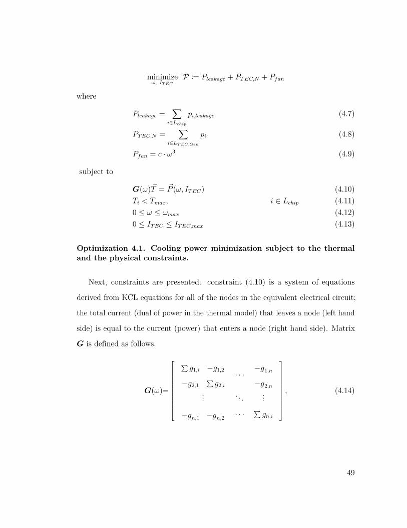
minimize𝜔, 𝐼𝑇 𝐸𝐶
𝒫 := 𝑃𝑙𝑒𝑎𝑘𝑎𝑔𝑒 + 𝑃𝑇 𝐸𝐶,𝑁 + 𝑃𝑓𝑎𝑛
where
𝑃𝑙𝑒𝑎𝑘𝑎𝑔𝑒 =∑︁
𝑖∈𝐿𝑐ℎ𝑖𝑝
𝑝𝑖,𝑙𝑒𝑎𝑘𝑎𝑔𝑒 (4.7)
𝑃𝑇 𝐸𝐶,𝑁 =∑︁
𝑖∈𝐿𝑇 𝐸𝐶,𝐺𝑒𝑛
𝑝𝑖 (4.8)
𝑃𝑓𝑎𝑛 = 𝑐 · 𝜔3 (4.9)
subject to
𝐺(𝜔)𝑇 = 𝑃 (𝜔, 𝐼𝑇 𝐸𝐶) (4.10)𝑇𝑖 < 𝑇𝑚𝑎𝑥, 𝑖 ∈ 𝐿𝑐ℎ𝑖𝑝 (4.11)0 ≤ 𝜔 ≤ 𝜔𝑚𝑎𝑥 (4.12)0 ≤ 𝐼𝑇 𝐸𝐶 ≤ 𝐼𝑇 𝐸𝐶,𝑚𝑎𝑥 (4.13)
Optimization 4.1. Cooling power minimization subject to the thermaland the physical constraints.
Next, constraints are presented. constraint (4.10) is a system of equations
derived from KCL equations for all of the nodes in the equivalent electrical circuit;
the total current (dual of power in the thermal model) that leaves a node (left hand
side) is equal to the current (power) that enters a node (right hand side). Matrix
𝐺 is defined as follows.
𝐺(𝜔)=
⎡⎢⎢⎢⎢⎢⎢⎢⎢⎢⎣
∑︀𝑔1,𝑖 −𝑔1,2
−𝑔2,1∑︀
𝑔2,𝑖
· · ·−𝑔1,𝑛
−𝑔2,𝑛
... . . . ...
−𝑔𝑛,1 −𝑔𝑛,2 · · · ∑︀𝑔𝑛,𝑖
⎤⎥⎥⎥⎥⎥⎥⎥⎥⎥⎦, (4.14)
49
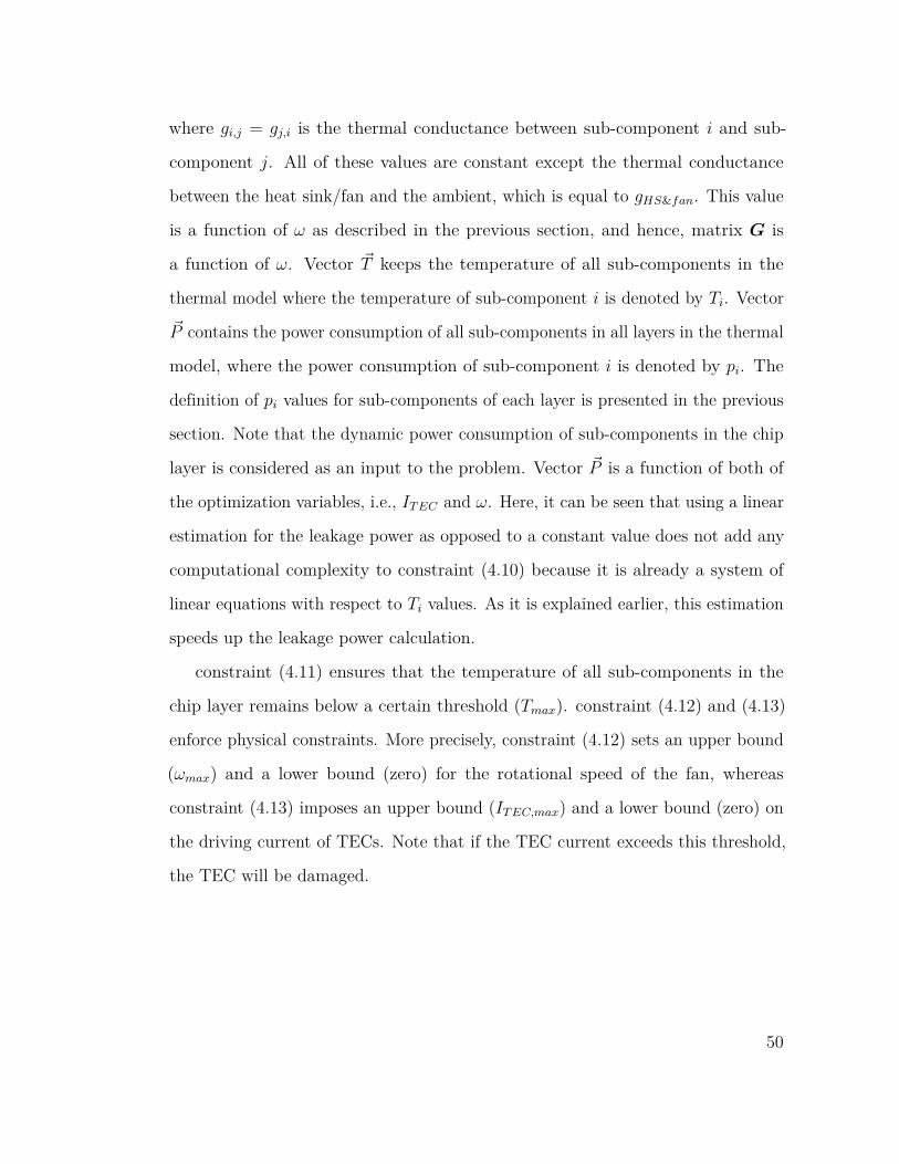
where 𝑔𝑖,𝑗 = 𝑔𝑗,𝑖 is the thermal conductance between sub-component 𝑖 and sub-
component 𝑗. All of these values are constant except the thermal conductance
between the heat sink/fan and the ambient, which is equal to 𝑔𝐻𝑆&𝑓𝑎𝑛. This value
is a function of 𝜔 as described in the previous section, and hence, matrix 𝐺 is
a function of 𝜔. Vector 𝑇 keeps the temperature of all sub-components in the
thermal model where the temperature of sub-component 𝑖 is denoted by 𝑇𝑖. Vector
𝑃 contains the power consumption of all sub-components in all layers in the thermal
model, where the power consumption of sub-component 𝑖 is denoted by 𝑝𝑖. The
definition of 𝑝𝑖 values for sub-components of each layer is presented in the previous
section. Note that the dynamic power consumption of sub-components in the chip
layer is considered as an input to the problem. Vector 𝑃 is a function of both of
the optimization variables, i.e., 𝐼𝑇 𝐸𝐶 and 𝜔. Here, it can be seen that using a linear
estimation for the leakage power as opposed to a constant value does not add any
computational complexity to constraint (4.10) because it is already a system of
linear equations with respect to 𝑇𝑖 values. As it is explained earlier, this estimation
speeds up the leakage power calculation.
constraint (4.11) ensures that the temperature of all sub-components in the
chip layer remains below a certain threshold (𝑇𝑚𝑎𝑥). constraint (4.12) and (4.13)
enforce physical constraints. More precisely, constraint (4.12) sets an upper bound
(𝜔𝑚𝑎𝑥) and a lower bound (zero) for the rotational speed of the fan, whereas
constraint (4.13) imposes an upper bound (𝐼𝑇 𝐸𝐶,𝑚𝑎𝑥) and a lower bound (zero) on
the driving current of TECs. Note that if the TEC current exceeds this threshold,
the TEC will be damaged.
50
4.3.2 Proposed Solution
The problem formulation presented in Optimization 4.1 is not convex. Moreover,
due to the iterations required for the calculation of leakage power, the objective
function 𝒫 can only be determined numerically for a given 𝜔 and 𝐼𝑇 𝐸𝐶 . This problem
is classified as a constrained nonlinear program (CNLP). I experimented with three
state-of-the-art nonlinear optimization techniques for solving this problem, namely,
interior-point method, trust-region technique, and active-set sequential quadratic
programming (SQP) method [46]. It turns out that the last technique, i.e., the
active-set SQP method performs the best for the formulation both in terms of
solution quality and speed. This technique is briefly explained next.
The active-set SQP tries to find a solution for Karush-Kuhn-Tucker (KKT)
conditions, which are necessary conditions for the optimality of a solution. At any
optimum point, when a constraint is active, its contour is tangential to that of
the objective function. This means that the gradient of the objective function is
equal to the gradient of the active constraint, though it may have different absolute
value. Lagrangian multipliers are used to compensate for different gradient sizes.
These multipliers are non-zero when a non-equality constraint is active and zero
otherwise. The active-set SQP method tries to solve the KKT conditions iteratively
by approximating those using convex quadratic programs (QPs). Solving QPs
allows determining the search direction. Having the search direction and the step
length (which can be found through a line search method), a near-optimal solution
can be found. Since the non-convexity of the optimization function of interest is
minor (this will be shown later in experimental results), the active-set SQP method
produces high quality results very quickly. A detailed explanation of the active-set
SQP method can be found in [46].
The active-set SQP method, similar to other nonlinear optimization techniques,
51
requires an initial feasible solution. Finding an initial solution is not trivial since
the relation between constraint (4.11) and optimization variables is set by the set of
nonlinear equations listed in constraint (4.10). On the other hand, minimization of
the objective function irrespective of the constraints may violate constraint (4.11).
To address this difficulty, a new optimization problem is formulated in order to
find an initial feasible solution for the original problem. The formulation is listed
below. In this optimization problem, similar to the previous one, the optimization
variables are 𝜔 and 𝐼𝑇 𝐸𝐶 .
minimize𝜔,𝐼𝑇 𝐸𝐶
𝒯 := max𝑖∈𝐿𝑐ℎ𝑖𝑝{𝑇 𝑖}
subject to
𝐺(𝜔)𝑇 = 𝑃 (𝜔, 𝐼𝑇 𝐸𝐶) (4.15)0 ≤ 𝜔 ≤ 𝜔𝑚𝑎𝑥 (4.16)0 ≤ 𝐼𝑇 𝐸𝐶 ≤ 𝐼𝑇 𝐸𝐶,𝑚𝑎𝑥 (4.17)
Optimization 4.2. Minimizing the maximum chip temperature subjectto the thermal and the physical constraints.
Finding an initial solution for this problem is trivial; it can be done by arbitrarily
selecting (𝜔, 𝐼𝑇 𝐸𝐶) such that the pair satisfies domain constraints (4.16) and (4.17).
In this work, I set these initial values as (𝜔𝑚𝑎𝑥
2 ,𝐼𝑇 𝐸𝐶,𝑚𝑎𝑥
2 ). This assumption does not
violate constraint (4.15) because 𝑇𝑖’s will be adjusted accordingly. Optimization 4.2
is an interesting problem by itself since it minimizes the maximum die temperature,
which leads to the minimization of the maximum leakage power and also it slows
down the aging rate of the sub-component on the chip layer with the highest
temperature. So this solution has its own applications as long as the cooling power
consumption is not a concern. If it turns out that the minimized max𝑖∈𝐿𝑐ℎ𝑖𝑝{𝑇 𝑖}
52
is greater than 𝑇𝑚𝑎𝑥, it can be concluded that Optimization 4.1 has no solution,
i.e., it is infeasible. Moreover, the solver can stop the optimization procedure as
soon as it finds the first solution which makes max𝑖∈𝐿𝑐ℎ𝑖𝑝{𝑇 𝑖} smaller than 𝑇𝑚𝑎𝑥.
Having an initial feasible solution for Optimization 4.1, one can use the active-set
SQP method to approximately solve it. Algorithm 4.1, which is called optimization
of forced-convection and thermoelectric coolers (OFTEC), presents this approach.
Algorithm 4.1. OFTECInput: Physical characteristics of the cooling package and the dynamic powerconsumption of each sub-component in the chip layer.Output: 𝜔* and 𝐼*
𝑇 𝐸𝐶
1: (𝜔0, 𝐼𝑇 𝐸𝐶,0)← (𝜔max2 ,
𝐼𝑇 𝐸𝐶,𝑚𝑎𝑥
2 )2: if 𝒯 (𝜔1, 𝐼𝑇 𝐸𝐶,1) > 𝑇𝑚𝑎𝑥 then3: (𝜔1, 𝐼𝑇 𝐸𝐶,1) ←Call the active-set SQP method to solve Optimization 4.2
with the initial solution (𝜔0, 𝐼𝑇 𝐸𝐶,0). Stop the optimization whenever𝒯 (𝜔,𝐼TEC)<𝑇𝑚𝑎𝑥.
4: if 𝒯 (𝜔1, 𝐼𝑇 𝐸𝐶,1) > 𝑇𝑚𝑎𝑥 then5: return failed // no solution is found6: end if7: end if8: (𝜔*, 𝐼*
𝑇 𝐸𝐶)←Call the active-set SQP method to solve Optimization 4.1 withthe initial solution (𝜔1, 𝐼𝑇 𝐸𝐶,1).
9: return (𝜔*, 𝐼*𝑇 𝐸𝐶)
4.4 Experimental Results
4.4.1 Simulation Setup
In order to evaluate OFTEC, the flow shown in Fig. 4.4 is developed. The
experiments target the Alpha 21264 processor. PTscalar [47] is used as the perfor-
mance/power simulator in order to generate the dynamic power trace for benchmarks
which are selected from the MiBench benchmark suite [48]. The maximum power
consumption for each sub-component in the chip layer is selected to be passed to
53
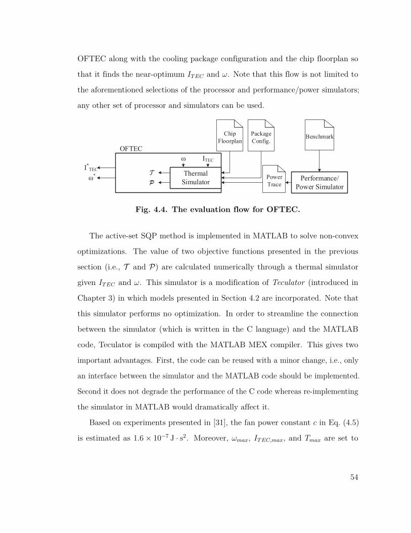
OFTEC along with the cooling package configuration and the chip floorplan so
that it finds the near-optimum 𝐼𝑇 𝐸𝐶 and 𝜔. Note that this flow is not limited to
the aforementioned selections of the processor and performance/power simulators;
any other set of processor and simulators can be used.
OFTEC
P
I*TEC
ω*
BenchmarkChip Floorplan
Performance/Power Simulator
Power Trace
Thermal Simulator
Package Config.
ITECω
Fig. 4.4. The evaluation flow for OFTEC.
The active-set SQP method is implemented in MATLAB to solve non-convex
optimizations. The value of two objective functions presented in the previous
section (i.e., 𝒯 and 𝒫) are calculated numerically through a thermal simulator
given 𝐼𝑇 𝐸𝐶 and 𝜔. This simulator is a modification of Teculator (introduced in
Chapter 3) in which models presented in Section 4.2 are incorporated. Note that
this simulator performs no optimization. In order to streamline the connection
between the simulator (which is written in the C language) and the MATLAB
code, Teculator is compiled with the MATLAB MEX compiler. This gives two
important advantages. First, the code can be reused with a minor change, i.e., only
an interface between the simulator and the MATLAB code should be implemented.
Second it does not degrade the performance of the C code whereas re-implementing
the simulator in MATLAB would dramatically affect it.
Based on experiments presented in [31], the fan power constant 𝑐 in Eq. (4.5)
is estimated as 1.6× 10⁻⁷ J · s2. Moreover, 𝜔𝑚𝑎𝑥, 𝐼𝑇 𝐸𝐶,𝑚𝑎𝑥, and 𝑇𝑚𝑎𝑥 are set to
54
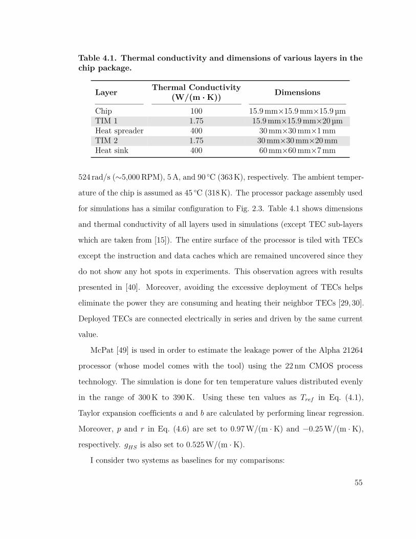
Table 4.1. Thermal conductivity and dimensions of various layers in thechip package.
Layer Thermal Conductivity(W/(m · K)) Dimensions
Chip 100 15.9 mm×15.9 mm×15.9 µmTIM 1 1.75 15.9 mm×15.9 mm×20 µmHeat spreader 400 30 mm×30 mm×1 mmTIM 2 1.75 30 mm×30 mm×20 mmHeat sink 400 60 mm×60 mm×7 mm
524 rad/s (∼5,000 RPM), 5 A, and 90 ∘C (363 K), respectively. The ambient temper-
ature of the chip is assumed as 45 ∘C (318 K). The processor package assembly used
for simulations has a similar configuration to Fig. 2.3. Table 4.1 shows dimensions
and thermal conductivity of all layers used in simulations (except TEC sub-layers
which are taken from [15]). The entire surface of the processor is tiled with TECs
except the instruction and data caches which are remained uncovered since they
do not show any hot spots in experiments. This observation agrees with results
presented in [40]. Moreover, avoiding the excessive deployment of TECs helps
eliminate the power they are consuming and heating their neighbor TECs [29,30].
Deployed TECs are connected electrically in series and driven by the same current
value.
McPat [49] is used in order to estimate the leakage power of the Alpha 21264
processor (whose model comes with the tool) using the 22 nm CMOS process
technology. The simulation is done for ten temperature values distributed evenly
in the range of 300 K to 390 K. Using these ten values as 𝑇𝑟𝑒𝑓 in Eq. (4.1),
Taylor expansion coefficients 𝑎 and 𝑏 are calculated by performing linear regression.
Moreover, 𝑝 and 𝑟 in Eq. (4.6) are set to 0.97 W/(m ·K) and −0.25 W/(m ·K),
respectively. 𝑔𝐻𝑆 is also set to 0.525 W/(m ·K).
I consider two systems as baselines for my comparisons:
55
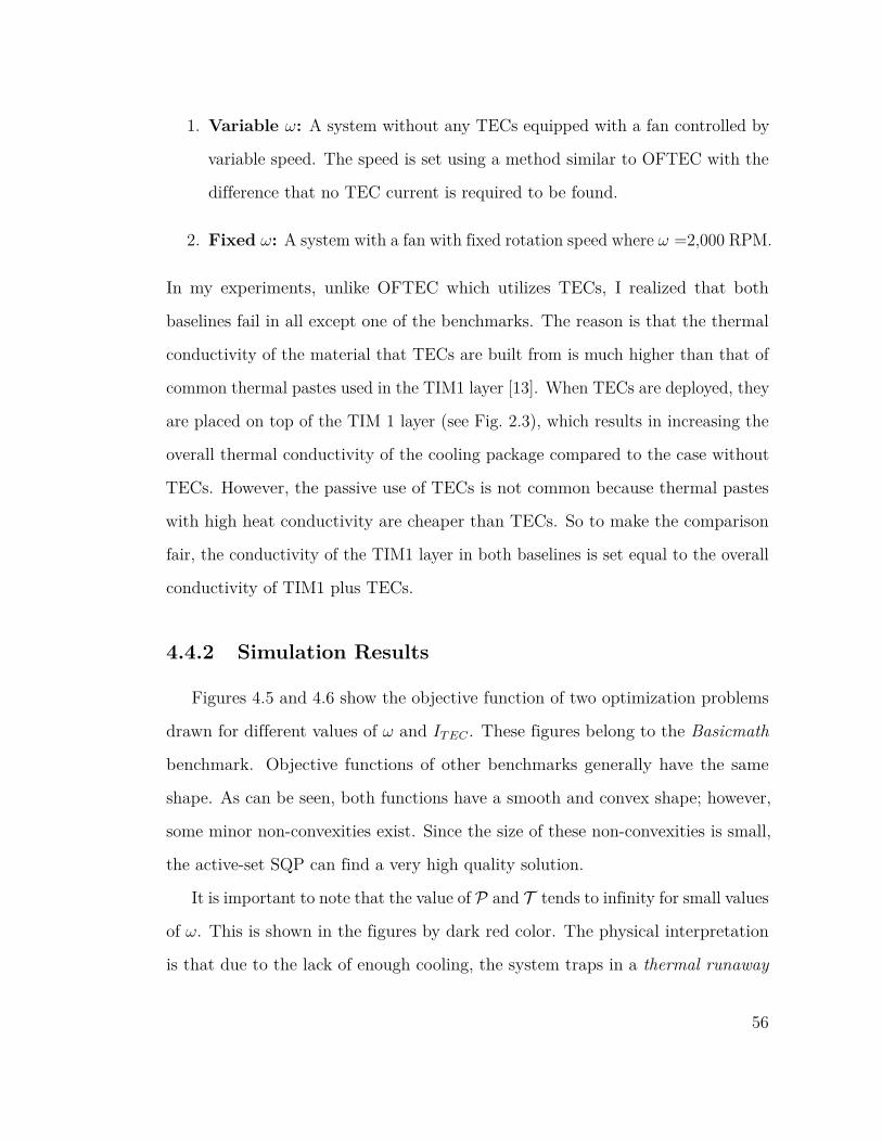
1. Variable 𝜔: A system without any TECs equipped with a fan controlled by
variable speed. The speed is set using a method similar to OFTEC with the
difference that no TEC current is required to be found.
2. Fixed 𝜔: A system with a fan with fixed rotation speed where 𝜔 =2,000 RPM.
In my experiments, unlike OFTEC which utilizes TECs, I realized that both
baselines fail in all except one of the benchmarks. The reason is that the thermal
conductivity of the material that TECs are built from is much higher than that of
common thermal pastes used in the TIM1 layer [13]. When TECs are deployed, they
are placed on top of the TIM 1 layer (see Fig. 2.3), which results in increasing the
overall thermal conductivity of the cooling package compared to the case without
TECs. However, the passive use of TECs is not common because thermal pastes
with high heat conductivity are cheaper than TECs. So to make the comparison
fair, the conductivity of the TIM1 layer in both baselines is set equal to the overall
conductivity of TIM1 plus TECs.
4.4.2 Simulation Results
Figures 4.5 and 4.6 show the objective function of two optimization problems
drawn for different values of 𝜔 and 𝐼𝑇 𝐸𝐶 . These figures belong to the Basicmath
benchmark. Objective functions of other benchmarks generally have the same
shape. As can be seen, both functions have a smooth and convex shape; however,
some minor non-convexities exist. Since the size of these non-convexities is small,
the active-set SQP can find a very high quality solution.
It is important to note that the value of 𝒫 and 𝒯 tends to infinity for small values
of 𝜔. This is shown in the figures by dark red color. The physical interpretation
is that due to the lack of enough cooling, the system traps in a thermal runaway
56
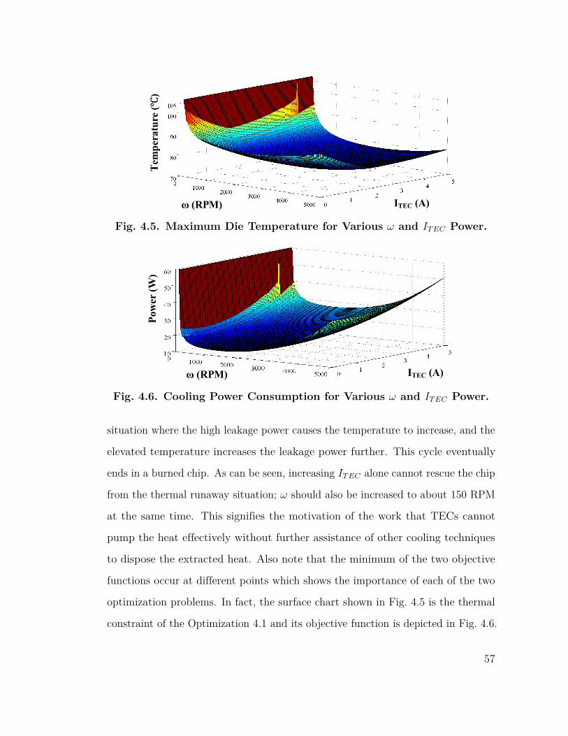
ITEC (A) ω (RPM)
Tem
pera
ture
(℃)
Fig. 4.5. Maximum Die Temperature for Various 𝜔 and 𝐼𝑇 𝐸𝐶 Power.
ITEC (A) ω (RPM)
Pow
er (W
)
Fig. 4.6. Cooling Power Consumption for Various 𝜔 and 𝐼𝑇 𝐸𝐶 Power.
situation where the high leakage power causes the temperature to increase, and the
elevated temperature increases the leakage power further. This cycle eventually
ends in a burned chip. As can be seen, increasing 𝐼𝑇 𝐸𝐶 alone cannot rescue the chip
from the thermal runaway situation; 𝜔 should also be increased to about 150 RPM
at the same time. This signifies the motivation of the work that TECs cannot
pump the heat effectively without further assistance of other cooling techniques
to dispose the extracted heat. Also note that the minimum of the two objective
functions occur at different points which shows the importance of each of the two
optimization problems. In fact, the surface chart shown in Fig. 4.5 is the thermal
constraint of the Optimization 4.1 and its objective function is depicted in Fig. 4.6.
57
In Fig. 4.5, the minimum occurs at almost the middle of the (𝜔-𝐼𝑇 𝐸𝐶) plane. That
is why in the first line of Algorithm 4.1, I set the initial value of (𝜔, 𝐼𝑇 𝐸𝐶) as
(𝜔𝑚𝑎𝑥
2 ,𝐼𝑇 𝐸𝐶,𝑚𝑎𝑥
2 ). Further increase of 𝜔 and 𝐼𝑇 𝐸𝐶 values causes more heat to be
generated by the fan and TECs than the cooling they provide. On the other hand,
in Fig. 4.6, the minimum occurs near the origin.
Figures 4.7 and 4.8 show the results of performing Optimization 2 (i.e., line 3
in Algorithm 4.1). Fig. 4.7 depicts the maximum die temperature (𝒯 ) achieved by
OFTEC and two baselines. The thermal threshold (𝑇𝑚𝑎𝑥) is shown by a dashed
line in this figure. As can be seen, OFTEC could meet the thermal constraint
in all benchmarks, whereas two baselines failed to cool down the system in five
benchmarks which are identified by a red dashed box. These five cases should be
further cooled down using other thermal management techniques such as reducing
the voltage/frequency of the chip or throttling different functional units which leads
to performance degradation. Moreover, on average, OFTEC could achieve more
than 13 ∘C lower temperature compared to the other two cases. Fig. 4.8 compares
the power consumption of these three methods. As can be seen, OFTEC has the
highest power consumption when the objective function is the minimization of the
maximum temperature. This extra power is consumed mostly by TECs.
Figures 4.9 and 4.10 show the results of performing Optimization 4.1. Results
of two baselines are omitted in five benchmarks since they could not meet thermal
constraints and hence do not provide meaningful results. In Optimization 4.1,
OFTEC addresses the trade-off between the cooling power consumption and the
maximum chip temperature. Fig. 4.9 shows that OFTEC slightly increases the
temperature in order to reduce the cooling power consumption. This increase is
done such that the system temperature still meets thermal constraints. Fig. 4.9
compares the power consumption of these three methods. OFTEC has the minimum
58
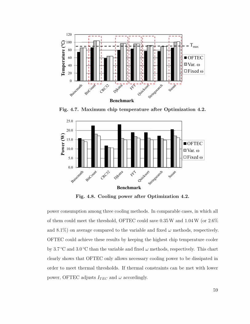
0
20
40
60
80
100
120
Tem
pera
ture
()
Benchmark
OFTECVar. ωFixed ω
Tmax
Fig. 4.7. Maximum chip temperature after Optimization 4.2.
0.0
5.0
10.0
15.0
20.0
25.0
Pow
er (W
)
Benchmark
OFTECVar. ωFixed ω
Fig. 4.8. Cooling power after Optimization 4.2.
power consumption among three cooling methods. In comparable cases, in which all
of them could meet the threshold, OFTEC could save 0.35 W and 1.04 W (or 2.6%
and 8.1%) on average compared to the variable and fixed 𝜔 methods, respectively.
OFTEC could achieve these results by keeping the highest chip temperature cooler
by 3.7 ∘C and 3.0 ∘C than the variable and fixed 𝜔 methods, respectively. This chart
clearly shows that OFTEC only allows necessary cooling power to be dissipated in
order to meet thermal thresholds. If thermal constraints can be met with lower
power, OFTEC adjusts 𝐼𝑇 𝐸𝐶 and 𝜔 accordingly.
59
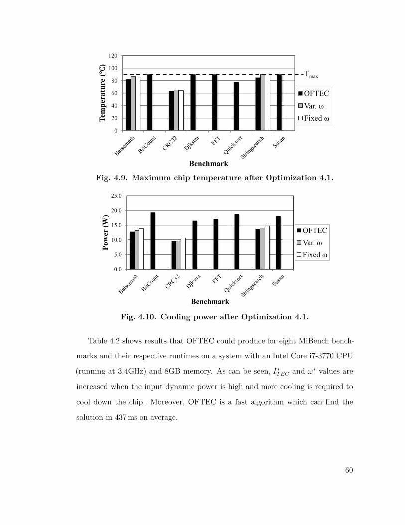
0
20
40
60
80
100
120
Tem
pera
ture
()
Benchmark
OFTECVar. ωFixed ω
Tmax
Fig. 4.9. Maximum chip temperature after Optimization 4.1.
0.0
5.0
10.0
15.0
20.0
25.0
Pow
er (W
)
Benchmark
OFTECVar. ωFixed ω
Fig. 4.10. Cooling power after Optimization 4.1.
Table 4.2 shows results that OFTEC could produce for eight MiBench bench-
marks and their respective runtimes on a system with an Intel Core i7-3770 CPU
(running at 3.4GHz) and 8GB memory. As can be seen, 𝐼*𝑇 𝐸𝐶 and 𝜔* values are
increased when the input dynamic power is high and more cooling is required to
cool down the chip. Moreover, OFTEC is a fast algorithm which can find the
solution in 437 ms on average.
60
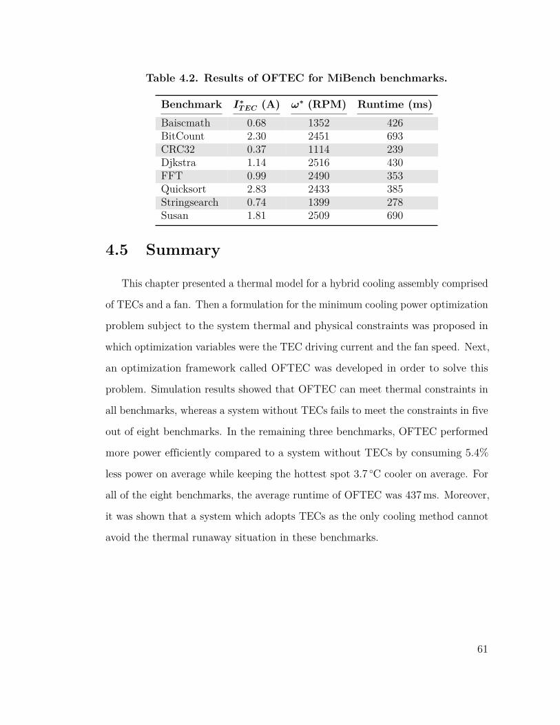
Table 4.2. Results of OFTEC for MiBench benchmarks.
Benchmark 𝐼*𝑇 𝐸𝐶 (A) 𝜔* (RPM) Runtime (ms)
Baiscmath 0.68 1352 426BitCount 2.30 2451 693CRC32 0.37 1114 239Djkstra 1.14 2516 430FFT 0.99 2490 353Quicksort 2.83 2433 385Stringsearch 0.74 1399 278Susan 1.81 2509 690
4.5 Summary
This chapter presented a thermal model for a hybrid cooling assembly comprised
of TECs and a fan. Then a formulation for the minimum cooling power optimization
problem subject to the system thermal and physical constraints was proposed in
which optimization variables were the TEC driving current and the fan speed. Next,
an optimization framework called OFTEC was developed in order to solve this
problem. Simulation results showed that OFTEC can meet thermal constraints in
all benchmarks, whereas a system without TECs fails to meet the constraints in five
out of eight benchmarks. In the remaining three benchmarks, OFTEC performed
more power efficiently compared to a system without TECs by consuming 5.4%
less power on average while keeping the hottest spot 3.7 ∘C cooler on average. For
all of the eight benchmarks, the average runtime of OFTEC was 437 ms. Moreover,
it was shown that a system which adopts TECs as the only cooling method cannot
avoid the thermal runaway situation in these benchmarks.
61
5Fine-Grained Control of Thermoelectric
Coolers Using Bypass Switches
5.1 Overview
Due to the Joule heating effect, the utilization of TECs should be limited to
the time that their associated hot spot is active (i.e., the hot spot temperature
is above the set point). One common approach is to selectively deploy TECs in
order to only cover hot spots on the die (as opposed to covering the entire die) [29].
However, hot spots not only have spatially non-uniform distribution [50], but also
have temporally non-uniform scattering throughout the die [51]. This temporal
non-uniform distribution is due to the fact that each application (or execution
phase of an application) utilizes different functional units on the die and hence
exhibits different set of hot spots.
This chapter aims to minimize the power consumption of TECs by identifying
temporal and spatial distribution of hot spots in a chip, and subsequently, turning
on/off groups of TECs as needed. In traditional designs, TECs are connected
electrically in series, which makes their selective control impossible [12,13,21]. I
propose adding bypass switches in order to allow independent control of TECs.
62
Note that bypass switches are not ideal and have an on-resistance comparable to
that of a single TEC. Hence, they consume power when current flows through them.
Besides, excessive use of bypass switches increases the cost of the cooling system.
Thus, there is a trade-off between the number of switches and the power saving
provided by this approach.
To address this challenge, adjacent hot spots with the exactly same thermal
behavior may be grouped and cooled by a few nearby TECs. I refer to these
TECs as a TEC group. Consequently, each TEC group based on their distance
from each other and the temporal behavior of these hot spots can be controlled
by a single switch. More precisely, I formulate a clustering problem as an integer-
quadratic program that minimizes the wasted power consumption of TECs and
bypass switches. This problem has many variables which makes it impossible to be
solved directly. Hence, I introduce a greedy heuristic to solve the clustering problem.
This heuristic is executed during the design of the cooling system. Subsequently,
during the runtime of the system, if at least a hot spot corresponding to a cluster is
present, the bypass switch of that cluster should be off (does not bypass). Otherwise,
the switch should be on (bypasses). It is shown that the suggested heuristic can
reduce the wasted power on average by 81% and also decrease the total TEC power
consumption on average by 42%.
The rest of this chapter is organized as follows. Section 5.2 introduces a control
circuit for selective control of TEC clusters. Section 5.3 formulates a clustering
problem to minimize the wasted cooling power consumption. Then it presents a
greedy heuristic for clustering TECs. Section 5.4 presents experimental results.
Finally, Section 5.5 summarizes the chapter.
63
5.2 Selective Control of TECs
Various applications (or execution phases of an application) may stress different
functional units of a multi-processor system-on-chip (MPSoC), such as register file,
ALU, and so on. This results in a non-uniform temporal distribution of hot spots
on the chip. As it is explained previously, the common practice for deploying TECs
is to only consider the spatial distribution of TECs by running a set of applications
on the target chip and identifying hot spots accordingly. Next, one or several TECs
are assigned to each hot spot [29].
TECs are often connected in series. This requirement tends to result in a vast
amount of power loss due to the fact that all TECs should remain on as long
as even one hot spot on the chip is present. The reason for serially connecting
TECs is as follows. A TEC can tolerate at most 60 mV voltage difference across its
two terminals while allowing 5 A or more current to pass through it [14]. Hence,
connecting tens or hundreds of TECs in parallel requires hundreds to thousands
of Ampers to be supplied by the current source while maintaining the voltage
difference at tens of millivolts. Clearly, this is not possible, and thus, TECs are
connected serially so that the overall current remains low and the controlling voltage
across the input terminal of the first TEC in the chain and the output terminal of
the last TEC in that chain is large enough so that it can be simply maintained.
Assume that 𝑁 𝑡𝑜𝑡𝑎𝑙𝑇 𝐸𝐶 TECs are deployed and on average, 𝑁𝑎𝑣𝑔
𝑇 𝐸𝐶 of them are being
used. Hence, the power in the amount of
𝑃 𝑎𝑣𝑔𝑤𝑎𝑠𝑡𝑒 = (𝑁 𝑡𝑜𝑡𝑎𝑙
𝑇 𝐸𝐶 −𝑁𝑎𝑣𝑔𝑇 𝐸𝐶)𝑃𝑇 𝐸𝐶 (5.1)
is on average wasted. My experiments revealed that the coefficient of 𝑃𝑇 𝐸𝐶 in
this equation can be as large as 𝑁 𝑡𝑜𝑡𝑎𝑙𝑇 𝐸𝐶/2. In other words, half of the TECs’ power
64
consumption is wasted. Any technique for saving this wasted power can be simply
evaluated by comparing the amount of saving it provides with respect to 𝑃 𝑎𝑣𝑔𝑤𝑎𝑠𝑡𝑒
(given in Eq. (5.1)).
In this chapter, I propose selective controlling of TECs in order to eliminate
the power consumption of inactive TECs. This can be achieved by using bypass
switches, which are controlled through a chain of flip-flops (FFs), which determines
the status of each switch. Using these FFs reduces the number of required control
signals to three—an input to the first FF in the chain, a clock, and an enable
signal. Fig. 5.1 shows the proposed control circuit. In this figure, when clock (Clk)
is applied to the circuit, the configuration bits can be shifted in through Config.
When all of configuration bits are scanned in, the enable signal (EN ) is activated
for one period of clock. This activates FFs in the second row, which causes the
desired configuration to be loaded into them and consequently be applied to bypass
switches.
I use PMOS switches in order to achieve perfect passing of the input signal.
Note that the power consumption of FFs is negligible compared to that of TECs
and bypass switches. Moreover, state-of-the-art switches are very fast and can
be turned on and off in 663 µs and 2 µs, respectively [52]. These delay values are
sufficiently smaller than the thermal constant of a chip which is in the order of
seconds [53].
One tempting idea is to deploy a switch for every TEC in order to control them
with fine granularity. This idea has two negative consequences. First, it increases
the cost of the cooling system. Second, due to the fact that bypass switches are
not ideal, aggressive deployment of them will not produce the best result. In other
words, bypass switches exhibit a small resistance (in the order of a few mΩ [52]),
which is comparable to the resistance of a TEC (about 5 mΩ [15]). Hence, in order
65
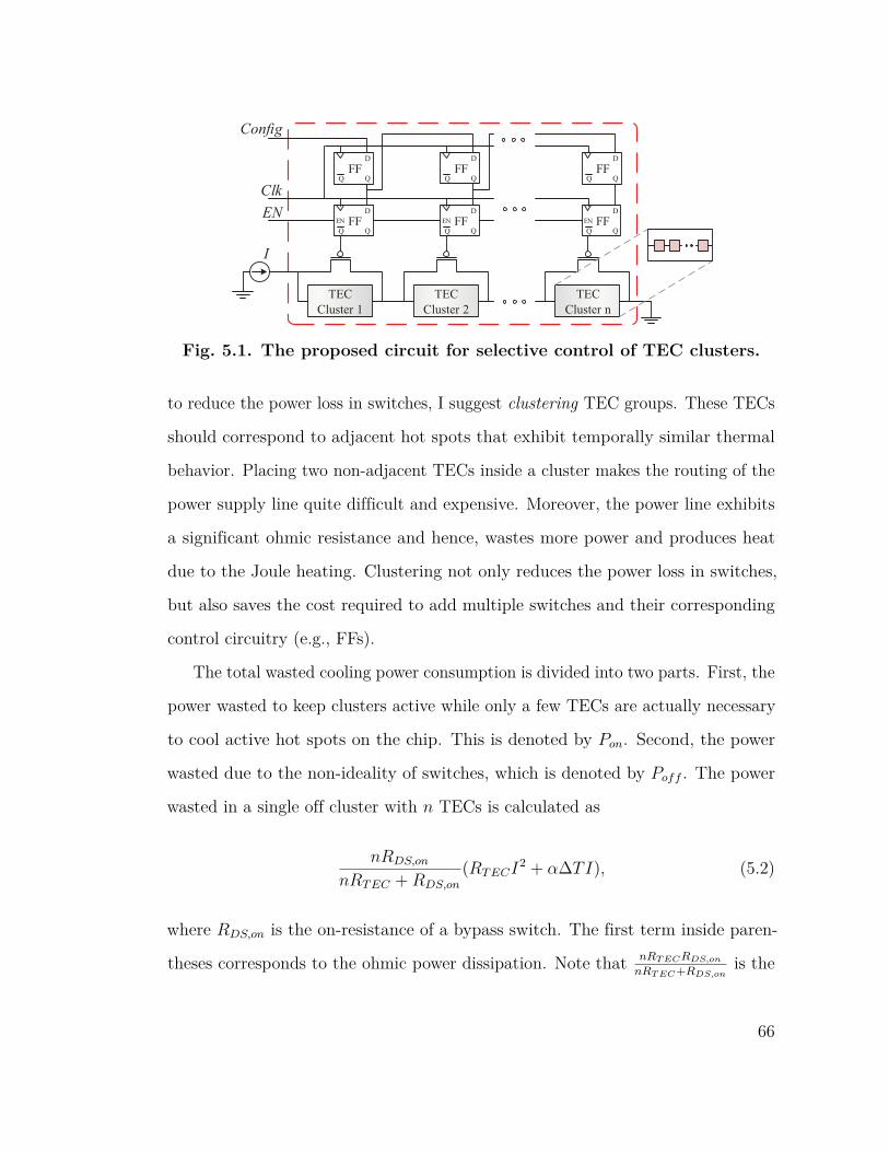
Fig. 5.1. The proposed circuit for selective control of TEC clusters.
to reduce the power loss in switches, I suggest clustering TEC groups. These TECs
should correspond to adjacent hot spots that exhibit temporally similar thermal
behavior. Placing two non-adjacent TECs inside a cluster makes the routing of the
power supply line quite difficult and expensive. Moreover, the power line exhibits
a significant ohmic resistance and hence, wastes more power and produces heat
due to the Joule heating. Clustering not only reduces the power loss in switches,
but also saves the cost required to add multiple switches and their corresponding
control circuitry (e.g., FFs).
The total wasted cooling power consumption is divided into two parts. First, the
power wasted to keep clusters active while only a few TECs are actually necessary
to cool active hot spots on the chip. This is denoted by 𝑃𝑜𝑛. Second, the power
wasted due to the non-ideality of switches, which is denoted by 𝑃𝑜𝑓𝑓 . The power
wasted in a single off cluster with 𝑛 TECs is calculated as
𝑛𝑅𝐷𝑆,𝑜𝑛
𝑛𝑅𝑇 𝐸𝐶 + 𝑅𝐷𝑆,𝑜𝑛
(𝑅𝑇 𝐸𝐶𝐼2 + 𝛼Δ𝑇𝐼), (5.2)
where 𝑅𝐷𝑆,𝑜𝑛 is the on-resistance of a bypass switch. The first term inside paren-
theses corresponds to the ohmic power dissipation. Note that 𝑛𝑅𝑇 𝐸𝐶𝑅𝐷𝑆,𝑜𝑛
𝑛𝑅𝑇 𝐸𝐶+𝑅𝐷𝑆,𝑜𝑛is the
66
equivalent resistance for a cluster of TECs paralleled with a bypass switch. The
second term is due to the TEC power dissipation only (cf. Eq. (2.3)). 𝑃𝑜𝑓𝑓 can
be calculated as a summation over Eq. (5.2) written for every off cluster. Clearly,
𝑃𝑜𝑓𝑓 is minimized when 𝑛 is maximized, i.e., all TECs are grouped into a single
cluster. On the other hand, increasing 𝑛 reduces the controllability of TECs, and
consequently, increases 𝑃𝑜𝑛. Hence, there should be an optimum clustering solution
for which the wasted power consumption for driving TECs (i.e., 𝑃𝑜𝑛 + 𝑃𝑜𝑓𝑓) is
minimized. Next section will present an optimization problem that finds such
clustering.
5.3 TEC Clustering
5.3.1 Problem Formulation
I assume that an exhaustive set of applications are executed on the target chip
and their corresponding temperature maps are derived. This step, which is referred
as the benchmarking step, is a common practice for determining best locations to
place temperature sensors on the die (e.g., see [51] and [54]). Based on the derived
temperature map(s) for each application, a set of intervals for hot spots can be
determined. Each interval depicts a hot spot which is present during the execution
of an application (i.e., its temperature is higher than a certain threshold). Given
this thermal information, one may find a near-optimum minimum set of TECs
required for cooling down these hot spots as explained in [29].
Next, these TECs are grouped such that members of each group always behave
similarly, i.e., they target the same hot spot. Due to the small size of TECs, I
assume that each hot spot can be cooled down by one or several TECs. Finally,
TEC groups are clustered and each cluster is controlled by a bypass switch in order
67
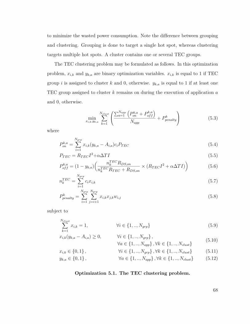
to minimize the wasted power consumption. Note the difference between grouping
and clustering. Grouping is done to target a single hot spot, whereas clustering
targets multiple hot spots. A cluster contains one or several TEC groups.
The TEC clustering problem may be formulated as follows. In this optimization
problem, 𝑥𝑖,𝑘 and 𝑦𝑘,𝑎 are binary optimization variables. 𝑥𝑖,𝑘 is equal to 1 if TEC
group 𝑖 is assigned to cluster 𝑘 and 0, otherwise. 𝑦𝑘,𝑎 is equal to 1 if at least one
TEC group assigned to cluster 𝑘 remains on during the execution of application 𝑎
and 0, otherwise.
min𝑥𝑖,𝑘,𝑦𝑘,𝑎
𝑁𝑐𝑙𝑢𝑠𝑡∑︁𝑘=1
⎛⎝∑︀𝑁𝑎𝑝𝑝
𝑎=1
(︁𝑃 𝑘,𝑎
𝑜𝑛 + 𝑃 𝑘,𝑎𝑜𝑓𝑓
)︁𝑁𝑎𝑝𝑝
+ 𝑃 𝑘𝑝𝑒𝑛𝑎𝑙𝑡𝑦
⎞⎠ (5.3)
where
𝑃 𝑘,𝑎𝑜𝑛 =
𝑁𝑔𝑟𝑝∑︁𝑖=1
𝑥𝑖,𝑘(𝑦𝑘,𝑎 − 𝐴𝑖,𝑎)𝑐𝑖𝑃𝑇 𝐸𝐶 (5.4)
𝑃𝑇 𝐸𝐶 = 𝑅𝑇 𝐸𝐶𝐼2+𝛼Δ𝑇𝐼 (5.5)
𝑃 𝑘,𝑎𝑜𝑓𝑓 = (1− 𝑦𝑘,𝑎)
(︂𝑛𝑇 𝐸𝐶
𝑘 𝑅𝐷𝑆,𝑜𝑛
𝑛𝑇 𝐸𝐶𝑘 𝑅𝑇 𝐸𝐶 + 𝑅𝐷𝑆,𝑜𝑛
× (𝑅𝑇 𝐸𝐶𝐼2 + 𝛼Δ𝑇𝐼))︂
(5.6)
𝑛𝑇 𝐸𝐶𝑘 =
𝑁𝑔𝑟𝑝∑︁𝑖=1
𝑐𝑖𝑥𝑖,𝑘 (5.7)
𝑃 𝑘𝑝𝑒𝑛𝑎𝑙𝑡𝑦 =
𝑁𝑔𝑟𝑝∑︁𝑖=1
𝑁𝑔𝑟𝑝∑︁𝑗=𝑖+1
𝑥𝑖,𝑘𝑥𝑗,𝑘𝑤𝑖,𝑗 (5.8)
subject to
𝑁𝑐𝑙𝑢𝑠𝑡∑︁𝑘=1
𝑥𝑖,𝑘 = 1, ∀𝑖 ∈ {1, .., 𝑁𝑔𝑟𝑝} (5.9)
𝑥𝑖,𝑘(𝑦𝑘,𝑎 − 𝐴𝑖,𝑎) ≥ 0, ∀𝑖 ∈ {1, .., 𝑁𝑔𝑟𝑝} ,
∀𝑎 ∈ {1, .., 𝑁𝑎𝑝𝑝} ,∀𝑘 ∈ {1, .., 𝑁𝑐𝑙𝑢𝑠𝑡}(5.10)
𝑥𝑖,𝑘 ∈ {0, 1} , ∀𝑖 ∈ {1, .., 𝑁𝑔𝑟𝑝} ,∀𝑘 ∈ {1, .., 𝑁𝑐𝑙𝑢𝑠𝑡} (5.11)𝑦𝑘,𝑎 ∈ {0, 1} , ∀𝑎 ∈ {1, .., 𝑁𝑎𝑝𝑝} , ∀𝑘 ∈ {1, .., 𝑁𝑐𝑙𝑢𝑠𝑡} (5.12)
Optimization 5.1. The TEC clustering problem.
68
The definition of parameters in this problem follows:
∙ 𝑃 𝑘,𝑎𝑜𝑛 and 𝑃 𝑘,𝑎
𝑜𝑓𝑓 are wasted power consumption values during the execution of
application 𝑎 when cluster 𝑘 is on (i.e., its corresponding switch is open) and
off (i.e., its corresponding switch is closed), respectively.
∙ 𝑃 𝑘𝑝𝑒𝑛𝑎𝑙𝑡𝑦 is the penalty value imposed due to the distance of TEC groups
assigned to cluster 𝑘.
∙ 𝑁𝑐𝑙𝑢𝑠𝑡 is the maximum number of clusters that are allowed to be formed. This
value is determined by the cooling package budget.
∙ 𝑁𝑔𝑟𝑝 is the total number of TEC groups.
∙ 𝑁𝑎𝑝𝑝 is the number of representative applications executed on the VLSI chip
during the benchmarking step.
∙ 𝑐𝑖 is the number of TECs inside TEC group 𝑖.
∙ 𝐴𝑖,𝑎 determines if TEC group 𝑖 is active during the execution of application
𝑎 or not. The value of this parameter may be found from the set of intervals
derived earlier.
∙ 𝑤𝑖,𝑗 is a monotonically increasing function of the distance of TEC groups 𝑖
and 𝑗 which are placed in the same cluster.
∙ 𝑅𝐷𝑆,𝑜𝑛, 𝛼, Δ𝑇 , 𝑅𝑇 𝐸𝐶 , and 𝐼 are defined as before.
The objective function (shown in Eq. (5.3)) tries to minimize the summation
of the average total power waste among clusters when they are unnecessarily on
(𝑃 𝑘,𝑎𝑜𝑛 ), the average total power waste due to the non-ideality of bypass switches for
each cluster (𝑃 𝑘,𝑎𝑜𝑓𝑓 ), and a penalty value (𝑃 𝑘
𝑝𝑒𝑛𝑎𝑙𝑡𝑦) imposed due to the non-locality
of TEC groups inside a cluster.
69
Eq. (5.4) defines 𝑃 𝑘,𝑎𝑜𝑛 . Basically, a TEC group wastes power when it should be
off (i.e., 𝐴𝑖,𝑎 = 0), but its corresponding cluster 𝑘 is on during the execution of
application 𝑎 (i.e., 𝑦𝑘,𝑎 = 1). 𝑃𝑇 𝐸𝐶 is defined in Eq. (5.5) similar to Eq. (2.3).
Next, Eq. (5.6) defines 𝑃 𝑘,𝑎𝑜𝑓𝑓 . Note that 𝑃 𝑘,𝑎
𝑜𝑓𝑓 has a non-zero value only if cluster
𝑘 is off during the execution of application 𝑎 (𝑦𝑘,𝑎 = 0). This equation is written
similar to Eq. (5.2); however, instead of 𝑛, 𝑛𝑇 𝐸𝐶𝑘 is used, which is defined as the
total number of TECs in cluster 𝑘 (cf. Eq. (5.7)).
Eq. (5.8) defines 𝑃 𝑘𝑝𝑒𝑛𝑎𝑙𝑡𝑦. This value is the summation of penalty values among
every pair of TEC groups assigned to cluster 𝑘. 𝑤𝑖,𝑗 is a function of the distance
between TEC groups 𝑖 and 𝑗. In this chapter, I define it as follows. If TEC groups 𝑖
and 𝑗 are not adjacent (i.e., farther apart than the distance 𝑟 from each other), 𝑤𝑖,𝑗
is set to a large positive number; otherwise, it is set to zero. With this definition, I
make sure that TEC groups with any distance higher than 𝑟 from each other are
not assigned to same the cluster, unless 𝑁𝑐𝑙𝑢𝑠𝑡 is set to a very small number.
Constraint (5.9) ensures that all of TEC groups are assigned to a cluster.
Constraint (5.10) assures that cluster 𝑘 is active during the execution of application
𝑎, if TEC group 𝑖 is active during the same period and it is assigned to cluster 𝑘
(i.e., 𝑥𝑖,𝑘 = 1). Finally, constraints (5.11) and (5.12) ensure that 𝑥𝑖,𝑘 and 𝑦𝑘,𝑎 are
binary variables.
5.3.2 Proposed Solution
The problem formulation presented above is not a standard 0–1 integer-quadratic
program (0–1 IQP). The only non-quadratic term is the definition of 𝑃 𝑘𝑜𝑓𝑓 in Eq. (5.6).
70
Due to the nature of the problem, the total number of TECs in a cluster is large
and hence 𝑛𝑇 𝐸𝐶𝑘 𝑅𝑇 𝐸𝐶 ≫ 𝑅𝐷𝑆,𝑜𝑛. Thus,
𝑃 𝑘,𝑎𝑜𝑓𝑓 ≈ (1− 𝑦𝑘,𝑎)
(︂𝑅𝐷𝑆,𝑜𝑛𝐼2 + 𝑅𝐷𝑆,𝑜𝑛
𝑅𝑇 𝐸𝐶
𝛼Δ𝑇𝐼)︂
. (5.13)
Using the aforementioned simplification, the problem formulation becomes a
standard 0–1 IQP. Unfortunately, the number of optimization variables are too
high for problems of interesting sizes. More precisely, this problem has a total
of 𝑁𝑐𝑙𝑢𝑠𝑡(𝑁𝑎𝑝𝑝 + 𝑁𝑔𝑟𝑝) binary variables. Clearly, it cannot be optimally solved for
reasonable values of 𝑁𝑐𝑙𝑢𝑠𝑡, 𝑁𝑎𝑝𝑝, and 𝑁𝑔𝑟𝑝.
Hence, I propose a greedy heuristic to solve the clustering problem. The
pseudocode of this heuristic is listed in Algorithm 5.1. As it will be shown in
the experimental results section, this heuristic saves substantial amount of wasted
power by generating high-quality clustering solutions. Note that the heuristic is
executed during the design of the cooling system and hence, have no impact on
the performance and power consumption of the system. Subsequently, during the
runtime of the system, if at least a single hot spot corresponding to a cluster is
present, the bypass switch of that cluster should be off (does not bypass). Otherwise,
the switch should be on (bypasses).
First, (lines 1–8), 𝑧𝑖 is calculated for each TEC group which represents how
many times any TEC in group 𝑖 is active during the execution of 𝑁𝑎𝑝𝑝 applications.
In this heuristic, TEC groups which have higher 𝑧𝑖 are processed first, since they
are more critical. This is done through sorting G (i.e., the list of TEC groups)
based on calculated 𝑧𝑖 values (line 9).
The rest of the algorithm is straightforward. It picks a TEC group from G and
tries every cluster that is already formed in S. It chooses the cluster which has the
71
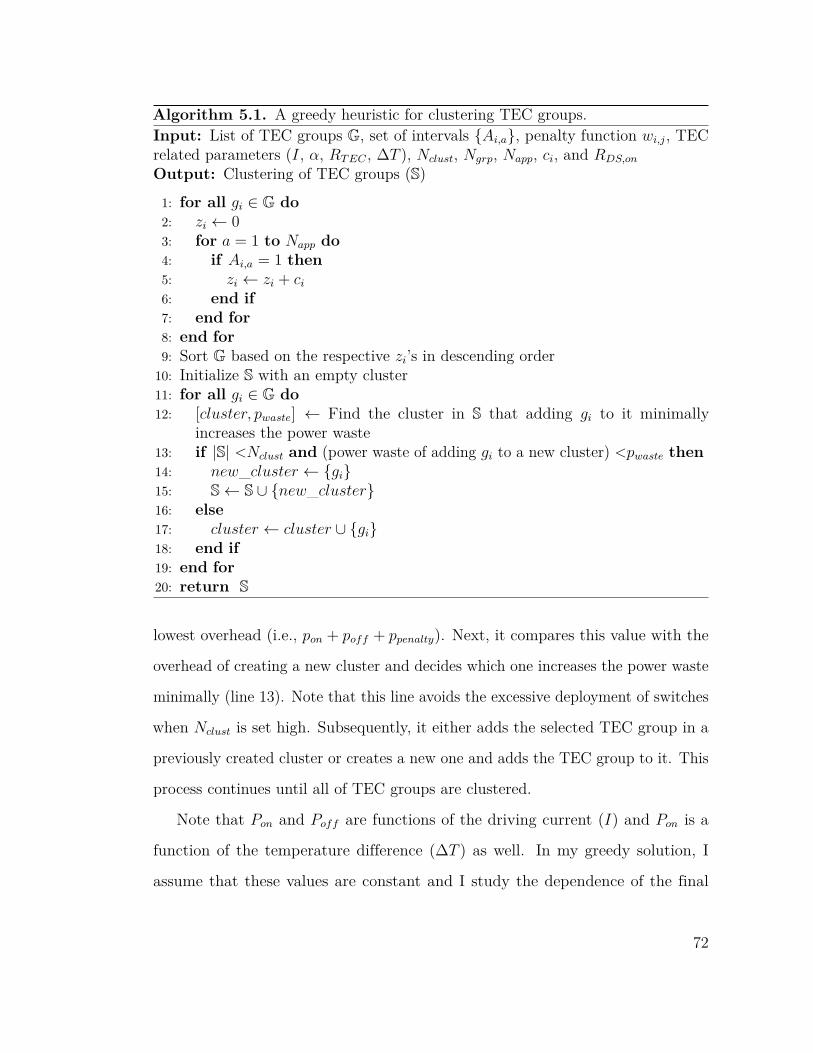
Algorithm 5.1. A greedy heuristic for clustering TEC groups.Input: List of TEC groups G, set of intervals {𝐴𝑖,𝑎}, penalty function 𝑤𝑖,𝑗, TECrelated parameters (𝐼, 𝛼, 𝑅𝑇 𝐸𝐶 , Δ𝑇 ), 𝑁𝑐𝑙𝑢𝑠𝑡, 𝑁𝑔𝑟𝑝, 𝑁𝑎𝑝𝑝, 𝑐𝑖, and 𝑅𝐷𝑆,𝑜𝑛
Output: Clustering of TEC groups (S)
1: for all 𝑔𝑖 ∈ G do2: 𝑧𝑖 ← 03: for 𝑎 = 1 to 𝑁𝑎𝑝𝑝 do4: if 𝐴𝑖,𝑎 = 1 then5: 𝑧𝑖 ← 𝑧𝑖 + 𝑐𝑖
6: end if7: end for8: end for9: Sort G based on the respective 𝑧𝑖’s in descending order
10: Initialize S with an empty cluster11: for all 𝑔𝑖 ∈ G do12: [𝑐𝑙𝑢𝑠𝑡𝑒𝑟, 𝑝𝑤𝑎𝑠𝑡𝑒] ← Find the cluster in S that adding 𝑔𝑖 to it minimally
increases the power waste13: if |S| <𝑁𝑐𝑙𝑢𝑠𝑡 and (power waste of adding 𝑔𝑖 to a new cluster) <𝑝𝑤𝑎𝑠𝑡𝑒 then14: 𝑛𝑒𝑤_𝑐𝑙𝑢𝑠𝑡𝑒𝑟 ← {𝑔𝑖}15: S← S ∪ {𝑛𝑒𝑤_𝑐𝑙𝑢𝑠𝑡𝑒𝑟}16: else17: 𝑐𝑙𝑢𝑠𝑡𝑒𝑟 ← 𝑐𝑙𝑢𝑠𝑡𝑒𝑟 ∪ {𝑔𝑖}18: end if19: end for20: return S
lowest overhead (i.e., 𝑝𝑜𝑛 + 𝑝𝑜𝑓𝑓 + 𝑝𝑝𝑒𝑛𝑎𝑙𝑡𝑦). Next, it compares this value with the
overhead of creating a new cluster and decides which one increases the power waste
minimally (line 13). Note that this line avoids the excessive deployment of switches
when 𝑁𝑐𝑙𝑢𝑠𝑡 is set high. Subsequently, it either adds the selected TEC group in a
previously created cluster or creates a new one and adds the TEC group to it. This
process continues until all of TEC groups are clustered.
Note that 𝑃𝑜𝑛 and 𝑃𝑜𝑓𝑓 are functions of the driving current (𝐼) and 𝑃𝑜𝑛 is a
function of the temperature difference (Δ𝑇 ) as well. In my greedy solution, I
assume that these values are constant and I study the dependence of the final
72
solution on them through sensitivity analysis in the next section.
5.4 Experimental Results
5.4.1 Simulation Setup
It is expected that a multi-core processor exhibit more non-uniformly distributed
hot spots compared to a single-core processor. Hence, I selected a quad-core Intel
Xeon X5550 running at 3.06GHz [55] as the target chip. SniperSim 5.3 [56] is used
as the performance simulator. It utilizes McPat 1.0 [43] to generate area and power
information for a given set of a processor and a benchmark. Using the area and
power information that McPat provides, I employ HotFloorplan [57] in order to
generate a temperature-aware floorplan for the Xeon X5550 processor. The aspect
ratio of this floorplan is 19.1 mm×10.2 mm. PARSEC benchmark suite [58], which
consists of multi-threaded applications, is chosen to be executed on the processor.
For thermal simulations, Teculator is employed (see Chapter 3 and Chapter 4).
Teculator and some other prior art such as [26] assume that leakage power depends
only on the temperature and area. I improve this simple model by utilizing McPat
leakage models for various functional units. This captures the dependence of the
leakage current to the circuit implementation of each functional unit. For instance,
the leakage current of ALU differs from that of the instruction cache (ICache).
A cooling package similar to Fig. 2.3 is adopted for the simulations. Main
component characteristics are taken from Chapter 3. A fan with the rotational
speed of 1000 RPM is also used for improving the cooling efficiency of TECs. TEC
properties are taken form [13], which is the state-of-the-art in the thermoelectric
cooling technology.
73
Moreover, I select Texas Instrument’s TPS22920L [52] as the bypass switch,
which has 𝑅𝐷𝑆,𝑜𝑛=5 mΩ and a very large 𝑅𝐷𝑆,𝑜𝑓𝑓 . I also set Δ𝑇=10 K, and
r=4.775 mm (i.e., a quarter of the floorplan width) unless otherwise is mentioned.
Furthermore, 𝐼 is set to 3 A, which is close to the optimal TEC power-efficiency
point in my setup.
The proposed heuristic is implemented in Java and executed on a machine
with Intel Core-i7 3770 running at 3.4 GHz with 8 GB RAM. The runtime of the
program is less than one second, which is spent during the design time.
5.4.2 Simulation Results
First, the thermal behavior of the Xeon processor is simulated by running
PARSEC benchmarks. These simulations provide a steady-state temperature map
for each benchmark. As it is expected, some benchmarks exhibit quite different
temperature maps and some quite similar maps compared to the others. Using
these temperature maps, a list of hot spots for each benchmark is made. I consider
a spot as hot if its temperature exceeds 85 ∘C. Next, I find the minimum number of
TECs that are sufficient to cool down these spots. This provides a baseline which
only considers the spatial distribution of hot spots.
Using these data, a set of intervals is obtained as shown in Fig. 5.2. Each TEC
group is named using the processing core and the functional unit it targets. The
number of TECs inside each group is determined in parenthesis. A green block
shows that a TEC group should be active during a benchmark in order to maintain
the temperature of the hottest spot on the die below 85 ∘C. For instance, TECs in
group Core1-Mem are required to be active only during the execution of benchmark
raytrace.
74
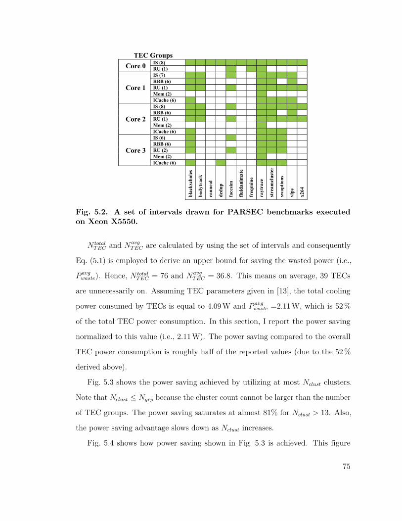
Fig. 5.2. A set of intervals drawn for PARSEC benchmarks executedon Xeon X5550.
𝑁 𝑡𝑜𝑡𝑎𝑙𝑇 𝐸𝐶 and 𝑁𝑎𝑣𝑔
𝑇 𝐸𝐶 are calculated by using the set of intervals and consequently
Eq. (5.1) is employed to derive an upper bound for saving the wasted power (i.e.,
𝑃 𝑎𝑣𝑔𝑤𝑎𝑠𝑡𝑒). Hence, 𝑁 𝑡𝑜𝑡𝑎𝑙
𝑇 𝐸𝐶 = 76 and 𝑁𝑎𝑣𝑔𝑇 𝐸𝐶 = 36.8. This means on average, 39 TECs
are unnecessarily on. Assuming TEC parameters given in [13], the total cooling
power consumed by TECs is equal to 4.09 W and 𝑃 𝑎𝑣𝑔𝑤𝑎𝑠𝑡𝑒 =2.11 W, which is 52 %
of the total TEC power consumption. In this section, I report the power saving
normalized to this value (i.e., 2.11 W). The power saving compared to the overall
TEC power consumption is roughly half of the reported values (due to the 52 %
derived above).
Fig. 5.3 shows the power saving achieved by utilizing at most 𝑁𝑐𝑙𝑢𝑠𝑡 clusters.
Note that 𝑁𝑐𝑙𝑢𝑠𝑡 ≤ 𝑁𝑔𝑟𝑝 because the cluster count cannot be larger than the number
of TEC groups. The power saving saturates at almost 81% for 𝑁𝑐𝑙𝑢𝑠𝑡 > 13. Also,
the power saving advantage slows down as 𝑁𝑐𝑙𝑢𝑠𝑡 increases.
Fig. 5.4 shows how power saving shown in Fig. 5.3 is achieved. This figure
75
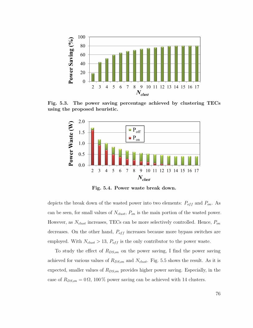
0
20
40
60
80
100
2 3 4 5 6 7 8 9 10 11 12 13 14 15 16 17
Pow
er S
avin
g (%
)
Nclust
Fig. 5.3. The power saving percentage achieved by clustering TECsusing the proposed heuristic.
0.0
0.5
1.0
1.5
2.0
2 3 4 5 6 7 8 9 10 11 12 13 14 15 16 17
Pow
er W
aste
(W)
Nclust
P_off
P_on
PoffPon
Fig. 5.4. Power waste break down.
depicts the break down of the wasted power into two elements: 𝑃𝑜𝑓𝑓 and 𝑃𝑜𝑛. As
can be seen, for small values of 𝑁𝑐𝑙𝑢𝑠𝑡, 𝑃𝑜𝑛 is the main portion of the wasted power.
However, as 𝑁𝑐𝑙𝑢𝑠𝑡 increases, TECs can be more selectively controlled. Hence, 𝑃𝑜𝑛
decreases. On the other hand, 𝑃𝑜𝑓𝑓 increases because more bypass switches are
employed. With 𝑁𝑐𝑙𝑢𝑠𝑡 > 13, 𝑃𝑜𝑓𝑓 is the only contributor to the power waste.
To study the effect of 𝑅𝐷𝑆,𝑜𝑛 on the power saving, I find the power saving
achieved for various values of 𝑅𝐷𝑆,𝑜𝑛 and 𝑁𝑐𝑙𝑢𝑠𝑡. Fig. 5.5 shows the result. As it is
expected, smaller values of 𝑅𝐷𝑆,𝑜𝑛 provides higher power saving. Especially, in the
case of 𝑅𝐷𝑆,𝑜𝑛 = 0 Ω, 100 % power saving can be achieved with 14 clusters.
76
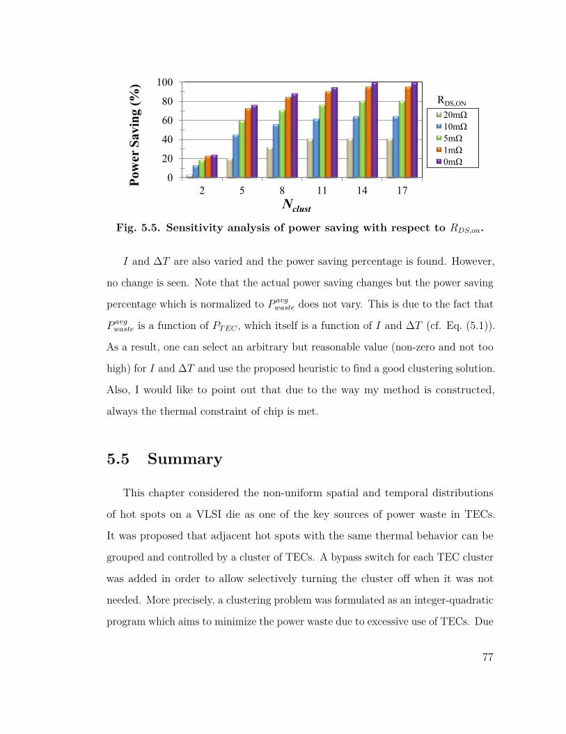
0
20
40
60
80
100
2 5 8 11 14 17
Pow
er S
avin
g (%
)
Nclust
20mΩ 10mΩ 5mΩ 1mΩ0mΩ
RDS,ON
Fig. 5.5. Sensitivity analysis of power saving with respect to 𝑅𝐷𝑆,𝑜𝑛.
𝐼 and Δ𝑇 are also varied and the power saving percentage is found. However,
no change is seen. Note that the actual power saving changes but the power saving
percentage which is normalized to 𝑃 𝑎𝑣𝑔𝑤𝑎𝑠𝑡𝑒 does not vary. This is due to the fact that
𝑃 𝑎𝑣𝑔𝑤𝑎𝑠𝑡𝑒 is a function of 𝑃𝑇 𝐸𝐶 , which itself is a function of 𝐼 and Δ𝑇 (cf. Eq. (5.1)).
As a result, one can select an arbitrary but reasonable value (non-zero and not too
high) for 𝐼 and Δ𝑇 and use the proposed heuristic to find a good clustering solution.
Also, I would like to point out that due to the way my method is constructed,
always the thermal constraint of chip is met.
5.5 Summary
This chapter considered the non-uniform spatial and temporal distributions
of hot spots on a VLSI die as one of the key sources of power waste in TECs.
It was proposed that adjacent hot spots with the same thermal behavior can be
grouped and controlled by a cluster of TECs. A bypass switch for each TEC cluster
was added in order to allow selectively turning the cluster off when it was not
needed. More precisely, a clustering problem was formulated as an integer-quadratic
program which aims to minimize the power waste due to excessive use of TECs. Due
77
to the large number of variables in problems of interesting sizes, a greedy heuristic
method for solving the problem was introduced. It was shown that the proposed
heuristic can reduce the wasted power on average by 81% and also decrease the
total TEC power consumption on average by 42%.
78
6Thermoelectric Generators Modeling
6.1 Overview
Energy harvesting has gained significant attention due to the ever increasing
demand for energy. Harvested energies are usually renewable energies (such as
solar, wind, etc.) or otherwise wasted energies (like heat) [34]. Abundance and
availability at no cost make harvesting of the electrical energy out of those sources
quite attractive. One of such energy sources is heat, which can be converted into
electricity by means of thermoelectric generators (TEGs).
Despite the appealing characteristics of TEGs listed in Chapter 2, they suffer
from low conversion efficiency, which is imposed by two main factors. First, the
Carnot cycle efficiency, which sets a theoretical upper bound on the conversion
efficiency of thermal energy to work, can be quite low. Specifically, this efficiency
is defined as 𝜂𝐶𝑎𝑟𝑛𝑜𝑡 = Δ𝑇/𝑇ℎ, where 𝑇ℎ is the temperature of the hot side and
Δ𝑇 is the temperature difference between hot and cold sides. Clearly, when Δ𝑇
is small, the conversion efficiency is quite low. For instance, 30 K temperature
difference in the room temperature (300 K) can provide up to 10% efficiency. The
79
second limiting factor is the efficiency of the thermoelectric effect. The overall
TEG efficiency can be formulated as [22]
𝜂𝑇 𝐸𝐺
= Δ𝑇
𝑇ℎ
.
√︁1 + 𝑍𝑇𝑎𝑣𝑔 − 1√︁
1 + 𝑍𝑇𝑎𝑣𝑔 + 𝑇𝑐/𝑇ℎ
, (6.1)
where 𝑍 is the TEG figure of merit and 𝑇𝑎𝑣𝑔 = (𝑇ℎ + 𝑇𝑐)/2. State-of-the-art TEGs
have 𝑍𝑇𝑎𝑣𝑔 value of 2.1 for 𝑇𝑎𝑣𝑔 = 300𝐾 (27∘C) [13]. For the same temperature
difference used above, the efficiency of this TEG is equal to only 2.8%, which is 72%
lower than that of an ideal Carnot cycle. Evidently, the efficiency of TEGs is quite
low. Low efficiency limits the usage of TEGs to low-power applications. Note that
usually the overall energy of the source is rather low, e.g., the heat generated from
the human body. This factor also limits the amount of harvested energy. Devices
with power consumption of 100 mW or less are ideal targets to be powered by
thermoelectric generators, whereas devices with higher power consumption require
larger temperature gradient in order to be powered by TEGs.
The process of converting the temperature difference to usable electrical energy
involves two steps. First, TEGs convert the temperature difference into an electrical
voltage which is usually not suitable for the load and needs to be regulated. Next,
this voltage is converted by an interface circuit to a regulated voltage required by
the load or the energy storage element. This process is shown in Fig. 6.1. Note
that in order to extract the maximum power from the generator and transfer it
to the load, the interface circuit input resistance (𝑅𝑖𝑛𝑖𝑓𝑎𝑐𝑒) must be matched to the
TEG internal resistance (𝑅𝑖𝑛𝑇 𝐸𝐺,𝑁). This step is necessary to avoid losses in an
already-low harvested energy.
In the prior art (such as [21], [34], [35], and [36]), 𝑅𝑖𝑛𝑇 𝐸𝐺 was set to be equal to
the electrical resistance of the thermoelectric module (𝑅𝑇 𝐸𝐺,𝑁). In this chapter, I
80
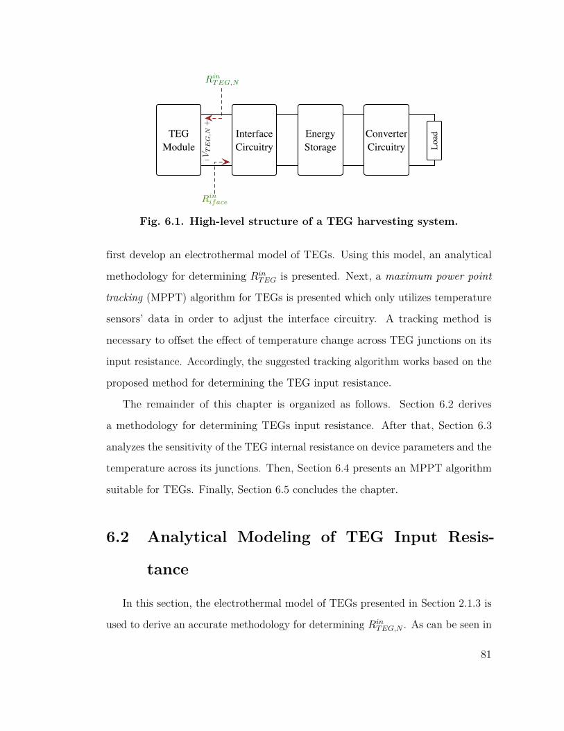
Riniface
VT
EG
,N
+
�
RinTEG,N
Interface Circuitry
Energy Storage
Converter Circuitry Lo
adTEGModule
Fig. 6.1. High-level structure of a TEG harvesting system.
first develop an electrothermal model of TEGs. Using this model, an analytical
methodology for determining 𝑅𝑖𝑛𝑇 𝐸𝐺 is presented. Next, a maximum power point
tracking (MPPT) algorithm for TEGs is presented which only utilizes temperature
sensors’ data in order to adjust the interface circuitry. A tracking method is
necessary to offset the effect of temperature change across TEG junctions on its
input resistance. Accordingly, the suggested tracking algorithm works based on the
proposed method for determining the TEG input resistance.
The remainder of this chapter is organized as follows. Section 6.2 derives
a methodology for determining TEGs input resistance. After that, Section 6.3
analyzes the sensitivity of the TEG internal resistance on device parameters and the
temperature across its junctions. Then, Section 6.4 presents an MPPT algorithm
suitable for TEGs. Finally, Section 6.5 concludes the chapter.
6.2 Analytical Modeling of TEG Input Resis-
tance
In this section, the electrothermal model of TEGs presented in Section 2.1.3 is
used to derive an accurate methodology for determining 𝑅𝑖𝑛𝑇 𝐸𝐺,𝑁 . As can be seen in
81
Fig. 2.5, a TEG is subjected to a temperature differential through its metal contacts.
The thermal and electrical contact resistances of TEGs are not negligible [13]. The
contact thermal resistance (Θ𝑐𝑜𝑛𝑡,𝑁) causes the temperature at surfaces of a TEG
module (i.e., 𝑇 ′𝑐 and 𝑇 ′
ℎ) differ from the temperature on the N- and P-type pellets
(i.e., 𝑇𝑐 and 𝑇ℎ). Assuming that 𝑇 ′𝑐 and 𝑇 ′
ℎ are set externally, values of 𝑇𝑐 and
𝑇ℎ depend on parameters of the TEG shown in the thermal part. Consequently,
this affects the internal resistance of the TEG. In order to determine the TEG
internal resistance, the usual procedure consists in deriving a Thévenin equivalent
circuit. However, the electrothermal model of TEGs is a non-linear circuit. The
non-linearity is produced by the thermal part, where a current-controlled voltage
source generates a voltage that is a quadratic function of the current 𝐼 in the
electrical circuit. Hence, the Thévenin’s theorem cannot be applied to this circuit.
Therefore, the load resistance seen by the TEG module that maximizes the
power consumed in the load is directly found. Note that the maximization of
conversion efficiency of TEGs is a different objective. Efficiency is maximized for
large values of the load resistance [59]. However, since the TEG source energy (i.e.,
heat) is available for free, the conversion efficiency is not of interest and hence the
objective is to maximize the power transferred to the load.
Suppose the interface circuit has the input resistance 𝑅𝑖𝑛𝑖𝑓𝑎𝑐𝑒 seen from output
terminals of the TEG module. 𝑉𝑇 𝐸𝐺,𝑁 and 𝐼 denote the voltage and the current,
respectively, across 𝑅𝑖𝑛𝑖𝑓𝑎𝑐𝑒. Clearly, the following optimization problem should be
solved to find the optimal 𝑅𝑖𝑛𝑖𝑓𝑎𝑐𝑒 (called 𝑅𝑖𝑛*
𝑖𝑓𝑎𝑐𝑒).
𝑅𝑖𝑛*𝑖𝑓𝑎𝑐𝑒 = argmax
𝑅𝑖𝑛𝑖𝑓𝑎𝑐𝑒
{𝑉 2𝑇 𝐸𝐺,𝑁/𝑅𝑖𝑛
𝑖𝑓𝑎𝑐𝑒} (6.2)
82
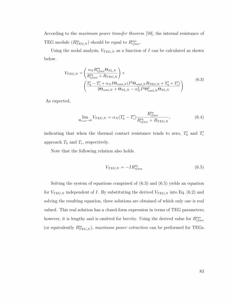
According to the maximum power transfer theorem [59], the internal resistance of
TEG module (𝑅𝑖𝑛𝑇 𝐸𝐺,𝑁) should be equal to 𝑅𝑖𝑛*
𝑖𝑓𝑎𝑐𝑒.
Using the nodal analysis, 𝑉𝑇 𝐸𝐺,𝑁 as a function of 𝐼 can be calculated as shown
below.
𝑉𝑇 𝐸𝐺,𝑁 =(︃
𝛼𝑁 𝑅𝑖𝑛𝑖𝑓𝑎𝑐𝑒Θ𝑆𝐿,𝑁
𝑅𝑖𝑛𝑖𝑓𝑎𝑐𝑒 + 𝑅𝑇 𝐸𝐺,𝑁
)︃×(︃
𝑇 ′ℎ − 𝑇 ′
𝑐 + 𝛼𝑁 𝐼Θ𝑐𝑜𝑛𝑡,𝑁 (𝐼2Θ𝑐𝑜𝑛𝑡,𝑁 𝑅TEG,N + 𝑇 ′ℎ + 𝑇 ′
𝑐)2Θ𝑐𝑜𝑛𝑡,𝑁 + Θ𝑆𝐿,𝑁 − 𝛼2
𝑁 𝐼2Θ2𝑐𝑜𝑛𝑡,𝑁 Θ𝑆𝐿,𝑁
)︃ (6.3)
As expected,
limΘ𝑐𝑜𝑛𝑡→0
𝑉𝑇 𝐸𝐺,𝑁 = 𝛼𝑁(𝑇 ′ℎ − 𝑇 ′
𝑐)𝑅𝑖𝑛
𝑖𝑓𝑎𝑐𝑒
𝑅𝑖𝑛𝑖𝑓𝑎𝑐𝑒 + 𝑅𝑇 𝐸𝐺,𝑁
, (6.4)
indicating that when the thermal contact resistance tends to zero, 𝑇 ′ℎ and 𝑇 ′
𝑐
approach 𝑇ℎ and 𝑇𝑐, respectively.
Note that the following relation also holds.
𝑉𝑇 𝐸𝐺,𝑁 = −𝐼𝑅𝑖𝑛𝑖𝑓𝑎𝑐𝑒 (6.5)
Solving the system of equations comprised of (6.3) and (6.5) yields an equation
for 𝑉𝑇 𝐸𝐺,𝑁 independent of 𝐼. By substituting the derived 𝑉𝑇 𝐸𝐺,𝑁 into Eq. (6.2) and
solving the resulting equation, three solutions are obtained of which only one is real
valued. This real solution has a closed-form expression in terms of TEG parameters;
however, it is lengthy and is omitted for brevity. Using the derived value for 𝑅𝑖𝑛*𝑖𝑓𝑎𝑐𝑒
(or equivalently 𝑅𝑖𝑛𝑇 𝐸𝐺,𝑁), maximum power extraction can be performed for TEGs.
83
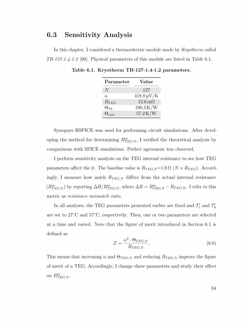
6.3 Sensitivity Analysis
In this chapter, I considered a thermoelectric module made by Kryotherm called
TB-127-1.4-1.2 [60]. Physical parameters of this module are listed in Table 6.1.
Table 6.1. Kryotherm TB-127-1.4-1.2 parameters.
Parameter Value𝑁 127𝛼 418.8 µV/K𝑅𝑇 𝐸𝐺 12.6 mΩΘ𝑆𝐿 190.3 K/WΘ𝑐𝑜𝑛𝑡 57.2 K/W
Synopsys HSPICE was used for performing circuit simulations. After devel-
oping the method for determining 𝑅𝑖𝑛𝑇 𝐸𝐺,𝑁 , I verified the theoretical analysis by
comparisons with SPICE simulations. Perfect agreement was observed.
I perform sensitivity analysis on the TEG internal resistance to see how TEG
parameters affect the it. The baseline value is 𝑅𝑇 𝐸𝐺,𝑁=1.6 Ω (𝑁 ×𝑅𝑇 𝐸𝐺). Accord-
ingly, I measure how much 𝑅𝑇 𝐸𝐺,𝑁 differs from the actual internal resistance
(𝑅𝑖𝑛𝑇 𝐸𝐺,𝑁 ) by reporting Δ𝑅/𝑅𝑖𝑛
𝑇 𝐸𝐺,𝑁 , where Δ𝑅 = 𝑅𝑖𝑛𝑇 𝐸𝐺,𝑁 −𝑅𝑇 𝐸𝐺,𝑁 . I refer to this
metric as resistance mismatch ratio.
In all analyses, the TEG parameters presented earlier are fixed and 𝑇 ′𝑐 and 𝑇 ′
ℎ
are set to 27∘C and 57∘C, respectively. Then, one or two parameters are selected
at a time and varied. Note that the figure of merit introduced in Section 6.1 is
defined as
𝑍 = 𝛼2 ·Θ𝑇 𝐸𝐺,𝑁
𝑅𝑇 𝐸𝐺,𝑁
. (6.6)
This means that increasing 𝛼 and Θ𝑇 𝐸𝐺,𝑁 and reducing 𝑅𝑇 𝐸𝐺,𝑁 improve the figure
of merit of a TEG. Accordingly, I change these parameters and study their effect
on 𝑅𝑖𝑛𝑇 𝐸𝐺,𝑁 .
84
First, I select 𝑁 and 𝑅𝑇 𝐸𝐺 parameters for analysis. However, it turns out
that these parameters affect both 𝑅𝑖𝑛𝑇 𝐸𝐺,𝑁 and 𝑅𝑇 𝐸𝐺,𝑁 in the same way. In other
words, Δ𝑅/𝑅𝑖𝑛𝑇 𝐸𝐺,𝑁 remains constant. Next, I change the value of 𝛼. The result of
this analysis is shown in Fig. 6.2. As can be seen, the resistance mismatch ratio
increases almost linearly with incrementing 𝛼.
200 300 400 500 6000.05
0.1
0.15
0.2
0.25
0.3
0.35
0.4
α (µV/K)
∆R
/RT
EG
in
Fig. 6.2. Sensitivity analysis of resistance mismatch ratio on the Seebeckcoefficient.
Next, I consider Θ𝑆𝐿 and Θ𝑐𝑜𝑛𝑡. As observed in Fig. 2.5, these two parameters
realize a voltage divider between 𝑇 ′𝑐 and 𝑇 ′
ℎ. Hence, I analyze them together.
Accordingly, I choose three values for Θ𝑐𝑜𝑛𝑡 and vary Θ𝑆𝐿 to investigate how changing
the ratio of Θ𝑆𝐿/Θ𝑐𝑜𝑛𝑡 affects the resistance mismatch ratio. Fig. 6.3 depicts the
result. As illustrated, growth of both parameters increases the resistance mismatch
ratio; however, parameter Θ𝑐𝑜𝑛𝑡 has more noticeable effect. This complies with the
expectation; increasing Θ𝑐𝑜𝑛𝑡 results in larger difference between temperatures on
TEG contacts (𝑇 ′𝑐 and 𝑇 ′
ℎ) and TEG super-lattices (𝑇𝑐 and 𝑇ℎ).
Note that usually the value of 𝛼, Θ𝑆𝐿, and 𝑅𝑇 𝐸𝐺 are physically correlated [34].
That’s why fabricating TEGs with large figure of merit is difficult. In this chapter,
85
0 1 2 3 4 5 6 70
0.05
0.1
0.15
0.2
0.25
0.3
0.35
0.4
ΘSL
/Θcont
∆R
/RT
EG
in
Θcont
= 0.25 K/W
Θcont
= 0.45 K/W
Θcont
= 0.65 K/W
Fig. 6.3. Sensitivity analysis of resistance mismatch ratio on the TEGcontact and supper-lattice thermal resistivity.
my aim was to forecast the effect of using TEGs with larger figure of merit values
on the resistance mismatch ratio.
Finally, I consider the effect of varying temperature. Fig. 6.4 shows the result of
changing 𝑇 ′𝑐 and Δ𝑇 ′ = 𝑇 ′
ℎ − 𝑇 ′𝑐 on the resistance mismatch ratio. As can be seen,
changing 𝑇 ′𝑐 has more significant effect on the resistance mismatch ratio compared
to Δ𝑇 ′. On the other hand, Δ𝑇 ′ is the key parameter (along with 𝛼), which
determines 𝑉𝑇 𝐸𝐺,𝑁 . With a radical change in the temperature, 𝑅𝑇 𝐸𝐺,𝑁 would be
more than 50% smaller than the actual internal resistance (𝑅𝑖𝑛𝑇 𝐸𝐺,𝑁).
6.4 Maximum Power Point Tracking
The temperature of the cold and hot sides of a TEG module can be changed
during its operation which affect the TEG internal resistance. As a result, during the
design stage, the range of temperature change should be determined. Accordingly a
maximum power point tracking (MPPT) system might be required to dynamically
86
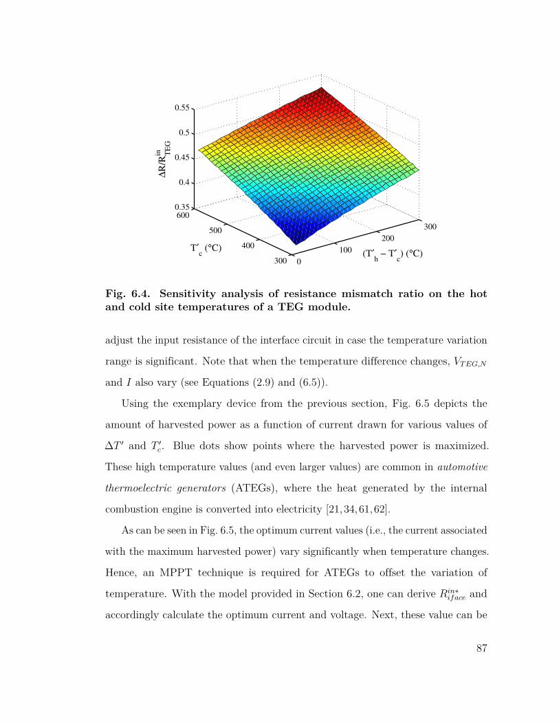
0
100
200
300
300
400
500
6000.35
0.4
0.45
0.5
0.55
(T′h − T′
c) (°C)
T′c (°C)
∆R
/RT
EG
in
Fig. 6.4. Sensitivity analysis of resistance mismatch ratio on the hotand cold site temperatures of a TEG module.
adjust the input resistance of the interface circuit in case the temperature variation
range is significant. Note that when the temperature difference changes, 𝑉𝑇 𝐸𝐺,𝑁
and 𝐼 also vary (see Equations (2.9) and (6.5)).
Using the exemplary device from the previous section, Fig. 6.5 depicts the
amount of harvested power as a function of current drawn for various values of
Δ𝑇 ′ and 𝑇 ′𝑐. Blue dots show points where the harvested power is maximized.
These high temperature values (and even larger values) are common in automotive
thermoelectric generators (ATEGs), where the heat generated by the internal
combustion engine is converted into electricity [21,34,61,62].
As can be seen in Fig. 6.5, the optimum current values (i.e., the current associated
with the maximum harvested power) vary significantly when temperature changes.
Hence, an MPPT technique is required for ATEGs to offset the variation of
temperature. With the model provided in Section 6.2, one can derive 𝑅𝑖𝑛*𝑖𝑓𝑎𝑐𝑒 and
accordingly calculate the optimum current and voltage. Next, these value can be
87
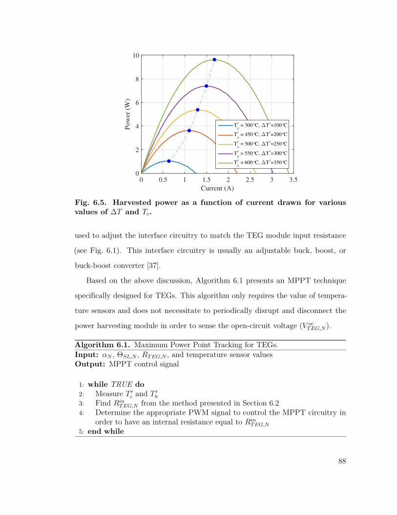
Current (A)
0 0.5 1 1.5 2 2.5 3 3.5
Pow
er
(W)
0
2
4
6
8
10
T′
c = 300°C, ∆T
′=100°C
T′
c = 450°C, ∆T
′=200°C
T′
c = 500°C, ∆T
′=250°C
T′
c = 550°C, ∆T
′=300°C
T′
c = 600°C, ∆T
′=350°C
Fig. 6.5. Harvested power as a function of current drawn for variousvalues of Δ𝑇 and 𝑇𝑐.
used to adjust the interface circuitry to match the TEG module input resistance
(see Fig. 6.1). This interface circuitry is usually an adjustable buck, boost, or
buck-boost converter [37].
Based on the above discussion, Algorithm 6.1 presents an MPPT technique
specifically designed for TEGs. This algorithm only requires the value of tempera-
ture sensors and does not necessitate to periodically disrupt and disconnect the
power harvesting module in order to sense the open-circuit voltage (𝑉 𝑜𝑐𝑇 𝐸𝐺,𝑁).
Algorithm 6.1. Maximum Power Point Tracking for TEGs.Input: 𝛼𝑁 , Θ𝑆𝐿,𝑁 , 𝑅𝑇 𝐸𝐺,𝑁 , and temperature sensor valuesOutput: MPPT control signal
1: while TRUE do2: Measure 𝑇 ′
𝑐 and 𝑇 ′ℎ
3: Find 𝑅𝑖𝑛𝑇 𝐸𝐺,𝑁 from the method presented in Section 6.2
4: Determine the appropriate PWM signal to control the MPPT circuitry inorder to have an internal resistance equal to 𝑅𝑖𝑛
𝑇 𝐸𝐺,𝑁
5: end while
88
The proposed algorithm comprises of a control loop (line 1 to 5) where it
periodically senses 𝑇 ′𝑐 and 𝑇 ′
ℎ (line 2). Note that 𝑇𝑐 and 𝑇ℎ values cannot be sensed
directly. Accordingly, it finds the internal resistance of the TEG module (line 3).
Knowing the value of the internal resistance, a controlling PWM signal can be
generated to adjust 𝑅𝑖𝑛𝑖𝑓𝑎𝑐𝑒 of the interface circuitry to be equal to 𝑅𝑖𝑛
𝑇 𝐸𝐺,𝑁 (line 4).
Details of the last step is outside the scope of this dissertation and can be found in
the literature.
6.5 Summary
In this chapter, it was analytically shown that the effective internal resistance
of TEGs can vary from its electrical resistance by more than 50%. This difference
comes from ignoring the dependence of the electrical behavior of TEG on its thermal
behavior. Accordingly, a systematic method for accurately determining the TEG
input resistance was developed. Based on this method, a maximum power point
tracking algorithm was presented to offset the effect of temperature variation on
the input resistance.
89
Part II
Techniques Targeting Mobile
Systems
90
7Background and Prior Work
7.1 Background
Compact thermal modeling is a popular technique for simulating the thermal
behavior of a system comprised of various components. This subsection explains
how the compact thermal model (CTM) of a system is built. Due to the duality of
thermal and electrical phenomena, an equivalent RC network can be constructed
from a CTM. Finding the voltage of every node in this RC network is equivalent to
deriving the temperature of sub-components in the initial system model.
To build a CTM of a physical object, its components should be divided into
sub-components with smaller dimensions. Finer granularity of sub-component
division helps to produce more accurate temperature maps at the cost of increased
runtime and memory usage. Each sub-component is modeled as a node in the
thermal RC network and has a single temperature value. A thermal resistance
is calculated for every sub-component pairs in contact, based on their material
properties, dimensions, and the contact area. Similarly, a capacitance is added
between every node and the ground. This capacitance captures the sub-component
specific heat.
Fig. 7.1 shows a small part of a thermal RC network for the Qualcomm MSM8660
91
Mobile Developer Platform (MDP) (see [63] for details on MDP devices). The
components in Fig. 7.1, from top to bottom, include screen protector, display
module, PCB, IC chips, battery, and rear case. Various components can be broken
into non-equal number of sub-components according to their importance and
requirements of solution quality. For two adjacent sub-components 𝑖 and 𝑗, the
thermal resistance is calculated by serially connecting two thermal resistors from
their centers to the shared surface as follows.
𝑟𝑖,𝑗 = 𝑟𝑗,𝑖 = 𝑟𝑖 + 𝑟𝑗 = 1𝐴𝑖,𝑗
( 𝑡𝑖
𝑔𝑖
+ 𝑡𝑗
𝑔𝑗
), (7.1)
where 𝐴𝑖,𝑗 is the common area between these two contacted sub-components, 𝑔𝑖
and 𝑔𝑗 are thermal conductivities of their respective sub-components, and 𝑡𝑖 and
𝑡𝑗 are the perpendicular distances from the center of sub-components 𝑖 and 𝑗 to
the shared surface, respectively. Note that any adjacency between sub-components
are detected in a 3D space and thereby, orthotropic thermal conductivity should
be considered. A material is orthotropic if its thermal conductivity varies in
different directions. PCBs are a good examples of orthotropic materials; they have
copper traces spanned in the horizontal plane and hence exhibit a higher thermal
conductivity in that direction compared to the vertical direction.
At the boundaries of a device, heat diffuses to the ambient environment (i.e.,
air). Thus, the boundary thermal resistance between the 𝑖th sub-component and
the ambient air is calculated as,
𝑟𝑖,𝑎𝑚𝑏 = 𝑟𝑖 + 𝑟𝑎𝑚𝑏 = 1𝐴𝑖,𝑎𝑚𝑏
( 𝑡𝑖
𝑔𝑖
+ 1ℎ𝑎𝑖𝑟
), (7.2)
where ℎ𝑎𝑖𝑟 is the air heat transfer coefficient. In the natural convection condition,
ℎ𝑎𝑖𝑟 has the value of 5∼25 W/(m2 ·K) [64].
92
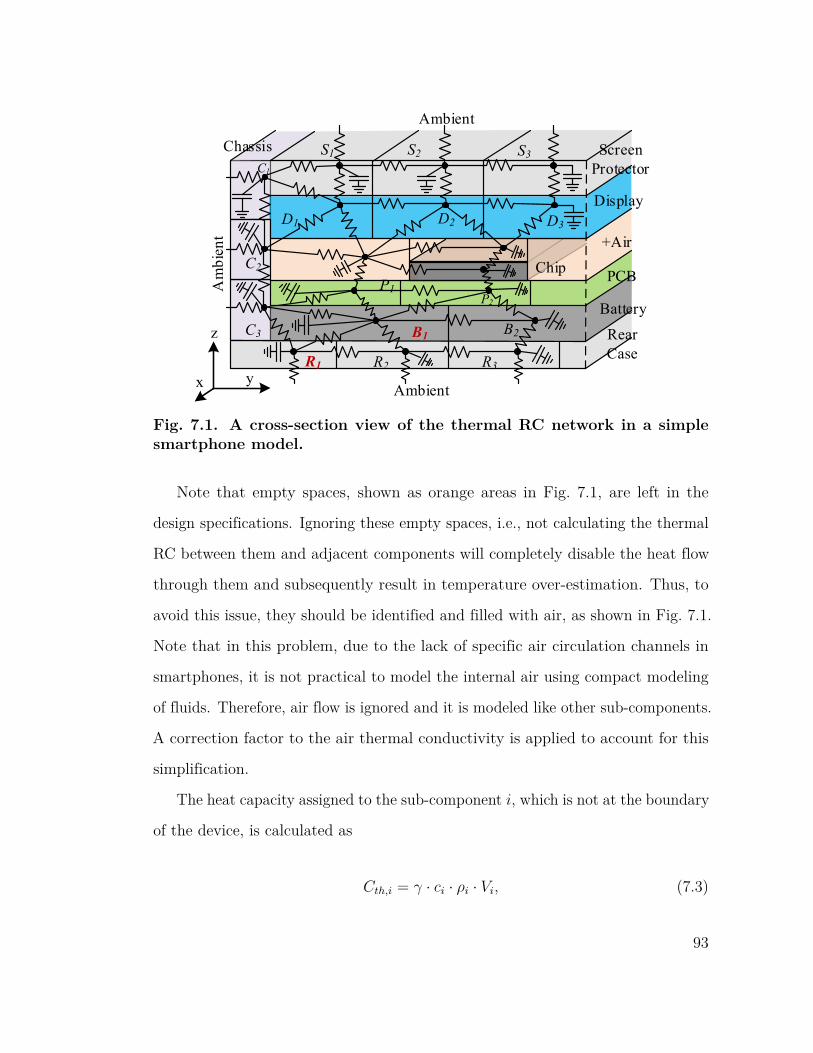
Display
+AirChip PCB
ChassisC1
C2
D1 D2 D3
P1P2
ScreenProtector
C3Battery
Rear Case
B1 B2
R1 R2 R3
S1 S2 S3
z
y
Ambient
Ambient
Am
bien
t
x
Fig. 7.1. A cross-section view of the thermal RC network in a simplesmartphone model.
Note that empty spaces, shown as orange areas in Fig. 7.1, are left in the
design specifications. Ignoring these empty spaces, i.e., not calculating the thermal
RC between them and adjacent components will completely disable the heat flow
through them and subsequently result in temperature over-estimation. Thus, to
avoid this issue, they should be identified and filled with air, as shown in Fig. 7.1.
Note that in this problem, due to the lack of specific air circulation channels in
smartphones, it is not practical to model the internal air using compact modeling
of fluids. Therefore, air flow is ignored and it is modeled like other sub-components.
A correction factor to the air thermal conductivity is applied to account for this
simplification.
The heat capacity assigned to the sub-component 𝑖, which is not at the boundary
of the device, is calculated as
𝐶𝑡ℎ,𝑖 = 𝛾 · 𝑐𝑖 · 𝜌𝑖 · 𝑉𝑖, (7.3)
93
where 𝛾 is a correction factor, whereas 𝑐𝑖, 𝜌𝑖, and 𝑉𝑖 are the specific heat, the
density, and the volume of sub-component 𝑖. 𝛾 is determined empirically as 0.5 to
offset the effect of lumping capacitors. If the 𝑖th component is at the boundary of
the device, its heat capacity is calculated as
𝐶𝑡ℎ,𝑖 = 𝛾(︁𝑐𝑖 · 𝜌𝑖 · 𝑉𝑖 + 𝐶𝑐𝑜𝑛𝑣
𝑡ℎ,� · 𝐴𝑖,𝑎𝑚𝑏
)︁, (7.4)
where 𝐶𝑐𝑜𝑛𝑣𝑡ℎ,� is the convection heat capacitance per unit area and 𝐴𝑖,𝑎𝑚𝑏 is the
common area between the sub-component 𝑖 and the ambient.
The ambience is modeled using a constant voltage source with the value of the
ambient temperature. This voltage source is connected to the nodes corresponding to
the sub-components at the boundary of the device. Power generation of components
is modeled using current sources.
By nodal analysis of the CTM RC network, one can derive
𝐶𝑑𝑇 (𝑡)
𝑑𝑡+ 𝐺𝑇 (𝑡) = 𝑃 (𝑡), (7.5)
where 𝑡 is time, 𝐶 is the thermal capacitance matrix, 𝑇 is the temperature vector
at time 𝑡, 𝐺 is the conductance matrix, and 𝑃 is the power consumption vector at
time 𝑡. 𝐶 is a diagonal matrix; each element on the main diagonal represents the
heat capacity of its corresponding sub-component. 𝐺 can be represented as
𝐺 =
⎡⎢⎢⎢⎢⎢⎢⎢⎢⎢⎣
∑︀𝑖 𝑔1,𝑖 −𝑔1,2 . . . −𝑔1,𝑛
−𝑔2,1∑︀
𝑖 𝑔2,𝑖 . . . −𝑔2,𝑛
... ... . . . ...
−𝑔𝑛,1 −𝑔𝑛,2 . . .∑︀
𝑖 𝑔𝑛,𝑖
⎤⎥⎥⎥⎥⎥⎥⎥⎥⎥⎦, (7.6)
94
where 𝑔𝑖,𝑗 represents the thermal conductivity between sub-components 𝑖 and 𝑗.
Clearly, the following relation holds.
𝑔𝑖,𝑗 = 𝑔𝑗,𝑖 = 1𝑟𝑖,𝑗
= 1𝑟𝑗,𝑖
(7.7)
In the steady-state thermal analysis, similar to the DC analysis of RC circuits,
the first term in Eq. (7.5) is dropped and the resultant system of linear equations
is solved. On the other hand, for transient analysis, the entire Eq. (7.5), which
forms a system of ordinary differential equations (ODEs), is solved. This is a
nonhomogeneous, first-order linear system of ODEs, which has the following closed-
form solution [65],
𝑇 (𝑡) = 𝑒−𝑌 𝑡(︂∫︁ 𝑡
𝑡0𝑒𝑌 𝑡𝑋(𝑡)𝑑𝑡 + 𝑇 (𝑡0)
)︂, (7.8)
where 𝑋(𝑡)=𝐶−1𝑃 (𝑡) and 𝑌 =𝐶−1𝐺. Calculating the numerical value of this solu-
tion is comprised of matrix exponentials and hence, requires numerical estimation
of power series. Moreover, 𝑃 (𝑡) is given over some period of time (say from 𝑡 to
𝑡 + Δ𝑡) and hence, the integral is converted into a summation. As a result, Eq. (7.8)
should be solved using numerical methods. In Chapter 8, it is demonstrated that
how Therminator 2 solves this equation.
7.2 Prior Work
7.2.1 Thermal Simulation
HotSpot [19] is a successful early-stage CTM-based simulation tool targeting
thermal analysis of a silicon die and its packaging which are cooled with a heat sink
95
and possibly a fan. It is capable of generating die temperature maps. Temptor [66] is
a tool based on HotSpot which allows the temperature prediction using performance
counters instead of components’ power trace. Meng et al. [67] improved HotSpot by
adding the 3D chip simulation support. 3D-ICE [68] is another thermal simulator
targeting 3D ICs equipped with liquid cooling. However, neither HotSpot nor
3D-ICE can be modified or extended to analyze small form-factor devices as they
target a single IC package along with its cooling equipment. In fact, modeling
smartphone is much more complicated due to the following reasons:
1. Multiple heat generators, including battery, display, and a number of IC
chips.
2. Complex 3D layout where each component may be in vertical and/or horizontal
contact with several other components.
3. Necessity of considering the internal air in the device.
Comparing to those tools, Therminator 2 (introduced in Chapter 8) focuses on
component-level thermal modeling, in which the architecture-level details inside a
single chip package are ignored. Besides, Therminator 2 can be used for realtime
(online) simulations. I have shown in Chapter 9 that given the average power
consumption of active components of the device every second, Therminator 2 can
produce respective temperature maps at the same rate.
Several researches have been conducted in studying the thermal design for
smartphones and tablets. Luo et al. [69] established a simple thermal resistance
network to analyze the whole mobile phone system. However, the thermal resistance
network built in [69] is oversimplified as each component is modeled as one block
with a single uniform temperature value. Gurrum et al. [70] modeled the smartphone
in CFD tools and analyzed the thermal effect of using materials with different
96
thermal conductivities through CFD simulation. Rajmond and Fodor [71] used
CFD tools to show that attaching thermal pad on top of the AP significantly
reduces the AP temperature. To the best of my knowledge, Therminator 2 (and its
earlier version) is the first tool targeting smartphones that automatically builds a
compact thermal model from the device specifications, and solves for temperature
maps of all components accurately.
7.2.2 Smartphone Power Characterization
Many efforts have been conducted on the power characterization, modeling, and
metering of portable devices without direct measurement. All of these efforts can be
classified into two main categories. First, sampling techniques (e.g., PowerTutor [72],
Sesame [73], and [74]), which rely on polling the device internal sensors, hardware
performance counters, OS kernel sysfs/procfs contents, or the battery sensors.
Second, event-driven methods (e.g., eprof [75], AppScope [76], and FEPMA [77])
in which the OS kernel is properly instrumented to report desired events (usually
component-level activity information and power state transitions). It is shown in [76]
that event-driven methods have lower overhead and higher accuracy compared
to sampling techniques. Moreover, it is demonstrated in [77] that event-driven
methods can capture high-frequency power change events, whereas the first method
lacks this capability.
I found that the CPU model characterized in AppScope was single-core and
in FEPMA was dual-core. In Chapter 9, I model a quad-core processor and
consider the power correlation among the cores. Moreover, GPU model is missing
in AppScope [76] and is modeled in FEPMA [77] using an artificial neural network
which captures the dependence between the CPU workload and that of the GPU.
This approach imposes a significant computational load for the power calculator and
97
its accuracy should be improved by direct modeling. Besides, it does not consider
the effect of frequency scaling on GPU power. Furthermore, FEPMA cannot reveal
which application/process is accessing GPU. In contrast, PowerTap (introduced in
Chapter 9) directly models the GPU power, which is fast and more accurate. Last
but not least, PowerTap considers the internal flash storage of the device, which
consumes substantial power (∼0.6 W) during disk intensive operations.
98
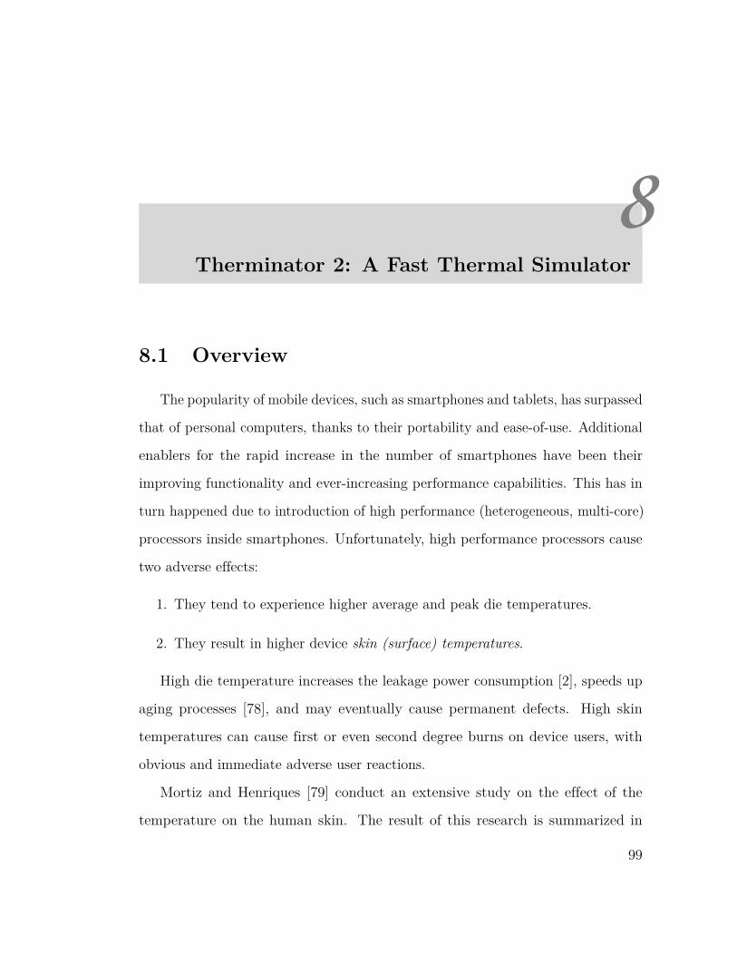
8Therminator 2: A Fast Thermal Simulator
8.1 Overview
The popularity of mobile devices, such as smartphones and tablets, has surpassed
that of personal computers, thanks to their portability and ease-of-use. Additional
enablers for the rapid increase in the number of smartphones have been their
improving functionality and ever-increasing performance capabilities. This has in
turn happened due to introduction of high performance (heterogeneous, multi-core)
processors inside smartphones. Unfortunately, high performance processors cause
two adverse effects:
1. They tend to experience higher average and peak die temperatures.
2. They result in higher device skin (surface) temperatures.
High die temperature increases the leakage power consumption [2], speeds up
aging processes [78], and may eventually cause permanent defects. High skin
temperatures can cause first or even second degree burns on device users, with
obvious and immediate adverse user reactions.
Mortiz and Henriques [79] conduct an extensive study on the effect of the
temperature on the human skin. The result of this research is summarized in
99
Fig. 8.1. This figure shows that the required time to cause a burn (first or second
degree) decays exponentially as the temperature increases. These data are collected
for adults and it is expected that burn occurs faster for children and old people. It
is also reported that the maximum safe temperature for the human skin is about
45 ∘C. This threshold has also been confirmed by other researchers [80,81].
1
10
100
1,000
10,000
47 49 50 52 55 60 65 68
Expo
sure
Tim
e (s
ec)
Temperature (˚C)
1st Degree Burn
2nd Degree Burn
Fig. 8.1. Estimated exposure time of the human skin to the hot waterin order to result in a burn.
Hence, thermal design (i.e., designing the heat flow path and a cooling method)
and thermal management (i.e., employing thermal response mechanisms to avoid
hot spots and high die temperatures) are crucial for a mobile device to improve its
performance and energy efficiency while maintaining safe temperatures.
Proper thermal design effectively removes heat away from a VLSI circuit die. In
smartphones, application processors (APs) incorporate CPU, GPU, DSP, sometimes
a baseband radio unit, and so on. The AP is a major heat generator in smartphones
[70]. Due to the cost, form factor, noise, and safety issues, smartphones rely on
passive cooling methods that dissipate the heat generated by the AP through
thermal conduction to the device skin. Thermal pads are usually attached on top
of the AP chip package to ease the heat removal [70, 71]. Thermal management
100
techniques, such as frequency throttling and voltage/frequency scaling, are also
exploited to avoid high die temperatures. For example, one can observe that
the CPU and GPU performance (and consequently their power consumption) are
throttled in Samsung Exynos 5250 so as to prevent the AP’s junction temperature
from exceeding an upper threshold [82].
As noted above, thermal design and management of smartphones are also
concerned a skin temperature constraint. This constraint refers to the fact that
the temperature at the device skin must not exceed a certain threshold. Ideally,
distributing the heat uniformly onto the device skin results in the most effective heat
dissipation. However, in practice, majority of the heat flows in vertical direction
from the AP die, and thus hot spots are formed on the device skin above the AP
location [83]. It is reported that the hottest spot on Apple iPad 3 can reach as high
as 47 ∘C while playing graphic intensive games [84]. Usually, a skin temperature
thermal governor is implemented to maintain the skin temperature at a desired
setpoint by using a control feedback.
To address this design challenge, it is necessary to model the temperature map
(i.e., temperature gradients) for the smartphone in an accurate and efficient manner.
Knowing the detailed temperature map on the device skin at the design time is
helpful in the device fabrication. For example, using materials with high thermal
conductivity in the thermal path enhances heat removal from the AP and in turn
causes high skin temperature, whereas using low thermal conductivity materials
cannot remove the heat from the AP fast enough and hence the die temperature
goes up. Moreover, knowing how the temperature of a particular component
depends on use cases helps to derive the optimal thermal management policy for
that component. For instance, setting CPU frequency throttling threshold(s) is
affected by how skin temperature depends on the CPU frequency.
101
Analyzing temperature maps at early stages of the design flow can significantly
reduce the design time. Even though computational fluid dynamics (CFD) tools
generate accurate temperature maps, they are expensive and not compatible with
other performance/power simulators. As explained in Chapter 7, the compact
thermal modeling(CTM) method is used for thermal analysis with reasonable
accuracy and low computational complexity [19,85].
In this chapter, a CTM-based component-level thermal simulator called Ther-
minator 2 is presented. Therminator 2 (along with its earlier version [19]) is
the first thermal simulator that targets small form-factor mobile devices (such
as smartphones and tablets). It produces temperature maps for all components,
including the AP, battery, display, and other key device components, as well as
the skin of the device, with high accuracy and fast runtime. Therminator 2 results
have been validated against thermocouple measurements on a Qualcomm Mobile
Developer Platform (MDP) [63] and simulation results generated by Autodesk Sim-
ulation CFD [86]. It is very versatile in handling different device specifications and
component usage information, which allows a user to explore impacts of different
thermal designs and thermal management policies. New devices can be simply
described through an input specification file (in XML format). A detailed case
study has been conducted for Samsung Galaxy S4 by using Therminator 2. The
temperature results relate the device performance to the device skin temperature,
as well as the impact of the thermal path design.
The new contributions of Therminator 2 compared to the earlier version [19]
are listed below:
1. Adding the capability of fast transient-state thermal simulations. The accu-
racy of simulation results are verified through measurements performed on a
Google Nexus 5 device.
102
2. Exploiting the power of parallel processing on multi-core CPUs to reduce
the runtime by more than 27x for steady-state thermal simulations and to
perform the transient-state simulations in real-time.
The rest of this chapter is organized as follows. Section 8.2 introduces the
Therminator 2 architecture. Next, Section 8.3 describes techniques used to solve
thermal equations. After that, Section 8.4 elaborates implementation details and
the evaluation of Therminator 2. A case study is provided in Section 8.5. Finally,
Section 8.6 summarizes the chapter.
8.2 Therminator 2 Architecture
Fig. 8.2 depicts how Therminator 2 works. It takes two input files provided by a
user. The specs.xml file describes the smartphone design, including components
of interest, their geometric dimensions (length, width, and thickness), and relative
positions. Users should provide properties of materials (i.e., thermal conductivity,
density, and specific heat) used to manufacture the described device through this
file. The power.trace file provides the power consumption of active components
that generate heat, e.g., ICs, the battery, and the display. The power trace of each
component can be obtained through real measurements or other power estimation
tools/methods such as [20, 49, 72]. power.trace is provided as a separate file so
that one can easily interface a performance/power simulator (such as GEM5/McPat
[49, 87]) with Therminator 2.
Therminator 2 has three main modules. A parser module parses input files,
updates the material library, and makes a set comprised of components specified by
the input file. Moreover, it performs multiple sanity checks to detect discrepancy
among specified components, e.g., positions of two components which are set such
103
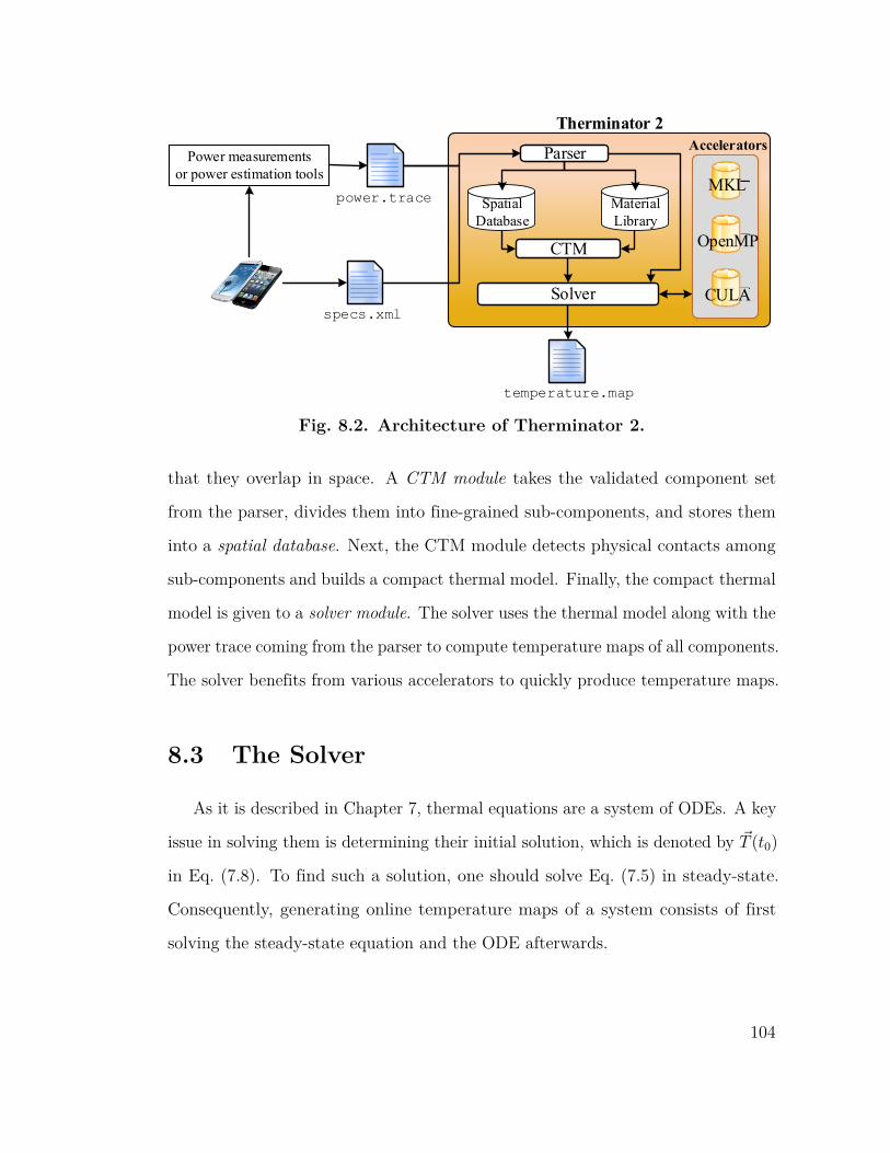
Accelerators
temperature.map
Therminator 2
Parser
specs.xml
SpatialDatabase
MaterialLibrary
power.trace
Power measurements or power estimation tools
CTM
MKL
OpenMP
CULA Solver
Fig. 8.2. Architecture of Therminator 2.
that they overlap in space. A CTM module takes the validated component set
from the parser, divides them into fine-grained sub-components, and stores them
into a spatial database. Next, the CTM module detects physical contacts among
sub-components and builds a compact thermal model. Finally, the compact thermal
model is given to a solver module. The solver uses the thermal model along with the
power trace coming from the parser to compute temperature maps of all components.
The solver benefits from various accelerators to quickly produce temperature maps.
8.3 The Solver
As it is described in Chapter 7, thermal equations are a system of ODEs. A key
issue in solving them is determining their initial solution, which is denoted by 𝑇 (𝑡0)
in Eq. (7.8). To find such a solution, one should solve Eq. (7.5) in steady-state.
Consequently, generating online temperature maps of a system consists of first
solving the steady-state equation and the ODE afterwards.
104
8.3.1 Steady-State Analysis
In this section, two techniques for solving Eq. (7.5) in steady state are investi-
gated. In other words, the aim is to solve the following set of linear equations.
𝐺𝑇 (𝑡) = 𝑃 (𝑡) (8.1)
The first technique is the LUP decomposition, which is used in the initial version
of Therminator, and the second method is the Cholesky decomposition, which is
much faster and employed in Therminator 2.
8.3.1.1 LUP Decomposition
The LUP decomposition method decomposes 𝐺 into a lower and upper triangular
matrices, and then applies forward and backward substitution to solve Eq. (8.1)
for 𝑇 (𝑡). Matrix solving techniques, namely, the LUP decomposition method
followed by the forward and backward substitution method, are implemented using
a sequential method (which utilizes a single core of a CPU) and a parallel method
(which utilizes the GPU), respectively. For the parallel method, Therminator adopts
CULA Dense [88], which is a set of GPU-accelerated linear algebra libraries utilizing
the NVIDIA CUDA parallel computing platform. One can observe that the parallel
method speeds up Therminator by more than two orders of magnitude against
the sequential method, as shown in Fig. 8.3. Runtime results of both methods are
measured on a server with 4×Intel Xeon E7-8837 CPUs, 64 GB of memory, and an
NVIDIA Quadro K5000 GPU.
105
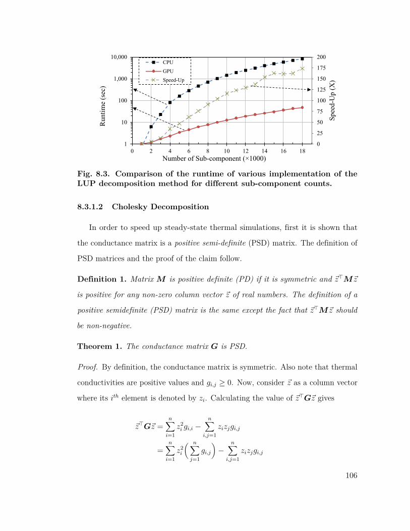
0
25
50
75
100
125
150
175
200
1
10
100
1,000
10,000
0 2 4 6 8 10 12 14 16 18
Spee
d-U
p (X
)
Run
time
(sec
)
Number of Sub-component (×1000)
CPUGPUSpeed-Up
Fig. 8.3. Comparison of the runtime of various implementation of theLUP decomposition method for different sub-component counts.
8.3.1.2 Cholesky Decomposition
In order to speed up steady-state thermal simulations, first it is shown that
the conductance matrix is a positive semi-definite (PSD) matrix. The definition of
PSD matrices and the proof of the claim follow.
Definition 1. Matrix 𝑀 is positive definite (PD) if it is symmetric and �⃗�⊤𝑀 �⃗�
is positive for any non-zero column vector �⃗� of real numbers. The definition of a
positive semidefinite (PSD) matrix is the same except the fact that �⃗�⊤𝑀 �⃗� should
be non-negative.
Theorem 1. The conductance matrix 𝐺 is PSD.
Proof. By definition, the conductance matrix is symmetric. Also note that thermal
conductivities are positive values and 𝑔𝑖,𝑗 ≥ 0. Now, consider �⃗� as a column vector
where its 𝑖𝑡ℎ element is denoted by 𝑧𝑖. Calculating the value of �⃗�⊤𝐺�⃗� gives
�⃗�⊤𝐺�⃗� =𝑛∑︁
𝑖=1𝑧2
𝑖 𝑔𝑖,𝑖 −𝑛∑︁
𝑖,𝑗=1𝑧𝑖𝑧𝑗𝑔𝑖,𝑗
=𝑛∑︁
𝑖=1𝑧2
𝑖
(︂ 𝑛∑︁𝑗=1
𝑔𝑖,𝑗
)︂−
𝑛∑︁𝑖,𝑗=1
𝑧𝑖𝑧𝑗𝑔𝑖,𝑗
106
=𝑛∑︁
𝑖,𝑗=1𝑧2
𝑖 𝑔𝑖,𝑗 −𝑛∑︁
𝑖,𝑗=1𝑧𝑖𝑧𝑗𝑔𝑖,𝑗
= 12
(︂ 𝑛∑︁𝑖,𝑗=1
(𝑧2𝑖 𝑔𝑖,𝑗 + 𝑧2
𝑗 𝑔𝑗,𝑖)− 2𝑛∑︁
𝑖,𝑗=1𝑧𝑖𝑧𝑗𝑔𝑖,𝑗
)︂
= 12
(︂ 𝑛∑︁𝑖,𝑗=1
(𝑧2𝑖 + 𝑧2
𝑗 )𝑔𝑖,𝑗 − 2𝑛∑︁
𝑖,𝑗=1𝑧𝑖𝑧𝑗𝑔𝑖,𝑗
)︂
= 12
𝑛∑︁𝑖,𝑗=1
(𝑧𝑖 − 𝑧𝑗)2𝑔𝑖,𝑗 ≥ 0.
Hence, 𝐺 is PSD.
Next, the conductance matrix is transformed into a positive definite matrix,
which allows Cholesky decomposition to be used in order to solve Eq. (8.1). On the
other hand, note that the LUP decomposition is a generic matrix decomposition
technique that can be applied to any matrix. Therminator 2 uses the Cholesky
decomposition which is proven to be much faster than the LUP decomposition [89].
In order to apply the Cholesky decomposition on a matrix, the matrix should
be PD. The technique explained in [89] is employed in order to apply the Cholesky
decomposition technique to a PSD matrix as explained next. Consider a matrix
called 𝐺𝑘 = 𝐺 + (1/𝑘)𝐼, where 𝐼 is the identity matrix and 𝑘 is a large positive
value. Using the same argument presented in the proof of Theorem 1, it can be seen
that 𝐺𝑘 is PD. Moreover, the value of 𝑘 can be chosen arbitrarily large such that
𝐺𝑘 becomes an approximation of 𝐺. As a result, it can be seen that matrix 𝐺𝑘 can
be decomposed to 𝐿𝑘𝐿⊤𝑘 , where 𝐿𝑘 is a lower triangular matrix. As 𝑘 approaches
to infinity, 𝐿𝑘𝐿⊤𝑘 tends to 𝐿𝐿⊤, which is the decomposition of matrix 𝐺. A very
large 𝑘 is chosen to calculate the Cholesky decomposition of 𝐺 numerically with
negligible loss of accuracy (less than 10−4 ∘C).
Moreover, it is shown that the conductance matrix is sparse and hence the
sparse variant of Cholesky decomposition may be used to achieve further speed-up.
107
The definition of a sparse matrix and the proof of the claim are as follows.
Definition 2. An 𝑛 × 𝑛 matrix is sparse, if at most 𝒪(𝑛) of its elements are
non-zero [90].
Theorem 2. The conductance matrix 𝐺 is sparse.
Proof. Every row of the conductance matrix corresponds to a sub-component
in the CTM. When the sub-components are small enough, they have only six
neighbors (i.e., only a sub-component resides at each side of a rectangular cuboid).
Considering the diagonal elements, there are seven non-zero elements in every row
of the conductance matrix. Hence, the conductance matrix has a total of 7𝑛 = 𝒪(𝑛)
non-zero elements.
Finally, note that Therminator 2 adopts the parallelized version of the sparse
Cholesky decomposition to achieve even more speed-up. Fig. 8.4 compares the
runtime of Therminator 2 executed on an Intel Core-i7 3770 3.4GHz with the initial
version of Therminator which utilizes NVIDIA Quadro K5000. As can be seen,
Therminator 2 running on a $300 CPU beats the first release of Therminator which
takes advantage of a $1,800 GPU by about 27x for large number of sub-components.
The speed-up for small number of sub-components (about 1,000 sub-components)
is very large (over 200x), which is due to the initial overhead of setting up GPU.
Moreover, note that the Therminator 2 runtime is below 0.35 seconds for very large
sub-component counts.
8.3.2 Transient Analysis
Based on various experiments, it is observed that the ODE presented in Eq. (7.5)
is stiff, which means that numerical methods for solving it are unstable, unless the
step size in solving the ODE is selected to be extremely small [91]. Hence, there
108
Therminator 2
Fig. 8.4. Runtime comparison between Therminator and Therminator 2for different number of components.
are two issues in solving this ODE. First, the step sizes should be carefully selected
to avoid any divergence. Second, selecting very small steps in solving ODE results
in a very slow solver.
To address the first issue, Runge-Kutta method is adopted with adaptive steps,
where the steps are chosen by the 5th-order Dormand-Prince technique. This
technique is shown to handle stiff equations properly [91].
To address the second issue, it turned out that the main procedure which is in
charge of numerically calculating 𝑑𝑇𝑑𝑡
is the bottleneck because it is called multiple
times per each step. Three avenues are taken to speed up this main procedure.
First, 𝑌 is pre-calculated and 𝑋 is only calculated when 𝑃 (𝑡) changes. Next, it
is noted that 𝑌 is sparse. The reason is as follows. Remember the fact that 𝐺
was proven to be sparse. 𝑌 is formed by multiplying a diagonal matrix (i.e., 𝐶−1)
to 𝐺 and hence the resultant remains sparse. This sparsity reduces unnecessary
computations significantly. Last but not least, the main procedure is parallelized
such that the value of 𝑑𝑇𝑑𝑡
for every row of this vector is calculated in parallel.
109
Unfortunately, a fair comparison between transient-state solvers of Thermina-
tor 2 and HotSpot was not possible because it turned out that it took a few hours
for HotSpot’s solver to simulate one second of thermal change and sometimes, the
solution diverges. Hence no comparison is provided here. On the desktop CPU
detailed in the previous subsection, Therminator 2 manages to solve an ODE for one
second in realtime (in one wall-clock second) when the number of sub-components
is about 3,500.
8.4 Implementation & Evaluation
8.4.1 Implementation
Therminator 2 is implemented using C++ and compiled by GCC 4.9. The
parser adopts PugiXML [92], an open source, light-weight, and fast C++ XML
processing library. The built-in material library is a class called Materials which
holds default material properties and its data are updated by the parser. All
components and sub-components are instances of Component and Subcomponent
classes, respectively. A Device class keeps track of sub-component objects using a
spatial database. Another class called Model takes the device object and builds the
thermal model based on Equations (7.1)-(7.4). Several geometric utility methods
are implemented in order to perform basic spatial queries on sub-components, e.g.,
checking the physical contact between every two sub-components, determining if
they have overlap in space, and calculating their common area. Moreover, the
Model class calls another parser to read the power.trace file which contains the
power consumption of each component.
As explained previously, Therminator 2 requires to exploit the system’s max-
imum performance. Hence, C++ is selected for its implementation. Besides,
110
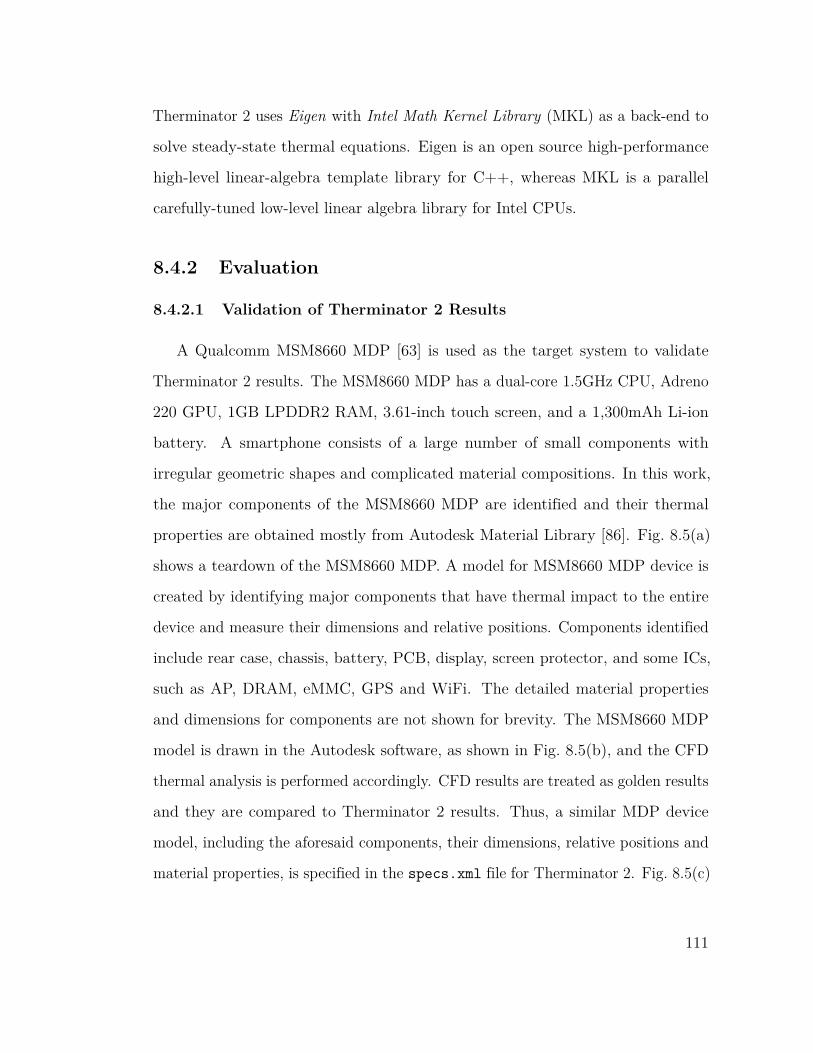
Therminator 2 uses Eigen with Intel Math Kernel Library (MKL) as a back-end to
solve steady-state thermal equations. Eigen is an open source high-performance
high-level linear-algebra template library for C++, whereas MKL is a parallel
carefully-tuned low-level linear algebra library for Intel CPUs.
8.4.2 Evaluation
8.4.2.1 Validation of Therminator 2 Results
A Qualcomm MSM8660 MDP [63] is used as the target system to validate
Therminator 2 results. The MSM8660 MDP has a dual-core 1.5GHz CPU, Adreno
220 GPU, 1GB LPDDR2 RAM, 3.61-inch touch screen, and a 1,300mAh Li-ion
battery. A smartphone consists of a large number of small components with
irregular geometric shapes and complicated material compositions. In this work,
the major components of the MSM8660 MDP are identified and their thermal
properties are obtained mostly from Autodesk Material Library [86]. Fig. 8.5(a)
shows a teardown of the MSM8660 MDP. A model for MSM8660 MDP device is
created by identifying major components that have thermal impact to the entire
device and measure their dimensions and relative positions. Components identified
include rear case, chassis, battery, PCB, display, screen protector, and some ICs,
such as AP, DRAM, eMMC, GPS and WiFi. The detailed material properties
and dimensions for components are not shown for brevity. The MSM8660 MDP
model is drawn in the Autodesk software, as shown in Fig. 8.5(b), and the CFD
thermal analysis is performed accordingly. CFD results are treated as golden results
and they are compared to Therminator 2 results. Thus, a similar MDP device
model, including the aforesaid components, their dimensions, relative positions and
material properties, is specified in the specs.xml file for Therminator 2. Fig. 8.5(c)
111
visualizes the 3D layout model that Therminator 2 creates from the input file. Note
that Therminator 2 applies different granularity to various components.
AP LCDDisplay
Chassis
Battery
Rear Case
PCB
Thermocouples
ScreenProtector
Temperature measurement point
Thermometer
(a)
APBattery
PCB
LCD Display
Screen ProtectorChassis
Rear Case
(b) (c)
Fig. 8.5. (a) Teardown of MSM8660 MDP device and temperaturemeasurement kits (circle marks are temperature measurement points.Note for the PCB, thermocouple is attached onto the other side), (b)CFD drawing, and (c) Therminator 2 3D visualization.
A few representative use cases are executed that utilize different components and
consume various amounts of power. Use cases tested in this work are StabilityTest
(an application that heavily stresses CPU, GPU, and the memory [93]), Candy Crush
(a popular mobile game [94]), YouTube (a famous video streaming application [95]),
the built-in camcorder application, and a local video playback. Trepn Profiler [96]
112
is adopted to record the per-component power consumption breakdown of this
device, and provide the results as inputs to both CFD simulation software and
Therminator 2. Note that the total power consumption of some small components
(interconnects, sensors, etc.) is assigned to the PCB uniformly because the schematic
diagram of the MSM8660 MDP is not available to precisely locate them.
Thermocouples are used to measure temperatures at three locations in MSM8660
MDP, shown as red circles in Fig. 8.5(a). Temperatures are measured at three
different locations:
1. The hot spot on the screen located above the AP;
2. The hot spot on the rear case located below the battery (because there is a
big air gap between the PCB and the rear case, the hot spot on the rear case
is located below the battery); and
3. The PCB (the opposite side of the board shown in Fig. 8.5(a)).
The ambient temperature is measured as 23.0 ∘C during the experiments. Sysfs of
the MDP device is accessed through the Android Debug Bridge (ADB) interface
and the AP junction temperature is obtained by reading the temperature register
in the /sys/class/thermal/thermal_zone2 directory. Note that the temperature
register has the accuracy of ±1 ∘C.
Table 8.1 compares the temperature of aforementioned regions obtained through
thermocouple measurements, CFD simulations, and Therminator 2. First, the
thermocouple measurement results and CFD simulation results are compared. One
can see that CFD simulation produces accurate results for all tested use cases and all
regions. The maximum and average temperature error are 2.4 ∘C and 0.7 ∘C (11.0%
and 4.7%), respectively. The error mainly comes from simplifications in modeling
the real device and inaccuracies in determining component material properties.
113
Note that the largest error (2.4 ∘C) comes from the AP junction temperature in the
YouTube use case. A potential reason might be the inaccuracy of the temperature
register (i.e., ±1 ∘C).
Next, CFD results are used as golden results and Therminator 2 results are
compared with them. Specified components are divided into a total of 7,336 sub-
components in Therminator 2. Table 8.1 shows that for all use cases and temperature
points, the maximum and average errors of Therminator 2 are only 0.7 ∘C and
0.25 ∘C (3.65% and 1.42%), respectively, compared to CFD results. Fig. 8.6 shows
more detailed comparisons of temperature maps, produced by the CFD simulation
and Therminator 2, of the front screen, the rear case, and the PCB. One can see
that Therminator 2 is able to accurately capture not only the temperature of a
particular hot spot, but also temperature maps of the entire smartphone device.
Therefore, Therminator 2 matches very well with the commercial CFD tool, given
the same input models.
114
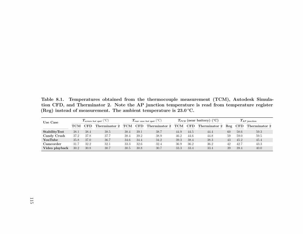
Table 8.1. Temperatures obtained from the thermocouple measurement (TCM), Autodesk Simula-tion CFD, and Therminator 2. Note the AP junction temperature is read from temperature register(Reg) instead of measurement. The ambient temperature is 23.0 ∘C.
Use Case 𝑇screen hot spot (∘C) 𝑇rear case hot spot (∘C) 𝑇PCB (near battery) (∘C) 𝑇AP junction
TCM CFD Therminator 2 TCM CFD Therminator 2 TCM CFD Therminator 2 Reg CFD Therminator 2StabilityTest 38.1 38.4 38.5 38.4 39.1 38.7 44.9 44.5 44.4 60 58.6 59.3Candy Crush 37.2 37.8 37.7 38.4 39.2 38.9 46.2 44.6 44.8 59 59.0 59.5YouTube 35.8 37.0 36.7 34.6 34.4 34.2 39.3 38.4 38.3 43 45.2 45.4Camcorder 31.7 32.2 32.1 33.3 32.6 32.4 36.9 36.2 36.2 42 42.7 43.3Video playback 30.2 30.8 30.7 30.5 30.8 30.7 33.3 33.4 33.4 39 39.4 40.0
115
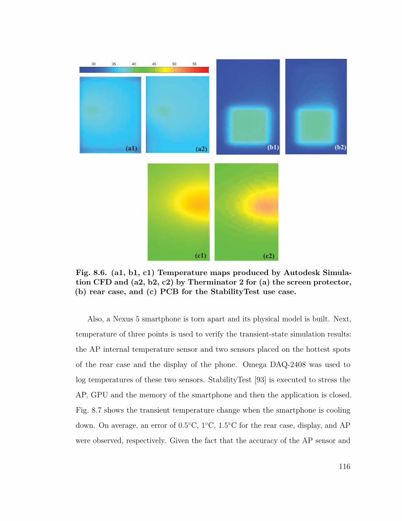
30 35 40 45 50 55
(a1) (a2) (b1) (b2)
(c1) (c2)
Fig. 8.6. (a1, b1, c1) Temperature maps produced by Autodesk Simula-tion CFD and (a2, b2, c2) by Therminator 2 for (a) the screen protector,(b) rear case, and (c) PCB for the StabilityTest use case.
Also, a Nexus 5 smartphone is torn apart and its physical model is built. Next,
temperature of three points is used to verify the transient-state simulation results:
the AP internal temperature sensor and two sensors placed on the hottest spots
of the rear case and the display of the phone. Omega DAQ-2408 was used to
log temperatures of these two sensors. StabilityTest [93] is executed to stress the
AP, GPU and the memory of the smartphone and then the application is closed.
Fig. 8.7 shows the transient temperature change when the smartphone is cooling
down. On average, an error of 0.5∘C, 1∘C, 1.5∘C for the rear case, display, and AP
were observed, respectively. Given the fact that the accuracy of the AP sensor and
116
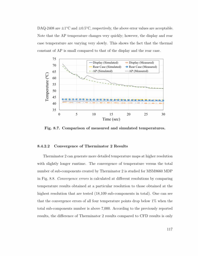
DAQ-2408 are ±1∘C and ±0.5∘C, respectively, the above error values are acceptable.
Note that the AP temperature changes very quickly; however, the display and rear
case temperature are varying very slowly. This shows the fact that the thermal
constant of AP is small compared to that of the display and the rear case.
5 10 15 20 25 30 35
Chart Title
Series1 Series2
35
40
45
50
55
60
65
70
75
0 5 10 15 20 25 30
Tem
pere
ture
(ºC
)
Time (sec)
Display (Simulated) Display (Measured)Rear Case (Simulated) Rear Case (Measured)AP (Simulated) AP (Measured)
Fig. 8.7. Comparison of measured and simulated temperatures.
8.4.2.2 Convergence of Therminator 2 Results
Therminator 2 can generate more detailed temperature maps at higher resolution
with slightly longer runtime. The convergence of temperature versus the total
number of sub-components created by Therminator 2 is studied for MSM8660 MDP
in Fig. 8.8. Convergence errors is calculated at different resolutions by comparing
temperature results obtained at a particular resolution to those obtained at the
highest resolution that are tested (18,109 sub-components in total). One can see
that the convergence errors of all four temperature points drop below 1% when the
total sub-components number is above 7,000. According to the previously reported
results, the difference of Therminator 2 results compared to CFD results is only
117
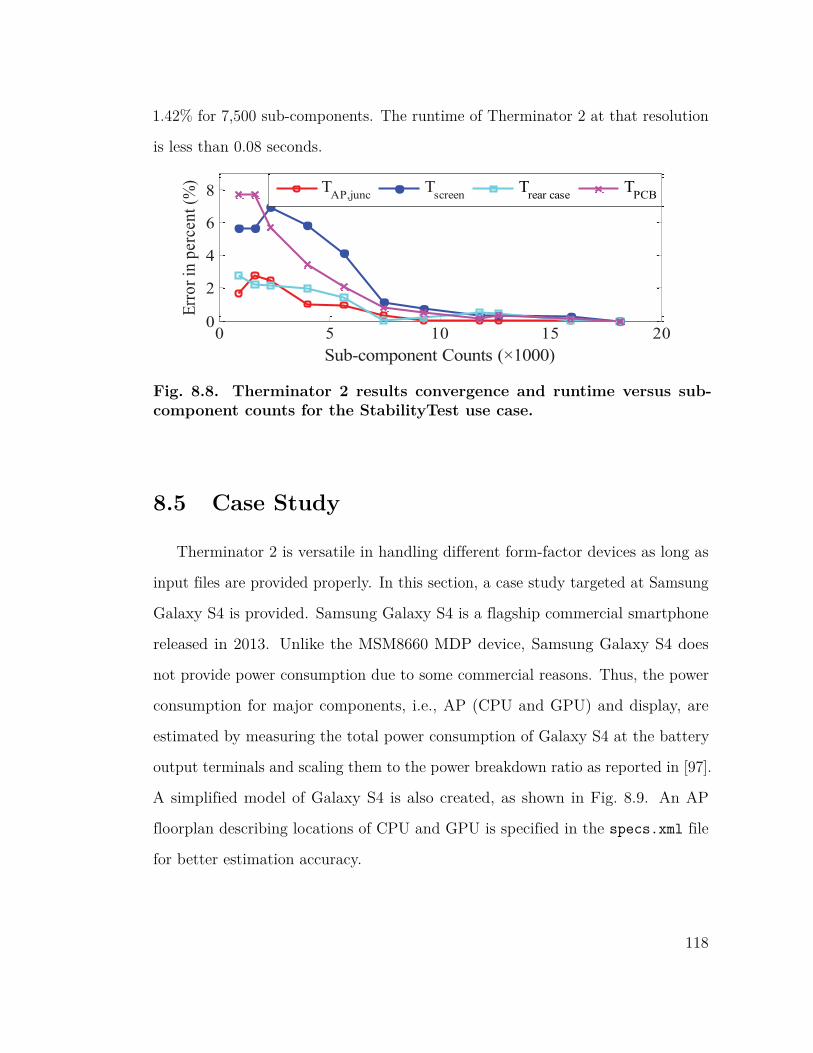
1.42% for 7,500 sub-components. The runtime of Therminator 2 at that resolution
is less than 0.08 seconds.
0 5 10 15 200
2
4
6
8
Sub-component Counts (×1000)
Erro
r in
perc
ent (
%) TAP,junc Tscreen Trear case TPCB
Fig. 8.8. Therminator 2 results convergence and runtime versus sub-component counts for the StabilityTest use case.
8.5 Case Study
Therminator 2 is versatile in handling different form-factor devices as long as
input files are provided properly. In this section, a case study targeted at Samsung
Galaxy S4 is provided. Samsung Galaxy S4 is a flagship commercial smartphone
released in 2013. Unlike the MSM8660 MDP device, Samsung Galaxy S4 does
not provide power consumption due to some commercial reasons. Thus, the power
consumption for major components, i.e., AP (CPU and GPU) and display, are
estimated by measuring the total power consumption of Galaxy S4 at the battery
output terminals and scaling them to the power breakdown ratio as reported in [97].
A simplified model of Galaxy S4 is also created, as shown in Fig. 8.9. An AP
floorplan describing locations of CPU and GPU is specified in the specs.xml file
for better estimation accuracy.
118
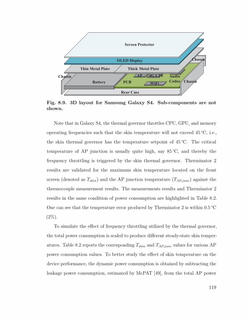
eMMC
PCBBattery ChassisChassis
Rear Case
WiFi
AP 4G LTE Audio Codec
Screen Protector
OLED Display
Thin Metal Plate Thick Metal Plate
Chassis
Fig. 8.9. 3D layout for Samsung Galaxy S4. Sub-components are notshown.
Note that in Galaxy S4, the thermal governor throttles CPU, GPU, and memory
operating frequencies such that the skin temperature will not exceed 45 ∘C, i.e.,
the skin thermal governor has the temperature setpoint of 45 ∘C. The critical
temperature of AP junction is usually quite high, say 85 ∘C, and thereby the
frequency throttling is triggered by the skin thermal governor. Therminator 2
results are validated for the maximum skin temperature located on the front
screen (denoted as 𝑇𝑠𝑘𝑖𝑛) and the AP junction temperature (𝑇𝐴𝑃,𝑗𝑢𝑛𝑐) against the
thermocouple measurement results. The measurements results and Therminator 2
results in the same condition of power consumption are highlighted in Table 8.2.
One can see that the temperature error produced by Therminator 2 is within 0.5 ∘C
(2%).
To simulate the effect of frequency throttling utilized by the thermal governor,
the total power consumption is scaled to produce different steady-state skin temper-
atures. Table 8.2 reports the corresponding 𝑇𝑠𝑘𝑖𝑛 and 𝑇𝐴𝑃,𝑗𝑢𝑛𝑐 values for various AP
power consumption values. To better study the effect of skin temperature on the
device performance, the dynamic power consumption is obtained by subtracting the
leakage power consumption, estimated by McPAT [49], from the total AP power
119
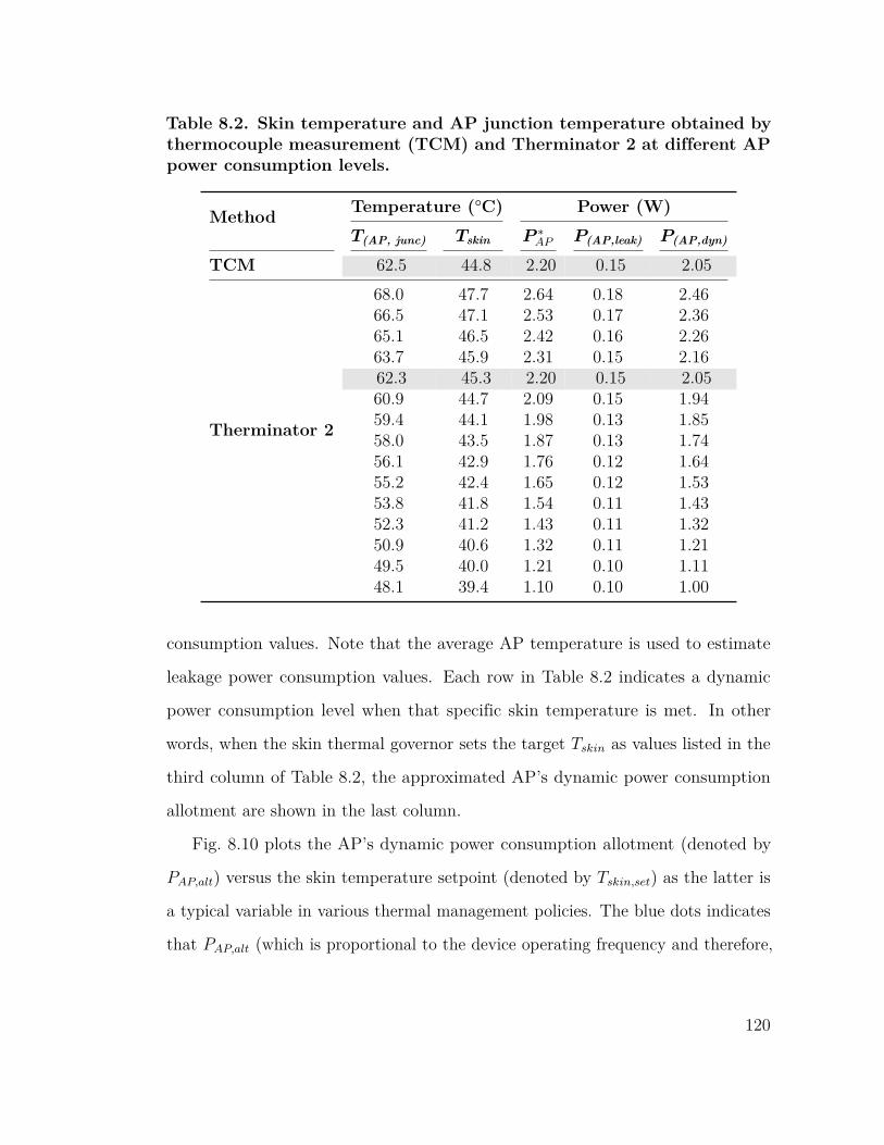
Table 8.2. Skin temperature and AP junction temperature obtained bythermocouple measurement (TCM) and Therminator 2 at different APpower consumption levels.
Method Temperature (∘C) Power (W)𝑇(AP, junc) 𝑇skin 𝑃 *
𝐴𝑃 𝑃(AP,leak) 𝑃(AP,dyn)
TCM 62.5 44.8 2.20 0.15 2.05
Therminator 2
68.0 47.7 2.64 0.18 2.4666.5 47.1 2.53 0.17 2.3665.1 46.5 2.42 0.16 2.2663.7 45.9 2.31 0.15 2.1662.3 45.3 2.20 0.15 2.0560.9 44.7 2.09 0.15 1.9459.4 44.1 1.98 0.13 1.8558.0 43.5 1.87 0.13 1.7456.1 42.9 1.76 0.12 1.6455.2 42.4 1.65 0.12 1.5353.8 41.8 1.54 0.11 1.4352.3 41.2 1.43 0.11 1.3250.9 40.6 1.32 0.11 1.2149.5 40.0 1.21 0.10 1.1148.1 39.4 1.10 0.10 1.00
consumption values. Note that the average AP temperature is used to estimate
leakage power consumption values. Each row in Table 8.2 indicates a dynamic
power consumption level when that specific skin temperature is met. In other
words, when the skin thermal governor sets the target 𝑇𝑠𝑘𝑖𝑛 as values listed in the
third column of Table 8.2, the approximated AP’s dynamic power consumption
allotment are shown in the last column.
Fig. 8.10 plots the AP’s dynamic power consumption allotment (denoted by
𝑃𝐴𝑃,𝑎𝑙𝑡) versus the skin temperature setpoint (denoted by 𝑇𝑠𝑘𝑖𝑛,𝑠𝑒𝑡) as the latter is
a typical variable in various thermal management policies. The blue dots indicates
that 𝑃𝐴𝑃,𝑎𝑙𝑡 (which is proportional to the device operating frequency and therefore,
120
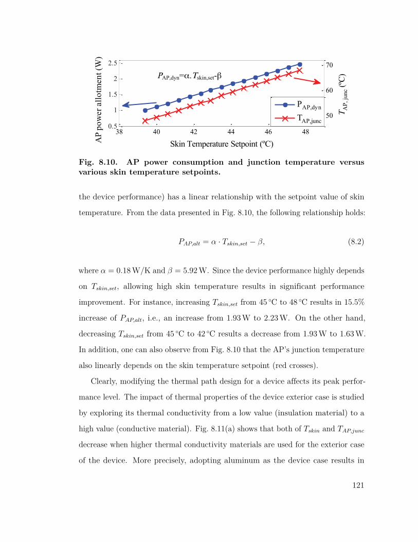
0.5
1
1.5
2
2.5
AP
pow
er a
llotm
ent (
W)
Skin Temperature Setpoint (ºC)
PAP,dyn=α skin,set-β
38 40 42 44 46 48
50
60
70
T AP,
junc
(ºC)
PAP,dyn
TAP,junc
Fig. 8.10. AP power consumption and junction temperature versusvarious skin temperature setpoints.
the device performance) has a linear relationship with the setpoint value of skin
temperature. From the data presented in Fig. 8.10, the following relationship holds:
𝑃𝐴𝑃,𝑎𝑙𝑡 = 𝛼 · 𝑇𝑠𝑘𝑖𝑛,𝑠𝑒𝑡 − 𝛽, (8.2)
where 𝛼 = 0.18 W/K and 𝛽 = 5.92 W. Since the device performance highly depends
on 𝑇𝑠𝑘𝑖𝑛,𝑠𝑒𝑡, allowing high skin temperature results in significant performance
improvement. For instance, increasing 𝑇𝑠𝑘𝑖𝑛,𝑠𝑒𝑡 from 45 ∘C to 48 ∘C results in 15.5%
increase of 𝑃𝐴𝑃,𝑎𝑙𝑡, i.e., an increase from 1.93 W to 2.23 W. On the other hand,
decreasing 𝑇𝑠𝑘𝑖𝑛,𝑠𝑒𝑡 from 45 ∘C to 42 ∘C results a decrease from 1.93 W to 1.63 W.
In addition, one can also observe from Fig. 8.10 that the AP’s junction temperature
also linearly depends on the skin temperature setpoint (red crosses).
Clearly, modifying the thermal path design for a device affects its peak perfor-
mance level. The impact of thermal properties of the device exterior case is studied
by exploring its thermal conductivity from a low value (insulation material) to a
high value (conductive material). Fig. 8.11(a) shows that both of 𝑇𝑠𝑘𝑖𝑛 and 𝑇𝐴𝑃,𝑗𝑢𝑛𝑐
decrease when higher thermal conductivity materials are used for the exterior case
of the device. More precisely, adopting aluminum as the device case results in
121
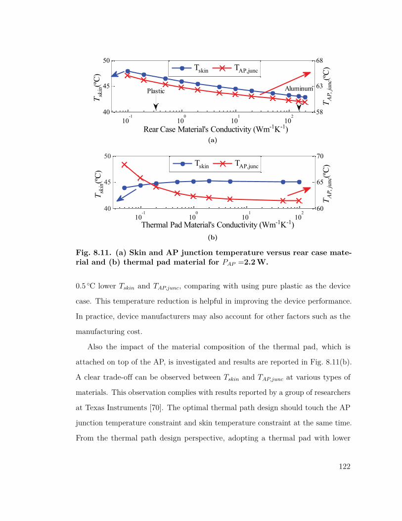
40
45
50
T skin
(ºC)
Rear Case Material's Conductivity (Wm-1K-1)10
-110
010
110
258
63
68
T AP,
junc
(ºC)Tskin TAP,junc
Plastic Aluminum
(a)
40
45
50
T skin
(ºC)
Thermal Pad Material's Conductivity (Wm-1K-1)10
-110
010
110
260
65
70
T AP,
junc
(ºC)Tskin TAP,junc
(b)
Fig. 8.11. (a) Skin and AP junction temperature versus rear case mate-rial and (b) thermal pad material for 𝑃𝐴𝑃 =2.2 W.
0.5 ∘C lower 𝑇𝑠𝑘𝑖𝑛 and 𝑇𝐴𝑃,𝑗𝑢𝑛𝑐, comparing with using pure plastic as the device
case. This temperature reduction is helpful in improving the device performance.
In practice, device manufacturers may also account for other factors such as the
manufacturing cost.
Also the impact of the material composition of the thermal pad, which is
attached on top of the AP, is investigated and results are reported in Fig. 8.11(b).
A clear trade-off can be observed between 𝑇𝑠𝑘𝑖𝑛 and 𝑇𝐴𝑃,𝑗𝑢𝑛𝑐 at various types of
materials. This observation complies with results reported by a group of researchers
at Texas Instruments [70]. The optimal thermal path design should touch the AP
junction temperature constraint and skin temperature constraint at the same time.
From the thermal path design perspective, adopting a thermal pad with lower
122
thermal conductivity on top of the AP achieves better performance. This is because
𝑇𝑠𝑘𝑖𝑛 is usually more critical in smartphones and a low thermal conductivity material
hinders the heat flow to the device skin. However, in practice, some other factors
(such as accelerated aging of the AP and high leakage power at high temperatures)
may prevent the usage of low thermal conductivity materials.
8.6 Summary
This chapter presented Therminator 2, a component-level compact-thermal-
modeling-based thermal simulator targeting small form-factor devices. Thermina-
tor 2 is an early-stage, full-device thermal analyzer that quickly produces accurate
steady- and transient-state temperature maps of all components (ICs, boards,
screens, cases, etc.) in a smartphone, from the application processor to the skin of
the device, with a fast runtime. Therminator 2 provides great flexibility in handling
different user-specified design specifications and use cases. Temperature results
produced by Therminator 2 were validated against real temperature measurements
using thermocouples and simulations using a commercial computational-fluid-
dynamics tool on Qualcomm MSM8660 MDP and Nexus 5. Also a case study on
Samsung Galaxy S4 was provided by using Therminator 2, showing that the device
performance was linearly related to the device skin temperature. In addition, the
impact of the thermal path design on the skin and AP junction temperature was
also studied.
123
9ThermTap: A Power Analyzer and Thermal
Simulator
9.1 Overview
In the past five years, portable devices have become an integral and indispensable
part of our life. In 2011, smartphones and tablets have surpassed the sale of PCs
and become the dominant part of consumer electronics [98]. Main technological
barriers against advancement and further penetration of these devices into our
everyday life include relatively high power consumption and their small form-factor,
which limits the amount of energy storage that can be integrated into these devices.
Moreover, these devices have a very strict thermal envelope. As it is explained
in Chapter 8, mobile device has two types of thermal constraints. The first one
(similar to PCs) is the die temperature constraint. This constraint makes sure
that the application processor (AP) which contains CPU, GPU, and some other
components runs below a certain temperature all the time. The second constraint
is called the skin temperature constraint which is unique to mobile devices [3, 99].
It ensures that the temperature at the surface (or skin) of the device remains low
to avoid any user discomfort or skin burn.
In order to ensure that a device adheres with the aforementioned power and
124
thermal constraints, precise modelings and measurements are required during the
design and prototyping. Due to the very limited resources available on portable
devices, their software should be designed in power- and thermal-aware manners.
One simple solution is to embed temperature sensors as well as current sensors
into every major component of the device in order to measure their temperature
and power consumption. The main drawback of this solution is that in a complex
multithreading and multitasking environment, sensors are blind to which applica-
tions/processes affect the temperature and cause the temperature rise. Furthermore,
sensors do not provide temperature maps for their respective component and thus,
cannot determine workload-dependent hot spots. Besides, deployment of accurate
temperature sensors increases the cost of the device and hence is not desirable.
Moreover, use of external sensors might not be practical and indeed unaffordable
for many software or system developers [100].
In this chapter, I introduce ThermTap, which enables system and software
developers to monitor the power consumption and temperature of various hardware
components in a portable device as a function of running applications and processes.
ThermTap comprises of two important parts: a power analyzer called PowerTap
and an online thermal simulator called Therminator 2.
PowerTap collates the operating state and activity information of various system
components in the device from the operating system (OS) device driver layer. This
is done in an event-driven manner as opposed to a sampling-based method, which
has a high overhead and tends to be slow [76, 77]. I use SystemTap which is
an industry-standard kernel debugging and performance monitoring tool [101].
SystemTap allows dynamically adding probes inside a running kernel without any
destructive side-effect. In this chapter, I use the term probing as a method for
printing (or aggregating) debugging information at specific points in the executable
125
code. SystemTap generates loadable kernel modules and guarantees very low
overhead [102]. For instance, one may place a probe at the entry point of a kernel
function which is responsible for sending data packets over WiFi and another probe
at its return point. Using these two probes, the time it takes to transmit the data
can be determined by calculating the difference between the triggering times of the
first and second probes. Moreover, the second probe reports the amount of data
that is successfully sent through WiFi.
By leveraging the wealth of information that resides in the kernel, PowerTap
adopts properly-tuned accurate power macro-models in order to generate power
traces. Note that obtaining data from the kernel enables PowerTap to determine
per-component power consumption of each application and process (an application
comprises of single or multiple processes).
Subsequently, Therminator 2 (which comprises of transient- and steady-state
thermal solvers) receives the power trace from PowerTap every second and produces
thermal maps at the same rate, a process which I call online thermal analysis.
Given the physical characteristics of the portable device, Therminator 2 builds
a compact thermal model (CTM) of the device, and then generates temperature
maps for every device component, from the device skin to the AP. These maps can
be produced for each application or process, which give important insights about
the device and the software it runs. More specifically, a developer may use this
information to determine applications/processes causing the temperature rise. In
other words, the developer can use ThermTap framework for thermal debugging.
To the best of my knowledge, ThermTap is the first online power analyzer and
thermal simulator for Android devices that enables device manufacturers as well
as developers to debug thermal issues in the system software and applications. I
would like to emphasize the fact that ThermTap only requires a USB connection
126
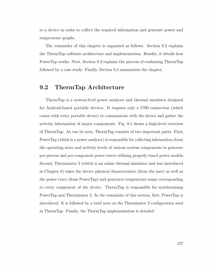
to a device in order to collect the required information and generate power and
temperature graphs.
The remainder of this chapter is organized as follows. Section 9.2 explains
the ThermTap software architecture and implementation. Besides, it details how
PowerTap works. Next, Section 9.3 explains the process of evaluating ThermTap
followed by a case study. Finally, Section 9.4 summarizes the chapter.
9.2 ThermTap Architecture
ThermTap is a system-level power analyzer and thermal simulator designed
for Android-based portable devices. It requires only a USB connection (which
comes with every portable device) to communicate with the device and gather the
activity information of major components. Fig. 9.1 shows a high-level overview
of ThermTap. As can be seen, ThermTap consists of two important parts. First,
PowerTap (which is a power analyzer) is responsible for collecting information about
the operating state and activity levels of various system components to generate
per-process and per-component power traces utilizing properly tuned power models.
Second, Therminator 2 (which is an online thermal simulator and was introduced
in Chapter 8) takes the device physical characteristics (from the user) as well as
the power trace (from PowerTap) and generates temperature maps corresponding
to every component of the device. ThermTap is responsible for synchronizing
PowerTap and Therminator 2. In the remainder of this section, first, PowerTap is
introduced. It is followed by a brief note on the Therminator 2 configuration used
in ThermTap. Finally, the ThermTap implementation is detailed.
127
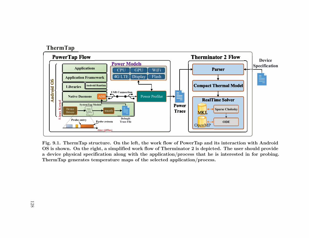
PowerTap Flow
Applications
Application Framework
Libraries Android Runtime
Native Daemons
Lin
ux K
erne
l
USB Connection
PowerTrace
Power ModelsCPU GPU WiFi
4G LTE Display
Probe entry Probe return
time (jiffies)
And
roid
OS
Flash
Therminator 2 Flow
Parser
Compact Thermal Model
RealTime Solver
Sparse Cholesky
ODE
MKL
Applications
Application Framework
Libraries Android Runtime
Native Daemons
Lin
ux K
erne
llL
inux
Ker
nelel
USB Connection
CPU GPU WiFi4G LTE Displayp y
Probe entry Probe return
time (jiffies(( )
Flash
Sparse Cholesky
ODE
ThermTap
OpenMP
Device Specification
Device Drivers tracefs
DebugfsTrace File
SystemTap Module
Power ProfilerADB
Fig. 9.1. ThermTap structure. On the left, the work flow of PowerTap and its interaction with AndroidOS is shown. On the right, a simplified work flow of Therminator 2 is depicted. The user should providea device physical specification along with the application/process that he is interested in for probing.ThermTap generates temperature maps of the selected application/process.
128
9.2.1 PowerTap: A Power Analyzer for Android Devices
PowerTap has two important modules which play key roles to generate power
traces. The first one is a system state monitor, which collects information about the
operating state and activity levels of various system components. The second one is
a power profiler, which utilizes the system state information along with well-tuned
power models for system components to produce power traces.
9.2.1.1 System State Monitor
PowerTap exploits SystemTap [101] for collecting activity profiles. SystemTap
has been developed mainly by Red Hat, IBM, Intel, Hitachi, and Oracle as a tool for
debugging and analyzing the performance of the Linux kernel. It receives an input
script written by the user, which specifies probing codes that must be executed
before and after a set of target instructions (i.e., specific memory locations in the
kernel or user space where probes should be inserted). Next, SystemTap compiles
the script to produce a kernel module, which is subsequently dynamically loaded
into the Linux kernel. Note that since Android is based on Linux, such modules
can be used for Android-based devices as well. When a SystemTap-made kernel
module is loaded, instructions in the specified memory locations are replaced with
breakpoints, which redirect the program execution flow to a user-defined method.
At the end of this method, the removed instruction followed by another user-defined
method and a return instruction are executed. In addition, proper instructions
are inserted before the return instruction to restore the state of previous code
execution flow. This ensures the complete restoration of the CPU state. Fig. 9.2
demonstrates this process. A detailed description on how SystemTap works can be
found in [101].
129
inst
kernel/user codeInstrumented
kernel/user codeInstructions to
be executed before “inst”
Instructions to be executed after “inst”
Collecting informationinst break
point
Fig. 9.2. SystemTap work flow.
In order to calculate the time a certain event takes from start to finish, PowerTap
places probes at the entry and return points of device driver functions. Moreover,
return probes are used to make sure that a certain action is successfully completed.
For instance, one process/application may try to send a packet over WiFi; however,
the packet might be dropped due to weak WiFi coverage. Checking the return
probe allows detection of such situations. Note that PowerTap allows multiple
(different) power models to be active at the same time because it records the start
and end times of events and then aggregates the relevant power models for all
active events.
The information gathered by the kernel module is transferred from the kernel
space to the user space in order to be read by the power profiler (see Fig. 9.1). I
use tracefs to export activity log from the kernel space to the user space. Tracefs is
a low-overhead in-memory file system suitable for this purpose [103]. Note that
logging data directly to the disk would increase the system load significantly and
hence is avoided. Finally, PowerTap connects to the device using Android Debug
Bridge (ADB) through a USB cable, in order to collect the information stored
inside the tracefs buffer.
130
9.2.1.2 Power Profiler
In this chapter, I use a Google Nexus 5 running Android 5.0 as the target
device for training power models. Nexus 5 comes with a quad-core Qualcomm
Snapdragon 800 processor and 2 GB memory. Please note that the power models
presented in this section are general and can be applied to other portable devices.
In order to execute (synthetic as well as standard) benchmarks while control-
ling/monitoring the power state of various system components, I connect the phone
to a PC through a USB cable. The total power consumption of the device (𝑃 𝑡𝑜𝑡𝑎𝑙𝑑𝑒𝑣𝑖𝑐𝑒)
is calculated as
𝑃 𝑡𝑜𝑡𝑎𝑙𝑑𝑒𝑣𝑖𝑐𝑒 = 𝑉𝑈𝑆𝐵𝐼𝑈𝑆𝐵 + 𝑉𝑏𝑎𝑡𝐼𝑏𝑎𝑡, (9.1)
where 𝑉𝑈𝑆𝐵 and 𝑉𝑏𝑎𝑡 denote the voltages provided by the USB and the battery,
respectively, whereas 𝐼𝑈𝑆𝐵 and 𝐼𝑏𝑎𝑡 are currents supplied from the USB and the
battery to the phone, accordingly. 𝐼𝑈𝑆𝐵 is measured by cutting the USB power
lane and placing it in series with an ammeter (NI-9227) to log the current. 𝐼𝑏𝑎𝑡 is
logged similarly. Besides, 𝑉𝑏𝑎𝑡 is measured and logged using a voltmeter (NI-9239).
The sampling rate for both NI-9227 and NI-9239 is set to 2 kHz. Note that based
on the USB 2.0 specification, 𝑉𝑈𝑆𝐵 is fixed at 5 V, whereas 𝐼𝑈𝑆𝐵 can be at most
0.5 A. The second term in Eq. (9.1) is usually negative due to the direction of 𝐼𝑏𝑎𝑡
which shows that the USB current not only supplies the phone but also charges the
battery. However, the smartphone under a heavy load may draw more than 0.5A
current which changes the direction of 𝐼𝑏𝑎𝑡 from negative to positive and forces the
battery to provide current to the system.
Knowing the value of 𝑃 𝑡𝑜𝑡𝑎𝑙𝑑𝑒𝑣𝑖𝑐𝑒, the power consumption of major components is
found as follows. First, all components (except CPU) are turned off, for instance,
131
GPU, WiFi, 4G, and display. Note that because CPU is always on during bench-
marking, it is characterized first. Also, all background processes are stopped (this
is a feature provided by Android). As a result, the power consumption of each
component can be characterized individually by selectively turning it on. Next,
CPU power model is characterized using the StabilityTest benchmark [93]. After
that, each major component is turned on using synthetic benchmarks and the
total power of the smartphone is measured. Knowing the CPU power model, the
CPU power consumption is calculated and subtracted from the measured 𝑃 𝑡𝑜𝑡𝑎𝑙𝑑𝑒𝑣𝑖𝑐𝑒
to determine the power consumption of the component of interest. The power of
the remainder of system (which belongs to components that are not considered)
is captured as a constant and assigned to the main PCB of the device. In the
remainder of this subsection, the power models that I have derived are briefly
explained.
CPU power modeling: Initially, I disable all CPU cores except one. Next,
a power model for a single core is derived. Then, cores are activated one by one
and their power consumptions in a fully utilized state are measured for different
frequencies. I observed that the power consumption of each core changes based on
the total number of active cores. Fig. 9.3 depicts the power consumption of a single
active core with respect to the total number of active cores drawn at six different
clock frequencies. For these measurements, all of the cores are fully utilized and
Android power and thermal governors are turned off. As can be seen in Fig. 9.3, at
higher frequencies, the dependence of individual core power consumption on the
total number of active cores becomes more pronounced. Moreover, as I explain
below, the per-core power consumption is minimum when the number of active
cores in the target system is two.
Before presenting the detailed CPU power consumption model, I define some
132
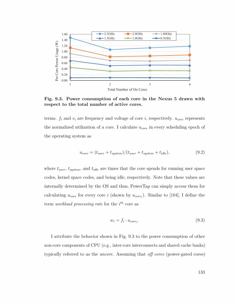
Fig. 9.3. Power consumption of each core in the Nexus 5 drawn withrespect to the total number of active cores.
terms. 𝑓𝑖 and 𝑣𝑖 are frequency and voltage of core 𝑖, respectively. 𝑢𝑐𝑜𝑟𝑒 represents
the normalized utilization of a core. I calculate 𝑢𝑐𝑜𝑟𝑒 in every scheduling epoch of
the operating system as
𝑢𝑐𝑜𝑟𝑒 = (𝑡𝑢𝑠𝑒𝑟 + 𝑡𝑠𝑦𝑠𝑡𝑒𝑚)/(𝑡𝑢𝑠𝑒𝑟 + 𝑡𝑠𝑦𝑠𝑡𝑒𝑚 + 𝑡𝑖𝑑𝑙𝑒), (9.2)
where 𝑡𝑢𝑠𝑒𝑟, 𝑡𝑠𝑦𝑠𝑡𝑒𝑚, and 𝑡𝑖𝑑𝑙𝑒 are times that the core spends for running user space
codes, kernel space codes, and being idle, respectively. Note that these values are
internally determined by the OS and thus, PowerTap can simply access them for
calculating 𝑢𝑐𝑜𝑟𝑒 for every core 𝑖 (shown by 𝑢𝑐𝑜𝑟𝑒𝑖). Similar to [104], I define the
term workload processing rate for the 𝑖th core as
𝑤𝑖 = 𝑓𝑖 · 𝑢𝑐𝑜𝑟𝑒𝑖. (9.3)
I attribute the behavior shown in Fig. 9.3 to the power consumption of other
non-core components of CPU (e.g., inter-core interconnects and shared cache banks)
typically referred to as the uncore. Assuming that off cores (power-gated cores)
133
consume zero power and considering that on cores consume dynamic plus active
leakage power during program execution but only standby leakage power when
sitting idle, the total CPU power consumption (𝑃𝐶𝑃 𝑈) can be modeled as
𝑃𝐶𝑃 𝑈 = (𝑃 𝑑𝑦𝑛𝑐𝑜𝑟𝑒𝑠 + 𝑃 𝑙𝑒𝑎𝑘
𝑐𝑜𝑟𝑒𝑠) + 𝑃𝑢𝑛𝑐𝑜𝑟𝑒
=∑︁
𝑖∈{on cores}
(︁𝛽𝑑𝑦𝑛
𝑐𝑜𝑟𝑒(𝑣𝑖) · 𝑓𝑖 · 𝑢𝑐𝑜𝑟𝑒𝑖+ 𝛽𝑙𝑒𝑎𝑘
𝑐𝑜𝑟𝑒(𝑣𝑖))︁
+ 𝛽𝑢𝑛𝑐𝑜𝑟𝑒(𝑤𝑡𝑜𝑡, 𝑛𝑜𝑛), (9.4)
where 𝛽𝑑𝑦𝑛𝑐𝑜𝑟𝑒(𝑣𝑖), 𝛽𝑙𝑒𝑎𝑘
𝑐𝑜𝑟𝑒(𝑣𝑖), and 𝛽𝑢𝑛𝑐𝑜𝑟𝑒(𝑤𝑡𝑜𝑡, 𝑛𝑜𝑛) are lookup table-based fitting func-
tions; 𝑤𝑡𝑜𝑡 is the total workload processing rate of CPU which is defined as
𝑤𝑡𝑜𝑡 =∑︁
𝑖∈{on cores}𝑤𝑖. (9.5)
I expect 𝛽𝑑𝑦𝑛𝑐𝑜𝑟𝑒(𝑣𝑖) to be a quadratic function of 𝑣𝑖, whereas 𝛽𝑙𝑒𝑎𝑘
𝑐𝑜𝑟𝑒(𝑣𝑖) to be a linear
function of 𝑣𝑖. In addition, 𝛽𝑢𝑛𝑐𝑜𝑟𝑒(𝑤𝑡𝑜𝑡, 𝑛𝑜𝑛) should be a linearly increasing function
of 𝑤𝑡𝑜𝑡 and a convex function of 𝑛𝑜𝑛, where the minimum is achieved for a certain
number of on cores, called 𝑛𝑜𝑝𝑡𝑜𝑛 . As mentioned before, 𝑛𝑜𝑝𝑡
𝑜𝑛 in Fig. 9.3 is equal to
2. Note that the non-proportionality of energy of CPUs [105] arises in part due to
core leakage and uncore power consumption terms.
GPU power modeling: Nexus 5 has an Adreno 330 integrated into the
AP for 2D and 3D graphic processing. Adreno 330 shares main memory with
the processor [106]. Hence, I only need to account for the power consumption
of the GPU core. Android uses a driver called Kernel Graphics Support Layer
(KGSL) developed by Qualcomm to provide a Hardware Abstraction Layer (HAL)
for userspace Adreno drivers. KGSL allows various processes to create different
GPU contexts, which are analogous to CPU processes. At each point in time,
only a single context can be executed on GPU. KGSL is responsible to perform
134
context switching. Finally, a context is destroyed when its execution is finished
or an exception is occurred. By tracing context create requests, one can simply
determine which context belongs to which process, and consequently, assign the
related GPU power consumption to the right process. Adreno 330 supports DVFS
through a proprietary closed-source policy called trustzone. KGSL is responsible of
applying actions determined by the policy to the GPU hardware.
Based on the above discussion, I model the GPU power consumption as
𝑃𝐺𝑃 𝑈 = 𝛽𝑑𝑦𝑛𝐺𝑃 𝑈(𝑣) · 𝑓 · 𝑢𝐺𝑃 𝑈 + 𝛽𝑙𝑒𝑎𝑘
𝐺𝑃 𝑈(𝑣), (9.6)
where 𝛽𝑑𝑦𝑛𝐺𝑃 𝑈 (𝑣) and 𝛽𝑙𝑒𝑎𝑘
𝐺𝑃 𝑈 (𝑣) are lookup-based fitting functions of the GPU voltage
level (denoted by 𝑣), 𝑓 is the GPU frequency, and 𝑢𝐺𝑃 𝑈 represents the normalized
utilization of GPU.
WiFi & 4G-LTE power modeling: I measured the WiFi power consump-
tion during send and receive operations. It has been observed that the power
consumption of WiFi while receiving data is linearly proportional to the receive
rate, whereas during the send operation, it behaves as a piecewise linear function
with two thresholds; one occurs at 2 Mbps, and the other one happens at 8 Mbps.
Similar behavior was observed for 4G-LTE with different thresholds.
Display power modeling: Nexus 5 has a full-HD IPS LCD display. As
a result, the display power is linearly proportional to its brightness. This is in
contrast to OLED displays, where the screen content plays a major role in the
power consumption [76,77]. Thus the display power can be modeled as
𝑃𝐷𝑖𝑠𝑝𝑙𝑎𝑦 = 𝛽𝐷𝑖𝑠𝑝𝑙𝑎𝑦 ·𝐵𝑟𝑖𝑔ℎ𝑡𝑛𝑒𝑠𝑠, (9.7)
where 𝛽𝐷𝑖𝑠𝑝𝑙𝑎𝑦 is the linearization coefficient and 𝐵𝑟𝑖𝑔ℎ𝑡𝑛𝑒𝑠𝑠 is the normalized
135
brightness value which varies from 0 to 1. According to my measurements, the IPS
LCD display consumes nearly zero power when it is completely dim.
Flash storage power modeling: It is observed that when the data transfer
rate (write or read) is low, the flash consumes significantly less power. I conjecture
that in low transfer rates, caching and write back methods are used (as opposed to
the write through technique). On the other hand, in high transfer rates, the power
consumption becomes significant. Hence, I define a threshold for the transfer rate
called 𝛽𝑡ℎ𝑟𝑒𝑓𝑙𝑎𝑠ℎ and model the flash power consumption (separately for read and write
operations) as
𝑃𝑓𝑙𝑎𝑠ℎ =
⎧⎪⎪⎪⎨⎪⎪⎪⎩𝛽𝑠𝑙𝑜𝑤
𝑓𝑙𝑎𝑠ℎ, if transfer rate < 𝛽𝑡ℎ𝑟𝑒𝑓𝑙𝑎𝑠ℎ
𝛽𝑓𝑎𝑠𝑡𝑓𝑙𝑎𝑠ℎ, otherwise.
, (9.8)
where 𝛽𝑠𝑙𝑜𝑤𝑓𝑙𝑎𝑠ℎ and 𝛽𝑓𝑎𝑠𝑡
𝑓𝑙𝑎𝑠ℎ denote the power consumption of the flash in low and
high transfer rates, respectively. 𝛽𝑡ℎ𝑟𝑒𝑓𝑙𝑎𝑠ℎ for the read and write operation is about
70 MB/s.
9.2.2 Therminator 2: An Online Thermal Simulator
The Therminator 2 runtime for the steady-state analysis is measured to be
below 0.35 seconds even for systems with very large subcomponent count (∼18,000).
This delay is not noticeable by the ThermTap user because the steady-state solver
is required to be called once to derive the initial temperature used for the transient-
state analysis. For the transient-state analysis, Therminator 2 can calculate the
device temperature after one second in real time (in less than one wall-clock second)
when the number of subcomponents in the system is nearly 5,000. Thus, I perform
all of measurements with this maximum component count.
136
9.2.3 ThermTap Implementation
PowerTap is implemented in Java, whereas Therminator 2 is implemented
in C++ (as explained in Chapter 8). ThermTap, which is also written in Java,
synchronizes PowerTap and Therminator 2 through the file system. I tested
ThermTap on a Linux machine (Debian 8) with a quad-core Intel Core i7-3770
processor running at 3.4GHz and 8GB of memory.
9.3 ThermTap Evaluation
I first calibrated PowerTap to make sure accurate power traces are generated.
Different benchmarks are executed to train power models. I measured the CPU
runtime overhead of inserting the SystemTap module as 1.7% under heavy load
which is very low as expected. Fig. 9.4 demonstrates a test case which shows
how Android thermal manager works. Initially, the system was in the idle state.
Next, StabilityTest benchmark was executed. This benchmark heavily stresses
CPU and memory. After 40 seconds, the total power consumption drops due to
the overheating issue which causes the thermal manager to throttle frequencies of
CPU cores. This figure also shows that how well PowerTap estimations follow the
measurement values. On average, power estimations of PowerTap differed from
measured values by 15%.
Next, I used power values generated by PowerTap to calibrate ThermTap.
Similar to the technique described in Chapter 8, I tore apart a Nexus 5 smartphone
to build its physical model. I used temperatures of three points to calibrate and
verify ThermTap results: the AP internal temperature sensor and two sensors
placed on the hottest spots of the rear case and the display of the phone. Omega
DAQ-2408 was used to log temperatures of these two sensors. Fig. 8.7 in Chapter 8
137
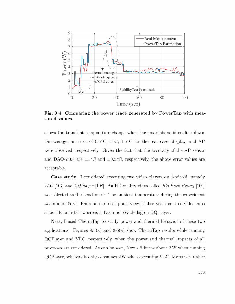
Thermal manager throttles frequency
of CPU cores
StabilityTest benchmarkIdle
Fig. 9.4. Comparing the power trace generated by PowerTap with mea-sured values.
shows the transient temperature change when the smartphone is cooling down.
On average, an error of 0.5 ∘C, 1 ∘C, 1.5 ∘C for the rear case, display, and AP
were observed, respectively. Given the fact that the accuracy of the AP sensor
and DAQ-2408 are ±1 ∘C and ±0.5 ∘C, respectively, the above error values are
acceptable.
Case study: I considered executing two video players on Android, namely
VLC [107] and QQPlayer [108]. An HD-quality video called Big Buck Bunny [109]
was selected as the benchmark. The ambient temperature during the experiment
was about 25 ∘C. From an end-user point view, I observed that this video runs
smoothly on VLC, whereas it has a noticeable lag on QQPlayer.
Next, I used ThermTap to study power and thermal behavior of these two
applications. Figures 9.5(a) and 9.6(a) show ThermTap results while running
QQPlayer and VLC, respectively, when the power and thermal impacts of all
processes are considered. As can be seen, Nexus 5 burns about 3 W when running
QQPlayer, whereas it only consumes 2 W when executing VLC. Moreover, unlike
138
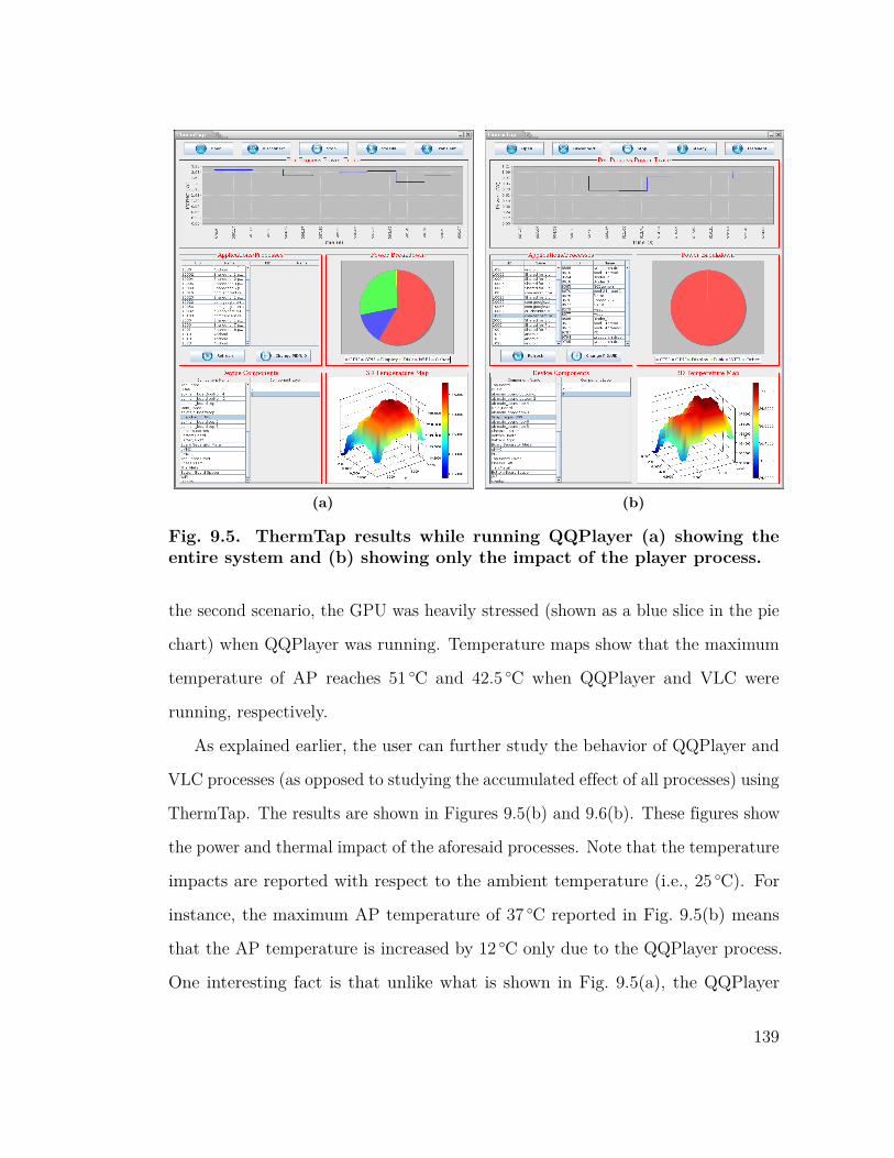
(a) (b)
Fig. 9.5. ThermTap results while running QQPlayer (a) showing theentire system and (b) showing only the impact of the player process.
the second scenario, the GPU was heavily stressed (shown as a blue slice in the pie
chart) when QQPlayer was running. Temperature maps show that the maximum
temperature of AP reaches 51 ∘C and 42.5 ∘C when QQPlayer and VLC were
running, respectively.
As explained earlier, the user can further study the behavior of QQPlayer and
VLC processes (as opposed to studying the accumulated effect of all processes) using
ThermTap. The results are shown in Figures 9.5(b) and 9.6(b). These figures show
the power and thermal impact of the aforesaid processes. Note that the temperature
impacts are reported with respect to the ambient temperature (i.e., 25 ∘C). For
instance, the maximum AP temperature of 37 ∘C reported in Fig. 9.5(b) means
that the AP temperature is increased by 12 ∘C only due to the QQPlayer process.
One interesting fact is that unlike what is shown in Fig. 9.5(a), the QQPlayer
139
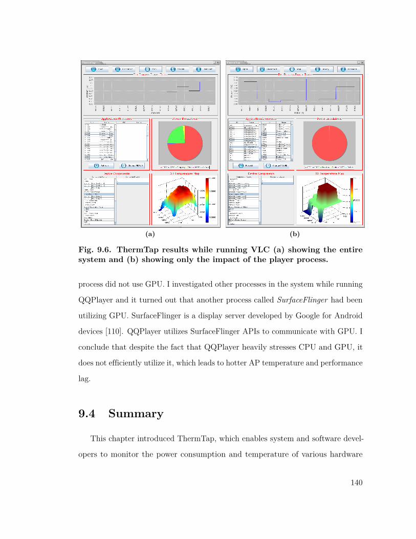
(a) (b)
Fig. 9.6. ThermTap results while running VLC (a) showing the entiresystem and (b) showing only the impact of the player process.
process did not use GPU. I investigated other processes in the system while running
QQPlayer and it turned out that another process called SurfaceFlinger had been
utilizing GPU. SurfaceFlinger is a display server developed by Google for Android
devices [110]. QQPlayer utilizes SurfaceFlinger APIs to communicate with GPU. I
conclude that despite the fact that QQPlayer heavily stresses CPU and GPU, it
does not efficiently utilize it, which leads to hotter AP temperature and performance
lag.
9.4 Summary
This chapter introduced ThermTap, which enables system and software devel-
opers to monitor the power consumption and temperature of various hardware
140
components in a portable device as a function of running applications and processes.
ThermTap is comprised of a power analyzer, called PowerTap, and an online ther-
mal simulator, called Therminator 2. PowerTap generates power traces, whereas
Therminator 2 produces various temperature maps including those for the device
components and device skin. Experimental results confirmed that with the aim
of PowerTap and Therminator 2, ThermTap can generate accurate temperature
maps. Besides this, developers can use ThermTap to find thermal bugs in a system
or application.
141
10Conclusion
In the first part of this dissertation, I identified and addressed three key issues
which facilitate the utilization of TECs inside a server-class CPU cooling package
in a power-efficient manner. To evaluate my proposed solutions, I developed a TEC
simulator called Teculator which enabled me to perform thermal simulations and
validate models and formulations. In all of these solutions, I carefully considered
the strong dependence of leakage power on the temperature. This is the key
difference for employing TECs for cooling electronics devices compared to other
cooling applications where TECs might be adopted.
First, I reformulated the TEC coefficient of performance (COP) to account
for the leakage power because the traditional definition of COP is not useful for
electronic cooling packages due to strong dependence of the circuit leakage power
on the die temperature. Based on this new formulation, I proposed a new compact
thermal model for TECs which considers the leakage power. This model was used
to maximize the new COP metric.
Second, I found the near-optimal TEC driving current and fan rotation speed
in order to either minimize the maximum die temperature or cooling power subject
to thermal constraints. The temperature minimization problem is crucial when
negative effects of the high die temperature is more important compared to the
142
power consumption of the cooling system. On the other hand, the cooling power
minimization problem is critical in power-aware applications. In these optimization
problems, the strong dependence of the leakage power on the temperature was
also considered. Investing more power in the cooling pays off well as a result of a
dramatic power saving in the chip leakage power consumption. Next, I developed a
fast optimization framework called OFTEC in order to find a high-quality solution
to above optimization problems and evaluate the effectiveness of a hybrid cooling
assembly comprised of TECs and a fan. OFTEC uses active-set sequential quadratic
programming (SQP) method for solving these optimization problems.
I expect that implementing the active-set SQP method in C language will
substantially speed-up the runtime which allows OFTEC to be used as an online
controlling algorithm. Also, with the current runtime of OFTEC, one can classify
various die temperatures into different categories and pre-calculate optimization
solutions and store them in a look-up table. In this way, the desired controlling
values can be accessed immediately. Moreover, TECs can improve the heat removal
capacity of steady state cooling solutions for a short period of time (i.e., in the
order of a second). This phenomenon can be used before results of OFTEC become
ready. Results of Chapter 3 suggests to increase the optimum TEC current by
about 1 A for 1 s to reap the benefit of transient cooling.
Third, I suggested that adjacent hot spots with the same thermal behavior can
be grouped and controlled independently by a cluster of TECs because the spatial
and temporal distribution of hot spots on the surface of a chip are non-uniform. A
bypass switch for each TEC cluster was added in order to allow selectively turning
off some TEC clusters which are not needed. More precisely, a clustering problem
was formulated and solved to minimize the power waste due to the excessive use of
TECs.
143
In the second part of this dissertation, I introduced ThermTap, which enables
system and software developers to monitor the power consumption and temperature
of various hardware components in an Android device as a function of running
applications and processes. ThermTap comprises of a power analyzer, called
PowerTap, and an online thermal simulator, called Therminator 2. With accurate
power macro-models, PowerTap collects activity profiles of major components of a
portable device from the operating system kernel device drivers in an event-driven
manner to generate power traces. In turn, Therminator 2 reads these traces and,
using a compact thermal model of the device, generates various temperature maps
including those for the device components and device skin. Fast thermal simulation
techniques enable Therminator 2 to be executed in realtime. With accurate per-
process and per-application temperature maps that ThermTap produces, it enables
software and system developers to find thermal bugs in their software. A case study
was presented on identifying a thermal bug in a software running on an Android
device.
Power models of PowerTap may be extended such that ThermTap can be used
for probing and finding thermal bugs in a wider range of hardware components.
Memory is one of the major power consumers that is not modeled explicitly in this
work. Currently, the cache power consumption is captured in the CPU power and
the DRAM power is distributed between CPU and GPU power values. Another
considerable power consumer is the battery. GPS is also a substantial power
consumer in smartphones, which has a significant impact on the temperature of
the device. Finally, there are other components that contribute to the total power
consumption like power management IC(s) and PCB tracks and pads. These
components can be taken into account in future extensions of ThermTap.
144
Bibliography
[1] W. Huang, K. Rajamani, M. Stan, and K. Skadron, “Scaling with designconstraints: Predicting the future of big chips,” IEEE Micro, vol. 31, pp.16–29, 2011.
[2] M. Pedram and S. Nazarian, “Thermal modeling, analysis, and managementin vlsi circuits: Principles and methods,” Proceedings of the IEEE, vol. 94,no. 8, pp. 1487–1501, 2006.
[3] S. Thomas and Z. Rui, “Thermal management in user space,” in Proceedingsof the Linux Symposium, Jul. 2008, pp. 227–233.
[4] D. Brooks and M. Martonosi, “Dynamic thermal management for high-performance microprocessors,” in Proceedings of the International Symposiumon High-Performance Computer Architecture, Jan. 2001, pp. 171–182.
[5] S. Murali, A. Mutapcic, D. Atienza, R. Gupta, S. Boyd, and G. De Micheli,“Temperature-aware processor frequency assignment for MPSoCs using con-vex optimization,” in Proceedings of the International Conference on Hard-ware/Software Codesign and System Synthesis, Sep. 2007, pp. 111–116.
[6] S. Murali, A. Mutapcic, D. Atienza, R. Gupta, S. Boyd, L. Benini, andG. De Micheli, “Temperature control of high-performance multi-core platformsusing convex optimization,” in Proceedings of the Design, Automation, andTest in Europe, Mar. 2008, pp. 110–115.
[7] A. K. Coskun, T. S. Rosing, and K. C. Gross, “Proactive temperaturemanagement in mpsocs,” in Proceedings of the International Symposium onLow Power Electronics and Design, Aug. 2008, pp. 165–170.
145
[8] A. Kumar, L. Shang, L.-S. Peh, and N. K. Jha, “System-level dynamic thermalmanagement for high-performance microprocessors,” IEEE Transactions onComputer-Aided Design of Integrated Circuits and Systems, vol. 27, no. 1, pp.96–108, 2008.
[9] A. Bartolini, M. Cacciari, A. Tilli, and L. Benini, “Thermal and energymanagement of high-performance multicores: Distributed and self-calibratingmodel-predictive controller,” IEEE Transactions on Parallel and DistributedSystems, vol. 24, no. 1, pp. 170–183, 2013.
[10] Y. Liu, H. Yang, R. P. Dick, H. Wang, and L. Shang, “Thermal vs energyoptimization for dvfs-enabled processors in embedded systems,” in Proceedingsof the International Symposium on Quality Electronic Design, Mar. 2007, pp.204–209.
[11] A. K. Coskun, J. L. Ayala, D. Atienza, T. S. Rosing, and Y. Leblebici,“Dynamic thermal management in 3d multicore architectures,” in Proceedingsof the Design, Automation, and Test in Europe, Apr. 2009, pp. 1410–1415.
[12] A. Bar-Cohen and P. Wang, “On-chip thermal management and hot-spotremediation,” in Nano-Bio- Electronic, Photonic and MEMS Packaging.Springer, 2010, pp. 349–429.
[13] I. Chowdhury, R. Prasher, K. Lofgreen, G. Chrysler, S. Narasimhan, R. Maha-jan, D. Koester, R. Alley, and R. Venkatasubramanian, “On-chip cooling bysuperlattice-based thin-film thermoelectrics,” Nature Nanotechnology, vol. 4,no. 4, pp. 235–238, 2009.
[14] Tellurex Corporation, “Introduction to thermoelectrics,” http://web.archive.org/web/20120907073241/http://www.tellurex.com/pdf/introduction-to-thermoelectrics.pdf, 2010, [Online; accessed 7-16-2015].
[15] M. J. Dousti and M. Pedram, “Platform-dependent, leakage-aware controlof the driving current of embedded thermoelectric coolers,” in Proceedingsof the International Symposium on Low Power Electronics and Design, Sep.2013, pp. 311–316.
[16] ——, “Power-aware deployment and control of forced-convection and thermo-electric coolers,” in Proceedings of the Design Automation Conference, Jun.2014, pp. 1–6.
[17] ——, “Power-efficient control of thermoelectric coolers considering distributedhot spots,” in Proceedings of the Design, Automation, and Test in Europe,Mar. 2015, pp. 966–971.
146
[18] M. J. Dousti, A. Petraglia, and M. Pedram, “Accurate electrothermal modelingof thermoelectric generators,” in Proceedings of the Design, Automation, andTest in Europe, Mar. 2015, pp. 1603–1606.
[19] Q. Xie, M. J. Dousti, and M. Pedram, “Therminator: A thermal simulatorfor smartphones producing accurate chip and skin temperature maps,” inProceedings of the International Symposium on Low Power Electronics andDesign, Aug. 2014, pp. 117–122.
[20] M. J. Dousti, M. Ghasemi-Gol, M. Nazemi, and M. Pedram, “ThermTap:An online power and thermal analyzer for portable devices,” in Proceedingsof the International Symposium on Low Power Electronics and Design, Jul.2015.
[21] D. M. Rowe, Ed., Thermoelectrics handbook: Macro to nano, 1st ed. CRCPress, Dec. 2005.
[22] G. J. Snyder, “Small thermoelectric generators,” Electrochemical SocietyInterface, vol. 17, no. 3, pp. 55–57, 2008.
[23] Y. Ramadass and A. Chandrakasan, “A battery-less thermoelectric energyharvesting interface circuit with 35 mv startup voltage,” IEEE Journal ofSolid-State Circuits, vol. 46, no. 1, pp. 333–341, Jan 2011.
[24] S. Lineykin and S. Ben-Yaakov, “Analysis of thermoelectric coolers by aspice-compatible equivalent-circuit model,” IEEE Power Electronics Letters,vol. 3, no. 2, pp. 63–66, 2005.
[25] P. Y. Hou, R. Baskaran, and K. F. Böhringer, “Optimization of microscalethermoelectric cooling (TEC) element dimensions for hotspot cooling appli-cations,” Journal of Electronic Materials, vol. 38, no. 7, pp. 950–953, Jul.2009.
[26] S. Biswas, M. Tiwari, T. Sherwood, L. Theogarajan, and F. T. Chong, “Fight-ing fire with fire: modeling the datacenter-scale effects of targeted superlatticethermal management,” in Proceedings of the International Symposium onComputer Architecture, Jun. 2011, pp. 331–340.
[27] J. Bierschenk and D. Johnson, “Extending the limits of air cooling withthermoelectrically enhanced heat sinks,” in Proceedings of the IntersocietyConference on Thermal and Thermomechanical Phenomena in ElectronicSystems, Jun. 2004, pp. 679–684.
[28] B. Alexandrov, O. Sullivan, S. Kumar, and S. Mukhopadhyay, “Prospectsof active cooling with integrated super-lattice based thin-film thermoelectric
147
devices for mitigating hotspot challenges in microprocessors,” in Proceedingsof the Asia and South Pacific Design Automation Conference, Jan 2012, pp.633–638.
[29] J. Long, S. O. Memik, and M. Grayson, “Optimization of an on-chip activecooling system based on thin-film thermoelectric coolers,” in Proceedings ofthe Design, Automation, and Test in Europe, Mar. 2010, pp. 117–122.
[30] J. Long and S. Memik, “A framework for optimizing thermoelectric activecooling systems,” in Proceedings of the Design Automation Conference, Jun.2010, pp. 591–596.
[31] D. Shin, S. W. Chung, E.-Y. Chung, and N. Chang, “Energy-optimal dynamicthermal management: Computation and cooling power co-optimization,”IEEE Transactions on Industrial Informatics, vol. 6, pp. 340–351, 2010.
[32] F. Paterna and S. Reda, “Mitigating dark-silicon problems using superlattice-based thermoelectric coolers,” in Proceedings of the Design, Automation, andTest in Europe, Mar. 2013, pp. 1391–1394.
[33] S. Rho, K. Kang, and C.-M. Kyung, “Energy minimization of 3D cache-stacked processor based on thin-film thermoelectric coolers,” in Proceedingsof the International Midwest Symposium on Circuits and Systems, Aug. 2011,pp. 1–4.
[34] S. Beeby and N. White, Eds., Energy harvesting for autonomous systems,1st ed. Artech House, 2010.
[35] J. A. Federici, D. G. Norton, T. Brüggemann, K. Voit, E. Wetzel, and D. Vla-chos, “Catalytic microcombustors with integrated thermoelectric elementsfor portable power production,” Journal of Power Sources, vol. 161, no. 2,pp. 1469–1478, 2006.
[36] C. Lu, S. P. Park, V. Raghunathan, and K. Roy, “Analysis and design ofultra low power thermoelectric energy harvesting systems,” in Proceedingsof the International Symposium on Low Power Electronics and Design, Aug2010, pp. 183–188.
[37] T. Esram and P. L. Chapman, “Comparison of photovoltaic array maximumpower point tracking techniques,” IEEE Transactions on Energy Conversion,vol. 22, no. 2, p. 439, 2007.
[38] J. Sharp, J. Bierschenk, and H. Lyon, “Overview of solid-state thermoelec-tric refrigerators and possible applications to on-chip thermal management,”Proceedings of the IEEE, vol. 94, pp. 1602 –1612, Aug. 2006.
148
[39] R. Yang, G. Chen, A. Ravi Kumar, G. J. Snyder, and J.-P. Fleurial, “Transientcooling of thermoelectric coolers and its applications for microdevices,” EnergyConversion and Management, vol. 46, pp. 1407–1421, Jun. 2005.
[40] K. Skadron, M. R. Stan, W. Huang, S. Velusamy, K. Sankaranarayanan,and D. Tarjan, “Temperature-aware microarchitecture,” ACM SIGARCHComputer Architecture News, vol. 31, no. 2, pp. 2–13, 2003.
[41] K. Wang, R. Baskaran, and K. Bohringer, “Template based high packingdensity assembly for microchip solid state cooling application,” in Proceedingsof the Conference on Foundations of Nanoscience: Selfassembled Architecturesand Devices, Apr. 2006.
[42] M. Gupta, M.-h. Sayer, S. Mukhopadhyay, and S. Kumar, “On-chip peltiercooling using current pulse,” in Proceedings of the Intersociety Conferenceon Thermal and Thermomechanical Phenomena in Electronic Systems, Jun.2010, pp. 1–7.
[43] S. Li, J. H. Ahn, R. D. Strong, J. B. Brockman, D. M. Tullsen, and N. P.Jouppi, “The McPAT framework for multicore and manycore architectures:Simultaneously modeling power, area, and timing,” ACM Transactions onArchitecture and Code Optimization, vol. 10, pp. 5:1–5:29, Apr. 2013.
[44] Y. Liu, R. Dick, L. Shang, and H. Yang, “Accurate temperature-dependentintegrated circuit leakage power estimation is easy,” in Proceedings of theDesign, Automation, and Test in Europe, Apr. 2007, pp. 1526–1531.
[45] I. Sato, K. Otani, M. Mizukami, S. Oguchi, K. Hoshiya, and K.-I. Shimokura,“Characteristics of heat transfer in small disk enclosures at high rotationspeeds,” IEEE Transactions on Components, Hybrids, and ManufacturingTechnology, vol. 13, pp. 1006–1011, 1990.
[46] J. Nocedal and S. J. Wright, Numerical optimization, 2nd ed. Springer,2006.
[47] L. He and W. Liao, “PTscalar v1.0,” http://eda.ee.ucla.edu/PTscalar, Dec.2003, [Online; accessed 7-16-2015].
[48] M. Guthaus, J. Ringenberg, D. Ernst, T. Austin, T. Mudge, and R. Brown,“MiBench: a free, commercially representative embedded benchmark suite,”in Proceedings of the International Workshop on Workload Characterization,Dec. 2001, pp. 3–14.
[49] S. Li, J. H. Ahn, R. D. Strong, J. B. Brockman, D. M. Tullsen, and N. P.Jouppi, “McPAT: an integrated power, area, and timing modeling framework
149
for multicore and manycore architectures,” in Proceedings of the InternationalSymposium on Microarchitecture, Dec. 2009, pp. 469–480.
[50] A. Watwe and R. Viswanath, “Thermal implications of non-uniform die powerand CPU performance,” in Proceedings of the InterPACK, vol. 3, 2003, pp.6–11.
[51] S. H. Gunther, F. Binns, D. M. Carmean, and J. C. Hall, “Managing theimpact of increasing microprocessor power consumption,” Intel TechnologyJournal, vol. 5, no. 1, pp. 37–45, 2001.
[52] TPS22920L Datasheet, Texas Instruments, Apr. 2015.
[53] V. Tiwari, D. Singh, S. Rajgopal, G. Mehta, R. Patel, and F. Baez, “Reducingpower in high-performance microprocessors,” in Proceedings of the DesignAutomation Conference, Jun. 1998, pp. 732–737.
[54] J. Long, S. O. Memik, G. Memik, and R. Mukherjee, “Thermal monitoringmechanisms for chip multiprocessors,” ACM Transactions on Architectureand Code Optimization, vol. 5, pp. 9:1–9:33, Sep. 2008.
[55] “Intel R○ Xeon R○ Processor X5550,” http://ark.intel.com/products/37106/Intel-Xeon-Processor-X5550-8M-Cache-2_66-GHz-6_40-GTs-Intel-QPI,[Online; accessed 7-16-2015].
[56] T. E. Carlson, W. Heirman, and L. Eeckhout, “Sniper: Exploring the levelof abstraction for scalable and accurate parallel multi-core simulation,” inProceedings of the International Conference for High Performance Computing,Networking, Storage and Analysis, Nov. 2011, pp. 52:1–52:12.
[57] M. R. Stan, K. Skadron, M. Barcella, W. Huang, K. Sankaranarayanan, andS. Velusamy, “HotSpot: a dynamic compact thermal model at the processor-architecture level,” Microelectronics Journal, vol. 34, pp. 1153–1165, Dec.2003.
[58] C. Bienia, S. Kumar, J. P. Singh, and K. Li, “The PARSEC benchmark suite:Characterization and architectural implications,” in Proceedings of the Inter-national Conference on Parallel Architectures and Compilation Techniques,Oct. 2008, pp. 72–81.
[59] D. W. Hart, Power electronics, 1st ed. McGraw-Hill Education, 2011.
[60] Specification of thermoelectric module TB-127-1.4-1.2, Kryotherm.
150
[61] L. E. Bell, “Cooling, heating, generating power, and recovering waste heatwith thermoelectric systems,” Science, vol. 321, no. 5895, pp. 1457–1461,2008.
[62] “TEGs - using car exhaust to lower emissions,” Jun. 2008, [Online; accessed2-25-2015]. [Online]. Available: http://www.science20.com/news_releases/tegs_using_car_exhaust_to_lower_emissions
[63] “Snapdragon MDP mobile development platform - legacydevices,” https://developer.qualcomm.com/mobile-development/development-devices-boards/mobile-development-devices/snapdragon-mdp-legacy-devices, [Online; accessed 2-25-2015].
[64] Y. A. Cengel, Heat and mass transfer: A practical approach, 2nd ed. McGraw-Hill, 2007.
[65] W. E. Boyce and R. DiPrima, Elementary differential equations and boundaryvalue problems, 10th ed. Wiley, 2012.
[66] Y. Han, I. Koren, and C. Krishna, “Temptor: A lightweight runtime tem-perature monitoring tool using performance counters,” in Proceedings of theWorkshop on Temperature-Aware Computer Systems, 2006.
[67] J. Meng, K. Kawakami, and A. K. Coskun, “Optimizing energy efficiency of 3-D multicore systems with stacked dram under power and thermal constraints,”in Proceedings of the Design Automation Conference, Jun. 2012, pp. 648–655.
[68] A. Sridhar, A. Vincenzi, M. Ruggiero, T. Brunschwiler, and D. Atienza, “3D-ICE: fast compact transient thermal modeling for 3D ICs with inter-tier liquidcooling,” in Proceedings of the International Conference on Computer-AidedDesign, Nov. 2010, pp. 463–470.
[69] Z. Luo, H. Cho, X. Luo, and K.-i. Cho, “System thermal analysis for mobilephone,” Applied Thermal Engineering, vol. 28, no. 14, pp. 1889–1895, 2008.
[70] S. P. Gurrum, D. R. Edwards, T. Marchand-Golder, J. Akiyama, S. Yokoya,J. Drouard, and F. Dahan, “Generic thermal analysis for phone and tabletsystems,” in Proceedings of the Electronic Components and Technology Con-ference, May 2012, pp. 1488–1492.
[71] J. Rajmond and A. Fodor, “Thermal management of embedded devices,” inProceedings of the International Spring Seminar on Electronics Technology,May 2013, pp. 30–34.
151
[72] L. Zhang, B. Tiwana, Z. Qian, Z. Wang, R. P. Dick, Z. M. Mao, and L. Yang,“Accurate online power estimation and automatic battery behavior basedpower model generation for smartphones,” in Proceedings of the Conference onHardware/Software Codesign and System Synthesis, Nov. 2010, pp. 105–114.
[73] M. Dong and L. Zhong, “Self-constructive high-rate system energy modelingfor battery-powered mobile systems,” in Proceedings of the InternationalConference on Mobile Systems, Applications, and Services, Jun. 2011, pp.335–348.
[74] A. Carroll and G. Heiser, “An analysis of power consumption in a smartphone,”in Proceedings of the USENIX Annual Technical Conference, Jun. 2010, pp.271–285.
[75] A. Pathak, Y. C. Hu, and M. Zhang, “Fine grained energy accounting onsmartphones with eprof,” in Proceedings of the European Conference onComputer Systems, Apr. 2012, pp. 29–42.
[76] C. Yoon, D. Kim, W. Jung, C. Kang, and H. Cha, “AppScope: applicationenergy metering framework for Android smartphone using kernel activitymonitoring,” in Proceedings of the USENIX Annual Technical Conference,Jun. 2012, pp. 387–400.
[77] K. Kim, D. Shin, Q. Xie, Y. Wang, M. Pedram, and N. Chang, “FEPMA: Fine-grained event-driven power meter for android smartphones based on devicedriver layer event monitoring,” in Proceedings of the Design, Automation,and Test in Europe, Mar. 2014, pp. 367:1–367:6.
[78] J. Srinivasan, S. V. Adve, P. Bose, and J. A. Rivers, “The case for lifetimereliability-aware microprocessors,” ACM SIGARCH Computer ArchitectureNews, vol. 32, no. 2, p. 276, 2004.
[79] A. R. Moritz and F. C. Henriques, “The relative importance of time andsurface temperature in the causation of cutaneous burns,” The AmericanJournal of Pathology, vol. 23, no. 5, pp. 695–720, 1947.
[80] E. A. Arens and H. Zhang, “The skin’s role in human thermoregulation andcomfort,” in Thermal and Moisture Transport in Fibrous Materials, N. Panand P. Gibson, Eds. Woodhead Publishing, 2006.
[81] G. L. Wasner and J. A. Brock, “Determinants of thermal pain thresholds innormal subjects,” Clinical Neurophysiology, vol. 119, no. 10, pp. 2389–2395,2008.
152
[82] A. L. Shimpi, “The ARM vs x86 wars have begun: In-depth power analysisof atom, Krait & Cortex A15,” http://www.anandtech.com/show/6536/arm-vs-x86-the-real-showdown, 2013, [Online; accessed 2-25-2015].
[83] A. Ku, “Asus Transformer Pad TF300T review: Tegra3, more affordable,” http://www.tomshardware.com/reviews/transformer-pad-tf300t-tegra-3-benchmark-review,3179.html, Apr. 2012,[Online; accessed 2-25-2015].
[84] J. A. Kaplan, “New Apple iPad hits 116 degrees, consumer reports says,” http://www.foxnews.com/tech/2012/03/20/ipads-not-overheating-apple-says,2012, [Online; accessed 2-25-2015].
[85] M.-N. Sabry, “Compact thermal models for electronic systems,” IEEE Trans-actions on Components and Packaging Technologies, vol. 26, no. 1, pp. 179–185, 2003.
[86] “Autodesk CFD software,” http://www.autodesk.com/products/cfd/overview, [Online; accessed 7-16-2015].
[87] N. Binkert, B. Beckmann, G. Black, S. K. Reinhardt, A. Saidi, A. Basu,J. Hestness, D. R. Hower, T. Krishna, S. Sardashti, R. Sen, K. Sewell,M. Shoaib, N. Vaish, M. D. Hill, and D. A. Wood, “The gem5 simulator,”ACM SIGARCH Computer Architecture News, vol. 39, no. 2, pp. 1–7, 2011.
[88] “CULA,” http://www.culatools.com, [Online; accessed 2-25-2015].
[89] W. Ford, Numerical linear algebra with applications: Using MATLAB, 1st ed.Academic Press, 2014.
[90] Richard C. Allen, Chris Bottcher, Phillip Bording, Pat Burns, John Conery,Thomas R. Davies, James Demmel, Chris Johnson, Lakshmi Kantha, WilliamMartin,, Geoffrey Parks, Steve Piacsek, Dan Pryor, Tamar Schlick, M.R.Strayer, Verena M. Umar, Robert Voigt, Jerrold Wagener, Dave Zachmann,and John Ziebarth, Computational science education project, 1st ed. U.S.Department of Energy, 1996.
[91] J. C. Butcher, Numerical methods for ordinary differential equations, 2nd ed.Wiley, 2008.
[92] “pugixml,” http://pugixml.org, [Online; accessed 2-25-2015].
[93] “StabilityTest,” https://play.google.com/store/apps/details?id=com.into.stability&hl=en, [Online; accessed 2-25-2015].
153
[94] “Candy Crush Saga,” https://play.google.com/store/apps/details?id=com.king.candycrushsaga, [Online; accessed 2-25-2015].
[95] “YouTube,” https://play.google.com/store/apps/details?id=com.google.android.youtube, [Online; accessed 2-25-2015].
[96] “Trepn Profiler,” https://developer.qualcomm.com/mobile-development/performancetools/trepn-profiler, [Online; accessed 2-25-2015].
[97] X. Chen, Y. Chen, Z. Ma, and F. C. Fernandes, “How is energy consumed insmartphone display applications?” in Proceedings of the Workshop on MobileComputing Systems and Applications, Feb. 2013, pp. 3:1–3:6.
[98] C. Albanesius, “Smartphone shipments surpass PCs for first time. What’snext?” http://www.pcmag.com/article2/0%2c2817%2c2379665%2c00.asp,Feb. 2011.
[99] L. Brown and H. Seshadri, “Cool hand linux - handheld thermal extensions,”in Proceedings of the Linux Symposium, Jul. 2007, pp. 75–80.
[100] S. O. Memik, R. Mukherjee, M. Ni, and J. Long, “Optimizing thermalsensor allocation for microprocessors,” IEEE Transactions on Computer-Aided Design of Integrated Circuits and Systems, vol. 27, no. 3, pp. 516–527,2008.
[101] B. Jacob, P. Larson, B. Leitao, and S. da Silva, SystemTap: Instrumentingthe Linux kernel for analyzing performance and functional problems, 1st ed.IBM, 2008.
[102] F. C. Eigler and R. Hat, “Problem solving with SystemTap,” in Proceedingsof the Linux Symposium, Jul. 2006, pp. 261–268.
[103] A. Aranya, C. P. Wright, and E. Zadok, “Tracefs: A file system to tracethem all,” in Proceedings of the USENIX Conference on File and StorageTechnologies, Mar. 2004, pp. 129–145.
[104] I. Hwang and M. Pedram, “A comparative study of the effectiveness of cpuconsolidation versus dynamic voltage and frequency scaling in a virtual-ized multi-core server,” Department of Electrical Engineering, University ofSouthern California, Tech. Rep., 2013.
[105] L. A. Barroso and U. Hölzle, “The case for energy-proportional computing,”Computer, no. 12, pp. 33–37, Dec. 2007.
[106] “Qualcomm 2D/3D graphics driver,” http://lwn.net/Articles/394665/, Jul.2010, [Online; accessed Oct 31, 2014].
154
[107] “VLC for Android,” https://play.google.com/store/apps/details?id=org.videolan.vlc&hl=en, [Online; accessed 2-25-2015].
[108] “QQPlayer,” https://play.google.com/store/apps/details?id=com.tencent.research.drop&hl=en, [Online; accessed 2-25-2015].
[109] “Big Buck Bunny,” https://peach.blender.org, [Online; accessed 2-25-2015].
[110] “Android Graphics,” https://source.android.com/devices/graphics/, [Online;accessed 2-25-2015].
155