surface treatment of nanoporous silicon with noble metal ions and characterizations
TRANSCRIPT

Applied Surface Science 256 (2010) 4231–4240
Contents lists available at ScienceDirect
Applied Surface Science
journa l homepage: www.e lsev ier .com/ locate /apsusc
Surface treatment of nanoporous silicon with noble metal ions andcharacterizations
J. Kanungo a, S. Maji a, A.K. Mandal b, S. Sen b, E. Bontempi c, A.K. Balamurugan d, A.K. Tyagi d,K. Uvdal e, S. Sinha f, H. Saha a, S. Basu a,*a IC Design & Fabrication Centre, Dept. of Electronics & Tele-comm. Engineering, Jadavpur University, Kolkata 700032, Indiab Central Glass & Ceramic Research Institute, CSIR, Kolkata, Indiac INSTM and Laboratorio di Chimica per le Tecnologie, Universita di Brescia, via Branze 38, 25123 Brescia, Italyd Materials Science Division, Indira Gandhi Centre for Atomic Research (IGCAR), Kalpakkam 603102, Indiae Division of Molecular Surface Physics and Nanoscience, Department of Physics, Chemistry and Biology (IFM), Linkoping University, SE-581 83 Linkoping, Swedenf Department of Physics, University of New Haven, USA
A R T I C L E I N F O
Article history:
Received 23 November 2009
Received in revised form 1 February 2010
Accepted 1 February 2010
Available online 6 February 2010
Keywords:
Porous silicon
Surface treatment
Noble metals
Morphology
Surface oxide
A B S T R A C T
A very large surface to volume ratio of nanoporous silicon (PS) produces a high density of surface states,
which are responsible for uncontrolled oxidation of the PS surface. Hence it disturbs the stability of the
material and also creates difficulties in the formation of a reliable electrical contact. To passivate the
surface states of the nanoporous silicon, noble metals (Pd, Ru, and Pt) were dispersed on the PS surface by
an electroless chemical method. GIXRD (glancing incidence X-ray diffraction) proved the crystallinity of
PS and the presence of noble metals on its surface. While FESEM (field emission scanning electron
microscopy) showed the morphology, the EDX (energy dispersive X-ray) line scans and digital X-ray
image mapping indicated the formation of the noble metal islands on the PS surface. Dynamic SIMS
(secondary ion mass spectroscopy) further confirmed the presence of noble metals and other impurities
near the surface of the modified PS. The variation of the surface roughness after the noble metal
modification was exhibited by AFM (atomic force microscopy). The formation of a thin oxide layer on the
modified PS surface was verified by XPS (X-ray photoelectron spectroscopy).
� 2010 Elsevier B.V. All rights reserved.
1. Introduction
Porous silicon (PS) has widely been investigated as a potentialplatform for photonic and sensor [1–4] applications mainly due toits very large effective surface area. Also it can be easily fabricateddirectly from the same single crystal silicon wafer and so it iscompatible with the silicon microelectronics technology.
But the major barrier preventing commercial applications of PSis the instability of its native surface/interface with a metastableSi–Hx termination [5]. The metastable hydro-silicon can undergospontaneous oxidation in ambient atmosphere and results in thedegradation of the surface structures. This also creates a problemfor making good electrical contact on PS. Therefore, the passivationof the surface is necessary to fabricate the stable porous siliconbased devices. The substitution of the surface hydrogen by anotherchemical species appears to be desirable for this purpose.
Controlled oxidation is one of the ways to stabilize the poroussilicon surface. Anodic oxidation shows some improvement
* Corresponding author. Tel.: +91 3324146217; fax: +91 3324146217.
E-mail address: [email protected] (S. Basu).
0169-4332/$ – see front matter � 2010 Elsevier B.V. All rights reserved.
doi:10.1016/j.apsusc.2010.02.008
against ageing in air [6] but the rapid thermal oxidation appearsto give more optimum results, in providing the good electronicsurface passivation and improved stability of PS samples againstageing, particularly for optical measurements [7]. For stabilizationof the porous silicon surface, derivatisation by organic groups andpolymer offers an alternative possibility to oxidation [8,9].Nitridation [10] and halogenation [11] were studied to stabilizethe PS material. Metals like Cu, Ag, In, etc. were also used to modifythe porous silicon surface to develop the stable photoluminescenceproperties [12,13]. Similar surface treatments were also reportedto stabilize other semiconductor materials including the oxides[14–16].
In our present work, we used the noble metal (Pd, Pt, and Ru)ions for the surface treatment of PS to stabilize the material and totake it as a stable platform for the electrical measurements. Aftermodification the surface was thoroughly investigated using GIXRD,FESEM, EDX, digital X-ray image mapping, AFM, SIMS and XPS.GIXRD studies were conducted to verify the change in crystallinityafter surface treatment. FESEM, EDX, digital X-ray image mapping,AFM were used to study the structural and morphological qualitiesof both the untreated and treated surfaces. Dynamic SIMS analysiswas done to investigate the depth profile of the samples and XPS

J. Kanungo et al. / Applied Surface Science 256 (2010) 4231–42404232
was used to study the nature of the chemical bonding before andafter surface modification.
2. Experimental
2.1. Porous silicon formation
Porous silicon was fabricated from a p-type monocrystallinesilicon (1 0 0) wafer of resistivity 2–5 V cm by anodic etchingmethod. Si was used as the anode and a platinum electrode was usedas the cathode. The solution used for anodization was composed ofHF (48%) and ethanol (C2H5OH) in 7:3 ratio by volume. Addedethanol removes hydrogen bubbles evolving during the reaction andreduces the interfacial tension and decreases the inhomogeneity ofthe PS layer [17]. The wafer was etched at a current density of 10 mA/cm2 for 40 min. The details are available in the literature [18]. Theporosity and the thickness of around 55% and 5 mm were measuredgravimetrically [18,19].
2.2. Surface treatment
The nanoporous silicon surfaces were chemically treated withthe ionic solutions of the noble metals like palladium (Pd),ruthenium (Ru) and platinum (Pt) at room temperature (27 8C).The acidic aqueous solutions of PdCl2, RuCl3 and K2PtCl6 were usedfor the purpose. The samples were dipped into 10% HF solution for10 s prior to modification treatment to remove the native oxidelayer from the PS surface and then were immediately dipped intothe respective weakly acidic chloride solutions. Subsequently, thesamples were rinsed gently by DI water and dried followed byannealing in air at 110 8C inside an electric oven for 10 min toevaporate the residual solvent present in the samples. The flowchart for the surface modification is given in Fig. 1. To optimize thesolution strength and the modification time a number ofexperiments were carried out with different concentrations ofthe solutions (0.1 M, 0.05 M, 0.01 M, 0.005 M, 0.001 M) and fordifferent times (5–180 s).
The chemical modification steps are cited as follows:
½M�ClZ ! ½M�Zþ þ ZCl�
where [M] = Pd, Ru and Pt.
½M�Zþ ! ½M�ðislandÞþ Zhþ
Si þ 2H2O þ 2hþ ! SiðOHÞ2þ2Hþ
SiðOHÞ2 ! SiO2þ2Hþ þ2e�
2Hþ þ2e� ! H2
2Cl� þ2Hþ ! 2HCl
Fig. 1. Flow chart for porous silicon surface modification.
[M]Z+ formed by decomposition of [M]ClZ in an aqueous acidicsolution is reduced to [M] metal islands by a chemical reductionprocess [20,21] and h+ are released. Subsequently PS surface getsoxidized to SiO2 by holes.
For Pd treatment the best results were obtained using 0.01 MPdCl2 solution for 5 s but in case of Ru and Pt the optimumconditions were 0.1 M RuCl3 solution for 15 s and 0.01 M K2PtCl6
solution for 15 s respectively. The samples prepared by using theoptimized conditions were characterized using GIXRD, FESEM,EDX, digital X-ray mapping, AFM, SIMS and XPS analysis. A Bruker‘D8 Advance’ diffractometer equipped with a Gobel mirrorrecorded GIXRD spectra. The angular accuracy was 0.0018. TheCuKa line of a conventional X-ray source powered at 40 kV and40 mA was used. The FESEM, digital X-ray image mapping andEDX line scan and corresponding images having nanoscaleresolution were recorded using a JSM-6700 F (JEOL Inc.)instrument. The EDX line scanning with corresponding imagesof the agglomerates were taken, with energy resolution of132.3 eV, by EDX detector (model SUPRA 35 VP, 132-10, EDAXInc., USA). For structural imaging 10 kV accelerating voltage within-lens detector in FESEM (Carl Zeiss, GmBH) was used and all theimages were taken in variable pressure (VP) mode without anyconducting coating over the sample surfaces to study the virginstate of the modified surface. The spatial resolution for imaging atVP mode is 2 nm at 30 kV.
Dynamic SIMS analysis of the as-anodized PS as well as Pd-,Ru- and Pt-modified PS samples was carried out with aCAMECATM-IMS 4F instrument, which is equipped with a cesiumsurface ionization source that produces 30 keV Cs+ primarybeam. For the present study, the primary beam current and theraster size were set to 30 nA and 100 mm, respectively. High-resolution atomic force microscopy (AFM) of the porous siliconsurfaces was performed with a Pacific Nanotechnologies(currently Agilent Technologies) Nano-R2
TM Atomic ForceMicroscope. The imaging was done in ‘‘Close Contact (Tapping)’’mode with a silicon nitride rectangular shaped tip with forceconstant of 5 N/m (K-Teknano—trade-name TETRA-15) and aresonance frequency of 100 kHz. The image was formed byaveraging the forward and reverse scans at a scanning rate of32 lines/min. A number of scans was performed at differentpositions of the sample to get an accurate idea of the samplehomogeneity. The scan sizes ranged from 10 mm � 10 mm to100 nm � 100 nm. A VG microlab Auger/XPS Spectrometer with a310-F analyzer was used to find out the chemical nature of themodified PS surface. The measurements were carried out with AlKa photons (1486.6 eV) and during the measurements the basepressure was kept around 2 � 10�8 mbar.
3. Results and discussions
GIXRD was performed for the as prepared and the surface-modified nanoporous silicon and the spectra are shown in Fig. 2.The presence of noble metals is clearly shown at the incident angleof 0.58 and that ensures the distribution of the noble metals nearthe PS surface only. It can be observed from Fig. 2a that theunmodified porous silicon layer shows a diffraction peak locatedat 2u = 55.68 corresponding to (2 0 0) plane reflection of Siwhereas the GIXRD of Pd-modified PS sample, as shown inFig. 2b, indicates the existence of Si (2 0 0), Pd (1 1 1) and Pd (2 0 0).Fig. 2c and d shows the spectra of Ru- and Pt-modified surfaceswith Ru (1 0 0), Ru (0 0 2) and Pt (1 1 1) respectively along with Si(2 0 0). From the GIXRD results it is clearly observed that theinclusion of Pd (0.01 M PdCl2) in the porous silicon nanostructure ishigher compared to Ru (0.1 M RuCl3) and Pt (0.01 M K2PtCl6). TheEDX lines scan intensity and X-ray image mapping furthersupported this observation. Such distribution of metal on PS
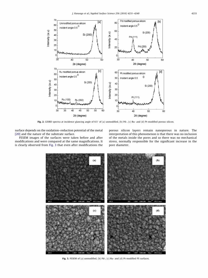
Fig. 2. GIXRD spectra at incidence glancing angle of 0.58 of (a) unmodified, (b) Pd-, (c) Ru- and (d) Pt-modified porous silicon.
J. Kanungo et al. / Applied Surface Science 256 (2010) 4231–4240 4233
surface depends on the oxidation–reduction potential of the metal[20] and the nature of the substrate surface.
FESEM images of the surfaces were taken before and aftermodifications and were compared at the same magnifications. Itis clearly observed from Fig. 3 that even after modifications the
Fig. 3. FESEM of (a) unmodified, (b) Pd-, (c
porous silicon layers remain nanoporous in nature. Theinterpretation of this phenomenon is that there was no inclusionof the metals inside the pores and so there was no mechanicalstress, normally responsible for the significant increase in thepore diameter.
) Ru- and (d) Pt-modified PS surfaces.

Fig. 4. EDX of (a) unmodified, (b) Pd-, (c) Ru- and (d) Pt-modified porous silicon surfaces.
J. Kanungo et al. / Applied Surface Science 256 (2010) 4231–42404234
Fig. 4 shows the EDX of the untreated and the noble metal-treated porous silicon surfaces. It confirms the presence of Pd, Ruand Pt in the respective modified samples. However, the presenceof Pd is more intense than the other two metals as alreadymentioned. It is also observed that there is an increase of oxygenpeak after the modification. So it is supported from EDX analysisthat the oxidation of PS surface occurs during the metaldispersions. This is corroborated with the chemical reactionsduring the treatment with the noble metal ions as shown above.However, the descending oxygen peak height from Pd to Ru to Ptindicates the reducing oxide formation.
Fig. 5. EDX line scan intensity distribution (nanoscale)
The EDX line scan intensity distribution with nanolevelresolution is shown in Fig. 5. It indicates once again a discontinu-ous dispersion of the noble metals on PS surface. The density ofdispersed Pd is higher than that of the other two metals and it isfurther supported by the values of the atomic percentage of noblemetals over the PS surface, as obtained from EDX analysis. Thevalues are 0.93 for Pd, 0.24 for Ru and 0.05 for Pt. Distribution of thenoble metals on PS surface was studied using digital X-ray imagemapping [22] and is shown in Fig. 6. It is observed that metals aremore or less uniformly dispersed over the PS nanostructure.However, the distribution density of Pd is higher compared to that
of (a) Pd-, (b) Ru- and (c) Pt-modified PS surfaces.

Fig. 6. Digital X-ray image mapping of (a) Pd-, (b) Ru- and (c) Pt-modified PS surfaces.
Fig. 7. Surface [(a-1) and (a-2)] and cross-sectional [(b-1) and (b-2)] EDX line scan analysis of Pd-modified porous silicon.
J. Kanungo et al. / Applied Surface Science 256 (2010) 4231–4240 4235

Fig. 8. Surface [(a-1) and (a-2)] and cross-sectional [(b-1) and (b-2)] EDX line scan analysis of Ru-modified porous silicon.
Fig. 9. Surface [(a-1) and (a-2)] and cross-sectional [(b-1) and (b-2)] EDX line scan analysis of Pt-modified porous silicon.
J. Kanungo et al. / Applied Surface Science 256 (2010) 4231–42404236

Fig. 10. SIMS analysis of (a) unmodified, (b) Pd-, (c) Ru- and (d) Pt-modified porous silicon.
J. Kanungo et al. / Applied Surface Science 256 (2010) 4231–4240 4237
of Ru and Pt due to the more favorable oxidation–reductionpotential for Pd, as mentioned earlier. After modifications anagglomeration of the deposited noble metals of micron size wasobserved on the PS surface. For qualitative depth profiling, thetransverse section was investigated with EDX line scanning using
Fig. 11. AFM images of unmodified porous silicon.
Genesis EDAX Line Scan software at 20 kV and at differentmagnifications suitable for identifying the metal particles/clusters.From Figs. 7a, 8a and 9a it is evident that the diameter of a typicallyagglomerated Pd island is �5.8 mm whereas a reduction in size isobserved for Ru- (�4.2 mm) and Pt- (�3.1 mm) modified samples.
Fig. 12. AFM images of Pd-modified porous silicon.

Fig. 13. AFM images of Ru-modified porous silicon. Fig. 14. AFM images of Pt-modified porous silicon.
J. Kanungo et al. / Applied Surface Science 256 (2010) 4231–42404238
The Pd agglomerates are more frequently distributed over theuniform nanostructure of PS compared to that of Ru and Pt. Linescan analysis across the cross-section of a PS sample confirms thatPd and Ru are clearly present in the structure and Pt is very rarelyfound. Presence of oxygen is also confirmed. From the cross-section EDX analysis in Figs. 7b, 8b and 9b the thickness of the PSlayer (from the surface to the depth where the Si intensity comes toa saturation value) was measured as �5 mm.
Accurate quantitative SIMS analysis requires internal cali-bration standards, which are not available for as preparedporous silicon and the modified samples. Therefore, only thequalitative SIMS for both the unmodified and the surface-modified PS are presented here. The SIMS measurements haveshown that at the depth >5 mm the intensity profile for all theelements are practically parallel to the x-axis. It is observed fromFig. 10 that the unmodified porous silicon samples containoxygen and fluorine (mostly near the surface) while themodified samples contain Pd or Ru or Pt in addition to oxygenand fluorine. The trace amount of fluorine and oxygen wereincluded during PS formation. The oxygen of the modifiedsamples reaches its maximum at the depth of �1.5 mm from thePS surface, indicating the formation of silicon dioxide (as wasalso confirmed by the XPS study). Beyond 1.5 mm there is asubstantial decrease in oxygen intensity and an increase in theintensity of silicon. Pd, Ru and Pt were obtained very near to thesurface region of the respective modified samples. And theintensity of Pd is higher compared to the other two metals as weobserve from Fig. 10b. There is no indication of oxide formation
Table 1Average particle size and roughness of unmodified and modified porous silicon sample
Unmodified PS Pd-m
Average particle size (nm) 76 180
Average roughness (nm) 1.93 7.
at the maximum peak height of the noble metals at the surfaceas is evident from the minimum intensity of both Si and Ointensities. As the metal intensity starts decreasing the oxidepeak takes up (Fig. 10b and c). This may be an indication of theformation of metal islands followed by oxide layer. Fig. 10ddemonstrates negligible inclusion of Pt on the PS surface.
The AFM images shown in Figs. 11–14 indicate an increase inthe roughness and an enhancement in the particle size aftersurface treatment with noble metals. However, the effect is moredominant for Pd-modified PS surface. The average particle size andthe roughness, calculated from the AFM characterizations, areshown in Table 1. The average particle size on the PS surface(76 nm) was increased by more than twice (176 nm) after the Pdtreatment while there was marginal increase after Ru and Pttreatment (91 nm and 89 nm). A statistical roughness estimate wasalso performed for the samples. The unmodified sample had anaverage roughness of 1.93 nm. The same analysis for the modifiedsamples yields an average roughness of 7.8 nm for Pd, 3.38 nm forRu and 3.35 nm for Pt. Therefore, the roughness is much higher forthe modified samples compared to the unmodified PS. However,the palladium-modified sample had an average roughness of morethan two times that of the Ru- and Pt-modified samples. This isfurther an indication that Pd islands/clusters are bigger in sizecompared to that of Ru and Pt and this might be due to highersticking co-efficient of Pd and thus higher incorporation to thenanoporous silicon surface. However, further in-depth investiga-tion is required to obtain more quantitative information. So, theAFM study clearly indicates that the noble metal modification of
s.
odified PS Ru-modified PS Pt-modified PS
91 89
8 3.38 3.35

Fig. 15. XPS analysis of unmodified and Pd-modified PS surface for (a) Si and (b) Pd, clearly showing a substantial enhancement of SiO2 after surface modification.
J. Kanungo et al. / Applied Surface Science 256 (2010) 4231–4240 4239
nanoporous silicon produces a rough surface with an enhancementof the particle size. However, the Pd-modification shows adistinctly dominant effect compared to Ru and Pt. This observationcorroborates with the enhanced gas sensing properties of Pdsurface modified PS as reported in details in our earliercommunication [23].
In Fig. 15a the XPS of the unmodified porous silicon surfaceshows a strong doublet at around 100 eV corresponding to puresilicon and a small doublet at around 103. 5 eV, which agree wellwith SiO2. The spectrum of Pd-modified surface, on the other hand,has the stronger doublet at 103.5 eV (SiO2) and the weaker one at100 eV (Si). This is in agreement with the EDX results. So it isindicated that Pd helps in the surface oxidation of porous silicon. InFig. 15b the Pd (3d) peak is clearly observed for the sample withpalladium-modified porous silicon. As expected, no palladiumcould be detected on the unmodified porous silicon sample.Additionally, it is verified from our XPS results that palladiumsilicide was not formed in spite of annealing the Pd-modified PSsample at relatively high temperature, as no peak for thecorresponding binding energy is observed. Since the modificationeffects of Ru and Pt are relatively insignificant compared to that ofPd the XPS study was undertaken only for the Pd-treated PSsamples.
We studied porous silicon surface treated with Pd, Ru and Ptand we observed from our experimental results that theincorporation of Pd on PS surface is more intense and uniformthan Ru and Pt. The agglomeration of the metals increases theroughness of the samples. The roughness is highest for Pd as the Pdagglomerates are more closely observed on the PS surfacecompared to the other two metals. Since the PS surface getsoxidized during metal incorporation, an enhancement in oxygenquantity was observed from EDX and XPS analysis. The roomtemperature oxidation of PS surface during noble metal modifica-tion stabilizes the material by passivating the surface defects of thePS and it was demonstrated during the electrical characterizationsof Pd-modified PS in our earlier publication [21]. The defect statesgenerated on nanoporous silicon surface during its formation byelectrochemical etching of crystalline silicon are primarilyresponsible for the instability and the unreliable electrical contact.The surface treatment by the noble metal ions largely passivatesthe surface defects due to the formation of a thin oxide layer. Theoxide semiconductors like ZnO and SnO2 with large density ofdangling bonds were also reported to improve the electricproperties after the surface treatment with the noble metal ions[14–15]. However, the mechanism of the surface passivation ofthe oxide materials was somewhat different than that fornanoporous silicon.
4. Conclusions
After the treatment with Pd, Ru and Pt metal ions thenanoporous silicon surface was thoroughly studied by the modernsurface characterization techniques. Pd metal showed the mostprominent effect. The dispersion of the noble metals and theformation of metal islands over the PS surface were confirmed. ThePd-modified surface showed more uniform distribution comparedto Ru and Pt. Both the particle size and the roughness of the treatedPS surface increased with a spectacular change for Pd, as indicatedby AFM study. The dynamic SIMS indicated the confinement of thenoble metals on the PS surface only. The XPS results confirmed theformation of a thin oxide layer on PS surface after the Pd treatment.
Acknowledgement
J. Kanungo thankfully acknowledges The Council of Scientific &Industrial Research (CSIR), Govt. of India, for providing a SeniorResearch Fellowship.
References
[1] A.G. Cullis, L.T. Canham, P.D.J. Calcott, The structural and luminescence propertiesof porous silicon, J. Appl. Phys. 82 (1997) 909.
[2] A.J. Read, R.J. Needs, K.J. Nash, L.T. Canham, P.D.J. Calcott, A. Qteish, First-principlescalculations of the electronic properties of silicon quantum wires, Phys. Rev. Lett.69 (1992) 1232.
[3] G. Bomchill, A. Halimaoui, R. Herino, Porous silicon: the material and its applica-tions to SOI technologies, Microelectron. Eng. 8 (1988) 293.
[4] A. Foucaran, B. Sorli, M. Garcia, F. Pascal-Delannoy, A. Giani, A. Boyer, Poroussilicon layer coupled with thermoelectric cooler: a humidity sensor, Sens. Actua-tors A 79 (2000) 189.
[5] C. Tsai, K.H. Li, J. Sarathi, J.C. Campbell, B.K. Hance, J.M. White, Thermal treatmentstudies of the photoluminescence intensity of porous silicon, Appl. Phys. Lett. 59(1991) 2814.
[6] A. Bsiesy, J.C. Vial, F. Gaspard, R. Herino, M. Ligeon, F. Muller, R. Romestain, A.Wasiela, A. Halimaoui, G. Bomchil, Photoluminescence of high porosity and ofelectrochemically oxidized porous silicon layers, Surf. Sci. (Netherlands) 254(1991) 195.
[7] V. Petrova-Koch, T. Muschik, A. Kux, B.K. Meyer, F. Koch, V. Lehmann, Rapid-thermal-oxidized porous Si�The superior photoluminescent Si, Appl. Phys. Lett.61 (1992) 943.
[8] I.N. Lees, H. Lin, C.A. Canaria, C. Gurtner, M.J. Sailor, G.M. Miskelly, Chemicalstability of porous silico surfaces electrochemically modified with functional alkylspecies, Langmuir 19 (2003) 9812.
[9] N.P. Mandal, A. Sharma, S.C. Agarwal, Improved stability of nanocrystallineporous silicon after coating with a polymer, J. Appl. Phys. 100 (2006) 024308.
[10] R.C. Anderson, R.S. Muller, C.W. Tobias, Chemical surface modification of poroussilicon, J. Electrochem. Soc. (USA) 140 (1993) 1393.
[11] J.M. Lauerhaas, M.J. Sailor, The effects of halogen exposure on the photolumines-cence of porous silicon, Mater. Res. Soc. Symp. Proc. (USA) 298 (1993) 259.
[12] D. Andsager, J. Hilliard, M.H. Nayfeh, Behavior of porous silicon emission spectraduring quenching by immersion in metal ion solutions, Appl. Phys. Lett. 64 (1994)1141.

J. Kanungo et al. / Applied Surface Science 256 (2010) 4231–42404240
[13] P. Steiner, F. Kozlowski, M. Wielunski, W. Lang, Enhanced blue-light emissionfrom an indium-treated porous silicon device, Jpn. J. Appl. Phys. 33 (1994)6075.
[14] P.K. Basu, S.K. Jana, M.K. Mitra, H. Saha, S. Basu, Hydrogen gas sensors usinganodically prepared and surface modified nanoporous ZnO thin films, Sens. Lett. 6(2008) 699.
[15] K. Chatterjee, S. Chatterjee, A. Banerjee, M. Raut, N.C. Pal, A. Sen, H.S. Maiti, Theeffect of palladium incorporation on methane sensitivity of antimony doped tindioxide, Mater. Chem. Phys. 81 (2003) 33.
[16] Jing Liqiang, Wang Baiqi, Xin Baifu, Li Shudan, Shi Keying, Cai Weimin, FuHonggang, Investigations on the surface modification of ZnO nanoparticle photo-catalyst by depositing Pd, J. Solid State Chem. 177 (2004) 4221.
[17] V. Polishchuk, E. Souteyrand, J.R. Martin, V.I. Strikha, V.A. Skryshevskya, A study ofhydrogen detection with palladium modified porous silicon, Anal. Chim. Acta 375(1998) 205.
[18] J. Kanungo, C. Pramanik, S. Bandopadhyay, U. Gangopadhyay, L. Das, H. Saha,R.T.T. Gettens, Improved contacts on porous silicon layer by electroless nickelplating and copper thickening, Semicond. Sci. Technol. 21 (2006) 964.
[19] H. Saha, S.K. Dutta, S.M. Hossain, S. Chakraborty, A Saha, Mechanism and controlof formation of porous silicon on p-type Si, Bull. Mater. Sci. 21 (3) (1998) 195.
[20] M. Jeske, J.W. Schultze, M. Thonissen, H. Munder, Electrodeposition of metals intoporous silicon, Thin Solid Films 255 (1995) 63–66.
[21] J. Kanungo, S. Maji, H. Saha, S. Basu, Stable aluminium ohmic contact to surfacemodified porous silicon, Solid State Electron. 53 (2009) 663.
[22] M. Torkiha, M. Lamehi-Rachti, D. Agha-Aligol, F. Razi, Controlled electrolessdeposition of noble metal nanoparticle films on germanium surfaces, Nucl. Instr.Methods B 266 (2008) 1507.
[23] J. Kanungo, H. Saha, S. Basu, Room temperature metal-insulator–semiconductor(MIS) hydrogen sensors based on chemically surface modified porous silicon,Sens. Actuator B Chem. 140 (2009) 65.