silicon‐based integrated label‐free optofluidic biosensors
TRANSCRIPT
www.advmattechnol.de
1901138 (1 of 24) © 2020 The Authors. Published by WILEY-VCH Verlag GmbH & Co. KGaA, Weinheim
Review
Silicon-Based Integrated Label-Free Optofluidic Biosensors: Latest Advances and Roadmap
Jiawei Wang,* Mariana Medina Sanchez, Yin Yin, Raffael Herzer, Libo Ma,* and Oliver G. Schmidt
DOI: 10.1002/admt.201901138
1. Introduction
Advancing medical diagnostic technolo-gies is crucial for identifying or preventing human disease in the early stages and per-forming effective clinical treatments. Now-adays, most of the diagnoses are conducted based on standard tests in centralized clin-ical laboratories with delicate and sophisti-cated instruments by well-trained experts. In recent years, personalized medicine has been proposed as a paradigm shift in indi-vidualized therapies, featuring monitored progress, evaluated safety, and improved efficiency. Notably, the concept of “point-of-care (POC)” diagnostics emerges with tremendous advances in compact, cost-effective, and reliable bioanalytical systems providing diagnostic testing in a very short time without sophisticated protocols.[1–3] Thus, POC diagnostics for personalized medicine is highly promising for revolu-tionizing global healthcare at the dawn of the twenty-first century.[4]
Among a large variety of medical dia-gnostic routes, discrimination and quanti-fication of specific biomarkers in biological
fluids have been known as the highly efficient way to trace the corresponding diseases. In the past 40 years, the commer-cial enzyme-linked immunosorbent assay (ELISA) serves as a standard method of biomarker detection for in vitro diagnostics.[5] However, as a fluorescence labeling-based approach, it has the fol-lowing limitations: i) need of sophisticated reagent selection and pairing; ii) complex, bulky setup for data readout, and iii) long preparation and operation time. As a consequence, label-free bio-sensing approaches become desirable to meet the demands of POC diagnostics. Surface plasmon resonance (SPR)-based bio-sensors are the most well-known and widely applied label-free optical bioanalytical tools since the first successfully commercial-ized product by Biacore 30 years ago.[6,7] Since then, numerous efforts on label-free optical biosensors have been invested,[8] which cover different types of optical measurements such as transmission,[9,10] emission,[11] adsorption,[12] polarimetry,[13] and light scattering.[14] These sensing techniques reveal potential applications not only in medical diagnostics but also in drug dis-covery,[15] food safety,[16,17] and environmental monitoring.[18]
Over the past decades, different miniaturized architectures fabricated on a chip have been continuously explored in various
By virtue of the well-developed micro- and nanofabrication technologies and rapidly progressing surface functionalization strategies, silicon-based devices have been widely recognized as a highly promising platform for the next-gener-ation lab-on-a-chip bioanalytical systems with a great potential for point-of-care medical diagnostics. Herein, an overview of the latest advances in silicon-based integrated optofluidic label-free biosensing technologies relying on the efficient interactions between the evanescent light field at the functionalized surface and specifically bound analytes is presented. State-of-the-art technologies demonstrating label-free evanescent wave-based biomarker detection mainly encompass three device configurations, including on-chip waveguide-based interferometers, microring resonators, and photonic-crystal-based cavities. Moreover, up-to-date strategies for elevating the sensitivities and also simpli-fying the sensing processes are discussed. Emerging laboratory prototypes with advanced integration and packaging schemes incorporating automatic microfluidic components or on-chip optoelectronic devices lead to one signifi-cant step forward in real applications of decentralized diagnostics. Besides, particular attention is paid to currently commercialized label-free optical bioana-lytical models on the market. Finally, the prospects are elaborated with several research routes toward chip-scale, low-cost, highly sensitive, multi-functional, and user-friendly bioanalytical systems benefiting to global healthcare.
Dr. J. Wang, Dr. M. M. Sanchez, Dr. Y. Yin, R. Herzer, Dr. L. MaInstitute for Integrative NanosciencesLeibniz IFW DresdenDresden 01069, GermanyE-mail: [email protected]; [email protected]. J. Wang, Prof. O. G. SchmidtMaterial Systems for NanoelectronicsTechnische Universität ChemnitzChemnitz 09107, GermanyDr. J. Wang, Prof. O. G. SchmidtResearch Center for MaterialsArchitectures and Integration of NanomembranesTechnische Universität ChemnitzRosenbergstrasse 6, Chemnitz 09126, Germany
The ORCID identification number(s) for the author(s) of this article can be found under https://doi.org/10.1002/admt.201901138.
Hall of Fame Article
Adv. Mater. Technol. 2020, 5, 1901138
© 2020 The Authors. Published by WILEY-VCH Verlag GmbH & Co. KGaA, Weinheim. This is an open access article under the terms of the Creative Commons Attribution-NonCommercial License, which permits use, distribution and reproduction in any medium, provided the original work is properly cited and is not used for commercial purposes.
www.advancedsciencenews.com www.advmattechnol.de
1901138 (2 of 24) © 2020 The Authors. Published by WILEY-VCH Verlag GmbH & Co. KGaA, Weinheim
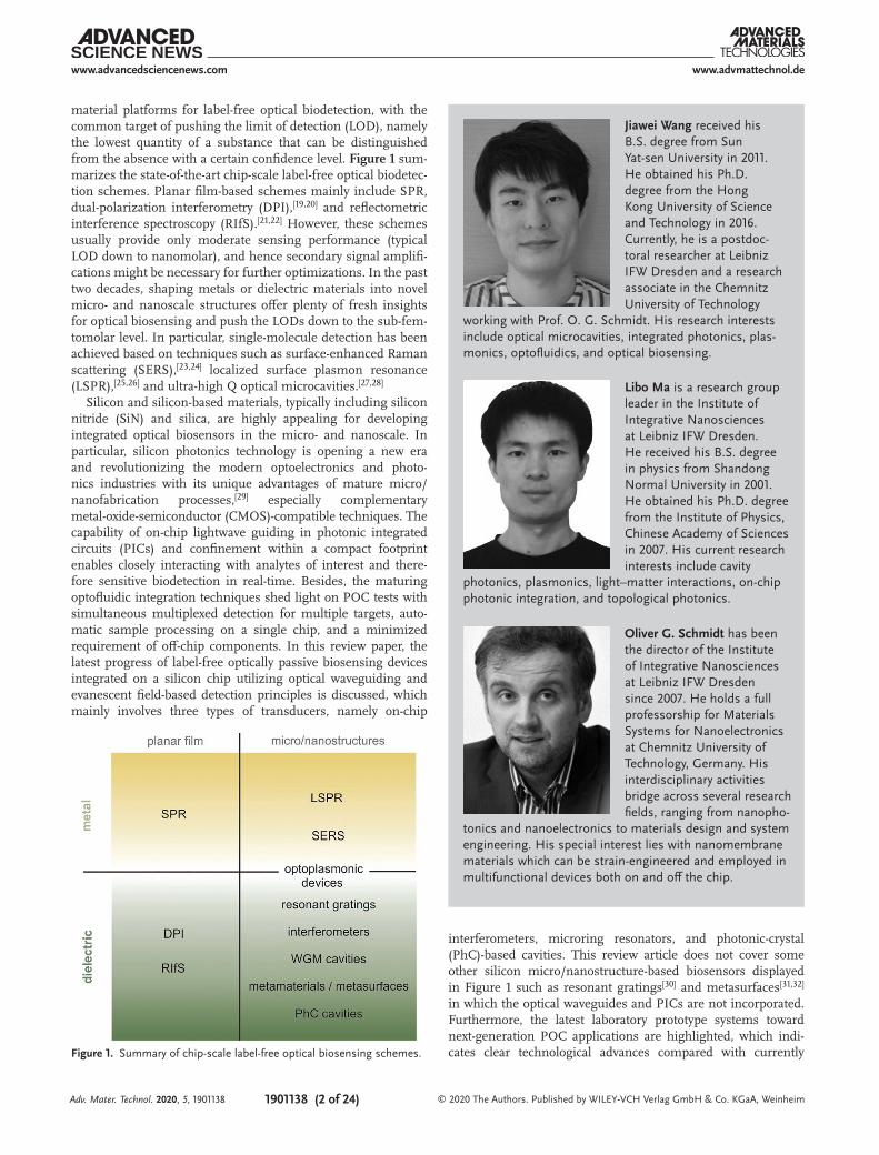
material platforms for label-free optical biodetection, with the common target of pushing the limit of detection (LOD), namely the lowest quantity of a substance that can be distinguished from the absence with a certain confidence level. Figure 1 sum-marizes the state-of-the-art chip-scale label-free optical biodetec-tion schemes. Planar film-based schemes mainly include SPR, dual-polarization interferometry (DPI),[19,20] and reflectometric interference spectroscopy (RIfS).[21,22] However, these schemes usually provide only moderate sensing performance (typical LOD down to nanomolar), and hence secondary signal amplifi-cations might be necessary for further optimizations. In the past two decades, shaping metals or dielectric materials into novel micro- and nanoscale structures offer plenty of fresh insights for optical biosensing and push the LODs down to the sub-fem-tomolar level. In particular, single-molecule detection has been achieved based on techniques such as surface-enhanced Raman scattering (SERS),[23,24] localized surface plasmon resonance (LSPR),[25,26] and ultra-high Q optical microcavities.[27,28]
Silicon and silicon-based materials, typically including silicon nitride (SiN) and silica, are highly appealing for developing integrated optical biosensors in the micro- and nanoscale. In particular, silicon photonics technology is opening a new era and revolutionizing the modern optoelectronics and photo-nics industries with its unique advantages of mature micro/nanofabrication processes,[29] especially complementary metal-oxide-semiconductor (CMOS)-compatible techniques. The capability of on-chip lightwave guiding in photonic integrated circuits (PICs) and confinement within a compact footprint enables closely interacting with analytes of interest and there-fore sensitive biodetection in real-time. Besides, the maturing optofluidic integration techniques shed light on POC tests with simultaneous multiplexed detection for multiple targets, auto-matic sample processing on a single chip, and a minimized requirement of off-chip components. In this review paper, the latest progress of label-free optically passive biosensing devices integrated on a silicon chip utilizing optical waveguiding and evanescent field-based detection principles is discussed, which mainly involves three types of transducers, namely on-chip
Jiawei Wang received his B.S. degree from Sun Yat-sen University in 2011. He obtained his Ph.D. degree from the Hong Kong University of Science and Technology in 2016. Currently, he is a postdoc-toral researcher at Leibniz IFW Dresden and a research associate in the Chemnitz University of Technology
working with Prof. O. G. Schmidt. His research interests include optical microcavities, integrated photonics, plas-monics, optofluidics, and optical biosensing.
Libo Ma is a research group leader in the Institute of Integrative Nanosciences at Leibniz IFW Dresden. He received his B.S. degree in physics from Shandong Normal University in 2001. He obtained his Ph.D. degree from the Institute of Physics, Chinese Academy of Sciences in 2007. His current research interests include cavity
photonics, plasmonics, light–matter interactions, on-chip photonic integration, and topological photonics.
Oliver G. Schmidt has been the director of the Institute of Integrative Nanosciences at Leibniz IFW Dresden since 2007. He holds a full professorship for Materials Systems for Nanoelectronics at Chemnitz University of Technology, Germany. His interdisciplinary activities bridge across several research fields, ranging from nanopho-
tonics and nanoelectronics to materials design and system engineering. His special interest lies with nanomembrane materials which can be strain-engineered and employed in multifunctional devices both on and off the chip.
interferometers, microring resonators, and photonic-crystal (PhC)-based cavities. This review article does not cover some other silicon micro/nanostructure-based biosensors displayed in Figure 1 such as resonant gratings[30] and metasurfaces[31,32] in which the optical waveguides and PICs are not incorporated. Furthermore, the latest laboratory prototype systems toward next-generation POC applications are highlighted, which indi-cates clear technological advances compared with currently
Adv. Mater. Technol. 2020, 5, 1901138
Figure 1. Summary of chip-scale label-free optical biosensing schemes.
www.advancedsciencenews.com www.advmattechnol.de
1901138 (3 of 24) © 2020 The Authors. Published by WILEY-VCH Verlag GmbH & Co. KGaA, Weinheim
commercialized technologies. At last, we discuss the future research directions and development roadmap for silicon-based label-free optical biosensors toward ultimately ultra-sensitive, multi-functional, and portable bioanalytical systems.
2. Silicon Photonics for Label-Free Biosensing
2.1. Silicon-Based Material Platform
Compared to other alternative material platforms for developing PICs and integrated optical sensors, such as polymer,[33,34] aluminum oxide,[35] III-V materials,[36] and lithium niobate,[37] silicon features a high-precision, low-cost, and high-yield device fabrication with good reproducibility owing to the mature CMOS processes.[38,39] Table 1 summarizes the optical properties of common silicon-based materials. In the silicon-on-insulator (SOI) platform, the top silicon layer with sub-wavelength thickness serves as the optical waveguiding medium for near-infrared (IR) light (mostly at telecommunication band). However, the telecom-munication wavelength leads to serious water absorption, which makes it not ideal for biomedical research and applications.
The ultra-wide transparency window from visible to mid-IR renders SiN a versatile option for tremendous emerging appli-cations ranging from 3D PICs,[40] nonlinear photonics[41] to bio-photonics.[41–43] The SiN-on-silica platform indicates a sufficiently large refractive index contrast and thus tight optical confinement in compact device footprints. Nowadays, multiple commercial foundry platforms including LioniX’s TriPleX,[44] Ligentec’s Dam-ascene,[45] IMEC’s BioPIX,[46] and the IMB-CNM[46] aim at devel-oping SiN-based integrated photonic technologies with ultra-low propagation loss (<1 dB m−1).[42] In particular, the operation wave-length at the visible or near-IR (<1.1 µm) range naturally takes the advantage of ubiquitous and low-cost light sources such as light-emitting diodes (LEDs) or laser diodes, and readout compo-nents such as silicon/germanium-based photodetectors (PDs) or CCD/CMOS cameras.[47] In addition, SiN-based photonic devices reveal a less susceptibility to temperature variation due to its relatively small thermo-optic coefficient compared to silicon,[48] which is advantageous for suppressing the environmental noises and improving the stability in sensing tests.
2.2. Optofluidic Integrations for Silicon-Based Biosensors
As a nascent field integrating micro/nanofluidics and optical/photonic technologies, optofluidics opens up remarkable pos-sibilities for fundamental science and applications.[49,50] For
biomedical-related studies, it offers a key route to break new ground on multi-functional “lab-on-a-chip” systems with a small footprint, streamlined protocol, low required sample volume, and ideally high throughput.[51–55]
Various straightforward and convenient methods have been developed for integrating silicon-based materials with microfluidic components.[56] Polydimethylsiloxane (PDMS) as a low-cost, easy-to-use, optically transparent and biocompat-ible material is popular in the field of micro/nanofluidics with the capability of building complex 3D microfluidic circuits.[57] PDMS can be molded using, for example, SU8-masters,[58] methacrylate-mechanized molds,[59] 3D printed molds[60] (i.e., wax printing channels[61]), among others. It is easy to replicate, by mixing the elastomer and catalyzer, typically in a propor-tion 10:1, poured it on the respective mold and let it solidify upon an applied temperature (≈60 °C) for a couple of hours. The mechanical and optical properties of PDMS can be tuned by changing the proportion between elastomer and catalyzer, the curing conditions, or by incorporating nanomaterials[62] or other functional powders within the elastomer, prior molding.[63] The PDMS-based microfluidic layer can be per-manently bound to silica after oxygen plasma treatment due to hydrogen bonding. A thin layer of ethanol solution between the two surfaces prior to bonding might facilitate the precise alignment between PDMS and the silicon chip under optical microscopy.[64] This integration serves as the most common way to introduce fluidic channels to silicon-based optical bio-sensors for sample delivery and bioconjugation tasks.[65,66] However, there are some drawbacks of optofluidic integrated biosensing using PDMS-based channels, including non-spe-cific adsorption of hydrophobic molecules,[67] deformation in nonpolar organic solvents (e.g., toluene),[68] and difficulty for unmounting the PDMS layer from the chip due to the irrevers-ible bonding. There are alternatives to reduce unspecific adhe-sion to the PDMS surface. For example, small molecule pro-teins such as ethanolamine or casein,[69] or polymers such as polyethylene glycol (PEG)[70] can be applied to cover the PDMS surface prior to detection.
Aside from PDMS, SU-8 as a widely used negative photore-sist in microelectronic industries is also commonly employed for microfluidic channels. It is a biocompatible material with good transparency in a wide spectrum range. Owing to the standard lithography process, it offers a precision alignment between the on-chip devices and microfluidic channels.[71] SU-8 channels can be directly patterned onto the sensor sur-face with high precision at different heights in a single step by using multi-wavelength lithography,[72] in particular when a fine interconnection is required between the fluidic inlet/outlet and
Adv. Mater. Technol. 2020, 5, 1901138
Table 1. Optical properties of common materials involved in the silicon photonics technology.
Materials Silicon Silicon nitride (Stoichiometric Si3N4 as an example) Silicon dioxide
Bandgap 1.12 eV ≈5eV ≈9 eV
Transparency window 1.1 – 9 µm 0.25–8 µm 0.13–3.5 µm
Refractive index @ 600 nm 3.95 ≈2.04 ≈1.46
Refractive index @ 1550 nm 3.67 ≈2 ≈1.44
Fabrication process Crystal material/commercially available SOI wafer LPCVD/PECVD Thermal growth, PVD, CVD
PVD, physical vapor deposition; CVD, chemical vapor deposition; LPCVD, low-pressure chemical vapor deposition; PECVD, plasma-enhanced chemical vapor deposition.
www.advancedsciencenews.com www.advmattechnol.de
1901138 (4 of 24) © 2020 The Authors. Published by WILEY-VCH Verlag GmbH & Co. KGaA, Weinheim
the sensor device. As a drawback, SU-8 has to be processed in a cleanroom and several processing steps must be conducted for achieving a multilayer platform that consumes more time in comparison with replicated PDMS platforms.[73] Some other UV curable polymers (e.g., NOA 61, NOA 81) have also been adopted for fabricating microfluidic channels.[74] NOA 63, an optical adhesive, could be used as a substitute to PDMS offering high reproducibility and native hydrophilicity.[75] In addition to polymers, silica-based fluidic channels exhibit good material properties concerning their structural stability, chemical inert-ness, and a low adsorption rate for ambient molecules.[76,77] Moreover, they can be fabricated rapidly with low cost in a wafer-scale by standard lithography and etching process.
2.3. Surface Functionalization Strategies
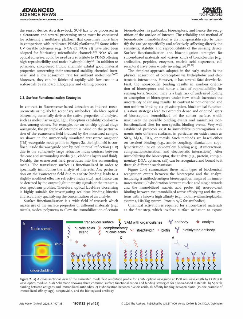
In contrast to fluorescence-based detection as indirect meas-urements using labeled secondary antibodies, label-free optical biosensing essentially derives the native properties of analytes, such as molecular weight, light absorption capability, conforma-tion, among others. For example, for an on-chip optical ridge waveguide, the principle of detection is based on the perturba-tion of the evanescent field induced by the measured sample. As shown in the numerically simulated transverse magnetic (TM) waveguide mode profile in Figure 2a, the light field is con-fined inside the waveguide core by total internal reflection (TIR) due to the sufficiently large refractive index contrast between the core and surrounding media (i.e., cladding layers and fluid). Notably, the evanescent field penetrates into the surrounding media. The transducer surface is functionalized in order to specifically immobilize the analyte of interests. Any perturba-tion on the evanescent field due to analyte binding leads to a slightly modified effective refractive index (neff), and hence can be detected by the output light intensity signals or the transmis-sion spectrum profiles. Therefore, optical label-free biosensing is highly suitable for investigating real-time binding kinetics and accurately quantifying the concentration of an analyte.
Surface functionalization is a wide field of research which makes use of the surface properties of different materials (e.g., metals, oxides, polymers) to allow the immobilization of certain
biomolecules, in particular, bioreceptors, and hence the recog-nition of the analyte of interest. The reliability and method of biomolecule immobilization is an indispensable step to iden-tify the analyte specifically and selectively, affecting directly the sensitivity, stability, and reproducibility of the sensing device. Surface functionalization and bioconjugation strategies for silicon-based materials and various kinds of biomolecules (e.g., antibodies, peptides, enzymes, nucleic acid sequences, cell receptors) have been widely investigated.[78,79]
The simplest approach adopted in the early studies is the physical adsorption of bioreceptors via hydrophobic and elec-trostatic interactions. However, it has several fatal drawbacks. First, the non-specific binding results in random orienta-tion of bioreceptors and hence a lack of reproducibility for sensing tests. Second, there is a high risk of undesired folding or desorption of bioreceptors under flow, which increases the uncertainty of sensing results. In contrast to non-oriented and non-uniform binding via physisorption, biochemical function-alization strategies lead to extremely dense and oriented layers of bioreceptors immobilized on the sensor surface, which maximizes the possible binding events and minimizes non-functionalized sites for non-specific binding events. Very well established protocols exist to immobilize biorecognition ele-ments onto different surfaces, in particular on oxides such as SiO2, Al2O3, TiO2, or metals. Such methods are based either on covalent binding (e.g., amide coupling, silanization, copo-lymerization), or on non-covalent binding (e.g., π interactions, complexation/chelation, and electrostatic interactions). After immobilizing the bioreceptor, the analyte (e.g., protein, comple-mentary DNA, aptamer, cell) can be recognized and bound to it through different mechanisms.
Figure 2b–d summarizes three main types of biochemical recognition events between the bioreceptor and the analyte, including i) antibody-antigen biorecognition inspired in immu-noreactions; ii) hybridization between nucleic acid single strands and the immobilized nucleic acid probe; iii) non-covalent binding between the immobilized active affinity tag and the sys-tems with a known high affinity (e.g., biotin-avidin/streptavidin systems, His-Tag system, Protein A/G for antibodies).
Chemical activation is required for silicon-based materials as the first step, which involves surface oxidation to expose
Adv. Mater. Technol. 2020, 5, 1901138
Figure 2. a) A cross-sectional view of the simulated mode field amplitude profile for a SiN optical waveguide at 1550 nm wavelength by COMSOL wave optics module. b–d) Schematic showing three common surface functionalization and binding strategies for silicon-based materials. b) Specific binding between antigens and immobilized antibodies. c) Hybridization between nucleic acids. d) Affinity binding between biotin (as one example of immobilized affinity tags), streptavidin, and the biotinylated antibody.
www.advancedsciencenews.com www.advmattechnol.de
1901138 (5 of 24) © 2020 The Authors. Published by WILEY-VCH Verlag GmbH & Co. KGaA, Weinheim
the silanol groups for cross-linking with the organosilanes.[80] For SiN, an etching of the native oxide layer followed by thermal oxidation is favored. To increase the density of reac-tive hydroxyl (-OH) groups, oxygen plasma or chemical treat-ment (e.g., using piranha solution) are usually adopted. The activated surface is ready for salinization with the exposed reactive groups susceptible to reaction with specific biorecep-tors. Researchers have developed hundreds of organosilanes with different functional groups, such as amino (-NH2), car-boxylic (-COOH), and thiol (-SH) for protein/enzyme/nucleic acid binding. As a widely adopted method, (3-Aminopropyl)-triethoxysilane interacting with the surface hydroxyl groups leads to highly stable, oriented self-assembled monolayers covalently bonded on the surface (see Figure 2b). For immobi-lization of nucleic acid probes in Figure 2c, the incorporation of reactive groups at the end of the nucleic acid sequence is required during the synthesis.[81,82]
Regarding non-covalent affinity binding strategies, one well-established method is based on the biotin-avidin/strepta-vidin system via a sandwich-like assay (biotin immobilized on the sensor surface/(strep)avidin/biotinylated biomolecule, see Figure 2d).[83] The (strep)avidin-biotin complex is the strongest known non-covalent interaction between a protein and ligand. As a consequence, it is also widely adopted for proof-of-concept demonstrations in optical biosensors.[84,85] Recently, monolayer graphene was utilized by integration on top of silicon micro-rings for efficiently detection molecule adsorption (e.g., dopamine) by π stacking.[86]
Medical diagnostics requires the identification and quan-tification of specific disease biomarkers in real biofluids.[87] Table 2 summarizes currently developed silicon-based
surface-functionalized optical biosensors with demonstrated label-free detection of corresponding biomarkers for disease diagnostics. Notably, complex human biofluid samples (e.g., blood, urine, serum, saliva, sputum, tears, and sweat) con-tain a large number of other molecules. The potential non-specific binding may lead to a complicated background or false signals.[88] Therefore, blocking the “free” sites without bioreceptors with inert molecules should be implemented for suppressing the occurrence of non-specific binding and hence ensuring sensing with high specificity. Blocking com-pounds in conventional biosensing tests includes bovine serum albumin,[89] fish gelatin,[90] and Tween 20.[91] However, this method may still face problems for sensing in plasma or serum samples. Functionalizable antifouling coatings have been continuously explored to minimize the non-specific binding and improve sensing accuracy.[88]
3. Silicon-Based Label-Free Optical Biosensors
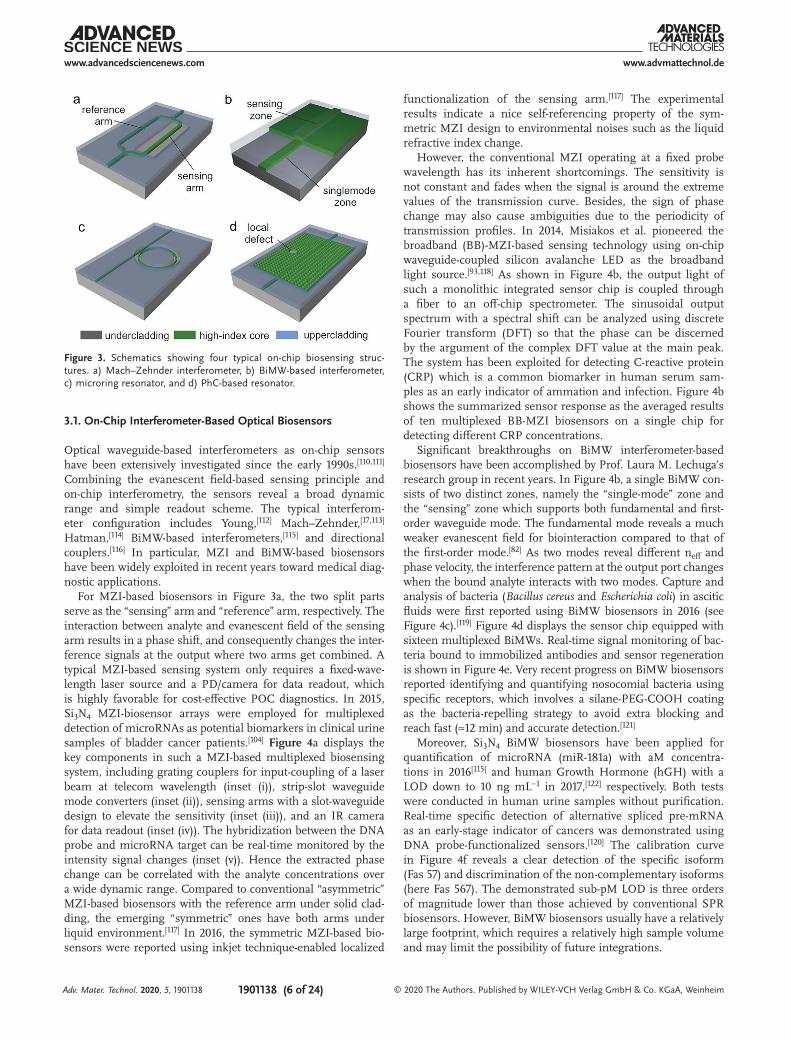
In this section, we present an overview of the latest achieve-ments on silicon-based label-free optical biosensors. Figure 3 summarizes four representative photonic structures for evanescent field-based sensing, including Mach–Zehnder interferometer (MZI), bimodal waveguide (BiMW)-based interferometer, microring resonator, and PhC-based cavity. The detailed sensing principles have been clearly explained in previous review articles.[73,106–109] Here we focus on the latest breakthroughs in pushing the sensing performance, extending the functionalities, and simplifying the sensing protocols.
Adv. Mater. Technol. 2020, 5, 1901138
Table 2. Summary of disease biomarkers existing in body fluids discriminated and quantified by state-of-the-art silicon-based label-free optical bio-sensing techniques.
Application on diagnostics Biomarker Fluid Receptor/target Device configuration
Detection limit Ref.
Acute inflammation C-reactive protein (CRP) Serum and plasma Anti-CRP Microring ≈200 fm [92]
Acute inflammation CRP Serum Anti-CRP BB-MZI ≈2.1 ng mL−1 [93]
Acute inflammation CRP Buffer solution Anti-CRP BB-MZI ≈19 ng mL−1 [94]
Infections and inflammatory diseases
Cytokines interleukin (IL) 2,4,5 Serum-containing cell media Anti-IL 2,4,5 Microring 6–100 pm [95]
Meningitis Bacterial transfer-messenger RNA (tmRNA)
Buffer solution Complementary ssDNA Microring 53 fm [96]
Tuberculosis Lipoarabinomannan (LAM) Urine Anti-LAM BB-MZI ≈27 pm [97]
Tuberculosis Single-stranded DNA (IS6110) Sputum Single-stranded DNA (IS6110 and IS1081)
Microring 5 fg uL−1 [98]
Breast cancer Human epidermal growth factor receptor 2 (HER2)
Buffer solution Anti-HER2 Microring 2.5 µg mL−1 [99]
Lung cancer ZEB1 gene in the lysates Whole cell lysate Anti-ZEB1 PhC 1 cell mL−1 [100]
Prostate cancer Prostate specific antigen (PSA) Buffer solution Anti-PSA Microring 0.4 nm [101]
Bowel cancer Carcinoembryonic antigen (CEA) Serum Anti-CEA Microring 10 pm [102]
Pancreatic cancer Hepatic growth factor, chemokine ligand 4, fas ligand
Serum Antibodies (not specified) PhC 3 fm [103]
Bladder cancer 2 miRNA Urine Complementary DNA Slot MZI ≈1 nm [104]
HIV Human immunoglobulin (Hu-IgG) Goat serum Anti-Hu-lgG Microring 1 ng [105]
www.advancedsciencenews.com www.advmattechnol.de
1901138 (6 of 24) © 2020 The Authors. Published by WILEY-VCH Verlag GmbH & Co. KGaA, Weinheim
3.1. On-Chip Interferometer-Based Optical Biosensors
Optical waveguide-based interferometers as on-chip sensors have been extensively investigated since the early 1990s.[110,111] Combining the evanescent field-based sensing principle and on-chip interferometry, the sensors reveal a broad dynamic range and simple readout scheme. The typical interferom-eter configuration includes Young,[112] Mach–Zehnder,[17,113] Hatman,[114] BiMW-based interferometers,[115] and directional couplers.[116] In particular, MZI and BiMW-based biosensors have been widely exploited in recent years toward medical diag-nostic applications.
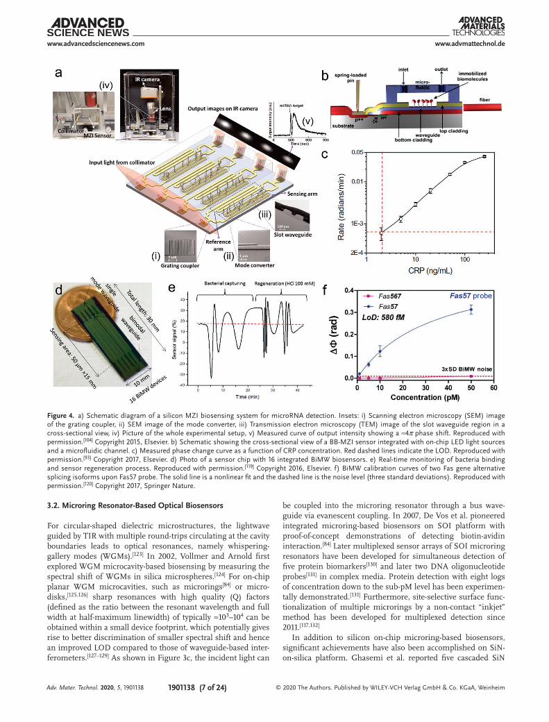
For MZI-based biosensors in Figure 3a, the two split parts serve as the “sensing” arm and “reference” arm, respectively. The interaction between analyte and evanescent field of the sensing arm results in a phase shift, and consequently changes the inter-ference signals at the output where two arms get combined. A typical MZI-based sensing system only requires a fixed-wave-length laser source and a PD/camera for data readout, which is highly favorable for cost-effective POC diagnostics. In 2015, Si3N4 MZI-biosensor arrays were employed for multi plexed detection of microRNAs as potential biomarkers in clinical urine samples of bladder cancer patients.[104] Figure 4a displays the key components in such a MZI-based multiplexed biosensing system, including grating couplers for input-coupling of a laser beam at telecom wavelength (inset (i)), strip-slot waveguide mode converters (inset (ii)), sensing arms with a slot-waveguide design to elevate the sensitivity (inset (iii)), and an IR camera for data readout (inset (iv)). The hybridization between the DNA probe and microRNA target can be real-time monitored by the intensity signal changes (inset (v)). Hence the extracted phase change can be correlated with the analyte concentrations over a wide dynamic range. Compared to conventional “asymmetric” MZI-based biosensors with the reference arm under solid clad-ding, the emerging “symmetric” ones have both arms under liquid environment.[117] In 2016, the symmetric MZI-based bio-sensors were reported using inkjet technique-enabled localized
functionalization of the sensing arm.[117] The experimental results indicate a nice self-referencing property of the sym-metric MZI design to environmental noises such as the liquid refractive index change.
However, the conventional MZI operating at a fixed probe wavelength has its inherent shortcomings. The sensitivity is not constant and fades when the signal is around the extreme values of the transmission curve. Besides, the sign of phase change may also cause ambiguities due to the periodicity of transmission profiles. In 2014, Misiakos et al. pioneered the broadband (BB)-MZI-based sensing technology using on-chip waveguide-coupled silicon avalanche LED as the broadband light source.[93,118] As shown in Figure 4b, the output light of such a monolithic integrated sensor chip is coupled through a fiber to an off-chip spectrometer. The sinusoidal output spectrum with a spectral shift can be analyzed using discrete Fourier transform (DFT) so that the phase can be discerned by the argument of the complex DFT value at the main peak. The system has been exploited for detecting C-reactive protein (CRP) which is a common biomarker in human serum sam-ples as an early indicator of ammation and infection. Figure 4b shows the summarized sensor response as the averaged results of ten multiplexed BB-MZI biosensors on a single chip for detecting different CRP concentrations.
Significant breakthroughs on BiMW interferometer-based biosensors have been accomplished by Prof. Laura M. Lechuga’s research group in recent years. In Figure 4b, a single BiMW con-sists of two distinct zones, namely the “single-mode” zone and the “sensing” zone which supports both fundamental and first-order waveguide mode. The fundamental mode reveals a much weaker evanescent field for biointeraction compared to that of the first-order mode.[82] As two modes reveal different neff and phase velocity, the interference pattern at the output port changes when the bound analyte interacts with two modes. Capture and analysis of bacteria (Bacillus cereus and Escherichia coli) in ascitic fluids were first reported using BiMW biosensors in 2016 (see Figure 4c).[119] Figure 4d displays the sensor chip equipped with sixteen multiplexed BiMWs. Real-time signal monitoring of bac-teria bound to immobilized antibodies and sensor regeneration is shown in Figure 4e. Very recent progress on BiMW biosensors reported identifying and quantifying nosocomial bacteria using specific receptors, which involves a silane-PEG-COOH coating as the bacteria-repelling strategy to avoid extra blocking and reach fast (≈12 min) and accurate detection.[121]
Moreover, Si3N4 BiMW biosensors have been applied for quantification of microRNA (miR-181a) with aM concentra-tions in 2016[115] and human Growth Hormone (hGH) with a LOD down to 10 ng mL−1 in 2017,[122] respectively. Both tests were conducted in human urine samples without purification. Real-time specific detection of alternative spliced pre-mRNA as an early-stage indicator of cancers was demonstrated using DNA probe-functionalized sensors.[120] The calibration curve in Figure 4f reveals a clear detection of the specific isoform (Fas 57) and discrimination of the non-complementary isoforms (here Fas 567). The demonstrated sub-pM LOD is three orders of magnitude lower than those achieved by conventional SPR biosensors. However, BiMW biosensors usually have a relatively large footprint, which requires a relatively high sample volume and may limit the possibility of future integrations.
Adv. Mater. Technol. 2020, 5, 1901138
Figure 3. Schematics showing four typical on-chip biosensing struc-tures. a) Mach–Zehnder interferometer, b) BiMW-based interferometer, c) microring resonator, and d) PhC-based resonator.
www.advancedsciencenews.com www.advmattechnol.de
1901138 (7 of 24) © 2020 The Authors. Published by WILEY-VCH Verlag GmbH & Co. KGaA, Weinheim
3.2. Microring Resonator-Based Optical Biosensors
For circular-shaped dielectric microstructures, the lightwave guided by TIR with multiple round-trips circulating at the cavity boundaries leads to optical resonances, namely whispering-gallery modes (WGMs).[123] In 2002, Vollmer and Arnold first explored WGM microcavity-based biosensing by measuring the spectral shift of WGMs in silica microspheres.[124] For on-chip planar WGM microcavities, such as microrings[84] or micro-disks,[125,126] sharp resonances with high quality (Q) factors (defined as the ratio between the resonant wavelength and full width at half-maximum linewidth) of typically ≈103–104 can be obtained within a small device footprint, which potentially gives rise to better discrimination of smaller spectral shift and hence an improved LOD compared to those of waveguide-based inter-ferometers.[127–129] As shown in Figure 3c, the incident light can
be coupled into the microring resonator through a bus wave-guide via evanescent coupling. In 2007, De Vos et al. pioneered integrated microring-based biosensors on SOI platform with proof-of-concept demonstrations of detecting biotin-avidin interaction.[84] Later multiplexed sensor arrays of SOI microring resonators have been developed for simultaneous detection of five protein biomarkers[130] and later two DNA oligonucleotide probes[131] in complex media. Protein detection with eight logs of concentration down to the sub-pM level has been experimen-tally demonstrated.[131] Furthermore, site-selective surface func-tionalization of multiple microrings by a non-contact “inkjet” method has been developed for multiplexed detection since 2011.[117,132]
In addition to silicon on-chip microring-based biosensors, significant achievements have also been accomplished on SiN-on-silica platform. Ghasemi et al. reported five cascaded SiN
Adv. Mater. Technol. 2020, 5, 1901138
Figure 4. a) Schematic diagram of a silicon MZI biosensing system for microRNA detection. Insets: i) Scanning electron microscopy (SEM) image of the grating coupler, ii) SEM image of the mode converter, iii) Transmission electron microscopy (TEM) image of the slot waveguide region in a cross-sectional view, iv) Picture of the whole experimental setup, v) Measured curve of output intensity showing a ≈4π phase shift. Reproduced with permission.[104] Copyright 2015, Elsevier. b) Schematic showing the cross-sectional view of a BB-MZI sensor integrated with on-chip LED light sources and a microfluidic channel. c) Measured phase change curve as a function of CRP concentration. Red dashed lines indicate the LOD. Reproduced with permission.[93] Copyright 2017, Elsevier. d) Photo of a sensor chip with 16 integrated BiMW biosensors. e) Real-time monitoring of bacteria binding and sensor regeneration process. Reproduced with permission.[119] Copyright 2016, Elsevier. f) BiMW calibration curves of two Fas gene alternative splicing isoforms upon Fas57 probe. The solid line is a nonlinear fit and the dashed line is the noise level (three standard deviations). Reproduced with permission.[120] Copyright 2017, Springer Nature.
www.advancedsciencenews.com www.advmattechnol.de
1901138 (8 of 24) © 2020 The Authors. Published by WILEY-VCH Verlag GmbH & Co. KGaA, Weinheim
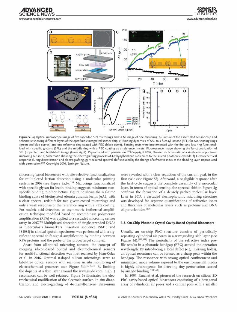
microring-based biosensors with site-selective functionalization for multiplexed lection detection using a molecular printing system in 2016 (see Figure 5a,b).[133] Microrings functionalized with specific glycan for lectin binding suggests minimum non-specific binding to other lectins. Figure 5c shows the real-time binding curve of biotinylated Aleuria aurantia lectin (AAL) with a clear spectral redshift for two glycan-coated microrings and only a weak response of the reference ring with a PEG coating. For nucleic acid detection, an asymmetric isothermal amplifi-cation technique modified based on recombinase polymerase amplification (RPA) was applied to a cascaded microring sensor array in 2017.[98] Multiplexed detection of single-stranded DNAs as tuberculosis biomarkers (insertion sequence IS6110 and IS1081) in clinical sputum specimens was performed with a sig-nificant spectral shift signal amplification by binding between RPA proteins and the probe or the probe/target complex.
Apart from all-optical microring sensors, the concept of merging silicon-based optical and electrochemical sensors for multi-functional detection was first realized by Juan-Colas et al. in 2016. Optimal n-doped silicon microrings serve as label-free optical sensors with real-time in situ monitoring of electrochemical processes (see Figure 5d).[134,135] By limiting the dopants at a thin layer around the waveguide core, high-Q resonances can be well retained. Figure 5e illustrates the elec-trochemical modification of the electrode surface. In situ diazo-tization and electrografting of 4-ethynylbenzene diazonium
were revealed with a clear reduction of the current peak in the first cycle (see Figure 5f). Afterward, a negligible response after the first cycle suggests the complete assembly of a molecular layer. In terms of optical sensing, the spectral shift in Figure 5g confirms the formation of a densely packed molecular layer. Later in 2017, a cascaded electrophotonic microring structure was developed for separate quantifications of refractive index and thickness of molecular layers such as proteins and DNA oligonucleotides.[136]
3.3. On-Chip Photonic Crystal Cavity-Based Optical Biosensors
Usually, an on-chip PhC structure consists of periodically repeating cylindrical air pores in a waveguiding slab layer (see Figure 3d).[137,138] The periodicity of the refractive index pro-file results in a photonic bandgap (PBG) around the operation wavelength. By introducing a local defect (e.g., missing holes), an optical resonance can be formed as a sharp peak within the bandgap. The resonance with strong optical confinement and minimized mode volume exposed to the environmental media is highly advantageous for detecting tiny perturbation caused by analyte binding.[139,140]
In 2007, Fauchet et al. pioneered the research on silicon 2D PhC cavity-based optical biosensors consisting of a hexagonal array of cylindrical air pores and a central pore with a smaller
Adv. Mater. Technol. 2020, 5, 1901138
Figure 5. a) Optical microscope image of five cascaded SiN microrings and SEM image of one microring. b) Picture of the assembled sensor chip and schematic showing different layers of the optofluidic integrated sensor chip. c) Binding dynamics of AAL to 3-fucosyl lactose (3FL) for two sensing rings (green and blue curves) and one reference ring coated with PEG (black curve). Sensing tests were implemented with the first and last ring functional-ized with specific glycans (3FL) and the middle ring with a PEG coating as a reference. Insets: Fluorescence image showing the functionalization of 3FL (upper left) and bright-field image (lower right). Reproduced with permission.[133] Copyright 2016, Elsevier. d) Schematic of a single electrophotonic microring sensor. e) Schematic showing the electrografting process of 4-ethynylbenzene molecules to the silicon photonic electrode. f) Electrochemical response during diazotization and electrografting. g) Measured spectral shift induced by the change of refractive index at the cladding layer. Reproduced with permission.[134] Copyright 2016, Springer Nature.
www.advancedsciencenews.com www.advmattechnol.de
1901138 (9 of 24) © 2020 The Authors. Published by WILEY-VCH Verlag GmbH & Co. KGaA, Weinheim
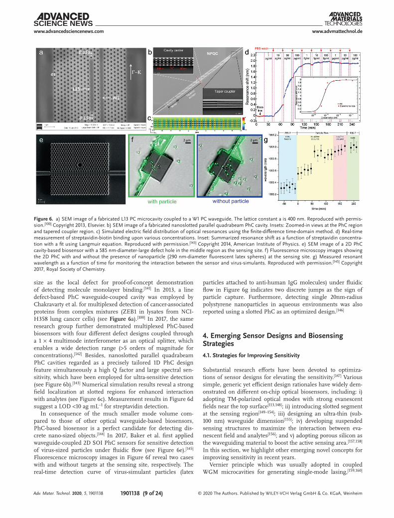
size as the local defect for proof-of-concept demonstration of detecting molecule monolayer binding.[141] In 2013, a line defect-based PhC waveguide-couped cavity was employed by Chakravarty et al. for multiplexed detection of cancer-associated proteins from complex mixtures (ZEB1 in lysates from NCI-H358 lung cancer cells) (see Figure 6a).[100] In 2017, the same research group further demonstrated multiplexed PhC-based biosensors with four different defect designs coupled through a 1 × 4 multimode interferometer as an optical splitter, which enables a wide detection range (>5 orders of magnitude for concentrations).[142] Besides, nanoslotted parallel quadrabeam PhC cavities regarded as a precisely tailored 1D PhC design feature simultaneously a high Q factor and large spectral sen-sitivity, which have been employed for ultra-sensitive detection (see Figure 6b).[143] Numerical simulation results reveal a strong field localization at slotted regions for enhanced interaction with analytes (see Figure 6c). Measurement results in Figure 6d suggest a LOD <10 ag mL−1 for streptavidin detection.
In consequence of the much smaller mode volume com-pared to those of other optical waveguide-based biosensors, PhC-based biosensor is a perfect candidate for detecting dis-crete nano-sized objects.[144] In 2017, Baker et al. first applied waveguide-coupled 2D SOI PhC sensors for sensitive detection of virus-sized particles under fluidic flow (see Figure 6e).[145] Fluorescence microscopy images in Figure 6f reveal two cases with and without targets at the sensing site, respectively. The real-time detection curve of virus-simulant particles (latex
particles attached to anti-human IgG molecules) under fluidic flow in Figure 6g indicates two discrete jumps as the sign of particle capture. Furthermore, detecting single 20nm-radius polystyrene nanoparticles in aqueous environments was also reported using a slotted PhC as an optimized design.[146]
4. Emerging Sensor Designs and Biosensing Strategies4.1. Strategies for Improving Sensitivity
Substantial research efforts have been devoted to optimiza-tions of sensor designs for elevating the sensitivity.[147] Various simple, generic yet efficient design rationales have widely dem-onstrated on different on-chip optical biosensors, including: i) adopting TM-polarized optical modes with strong evanescent fields near the top surface[113,148]; ii) introducing slotted segment at the sensing region[149–154]; iii) designing an ultra-thin (sub-100 nm) waveguide dimension[155]; iv) developing suspended sensing structures to maximize the interaction between eva-nescent field and analytes[156]; and v) adopting porous silicon as the waveguiding material to boost the active sensing area.[157,158] In this section, we highlight other emerging novel concepts for improving sensitivity in recent years.
Vernier principle which was usually adopted in coupled WGM microcavities for generating single-mode lasing,[159,160]
Adv. Mater. Technol. 2020, 5, 1901138
Figure 6. a) SEM image of a fabricated L13 PC microcavity coupled to a W1 PC waveguide. The lattice constant a is 400 nm. Reproduced with permis-sion.[100] Copyright 2013, Elsevier. b) SEM image of a fabricated nanoslotted parallel quadrabeam PhC cavity. Insets: Zoomed-in views at the PhC region and tapered coupler region. c) Simulated electric field distribution of optical resonances using the finite-difference time-domain method. d) Real-time measurement of streptavidin-biotin binding upon various concentrations. Inset: Summarized resonance shift as a function of streptavidin concentra-tion with a fit using Langmuir equation. Reproduced with permission.[143] Copyright 2014, American Institute of Physics. e) SEM image of a 2D PhC cavity-based biosensor with a 585 nm-diameter-large defect hole in the middle region as the sensing site. f) Fluorescence microscopy images showing the 2D PhC with and without the presence of nanoparticle (290 nm-diameter fluorescent latex spheres) at the sensing site. g) Measured resonant wavelength as a function of time for monitoring the interaction between the sensor and virus-simulants. Reproduced with permission.[145] Copyright 2017, Royal Society of Chemistry.
www.advancedsciencenews.com www.advmattechnol.de
1901138 (10 of 24) © 2020 The Authors. Published by WILEY-VCH Verlag GmbH & Co. KGaA, Weinheim
has also been proved as an efficient sensing scheme using cas-caded microrings.[161] The two microrings exhibit slightly dif-ferent sizes and hence mismatched free spectral ranges, which leads to a periodic envelope function with a peak corresponding to the maximum overlap of individual resonances. A tiny per-turbation of one microring is revealed as a giant shift of the main peak in the envelope. Such a data interrogation suggests a tremendous enhancement of sensitivity up to two orders of magnitude.[162–164] However, this method requires wavelength scanning over a very broad range, which largely limits the detection speed.
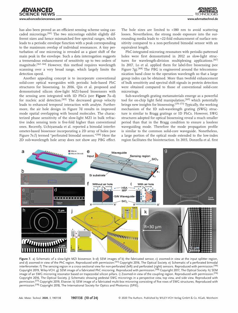
Another appealing concept is to incorporate conventional solid-core optical waveguides with periodic hole-based PhC structures for biosensing. In 2016, Qin et al. proposed and demonstrated silicon slow-light MZI-based biosensors with the sensing arm integrated with 1D PhCs (see Figure 7a–d) for nucleic acid detection.[165] The decreased group velocity leads to enhanced temporal interaction with analyte. Further-more, the air hole design in Figure 7d results in improved mode spatial overlapping with bound molecules. The charac-terized phase sensitivity of the slow-light MZI in bulk refrac-tive index sensing tests is five-fold higher than conventional ones. Recently, Uchiyamada et al. reported a bimodal interfer-ometer-based biosensor incorporating a 2D array of holes (see Figure 7e,f) termed “perforated bimodal sensors.”[166] Here the 2D sub-wavelength hole array does not show any PBG effect.
The hole sizes are limited to <180 nm to avoid scattering losses. Nevertheless, the strong mode exposure into the sur-rounding media leads to ≈22-fold enhancement of surface sen-sitivity compared to a non-perforated bimodal sensor with an equivalent length.
PhC-integrated microring resonators with periodic-patterned holes were first demonstrated in 2012 as slow-light struc-tures for wavelength-division multiplexing applications.[167] In 2017, Lo et al. applied them for label-free biosensing (see Figure 7g).[168] The PBG is engineered around the telecommu-nication band close to the operation wavelength so that a large group index can be obtained. More than twofold enhancement of bulk sensitivity and spectral shift signals in protein detection were obtained compared to those of conventional solid-core microrings.
Sub-wavelength grating metamaterials emerge as a powerful tool for on-chip light field manipulation,[169] which potentially brings new insights for biosensing.[170–173] Typically, the working mechanism of the 1D sub-wavelength grating (SWG) struc-ture is similar to Bragg gratings or 1D PhCs. However, SWG structures adopted for optical biosensing reveal a much smaller period than that in the Bragg condition to ensure a lossless waveguiding mode. Therefore the mode propagation profile is similar to the common solid-core waveguide. Nonetheless, a large portion of the optical mode extended to the low-index region facilitates the biointeraction. In 2015, Donzella et al. first
Adv. Mater. Technol. 2020, 5, 1901138
Figure 7. a) Schematic of a slow-light MZI biosensor. b–d) SEM images of b) the fabricated sensor, c) zoomed-in view at the input splitter region, and d) zoomed-in view of the PhC region. Reproduced with permission.[165] Copyright 2016, The Optical Society. e) Schematic of a perforated bimodal interferometer. f) The sensing region in a cross-sectional view for non-perforated (left) and perforated (right) sensors. Reproduced with permission.[166] Copyright 2019, Wiley-VCH. g) SEM image of a fabricated PhC microring. Reproduced with permission.[168] Copyright 2017, The Optical Society. h) SEM image of an SWG microring resonator based on trapezoidal silicon pillars. i) Zoomed-in view of the coupling region. Reproduced with permission.[176] Copyright 2016, The Optical Society. j) Schematic showing pedestal SWG microrings in a perspective view, top view, and side view. Reproduced with permission.[177] Copyright 2019, Elsevier. k) SEM image of a fabricated multi-box microring consisting of five rows of SWG structures. Reproduced with permission.[178] Copyright 2018, The International Society for Optics and Photonics (SPIE).
www.advancedsciencenews.com www.advmattechnol.de
1901138 (11 of 24) © 2020 The Authors. Published by WILEY-VCH Verlag GmbH & Co. KGaA, Weinheim
reported SWG microring with a characterized sensitivity to bulk refractive index change of ≈400 nm per refractive index unit (RIU) which is one order higher than that of common strip waveguide-based microring.[171] Then the SWG microring bio-sensors were exploited for label-free bio-sandwich assay.[174,175] In 2016, trapezoidal silicon pillar-based SWG microring (see Figure 7h,i) has been reported with mitigated bending losses and ≈3-5 fold enhancement of Q factor,[176] which is envisaged to further improve the sensing performance. In 2019, Chang et al. reported silicon pedestal SWG microrings as ultra-sensi-tive biosensors (see Figure 7j).[177] The pedestal structure formed by a controlled undercut etching maximizes the mode overlap-ping with surrounding media. The streptavidin-based bioassay suggests a ≈4-fold enhancement of spectral shift signals com-pared to that of the control SWG device.
In 2018, Luan et al. proposed and demonstrated a “multi-box” microring biosensor as a fusion of SWG and slot structures (see Figure 7k) with one of the characterized record highest sen-sitivities to bulk refractive index change of ≈580 nm per RIU and surface sensitivity of ≈1900 pm nm−1 in a standard bio-sandwich assay.[178,179] Very recently, the concept of “multi-box” waveguide has been further investigated with the incorporation of Bragg grating[180] and MZI-based[181] sensing structures.
4.2. Strategies for Simplifying the Biosensing Schemes
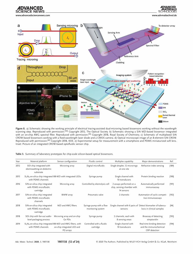
One key driving force behind the development of on-chip label-free optical biosensors is to minimize the demand for bulky and expensive instruments (e.g., high-precision wave-length-tunable lasers or off-chip spectrometers). In 2011, Claes et al. developed an on-chip wavelength interrogation scheme, which splits the transmission signals into multiple wavelength channels.[182] Adopting Vernier-cascade microrings as trans-ducers and compact arrayed waveguide grating (AWG) for on-chip spectrum analysis, this scheme only requires a broad-band light source and an IR camera for monitoring the output intensity signal in parallel. Later Song et al. reported a similar biosensing scheme working with a broadband light source,[183] as shown in Figure 8a. Here the optical resonance shift in the sensing ring is traced by electrical tuning of the reference ring. Therefore only a compact, cost-effective powermeter working in the IR wavelength is required. In 2018, Moock et al. reported a similar electrical tracing-based sensing concept for serially cascaded ring resonator arrays in the fashion of time-division multiplex.[184] Relying on a low-cost fixed wavelength laser source at the telecommunication band, the read-out rate can be improved from sub-Hz in conventional tunable laser-based schemes (limited by the scanning speed) to 100 Hz.[184] How-ever, only refractive index sensing for droplets was testified whereas label-free biodetection has not been reported.
Nevertheless, the SOI material platform and telecommuni-cation wavelength for biosensing are not the best choices for cost-effective biosensors because the camera or light source in IR wavelengths are still relatively expensive and not ubiquitous. Compared to silicon, SiN featuring a transparency window in shorter wavelengths (<1.1 µm) is highly sought for a miniatur-ized low-cost system utilizing widely available light sources such as LEDs, laser diodes and CMOS cameras. Recently,
Martens et al. developed a SiN MZI-based biosensing system working in the wavelength around 850 nm using a superlumi-nescent diode,[94] which is compatible with the response range of CMOS cameras. As illustrated in Figure 8b, the signal is filtered by AWG into 30 channels so that the spectrum can be reconstructed from the discretized data by fitting. Hence the spectral shift of interferometer signal can be traced in real-time.
Since 2014, Wang et al. have been developing multi-element cascaded microrings, also termed “coupled-resonator optical-waveguide (CROW)” as a biosensor using elastic light scat-tering-based pattern recognition technique (see Figure 8c,d).[185] The calibrated sensing system only requires a fixed-wavelength laser diode and a CMOS camera.[186] In the latest demonstra-tions of streptavidin detection using surface-functionalized CROWs, the varying light scattering patterns are recorded and analyzed through a correlation algorithm so that the relative spectral shift can be readily extracted.[85,187] In this scheme, an on-chip spectrometer such as an AWG is circumvented, which largely minimizes the sensor footprint and facilitates multi-plexed detection on a single chip. As presented in Figure 8e, the miniaturized optofluidic integrated CROW biosensor chip can work with a smartphone camera through a PDMS soft lens as the optical interface, which paves the way toward POC applications.
5. Laboratory Prototypes toward POC Applications
In recent years, various developed laboratory prototypes further approach the envisaged goal of miniaturized and multi-func-tional lab-on-a-chip optical bioanalytical systems.[188] Integrating a biosensor chip with advanced microfluidic processing units and optoelectronic components render the technology closer to commercialization. Table 3 summarizes the state-of-the-art laboratory prototypes with integrated microfluidic modules or optoelectronic components.
5.1. Laboratory Prototypes with Advanced Microfluidic Integration
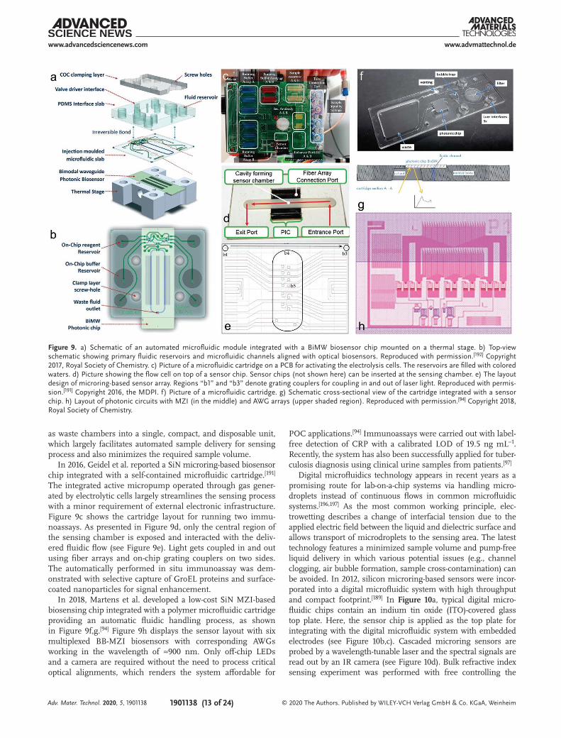
In 2017, Szydzik et al. reported a multiplexed BiMW-based bio-sensor chip integrated with pneumatic valve-based microfluidic modules offering a high degree of flexible, automatic and on-chip sequential manipulation of multiple fluidic samples.[192] As illustrated in Figure 9a,b, utilizing a one-step injection molding technique, a thin PDMS slab-based microfluidic channel was integrated with the silicon sensor chip and also a thick PDMS interface slab. An automatic competitive immunoassay was performed with “cycles” of reference and competitive assays for detecting tetracycline antibiotics.
Apart from developing sophisticated microfluidic circuits on top of the sensor chip, it is highly desirable to utilize low-cost polymer microfluidic cartridges made by injection molding with mass production where the chip-scale label-free optical biosen-sors serve as the inserted and replaceable element. Nowadays, cartridge-based microfluidics emerges as a promising tech-nology for in vitro diagnostics.[195] Typical microfluidic cartridge integrates storage, handing of fluidic samples or reagents as well
Adv. Mater. Technol. 2020, 5, 1901138
www.advancedsciencenews.com www.advmattechnol.de
1901138 (12 of 24) © 2020 The Authors. Published by WILEY-VCH Verlag GmbH & Co. KGaA, WeinheimAdv. Mater. Technol. 2020, 5, 1901138
Table 3. Summary of laboratory prototypes for chip-scale silicon-based optical biosensors.
Year Material platform Sensor configuration Fluidic control Multiplex capability Major demonstrations Ref.
2012 SOI chip integrated with electrowetting-on-dielectric
substrate
Microring array Digital microfluidic Single droplet, 12 microrings at one site
Refractive index sensing [189]
2015 Si3N4-on-silica chip integrated with PDMS channels
BB-MZI with integrated LEDs Syringe pump Single channel with 10 transducers
Protein binding reaction [190]
2016 SiN-on-silica chip integrated with PDMS microfluidic
cartridge
Microring array Controlled by electrolysis cell 2 assays performed on a chip, sensing chamber with
14 sensors
Automatically performed immunoassay
[191]
2017 SiN-on-silica chip integrated with PDMS microfluidic
channels
BiMW array Pneumatic valve 2 channels Automation of cyclic competi-tive immunoassays
[192]
2018 SiN-on-silica chip integrated with PDMS microfluidic
cartridge
MZI and AWG filters Syringe pump with a flow monitoring system
Single channel with 6 pairs of sensors
Detect biomarker of tubercu-losis in clinical samples
[94]
2018 SOI chip with fan-out wafer-level-packaging process
Microring array and on-chip Ge PDs
Syringe pump 2 channels, each with 8 sensing areas
Bioassay of detecting streptavidin
[193]
2019 Si3N4-on-silica chip integrated with PDMS channels
BB-MZI and AWG filters, with on-chip integrated LED and
PD arrays
Controlled with a fluidic cartridge
Single channel with 10 transducers
Real-time binding detection and the immunochemical
CRP detection
[194]
Figure 8. a) Schematic showing the working principle of electrical tracing-assisted dual-microring based biosensors working without the wavelength scanning step. Reproduced with permission.[183] Copyright 2012, The Optical Society. b) Schematic showing a SiN MZI-based biosensor integrated with an on-chip AWG spectral filter. Reproduced with permission.[94] Copyright 2018, Royal Society of Chemistry. c) Schematic of multiplexed SiN CROW-based biosensors working with a fixed-wavelength laser diode and a CMOS camera. d) Optical microscope image of an 8-element SiN CROW. Reproduced with permission.[85] Copyright 2018, IEEE. e) Experimental setup for measurement with a smartphone and PDMS miniaturized soft lens. Inset: Picture of an integrated CROW-based optofluidic sensor chip.
www.advancedsciencenews.com www.advmattechnol.de
1901138 (13 of 24) © 2020 The Authors. Published by WILEY-VCH Verlag GmbH & Co. KGaA, Weinheim
as waste chambers into a single, compact, and disposable unit, which largely facilitates automated sample delivery for sensing process and also minimizes the required sample volume.
In 2016, Geidel et al. reported a SiN microring-based biosensor chip integrated with a self-contained microfluidic cartridge.[191] The integrated active micropump operated through gas gener-ated by electrolytic cells largely streamlines the sensing process with a minor requirement of external electronic infrastructure. Figure 9c shows the cartridge layout for running two immu-noassays. As presented in Figure 9d, only the central region of the sensing chamber is exposed and interacted with the deliv-ered fluidic flow (see Figure 9e). Light gets coupled in and out using fiber arrays and on-chip grating couplers on two sides. The automatically performed in situ immunoassay was dem-onstrated with selective capture of GroEL proteins and surface-coated nanoparticles for signal enhancement.
In 2018, Martens et al. developed a low-cost SiN MZI-based biosensing chip integrated with a polymer microfluidic cartridge providing an automatic fluidic handling process, as shown in Figure 9f,g.[94] Figure 9h displays the sensor layout with six multiplexed BB-MZI biosensors with corresponding AWGs working in the wavelength of ≈900 nm. Only off-chip LEDs and a camera are required without the need to process critical optical alignments, which renders the system affordable for
POC applications.[94] Immunoassays were carried out with label-free detection of CRP with a calibrated LOD of 19.5 ng mL−1. Recently, the system has also been successfully applied for tuber-culosis diagnosis using clinical urine samples from patients.[97]
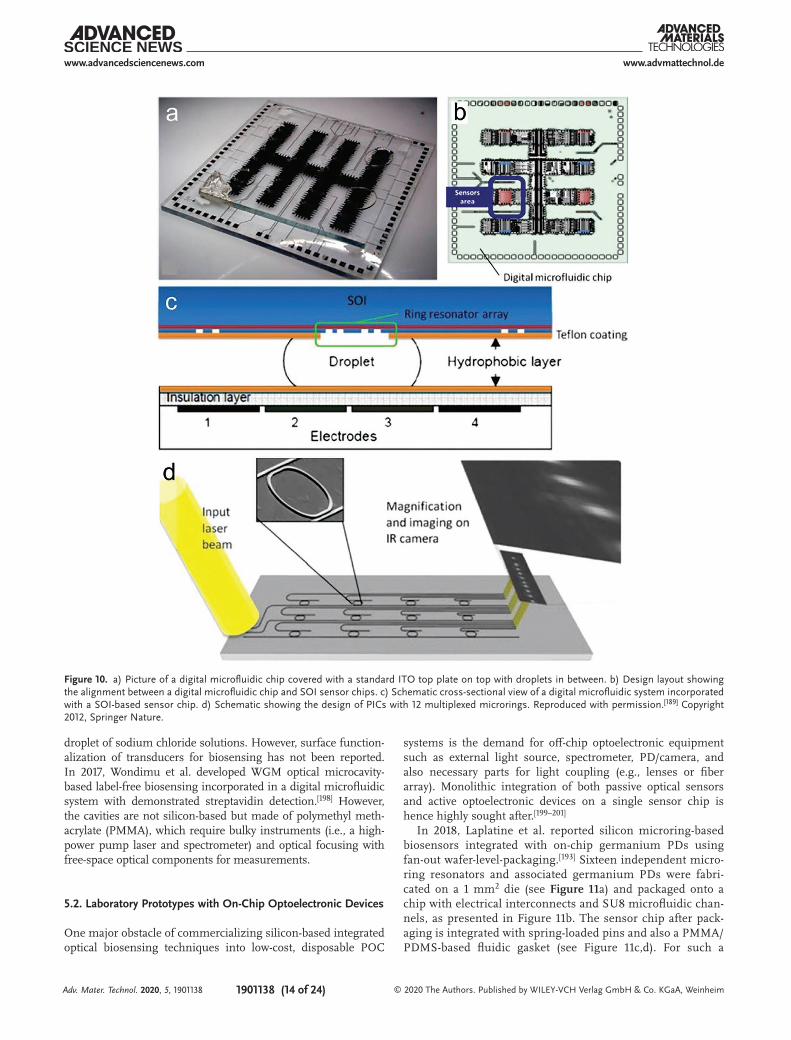
Digital microfluidics technology appears in recent years as a promising route for lab-on-a-chip systems via handling micro-droplets instead of continuous flows in common microfluidic systems.[196,197] As the most common working principle, elec-trowetting describes a change of interfacial tension due to the applied electric field between the liquid and dielectric surface and allows transport of microdroplets to the sensing area. The latest technology features a minimized sample volume and pump-free liquid delivery in which various potential issues (e.g., channel clogging, air bubble formation, sample cross-contamination) can be avoided. In 2012, silicon microring-based sensors were incor-porated into a digital microfluidic system with high throughput and compact footprint.[189] In Figure 10a, typical digital micro-fluidic chips contain an indium tin oxide (ITO)-covered glass top plate. Here, the sensor chip is applied as the top plate for integrating with the digital microfluidic system with embedded electrodes (see Figure 10b,c). Cascaded microring sensors are probed by a wavelength-tunable laser and the spectral signals are read out by an IR camera (see Figure 10d). Bulk refractive index sensing experiment was performed with free controlling the
Adv. Mater. Technol. 2020, 5, 1901138
Figure 9. a) Schematic of an automated microfluidic module integrated with a BiMW biosensor chip mounted on a thermal stage. b) Top-view schematic showing primary fluidic reservoirs and microfluidic channels aligned with optical biosensors. Reproduced with permission.[192] Copyright 2017, Royal Society of Chemistry. c) Picture of a microfluidic cartridge on a PCB for activating the electrolysis cells. The reservoirs are filled with colored waters. d) Picture showing the flow cell on top of a sensor chip. Sensor chips (not shown here) can be inserted at the sensing chamber. e) The layout design of microring-based sensor array. Regions “b1” and “b3” denote grating couplers for coupling in and out of laser light. Reproduced with permis-sion.[191] Copyright 2016, the MDPI. f) Picture of a microfluidic cartridge. g) Schematic cross-sectional view of the cartridge integrated with a sensor chip. h) Layout of photonic circuits with MZI (in the middle) and AWG arrays (upper shaded region). Reproduced with permission.[94] Copyright 2018, Royal Society of Chemistry.
www.advancedsciencenews.com www.advmattechnol.de
1901138 (14 of 24) © 2020 The Authors. Published by WILEY-VCH Verlag GmbH & Co. KGaA, Weinheim
droplet of sodium chloride solutions. However, surface function-alization of transducers for biosensing has not been reported. In 2017, Wondimu et al. developed WGM optical microcavity-based label-free biosensing incorporated in a digital microfluidic system with demonstrated streptavidin detection.[198] However, the cavities are not silicon-based but made of polymethyl meth-acrylate (PMMA), which require bulky instruments (i.e., a high-power pump laser and spectrometer) and optical focusing with free-space optical components for measurements.
5.2. Laboratory Prototypes with On-Chip Optoelectronic Devices
One major obstacle of commercializing silicon-based integrated optical biosensing techniques into low-cost, disposable POC
systems is the demand for off-chip optoelectronic equipment such as external light source, spectrometer, PD/camera, and also necessary parts for light coupling (e.g., lenses or fiber array). Monolithic integration of both passive optical sensors and active optoelectronic devices on a single sensor chip is hence highly sought after.[199–201]
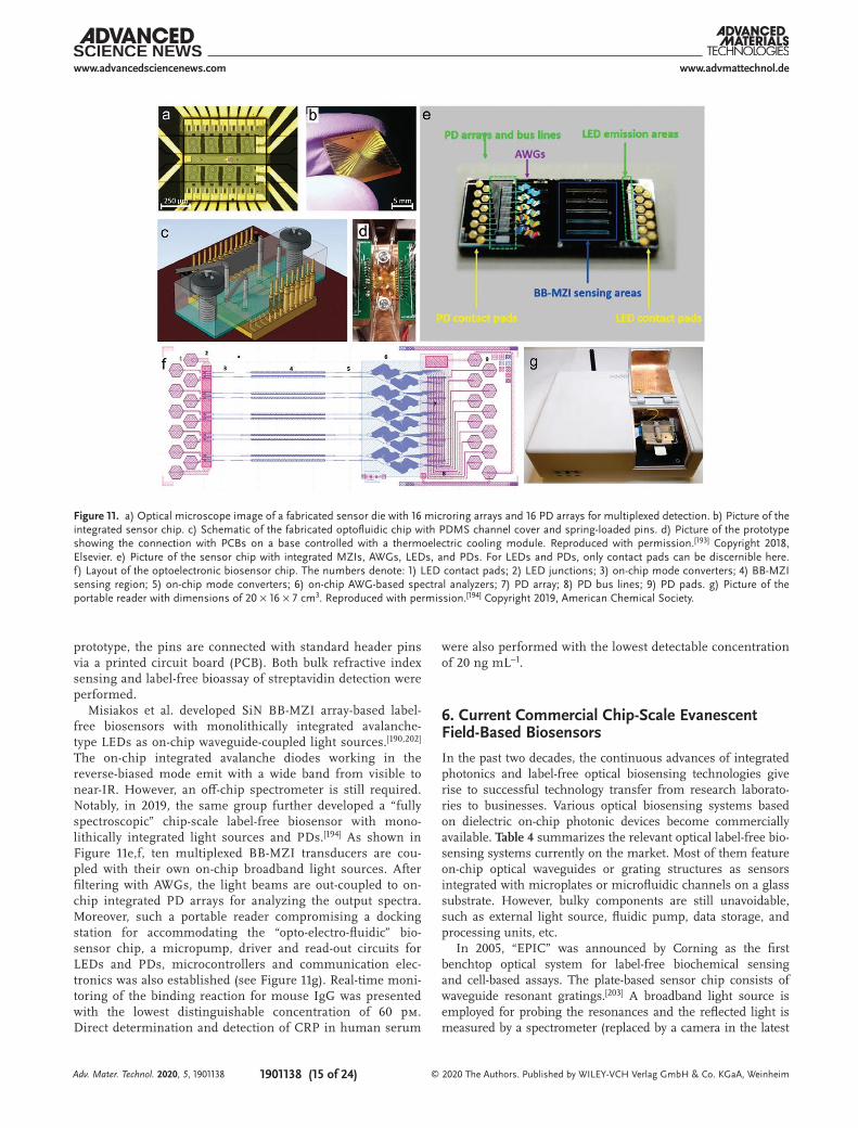
In 2018, Laplatine et al. reported silicon microring-based biosensors integrated with on-chip germanium PDs using fan-out wafer-level-packaging.[193] Sixteen independent micro-ring resonators and associated germanium PDs were fabri-cated on a 1 mm2 die (see Figure 11a) and packaged onto a chip with electrical interconnects and SU8 microfluidic chan-nels, as presented in Figure 11b. The sensor chip after pack-aging is integrated with spring-loaded pins and also a PMMA/PDMS-based fluidic gasket (see Figure 11c,d). For such a
Adv. Mater. Technol. 2020, 5, 1901138
Figure 10. a) Picture of a digital microfluidic chip covered with a standard ITO top plate on top with droplets in between. b) Design layout showing the alignment between a digital microfluidic chip and SOI sensor chips. c) Schematic cross-sectional view of a digital microfluidic system incorporated with a SOI-based sensor chip. d) Schematic showing the design of PICs with 12 multiplexed microrings. Reproduced with permission.[189] Copyright 2012, Springer Nature.
www.advancedsciencenews.com www.advmattechnol.de
1901138 (15 of 24) © 2020 The Authors. Published by WILEY-VCH Verlag GmbH & Co. KGaA, Weinheim
prototype, the pins are connected with standard header pins via a printed circuit board (PCB). Both bulk refractive index sensing and label-free bioassay of streptavidin detection were performed.
Misiakos et al. developed SiN BB-MZI array-based label-free biosensors with monolithically integrated avalanche-type LEDs as on-chip waveguide-coupled light sources.[190,202] The on-chip integrated avalanche diodes working in the reverse-biased mode emit with a wide band from visible to near-IR. However, an off-chip spectrometer is still required. Notably, in 2019, the same group further developed a “fully spectroscopic” chip-scale label-free biosensor with mono-lithically integrated light sources and PDs.[194] As shown in Figure 11e,f, ten multiplexed BB-MZI transducers are cou-pled with their own on-chip broadband light sources. After filtering with AWGs, the light beams are out-coupled to on-chip integrated PD arrays for analyzing the output spectra. Moreover, such a portable reader compromising a docking station for accommodating the “opto-electro-fluidic” bio-sensor chip, a micropump, driver and read-out circuits for LEDs and PDs, microcontrollers and communication elec-tronics was also established (see Figure 11g). Real-time moni-toring of the binding reaction for mouse IgG was presented with the lowest distinguishable concentration of 60 pm. Direct determination and detection of CRP in human serum
were also performed with the lowest detectable concentration of 20 ng mL−1.
6. Current Commercial Chip-Scale Evanescent Field-Based BiosensorsIn the past two decades, the continuous advances of integrated photonics and label-free optical biosensing technologies give rise to successful technology transfer from research laborato-ries to businesses. Various optical biosensing systems based on dielectric on-chip photonic devices become commercially available. Table 4 summarizes the relevant optical label-free bio-sensing systems currently on the market. Most of them feature on-chip optical waveguides or grating structures as sensors integrated with microplates or microfluidic channels on a glass substrate. However, bulky components are still unavoidable, such as external light source, fluidic pump, data storage, and processing units, etc.
In 2005, “EPIC” was announced by Corning as the first benchtop optical system for label-free biochemical sensing and cell-based assays. The plate-based sensor chip consists of waveguide resonant gratings.[203] A broadband light source is employed for probing the resonances and the reflected light is measured by a spectrometer (replaced by a camera in the latest
Adv. Mater. Technol. 2020, 5, 1901138
Figure 11. a) Optical microscope image of a fabricated sensor die with 16 microring arrays and 16 PD arrays for multiplexed detection. b) Picture of the integrated sensor chip. c) Schematic of the fabricated optofluidic chip with PDMS channel cover and spring-loaded pins. d) Picture of the prototype showing the connection with PCBs on a base controlled with a thermoelectric cooling module. Reproduced with permission.[193] Copyright 2018, Elsevier. e) Picture of the sensor chip with integrated MZIs, AWGs, LEDs, and PDs. For LEDs and PDs, only contact pads can be discernible here. f) Layout of the optoelectronic biosensor chip. The numbers denote: 1) LED contact pads; 2) LED junctions; 3) on-chip mode converters; 4) BB-MZI sensing region; 5) on-chip mode converters; 6) on-chip AWG-based spectral analyzers; 7) PD array; 8) PD bus lines; 9) PD pads. g) Picture of the portable reader with dimensions of 20 × 16 × 7 cm3. Reproduced with permission.[194] Copyright 2019, American Chemical Society.
www.advancedsciencenews.com www.advmattechnol.de
1901138 (16 of 24) © 2020 The Authors. Published by WILEY-VCH Verlag GmbH & Co. KGaA, Weinheim
models). Likewise, the “ResoSens” system developed by Reso-nant Sensors makes use of a similar grating structure based on TiO2 substrate for label-free bioassays. Afterward, a biosensing system featuring “optical waveguide lightmode spectroscopy (OWLS)” technique was developed by Microvacuum. The sensor structure combines a grating coupler and optical waveguide.[204] A linearly polarized red laser light is coupled into the grating coupler with an optimized incidence angle and then guided by TIR to the output port where it is detected by a PD. The whole system is integrated on a precision goniometer so that any per-turbation on the sensor surface can be extracted by monitoring the variation of incidence angle.
In 2014, “Creoptix WAVE” was launched as a new label-free test bench with 4-channel real-time measurements. The grating-coupled interferometry (GCI) technique involves optical waveguides with two input coupling and one output coupling gratings, suggesting clear advantages compared to the tradi-tional grating coupler-based biosensors.[205,206] Owing to the waveguide-based interferometry, the analyte information is extracted through a time-dependent and robust phase shift signal. Thus the noise from temperature shifts or mechanical distortions can be largely mitigated compared to the traditional scheme of detecting interference signals at the far-field. While the product is based on the Ta2O5-on-glass material platform, researchers have also demonstrated the GCI technique on the silicon platform in research laboratories.[207]
Genalyte has been developing the “Maverick” detection system based on the latest silicon photonics technology over the past decade. The disposable and consumable sensing chip contains two fluidic channels and each channel covers 16 waveguide-coupled microring-based sensing units.[208] Single test against 16 analytes can be performed with a low sample consumption down to 5–10 µL in only 10 min. In particular, the system performs biomolecule assays in multiple com-plex matrices such as serum, plasma, whole blood, and crude extracts, which largely simplifies the sample preparation step. Besides, quantitative mass concentration detection has been reported for industrial polymer using the Maverick system.[209] The extracted “polydispersity index” is in a good agreement with standard methods (e.g., differential refractive index detec-tors and UV chromatogram). Very recently, the system has been employed on clinically diagnosed patients for 12 assays of
simultaneously detecting autoantibodies in whole blood within less than 15 min, suggesting clear advantages over standard clinical tests.[210]
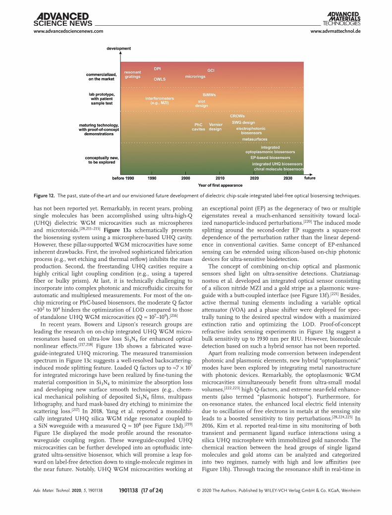
7. The Roadmap for Future Silicon-Based Optical BiosensorsFigure 12 presents an overview of technology developments on on-chip integrated dielectric photonic devices for label-free biosensing. Basic building blocks in silicon photonics, such as slab waveguides, straight ridge waveguides, multimode waveguides, and resonant gratings were exploited for optical biosensing at early stages. Then functional photonic devices originally for on-chip optical signal processing in communica-tions and interconnects such as microrings and interferometers were also employed for biosensing. Many of these techniques have been successfully commercialized as bioanalytical sys-tems on the market while others are under tests with clinical samples of patients for in vitro medical diagnostics. In the past decade, advanced sensor designs and alternative sensing mechanisms appear, such as those with multiple cross-coupled units (e.g., cascaded rings with Vernier effect, CROWs), or fine engineered sub-wavelength structures for either light localiza-tion (e.g., PhCs, metasurfaces) or lossless propagation with a large mode overlapping to the analytes (e.g., SWG structure). These relatively new techniques are still attracting extensive research investigations from research groups over the world. Regarding the future development, various new findings and fresh concepts in optical physics may point the way for next-generation silicon-based on-chip biosensors to unprecedented sensing performance in terms of sensitivity, LOD, time resolu-tion, specificity, stability, etc.
7.1. Toward Ultra-Sensitive Biodetection Systems
Detecting single biological entities is always a crucial topic in fundamental science.[25,28] Although plenty of strategies have been explored toward ultra-sensitive detection, the typical LOD of current silicon-based planar optical biosensors are mostly ∼ fM to nM. To our knowledge, single-molecule detection
Adv. Mater. Technol. 2020, 5, 1901138
Table 4. List of currently commercialized label-free biosensing systems on the market based on dielectric photonic chips.
Instrument (Company) Material platform Core technology Fluidic condition Multiplex capability Main functionalities
EPIC system (Corning) Glass Resonant waveguide gratings
Plate-based 384 well plate Detection of enzyme, small molecule, protein and DNA;
antibody and cell-based studies
ResoSens system (ResonantSensors)
TiO2 Resonant waveguide gratings
Plate-based 96 or 384 well plate Cell-based assays and antibody–antigen interactions
OWLS system (Microvacuum)
SixTi(1−x)O2 on glass Optical waveguide and grating couplers
Flow [0.1 µL min−1 –30 mL min−1]
Single measurement Protein adsorption; antigen anti-body binding; drug screening,
binding kinetics; immunosensing
Creoptix WAVE system (Creoptix AG)
Ta2O5 on glass Grating-coupled interferometry
Flow [up to 400 µL min−1] 2 or 4 channels Small-molecule characterization; kinetic analysis; drug test
Maverick system (Genalyte) SOI Microring arrays Flow [up to 30 µL min−1] 2 channels, 16 analytes per channel
Protein binding events, mass concentration detection, etc.
www.advancedsciencenews.com www.advmattechnol.de
1901138 (17 of 24) © 2020 The Authors. Published by WILEY-VCH Verlag GmbH & Co. KGaA, Weinheim
has not been reported yet. Remarkably, in recent years, probing single molecules has been accomplished using ultra-high-Q (UHQ) dielectric WGM microcavities such as microspheres and microtoroids.[28,211–215] Figure 13a schematically presents the biosensing system using a microsphere-based UHQ cavity. However, these pillar-supported WGM microcavities have some inherent drawbacks. First, the involved sophisticated fabrication process (e.g., wet etching and thermal reflow) inhibits the mass production. Second, the freestanding UHQ cavities require a highly critical light coupling condition (e.g., using a tapered fiber or bulky prism). At last, it is technically challenging to incorporate into complex photonic and microfluidic circuits for automatic and multiplexed measurements. For most of the on-chip microring or PhC-based biosensors, the moderate Q factor ≈102 to 104 hinders the optimization of LOD compared to those of standalone UHQ WGM microcavities (Q ≈ 107–109).[216]
In recent years, Bowers and Lipson’s research groups are leading the research on on-chip integrated UHQ WGM micro-resonators based on ultra-low loss Si3N4 for enhanced optical nonlinear effects.[217,218] Figure 13b shows a fabricated wave-guide-integrated UHQ microring. The measured transmission spectrum in Figure 13c suggests a well-resolved backscattering-induced mode splitting feature. Loaded Q factors up to ≈7 × 10⁷ for integrated microrings have been realized by fine-tuning the material composition in Si3N4 to minimize the absorption loss and developing new surface smooth techniques (e.g., chem-ical mechanical polishing of deposited Si3N4 films, multipass lithography, and hard mask-based dry etching) to minimize the scattering loss.[217] In 2018, Yang et al. reported a monolithi-cally integrated UHQ silica WGM ridge resonator coupled to a SiN waveguide with a measured Q ≈ 108 (see Figure 13d).[219] Figure 13e displayed the mode profile around the resonator-waveguide coupling region. These waveguide-coupled UHQ microcavities can be further developed into an optofluidic inte-grated ultra-sensitive biosensor, which will promise a leap for-ward on label-free detection down to single-molecule regimes in the near future. Notably, UHQ WGM microcavities working at
an exceptional point (EP) as the degeneracy of two or multiple eigenstates reveal a much-enhanced sensitivity toward local-ized nanoparticle-induced perturbations.[220] The induced mode splitting around the second-order EP suggests a square-root dependence of the perturbation rather than the linear depend-ence in conventional cavities. Same concept of EP-enhanced sensing can be extended using silicon-based on-chip photonic devices for ultra-sensitive biodetection.
The concept of combining on-chip optical and plasmonic sensors shed light on ultra-sensitive detections. Chatzianag-nostou et al. developed an integrated optical sensor consisting of a silicon nitride MZI and a gold stripe as a plasmonic wave-guide with a butt-coupled interface (see Figure 13f).[221] Besides, active thermal tuning elements including a variable optical attenuator (VOA) and a phase shifter were deployed for spec-trally tuning to the desired spectral window with a maximized extinction ratio and optimizing the LOD. Proof-of-concept refractive index sensing experiments in Figure 13g suggest a bulk sensitivity up to 1930 nm per RIU. However, biomolecule detection based on such a hybrid sensor has not been reported.
Apart from realizing mode conversion between independent photonic and plasmonic elements, new hybrid “optoplasmonic” modes have been explored by integrating metal nanostructure with photonic devices. Remarkably, the optoplasmonic WGM microcavities simultaneously benefit from ultra-small modal volumes,[222,223] high Q-factors, and extreme near-field enhance-ments (also termed “plasmonic hotspot”). Furthermore, for on-resonance states, the enhanced local electric field intensity due to oscillation of free electrons in metals at the sensing site leads to a boosted sensitivity to tiny perturbations.[28,224,225] In 2016, Kim et al. reported real-time in situ monitoring of both transient and permanent ligand surface interactions using a silica UHQ microsphere with immobilized gold nanorods. The chemical reaction between the head groups of single ligand molecules and gold atoms can be analyzed and categorized into two regimes, namely with high and low affinities (see Figure 13h). Through tracing the resonance shift in real-time in
Adv. Mater. Technol. 2020, 5, 1901138
Figure 12. The past, state-of-the-art and our envisioned future development of dielectric chip-scale integrated label-free optical biosensing techniques.
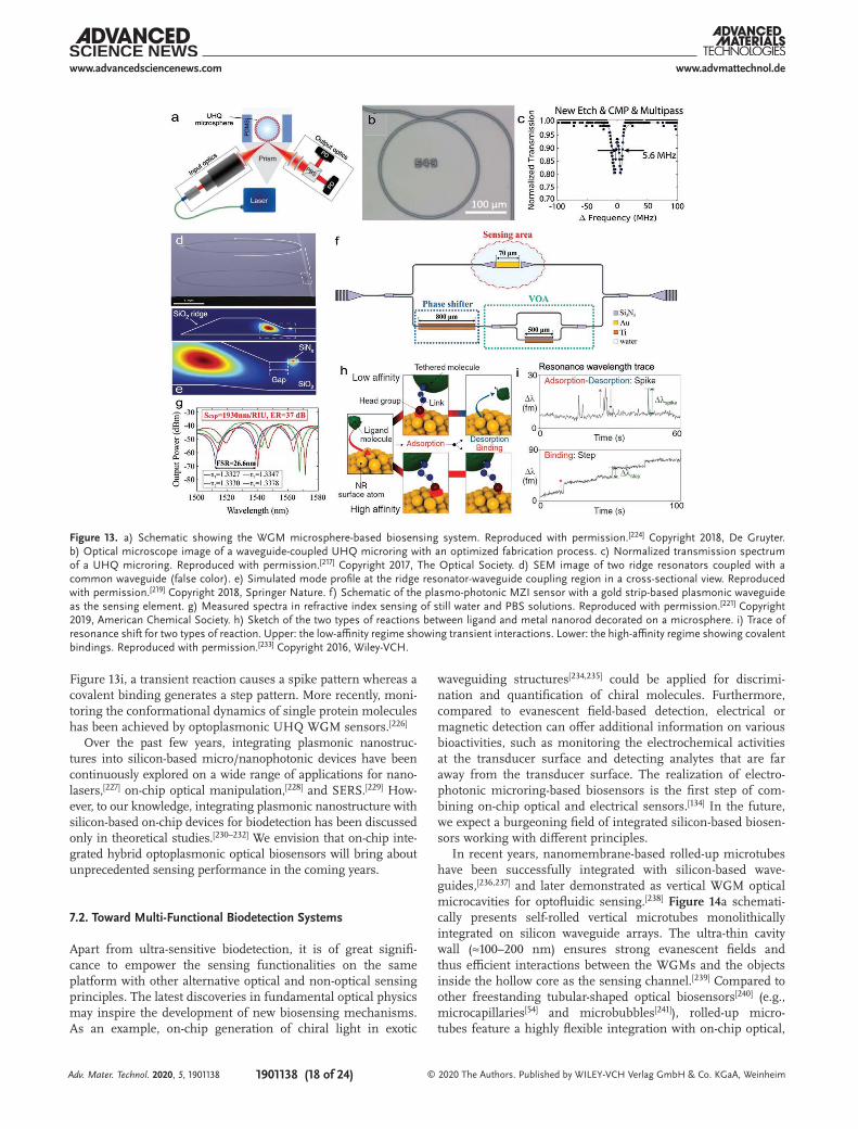
www.advancedsciencenews.com www.advmattechnol.de
1901138 (18 of 24) © 2020 The Authors. Published by WILEY-VCH Verlag GmbH & Co. KGaA, Weinheim
Figure 13i, a transient reaction causes a spike pattern whereas a covalent binding generates a step pattern. More recently, moni-toring the conformational dynamics of single protein molecules has been achieved by optoplasmonic UHQ WGM sensors.[226]
Over the past few years, integrating plasmonic nanostruc-tures into silicon-based micro/nanophotonic devices have been continuously explored on a wide range of applications for nano-lasers,[227] on-chip optical manipulation,[228] and SERS.[229] How-ever, to our knowledge, integrating plasmonic nanostructure with silicon-based on-chip devices for biodetection has been discussed only in theoretical studies.[230–232] We envision that on-chip inte-grated hybrid optoplasmonic optical biosensors will bring about unprecedented sensing performance in the coming years.
7.2. Toward Multi-Functional Biodetection Systems
Apart from ultra-sensitive biodetection, it is of great signifi-cance to empower the sensing functionalities on the same platform with other alternative optical and non-optical sensing principles. The latest discoveries in fundamental optical physics may inspire the development of new biosensing mechanisms. As an example, on-chip generation of chiral light in exotic
waveguiding structures[234,235] could be applied for discrimi-nation and quantification of chiral molecules. Furthermore, compared to evanescent field-based detection, electrical or magnetic detection can offer additional information on various bioactivities, such as monitoring the electrochemical activities at the transducer surface and detecting analytes that are far away from the transducer surface. The realization of electro-photonic microring-based biosensors is the first step of com-bining on-chip optical and electrical sensors.[134] In the future, we expect a burgeoning field of integrated silicon-based biosen-sors working with different principles.
In recent years, nanomembrane-based rolled-up microtubes have been successfully integrated with silicon-based wave-guides,[236,237] and later demonstrated as vertical WGM optical microcavities for optofluidic sensing.[238] Figure 14a schemati-cally presents self-rolled vertical microtubes monolithically integrated on silicon waveguide arrays. The ultra-thin cavity wall (≈100–200 nm) ensures strong evanescent fields and thus efficient interactions between the WGMs and the objects inside the hollow core as the sensing channel.[239] Compared to other freestanding tubular-shaped optical biosensors[240] (e.g., microcapillaries[54] and microbubbles[241]), rolled-up micro-tubes feature a highly flexible integration with on-chip optical,
Adv. Mater. Technol. 2020, 5, 1901138
Figure 13. a) Schematic showing the WGM microsphere-based biosensing system. Reproduced with permission.[224] Copyright 2018, De Gruyter. b) Optical microscope image of a waveguide-coupled UHQ microring with an optimized fabrication process. c) Normalized transmission spectrum of a UHQ microring. Reproduced with permission.[217] Copyright 2017, The Optical Society. d) SEM image of two ridge resonators coupled with a common waveguide (false color). e) Simulated mode profile at the ridge resonator-waveguide coupling region in a cross-sectional view. Reproduced with permission.[219] Copyright 2018, Springer Nature. f) Schematic of the plasmo-photonic MZI sensor with a gold strip-based plasmonic waveguide as the sensing element. g) Measured spectra in refractive index sensing of still water and PBS solutions. Reproduced with permission.[221] Copyright 2019, American Chemical Society. h) Sketch of the two types of reactions between ligand and metal nanorod decorated on a microsphere. i) Trace of resonance shift for two types of reaction. Upper: the low-affinity regime showing transient interactions. Lower: the high-affinity regime showing covalent bindings. Reproduced with permission.[233] Copyright 2016, Wiley-VCH.
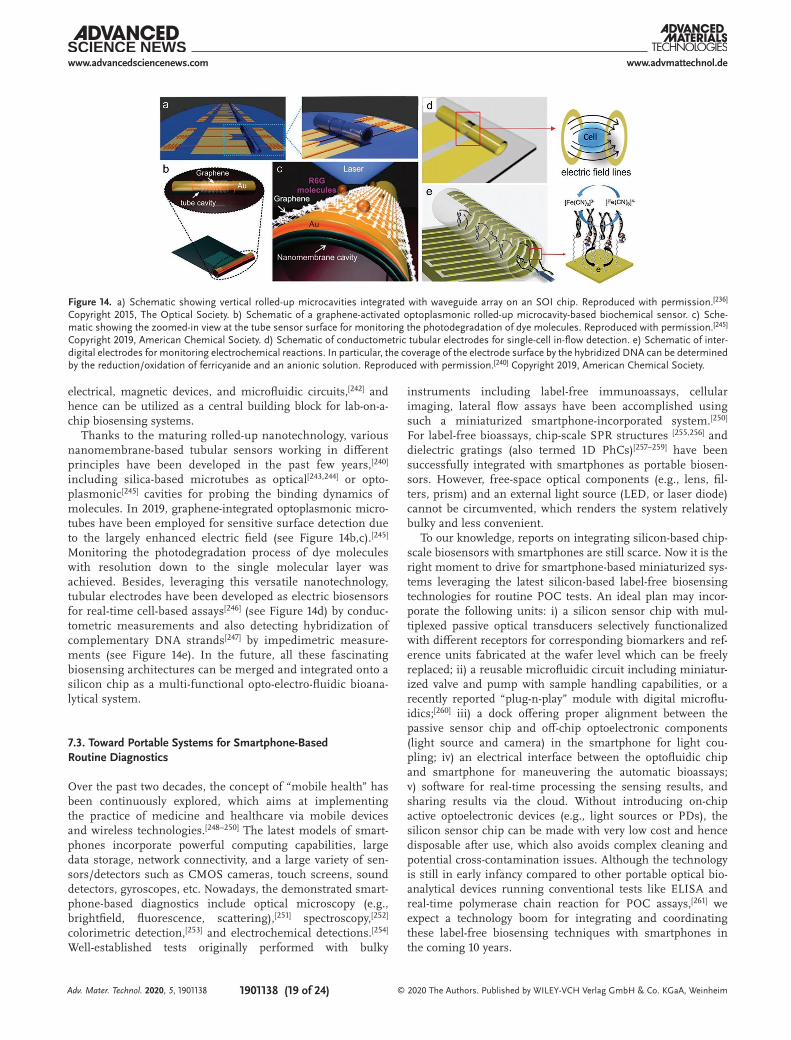
www.advancedsciencenews.com www.advmattechnol.de
1901138 (19 of 24) © 2020 The Authors. Published by WILEY-VCH Verlag GmbH & Co. KGaA, Weinheim
electrical, magnetic devices, and microfluidic circuits,[242] and hence can be utilized as a central building block for lab-on-a-chip biosensing systems.
Thanks to the maturing rolled-up nanotechnology, various nanomembrane-based tubular sensors working in different principles have been developed in the past few years,[240] including silica-based microtubes as optical[243,244] or opto-plasmonic[245] cavities for probing the binding dynamics of molecules. In 2019, graphene-integrated optoplasmonic micro-tubes have been employed for sensitive surface detection due to the largely enhanced electric field (see Figure 14b,c).[245] Monitoring the photodegradation process of dye molecules with resolution down to the single molecular layer was achieved. Besides, leveraging this versatile nanotechnology, tubular electrodes have been developed as electric biosensors for real-time cell-based assays[246] (see Figure 14d) by conduc-tometric measurements and also detecting hybridization of complementary DNA strands[247] by impedimetric measure-ments (see Figure 14e). In the future, all these fascinating biosensing architectures can be merged and integrated onto a silicon chip as a multi-functional opto-electro-fluidic bioana-lytical system.
7.3. Toward Portable Systems for Smartphone-Based Routine Diagnostics
Over the past two decades, the concept of “mobile health” has been continuously explored, which aims at implementing the practice of medicine and healthcare via mobile devices and wireless technologies.[248–250] The latest models of smart-phones incorporate powerful computing capabilities, large data storage, network connectivity, and a large variety of sen-sors/detectors such as CMOS cameras, touch screens, sound detectors, gyroscopes, etc. Nowadays, the demonstrated smart-phone-based diagnostics include optical microscopy (e.g., brightfield, fluorescence, scattering),[251] spectroscopy,[252] colorimetric detection,[253] and electrochemical detections.[254] Well-established tests originally performed with bulky
instruments including label-free immunoassays, cellular imaging, lateral flow assays have been accomplished using such a miniaturized smartphone-incorporated system.[250] For label-free bioassays, chip-scale SPR structures [255,256] and dielectric gratings (also termed 1D PhCs)[257–259] have been successfully integrated with smartphones as portable biosen-sors. However, free-space optical components (e.g., lens, fil-ters, prism) and an external light source (LED, or laser diode) cannot be circumvented, which renders the system relatively bulky and less convenient.
To our knowledge, reports on integrating silicon-based chip-scale biosensors with smartphones are still scarce. Now it is the right moment to drive for smartphone-based miniaturized sys-tems leveraging the latest silicon-based label-free biosensing technologies for routine POC tests. An ideal plan may incor-porate the following units: i) a silicon sensor chip with mul-tiplexed passive optical transducers selectively functionalized with different receptors for corresponding biomarkers and ref-erence units fabricated at the wafer level which can be freely replaced; ii) a reusable microfluidic circuit including miniatur-ized valve and pump with sample handling capabilities, or a recently reported “plug-n-play” module with digital microflu-idics;[260] iii) a dock offering proper alignment between the passive sensor chip and off-chip optoelectronic components (light source and camera) in the smartphone for light cou-pling; iv) an electrical interface between the optofluidic chip and smartphone for maneuvering the automatic bioassays; v) software for real-time processing the sensing results, and sharing results via the cloud. Without introducing on-chip active optoelectronic devices (e.g., light sources or PDs), the silicon sensor chip can be made with very low cost and hence disposable after use, which also avoids complex cleaning and potential cross-contamination issues. Although the technology is still in early infancy compared to other portable optical bio-analytical devices running conventional tests like ELISA and real-time polymerase chain reaction for POC assays,[261] we expect a technology boom for integrating and coordinating these label-free biosensing techniques with smartphones in the coming 10 years.
Adv. Mater. Technol. 2020, 5, 1901138
Figure 14. a) Schematic showing vertical rolled-up microcavities integrated with waveguide array on an SOI chip. Reproduced with permission.[236] Copyright 2015, The Optical Society. b) Schematic of a graphene-activated optoplasmonic rolled-up microcavity-based biochemical sensor. c) Sche-matic showing the zoomed-in view at the tube sensor surface for monitoring the photodegradation of dye molecules. Reproduced with permission.[245] Copyright 2019, American Chemical Society. d) Schematic of conductometric tubular electrodes for single-cell in-flow detection. e) Schematic of inter-digital electrodes for monitoring electrochemical reactions. In particular, the coverage of the electrode surface by the hybridized DNA can be determined by the reduction/oxidation of ferricyanide and an anionic solution. Reproduced with permission.[240] Copyright 2019, American Chemical Society.
www.advancedsciencenews.com www.advmattechnol.de
1901138 (20 of 24) © 2020 The Authors. Published by WILEY-VCH Verlag GmbH & Co. KGaA, Weinheim
8. Conclusion
In the burgeoning research area of chip-scale miniaturized bio-sensors, silicon-based photonic devices offering the promising platform with unprecedented opportunities are increasingly attracting research attention. The key and unique advantages mainly include: i) the CMOS compatible fabrication process; ii) the maturing silicon photonics technology with a plethora of device configurations as integrable sensing units; iii) the straightforward optofluidic integration routes; and iv) the well-established surface functionalization strategies. In this article, we have reviewed on the state-of-the-art and future development trend of silicon-based label-free optical biosensors utilizing on-chip lightwave guiding and evanescent field-based sensing principle. Cutting-edge technological advances on three types of on-chip optical biosensor architectures, namely interferometers, microring resonators, and photonic-crystal-based cavities are summarized. The emerging strategies of elevating sensitivities and simplifying sensing schemes are also discussed. Besides, seminal progress on packaged laboratory prototypes with incor-porated advanced microfluidic or optoelectronic components takes the field one significant step closer to real-world applica-tions. To replace the bulky models in currently time-consuming standard clinical tests and offer better biosensing performance using silicon-based label-free lab-on-a-chip bioanalytical sys-tems will be a vigorously pursued goal. Meanwhile, it is also highly intriguing to turn the biosensor chips into low-cost, user-friendly, portable, and disposable products taking the advantages of ubiquitous and powerful smartphones to perform multiple routine bioassays for future POC diagnostics. We envision this rapidly advancing field will make a revolutionary impact on the medical diagnostic and personal healthcare in the near future.
AcknowledgementsThe caption of Figure 4a was edited on May 28, 2020, after initial publication online. This article is part of the Advanced Materials Technologies Hall of Fame article series, which recognizes the excellent contributions of leading researchers to the field of technology-related materials science. This work was supported by the German Research Foundation DFG (Grant SCHM 1298/22-1). The authors acknowledge fruitful discussions with Prof. Andrew W. Poon and Yu Hong.
Conflict of InterestThe authors declare no conflict of interest.
Keywordsbiosensors, lab-on-a-chip, optofluidics, point-of-care diagnostics, silicon photonics
Received: December 25, 2019Revised: March 15, 2020
Published online: April 29, 2020
[1] C. D. Chin, V. Linder, S. K. Sia, Lab Chip 2012, 12, 2118.[2] S. Nayak, N. R. Blumenfeld, T. Laksanasopin, S. K. Sia, Anal.
Chem. 2017, 89, 102.
[3] S. M. Yoo, S. Y. Lee, Trends Biotechnol.. 2016, 34, 7.[4] C. S. Wood, M. R. Thomas, J. Budd, T. P. Mashamba-Thompson,
K. Herbst, D. Pillay, R. W. Peeling, A. M. Johnson, R. A. McKendry, M. M. Stevens, Nature 2019, 566, 467.
[5] R. M. Lequin, Clin. Chem. 2005, 51, 2415.[6] D. J. O’Shannessy, M. Brigham-Burke, K. Peck, Anal. Biochem.
1992, 205, 132.[7] J.-F. Masson, ACS Sens. 2017, 2, 16.[8] G. Zanchetta, R. Lanfranco, F. Giavazzi, T. Bellini, M. Buscaglia,
Nanophotonics 2017, 6, 627.[9] X. Fan, I. M. White, S. I. Shopova, H. Zhu, J. D. Suter, Y. Sun, Anal.
Chim. Acta 2008, 620, 8.[10] S. E. McBirney, D. Chen, A. Scholtz, H. Ameri, A. M. Armani, ACS
Sens. 2018, 3, 1264.[11] Y. C. Chen, X. Fan, Adv. Opt. Mater. 2019, 7, 1900377.[12] D. Rodrigo, O. Limaj, D. Janner, D. Etezadi, F. J. G. De Abajo,
V. Pruneri, H. Altug, Science 2015, 349, 165.[13] M. Maisonneuve, I.-H. Song, S. Patskovsky, M. Meunier, Opt.
Express 2011, 19, 7410.[14] A. Krasnok, M. Caldarola, N. Bonod, A. Alú, Adv. Opt. Mater. 2018,
6, 1701094.[15] J.-P. Renaud, C.-w. Chung, U. H. Danielson, U. Egner, M. Hennig,
R. E. Hubbard, H. Nar, Nat. Rev. Drug Discovery 2016, 15, 679.[16] T. McGrath, C. Elliott, T. Fodey, Anal. Bioanal. Chem. 2012, 403, 75.[17] T. Chalyan, C. Potrich, E. Schreuder, F. Falke, L. Pasquardini,
C. Pederzolli, R. Heideman, L. Pavesi, Toxins 2019, 11, 409.[18] B. Chocarro-Ruiz, A. Fernández-Gavela, S. Herranz, L. M. Lechuga,
Curr. Opin. Biotechnol. 2017, 45, 175.[19] H. N. Daghestani, B. W. Day, Sensors 2010, 10, 9630.[20] V. C. Özalp, Anal. Bioanal. Chem. 2012, 402, 799.[21] S. Rau, G. Gauglitz, Anal. Bioanal. Chem. 2012, 402, 529.[22] D. A. Markov, K. Swinney, D. J. Bornhop, J. Am. Chem. Soc. 2004,
126, 16659.[23] K. Kneipp, Y. Wang, H. Kneipp, L. T. Perelman, I. Itzkan,
R. R. Dasari, M. S. Feld, Phys. Rev. Lett. 1997, 78, 1667.[24] N. P. Pieczonka, R. F. Aroca, Chem. Soc. Rev. 2008, 37, 946.[25] A. B. Taylor, P. Zijlstra, ACS Sens. 2017, 2, 1103.[26] J. D. Spitzberg, A. Zrehen, X. F. van Kooten, A. Meller, Adv. Mater.
2019, 31, 1900422.[27] A. M. Armani, R. P. Kulkarni, S. E. Fraser, R. C. Flagan, K. J. Vahala,
Science 2007, 317, 783.[28] S. Subramanian, H. Y. Wu, T. Constant, J. Xavier, F. Vollmer, Adv.
Mater. 2018, 30, 1801246.[29] D. Thomson, A. Zilkie, J. E. Bowers, T. Komljenovic, G. T. Reed,
L. Vivien, D. Marris-Morini, E. Cassan, L. Virot, J.-M. Fédéli, J. Opt. 2016, 18, 073003.
[30] G. J. Triggs, Y. Wang, C. P. Reardon, M. Fischer, G. J. Evans, T. F. Krauss, Optica 2017, 4, 229.
[31] F. Yesilkoy, E. R. Arvelo, Y. Jahani, M. Liu, A. Tittl, V. Cevher, Y. Kivshar, H. Altug, Nat. Photonics 2019, 13, 390.
[32] Y. Wang, M. A. Ali, E. K. Chow, L. Dong, M. Lu, Biosens. Bioelectron. 2018, 107, 224.
[33] L. Wang, J. Ren, X. Han, T. Claes, X. Jian, P. Bienstman, R. Baets, M. Zhao, G. Morthier, IEEE Photonics J. 2012, 4, 920.
[34] Y. Liang, Q. Liu, Z. Wu, G. Morthier, M. Zhao, Sensors 2019, 19, 181.[35] M. De Goede, M. Dijkstra, R. Obregón, J. Ramón-Azcón,
E. Martínez, L. Padilla, F. Mitjans, S. Garcia-Blanco, Opt. Express 2019, 27, 18508.
[36] K. Watanabe, Y. Kishi, S. Hachuda, T. Watanabe, M. Sakemoto, Y. Nishijima, T. Baba, Appl. Phys. Lett. 2015, 106, 021106.
[37] R. Luo, H. Jiang, H. Liang, Y. Chen, Q. Lin, Opt. Lett. 2017, 42, 1281.[38] S. K. Arya, C. C. Wong, Y. J. Jeon, T. Bansal, M. K. Park, Chem. Rev.
2015, 115, 5116.[39] L. Chrostowski, H. Shoman, M. Hammood, H. Yun, J. Jhoja,
E. Luan, S. Lin, A. Mistry, D. Witt, N. A. F. Jaeger, S. Shekhar,
Adv. Mater. Technol. 2020, 5, 1901138
www.advancedsciencenews.com www.advmattechnol.de
1901138 (21 of 24) © 2020 The Authors. Published by WILEY-VCH Verlag GmbH & Co. KGaA, Weinheim
H. Jayatilleka, P. Jean, S. B. Villers, J. Cauchon, W. Shi, C. Horvath, J. N. Westwood-Bachman, K. Setzer, M. Aktary, N. S. Patrick, R. J. Bojko, A. Khavasi, X. Wang, T. Ferreira d. Lima, A. N. Tait, P. R. Prucnal, D. E. Hagan, D. Stevanovic, A. P. Knights, IEEE J. Sel. Top. Quantum Electron. 2019, 25, 1.
[40] K. Shang, S. Pathak, B. Guan, G. Liu, S. Yoo, Opt. Express 2015, 23, 21334.
[41] D. J. Blumenthal, R. Heideman, D. Geuzebroek, A. Leinse, C. Roeloffzen, Proc. IEEE 2018, 106, 2209.
[42] M. A. Porcel, A. Hinojosa, H. Jans, A. Stassen, J. Goyvaerts, D. Geuzebroek, M. Geiselmann, C. Dominguez, I. Artundo, Opt. Laser Technol. 2019, 112, 299.
[43] P. Muñoz, G. Micó, L. Bru, D. Pastor, D. Pérez, J. Doménech, J. Fernández, R. Baños, B. Gargallo, R. Alemany, Sensors 2017, 17, 2088.
[44] G. Besselink, R. Heideman, E. Schreuder, L. Wevers, F. Falke, H. Van den Vlekkert, J. Biosens. Bioelectron. 2016, 7, 1000209.
[45] M. H. P. Pfeiffer, C. Herkommer, J. Liu, T. Morais, M. Zervas, M. Geiselmann, T. J. Kippenberg, IEEE J. Sel. Top. Quantum Electron. 2018, 24, 6101411.
[46] P. Munoz, P. W. van Dijk, D. Geuzebroek, M. Geiselmann, C. Dominguez, A. Stassen, J. D. Doménech, M. Zervas, A. Leinse, C. G. Roeloffzen, IEEE J. Sel. Top. Quantum Electron. 2019, 25, 8200513.
[47] A. Shakoor, M. Grande, J. Grant, D. R. Cumming, IEEE Photonics J. 2017, 9, 6800711.
[48] A. Arbabi, L. L. Goddard, Opt. Lett. 2013, 38, 3878.[49] D. Psaltis, S. R. Quake, C. Yang, Nature 2006, 442, 381.[50] C. Song, S. Tan, Micromachines 2017, 8, 152.[51] Y.-F. Chen, L. Jiang, M. Mancuso, A. Jain, V. Oncescu, D. Erickson,
Nanoscale 2012, 4, 4839.[52] M. Kim, M. Pan, Y. Gai, S. Pang, C. Han, C. Yang, S. K. Y. Tang,
Lab Chip 2015, 15, 1417.[53] D. Ozcelik, J. W. Parks, T. A. Wall, M. A. Stott, H. Cai, J. W. Parks,
A. R. Hawkins, H. Schmidt, Proc. Natl. Acad. Sci. U. S. A. 2015, 112, 12933.
[54] H. Wan, J. Chen, C. Wan, Q. Zhou, J. Wang, Z. Zhang, Biomed. Opt. Express 2019, 10, 3929.
[55] Z. Yao, C. C. Kwan, A. W. Poon, Lab Chip 2020, 20, 601.[56] K. Ren, J. Zhou, H. Wu, Acc. Chem. Res. 2013, 46, 2396.[57] Y. Hwang, O. H. Paydar, R. N. Candler, Sens. Actuators, A 2015,
226, 137.[58] Y. Xia, G. M. Whitesides, Annu. Rev. Mater. Sci. 1998, 28, 153.[59] D. Carugo, J. Y. Lee, A. Pora, R. J. Browning, L. Capretto,
C. Nastruzzi, E. Stride, Biomed. Microdevices 2016, 18, 4.[60] G. Comina, A. Suska, D. Filippini, Lab Chip 2014, 14, 424.[61] J. Yang, K. Li, L. Zhu, W. Tang, RSC Adv. 2017, 7, 3313.[62] A. Lamberti, A. Virga, P. Rivolo, A. Angelini, F. Giorgis, J. Phys.
Chem. B 2015, 119, 8194.[63] J. Marquez-Garcia, A. S. Cruz-Félix, A. Santiago-Alvarado, J. González-
García, in Material Technologies and Applications to Optics, Structures, Components, and Sub-Systems III (Eds: J. L. Robichaud, M. Krödel, W. A. Goodman), SPIE, San Diego, CA 2017, 1037205.
[64] R. Sivakumarasamy, K. Nishiguchi, A. Fujiwara, D. Vuillaume, N. Clement, Anal. Methods 2014, 6, 97.
[65] J. W. Parks, H. Cai, L. Zempoaltecatl, T. D. Yuzvinsky, K. Leake, A. R. Hawkins, H. Schmidt, Lab Chip 2013, 13, 4118.
[66] C. Monat, P. Domachuk, B. Eggleton, Nat. Photonics 2007, 1, 106.[67] S. Shin, N. Kim, J. W. Hong, BioChip J. 2018, 12, 123.[68] J. N. Lee, C. Park, G. M. Whitesides, Anal. Chem. 2003, 75, 6544.[69] D. Kim, A. E. Herr, Biomicrofluidics 2013, 7, 041501.[70] H. Long, C. Lai, C.-K. Chung, Surf. Coat. Technol. 2017, 320, 315.[71] J. Hu, V. Tarasov, A. Agarwal, L. Kimerling, N. Carlie, L. Petit,
K. Richardson, Opt. Express 2007, 15, 2307.[72] V. V. Parsi Sreenivas, A. Winkler, S. Harazim, O. G. Schmidt, J. Vac.
Sci. Technol. B 2018, 36, 051601.
[73] E. Luan, H. Shoman, D. Ratner, K. Cheung, L. Chrostowski, Sensors 2018, 18, 3519.
[74] M. Hashimoto, R. Langer, D. S. Kohane, Lab Chip 2013, 13, 252.[75] S. H. Kim, Y. Yang, M. Kim, S. W. Nam, K. M. Lee, N. Y. Lee,
Y. S. Kim, S. Park, Adv. Funct. Mater. 2007, 17, 3493.[76] T. Lipka, L. Moldenhauer, L. Wahn, H. Trieu, Opt. Lett. 2017, 42,
1084.[77] J. Wang, A. W. Poon, Lab Chip 2014, 14, 1426.[78] M.-J. Bañuls, R. Puchades, Á. Maquieira, Anal. Chim. Acta 2013,
777, 1.[79] H. K. Hunt, A. M. Armani, IEEE J. Sel. Top. Quantum Electron.
2013, 20, 121.[80] N. Aissaoui, L. Bergaoui, J. Landoulsi, J.-F. Lambert, S. Boujday,
Langmuir 2012, 28, 656.[81] J. I. A. Rashid, N. A. Yusof, Sens. Bio-Sensing Res. 2017, 16, 19.[82] C. S. Huertas, O. Calvo Lozano, A. Mitchell, L. M. Lechuga, Front.
Chem. 2019, 7, 724.[83] N. A. Lapin, Y. J. Chabal, J. Phys. Chem. B 2009, 113, 8776.[84] K. De Vos, I. Bartolozzi, E. Schacht, P. Bienstman, R. Baets,
Opt. Express 2007, 15, 7610.[85] Z. Yao, K. Wu, B. X. Tan, J. Wang, Y. Li, Y. Zhang, A. W. Poon, IEEE
J. Sel. Top. Quantum Electron. 2018, 24, 5900324.[86] R. Kou, Y. Kobayashi, S. Inoue, T. Tsuchizawa, Y. Ueno, S. Suzuki,
H. Hibino, T. Yamamoto, H. Nakajima, K. Yamada, Opt. Express 2019, 27, 32058.
[87] D. Amarie, J. Glazier, Sensors 2012, 12, 17262.[88] H. Vaisocherová, E. Brynda, J. Homola, Anal. Bioanal. Chem. 2015,
407, 3927.[89] Y. Jeyachandran, J. Mielczarski, E. Mielczarski, B. Rai, J. Colloid
Interface Sci. 2010, 341, 136.[90] H. Mukundan, H. Xie, A. S. Anderson, W. K. Grace, J. E. Shively,
B. I. Swanson, Bioconjugate Chem. 2009, 20, 222.[91] M. V. Riquelme, H. Zhao, V. Srinivasaraghavan, A. Pruden,
P. Vikesland, M. Agah, Sens. Bio-Sensing Res. 2016, 8, 47.[92] M. S. Luchansky, A. L. Washburn, M. S. McClellan, R. C. Bailey,
Lab Chip 2011, 11, 2042.[93] A. Psarouli, A. Botsialas, A. Salapatas, G. Stefanitsis, D. Nikita,
G. Jobst, N. Chaniotakis, D. Goustouridis, E. Makarona, P. S. Petrou, Talanta 2017, 165, 458.
[94] D. Martens, P. Ramirez-Priego, M. S. Murib, A. A. Elamin, A. B. González-Guerrero, M. Stehr, F. Jonas, B. Anton, N. Hlawatsch, P. Soetaert, Anal. Methods 2018, 10, 3066.
[95] M. S. Luchansky, R. C. Bailey, J. Am. Chem. Soc. 2011, 133, 20500.[96] O. Scheler, J. T. Kindt, A. J. Qavi, L. Kaplinski, B. Glynn, T. Barry,
A. Kurg, R. C. Bailey, Biosens. Bioelectron. 2012, 36, 56.[97] P. Ramirez-Priego, D. Martens, A. A. Elamin, P. Soetaert, W. Van
Roy, R. Vos, B. Anton, R. Bockstaele, H. Becker, M. Singh, ACS Sens. 2018, 3, 2079.
[98] Q. Liu, B. K. L. Lim, S. Y. Lim, W. Y. Tang, Z. Gu, J. Chung, M. K. Park, T. Barkham, Sens. Actuators, B 2018, 255, 1595.
[99] S. Wu, Y. Guo, W. Wang, J. Zhou, Q. Zhang, Rev. Sci. Instrum. 2019, 90, 035004.
[100] S. Chakravarty, W.-C. Lai, Y. Zou, H. A. Drabkin, R. M. Gemmill, G. R. Simon, S. H. Chin, R. T. Chen, Biosens. Bioelectron. 2013, 43, 50.
[101] M. Fukuyama, M. Nishida, Y. Abe, Y. Amemiya, T. Ikeda, A. Kuroda, S. Yokoyama, Jpn. J. Appl. Phys. 2011, 50, 04DL07.
[102] A. L. Washburn, L. C. Gunn, R. C. Bailey, Anal. Chem. 2009, 81, 9499.
[103] C.-J. Yang, N. Tang, H. Yan, S. Chakravarty, D. Li, R. T. Chen, presented at Conf. on Lasers and Electro-Optics, San Jose, CA May 2015.
[104] Q. Liu, Y. Shin, J. S. Kee, K. W. Kim, S. R. M. Rafei, A. P. Perera, X. Tu, G.-Q. Lo, E. Ricci, M. Colombel, Biosens. Bioelectron. 2015, 71, 365.
Adv. Mater. Technol. 2020, 5, 1901138
www.advancedsciencenews.com www.advmattechnol.de
1901138 (22 of 24) © 2020 The Authors. Published by WILEY-VCH Verlag GmbH & Co. KGaA, Weinheim
[105] K. De Vos, J. Girones, T. Claes, Y. De Koninck, S. Popelka, E. Schacht, R. Baets, P. Bienstman, IEEE Photonics J. 2009, 1, 225.
[106] M.-C. Estevez, M. Alvarez, L. M. Lechuga, Laser Photonics Rev. 2012, 6, 463.
[107] A. Fernández Gavela, D. Grajales García, J. Ramirez, L. Lechuga, Sensors 2016, 16, 285.
[108] H. Mukundan, A. Anderson, W. K. Grace, K. Grace, N. Hartman, J. Martinez, B. Swanson, Sensors 2009, 9, 5783.
[109] A. B. González-Guerrero, J. Maldonado, S. Herranz, L. M. Lechuga, Anal. Methods 2016, 8, 8380.
[110] P. Kozma, F. Kehl, E. Ehrentreich-Förster, C. Stamm, F. F. Bier, Biosens. Bioelectron. 2014, 58, 287.
[111] R. Heideman, R. Kooyman, J. Greve, Sens. Actuators, B 1991, 4, 297.[112] A. Ymeti, J. Greve, P. V. Lambeck, T. Wink, S. W. van Hövell,
T. A. Beumer, R. R. Wijn, R. G. Heideman, V. Subramaniam, J. S. Kanger, Nano Lett. 2007, 7, 394.
[113] A. Densmore, M. Vachon, D.-X. Xu, S. Janz, R. Ma, Y.-H. Li, G. Lopinski, A. Delâge, J. Lapointe, C. Luebbert, Opt. Lett. 2009, 34, 3598.
[114] J. Xu, D. Suarez, D. S. Gottfried, Anal. Bioanal. Chem. 2007, 389, 1193.
[115] C. S. Huertas, D. Fariña, L. M. Lechuga, ACS Sens. 2016, 1, 748.[116] K. Uchiyamada, K. Okubo, M. Yokokawa, E. Carlen, K. Asakawa,
H. Suzuki, Opt. Express 2015, 23, 17156.[117] E. Melnik, P. Muellner, G. C. Mutinati, G. Koppitsch, F. Schrank,
R. Hainberger, M. Laemmerhofer, Sens. Actuators, B 2016, 236, 1061.
[118] K. Misiakos, I. Raptis, A. Salapatas, E. Makarona, A. Botsialas, M. Hoekman, R. Stoffer, G. Jobst, Opt. Express 2014, 22, 8856.
[119] J. Maldonado, A. B. González-Guerrero, C. Domínguez, L. M. Lechuga, Biosens. Bioelectron. 2016, 85, 310.
[120] C. S. Huertas, S. Domínguez-Zotes, L. M. Lechuga, Sci. Rep. 2017, 7, 41368.
[121] J. Maldonado, M.-C. Estévez, A. Fernández-Gavela, J. J. González-López, A. B. González-Guerrero, L. M. Lechuga, Analyst 2020, 145, 497.
[122] A. B. González-Guerrero, J. Maldonado, S. Dante, D. Grajales, L. M. Lechuga, J. Biophotonics 2017, 10, 61.
[123] K. J. Vahala, Nature 2003, 424, 839.[124] F. Vollmer, D. Braun, A. Libchaber, M. Khoshsima, I. Teraoka,
S. Arnold, Appl. Phys. Lett. 2002, 80, 4057.[125] H. Jeong, S. Lee, G. Y. Sung, J. H. Shin, IEEE Photonics Technol.
Lett. 2010, 23, 88.[126] G. Kim, J. H. Shin, IEEE Photonics Technol. Lett. 2016, 28, 2331.[127] P. Steglich, M. Hülsemann, B. Dietzel, A. Mai, Molecules 2019, 24,
519.[128] J. H. Wade, R. C. Bailey, Annu. Rev. Anal. Chem. 2016, 9, 1.[129] S. Feng, T. Lei, H. Chen, H. Cai, X. Luo, A. W. Poon, Laser Photonics
Rev. 2012, 6, 145.[130] A. L. Washburn, M. S. Luchansky, A. L. Bowman, R. C. Bailey, Anal.
Chem. 2010, 82, 69.[131] M. Iqbal, M. A. Gleeson, B. Spaugh, F. Tybor, W. G. Gunn,
M. Hochberg, T. Baehr-Jones, R. C. Bailey, L. C. Gunn, IEEE J. Sel. Top. Quantum Electron. 2010, 16, 654.
[132] J. T. Kirk, G. E. Fridley, J. W. Chamberlain, E. D. Christensen, M. Hochberg, D. M. Ratner, Lab Chip 2011, 11, 1372.
[133] F. Ghasemi, E. S. Hosseini, X. Song, D. S. Gottfried, M. Chamanzar, M. Raeiszadeh, R. D. Cummings, A. A. Eftekhar, A. Adibi, Biosens. Bioelectron. 2016, 80, 682.
[134] J. Juan-Colás, A. Parkin, K. E. Dunn, M. G. Scullion, T. F. Krauss, S. D. Johnson, Nat. Commun. 2016, 7, 12769.
[135] J. Juan-Colás, S. Johnson, T. Krauss, Sensors 2017, 17, 2047.[136] J. Juan-Colás, T. F. Krauss, S. D. Johnson, ACS Photonics 2017, 4,
2320.[137] Y.-n. Zhang, Y. Zhao, T. Zhou, Q. Wu, Lab Chip 2018, 18, 57.
[138] H. Inan, M. Poyraz, F. Inci, M. A. Lifson, M. Baday, B. T. Cunningham, U. Demirci, Chem. Soc. Rev. 2017, 46, 366.
[139] S. Chakravarty, J. Topol’ančik, P. Bhattacharya, S. Chakrabarti, Y. Kang, M. Meyerhoff, Opt. Lett. 2005, 30, 2578.
[140] S. Chakravarty, X. Chen, N. Tang, W.-C. Lai, Y. Zou, H. Yan, R. T. Chen, Front. Optoelectron. 2016, 9, 206.
[141] M. Lee, P. M. Fauchet, Opt. Express 2007, 15, 4530.[142] H. Yan, C.-J. Yang, N. Tang, Y. Zou, S. Chakravarty, A. Roth,
R. T. Chen, IEEE Sens. J. 2017, 17, 5915.[143] D. Yang, S. Kita, F. Liang, C. Wang, H. Tian, Y. Ji, M. Lončar,
Q. Quan, Appl. Phys. Lett. 2014, 105, 063118.[144] M. R. Lee, P. M. Fauchet, Opt. Lett. 2007, 32, 3284.[145] J. E. Baker, R. Sriram, B. L. Miller, Lab Chip 2017, 17, 1570.[146] C. Wang, Q. Quan, S. Kita, Y. Li, M. Lončar, Appl. Phys. Lett. 2015,
106, 261105.[147] J. Milvich, D. Kohler, W. Freude, C. Koos, Opt. Express 2018, 26,
19885.[148] S. TalebiFard, S. Schmidt, W. Shi, W. Wu, N. A. Jaeger, E. Kwok,
D. M. Ratner, L. Chrostowski, Biomed. Opt. Express 2017, 8, 500.[149] T. Baehr-Jones, M. Hochberg, C. Walker, A. Scherer, Appl. Phys.
Lett. 2005, 86, 081101.[150] S. Lee, S. C. Eom, J. S. Chang, C. Huh, G. Y. Sung, J. H. Shin,
Opt. Express 2010, 18, 20638.[151] M. Scullion, A. Di Falco, T. Krauss, Biosens. Bioelectron. 2011, 27,
101.[152] C. F. Carlborg, K. B. Gylfason, A. Kaźmierczak, F. Dortu, M. B. Polo,
A. M. Catala, G. M. Kresbach, H. Sohlström, T. Moh, L. Vivien, Lab Chip 2010, 10, 281.
[153] M. Scullion, T. Krauss, A. Di Falco, Sensors 2013, 13, 3675.[154] J. Zhou, H. Tian, L. Huang, Z. Fu, F. Sun, Y. Ji, IEEE Photonics
Technol. Lett. 2016, 29, 1281.[155] S. T. Fard, V. Donzella, S. A. Schmidt, J. Flueckiger, S. M. Grist,
P. T. Fard, Y. Wu, R. J. Bojko, E. Kwok, N. A. Jaeger, Opt. Express 2014, 22, 14166.
[156] G. Gaur, S. Hu, R. L. Mernaugh, I. I. Kravchenko, S. T. Retterer, S. M. Weiss, Sens. Actuators, B 2018, 275, 394.
[157] A. Jane, R. Dronov, A. Hodges, N. H. Voelcker, Trends Biotechnol. 2009, 27, 230.
[158] G. A. Rodriguez, P. Markov, A. P. Cartwright, M. H. Choudhury, F. O. Afzal, T. Cao, S. I. Halimi, S. T. Retterer, I. I. Kravchenko, S. M. Weiss, Opt. Express 2019, 27, 9536.
[159] W. Lee, H. Li, J. D. Suter, K. Reddy, Y. Sun, X. Fan, Appl. Phys. Lett. 2011, 98, 061103.
[160] Y. Wang, C. Xu, M. Jiang, J. Li, J. Dai, J. Lu, P. Li, Nanoscale 2016, 8, 16631.
[161] Y. Chang, B. Dong, Y. Ma, J. Wei, Z. Ren, C. Lee, Opt. Express 2020, 28, 6251.
[162] D. Dai, Opt. Express 2009, 17, 23817.[163] X. Jiang, J. Ye, J. Zou, M. Li, J.-J. He, Opt. Lett. 2013, 38, 1349.[164] Y. Chen, F. Yu, C. Yang, J. Song, L. Tang, M. Li, J.-J. He,
Opt. Commun. 2015, 344, 129.[165] K. Qin, S. Hu, S. T. Retterer, I. I. Kravchenko, S. M. Weiss, Opt.
Lett. 2016, 41, 753.[166] K. Uchiyamada, K. Okubo, K. Asakawa, Y. Kamon, Y. Kitayama,
T. Takeuchi, H. Suzuki, Adv. Mater. Technol. 2019, 4, 1800533.[167] J. Y. Lee, P. M. Fauchet, Opt. Lett. 2012, 37, 58.[168] S. M. Lo, S. Hu, G. Gaur, Y. Kostoulas, S. M. Weiss, P. M. Fauchet,
Opt. Express 2017, 25, 7046.[169] R. Halir, A. Ortega-Moñux, D. Benedikovic, G. Z. Mashanovich,
J. G. Wangüemert-Pérez, J. H. Schmid, Í. Molina-Fernández, P. Cheben, Proc. IEEE 2018, 106, 2144.
[170] L. Huang, H. Yan, X. Xu, S. Chakravarty, N. Tang, H. Tian, R. T. Chen, Opt. Express 2017, 25, 10527.
[171] V. Donzella, A. Sherwali, J. Flueckiger, S. M. Grist, S. T. Fard, L. Chrostowski, Opt. Express 2015, 23, 4791.
Adv. Mater. Technol. 2020, 5, 1901138
www.advancedsciencenews.com www.advmattechnol.de
1901138 (23 of 24) © 2020 The Authors. Published by WILEY-VCH Verlag GmbH & Co. KGaA, Weinheim
[172] J. G. Wangüemert-Pérez, A. Hadij-ElHouati, A. Sánchez-Postigo, J. Leuermann, D.-X. Xu, P. Cheben, A. Ortega-Moñux, R. Halir, Í. Molina-Fernández, Opt. Laser Technol. 2019, 109, 437.
[173] L. Zhang, D. Dai, IEEE Photonics Technol. Lett. 2019, 31, 1209.[174] J. Flueckiger, S. Schmidt, V. Donzella, A. Sherwali, D. M. Ratner,
L. Chrostowski, K. C. Cheung, Opt. Express 2016, 24, 15672.[175] E. Luan, K. M. Awan, K. C. Cheung, L. Chrostowski, Opt. Lett.
2019, 44, 5981.[176] Z. Wang, X. Xu, D. Fan, Y. Wang, R. T. Chen, Opt. Lett. 2016, 41,
3375.[177] C.-W. Chang, X. Xu, S. Chakravarty, H.-C. Huang, L.-W. Tu,
Q. Y. Chen, H. Dalir, M. A. Krainak, R. T. Chen, Biosens. Bioelectron. 2019, 141, 111396.
[178] E. Luan, H. Yun, L. Laplatine, J. Flueckiger, Y. Dattner, D. Ratner, K. Cheung, L. Chrostowski, in Integrated Optics: Devices, Materials, and Technologies XXII (Eds: S. M. García-Blanco, P. Cheben), SPIE, San Francisco, CA 2018, p. 105350H.
[179] E. Luan, H. Yun, L. Laplatine, Y. Dattner, D. M. Ratner, K. C. Cheung, L. Chrostowski, IEEE J. Sel. Top. Quantum Electron. 2019, 25, 7300211.
[180] E. Luan, H. Yun, M. Ma, D. M. Ratner, K. C. Cheung, L. Chrostowski, Biomed. Opt. Express 2019, 10, 4825.
[181] M. Odeh, K. Twayana, K. Sloyan, J. E. Villegas, S. Chandran, M. S. Dahlem, IEEE Photonics J. 2019, 11, 1.
[182] T. Claes, W. Bogaerts, P. Bienstman, Opt. Lett. 2011, 36, 3320.[183] J. Song, X. Luo, X. Tu, M. K. Park, J. S. Kee, H. Zhang, M. Yu,
G.-Q. Lo, D.-L. Kwong, Opt. Express 2012, 20, 4189.[184] P. Moock, L. Kasper, M. Jäger, D. Stolarek, H. Richter, J. Bruns,
K. Petermann, Opt. Express 2018, 26, 22356.[185] J. Wang, Z. Yao, T. Lei, A. W. Poon, Sci. Rep. 2015, 4, 7528.[186] J. Wang, Z. Yao, A. W. Poon, Front. Mater. 2015, 2, 34.[187] J. Wang, Z. Yao, A. W. Poon, in Integrated Optics: Devices, Materials,
and Technologies XX (Eds: J.-E. Broquin, G. N. Conti), Proc. SPIE, San Francisco, CA 2016, p. 975014.
[188] M. Angelopoulou, S. Kakabakos, P. Petrou, Chemosensors 2018, 6, 52.[189] C. L. Arce, D. Witters, R. Puers, J. Lammertyn, P. Bienstman, Anal.
Bioanal. Chem. 2012, 404, 2887.[190] A. Psarouli, A. Salapatas, A. Botsialas, P. Petrou, I. Raptis,
E. Makarona, G. Jobst, K. Tukkiniemi, M. Sopanen, R. Stoffer, Sci. Rep. 2015, 5, 17600.
[191] S. Geidel, S. Peransi Llopis, M. Rodrigo, G. de Diego-Castilla, A. Sousa, J. Nestler, T. Otto, T. Gessner, V. Parro, Micromachines 2016, 7, 153.
[192] C. Szydzik, A. Gavela, S. Herranz, J. Roccisano, M. Knoerzer, P. Thurgood, K. Khoshmanesh, A. Mitchell, L. M. Lechuga, Lab Chip 2017, 17, 2793.
[193] L. Laplatine, E. Luan, K. Cheung, D. M. Ratner, Y. Dattner, L. Chrostowski, Sens. Actuators, B 2018, 273, 1610.
[194] K. Misiakos, E. Makarona, M. Hoekman, R. Fyrogenis, K. Tukkiniemi, G. Jobst, P. S. Petrou, S. E. Kakabakos, A. Salapatas, D. Goustouridis, M. Harjanne, P. Heimala, I. Raptis, ACS Photonics 2019, 6, 1694.
[195] W. Jung, J. Han, J.-W. Choi, C. H. Ahn, Microelectron. Eng. 2015, 132, 46.
[196] L. Luan, R. D. Evans, N. M. Jokerst, R. B. Fair, IEEE Sens. J. 2008, 8, 628.
[197] L. Luan, M. W. Royal, R. Evans, R. B. Fair, N. M. Jokerst, IEEE Sens. J. 2011, 12, 1794.
[198] S. F. Wondimu, S. von der Ecken, R. Ahrens, W. Freude, A. E. Guber, C. Koos, Lab Chip 2017, 17, 1740.
[199] A. Shakoor, B. C. Cheah, D. Hao, M. Al-Rawhani, B. Nagy, J. Grant, C. Dale, N. Keegan, C. McNeil, D. R. Cumming, ACS Photonics 2016, 3, 1926.
[200] A. Shakoor, J. Grant, M. Grande, D. Cumming, Sensors 2019, 19, 1715.
[201] L. Augel, F. Berkmann, D. Latta, I. A. Fischer, S. Bechler, Y. Elogail, K. Kostecki, K. Potje-Kamloth, J. Schulze, Microfluid. Nanofluid. 2017, 21, 169.
[202] M. Anastasopoulou, A. Malainou, A. Salapatas, N. Chronis, I. Raptis, K. Misiakos, Sens. Actuators, B 2018, 256, 304.
[203] G. Quaranta, G. Basset, O. J. Martin, B. Gallinet, Laser Photonics Rev. 2018, 12, 1800017.
[204] J. Vörös, J. Ramsden, G. Csucs, I. Szendrő, S. De Paul, M. Textor, N. Spencer, Biomaterials 2002, 23, 3699.
[205] D. Patko, K. Cottier, A. Hamori, R. Horvath, Opt. Express 2012, 20, 23162.
[206] D. Patko, B. Gyorgy, A. Nemeth, K. Szabó-Taylor, A. Kittel, E. I. Buzás, R. Horvath, Sens. Actuators, B 2013, 188, 697.
[207] X. Wei, S. M. Weiss, Opt. Express 2011, 19, 11330.[208] S. Mudumba, S. de Alba, R. Romero, C. Cherwien, A. Wu, J. Wang,
M. A. Gleeson, M. Iqbal, R. W. Burlingame, J. Immunol. Methods 2017, 448, 34.
[209] E. H. Mordan, J. H. Wade, Z. S. Wiersma, E. Pearce, T. O. Pangburn, A. W. deGroot, D. M. Meunier, R. C. Bailey, Anal. Chem. 2019, 91, 1011.
[210] M. Miyara, J.-L. Charuel, S. Mudumba, A. Wu, P. Ghillani-Dalbin, Z. Amoura, R. W. Burlingame, L. Musset, PLoS One 2018, 13, e0202736.
[211] V. R. Dantham, S. Holler, C. Barbre, D. Keng, V. Kolchenko, S. Arnold, Nano Lett. 2013, 13, 3347.
[212] E. Kim, M. D. Baaske, F. Vollmer, Lab Chip 2017, 17, 1190.[213] X. Jiang, A. J. Qavi, S. H. Huang, L. Yang, arXiv:1805.00062, 2018.[214] Y. Zhi, X. C. Yu, Q. Gong, L. Yang, Y. F. Xiao, Adv. Mater. 2017, 29,
1604920.[215] L. He, Ş. K. Özdemir, J. Zhu, W. Kim, L. Yang, Nat. Nanotechnol.
2011, 6, 428.[216] F. Vollmer, S. Arnold, Nat. Methods 2008, 5, 591.[217] X. Ji, F. A. Barbosa, S. P. Roberts, A. Dutt, J. Cardenas, Y. Okawachi,
A. Bryant, A. L. Gaeta, M. Lipson, Optica 2017, 4, 619.[218] D. T. Spencer, J. F. Bauters, M. J. Heck, J. E. Bowers, Optica 2014,
1, 153.[219] K. Y. Yang, D. Y. Oh, S. H. Lee, Q.-F. Yang, X. Yi, B. Shen, H. Wang,
K. Vahala, Nat. Photonics 2018, 12, 297.[220] W. Chen, Ş. K. Özdemir, G. Zhao, J. Wiersig, L. Yang, Nature 2017,
548, 192.[221] E. Chatzianagnostou, A. Manolis, G. Dabos, D. Ketzaki, A. Miliou,
N. Pleros, L. Markey, J.-C. Weeber, A. Dereux, B. Chmielak, ACS Photonics 2019, 6, 1664.
[222] J. Lee, J. Song, G. Y. Sung, J. H. Shin, Nano Lett. 2014, 14, 5533.[223] X. Yang, A. Ishikawa, X. Yin, X. Zhang, ACS Nano 2011, 5, 2831.[224] J. Xavier, S. Vincent, F. Meder, F. Vollmer, Nanophotonics 2018, 7, 1.[225] M. D. Baaske, M. R. Foreman, F. Vollmer, Nat. Nanotechnol. 2014,
9, 933.[226] S. Frustaci, F. Vollmer, Curr. Opin. Chem. Biol. 2019, 51, 66.[227] T. Zhang, S. Callard, C. Jamois, C. Chevalier, D. Feng, A. Belarouci,
Nanotechnology 2014, 25, 315201.[228] D. Conteduca, C. Reardon, M. G. Scullion, F. Dell’Olio,
M. N. Armenise, T. F. Krauss, C. Ciminelli, APL Photonics 2017, 2, 086101.
[229] J. Losada, A. Raza, S. Clemmen, A. Serrano, A. Griol, R. Baets, A. Martínez, IEEE J. Sel. Top. Quantum Electron. 2019, 25, 4600806.
[230] T. Ma, J. Yuan, L. Sun, F. Li, Z. Kang, B. Yan, X. Sang, K. Wang, Q. Wu, H. Liu, Plasmonics 2017, 12, 1417.
[231] F. Dell’Olio, D. Conteduca, M. De Palo, C. Ciminelli, Sensors 2017, 17, 1810.
[232] A. B. Ayoub, D. Ji, Q. Gan, M. A. Swillam, Opt. Commun. 2018, 427, 319.
[233] E. Kim, M. D. Baaske, F. Vollmer, Adv. Mater. 2016, 28, 9941.[234] A. Aiello, P. Banzer, M. Neugebauer, G. Leuchs, Nat. Photonics
2015, 9, 789.
Adv. Mater. Technol. 2020, 5, 1901138
www.advancedsciencenews.com www.advmattechnol.de
1901138 (24 of 24) © 2020 The Authors. Published by WILEY-VCH Verlag GmbH & Co. KGaA, Weinheim
[235] L. Ma, S. Li, V. M. Fomin, M. Hentschel, J. B. Götte, Y. Yin, M. Jorgensen, O. G. Schmidt, Nat. Commun. 2016, 7, 10983.
[236] A. Madani, M. Kleinert, D. Stolarek, L. Zimmermann, L. Ma, O. G. Schmidt, Opt. Lett. 2015, 40, 3826.
[237] X. Yu, E. Arbabi, L. L. Goddard, X. Li, X. Chen, Appl. Phys. Lett. 2015, 107, 031102.
[238] A. Madani, S. M. Harazim, V. A. B. Quiñones, M. Kleinert, A. Finn, E. S. G. Naz, L. Ma, O. G. Schmidt, Opt. Lett. 2017, 42, 486.
[239] J. Wang, Y. Yin, Q. Hao, Y. Zhang, L. Ma, O. G. Schmidt, Adv. Opt. Mater. 2018, 6, 1700842.
[240] J. Wang, D. Karnaushenko, M. Medina-Sanchez, Y. Yin, L. Ma, O. G. Schmidt, ACS Sens. 2019, 4, 1476.
[241] Z. Li, C. Zhu, Z. Guo, B. Wang, X. Wu, Y. Fei, Micromachines 2018, 9, 274.
[242] S. M. Harazim, V. A. B. Quiñones, S. Kiravittaya, S. Sanchez, O. G. Schmidt, Lab Chip 2012, 12, 2649.
[243] S. Miao, D. Chen, A. Madani, M. R. Jorgensen, V. A. Bolaños Quiñones, L. Ma, S. G. Hickey, A. Eychmüller, O. G. Schmidt, Adv. Opt. Mater. 2015, 3, 187.
[244] Y. Yin, J. Wang, X. Wang, S. Li, M. R. Jorgensen, J. Ren, S. Meng, L. Ma, O. G. Schmidt, Sci. Adv. 2019, 5, eaax6973.
[245] Y. Yin, J. Pang, J. Wang, X. Lu, Q. Hao, E. Saei Ghareh Naz, X. Zhou, L. Ma, O. G. Schmidt, ACS Appl. Mater. Interfaces 2019, 11, 15891.
[246] C. S. Bausch, C. Heyn, W. Hansen, I. M. Wolf, B.-P. Diercks, A. H. Guse, R. H. Blick, Sci. Rep. 2017, 7, 41584.
[247] M. Medina-Sánchez, B. Ibarlucea, N. Pérez, D. D. Karnaushenko, S. M. Weiz, L. Baraban, G. Cuniberti, O. G. Schmidt, Nano Lett. 2016, 16, 4288.
[248] X. Xu, A. Akay, H. Wei, S. Wang, B. Pingguan-Murphy, B.-E. Erlandsson, X. Li, W. Lee, J. Hu, L. Wang, Proc. IEEE 2015, 103, 236.
[249] I. Hernández-Neuta, F. Neumann, J. Brightmeyer, T. Ba Tis, N. Madaboosi, Q. Wei, A. Ozcan, M. Nilsson, J. Intern. Med. 2019, 285, 19.
[250] S. Kanchi, M. I. Sabela, P. S. Mdluli, K. Bisetty, Biosens. Bioelectron. 2018, 102, 136.
[251] Z. Geng, X. Zhang, Z. Fan, X. Lv, Y. Su, H. Chen, Sensors 2017, 17, 2449.
[252] C. Lertvachirapaiboon, A. Baba, K. Shinbo, K. Kato, Anal. Methods 2018, 10, 4732.
[253] X. Wang, T.-W. Chang, G. Lin, M. R. Gartia, G. L. Liu, Anal. Chem. 2017, 89, 611.
[254] J. Guo, Anal. Chem. 2016, 88, 11986.[255] H. Guner, E. Ozgur, G. Kokturk, M. Celik, E. Esen, A. E. Topal,
S. Ayas, Y. Uludag, C. Elbuken, A. Dana, Sens. Actuators, B 2017, 239, 571.
[256] J. Zhang, I. Khan, Q. Zhang, X. Liu, J. Dostalek, B. Liedberg, Y. Wang, Biosens. Bioelectron. 2018, 99, 312.
[257] M. Schäfer, V. Bräuler, R. Ulber, Sens. Actuators, B 2018, 255, 1902.[258] L.-J. Wang, Y.-C. Chang, R. Sun, L. Li, Biosens. Bioelectron. 2017, 87,
686.[259] A. Kenaan, K. Li, I. Barth, S. Johnson, J. Song, T. F. J. B. Krauss,
Biosens. Bioelectron. 2020, 153, 112047.[260] R. P. de Campos, D. G. Rackus, R. Shih, C. Zhao, X. Liu,
A. R. Wheeler, Anal. Chem. 2019, 91, 2506.[261] A. F. Coskun, S. N. Topkaya, A. K. Yetisen, A. E. Cetin, Adv. Opt.
Mater. 2019, 7, 1801109.
Adv. Mater. Technol. 2020, 5, 1901138