service notes
TRANSCRIPT
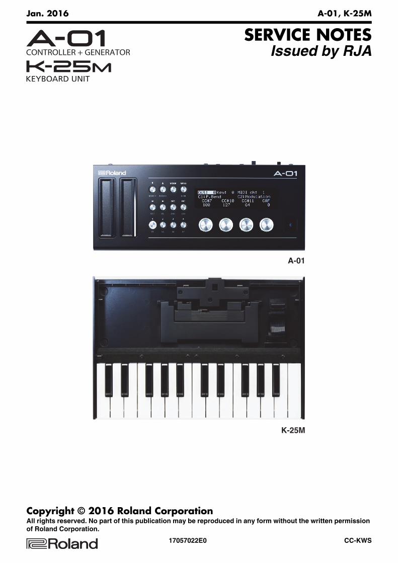
SERVICE NOTESIssued by RJA
Copyright © 2016 Roland CorporationAll rights reserved. No part of this publication may be reproduced in any form without the written permission of Roland Corporation.
CC-KWS17057022E0
Jan. 2016 A-01, K-25M
A-01
K-25M
Jan. 2016 A-01, K-25M
Table of ContentsCautionary Notes ..............................................................2Specifications .....................................................................3Location of Controls (A-01) .............................................4Exploded View (A-01) ......................................................6Exploded View (A-01) Parts List.....................................7Plain View (A-01) ..............................................................8Exploded View (K-25M).................................................10Exploded View (K-25M) Parts List ...............................11Plain View (K-25M).........................................................12Disassembly Procedure ..................................................13Block Diagram/Wiring Diagram..................................14Parts List (A-01) ...............................................................16Parts List (K-25M) ...........................................................18Verifying the Version .....................................................19Data Backup and Restore Operations ..........................19Performing a Factory Reset............................................19Updating the System ......................................................19Test Mode.........................................................................20Circuit Board (Main Board) ...........................................24Circuit Diagram (Main Board: 1/3)..............................26Circuit Diagram (Main Board: 2/3)..............................28Circuit Diagram (Main Board: 3/3)..............................30Circuit Board (Panel, Sensor Board).............................32Circuit Diagram (Panel Board)......................................34Circuit Diagram (Sensor Board)....................................36
Cautionary Notes
Before beginning the procedure, please read through this document. The matters described may differ according to the model.
Back Up User Data!User data may be lost during the course of the procedure. Refer to Data Backup and Restore Operations (p. 19) in the Service Notes and save the data. After completing the procedure, restore the backed-up data to the product.
Part ReplacementWhen replacing components near the power-supply circuit or a heat-generating circuit (such as a circuit provided with a heat sink or including a cement resistor), carry out the procedure according to the instructions with respect to the part number, direction, and attachment position (mounting so as to leave an air gap between the component and the circuit board, etc.).
Parts ListA component whose part code is ******** will not be supplied as a service part because one of the following reasons applies.
• Because it is supplied as an assembled part (under a different part code).
• Because a number of circuit boards are grouped together and supplied as a single circuit board (under a different part code).
• Because supply is prohibited due to copyright restrictions.
• Because reissuance is restricted.
• Because the part is made to order (at current market price).
• Because it is carried in electronic data on the Roland web site.
• Because it is a package or an accessory irrelevant to the function maintenance of the main body.
• Because it can be replaced with an article on the market. (battery or etc.)
Circuit DiagramIn the circuit diagram, “NIU” is an abbreviation for “Not in Use,” and “UnPop” is an abbreviation for “Unpopulated.” They both mean non-mounted components. The circuit board and circuit board diagram show silk-screened indications, but no components are mounted.
2
Jan. 2016 A-01, K-25M
Specifications
Roland A-01: Controller + Generator
Memory
Controller Mode: 16 settings (4 settings x 4 banks)
Synth Mode: 16 patches (8 patches x 2 banks)
Seq Mode: 16 patterns (8 patterns x 2banks)
Connectors
PHONES jack: Stereo miniature phone type
CV OUT jack: Stereo miniature phone type
GATE OUT jack: Stereo miniature phone type
MIDI (IN, OUT) connectors
USB port: MicroB type (MIDI)
Bluetooth
Bluetooth(R) Smart
Power Supply
Rechargeable Ni-MH battery (AA, HR6) x 4
Alkaline battery (AA, LR6) x 4
USB bus power
Current Draw
500 mA (USB bus power)
Expected battery life under continuous use:
Rechargeable Ni-MH battery: Approx. 12 hours
* This can vary depending on the specifications of the batteries, capacity of the batteries, and the conditions of use.
Dimensions
300 (W) x 128 (D) x 46 (H) mm
11-13/16 (W) x 5-1/16 (D) x 1-13/16 (H) inches
Weight (including batteries)
950g
2 lbs 2 oz
Accessories
Owner’s Manual (#5100047233)
Leaflet “USING THE UNIT SAFELY” (#********)
Alkaline battery (AA, LR6) (#********) x 4
Options (sold separately)
Keyboard unit: K-25m
* Printed matters will not be supplied after the end of the production. Then, download the electronic file from the Roland web site.
* In the interest of product improvement, the specifications and/or appearance of this unit are subject to change without prior notice.
Roland K-25m: Keyboard Unit
Connector
16 pin flat cable
Dimensions
308 (W) x 209 (D) x 44 (H) mm
12-1/8 (W) x 8-1/4 (D) x 1-3/4 (H) inches
Weight
700g
1 lb 9 oz
Accessories
Owner’s Manual (#5100047884)
Applicable Models
JU-06, JP-08, JX-03, A-01
* Printed matters will not be supplied after the end of the production. Then, download the electronic file from the Roland web site.
* In the interest of product improvement, the specifications and/or appearance of this unit are subject to change without prior notice.
3
Jan. 2016 A-01, K-25M
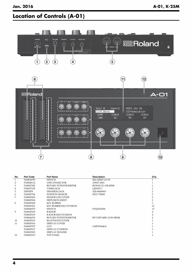
Location of Controls (A-01)fig.panel.eps
7 9
6 1211
5432
8 10
1
No. Part Code Part Name Description Q’ty1 5100036799 SWITCH SKI-22H07-G9-TS 12 5100048112 USB CONNECTOR 105017-0001 13 5100047382 ROTARY POTENTIOMETER RV09AF-21-15K-B50K 14 5100037105 3.5MM JACK LJE0393-7 35 02892878 DIN(MIDI) JACK 2DJ-00600003 26 5100047706 POSITION SENSOR FSLP 75MM 27 5100047003 SENSOR LED COVER 2
5100047004 DIFFUSION SHEET 28 5100047020 KEY RUBBER 3
5100047021 KEY RUBBER ESCUTCHEON 125100046575 SWITCH EVQP2202M 12
9 5100047018 R-KNOB 45100047019 R-KNOB ESCUTCHEON 45100046518 ROTARY POTENTIOMETER RV112FF-40B1-10.5F-0B20K 4
10 5100047015 BLUETOOTH COVER 111 5100047016 DISPLAY COVER 1
5100047707 LCD CMF2P2648-E 15100047017 DISPLAY CUSHION 15100047022 DISPLAY HOLDER 1
12 5100047013 TOP PANEL 1
4

Jan. 2016 A-01, K-25M
5
Jan. 2016 A-01, K-25M
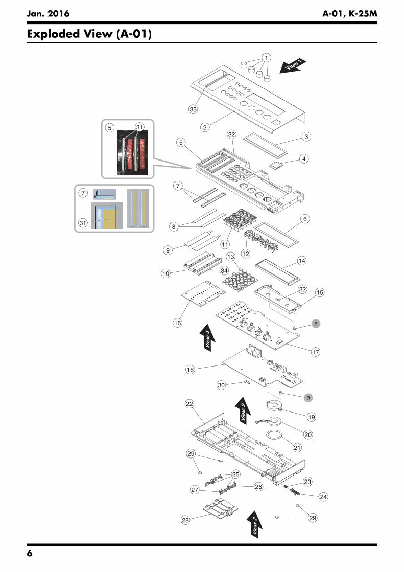
Exploded View (A-01)fig.bunkaizu.eps
7
9
8
10
2
5
4
3
1314
15
17
19
21
24
23
29
29
20
6
16
27
25
26
18
28
30
22a
315
7
31
11
12
1
a
Vie
w 3
Vie
w 2
Vie
w 4
View 1
32
32
33
34
6
Jan. 2016 A-01, K-25M
Exploded View (A-01) Parts List
No. Part Code Part Name Description Q’ty1 5100047018 R-KNOB 42 5100047013 TOP PANEL 13 5100047016 DISPLAY COVER 14 5100047015 BLUETOOTH COVER 15 5100047014 PANEL ESCUTCHEON 16 5100047017 DISPLAY CUSHION 17 5100047003 SENSOR LED COVER 28 5100047004 DIFFUSION SHEET 29 5100047706 POSITION SENSOR FSLP 75MM 210 5100047002 LED ESCUTCHEON 111 5100047021 KEY RUBBER ESCUTCHEON 1212 5100047019 R-KNOB ESCUTCHEON 413 5100047020 KEY RUBBER 314 5100047707 LCD CMF2P2648-E 115 5100047022 DISPLAY HOLDER 1
5100047033 PANEL SHEET ASSY 1* This unit includes the following parts.
16 ******** SENSOR BOARD 117 ******** PANEL BOARD 1
18 5100047034 MAIN BOARD ASSY 119 5100047007 SPEAKER HOLDER 120 5100047316 SPEAKER KDMG36008-10B 121 5100047006 SPEAKER CUSHION 122 5100047001 MODULE CASE 123 5100046998 COILED SPRING 124 5100047005 HINGE PIN R 125 5100047009 BATTERY TERMINAL +/- 326 5100047010 BATTERY TERMINAL + 127 5100047011 BATTERY TERMINAL - 128 5100047008 BATTERY COVER 129 5100047012 FOOT 430 5100048644 LEAF 131 40122490 DOUBLE-FACED TAPE #500 W5MM 20M 40P -32 40345056 DOUBLE-FACED TAPE #500 W10MM 20M 20P(CM) -33 40122534 DOUBLE-FACED TAPE #500 W3MM 20M 136P -34 40122612 ACETATE TAPE NITTO #5 BLACK W10MM 30M 20P -
a 40011312 SCREW 3X8 BINDING TAPTITE P FE BZC 4
7
Jan. 2016 A-01, K-25M
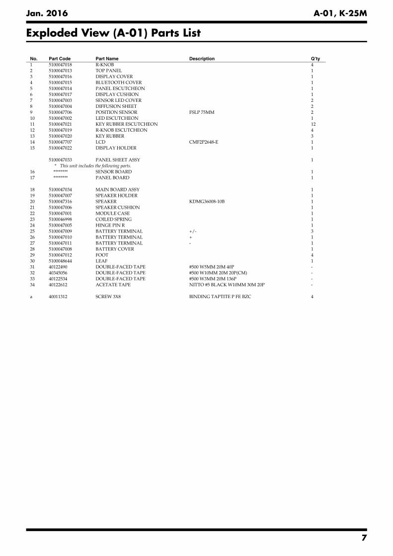
Plain View (A-01)fig.bunkaizu-H.eps
View 1
View 2
View 3
View 4
a
a
b
c
aaa
View 1 View 2
View 3 View 4
No. Part Code Part Name Description Q’tya 40011312 SCREW 3X8 BINDING TAPTITE P FE BZC 3
No. Part Code Part Name Description Q’tya 40011312 SCREW 3X8 BINDING TAPTITE P FE BZC 6c 40012956 SCREW M3X8 PAN MACHINE W/SW+PW FE BZC 2
No. Part Code Part Name Description Q’tya 40011312 SCREW 3X8 BINDING TAPTITE P FE BZC 4
No. Part Code Part Name Description Q’tya 40011312 SCREW 3X8 BINDING TAPTITE P FE BZC 11b 40011267 SCREW 3X6 BINDING TAPTITE P FE ZC 1
8

Jan. 2016 A-01, K-25M
9
Jan. 2016 A-01, K-25M
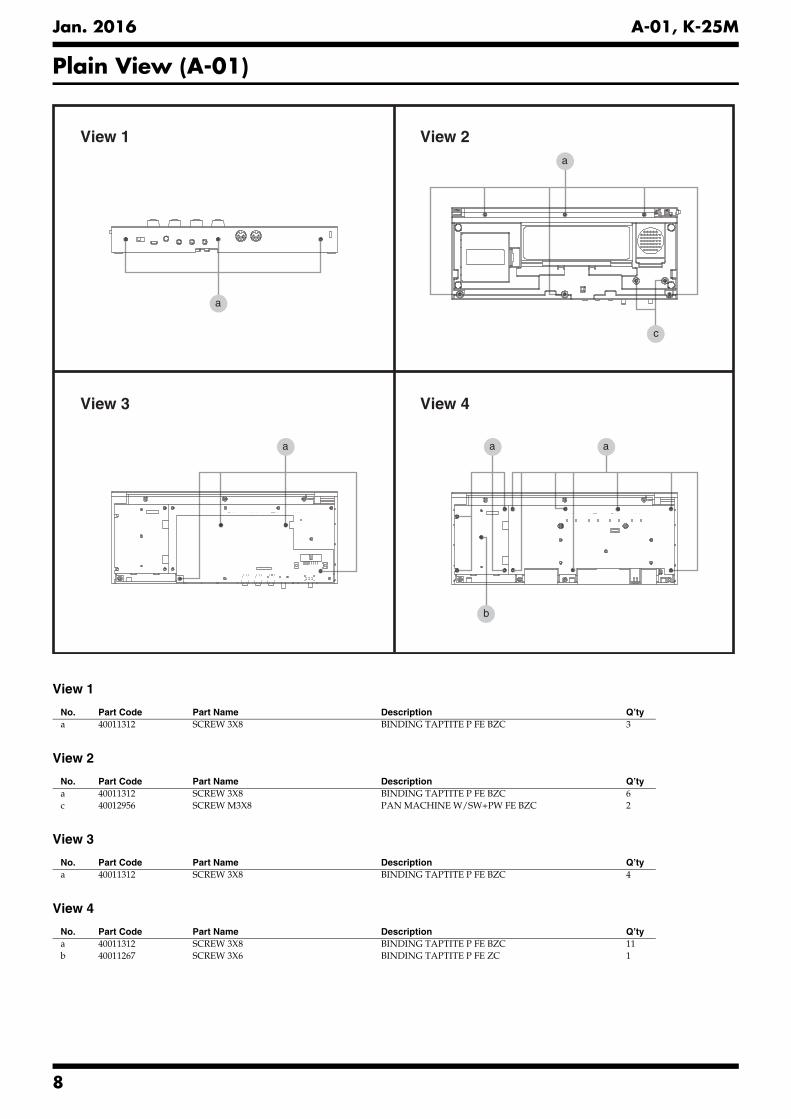
Exploded View (K-25M)fig.bunkaizu-K25M.eps
b
a
a
1
1523
21
22
9
6
16
7
10
11
1312
17
5
20
8
18
4
19
14
2
3
Vie
w 2
Vie
w 4
Vie
w 1
Vie
w 3
10
Jan. 2016 A-01, K-25M
Exploded View (K-25M) Parts List
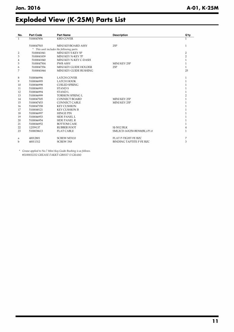
* Grease applied to No.7 Mini Key Guide Bushing is as follows.#5100032252 GREASE FAKKT-GB0557 (3 GRAM)
No. Part Code Part Name Description Q’ty1 5100047856 KBD COVER 1
5100047503 MINI KEYBOARD ASSY 25P 1* This unit includes the following parts.
2 5100041841 MINI KEY S-KEY 5P 23 5100041839 MINI KEY N-KEY 7P 24 5100041840 MINI KEY N-KEY C-DASH 15 5100047504 PWB ASSY MINI KEY 25P 16 5100047356 MINI KEY GUIDE HOLDER 25P 17 5100041844 MINI KEY GUIDE BUSHING 25
8 5100046996 LATCH COVER 19 5100046995 LATCH HOOK 110 5100046998 COILED SPRING 111 5100046993 STAND S 112 5100046994 STAND L 113 5100046999 TORSION SPRING L 214 5100047505 CONNECT BOARD MINI KEY 25P 115 5100047453 CONNECT CABLE MINI KEY 25P 116 5100047358 KEY CUSHION 117 5100048121 KEY CUSHION B 118 5100046997 HINGE PIN 119 5100046953 SIDE PANEL L 120 5100046954 SIDE PANEL R 121 5100046952 BOTTOM CASE 122 12359137 RUBBER FOOT SJ-5012 BLK 423 5100038613 FLAT CABLE SML2CD-16X250-BDX8(BL)-P1.0 1
a 40012801 SCREW M3X10 FLAT P-TIGHT FE BZC 7b 40011312 SCREW 3X8 BINDING TAPTITE P FE BZC 3
11
Jan. 2016 A-01, K-25M
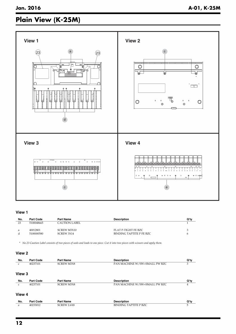
Plain View (K-25M)fig.bunkaizu-K25MH.eps
View 1
* No.23 Caution Label consists of two pieces of seals and leads to one piece. Cut it into two pieces with scissors and apply them.
View 2
View 3
View 4
a c
d
c e
2323
View 1 View 2
View 3 View 4
No. Part Code Part Name Description Q’ty23 5100048665 CAUTION LABEL 1
a 40012801 SCREW M3X10 FLAT P-TIGHT FE BZC 3d 5100000580 SCREW 3X14 BINDING TAPTITE P FE BZC 6
No. Part Code Part Name Description Q’tyc 40237101 SCREW M3X8 PAN MACHINE W/SW+SMALL PW BZC 3
No. Part Code Part Name Description Q’tyc 40237101 SCREW M3X8 PAN MACHINE W/SW+SMALL PW BZC 4
No. Part Code Part Name Description Q’tye 40233012 SCREW 2.6X8 BINDING TAPTITE P BZC 5
12
Jan. 2016 A-01, K-25M
Disassembly Procedure
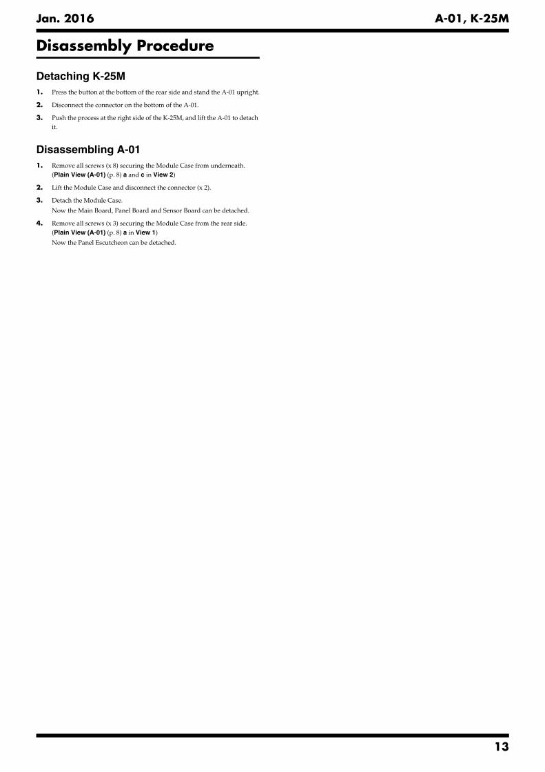
Detaching K-25M1. Press the button at the bottom of the rear side and stand the A-01 upright.
2. Disconnect the connector on the bottom of the A-01.
3. Push the process at the right side of the K-25M, and lift the A-01 to detach it.
Disassembling A-011. Remove all screws (x 8) securing the Module Case from underneath.
(Plain View (A-01) (p. 8) a and c in View 2)
2. Lift the Module Case and disconnect the connector (x 2).
3. Detach the Module Case.
Now the Main Board, Panel Board and Sensor Board can be detached.
4. Remove all screws (x 3) securing the Module Case from the rear side. (Plain View (A-01) (p. 8) a in View 1)
Now the Panel Escutcheon can be detached.
13
Jan. 2016 A-01, K-25M
M
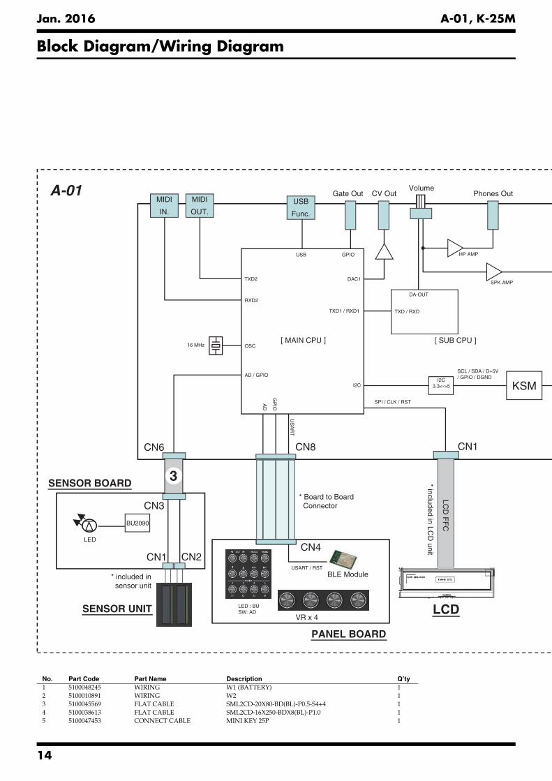
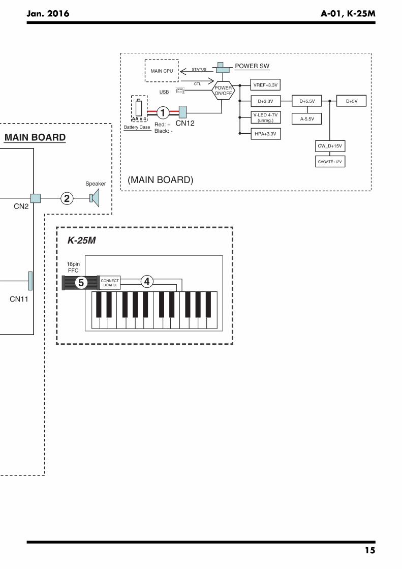
Block Diagram/Wiring Diagramfig.wiring-block.eps@L
USB
Func.
LED : BUSW: AD
VR x 4
US
AR
T
MIDI
IN.
MIDI
OUT.
KSI2C
SCL / SDA / D+5V/ GPIO / DGND
TXD / RXD
SPK AMP
VolumePhones Out
HP AMP
CV OutGate Out
BLE Module
LCD
FF
C
[ SUB CPU ]
CN8
CN4
CN6
CN3
CN1
SPI / CLK / RST
CN1 CN2USART / RST
LED
* included in sensor unit
USB
TXD2
RXD2
I2C
TXD1 / RXD1
DAC1
GPIO
OSC
AD / GPIO
[ MAIN CPU ]
GP
IO
AD
16 MHz
DA-OUT
3.3<->5
3SENSOR BOARD
SENSOR UNIT
PANEL BOARD
LCD
BU2090
* Board to Board Connector
* included in LCD
unit
A-01
No. Part Code Part Name Description Q’ty1 5100048245 WIRING W1 (BATTERY) 12 5100010891 WIRING W2 13 5100045569 FLAT CABLE SML2CD-20X80-BD(BL)-P0.5-S4+4 14 5100038613 FLAT CABLE SML2CD-16X250-BDX8(BL)-P1.0 15 5100047453 CONNECT CABLE MINI KEY 25P 1
14
Jan. 2016 A-01, K-25M
CN
CN1
MAI
fig.wiring-block.eps@R
POWER SW
USB
AA x 4
Speaker
POWERON/OFF
2
1
CN12
MAIN CPU
CTL
STATUS
2
1Battery Case
(MAIN BOARD)
CVGATE+12V
D+5.5V
A-5.5V
CW_D+15V
VREF+3.3V
V-LED 4-7V
D+3.3V
HPA+3.3V
D+5V
(unreg.)
45 CONNECTBOARD
K-25M
N BOARD
Red: +Black: -
16pinFFC
15

Jan. 2016 A-01, K-25M
Parts List (A-01)fig.-part1-e.eps
Note: The parts marked # are new. (initial parts) The description “Q’ty” means a necessary number of the parts per one product.
Due to one or more of the following reasons, parts with parts code ******** cannot be supplied as service parts.
• Supply is prohibited due to copyright restrictions. • It is carried in electronic data on the Roland web site. • The part is made to order (at current market price). • It can be replaced with an article on the market. (battery or etc.) • It is a package or an accessory irrelevant to the function maintenance of the main body. • A number of circuit boards are grouped together and supplied as a single circuit board (under a different part code).
• Reissuance is restricted. • It is supplied as an assembled part (under a different part code).
Safety Precautions:The parts marked have safety-related characteristics. Useonly listed parts for replacement.
CASING# 5100047013 TOP PANEL 1
5100047001 MODULE CASE 15100047008 BATTERY COVER 1
CHASSIS5100047002 LED ESCUTCHEON 1
# 5100047014 PANEL ESCUTCHEON 15100047007 SPEAKER HOLDER 1
KNOB, BUTTON# 5100047018 R-KNOB 4# 5100047020 KEY RUBBER 3
SWITCH5100036799 SWITCH SKI-22H07-G9-TS 1
# 5100046575 SWITCH EVQP2202M 12
JACK, EXT TERMINAL5100037105 3.5MM JACK LJE0393-7 302892878 DIN(MIDI) JACK 2DJ-00600003 25100048112 USB CONNECTOR 105017-0001 1
DISPLAY UNIT# 5100047707 LCD CMF2P2648-E 1
SPEAKER, BUZZER5100047316 SPEAKER KDMG36008-10B 1
PWB ASSY# 5100047034 MAIN BOARD ASSY 1
# 5100047033 PANEL SHEET ASSY 1* This unit includes the following parts.
******** PANEL BOARD 1 ******** SENSOR BOARD 1
POTENTIOMETER5100047382 ROTARY POTENTIOMETER RV09AF-21-15K-B50K 1
# 5100046518 ROTARY POTENTIOMETER RV112FF-40B1-10.5F-0B20K 4
WIRING, CABLE5100048245 WIRING W1 (BATTERY) 15100010891 WIRING W2 15100045569 FLAT CABLE SML2CD-20X80-BD(BL)-P0.5-S4+4 1
PICK UP, SENSOR5100047706 POSITION SENSOR FSLP 75MM 2
SCREWS40012956 SCREW M3X8 PAN MACHINE W/SW+PW FE BZC 240011267 SCREW 3X6 BINDING TAPTITE P FE ZC 140011312 SCREW 3X8 BINDING TAPTITE P FE BZC 28
16
Jan. 2016 A-01, K-25M
MISCELLANEOUS5100047012 FOOT 4
# 5100047021 KEY RUBBER ESCUTCHEON 12# 5100047019 R-KNOB ESCUTCHEON 4
5100047003 SENSOR LED COVER 2# 5100047015 BLUETOOTH COVER 1# 5100047016 DISPLAY COVER 1# 5100047022 DISPLAY HOLDER 1
5100046998 COILED SPRING 15100047005 HINGE PIN R 15100048644 LEAF 112199599 GRAND TERMINAL M3 2
# 5100047017 DISPLAY CUSHION 15100047006 SPEAKER CUSHION 15100047004 DIFFUSION SHEET 25100047010 BATTERY TERMINAL + 15100047011 BATTERY TERMINAL - 15100047009 BATTERY TERMINAL +/- 340122612 ACETATE TAPE NITTO #5 BLACK W10MM 30M 20P -40122534 DOUBLE-FACED TAPE #500 W3MM 20M 136P -40122490 DOUBLE-FACED TAPE #500 W5MM 20M 40P -40345056 DOUBLE-FACED TAPE #500 W10MM 20M 20P(CM) -
ACCESSORIES (Standard)# 5100047233 OWNER'S MANUAL MULTILANGUAGE 1
17
Jan. 2016 A-01, K-25M
Parts List (K-25M)fig.-part1-e.eps
Note: The parts marked # are new. (initial parts) The description “Q’ty” means a necessary number of the parts per one product.
Due to one or more of the following reasons, parts with parts code ******** cannot be supplied as service parts.
• Supply is prohibited due to copyright restrictions. • It is carried in electronic data on the Roland web site. • The part is made to order (at current market price). • It can be replaced with an article on the market. (battery or etc.) • It is a package or an accessory irrelevant to the function maintenance of the main body. • A number of circuit boards are grouped together and supplied as a single circuit board (under a different part code).
• Reissuance is restricted. • It is supplied as an assembled part (under a different part code).
Safety Precautions:The parts marked have safety-related characteristics. Useonly listed parts for replacement.
CASING# 5100046953 SIDE PANEL L 1# 5100046954 SIDE PANEL R 1# 5100046952 BOTTOM CASE 1
KEYBOARD ASSY# 5100047503 MINI KEYBOARD ASSY 25P 1
* This unit includes the following parts. 5100041839 MINI KEY N-KEY 7P 2 5100041840 MINI KEY N-KEY C-DASH 1 5100041841 MINI KEY S-KEY 5P 2
# 5100047356 MINI KEY GUIDE HOLDER 25P 1 5100041844 MINI KEY GUIDE BUSHING 25
# 5100047504 PWB ASSY MINI KEY 25P 1 40237101 SCREW M3X8 PAN MACHINE W/SW+SMALL PW BZC 4 40233012 SCREW 2.6X8 BINDING TAPTITE P BZC 5
PWB ASSY# 5100047505 CONNECT BOARD MINI KEY 25P 1
WIRING, CABLE5100038613 FLAT CABLE SML2CD-16X250-BDX8(BL)-P1.0 1
# 5100047453 CONNECT CABLE MINI KEY 25P 1
SCREWS40237101 SCREW M3X8 PAN MACHINE W/SW+SMALL PW BZC 340012801 SCREW M3X10 FLAT P-TIGHT FE BZC 1040011312 SCREW 3X8 BINDING TAPTITE P FE BZC 35100000580 SCREW 3X14 BINDING TAPTITE P FE BZC 6
MISCELLANEOUS# 5100046994 STAND L 1# 5100046993 STAND S 1# 5100046996 LATCH COVER 1# 5100046995 LATCH HOOK 1
12359137 RUBBER FOOT SJ-5012 BLK 4# 5100046999 TORSION SPRING L 2
5100046998 COILED SPRING 1# 5100046997 HINGE PIN 1# 5100047856 KBD COVER 1# 5100047358 KEY CUSHION 1# 5100048121 KEY CUSHION B 1# 5100048665 CAUTION LABEL 1
5100032252 GREASE FAKKT-GB0557 (3 GRAM) -
ACCESSORIES (Standard)# 5100047884 OWNER'S MANUAL MULTILANGUAGE 1
18
Jan. 2016 A-01, K-25M
Verifying the Version1. Hold down and turn on the power.
When Version is displayed on the screen, release .
The version of the main program is displayed.
2. Press 2.
The Boot version is displayed.
3. Press 3.
The Synth version is displayed.
When 1 is pressed, the version display of the main program returns.
4. Press MENU.
The unit moves to the normal mode.
Data Backup and Restore Operations
Items Required• Computer
• USB cable (type-A <-> type-micro B)
• MIDI sequence program (Cakewalk Sonar LE or etc.)
* Install this on the computer above beforehand.
Backup Operation1. Connect the computer to the USB connector ( ).
2. Turn on the power to the computer and the A-01.
3. Press MENU on the A-01.
The Select Menu screen appears.
4. When System is selected (Press [INC] at the right side of System: is highlighted), press INC.
5. Press or to select Bulk Dump, then press INC.
* Bulk Dump is on the second line from the last on the menu.
The Bulk Dump screen appears.
6. Start the MIDI sequence program on the computer, and set the MIDI device (input) to A-01, and put the system in standby for receiving SysEx data.
7. Press 4 on the A-01.
Executing... on the screen of the A-01 is displayed and SysEx data transmission starts.
When transmission finishes, Completed. is displayed.
8. Press DEC.
9. Save the received SysEx data on the MIDI sequence program.
10. Quit the MIDI sequence program and detach the USB cable.
Restore Operation1. Connect the computer to the USB connector ( ).
2. Turn on the power to the computer and the A-01.
3. Start the MIDI sequence program on the computer, and set the MIDI device (output) to A-01, and send the SysEx data which have been backed up.
Receiving bulkdump... is displayed on the screen of the A-01 and data receiving starts.
When the message disappears, receiving and writing have finished.
4. Quit the MIDI sequence program and detach the USB cable.
Performing a Factory Reset
For ver. 1.01 or earlier
1. Hold down and turn on the power.
Continue to hold down until Factory Reset Executing... appears.
When Completed. appears, the factory reset has finished.
2. Reset the power.
For ver. 1.02 or later
1. Hold down and turn on the power.
2. To execute the factory reset, press 4. To cancel it, press DEC.
When Completed. appears, the factory reset has finished.
3. Reset the power.
Updating the System
Items Required• Computer (running Windows)
• USB cable (type-A <-> type-micro B)
• Update program (obtained via Service Net)
• UpdSMF.exe (obtained via Service Information No. 102333.)
Procedure1. Connect the computer to the USB connector ( ).
2. Hold down 1 and turn on the power.
A-01 Updater appears on the screen.
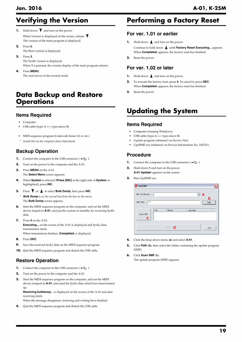
3. Run UpdSMF.exe.fig.update-1-e.eps
4. Click the drop-down menu (a) and select A-01.
5. Click Path (b), then select the folder containing the update program (SMF).
6. Click Scan SMF (c).
The update program (SMF) appears.
b
c
d
a
19
Jan. 2016 A-01, K-25M
7. Click Send (d).
Sending of the update program starts.fig.update-2.eps
While sending, 1 and LEDs of the ribbon controller at the leftmost of the panel flash.
When the update has finished, Complete is displayed on the screen of the A-01 and the following dialog box appears on the screen of the computer.
fig.update-3.eps
8. Click OK on the screen of the computer to quit UpdSMF.exe.
9. Turn off the power to the A-01.
Test Mode
Items Required• Computer (running Windows)
• USB cable (type-A <-> type-micro B)
• MIDI cable
• Dummy plug (monaural miniature)
• K-25M
• Noise meter
• Tester (measurable to 1 mV)
• Stabilized power supply unit
• Mobile device capable of Bluetooth LE (iPhone, iPad or etc.: iOS 9 or later)
• Software program capable of Bluetooth MIDI (GarageBand or etc.: the latest version)
* Install it to the mobile device capable of Bluetooth LE just described.
Test Items1. Battery AD Check (Battery AD) (p. 21)
2. Version Check (Version) (p. 21)
3. Device Check (Device) (p. 21)
4. LED Check (LEDs) (p. 21)
5. LCD Check (p. 21)
6. Switch Check (Buttons) (p. 21)
7. Encoder Check (Knobs) (p. 21)
8. Ribbon Controller Calibration (Calibration Ribbons) (p. 21)
9. Ribbon Controller Check (Ribbons) (p. 21)
10. Keyboard Check (Keyboard) (p. 22)
11. Jack Sense Check (Jacks) (p. 22)
12. Audio Check (Synth) (p. 22)
13. Bluetooth Check (Bluetooth) (p. 22)
14. GATE Check (Gate Voltage) (p. 22)
15. CV Calibration (CV Calibration) (p. 22)
16. Factory Reset (Factory Reset) (p. 23)
Entering the Test Mode
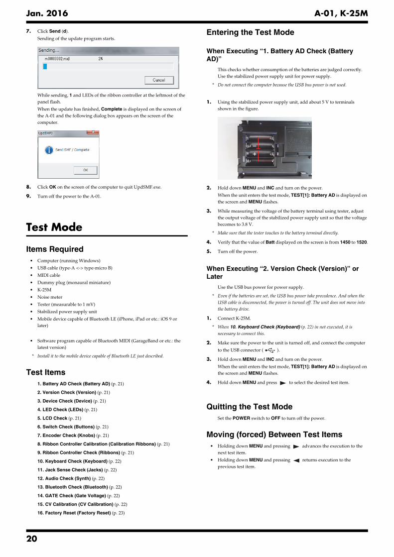
When Executing “1. Battery AD Check (Battery AD)”
This checks whether consumption of the batteries are judged correctly. Use the stabilized power supply unit for power supply.
* Do not connect the computer because the USB bus power is not used.
1. Using the stabilized power supply unit, add about 5 V to terminals shown in the figure.
fig.battery-case.eps
2. Hold down MENU and INC and turn on the power.
When the unit enters the test mode, TEST[1]: Battery AD is displayed on the screen and MENU flashes.
3. While measuring the voltage of the battery terminal using tester, adjust the output voltage of the stabilized power supply unit so that the voltage becomes to 3.8 V.
* Make sure that the tester touches to the battery terminal directly.
4. Verify that the value of Batt displayed on the screen is from 1450 to 1520.
5. Turn off the power.
When Executing “2. Version Check (Version)” or Later
Use the USB bus power for power supply.
* Even if the batteries are set, the USB bus power take precedence. And when the USB cable is disconnected, the power is turned off. The unit does not move into the battery drive.
1. Connect K-25M.
* When 10. Keyboard Check (Keyboard) (p. 22) in not executed, it is necessary to connect this.
2. Make sure the power to the unit is turned off, and connect the computer
to the USB connector ( ).
3. Hold down MENU and INC and turn on the power.
When the unit enters the test mode, TEST[1]: Battery AD is displayed on the screen and MENU flashes.
4. Hold down MENU and press to select the desired test item.
Quitting the Test ModeSet the POWER switch to OFF to turn off the power.
Moving (forced) Between Test Items• Holding down MENU and pressing advances the execution to the
next test item.
• Holding down MENU and pressing returns execution to the previous test item.
20

Jan. 2016 A-01, K-25M
1. Battery AD Check (Battery AD)This checks whether consumption of the batteries are judged correctly.
Follow When Executing “1. Battery AD Check (Battery AD)” (p. 20) and execute this.
* When executing 2. Version Check (Version) or later, follow When Executing “2. Version Check (Version)” or Later (p. 20) and change the connection of the power supply.
2. Version Check (Version)Verify each version.
The APP version and BOOT version are displayed.
1. Press 2.
The Synth version is displayed.
When 1 is pressed, the display of APP version and BOOT version returns.
2. Before advancing to the next test item, use the MIDI cable to connect the MIDI IN and MIDI OUT connectors.
3. Press MENU to advance to the next test item.
3. Device Check (Device)The operation of each device is checked automatically.
The operations of USB, MIDI and EEPROM are checked and the result is displayed on the screen.
1. Detach the MIDI cable.
2. Press MENU to advance to the next test item.
* Even if NG (not OK) is appears, you can advance to the next test item by MENU + .
4. LED Check (LEDs)This checks whether each LED lights up correctly.
All buttons light up.
1. Press MENU.
All buttons go dark.
2. Press MENU to advance to the next test item.
5. LCD CheckThis checks whether LCD operates correctly.
All dots of the LCD light up.
1. Press MENU.
All dots go dark.
2. Press MENU.
Dots light up in grid form.
3. Press MENU.
Dots light up in reverse---the grid form is highlighted.
4. Press MENU to advance to the next test item.
6. Switch Check (Buttons)This checks whether switches operate correctly.
1. Press the flashing buttons in sequence.
* When the wrong button is pressed, the error message appears on the screen. In this case, follow Moving (forced) Between Test Items (p. 20) and enter this test item again.
All buttons have been pressed, All buttons are OK. appears on the screen.
2. Press MENU to advance to the next test item.
7. Encoder Check (Knobs)This checks whether encoder operates correctly.
Check Enc1 is displayed.
1. Turn the leftmost knob clockwise.
turn right Enc1 is displayed.
2. Turn the knob until the value becomes 300.
turn left Enc1 is displayed.
3. Turn the knob counterclockwise until the value becomes 0.
Enc1 is OK. is displayed.
4. In the same way, check the operation of each knob in the sequence of the second knob from the left (Enc2), the third knob from the left (Enc3) and the rightmost knob (Enc4).
All Encoders are OK. is displayed.
5. Press MENU to advance to the next test item.
8. Ribbon Controller Calibration (Calibration Ribbons)This makes calibration of the ribbon controllers.
1. While pressing the upper end of the left ribbon controller, press 1.
2. While pressing the lower end of the left ribbon controller, press 1.
3. While pressing the upper end of the right ribbon controller, press 1.
4. While pressing the lower end of the right ribbon controller, press 1.
* When Touch. is displayed, calibration is not carried out correctly. In this case, follow Moving (forced) Between Test Items (p. 20) and enter this test item again.
5. Press MENU to advance to the next test item.
9. Ribbon Controller Check (Ribbons)This verifies whether the ribbon controllers detect the finger position correctly.
* When sliding on the ribbon controller, slide slowly without releasing your finger. Put a nail on the ribbon controller and rub it lightly, then inspection may succeed.
* When Error is displayed, follow Moving (forced) Between Test Items (p. 20) and enter this test item again.
The LED next to the left ribbon controller flashes and Check Ribbon1 is displayed on the screen.
1. Press the center of the left ribbon controller with a finger.
Flashing of the LED bar changes to lighting of the lower half and Ribbon1: Slide to bottom. is displayed on the screen.
2. Without releasing your finger as it is, slide slowly to the lowermost position.
The lighting of the LED bar follows the movement of finger and Ribbon1: Slide to top. is displayed on the screen.
21
Jan. 2016 A-01, K-25M
3. Without releasing your finger as it is, slide slowly to the uppermost position.
The lighting of the LED bar follows the movement of finger and Ribbon1: Slide to bottom again. is displayed on the screen.
4. Without releasing your finger as it is, slide slowly to the lowermost position.
The lighting of the LED bar follows the movement of finger and Release Ribbon1. is displayed on the screen.
5. Release your finger.
6. Check the right ribbon controller in the same way.
All Ribbons are OK. is displayed.
7. Press MENU to advance to the next test item.
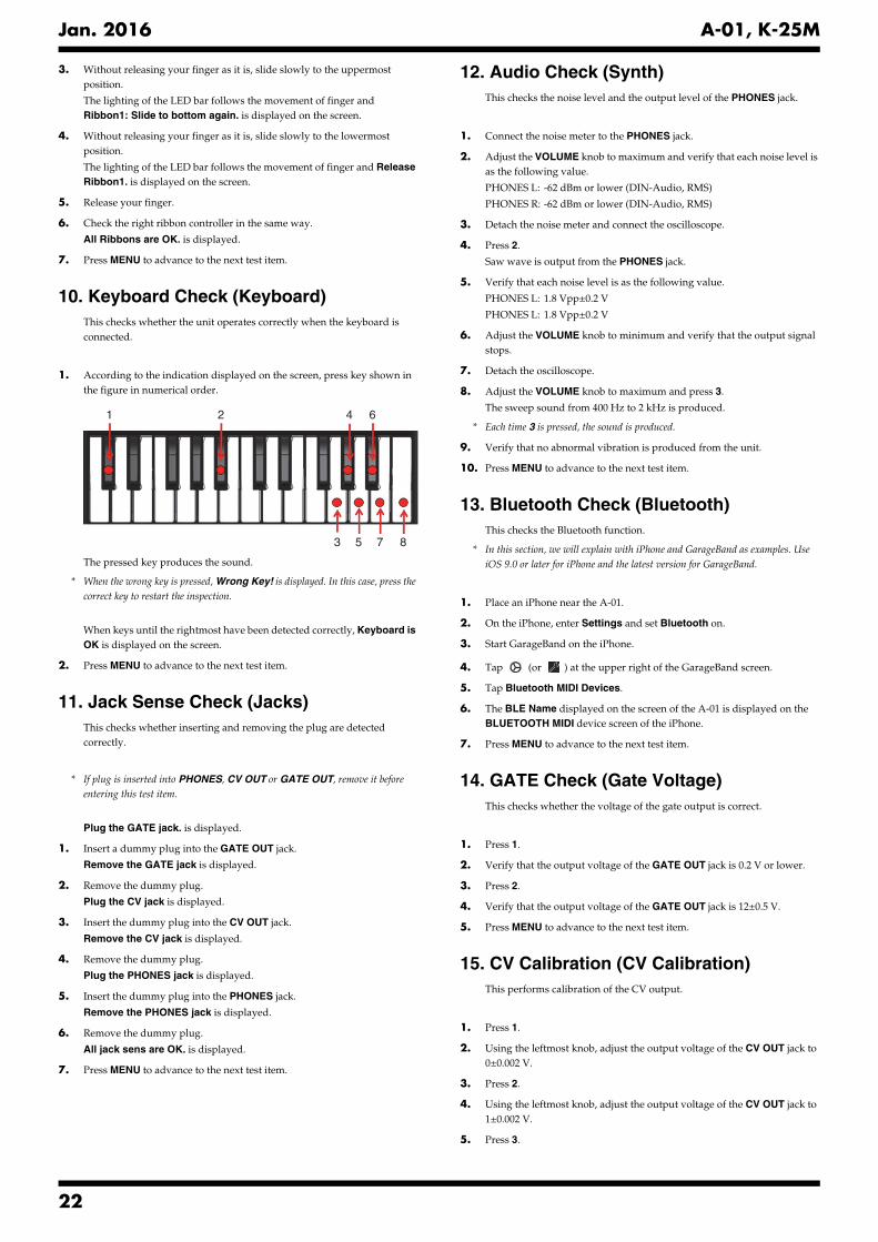
10. Keyboard Check (Keyboard)This checks whether the unit operates correctly when the keyboard is connected.
1. According to the indication displayed on the screen, press key shown in the figure in numerical order.
fig.test-key.eps
The pressed key produces the sound.
* When the wrong key is pressed, Wrong Key! is displayed. In this case, press the correct key to restart the inspection.
When keys until the rightmost have been detected correctly, Keyboard is OK is displayed on the screen.
2. Press MENU to advance to the next test item.
11. Jack Sense Check (Jacks)This checks whether inserting and removing the plug are detected correctly.
* If plug is inserted into PHONES, CV OUT or GATE OUT, remove it before entering this test item.
Plug the GATE jack. is displayed.
1. Insert a dummy plug into the GATE OUT jack.
Remove the GATE jack is displayed.
2. Remove the dummy plug.
Plug the CV jack is displayed.
3. Insert the dummy plug into the CV OUT jack.
Remove the CV jack is displayed.
4. Remove the dummy plug.
Plug the PHONES jack is displayed.
5. Insert the dummy plug into the PHONES jack.
Remove the PHONES jack is displayed.
6. Remove the dummy plug.
All jack sens are OK. is displayed.
7. Press MENU to advance to the next test item.
12. Audio Check (Synth)This checks the noise level and the output level of the PHONES jack.
1. Connect the noise meter to the PHONES jack.
2. Adjust the VOLUME knob to maximum and verify that each noise level is as the following value.
PHONES L: -62 dBm or lower (DIN-Audio, RMS)
PHONES R: -62 dBm or lower (DIN-Audio, RMS)
3. Detach the noise meter and connect the oscilloscope.
4. Press 2.
Saw wave is output from the PHONES jack.
5. Verify that each noise level is as the following value.
PHONES L: 1.8 Vpp±0.2 V
PHONES L: 1.8 Vpp±0.2 V
6. Adjust the VOLUME knob to minimum and verify that the output signal stops.
7. Detach the oscilloscope.
8. Adjust the VOLUME knob to maximum and press 3.
The sweep sound from 400 Hz to 2 kHz is produced.
* Each time 3 is pressed, the sound is produced.
9. Verify that no abnormal vibration is produced from the unit.
10. Press MENU to advance to the next test item.
13. Bluetooth Check (Bluetooth)This checks the Bluetooth function.
* In this section, we will explain with iPhone and GarageBand as examples. Use iOS 9.0 or later for iPhone and the latest version for GarageBand.
1. Place an iPhone near the A-01.
2. On the iPhone, enter Settings and set Bluetooth on.
3. Start GarageBand on the iPhone.
4. Tap (or ) at the upper right of the GarageBand screen.
5. Tap Bluetooth MIDI Devices.
6. The BLE Name displayed on the screen of the A-01 is displayed on the BLUETOOTH MIDI device screen of the iPhone.
7. Press MENU to advance to the next test item.
14. GATE Check (Gate Voltage)This checks whether the voltage of the gate output is correct.
1. Press 1.
2. Verify that the output voltage of the GATE OUT jack is 0.2 V or lower.
3. Press 2.
4. Verify that the output voltage of the GATE OUT jack is 12±0.5 V.
5. Press MENU to advance to the next test item.
15. CV Calibration (CV Calibration)This performs calibration of the CV output.
1. Press 1.
2. Using the leftmost knob, adjust the output voltage of the CV OUT jack to 0±0.002 V.
3. Press 2.
4. Using the leftmost knob, adjust the output voltage of the CV OUT jack to 1±0.002 V.
5. Press 3.
1 2 4
3 5 7 8
6
22
Jan. 2016 A-01, K-25M
6. Using the leftmost knob, adjust the output voltage of the CV OUT jack to 3±0.005 V.
7. Press MENU to advance to the next test item.
16. Factory Reset (Factory Reset)This returns the settings to their factory defaults.
1. Press 1.
After several seconds, Complete. is displayed and the factory reset has finished.
This ends the test mode.
Turn off the power.
23
Jan. 2016 A-01, K-25M
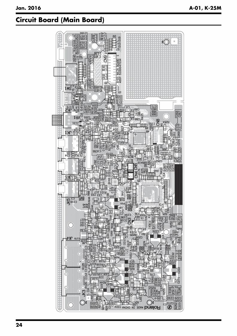
Circuit Board (Main Board)fig.b-main-1.eps
24
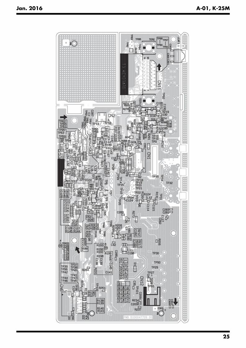
Jan. 2016 A-01, K-25M
fig.b-main-2.eps
25
Jan. 2016 A-01, K-25M
51-GPIO
-DET
P_VCC
ND
B-D-
B_PU
P_LOCXPRESS_GPIO
S-OFF
051-RST
CLK-CLK
CPU_TX-CLKCPU_RX-CLK
USB_PU
A-CLKL-CLK
SB-D+
D+3.3V
10kR78
1000
pFC8
9
106M010R
0.1uF87
TP10
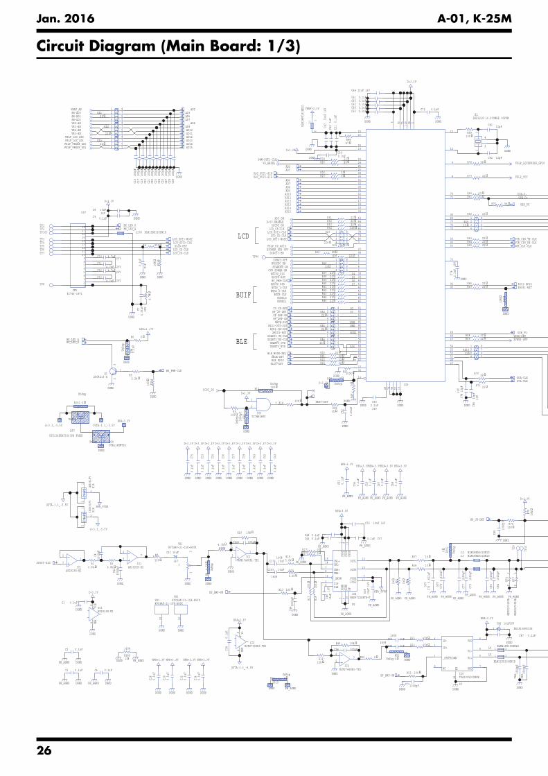
Circuit Diagram (Main Board: 1/3)fig.d-main-1.eps@L
FSLP_R0_GPIO
PH_AGND
DGND
80
PH_AGND
DGND
DCDC33-EN
VBUS
HPA+3.3V
DGND
AD6
D+3.3V
D+3.3V
PH_AGND
AD7
PH_AGND
D+3.3V
BK_LED_K
VREF+3.3V
DGND
DGND
D+3.3V
FSL
PH_AGND
DGND
XPOWER_KEY-OFF
DG
D+3.3V
AD6
DGND
AD7AD8AD9AD10AD11
SYOUT-SIG
US
AD12
US
AD13AD14
DGND
AD15
DGND
FSL
DGND
BUCK-CLK
HP_JK-DET
DGND
BUDO_1-CLK
DGND
BUDO_0-CLK
BUSEL1BUSEL0
BK_LED_A
VR_ABSEL
BK_LED_K
DGND
DGND
DGND
DGND
DGND
LCD_SPI3-MOSI
PH_AGND
BK_LED_A
DAC_OUT1-SIG
XLCD-RST
LED+4_+7V
PH_AGND
DAC_OUT2-SIG
DGND
LCD_CS-CLK
BLE_GPIO
HPA+3.3V
LCD_SPI3-CLK
DGND
XVBU
XRST-RST
BK_PWM-CLK
AD2
DGND
DGND
5DCDC_ON
N33_ON
PH_AGND
LCD_CS-CLK
X8
SUB_
D+5V-ENABLE
DGND
XMIDI-RST
VBAT_AD
PWM-OUT1-CLK
AD3
HPA+3.3V
SW-AD2
PH_AGND
SP_AMP-ON
SW-AD1
BK_PWM-CLK
HP_AMP-ON
SW-AD0
AD3
DGND
LCD_CD-CLK
AD2
DCDC_PG
DGND
SUB_
DGND
SUB_
D+3.3V
SD
MIDI-OUT-SIG
SC
MIDI-IN-SIG
U
GATE-SIG
DGND
HP_AMP-ON
DGND
PH_AGND
BLE_MODE-SEL
SP_AMP-ON
FSLP_LOC_AD1
OUTA-3.3_-5.5V
CV_JK-DET
FSLP_LOC_AD0
PH_AGND
HP_JK-DET
USART3_CTS
KSCPU_SIG
USART3_RTS
KSCPU-RST
PH_AGND
USART3_RX-CLKUSART3_TX-CLK
PH_AGND
AD12
DGND
XBLE-RST
AD13
DGND DGND
DGND DGND
PH_AGNDDGND
D+3.3V
DGND DGND
D+3.3V
DGND
D+3.3V
DGND
D+3.3V
DGND
D+3.3V
DGND
D+3.3V
DGND
D+3.3V
DGND
D+3.3V
DGND
D+3.3V
HPA+3.3V
PH_AGND PH_AGND
HPA+3.3V
PH_AGND
HPA+3.3V
PH_AGND
HPA+3.3V
PH_AGND
HPA+3.3V
HPA+3.3V
DGND
HPA+3.3V
DGND
HPA+3.3V
DGND
HPA+3.3V
DGND
DGNDPH_AGND
PH_AGND DGND PH_AGND DGND
PH_AGND
STANDBY-ONCVG_POWER-ON
XVBAT-OFFHVDCDC_EN
KSCPU_UPD
AD8VR0-AN
VR3-AN AD11
VR1-AN AD9VR2-AN AD10
FSLP_PRESS_AD0 AD14FSLP_PRESS_AD1 AD15
LCD_CD-CLKLCD_SPI3-MOSI
LCD_SPI3-CLK
XLCD-RST
DGND
DGND
DGND
DGND
DGND PH_AGND
HPA_PVSS
DGND
HPA+3.3VA-3.3_-5.5V OUTA-3.3_-5.5V
HPA_PVSS
A-3.3_-5.5V
OUTA-3.3_-5.5V
DGND
1k R54
1k R51
0R6
0R2720R271
L3 BLM18BD601SN1DL2 BLM18BD601SN1D
12R6112R60
1.5kR75
5.6kR15
5.6k
R16
10k
R17
10k
R18
6.8kR1
6.8kR3
TC7WH08FUIC3
1
27
4.7k
R8
UnPo
p
22RA10
1 8
654
32 7
22RA5
1 8
654
32 7
22RA9
1 8
654
32 7
22
RA21 8
654
32 7
220
RA7 1 8
654
32 7
22RA6
1 8
654
32 7
22RA1
1 8
654
32 7
22RA8
1 8
654
32 7
22RA4
1 8
654
32 7
22RA3
1 8
654
32 7
100
R7
L1
BLM1
8PG1
81SN
1D
21
10kR46
10kR19
22R6822R69
22R72
22R44
22R23
22R64
22R21
22R41
22R22
22R24
22R73
22R38
22R45
22R3922R40
22R71
22R63
22R37
22R67
22R36
22R65
22R43
22R66
22R30
22R70
22R31
22R25
22R32
22R62
22R33
22R35
22R20
22R42
0R4
9
0R29
UnPop
0R52
UnPop
0R270R26
0R50
100p
FC1
910
0pF
C20
100p
FC2
310
0pF
C24
100p
FC2
510
0pF
C27
100p
FC2
1
100pFC54
100p
FC2
8
100p
FC2
2
100p
FC2
9
100p
FC1
510
0pF
C17
1000pFC71
1000
pFC4
4
1000
pFC4
1000
pFC8
3
1000
pFC1
4
1000
pFC7
9
1000
pF
C85
1000
pFC8
8
1000
pFC8
4
1000
pFC7
7
1000
pFC4
0
UnPo
p
100R14
100R9
100R13
100R12
UnPop
100R53
100R74
100R59
47kR56
47kR55
EZJZ
1V33
0GA
R77
12
EZJZ
1V33
0GA
R76
12
10V10uF
NOJA
C86
12
IC1AK2923H-E2
57
6
IC1AK2923H-E2
31
2
AK2923H-E2IC1
4 VEE
8VD
D
25V4.7uFC11
25V4.7uFC10
25V4.7uFC12
25V4.7uFC13
C70 1uF1608
C69 1uF1608
5V
TPA2005D1DGNRIC6
4IN-
3IN+
1_SHUTDOWN
2NC
10PG
7GND
5VO+
8VO-
6VDD
2SC4213-AQ1
1
23
10R58
10R57
50V
52746-1871CN1
1817
23456789
10111213141516
1
16V
10uF
C5816V
10uF
C46
16V10uFC8
16V
10uF
C47
16V10uFC64
16V10uFC55
0.1uFC62
0.1uFC50
0.1uFC72
0.1uFC3 0.1uFC6
0.1uFC9
0.1u
FC5
1
0.1uF C57
0.1uFC1
0.1uFC48
C
0.1uFC63
0.1uFC65
0.1u
FC3
8
0.1uFC66
0.1u
FC3
9
0.1u
FC1
8UnPo
p
0.1uFC45
0.1u
FC7
5
0.1u
FC3
3
0.1u
FC3
5
0.1u
FC3
6
0.1u
FC3
7
0.1u
FC4
2
0.1u
FC4
3
0.1u
FC5
3
0.1u
FC5
6
0.1u
FC5
9
0.1u
FC6
7
0.1u
FC6
8
0.1u
FC3
0
0.1u
FC3
2
0.1u
FC3
4
0.1u
FC2
6
0.1uFC2
0.1u
FC4
1
0.1uFC61
12pFC81
12pFC82
DSX321G 16.000MHZ 30PPMX1
1
2
4
3
50V
10pF
C78
50V
10pF
C80
50V0.
022u
FC7
450V 0.
022u
FC7
3
25V
2.2u
FC7
6
25V2.2uFC60
IC2NJM2746RB1-TE1
57
6
IC2NJM2746RB1-TE1
31
2
NJM2746RB1-TE1IC2
4 GND
8 V+
5V
MAX9722AETE+TIC4
15INL+14INL-
7INR+8INR-
16_SHDN
3PG
ND6
SGND
20EP
9SV
DD
1PV
DD
SVDD
13
SVSS11
10OUTR
PVSS5
12OUTL
C1P24
C1N
L4 BLM21PG300SN1D21
L5
BLM21PG300SN1D
21
TP4
TP1
TP5
TP2
TP3
TP7
TP9
TP8
TP6
TP86
25V
0.33
uFC7
47R48
2.2kR5
R11 02012
UnPop
10k
R265
10k
R266
10k
R269
100kR47
4.7MR2
C49
1uF
VR1RV09AF-21-15K-B50K
1
3
2
RV09AF-21-15K-B50KVR1
10
RV09AF-21-15K-B50KVR1
20
C31 10uF
16V
C52
0.01
uF
1kR28
100pFC241
10kR10
0R289
1608
4.7kR288
0 R291
UnPo
p
10uFC1761608
10uFC293
1608
DTA114EMT2LQ24UnPop 11
33 22DTC114EUAT106(PB FREE)
Q23
UnPop
1
2 3
0R292
UnPop
1SS3
61FV
D15
3
21
1SS3
61FV
D18
3
21
IC5
7170
8
9
59606162
10075506
74 99 27 10
474851525354
676869
9596
73
919293
7276778990
7879807
12
13
1128
345383940414243444546
818283848586878855565758
979812
3794
14
49
2221
2019
23242526293031323536151617183334
63646566
TP103 L100 BLM15BD102SN1D
0.1u
F
C16
220R4
220R34
BUIF
BLENCE2
A16
NWENOE
D0D1
D2D3
D4D5D6D7
LCD
26
Jan. 2016 A-01, K-25M
PH_AGND
S
XC
DGND
R7
R8
L
16531024
TP13
TP12
SCN
1
SCN
2
ACM2012-900-2P-T00L6UnPop
1
2
10k
R268
0R290
fig.d-main-1.eps@R
AGND
8051-GPIO
VREF+3.3V
AGND
AGND
A-3.3_-5.5V
CVGATE+12V
AGND
AGND
DGND
DGND
VBUS+5V
DGND
D+3.3V
DGND
D+3.3V
DGND
D+3.3V
C2DEBUG-CLK
AGND
SUB_CPU_RX-CLK
DGND
C2DATA-CLK
AGND
SUB_CPU_TX-CLK
DGND DGND
D+3.3V
A-3.3_-5.5V
AGND
D+3.3V
AGND
DGND
DGND
DGND
DGND
D+5V
D+3.3V
DGND
AGND
DGND
XJRST
DGND
AGND
CVGATE+12V
CVGATE+12V
VBUS+5V
SYOUT-SIG
CVGATE+12V
AGND
A-3.3_-5.5V
AGND
AGND
AGND AGND
PWM-OUT1-CLK
D+5V
MIDI-IN-SIG
D+5V
DGND
DGND
DGND
XMIDI-RST
MIDI-OUT-SIG
D+5V
GATE-SIG
DAC_OUT2-SIG
SUB_CLK-CLK
DGND
X8051-RST
CV_JK-DET
DGND
D+3.3VAGND
AGND
DAC_OUT1-SIG
AGND DGND
AGND DGND
AGND DGND
AGND DGND
AGND DGND
DGND
DGND
D+3.3V
DGND
D+3.3V
SPI2_CLKPI2_DOUT
SPI2_DIN
S_EEPROM
DGND
USB_JK-D+
USB_JK-D-DGND
DGND
JTCK
JTMSJTDIJTDO
XRST-RST
DTC114EUAT106(PB FREE)
Q4
1
23
DTC114EUAT106(PB FREE)
Q2
1
23
DTC114EUAT106(PB FREE)
Q3
1
23
100R104
100R122
220R118
220R119
0R126
0R125
0R95UnPop
0R94
D1 1SS3
55 T
E-17
(PB
FREE
)Un
Pop
A1K2
L9 BLM18BD601SN1D
L12BLM18BD601SN1D
L8 BLM18BD601SN1D
L10 BLM18BD601SN1D
L11BLM18BD601SN1D
10kR85
0.5%
10k
R107
0.5%
10k
R98
0.5%
UnPo
p
10k
R99 0.
5%UnPo
p
10kR88
0.5%
10kR86
0.5%
UnPop
10k
R91
0.5%
10kR870.5%
10kR96
0.5%
10kR1020.5%
10kR930.5%
10kR90
0.5%
UnPop
10kR920.5%
UnPop
10k
R97 0.
5%
10kR112 UnPop
10kR113
0.5%
10k
R84
0.5%
10kR1010.5% 10kR103
0.5%
10k
R89
0.5%
TC7WH08FU
IC3
5
63
5.5V
TC7WH08FUIC3
GND
4VC
C8
1kR111
2DJ-
0060
0003
JK43
5241910
2DJ-
0060
0003
JK33
5241910
10k
RA11
1865
4 3 27
100
R109
10k
R106
10k
R132
22
R117
22R13022R129
22R116
22R128
0R110UnPop
0R83UnPop
09
00
0R105UnPop
100pFC95
UnPop
100pFC97
100pFC98
100pFC104
1000
pFC1
08
1000
pFC9
9
1000
pFC1
11
1000
pFC1
20
1000
pFC1
1310
00pF
C119
1000
pFC1
1410
00pF
C115
1000
pFC1
16
1000
pFC1
12
1000
pFC1
21
100R127
EZJZ
1V33
0GA
R133
12
EZJZ
1V33
0GA
R131
12DTC144EMT2L
Q61
23
1701S-116-02G2CN411
1701S-116-02G2CN422
1701S-116-02G2CN522
1701S-116-02G2CN511
1SS3
61FV
D4
3
21
1SS362FV
D2
2
3
1
1SS362FVD3
2
3
1
C901uF
1608
DTA1
14EM
T2L
Q5
DTA114EMT2L
11B
33C
22E
16V10uF
C107
16V10uFC109
0.1uFC125
0.1u
FC9
3
0.1uFC102
0.1uFC910.
1uF
C105
0.1uFC110
0.1uFC124
0.1uFC122
0.1uFC123
0.1uFC117
0.1uFC118
0.1u
FC1
03
0.1u
FC9
6
50V5pFC100
UnPop
50V5pF
C101UnPop
IC9QCPL-M614-500E
1
3
GND
4
5
VCC 6
IC7NJM062V(TE1)
57
6
IC8 NJM062V(TE1)
57
6
IC8NJM062V(TE1)
31
2
IC7NJM062V(TE1)
31
2
NJM062V(TE1)IC8
4 VEE
8VD
D
NJM062V(TE1)IC7
4 VEE
8VD
D
CN314FLT-SM2-TB (LF)(SN)50V
UnPop
11
22
33
44
55
66
88
99
1010
1111
1212
1313
1414
77
DSX321G 24.576MHZ 30PPM
X2UnPop
1
24
3
50V 0.
022u
FC9
2 50V 0.
022u
FC9
4
UnPo
p
10M
R115
UnPo
p
JK6LJE0393-7
16531024
JK5LJE0393-7
16531024
JK1JE0393-7
L7BLM21PG300SN1D
21
IC10
201
18
19
1545
1617
21
14
2
910111213
3
678
TP35
TP32
TP17
TP34
TP31
TP24
TP30
TP25
TP26
TP28
TP18
TP27
TP33
TP16
TP19
TP21
TP23
TP20
TP22
TP14
TP15
TP29
TP90
TP92
M02B-SRSS-TB (LF)(SN)2
M02B-SRSS-TB (LF)(SN)2
R1EX25064ATA00I#S0IC24
2Q5D6C
4VS
S8
VCC
_W3
_S1
_HOLD7
0.1uFC170
50V
33pF
C173Un
Pop
50V
33pF
C175
UnPo
p
2
3
4
47R123
120R121
470R124
1608
100kR82
1k R108
4.7k R120
220R114
180k R81
10kR100 0.5%
10kR2760.5%
C106100uF 16V
JK2105017-0001
40
10 20
30
54321
5060
1000
pFC1
85 UnPo
p
TP87TP88TP89
TP97
TP98
TP99
TP102
TP11
JTAG
MIDI IN
MIDI OUT
PHONESCV
GATE
27

Jan. 2016 A-01, K-25M
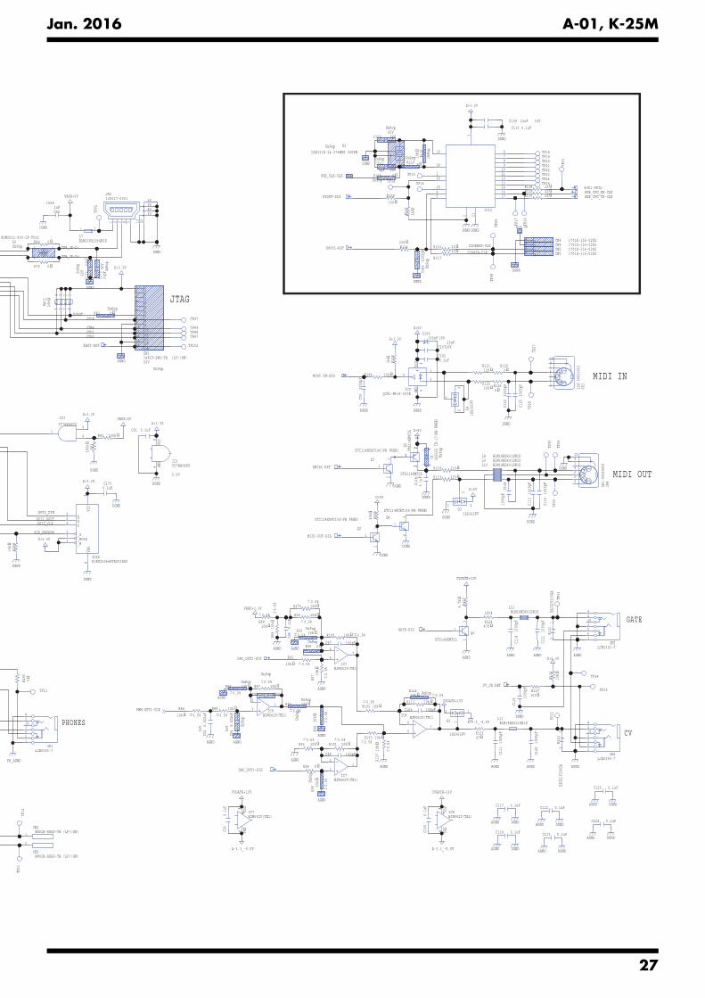
Circuit Diagram (Main Board: 2/3)fig.d-main-2.eps@L
KT6
D+5V
DGND
DGND
KPR5
DGND
D+5V
KSC4
KPR0
KT4
KPR6
DGND
DGND
KSC5
D+5V
KT5
KSC7
D+5V
DRIVE_2-2
SENSE-1
BUCK-CLK
KPR4
DRIVE_1-2
DGND
KSC3
KSC1KPR1
KT2
KSC0
DGND
KPR3
KT0
DGND
VREF+3.3V
DGND
DGND
D+5V
SENSE-2
DGND
DGND
DGND
DGND
D+5V
FSLP_VCC
DGND
SCL-CLK
D+5V
DRIVE_1-1
FSLP_R0_GPIO
FSLP_PRESS_AD0
5SDA-CLK
DGND
KSCPU-RST
DGND
VREF+3.3V
DGND
KPR7
FSLP_VCC
DRIVE_1-1
SDA-CLK
DRIVE_2-1
BUSEL0
5KSCPU_SIG_KB
SENSE-2
DGND
BUSEL1
FSLP_R0_GPIO
D+3.3V
FSLP_PRESS_AD1
5SCL-CLK
DGND
DGND
DGNDFSLP_LOC_AD1
D+5V
DGND
FSLP_LOCXPRESS_GPIO
DGND
DGND
FSLP_LOC_AD0
DRIVE_1-2
D+3.3V
DGND
SENSE-1
KSC6
FSLP_LOCXPRESS_GPIO
D+5V
BUDO_0-CLK
KT3
KSC2
DGND
DGND
5SCL-CLK
KSCPU_UPD
KT7
5SDA-CLK
DGND
KPR2
KSCPU_SIG
KT1
D+3.3V
VREF+3.3V
VREF+3.3V
DGND
LED_DGND DGND
LED_DGND DGND
LED+4_+7V
D+3.3V
D+3.3V LED_DGND
D+3.3V
DRIVE_2-1
DRIVE_2-2
DTC114EUAT106(PB FREE)
Q131
23
47k
R156
0.5%
UnPo
p47
kR1
530.
5%
UnPo
p
22RA15
1 8
654
32 7
22RA13
1 8
654
32 7
22RA12
1 8
654
32 7
22RA14
1 8
654
32 7
5.1k
R158
0.5%
UnPo
p5.
1kR1
570.
5%Un
Pop
10k
R180
10kR186
10kR204
10k
R18910k
R166
10k
R147
10k
R181
10k
R160
UnPo
p
22R198
22R203
22R200
22R197
22R199
22R196
22R20122R202
0R164UnPop
0R165
0R142
0R154UnPop
0R1720R173
0R191 UnPop
0R148
0R151UnPop
0R143
0R192 UnPop
0R162UnPop
0R169
0R171
0R161UnPop
0R139
0R1
78
0R138
0R159
0R152
0R137
0R1350R134
0R136
0 R177
0R1
76
0R168
0R193
0R140
0R155
0 R179
0R190
0R141
0R146
0R163UnPop
R150
100k
R149
100k
1000
pFC1
46
1000pFC147
100R195
100R194
UnPop
100R188
2.2k R144
2.2kR145
2.2k
R170
2.2k
R167
IC13AK2923H-E2
UnPop57
6
IC12AK2923H-E2
UnPop31
2
IC13AK2923H-E2
UnPop31
2
IC12AK2923H-E2
UnPop57
6
AK2923H-E2IC13UnPop
4 VEE
8VD
D
AK2923H-E2IC12UnPop
4 VEE
8VD
D
DTC114TUAT106Q7
12
3
RN1911FEQ11
UnPop 5
43
RN1911FEQ10
UnPop 2
16
RN1911FEQ10
UnPop 5
43
RN1911FEQ11
UnPop 2
16
DTA114EMT2LQ8
UnPop 1
32
DTA114EMT2LQ9
UnPop 1
32
0.1u
FC1
37
0.1u
FC1
31Un
Pop
0.1uFC140
0.1uFC145
0.1u
FC1
32Un
Pop
0.1u
FC1
36
0.1uFC143
0.1uFC126
0.1uFC129
25V
0.1uFC266
0.1uFC13025V
0.1uFC144
0.1u
FC1
3825
V
0.1uFC141
DSX321G 16.000MHZ 30PPMX3UnPo
p1
24
3
10pF
C128
UnPo
p
10pFC149
UnPop
10pFC133
10pF
C127UnPo
p
10pFC148
UnPop
10pFC134
PCA9306DCURIC11
4SDA13SCL1
8EN
1GN
D
2VR
EF1
VREF
27
5SDA2SCL2
6
MB9AF111LAPMC1-G-106JNE2
IC14
28PE0/MD1 29
MD031
PE3/X1
30PE2/X0
63P81 62P80
4P52/INT02_0/ZIN0_2/SCK3_1 3P51/INT01_0/BIN0_2/SOT3_1 2P50/INT00_0/AIN0_2/SIN3_1
27P4E/TIOB5_0/INT06_2/SIN7_1/ZIN1_2 26
P4D/TIOB4_0/SOT7_1/BIN1_2 25P4C/TIOB3_0/SCK7_1/AIN1_2 24
P4B/TIOB2_0/ZIN0_1 23P4A/TIOB1_0/BIN0_1 22P49/TIOB0_0/AIN0_1 20
P47/X1A 19P46/X0A
7P32/ZIN0_0/TIOB2_1/SOT6_1/INT05_2
43AV
SS
32VS
S
64VS
S17C
21INITX
P3F/RTO05_0/TIOA5_115
P3E/RTO04_0/TIOA4_114
P3D/RTO03_0/TIOA3_113
P3C/RTO02_0/TIOA2_112
P3B/RTO01_0/TIOA1_111
P3A/RTO00_0/TIOA0_110
P39/DTTI0X_0/ADTG_29
P33/INT04_0/TIOB3_1/SIN6_1/ADTG_68
P31/BIN0_0/TIOB1_1/SCK6_1/INT04_26
42AVRH
58P62/SCK5_0/ADTG_3
41AV
CC
50P01/TCK/SWCLK
52P03/TMS/SWDIO
60P60/SIN5_0/TIOA2_2/INT15_1
59P61/SOT5_0/TIOB2_2
VSS
161
VCC
18VC
C
33VC
C
5P30/AIN0_0/TIOB0_1/INT03_2
P23/SCK0_0/TIOA7_14647
P22/SOT0_0/TIOB7_1P21/SIN0_0/INT06_1
48
45P19/AN09/SCK2_2P18/AN08/SOT2_2
4440
P17/AN07/SIN2_2/INT04_1P15/AN05/IC03_2
3938
P14/AN04/INT03_1/IC02_2P13/AN03/SCK1_1/IC01_2
3736
P12/AN02/SOT1_1/IC00_2P11/AN01/SIN1_1/INT02_1/FRCK0_2
3534
P10/AN00
P0F/NMIX/CROUT_15756
P0C/SCK4_0/TIOA6_1P0B/SOT4_0/TIOB6_1
5554
P0A/SIN4_0/INT00_2P04/TDO/SWO
5351
P02/TDIP00/TRSTX
49
VCC
61
TP46
TP38TP39TP40
TP41
TP45
TP37
TP44TP43TP42
0.1uFC271
0.1uFC272
TP36
TP96
CN620FLZ-SM2-TB (LF)(SN)
50V
123456789
1011121314151617181920
50V
0.01
uF
C139
16V10uF
C14210uF16V
25V
4.7uFC135
DTC114TUAT106
Q121
23
10k
R278
0R1
87
1608
470R182
22R2
82
470R283UnPop
1MR1
74
100kR183
22R2
84
470R285 UnPop
1MR1
75
100kR185
470R184
From Bender Sensor
28
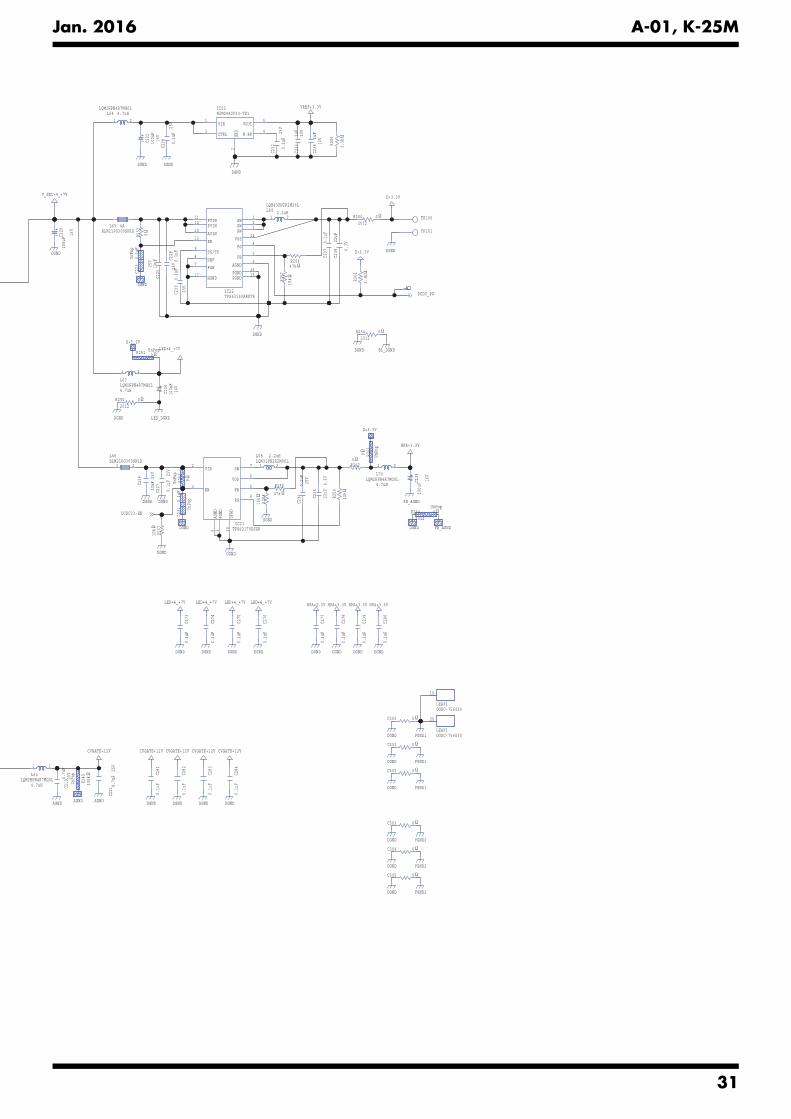
Jan. 2016 A-01, K-25M
BUCK-CLK
SW-AD2
SW-AD0SW-AD1
VR1-AN
VR3-AN
VR_ABSEL
VR2-AN
VR0-AN
BUSEL1BUSEL0
BUDO_1-CLK
fig.d-main-2.eps@R
LED+4_+7V D+3.3V
DGND
KPR7KSC6KPR6
KSC3KPR3KSC2KPR2
KSC0KPR0
KPR5
D+5V
KT4
DGND
KT3
KSC5
KSC7
DGND
KT7KT6KT5
KSC3KPR3KSC4KPR4KSC5KPR5KSC6KPR6
DGND
D+5V
DGND
D+5V
KT2KT1KT0
DGND
D+5V
KPR2KSC2KPR1KSC1
D+3.3V
DGND
LED_DGND
USART3_CTS
BLE_GPIO
XBLE-RST
USART3_RTSUSART3_TX-CLK
USART3_RX-CLK
BLE_MODE-SEL
DGND
VR1_B-ANVR2_B-ANVR3_B-AN
SW_B-AD0SW_B-AD1SW_B-AD2
VR0_B-ANVR_ABSEL_B
BUSEL1_BBUSEL0_B
BUDO_1_B-CLKBUCK_B-CLK
DGND
DGND
BLE_MODE_B-SELBLE_GPIO_B
USART3_TX_B-CLKUSART3_B_RTSUSART3_RX_B-CLKUSART3_CTS_B
XBLE_B-RST
DGND
DGNDBL_DGND
BL_DGND DGND
DGND
DGND
LED_DGND
LED_DGND
LED_DGND
LED+4_+7V
BL_DGND
LED_DGND
DGND
DGNDDGND
DGND
KPR4KSC4
KSC1KPR1
100p
FC1
69
100p
FC1
62Un
Pop
100p
FC1
60
100p
FC1
64Un
Pop
100p
FC1
54
100p
FC1
55
100p
FC1
52
100p
FC1
74
100p
FC1
57
100p
FC1
56
100p
FC1
63
100p
FC1
66Un
Pop
100p
FC1
65
100p
FC1
67
100p
FC1
68Un
Pop
100p
FC1
61
100p
FC1
71
100p
FC1
5810
0pF
C159
100p
FC1
53
1000
pFC2
47
1000
pFC2
5310
00pF
C252
1000
pFC2
50
1000
pFC2
5510
00pF
C254
1000
pFC2
62
1000
pFC2
65
1000
pFC2
58
1000
pFC2
5610
00pF
C257
1000
pFC2
60
1000
pFC2
49
1000
pFC2
5110
00pF
C248
1000
pFC2
6310
00pF
C264
1000
pFC2
59
1000
pFC2
61
47kRA19
1 8
654
32 7
47kRA16
1 8
654
32 7
47kRA17
1 8
654
32 7
47kRA18
1 8
654
32 7
1SS3
62FV
D20
2
3
1
1SS3
62FV
D22
2
3
1
1SS3
62FV
D8
2
3
1
1SS3
62FV
D11
2
3
1
1SS3
62FV
D5
2
3
1
1SS3
62FV
D24
2
3
1
1SS3
62FV
D7
2
3
1
1SS3
62FV
D10
2
3
1
1SS3
62FV
D13
2
3
1
1SS3
62FV
D62
3
1
1SS3
62FV
D92
3
1
1SS3
62FV
D12
2
3
1
1SS3
62FV
D16
2
3
1
1SS3
62FV
D19
2
3
1
1SS3
62FV
D14
2
3
1
1SS3
62FV
D17
2
3
1
L26
L32
L28
L25
L14
L29
L19
L45
L21
L42
L30
L20
L43
L38 UnPop
L18
L16
L17
L22
L40 UnPop
L15
L49
L31
L55
L54
L47L46
L39 UnPop
L51
L37 UnPop
L52
L50
L53L24
BLM15BD102SN1D
L23
L44
L27
L41
L48
BLM15BD102SN1D
0.1uFC172
0.1uFC151
0.1uF
C150
CN11HIF3FC-16PA-2.54DS
200V
11
22
33
44
55
66
77
88
99
1010
1111
1212
1313
1414
1515
1616
TP62
TP64
TP60
TP47
TP49
TP51
TP53
TP55
TP57
TP56
TP48
TP50
TP52
TP58
TP54
TP59
TP61
TP63
TP65
0.1uFC267
0.1uFC268
0.1uFC269
0.1uFC270
TP66TP67TP68TP69TP70TP71TP72TP73TP74TP75TP76TP77TP78TP79TP80TP81
TP82TP83TP84TP85
TP93
TP94
TP95
M1699TER1
12 3
4
M1699TER2
12 3
4
WR-40SB-VFH30-N1CN8
3636
3535
3434
3333
3232
3131
3030
2929
2828
2727
2626
2525
2424
2323
2222
2121
11223344556677889910101111121213131414151516161717181819192020
4040
3939
3838
3737
CN9
20FMN-BMTTN-A-TF (LF)(SN)
50V
UnPop
1 12 23 34 45 56 67 78 89 910 1011 1112 1213 1314 1415 1516 1617 1718 1819 1920 20
16V10uFC177
22R287
to PANEL
29
Jan. 2016 A-01, K-25M
.3V
VBAT_AD
GND
GND
A-3.3_-5.5V
0.1u
FC2
92
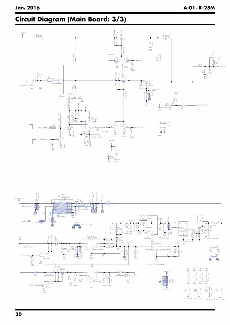
Circuit Diagram (Main Board: 3/3)fig.d-main-3.eps@L
DGND
XVBAT-OFF
DGNDDGND
P-ON
DGND
DGND
DGND
DGND DGND
DGND
DCDC_PG
DGND
HVDCDC_EN
DGND
DGND
D+3
STANDBY-ON
DGND
D+5.5V
XPOWER_KEY-OFFDGND
D+5V-ENABLE
DGND
VBAT+7V
DGND
DGND
N33_ON
D+3.3V
DGND
DGND
DGND
D+5V
D+3.3V
AGND
DGNDDGND
A-3.3_-5.5V
DGND
VSW+4V
DGNDDGND
DGND
DGNDDGND
DGNDDGND
VSW+4V
DGND
DGND
DGND
DGND
DGND
AGNDDGND
V_SRC+4_+7V
VBUS+5V
5DCDC_ON
DGND
HVDCDC_EN
DGND
AGND
CVGATE+12V
A-3.3_-5.5V
DGND
CVG_POWER-ON
ADGND
DGND A
DGND
D+5V
DGND
D+5V
DGND
D+5V
DGND
D+5V
A-3.3_-5.5V
DGND
A-3.3_-5.5V
DGND DGND DGND
DGND
DGND
AGND
CW_D+15V
D+3.3V
XVBUS-OFF
DGND
DGND
DGND
OUTA-3.3_-5.5V OUT
0R248
0R227
UnPop
IC16TC7WH74FU
5.5V
D2
CK1
_CR
6
_Q3
Q5
_PR
7
5.5VTC7WH74FU
IC164GN
D8
VCC
5.6kR223
UnPop
10k
R220
UnPo
p
100kR243
47k
R244
47kR2190.5%
C205
100u
F
16V
82kR221
UnPop
NJM2882F05-TE1IC19
1VIN
3CTRL
2GN
D 4N-BP
5VOUT
10k
R240
10k
R234
10k
R211
UnPo
p
10k
R213
0R239
0
R205UnPop
0
R224
0R2
38Un
Pop
1.5k
R215
1.5kR216
100k
R228
100k
R212
100k
R233
100k
R226
UnPo
p
100k
R222
UnPo
p
100k
R210
100k
R229
100kR235
100kR236
D37
RB160M-40TR
A1
K2
D33
RB160M-40TR
1 2
D31
RB160M-40TRUnPop
A1
K2
D36
RB16
0M-4
0TRA 1
K 2
100R225
100R209UnPop
100R241
1kR214 22k
R231
1kR237
22k
R230
1k R208
1kR206UnPop
1k R207
1SS4
22D34
2
3
11S
S422D3
52
3
1
1SS4
22D3
8Un
Pop
2
3COM
1
DTC144EMT2LQ22
1
23
RN1911FE
Q175
43
RN1911FEQ14
5
43
RN1911FE
Q20
2
16
RN1911FE
Q142
16
RN19
11FE
Q15
5
43
RN19
11FE
Q15
2
16
RN1911FE
Q20
5
43
RN19
11FE
Q17
2
16
1SS361FVD29
3
21
1SS3
61FV
D39
3
21
1SS3
61FV
D32
3
21
25V
4.7u
FC1
92Un
Pop
25V
4.7u
FC2
18
25V
4.7u
FC1
78Un
Pop
25V
1uFC198
25V
1uF
C199
25V
1uF
C202
25V
1uF
C203
25V
1uF
C204
0R2422012
C196
10uF 16V
C183
10uF
16V
C201
10uF 16V
C193 10uF
16V
10V1u
FC2
14
1uFC190
10V
10V
1uF
C194
10V
1uF
C189
10V
1uF
C187
10V
1uF
C213
0.1u
FC1
95
0.1u
FC1
9125
VUn
Pop
0.1u
FC2
11
0.1u
F
C212
25V
0.1u
FC2
09Un
Pop
0.1u
FC2
17
0.1u
FC1
7925
VUn
Pop
0.1u
F
C208
25V
0.1u
FC184 25
V
0.1u
FC2
07
25V
0.1u
FC1
88 25V
UnPo
p
0.1uFC186 25V
UnPop
0.1u
FC2
16
TPS61170DRVRIC15UnPop
6VIN
5CTRL
2COMP
10PAD
3GND
1FB
4SW
10uHLQH44PN100MP0L
L60UnPop
1 2
QS8J
2TR
Q16
2
187
QS8J
2TR
Q19
2
187
QS8J2TRQ16
4
36
5
QS8J2TRQ194
365
10uF
C210
25V
4.7uHLQM2HPN4R7MG0LL61
1 2
4.7uHLQM2HPN4R7MG0L
L62
1 2
TPS60403DBVRIC18
IN2
CFLY+5
GND
4
OUT1
3CFLY-
30V
SKI-22H07-G9-TSSW1
10 20 30 40
SKI-
22H0
7-G9
-TS
SW1
312 SKI-22H07-G9-TS
SW1
64 5
L57BLM21PG300SN1D
4A
L58BLM21PG300SN1D
4A
L59BLM21PG300SN1D
21
L56BLM21PG300SN1D
UnPop21
RP401N551C-TR-FEIC17
3VIN
1CE
2GN
D 4VOUT
5LX
0R2732012
UnPop
250V
S2(3)B-XH-A (LF)(SN)CN12
11 33
0.1u
FC2
85
0.1u
FC2
86
0.1u
FC2
87
0.1u
FC2
88
0.1u
FC2
89
0.1u
FC2
90
0.1u
FC2
91
TP91
Q18
SSM3
J332
R1
32
Q21SSM3J332R1
32
C215
100p
F
50V
680p
F
C181
UnPo
p
4.7kR232
UnPo
p
220kR217
10k
R270
10V
1uF
C180
100k
R274
22k
R275
IC20
NJM11100F1(TE2)
VIN6
CONTROL1
GND
2
NOISE_BYPASS3VADJ5
VOUT4
10k
R246
47k
R245
39k
R247
0.1u
F
C240
25V
0R2772012UnPop
470k R218
10k
R279
10k
R280
10k
R281
ERBRG1R00VF1
11
22
ERBRG1R00VF2
11
22
UDZS
TE-
17 4
.7B
D30
12
10V
C182
1uF
1uF
C197
1uF
C200
1uF
C206
10k
R294
$0.0348
Vo = 1.25 x (1+R2/10k)
12.0V
30
Jan. 2016 A-01, K-25M
4.7uHLQM2HPN4R
L63
1
fig.d-main-3.eps@R
DGND
DCDC_PG
LED+4_+7VD+5.5V
AGND
D+3.3V
DGND PH_AGND
PH_AGNDDGND DGND
DGND
DGND
DCDC33-ENDGND
DGND
D+3.3V
AGNDAGND
DGNDDGND
V_SRC+4_+7V
DGND
CVGATE+12V
DGND LED_DGND
BL_DGNDDGND
HPA+3.3V
DGND
LED+4_+7V
DGND
LED+4_+7V
DGND
LED+4_+7V
DGND
LED+4_+7V
DGND
HPA+3.3V HPA+3.3V
DGND
HPA+3.3V
DGND
HPA+3.3V
DGND
DGND
CVGATE+12V
DGND
CVGATE+12V
DGND
CVGATE+12V
DGND
CVGATE+12V
DGND
DGND
VREF+3.3V
D+3.3V
DGND
FGND1
FGND1
FGND1
FGND2
FGND2
FGND2DGND
DGND
DGND
DGND
DGND
DGND
0R262
0R251 UnPop
0 R263
UnPo
p
47kR256
C239
100u
F
16V
C220
100u
F
16V
C226
100u
F16
V
C222
100u
F16
V
15kR257
10k
R259
NJM2882F33-TE1IC23
1VIN
3CTRL
2GN
D 4N-BP
5VOUT
0R252
0R253
UnPo
p
100kR249
UnPo
p
25V
4.7u
FC2
21
25V
4.7u
FC2
19
2.2uHLQM31PN2R2M00LL68
1 2
0R2642012
UnPop
0R2502012
0R2602012
0R2542012
10V1u
FC2
35
10V
1uF
C233
0.1u
FC2
23Un
Pop
0.1u
FC2
30 25V
0.1u
F
C232
25V
0.1u
FC2
31 UnPo
p
0.1u
F
C227
25V
0.1u
FC2
34
25V
0.1u
F
C228
25V
0.1u
FC2
37
22uF
C238 6.
3V
6.3V
22uF
C236
10uF
C225
25V
25V
10uFC2
24
4.7uHLQM2HPN4R7MG0LL67
1 2
4.7uHLQM2HPN4R7MG0L
L641 2
7MG0L
2
4.7uHLQM2HPN4R7MG0L
L70
1 2
2.2uH
LQH43PN2R2M26LL691 2
L65BLM21PG300SN1D
4A
L66BLM21PG300SN1D
21
IC21TPS62170DSGR
VIN2
10EP
AD
SW7
VOS6
4AG
NDPG
ND1
PG8
FB53
EN
IC22TPS62150ARGTR
PVIN11
PVIN12
5FB
10AVIN
7FSW
HGND17
SW1
13EN
DEF8
PG4
AGND6
SS/TR9
14VOS
SW32
SW
PGND1615
PGND
0.1u
FC2
73
0.1u
FC2
74
0.1u
FC2
75
0.1u
FC2
76
0.1u
FC2
77
0.1u
FC2
78
0.1u
FC2
79
0.1u
FC2
80
0.1u
FC2
81
0.1u
FC2
82
0.1u
FC2
83
0.1u
FC2
84
25V0.
1uF
C229
10k
R267
3.3kR261
15k
R258
47k
R255
LEAF1OGSC-756030
10
LEAF1OGSC-756030
20
3.3kR286
TP100
TP101
0C301
0C305
0C300
0C304
0C303
0C302
31
Jan. 2016 A-01, K-25M
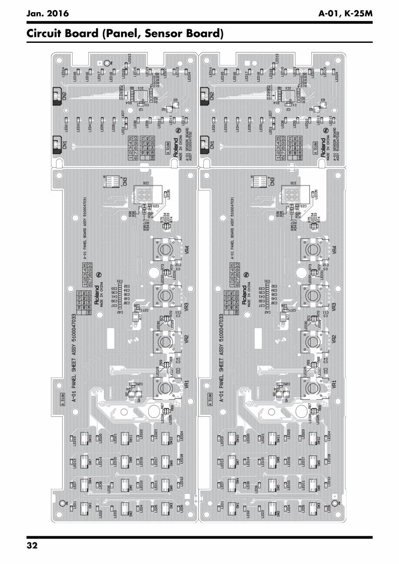
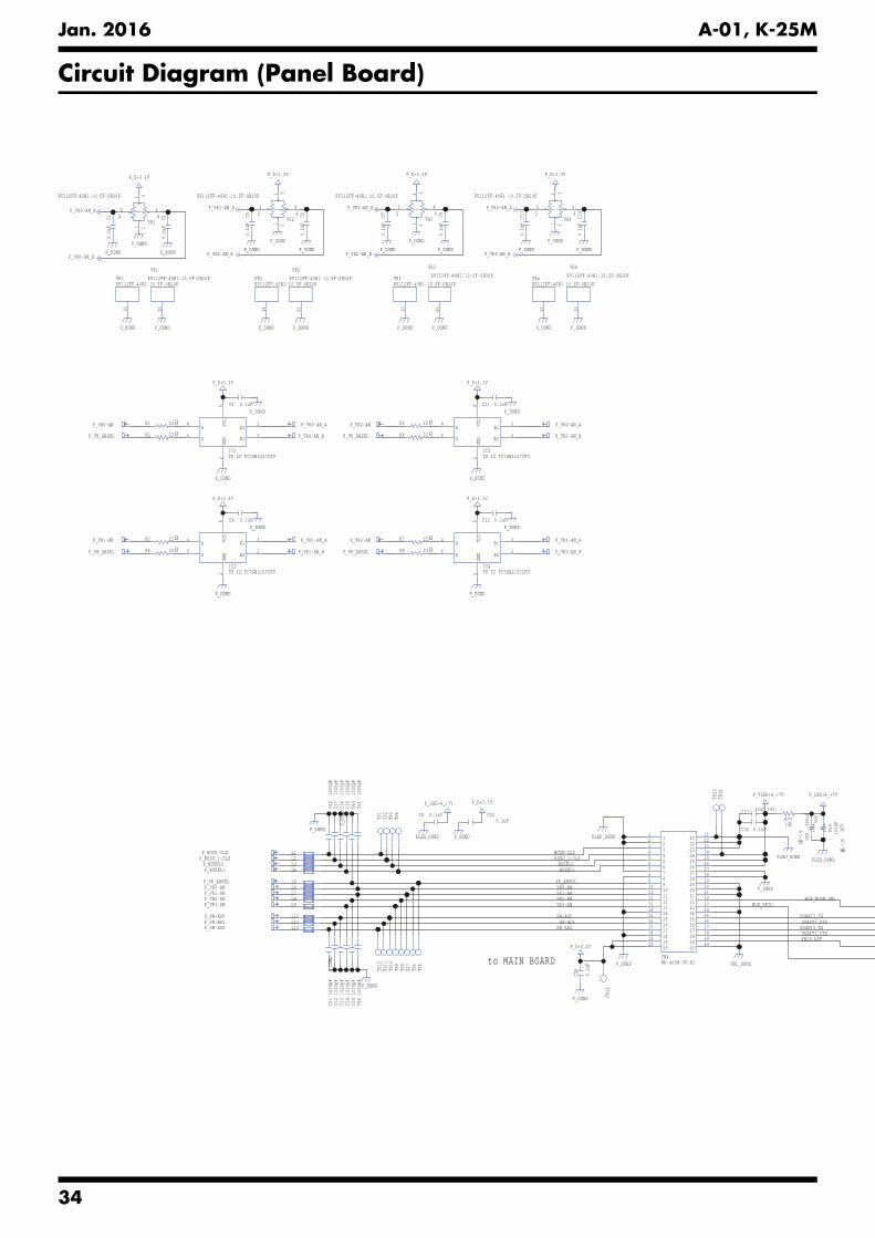
Circuit Board (Panel, Sensor Board)fig.b-panel-1.eps
32
Jan. 2016 A-01, K-25M
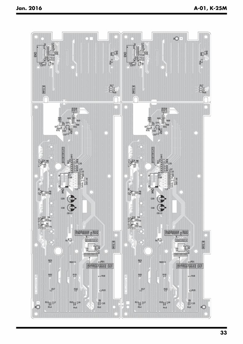
fig.b-panel-2.eps
33
Jan. 2016 A-01, K-25M
D
7V
EL
C30
100u
F16
V
Circuit Diagram (Panel Board)fig.d-panel.eps@L
P_DGND
P_DGND P_VR1-AN_B
P_DGND
P_VR1-ANP_VR0-AN
P_VR0-AN_B
P_VR1-AN_A
P_VR2-AN_B
P_DGND
P_VR3-AN_A
PLED_DGND
P_BUDO_1-CLK
P_DGND
P_LED+4_+7V
P_VR2-AN_A
P_BUSEL1
P_D+3.3V
P_DGND
P_DGND
P_BUSEL0
P_D+3.3V
P_DGND
P_D+3.3V
P_DGND
P_DGND
P_DGND
P_BUCK-CLK
P_D+3.3V
P_DGND
P_VR3-AN_B
P_VR_ABSEL
P_DGND
P_D+3.3V
P_D+3.3V
P_DGND
P_DGND
P_DGND
P_DGND
P_VR0-AN
P_VR2-AN_B
P_D+3.3V
P_VR1-AN
P_VR3-AN_B
P_SW-AD0
P_VR2-AN
P_VR0-AN_A
P_DGND
P_VR3-AN
P_DGND P_DGND P_DGND
P_DGND
P_D+3.3V
P_DGND
P_VR1-AN_A
P_VR0-AN_A
P_DGND
P_DGND
P_VR2-AN_A
P_VR2-AN
P_D+3.3V
P_VR3-AN
P_DGND
P_VR_ABSEL
P_DGND
P_VR_ABSEL
P_VR3-AN_A
P_VR1-AN_B
P_VR_ABSEL
P_DGND
P_VR_ABSEL
P_DGND
P_SW-AD1
P_VR0-AN_B
P_SW-AD2
P_D+3.3V
PLED_DGND
P_DGND
P_DGND
PLED_DGN
P_LED+4_+
P_DG
ND
P_DGND
SW-AD2SW-AD1
SW-AD0
VR3-ANVR2-ANVR1-AN
P_DG
ND
P_DGND
VR0-ANVR_ABSEL
BUSEL1BUSEL0
BUDO_1-CLKBUCK-CLK
P_DGND
BLE_MODE-SBLE_GPIO
USART3_TXUSART3_RTSUSART3_RXUSART3_CTSXBLE-RST
PBL_DGND
PLED_DGND
P_VLED+4_+7V
C29
100u
F
16V
22R8
22R2
22R4
22R5
22R6
22R1
22R3 22R7
1000
pFC3
2
1000
pFC3
510
00pF
C36
1000
pFC3
1
1000
pFC3
310
00pF
C34
1000
pFC4
2
1000
pFC4
010
00pF
C41
1000
pFC3
910
00pF
C38
1000
pFC3
7
L5
L2
L7L6
L11
L1
L9
L3L4
L8
L12
L10
16V10uFC27
0.1u
F
C28
0.1uFC11
0.1u
FC1
0.1uFC26
0.1u
FC5
0.1uFC8
0.1u
FC1
30.1uFC12
0.1u
FC6
0.1u
FC2
0.1u
FC9
0.1uFC10
0.1uFC3
0.1u
FC7
0.1u
FC1
4
0.1uFC4
TP IC TC7SB3157CFUIC3
4A
6S
2GN
D 1B2
3B1
5VC
C
TP IC TC7SB3157CFUIC4
4A
6S
2GN
D 1B2
3B1
5VC
C
TP IC TC7SB3157CFUIC1
4A
6S
2GN
D 1B2
3B1
5VC
C
TP IC TC7SB3157CFUIC2
4A
6S
2GN
D 1B2
3B1
5VC
C
RV112FF-40B1-10.5F-0B20KVR3
10
RV112FF-40B1-10.5F-0B20K
VR4
20
RV112FF-40B1-10.5F-0B20K
VR3
20
RV112FF-40B1-10.5F-0B20KVR2
10
RV112FF-40B1-10.5F-0B20KVR1
10
RV112FF-40B1-10.5F-0B20K
VR1
20
RV112FF-40B1-10.5F-0B20K
VR2
20
RV112FF-40B1-10.5F-0B20KVR4
10
RV112FF-40B1-10.5F-0B20K
VR3
22
1 1
44
3 3
RV112FF-40B1-10.5F-0B20K
VR1
22
1 1
44
3 3 RV112FF-40B1-10.5F-0B20K
VR2
22
1 1
44
3 3
RV112FF-40B1-10.5F-0B20K
VR4
22
1 1
44
3 3
TP12
TP11
TP10
TP9
TP8
TP6
TP5
TP4
TP3
TP2
TP1
TP7
TP20
TP21
TP22
WR-40PB-VF-N1CN4
3636
3535
3434
3333
3232
3131
3030
2929
2828
2727
2626
2525
2424
2323
2222
2121
11223344556677889910101111121213131414151516161717181819192020
4040
3939
3838
3737
1R77
to MAIN BOARD
34
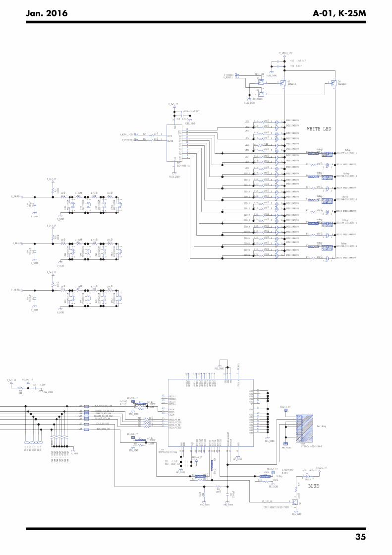
Jan. 2016 A-01, K-25M
P_SW-AD
P_SW-AD0
P_SW-AD2
P_D+3.3V
0R2
fig.d-panel.eps@R
USART3_RX_BB-CLKUSART3_RTS_BBUSART3_TX_BB-CLK
PBL_DGND
BLE_GPIO_BB
PBL_DGND
PBLD+3.3V
1
PBLD+3.3V
PBL_DGND
P_DGND
P_D+3.3V
BT_LED_ON
P_DGND
P_D+3.3V
PLED_DGND
P_DGND
PBLD+3.3V
PLED_DGND
PBLD+3.3V PBLD+3.3V
PBLD+3.3V
PBL_DGND
PLED_DGND
PBL_DGND
PBL_DGND
PBL_DGND
PBL_DGND
PBL_DGND
PBL_DGND
P_BUCK-CLK
P_BUDO_1-CLK
P_BUSEL0
PBL_DGND
P_D+3.3V
PLED_DGNDP_BUSEL1
P_DGND
P_DGND
P_DGND
P_LED+4_+7V
USART3_CTS_BB
XBLE_BB-RST
BLE_MODE-SEL_BB
P_DG
ND
P_DGND
PBLD+3.3V
P_D+3.3V
PBL_DGNDDTC114EUAT106(PB FREE)
Q31
23
10kR33
10kR32 UnPop
10kR65
10kR9
10kR10
10kR35
10kR64 UnPop
10kR11
10kR22
10kR34 UnPop
10kR23
10kR21
22R28
22R25
22R26
22R3122R3022R29
50V
1000
pFC1
6
1000
pFC4
9
1000
pFC2
3
1000
pFC4
4
1000
pFC4
7
50V
1000
pFC1
7
1000
pFC4
610
00pF
C45
1000
pFC4
3
50V
1000
pFC1
5
1000
pFC4
8
100R39
100R36
100R37
100
R38
1kR12
1kR14
1kR13
4.7kR20
4.7kR18
4.7kR19
2.2kR17
2.2kR16
2.2kR15
470R51
470R50
470R48
470R49
470R72UnPop
470R74UnPop
470R47
470R46
470R75
470R45
470R71
470R69
470R40
470R44
470R67
470R43
470R41
470R70UnPop
470R63
470R62
470R55
470R61
470R66UnPop
470R68UnPop
470R60
470R54
470R73470R59
470R53
470R58
470R57
470R56
470R42
470R52
RN1911FE
Q1
5
4 3
RN1911FE
Q1
2
1 6
L33
L37
L39
L38
L34
L36L35
BU2090FS-E2IC5
2DATA
3CLOCK
1VS
S 4Q0
5Q1
6Q2
7Q3
8Q4
9Q5
10Q6
11Q7
12Q8
13Q9
14Q10
15Q11
16VD
D
KRA225SQ42
31
KRA225SQ22
31
C22 10uF 16V
16V10uFC20
16V10uFC25
0.1uFC24
0.1uFC21
0.1uFC19
0.1uFC18
CN3FTSH-105-01-L-DV-K
33 22 11
44
99 88 77 66 55
1010
WW-GIS190TS-GLED25UnPop
1A
2K
WW-GIS190TS-GLED31UnPop
1A
2K
WW-GIS190TS-GLED33UnPop
1A
2K
WW-GIS190TS-GLED29UnPop
1A
2K
WW-GIS190TS-GLED27UnPop
1A
2K
IC6MBH7BLZ02-109004
VDD
28
18GPIO23
GPIO
2530
GPIO
2931
GPIO
2832
GND49
GPIO
835
GPIO
936
GPIO
1037
GPIO
1138
SWDI
O/nR
ESET
39SW
DCLK
40
GPIO
1212
GPIO
2713
GPIO
207
GPIO
168
GPIO
159
GPIO
1410
GPIO
1311
GND42
GND
41
GND
1
VDD1
.82
GND
3
GPIO
174
GPIO
195
GPIO
186
43GND
GND48
GND47
GND46
GND45
GND44
GPIO
734
GPIP
2614
GND
15
GPIO2116
GPIO2217
19GPIO24
GPIO620
GPIO521
GPIO422
33GP
IO30
GND
29
GPIO3/U_RX23
GPIO2/U_CTS24
GPIO1/U_TX25
GPIO0/U_RTS26
GND
27
GND50
NC51GND52GND53GND54GND55GND56
SMLE13WBC8WLED21 AK
SMLE13WBC8WLED10 AK
SMLE13WBC8WLED13 AK
SMLE13WBC8WLED23 AK
SMLE13WBC8WLED8 AK
SMLE13WBC8WLED341A
2K
SMLE13WBC8WLED321A
2K
SMLE13WBC8WLED301A
2K
SMLE13WBC8WLED281A
2K
SMLE13WBC8WLED261A
2K
SMLE13WBC8WLED24 AK
SMLE13WBC8WLED22 AK
SMLE13WBC8WLED3
AK
SMLE13WBC8WLED20 AK
SMLE13WBC8WLED6 AK
SMLE13WBC8WLED7 AK
SMLE13WBC8WLED18 AK
SMLE13WBC8WLED19 AK
SMLE13WBC8WLED1 AK
SMLE13WBC8WLED14 AK
SMLE13WBC8WLED17 AK
SMLE13WBC8WLED4 AK
SMLE13WBC8WLED15 AK
SMLE13WBC8WLED16 AK
SMLE13WBC8WLED11 AK
SMLE13WBC8WLED2 AK
SMLE13WBC8WLED9 AK
SMLE13WBC8WLED12 AK
SMLE13WBC8WLED5 AK
L-C191LBCT-ZX
LED35
1A
2K
EVQP
2202
MSW
12
312 4EV
QP22
02M
SW9
312 4
EVQP
2202
MSW
4
312 4
EVQP
2202
MSW
6
312 4EV
QP22
02M
SW3
312 4
EVQP
2202
MSW
11
312 4EV
QP22
02M
SW8
312 4EV
QP22
02M
SW5
312 4EV
QP22
02M
SW2
312 4
EVQP
2202
MSW
10
312 4EV
QP22
02M
SW7
312 4EV
QP22
02M
SW1
312 4
FS1
TP17
TP14
TP18
TP19
TP13
TP16
TP15
4
0R27
10k R78
220
R76
for dbug
L:UART/I2CH:SPI
L:UARTH:I2C
BLUE
WHITE LED
35

Jan. 2016 A-01, K-25M
Circuit Diagram (Sensor Board)fig.d-sensor.eps
SB_LED+4_+7V
SBLED_DGND
SBLED_DGND
SB_BUCK-CLK
SB_BUDO_0-CLK
SB_BUSEL0
SB_DRIVE_1-2
SBLED_DGND
SB_SENSE-2SB_DRIVE_2-2
SBLED_DGND
SB_BUSEL1
SBLED_DGND
SB_D+3.3V
SBLED_DGND
SBLED_DGND
SB_D+3.3V
SB_LED+4_+7VSB_DRIVE_1-1SB_DRIVE_2-1
SB_SENSE-1
SBLED_DGND
SBLED_DGND
SB_SENSE-2SB_DRIVE_2-2SB_DRIVE_1-2SB_SENSE-1
SB_DRIVE_2-1SB_DRIVE_1-1
SBLED_DGND
SB_BUDO_0-CLKSB_BUCK-CLK
SB_BUSEL0SB_BUSEL1
SBLED_DGND
50VCONNECTOR 52030-0429
CN1
1234
50VCONNECTOR 52030-0429
CN2
1234
22R2
22R1
220R5
220R10
220R6
220R12
220R9
220R4
220R7
220R11
220R8
470R14UnPop
220R13
RN1911FE
Q1
2
1 6
RN1911FE
Q1
5
4 3
BU2090FS-E2IC1
2DATA
3CLOCK
1VS
S 4Q0
5Q1
6Q2
7Q3
8Q4
9Q5
10Q6
11Q7
12Q8
13Q9
14Q10
15Q11
16VD
D
KRA225SQ32
31
KRA225SQ22
31
16V10uFC2
16V10uFC4
0.1uFC3
0.1uFC1
SMLE13WBC8WLED221A
2K
SMLE13WBC8WLED191A
2K
SMLE13WBC8WLED4 AK
SMLE13WBC8WLED241A
2K
SMLE13WBC8WLED3 AK SMLE13WBC8WLED151A
2K
SMLE13WBC8WLED12 AK
SMLE13WBC8WLED171A
2K
SMLE13WBC8WLED6 AK
SMLE13WBC8WLED9 AK
SMLE13WBC8WLED181A
2K
SMLE13WBC8WLED5 AK
SMLE13WBC8WLED11 AK
SMLE13WBC8WLED161A
2K
SMLE13WBC8WLED10 AK
SMLE13WBC8WLED141A
2K
SMLE13WBC8WLED7 AK
SMLE13WBC8WLED211A
2K
SMLE13WBC8WLED201A
2K
SMLE13WBC8WLED231A
2K
SMLE13WBC8WLED8 AK
WW-OR190TS-J(SQ) REDLED13UnPop
1A
2KWW-OR190TS-J(SQ)LED1
UnPopAK
0.1uFC5
0.1uF
C6
TP1TP2TP3TP4TP5
TP6TP7TP8TP9
TP10TP11TP12
TP13
CN3
20FLZ-SM2-TB (LF)(SN)
50V
1234567891011121314151617181920
33V
EZJZ
1V33
0GA
R15
1
2
33V
EZJZ
1V33
0GA
R16
1
2
33V
EZJZ
1V33
0GA
R17
1
2
33V
EZJZ
1V33
0GA
R18
1
2
33V
EZJZ
1V33
0GA
R19
1
2
33V
EZJZ
1V33
0GA
R20
1
2
SMLE13WBC8WLED2
1A
2K
1000
pFC7
UnPo
p10
00pF
C8Un
Pop
1000
pFC9
UnPo
p10
00pF
C10
UnPo
p10
00pF
C11
UnPo
p10
00pF
C12
UnPo
p
1000
pFC1
3Un
Pop
1000
pFC1
4Un
Pop
1000
pFC1
5Un
Pop
1000
pFC1
6Un
Pop
220R3
BEND/WHEEL
To MAIN BOARD
WHITE
36