sensing current and forces with spm - escholarship.org
TRANSCRIPT
Lawrence Berkeley National LaboratoryLawrence Berkeley National Laboratory
TitleSensing Current and Forces with SPM
Permalinkhttps://escholarship.org/uc/item/2zg6f17k
AuthorPark, Jeong Y.
Publication Date2010-08-31
eScholarship.org Powered by the California Digital LibraryUniversity of California
1
Sensing Current and Forces with SPM
Jeong Y. Park1,†
, Sabine Maier1, Bas Hendriksen
1, and Miquel Salmeron
1,2,*
1
Materials Sciences Division, Lawrence Berkeley National Laboratory, University of
California, Berkeley CA 94720
2 Materials Science and Engineering Department, University of California, Berkeley CA
94720
Abstract
Atomic force microscopy (AFM) and scanning tunneling microscopy (STM) are well
established techniques to image surfaces and to probe material properties at the atomic
and molecular scale. In this review, we show hybrid combinations of AFM and STM that
bring together the best of two worlds: the simultaneous detection of atomic scale forces
and conduction properties. We illustrate with several examples how the detection of
forces during STM and the detection of currents during AFM can give valuable
additional information of the nanoscale material properties.
*Authors to whom correspondence should be addressed. Electronic mail:
†Current address: WCU Program, Graduate School of EEWS, Korea Advanced Institute
of Science and Technology (KAIST), Daejeon, Republic of Korea.
2
I. Introduction
Did you ever touch a doorknob after walking on a carpet on a dry day? If you did
you probably sensed two properties in a single touch: the physical contact, i.e. the
doorknob is solid, and the unpleasant feeling of the electrical discharge, informing you
that the doorknob is a conductor. In this paper we review selected examples of such
combined mechanical and electrical sensing experiments at the atomic and molecular
scale using two branches of scanning probe microscopy (SPM), atomic force and
scanning tunneling microscopy.
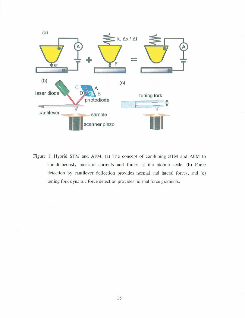
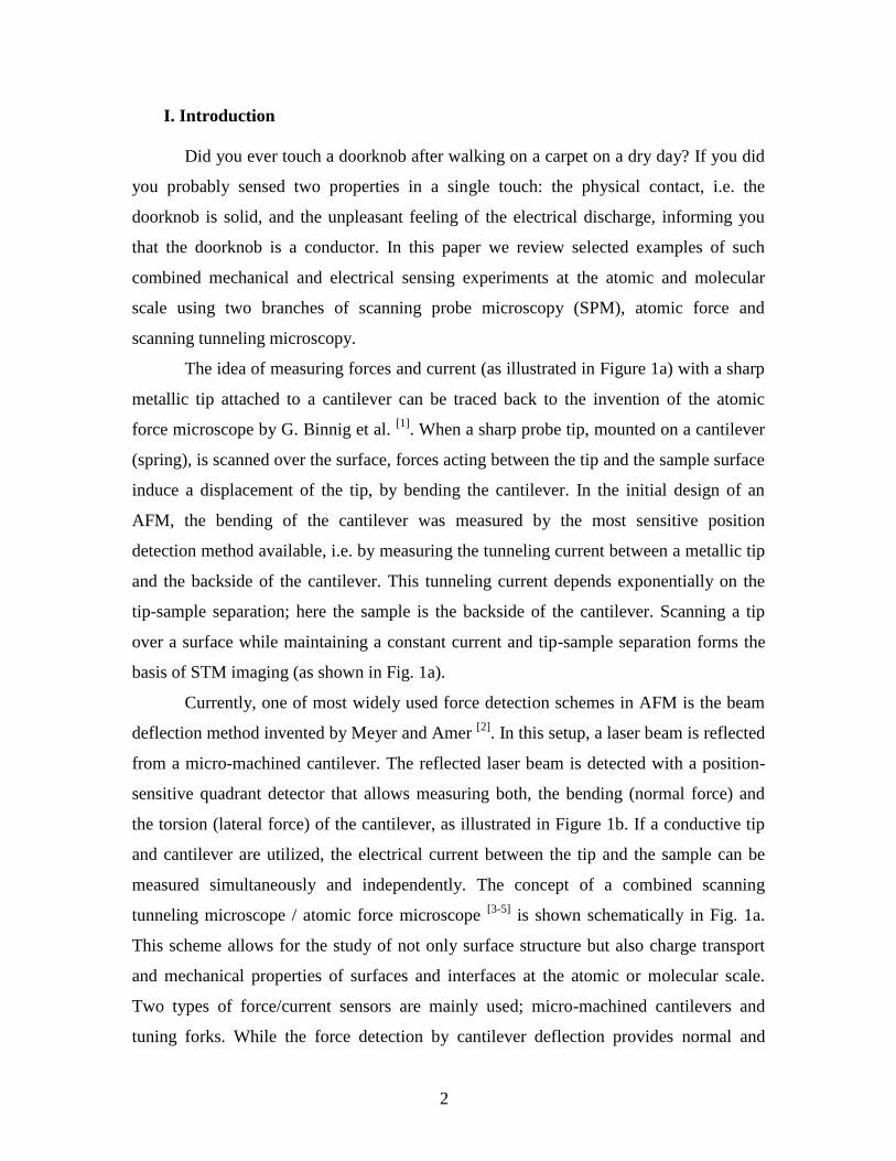
The idea of measuring forces and current (as illustrated in Figure 1a) with a sharp
metallic tip attached to a cantilever can be traced back to the invention of the atomic
force microscope by G. Binnig et al. [1]
. When a sharp probe tip, mounted on a cantilever
(spring), is scanned over the surface, forces acting between the tip and the sample surface
induce a displacement of the tip, by bending the cantilever. In the initial design of an
AFM, the bending of the cantilever was measured by the most sensitive position
detection method available, i.e. by measuring the tunneling current between a metallic tip
and the backside of the cantilever. This tunneling current depends exponentially on the
tip-sample separation; here the sample is the backside of the cantilever. Scanning a tip
over a surface while maintaining a constant current and tip-sample separation forms the
basis of STM imaging (as shown in Fig. 1a).
Currently, one of most widely used force detection schemes in AFM is the beam
deflection method invented by Meyer and Amer [2]
. In this setup, a laser beam is reflected
from a micro-machined cantilever. The reflected laser beam is detected with a position-
sensitive quadrant detector that allows measuring both, the bending (normal force) and
the torsion (lateral force) of the cantilever, as illustrated in Figure 1b. If a conductive tip
and cantilever are utilized, the electrical current between the tip and the sample can be
measured simultaneously and independently. The concept of a combined scanning
tunneling microscope / atomic force microscope [3-5]
is shown schematically in Fig. 1a.
This scheme allows for the study of not only surface structure but also charge transport
and mechanical properties of surfaces and interfaces at the atomic or molecular scale.
Two types of force/current sensors are mainly used; micro-machined cantilevers and
tuning forks. While the force detection by cantilever deflection provides normal and
3
lateral forces (Figure 1b), tuning fork force detection provides normal force gradients
(Figure 1c). Measurements of lateral forces with tuning forks require a different
mounting, as will be described later.
A combined AFM/STM can be operated in the static and dynamic modes,
depending on which feedback signal is used for tip-sample distance control. In the next
three sections, we will outline the different operation modes of combined AFM/STM and
some of their application in surface science.
II. Probing tip-surface forces in scanning tunneling microscopy
When one images surfaces with a heterogeneous electronic structure, variations of
tip-sample forces have a significant influence on the image contrast [3, 5]
. Understanding
the interaction between the STM tip and the substrate surface is therefore very important
for accurate image analysis and characterization of these electrically distinct regions,
such as semiconductor devices and organic molecules on metallic surfaces. Tip-sample
force interactions can be probed in STM mode by collecting the tunneling current with a
conducting AFM cantilever. While the tunneling current is used for the tip-sample
distance feedback control, the tip-sample force interaction is measured simultaneously by
monitoring the cantilever bending. To ensure stable tunneling,mode cantilevers or probes
with high spring constant (> 50 N/m) were used to suppress jump-to-contact instabilities.
Many efforts have been made to characterize tip-sample forces during scanning
tunneling microscopy. On metals and highly doped semiconductors the forces during
non-contact tunneling are attractive because the tip remains relatively far away from the
surface[6]
. Due to poor electrical conductivity in lightly doped semiconductors or in
insulating layers however, the tip might come very close to, or might even come in direct
contact with the surface, giving rise to a strong repulsive force [7, 8]
.
4
Initial investigations of the tip-surface interaction by measuring forces during
STM imaging focused on graphite, because its atomic lattice can be easily resolved in
air. Sugawara et al.[4]
observed repulsive forces indicative of contact and surface
conductance during STM/AFM imaging. Freshly etched tungsten and platinum levers
were used for sensing tip-surface forces in constant current STM mode. Similarly, the
forces acting between a Pt-Rh tip and graphite surface were studied by Mate et al.[9]
.
Grigg et al. measured such repulsive force between a W probe and Pt grating
surfaces in STM mode using a rocking beam force balance sensor [10]
and concluded that
surface contaminants repelled the probe from the underlying Pt It was observed that the
repulsive forces between probe and tip lead to elastic or inelastic deformations in the area
under the tip and therefore have important effects on imaging. Salmeron et al. reported
anomalous topographical corrugation (elastic deformation) and permanent damage
(inelastic deformation) during STM imaging of a graphite surface indicating the effect of
compressive and shear forces [11]
. Pi et al. observed irreversible deformation on the
alkylthiol self-assembled monolayers due to the repulsive tip-surface interaction [12]
.
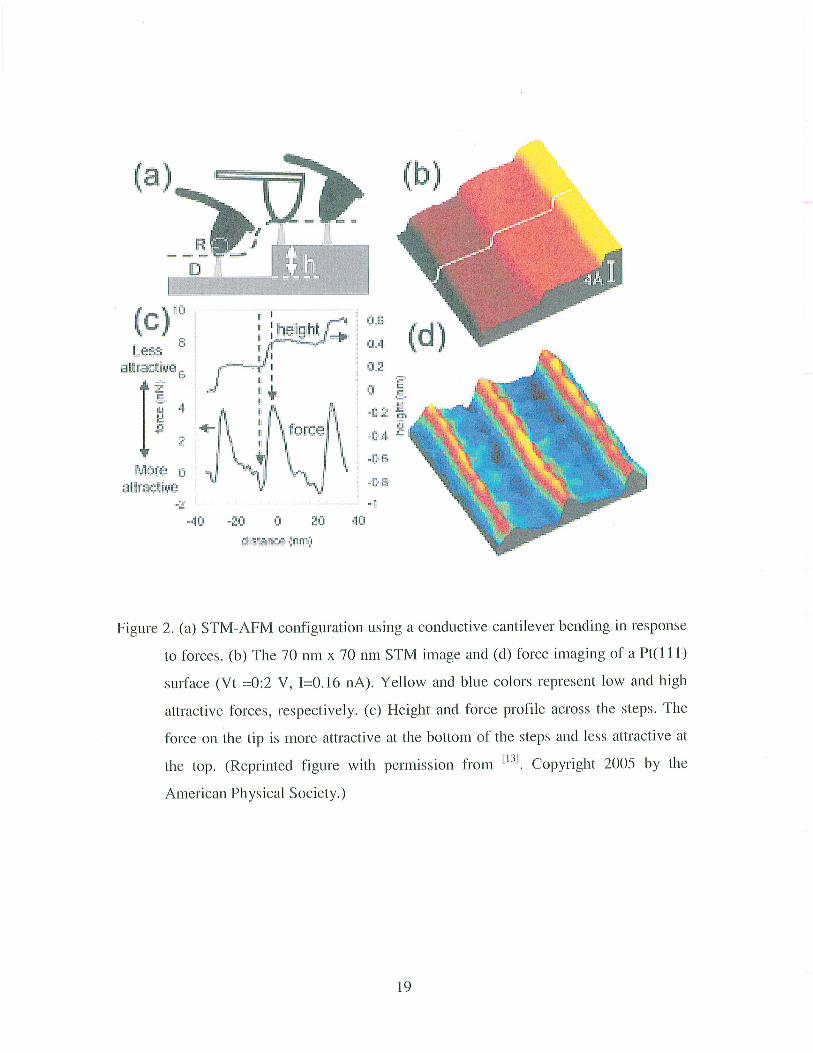
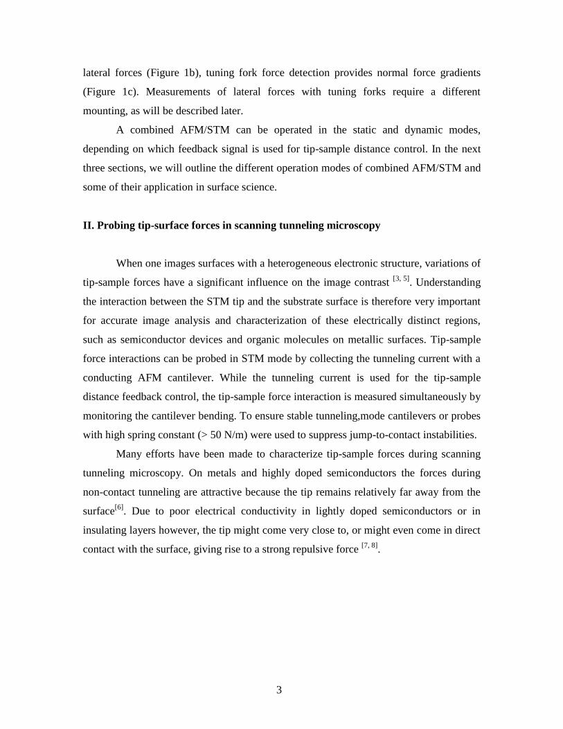
By simultaneous topographic and force measurements with a combined
STM/AFM, the strength of the electric field produced by dipoles at atomic steps was
measured on Pt(111), Au(111) and Al-Ni-Co quasicrystal surfaces as shown in the
scheme of Fig. 2a [13]
. Figures 2b and 2d show the STM topography and force image of
Pt(111) obtained simultaneously for a tip bias of –0.2 V and Fig. 2c the corresponding
height and force profiles . The force was always found to be attractive and increased by
~1.5 nN as the tip approached the bottom of the step and decreased by ~4 nN on the
upper terrace. When the attractive force increased, the STM current feedback loop
retracted the base of the cantilever to keep the tunnel current, and hence the tip-sample
distance, constant. The cantilever deflection provided a direct measurement of the forces
on the tip when crossing the step. The reduction of the attractive force in the upper side of
the steps was due to the reduction in the van der Waals and polarization part of the force
(image charges). This was a consequence of the fact that at the position of the step the
lower terrace is farther away from the tip. The contribution of the step dipole was
separated from changes in the force due to van der Waals and polarization forces by
varying the tip-sample bias.
5
It is well know that on electrically non-uniform surfaces, such as semiconductors,
variations of electrostatic forces during non-contact atomic force microscopy (AFM)
imaging lead to a strong bias dependence in topographical images [14]
. In STM imaging of
electrically heterogeneous surfaces similar effects exist. Force variations on a silicon pn
junction were investigated during STM imaging [8]
. It was found that in an attempt to
keep the tunneling current constant while crossing the pn junction on the n-area at reverse
bias the tip pressed against the surface to draw the set-point current, while it was in non-
contact tunneling regime at the forward bias on the p side of the junction.
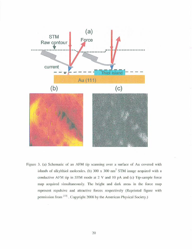
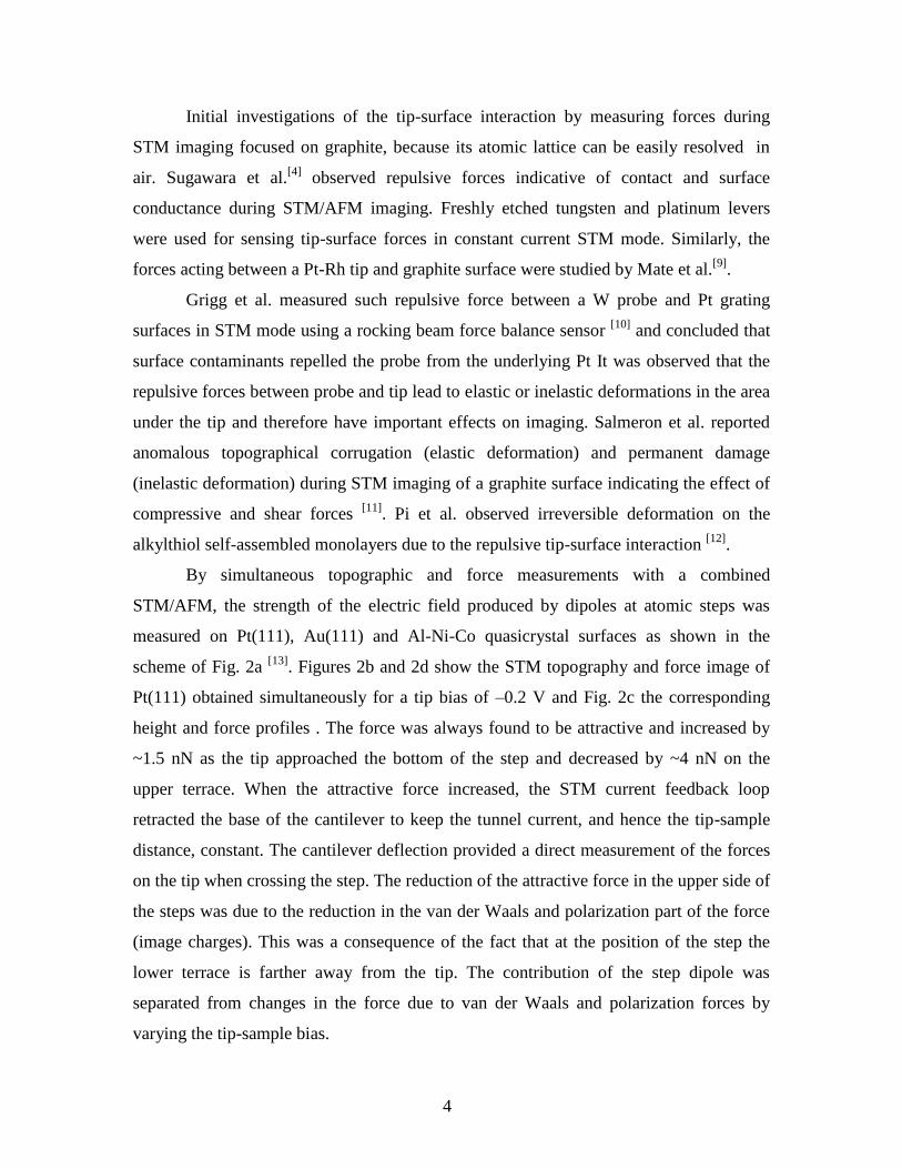
The mechanical interaction between a scanning tunneling microscopy probe and a
self-assembled monolayer of organic molecules was investigated by sensing the force
during STM imaging [15]
as shown in Figure 3. A Au(111) surface was partially covered
by hexadecane (C16) alkylthiol molecules forming islands. Figure 3a shows the
schematic of the STM tip scanning over the gold surface and the molecular islands, with
simultaneous force mapping. Depending on the current setpoint, the tip was in full
contact with the molecules, which produces a backward bending of the lever. Figures 3b
and 3c show STM and force images acquired simultaneously using a sample bias of 2 V
at a constant tunneling current of 10 pA. The dark circular areas in Fig. 3b represent 1 nm
deep depressions corresponding to the alkylthiol islands, with typical lateral dimensions
of 20–50 nm. The STM image is a plot of the variation of the length of the piezoactuator
supporting the sample during scanning. In normal STM operation, where the tip is rigid,
this produces a 'topographic' image, which is dominated by the reduced conductivity of
the islands and therefore does not represent true topography. In the present case,
however, the lever is bending due to variations in the normal force. A compensated STM
image with tip height profile can be obtained by compensating STM topography with
lever bending to reconstruct a topography image. In this manner it was found that the
interaction between the tip and the C16 alkylthiol molecules goes from non-contact to
contact at 1 pA at 2 V bias, which is comparable to the calculated threshold tunneling
current by Bumm et al [7]
.
III. Probing tip-surface currents in atomic force microscopy (static mode)
6
Conductive AFM (C-AFM) [16]
, another hybrid STM/AFM mode, is basically no
more than using electrically conductive AFM tips connected to a current pre-amplifier
during conventional contact-mode AFM, using the cantilever (normal) deflection as the
feedback signal to regulate the tip-substrate distance. When a bias voltage is applied
between the conducting tip and a conducting substrate one obtains the corresponding
current signal. The tip-sample current is an additional independent signal that allows for
conductance probing and mapping of samples with conducting and insulating areas or
domains. This makes C-AFM particularly useful to study electrically inhomogeneous
substrates. There are numerous studies using C-AFM and rather than providing a
complete review we briefly discuss a few examples and describe some experiments from
our own laboratory in more detail.
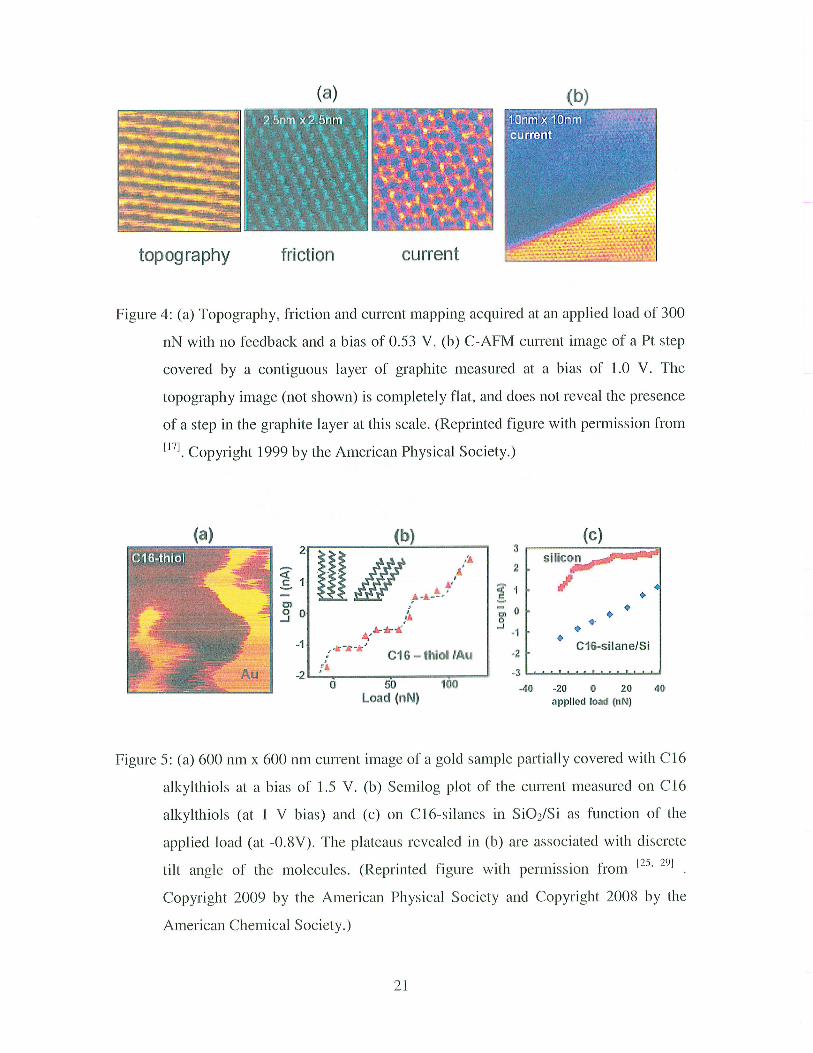
C-AFM can obtain lattice resolution. For example Enachescu at al. have used
tungsten carbide coated AFM tips to image the topography, friction and current on HOPG
and graphene layers on Pt (111) (See Figure 4a) [17]
. The current level was in the range of
nA-mA and revealed the lattice-resolved image of the carbon atoms. It was also shown
that the current level on the lower side of the step was reduced from 39 μA to 28 μA (see
Figure 4b) while the AFM topography is completely flat at the same area and does not
reveal the presence of a step in the graphite layer. The authors suggested that the high
resolution was due to the fact that only a small fraction of the tip-sample contact was
electrically conducting, much smaller than the physical contact area.
C-AFM [18 , 19]
and break-junction experiments [20, 21 , 22, 23]
are two of the tools for
studying the conduction properties of organic monolayers. In most tip-monolayer-
substrate junctions of C-AFM, the self-assembled monolayer (SAM) simply acts as a
tunneling barrier, albeit with a reduced barrier compared to a vacuum gap of the same
thickness. This is because the (tails of) HOMO-LUMO molecular levels assist electron
transfer by non-resonant tunneling through the molecular monolayer[24]
. External forces
that cause molecular deformation and conformation changes can influence charge
transport properties of conducting molecules. The capability of probing electrical and
mechanical properties with nanoscale resolution makes SPM a very useful and promising
tool in studying charge transport properties through molecules which, with adequate
theoretical support could provide invaluable information into molecular bonding
7
deformation mechanisms giving rise to changes in electronic levels and current. The field
of molecular electronics for example benefits enormously from the use of C-AFM to
measure local conductivity in organic films and its dependence on local molecular
structure and geometry, applied forces and the effect of gating bias voltages that change
the electronic level positions.
It was found that the electron tunneling process through alkylthiol self-assembled
monolayers on a gold substrate depends strongly on the tilt angle of the alkane chains [25-
27]. The tilt angle was varied by applying an increasing load by the tip on the SAM while
simultaneously measuring the tunnel current (see figure 5). It was suggested that when
the tilt angle increases electrons might tunnel not only along the backbone of the
molecules but also across neighboring molecules on their way from the tip to the
substrate [26]
. A similar 'two-pathway' tunneling model [28]
was found to be consistent
with the conduction through alkyl silane SAM [29]
. On the other hand, as pointed out for
alkylthiols on a gold substrate [25]
, distortions of the molecular bonds, particularly those
between the S end and Au, could also produce changes in the tunneling current when
tilting forces the S atom to change even slightly its position. Based on the load
dependence of the conduction through SAM of aromatic molecules, Fang et al. suggested
that intermolecular pi-orbital transport is involved in the tip-SAM-substrate conduction
[30]. Wold et al. have determined that the length dependence of the conduction through
conjugated oligophenylene SAMs is much weaker than through saturated alkane SAMs
[31]. The same was found by Sakaguchi et al.
[32]. Leatherman et al. studied the conduction
of conjugated carotene wires embedded in an alkanethiol SAM [33]
. More recently Choi et
al. used C-AFM to determine the resistance of long conjugated molecular wires and
found a transition of direct (nonresonant) tunneling to hopping transport through the
molecular wire depending on the length or the wire [34]
. By space charge limited current
measurements with C-AFM and modeling Reid et al. could extract reliable charge carrier
mobilities of various conjugated polymers [35]
. Cui et al. used gold nano particles to create
reliable contacts to alkanedithiols, which do not depend on the applied force. By scaling
and binning the obtained IV curves they could distinguish transport through single
molecule contacts [36]
. Photo-switching of the electrical conductance of azobenzene
derivatives was observed with C-AFM by Mativetsky [37]
. IV spectroscopy using C-AFM
8
is not limited to materials relevant to molecular/organic electronics. The IV
characteristics of biological molecules such as photosynthetic complexes and other
proteins have been studied as well [38-40]
.
Most C-AFM experiments described so far focused on the determination of the IV
characteristics. However, current imaging or mapping is also a very useful method to
determine spatial variations in the conductance. For example, Yang et al. found that the
structure and connectivity of pentacene layers strongly affects their lateral conduction [41]
.
Sutar et al. used C-AFM current mapping and IV spectroscopy to study the conduction
properties of polyaniline micro-crystalline heterostructures [42]
. Blends of organic
polymers (polyaniline and PMMA) have been studied by Planès et al. [43]
. Li et al.
imaged multi-walled carbon nanotubes that were vertically embedded in SiO2 by current
mapping [44]
.
Conductive AFM tips were used as a local probe electrode to contact molecular
islands of sexithiophene crystals and water polymerized polypyrol [45-47]
. The conduction
of a DNA network in contact with a gold electrodes has been imaged as a function of
humidity [48]
. Resistance mapping of carbon nanotubes in contact with an electrode has
been performed by several groups [49, 50]
. Paulson et al. pushed carbon nanotubes with the
AFM tip causing them to rotate in and out of registry with the lattice of the underlying
graphite substrate. Subsequent conduction measurements of the carbon nanotubes with
the C-AFM tip revealed that when the tube was commensurate with the graphite the
resistance was minimum[51]
. Nakamura et al. used a conducting AFM tip as the source
electrode to contact copper phthalocyanine nano-crystals in a field effect transistor (FET)
geometry [52]
. Yaish et al. used a Au coated AFM tip as a nanoprobe to measure the
resistance of a nanotube in a FET geometry [53]
. Seshadri and Frisbie used an Au coated
AFM tip to perform potentiometry of an operating sexithiophene based FET [54]
.
The use of C-AFM is obviously not limited to organic materials. The electrical
properties of a variety of inorganic materials have been studied with C-AFM. Examples
include ultrathin layers of SiO2 [55-57]
, TiO2 [58]
polycrytalline ZnO [59]
, ZnO nano rods
[60], Cr films on SiC
[61], Au nanostructures
[62] GaMnAs structures
[63], CdTe nano-
tetrapods [64]
, etc. In addition to the use of C-AFM for local electrical probing the tip can
9
be used for nanopatterning. Electrical fields and currents applied by the C-AFM tip have
been used to locally oxidize structures [65, 66]
, to write patterns in SAM [67]
or to inject
charges locally, to anchor nanoparticles, i.e., the nanoscale equivalent of the Xerox
process [68]
.
In the examples given above the conducting AFM was only used as a local
electrical probe. Recent work by Chang et al. is an example that truly exploits the
combined force and current detection [69]
. These researchers detected the attractive forces
between pairs of guanine-cytosine and adenine-thymine molecules, one molecule of the
pair adsorbed on the tip and the other one in a SAM on the substrate. The molecules of
the pair interacted through hydrogen bonds and the tunneling current was measured
through those hydrogen bonds by C-AFM. The authors used the C-AFM force and
current data to construct an electromechanical model describing the role of stiffness of
the (STM)-(molecule)-(hydrogen bond)-(molecule)-(substrate) junction in their separate
STM-based transport measurements for molecular recognition.
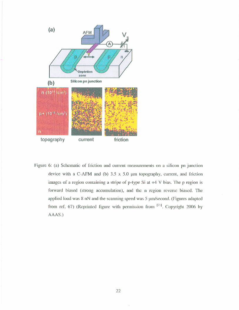
Contact-mode AFM is a powerful tool to study the nanoscale friction properties of
materials (friction force microscopy, FFM) [70]
. When conducting tips are used in AFM
friction experiments the effect of electronic components of friction can be studied. An
example of such effects is illustrated by the recent report of the electronic friction
properties of planar silicon pn junctions [71]
. In this study a conducting TiN AFM tip was
scanned over a planar pn junction covered with a thin oxide layer. There was no
noticeable difference in the friction between the p-type and the n-type area of the silicon
substrate at zero sample bias. However when a positive sample voltage was applied the
friction on the p-type area was higher compared to the n-type area (see Figure 6). At
positive sample voltage the p-type area was in forward bias, i.e. holes accumulated in the
area under the tip, and the n-type area was in reverse bias, i.e. electrons were depleted.
Although the current was higher on the forward-biased p-type area it was found that the
friction was actually independent of the current value between the tip and the sample. In a
separate study Qi et al. found a similar electronic effect on n-type GaAs covered with an
ultrathin oxide [72]
. An asymmetry was found in the friction force while scanning the
GaAs at forward bias and reverse bias. Consistent with the Si pn junctions the friction
was found to be higher at forward bias. A charge trapping model was suggested to
10
explain the observed magnitude of the friction force, its bias dependence, and the
scanning velocity dependence. According to this model, charges get trapped in the oxide
covering the GaAs only in forward bias leaving a slowly decaying trail of charges behind
the tip that exert an electrostatic pull on the tip that is manifested as an increases in the
friction force.
The electromechanical properties of ferroelectric materials are widely studied
with piezoresponsive force microscopy (PFM) [73]
. In PFM, a conductive AFM tip is used
to apply an AC voltage to the ferroelectric material. The resulting piezoresponse of the
ferroelectric, i.e. the mechanical response to the applied voltage, is detected in the lateral
force signal, i.e. the torsional response of the AFM cantilever. In this way domains of
different piezoelectric polarization orientation can be resolved. By applying a sufficiently
high DC voltage the orientation of the domains can be switched reversibly and patterns
can be written. Recently, Seidel et al. have shown by C-AFM that the domain walls
separating piezoelectric domains in BiFeO3 films are electrically conductive, whereas the
domains themselves are insulating [74]
.
The reliability of C-AFM measurements strongly depends on the quality of the C-
AFM tips and various conducting coatings including Pt, Au, TiN and W2C have been
evaluated [75-78]
. It is generally found that AFM tips coated with metal films fail after
some time of use because the metal coating wears off. Fein et al. used tapping mode
AFM with a conductive tip to measure the current during the short time of contact [79]
.
Operating C-AFM in tapping mode reduces the shear forces on the tip, which allowed the
tips to last longer. On the other hand, inspection of Pt-coated silicon tips used in our lab
for current imaging revealed the formation of a thin film of organic molecules that caused
reduction of the conductivity of the AFM tip. Reliable C-AFM imaging on the hard
sample surface requires the coating of hard materials on the tip because the soft coating
materials can be easily peeled off upon contact with the hard material. If the hardness of
tip coating material is much higher than that of sample surface, it results in plastic
deformation or scratching on the sample surface. Therefore, the choice of materials for
the tip coating would be a key factor of reliable operation of C-AFM.
11
IV. Probing tip-surface currents in atomic force microscopy (dynamic mode)
The combination of force and current sensing has been successfully extended to
dynamic non-contact AFM/STM. By using metal-coated or highly-doped silicon
cantilevers, the current has been monitored during frequency modulated (FM) and
amplitude modulated (AM) noncontact AFM on conductive samples. In FM-AFM, this
operation mode has been used to better understand the imaging contrast on surfaces at the
atomic level. For example Enevoldsen et al. modeled the tip structure during the imaging
of a TiO2(110) surface in combination with atomistic STM simulations based on multiple
scattering theory [80]
. Inversely, in dynamic STM a time averaged tunnel current between
the conducting sample and the oscillating tip can be used to control the probe height
above the sample surface. This method combines the high lateral resolution achieved by
STM with complementary data on the force gradient. Atomic resolution has been
achieved on several conductive samples, such as Si(111)-(7x7) [81, 82]
and Cu [83]
as well as
molecular resolution on organic molecules [84, 85]
.
Further, using the tunneling current as control parameter for the distance to the
sample while simultaneously oscillating the tip parallel to the surface makes it possible to
determine lateral forces [86, 87]
However, achieving atomic resolution is difficult due to the
large oscillation amplitudes (over tens of nm) required using microfabricated cantilevers.
Nonetheless, the attraction and repulsion at a monatomic step could be quantified, as well
as the force between sulfur impurities and the tip on a Cu(001) surface [86]
. The use of
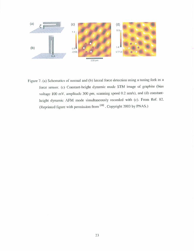
quartz tuning forks as force sensors enables FM-AFM operation with amplitudes of
several Angstroms. In this manner true atomic resolution on a Si(111)-(7x7) surface has
been established by showing that both conservative and dissipative force components
exhibit clear variations on the atomic scale as shown in Fig. 7a and 7b [87]
.
At a temperature of 4K thermal drift rates are small and allow simultaneous high-
resolution measurements of tunneling current and frequency shift at constant tip-sample
distance. In these operating conditions quartz tuning forks are common sensors and can
provide enhanced sensitivity to short-range forces. In this way, Hembacher et al. studied
the atomic structure of a graphite (0001) surface in great detail. Combined STM/AFM
experiments using the frequency modulation force microscopy method, with the
cantilever oscillating at fixed amplitude revealed the 'hidden' atoms in the unit cell [88, 89]
.
12
Figure 7c and 7d show constant-height dynamic mode STM image and constant-height
dynamic AFM image, respectively, which reveal two types of atoms forming the basis of
the hexagonal surface unit cell, (white) and (red). While only the atoms appear in
the STM image (Figure 7c), dynamic mode AFM image (Figure 7d) shows both and
atoms.
Recently, the forces required to pull individual adsorbates along a surface have
been quantified using the same technique [90]
. Ternes et al. have shown that moving single
cobalt (Co) atoms on Pt(111) require a lateral force of 210 pN, independent of the vertical
force, while about 17 pN were sufficient to manipulate Co atoms on Cu(111). These
results clearly show that the required force to move an atom strongly depends on the
supporting substrate.
V. Conclusion and outlook
In this review, several examples of hybrid AFM and STM measurements have
been presented that illustrate how this combination can give valuable electronic structure
information in addition to the topographical imaging. Scanning tunneling microscopy
provides higher lateral resolution than contact atomic force microscopy. Hence, using
STM as feedback, while additionally recording forces, is an ideal combination when high
resolution and stability is required. Conducting atomic force microscopy (C-AFM) has
been used to analyze the electrical properties of a variety of nano-objects, from single
molecules, organic films, to nanowires. Simultaneous detection of mechanical properties
like friction can lead to understand the correlation between molecular deformation and
charge transport. Recently, more functionality has been added to the hybrid combinations
of AFM and STM. For example, simultaneous laser irradiation extends conventional
conductive atomic force microscopy to photo conductive AFM [91]
to measure
photoconductance with nanoscale resolution.
Acknowledgements
This work was supported by the Director, Office of Science, Office of Basic
Energy Sciences, Materials Sciences and Engineering Division, of the U.S. Department
13
of Energy under Contract No. DE-AC02-05CH11231. J.Y.P. acknowledges the partial
support by WCU (World Class University) program through the National Research
Foundation of Korea funded by the Ministry of Education, Science and Technology (31-
2008-000-10055-0).
14
References
[1] G. Binnig, C. F. Quate and C. Gerber, Physical Review Letters 1986, 56, 930-933.
[2] G. Meyer and N. M. Amer, Applied Physics Letters 1988, 53, 1045-1047.
[3] D. Anselmetti, A. Baratoff, H. J. Guntherodt, C. Gerber, B. Michel and H. Rohrer, J.
Vac. Sci. Technol. B 1994, 12, 1677-1680.
[4] Y. Sugawara, T. Ishizaka and S. Morita, J. Vac. Sci. Technol. B 1991, 9, 1092-1095
[5] S. L. Tang, J. Bokor and R. H. Storz, Applied Physics Letters 1988, 52, 188-190.
[6] U. Durig, J. K. Gimzewski and D. W. Pohl, Physical Review Letters 1986, 57, 2403-
2406.
[7] L. A. Bumm, J. J. Arnold, T. D. Dunbar, D. L. Allara and P. S. Weiss, Journal of
Physical Chemistry B 1999, 103, 8122-8127.
[8] J. Y. Park, R. J. Phaneuf, D. F. Ogletree and M. Salmeron, Applied Physics Letters
2005, 86, 172105.
[9] C. M. Mate, R. Erlandsson, G. M. McClelland and S. Chiang, Surface Science 1989,
208, 473-486.
[10] D. A. Grigg, P. E. Russell and J. E. Griffith, J. Vac. Sci. Technol. A 1992, 10, 680-
683
[11] M. Salmeron, D. F. Ogletree, C. Ocal, H. C. Wang, G. Neubauer, W. Kolbe and G.
Meyers, J. Vac. Sci. Technol. B 1991, 9, 1347-1352
[12] U. H. Pi, M. S. Jeong, J. H. Kim, H. Y. Yu, C. W. Park, H. Lee and S. Y. Choi,
Surface Science 2005, 583, 88-93.
[13] J. Y. Park, G. M. Sacha, M. Enachescu, D. F. Ogletree, R. A. Ribeiro, P. C.
Canfield, C. J. Jenks, P. A. Thiel, J. J. Saenz and M. Salmeron, Physical Review Letters
2005, 95, 136802.
[14] S. Sadewasser and M. C. Lux-Steiner, Physical Review Letters 2003, 91, 266101.
[15] J. Y. Park, Y. B. Qi, I. Ratera and M. Salmeron, Journal of Chemical Physics 2008,
128, 234701.
[16] Various names for this mode exist depending on authors and AFM manufacturers:
conduction AFM (C-AFM), current-sensing AFM (CS-AFM), conducting-probe AFM
(CP-AFM), tunneling AFM (TUNA), scanning spreading resistance microscopy (SSRM).
[17] M. Enachescu, D. Schleef, D. F. Ogletree and M. Salmeron, Physical Review B
1999, 60, 16913-16919.
[18] M. Salmeron, G. Neubauer, A. Folch, M. Tomitori, D. F. Ogletree and P. Sautet,
Langmuir 1993, 9, 3600-3611.
[19] D. L. Klein and P. L. McEuen, Applied Physics Letters 1995, 66, 2478-2480.
[20] M. A. Reed, C. Zhou, C. J. Muller, T. P. Burgin and J. M. Tour, Science 1997, 278,
252-254.
[21] C. Kergueris, J. P. Bourgoin, S. Palacin, D. Esteve, C. Urbina, M. Magoga and C.
Joachim, Physical Review B 1999, 59, 12505-12513.
[22] B. Q. Xu and N. J. J. Tao, Science 2003, 301, 1221-1223.
[23] P. Reddy, S. Y. Jang, R. A. Segalman and A. Majumdar, Science 2007, 315, 1568-
1571.
[24] W. Y. Wang, T. Lee and M. A. Reed, Reports on Progress in Physics 2005, 68, 523-
544.
15
[25] Y. B. Qi, I. Ratera, J. Y. Park, P. D. Ashby, S. Y. Quek, J. B. Neaton and M.
Salmeron, Langmuir 2008, 24, 2219-2223.
[26] H. Song, H. Lee and T. Lee, Journal of the American Chemical Society 2007, 129,
3806.
[27] D. J. Wold and C. D. Frisbie, Journal of the American Chemical Society 2001, 123,
5549-5556.
[28] K. Slowinski, R. V. Chamberlain, C. J. Miller and M. Majda, Journal of the
American Chemical Society 1997, 119, 11910-11919.
[29] J. Y. Park, Y. B. Qi, P. D. Ashby, B. L. M. Hendriksen and M. Salmeron, Journal of
Chemical Physics 2009, 130, 114705.
[30] L. Fang, J. Y. Park, H. Ma, A. K. Y. Jen and M. Salmeron, Langmuir 2007, 23,
11522-11525.
[31] D. J. Wold, R. Haag, M. A. Rampi and C. D. Frisbie, Journal of Physical Chemistry
B 2002, 106, 2813-2816.
[32] H. Sakaguchi, A. Hirai, F. Iwata, A. Sasaki, T. Nagamura, E. Kawata and S.
Nakabayashi, Applied Physics Letters 2001, 79, 3708-3710.
[33] G. Leatherman, E. N. Durantini, D. Gust, T. A. Moore, A. L. Moore, S. Stone, Z.
Zhou, P. Rez, Y. Z. Liu and S. M. Lindsay, Journal of Physical Chemistry B 1999, 103,
4006-4010.
[34] S. H. Choi, B. Kim and C. D. Frisbie, Science 2008, 320, 1482-1486.
[35] O. G. Reid, K. Munechika and D. S. Ginger, Nano Letters 2008, 8, 1602-1609.
[36] X. D. Cui, A. Primak, X. Zarate, J. Tomfohr, O. F. Sankey, A. L. Moore, T. A.
Moore, D. Gust, G. Harris and S. M. Lindsay, Science 2001, 294, 571-574.
[37] J. M. Mativetsky, G. Pace, M. Elbing, M. A. Rampi, M. Mayor and P. Samori,
Journal of the American Chemical Society 2008, 130, 9192.
[38] A. Stamouli, J. W. M. Frenken, T. H. Oosterkamp, R. J. Cogdell and T. J. Aartsma,
Febs Letters 2004, 560, 109-114.
[39] D. G. Xu, G. D. Watt, J. N. Harb and R. C. Davis, Nano Letters 2005, 5, 571-577.
[40] J. W. Zhao, J. J. Davis, M. S. P. Sansom and A. Hung, Journal of the American
Chemical Society 2004, 126, 5601-5609.
[41] H. C. Yang, T. J. Shin, M. M. Ling, K. Cho, C. Y. Ryu and Z. N. Bao, Journal of the
American Chemical Society 2005, 127, 11542-11543.
[42] D. S. Sutar, S. Lenfant, D. Vuillaume and P. Yakhmi, Organic Electronics 2008, 9,
602-608.
[43] J. Planes, F. Houze, P. Chretien and O. Schneegans, Applied Physics Letters 2001,
79, 2993-2995.
[44] J. Li, R. Stevens, L. Delzeit, H. T. Ng, A. Cassell, J. Han and M. Meyyappan,
Applied Physics Letters 2002, 81, 910-912.
[45] T. W. Kelley, E. L. Granstrom and C. D. Frisbie, Advanced Materials 1999, 11, 261.
[46] M. J. Loiacono, E. L. Granstrom and C. D. Frisbie, Journal of Physical Chemistry B
1998, 102, 1679-1688.
[47] S. I. Yamamoto and K. Ogawa, Surface Science 2006, 600, 4294-4300.
[48] A. Terawaki, Y. Otsuka, H. Y. Lee, T. Matsumoto, H. Tanaka and T. Kawai,
Applied Physics Letters 2005, 86, 113901.
[49] H. J. Dai, E. W. Wong and C. M. Lieber, Science 1996, 272, 523-526.
16
[50] Y. Otsuka, Y. Naitoh, T. Matsumoto and T. Kawai, Applied Physics Letters 2003,
82, 1944-1946.
[51] S. Paulson, A. Helser, M. B. Nardelli, R. M. Taylor, M. Falvo, R. Superfine and S.
Washburn, Science 2000, 290, 1742-1744.
[52] M. Nakamura, H. Yanagisawa, S. Kuratani, M. Iizuka and K. Kudo, Thin Solid
Films 2003, 438, 360-364.
[53] Y. Yaish, J. Y. Park, S. Rosenblatt, V. Sazonova, M. Brink and P. L. McEuen,
Physical Review Letters 2004, 92, 046401.
[54] K. Seshadri and C. D. Frisbie, Applied Physics Letters 2001, 78, 993-995.
[55] W. Frammelsberger, G. Benstetter, J. Kiely and R. Stamp, Applied Surface Science
2006, 252, 2375-2388.
[56] A. Olbrich, B. Ebersberger and C. Boit, Applied Physics Letters 1998, 73, 3114-
3116.
[57] S. J. O'Shea, R. M. Atta, M. P. Murrell and M. E. Welland, Journal of Vacuum
Science & Technology B 1995, 13, 1945-1952.
[58] C. J. Boxley, H. S. White, C. E. Gardner and J. V. Macpherson, Journal of Physical
Chemistry B 2003, 107, 9677-9680.
[59] R. Shao, S. V. Kalinin and D. A. Bonnell, Applied Physics Letters 2003, 82, 1869-
1871.
[60] E. Schlenker, A. Bakin, B. Postels, A. C. Mofor, H. H. Wehmann, T. Weimann, P.
Hinze and A. Waag, Physica Status Solidi B-Basic Solid State Physics 2007, 244, 1473-
1477.
[61] P. Mazur, S. Zuber, M. Grodzicki and A. Ciszewski, Vacuum 2007, 82, 364-371.
[62] A. Bietsch, M. A. Schneider, M. E. Welland and B. Michel, Journal of Vacuum
Science & Technology B 2000, 18, 1160-1170.
[63] R. Farshchi, P. D. Ashby, D. J. Hwang, C. P. Grigoropoulos, R. V. Chopdekar, Y.
Suzuki and O. D. Dubon, Physica B-Condensed Matter 2007, 401, 447-450.
[64] L. Fang, J. Y. Park, Y. Cui, P. Alivisatos, J. Shcrier, B. Lee, L. W. Wang and M.
Salmeron, Journal of Chemical Physics 2007, 127, 184704.
[65] E. S. Snow and P. M. Campbell, Science 1995, 270, 1639-1641.
[66] K. Wilder, C. F. Quate, D. Adderton, R. Bernstein and V. Elings, Applied Physics
Letters 1998, 73, 2527-2529.
[67] S. Kramer, R. R. Fuierer and C. B. Gorman, Chemical Reviews 2003, 103, 4367-
4418.
[68] L. Seemann, A. Stemmer and N. Naujoks, Nano Letters 2007, 7, 3007-3012.
[69] S. Chang, J. He, A. Kibel, M. Lee, O. Sankey, P. Zhang and S. Lindsay, Nature
Nanotechnology 2009, 4, 297-301.
[70] R. W. Carpick and M. Salmeron, Chemical Reviews 1997, 97, 1163-1194.
[71] J. Y. Park, D. F. Ogletree, P. A. Thiel and M. Salmeron, Science 2006, 313, 186-
186.
[72] Y. B. Qi, J. Y. Park, B. L. M. Hendriksen, D. F. Ogletree and M. Salmeron, Physical
Review B 2008, 77, 184105.
[73] S. V. Kalinin, A. Rar and S. Jesse, Ieee Transactions on Ultrasonics Ferroelectrics
and Frequency Control 2006, 53, 2226-2252.
[74] J. Seidel, L. W. Martin, Q. He, Q. Zhan, Y. H. Chu, A. Rother, M. E. Hawkridge, P.
Maksymovych, P. Yu, M. Gajek, N. Balke, S. V. Kalinin, S. Gemming, F. Wang, G.
17
Catalan, J. F. Scott, N. A. Spaldin, J. Orenstein and R. Ramesh, Nature Materials 2009,
8, 229-234.
[75] S. J. O'Shea, R. M. Atta and M. E. Welland, Review of Scientific Instruments 1995,
66, 2508-2512.
[76] T. Trenkler, T. Hantschel, R. Stephenson, P. De Wolf, W. Vandervorst, L.
Hellemans, A. Malave, D. Buchel, E. Oesterschulze, W. Kulisch, P. Niedermann, T.
Sulzbach and O. Ohlsson, Journal of Vacuum Science & Technology B 2000, 18, 418-
427.
[77] J. Y. Park, Y. B. Qi, D. F. Ogletree, P. A. Thiel and M. Salmeron, Physical Review B
2007, 76.
[78] M. Enachescu, R. W. Carpick, D. F. Ogletree and M. Salmeron, Journal of Applied
Physics 2004, 95, 7694-7700.
[79] A. Fein, Y. M. Zhao, C. A. Peterson, G. E. Jabbour and D. Sarid, Applied Physics
Letters 2001, 79, 3935-3937.
[80] G. H. Enevoldsen, H. P. Pinto, A. S. Foster, M. C. R. Jensen, A. Kühnle, M.
Reichling, W. A. Hofer, J. V. Lauritsen and F. Besensbacher, Physical Review B 2008,
78, 045416.
[81] P. Güthner, J. Vac. Sci. Technol. B 1996, 14, 2428-2431.
[82] R. Lüthi, E. Meyer, M. Bammerlin, A. Baratoff, T. Lehmann, L. Howald, C. Gerber
and Güntherodt, Z. Phys. B 1996, 100, 165-167.
[83] C. Loppacher, M. Bammerlin, M. Guggisberg, S. Schar, R. Bennewitz, A. Baratoff,
E. Meyer and H. J. Guntherodt, Physical Review B 2000, 62, 16944-16949.
[84] N. Berdunov, A. J. Pollard and P. H. Beton, Applied Physics Letters 2009, 94,
043110.
[85] C. Loppacher, M. Bammerlin, M. Guggisberg, E. Meyer, H. J. Güntherodt, R. Lüthi,
R. Schlittler and J. K. Gimzewski, Appl. Phys. A 2001, 72, S105-S108.
[86] O. Pfeiffer, R. Bennewitz, A. Baratoff, E. Meyer and P. Grutter, Physical Review B
2002, 65, 161403.
[87] F. J. Giessibl, M. Herz and J. Mannhart, PNAS 2002, 99, 12006-12010.
[88] S. Hembacher, F. J. Giessibl, J. Mannhart and C. F. Quate, PNAS 2003, 100, 12539-
12542.
[89] S. Hembacher, F. J. Giessibl, J. Mannhart and C. F. Quate, Physical Review Letters
2005, 94, 056101.
[90] M. Ternes, C. P. Lutz, C. F. Hirjibehedin, F. J. Giessibl and A. J. Heinrich, Science
2008, 319, 1066-1069.
[91] J. Lee, I. Choi, S. Hong, S. Lee, Y. I. Yang, Y. Kim and J. Yi, Ultramicroscopy
2008, 108, 1090-1093.