robust penetrating microelectrodes for neural interfaces realized by titanium micromachining
TRANSCRIPT
Robust penetrating microelectrodes for neural interfacesrealized by titanium micromachining
Patrick T. McCarthy & Kevin J. Otto & Masaru P. Rao
Published online: 1 March 2011# The Author(s) 2011. This article is published with open access at Springerlink.com
Abstract Neural prosthetic interfaces based upon penetrat-ing microelectrode devices have broadened our understand-ing of the brain and have shown promise for restoringneurological functions lost to disease, stroke, or injury.However, the eventual viability of such devices for use inthe treatment of neurological dysfunction may be ultimatelyconstrained by the intrinsic brittleness of silicon, thematerial most commonly used for manufacture of penetrat-ing microelectrodes. This brittleness creates predispositionfor catastrophic fracture, which may adversely affect thereliability and safety of such devices, due to potential forfragmentation within the brain. Herein, we report thedevelopment of titanium-based penetrating microelectrodesthat seek to address this potential future limitation.Titanium provides advantage relative to silicon due to itssuperior fracture toughness, which affords potential forcreation of robust devices that are resistant to catastrophic
failure. Realization of these devices is enabled by recentlydeveloped techniques which provide opportunity for fabri-cation of high-aspect-ratio micromechanical structures inbulk titanium substrates. Details are presented regarding thedesign, fabrication, mechanical testing, in vitro functionalcharacterization, and preliminary in vivo testing of devicesintended for acute recording in rat auditory cortex andthalamus, both independently and simultaneously.
Keywords MEMS . Prosthesis . Electrophysiology .
Recording .Microstimulation . Brain-machine
1 Introduction
Penetrating microelectrode devices, which allow direct andselective recording and stimulation of neural tissues, haveprovided unprecedented opportunity for enhancing under-standing of neurophysiological processes underlying manyaspects of human function and behavior (Bak et al. 1990,Gelbard-Sagiv et al. 2008). They have also shown immensepromise for restoring neurological functions lost to disease,stroke, or injury (Normann 2007), as exemplified by neuralprostheses that have enabled restoration of rudimentaryauditory perception (Otto et al. 2008, Otto, Rousche andKipke 2005a, Otto, Rousche and Kipke 2005b) and controlof assistive instrumentation for those with motor dysfunc-tion (Hochberg et al. 2006). However, this technology isstill in its formative stages and many challenges remain.
While the improvement of chronic recording reliabilityremains a key near-term challenge for this emergingtechnology (Vetter et al. 2004), its eventual maturation intoa clinically viable technique for restoring lost neurologicalfunction will also require development of devices that arecapable of withstanding surgical manipulation by neuro-
P. T. McCarthySchool of Mechanical Engineering, Birck Nanotechnology Center,Purdue University,West Lafayette, IN 47907, USA
K. J. OttoSchool of Biological Sciences and the Weldon School ofBiomedical Engineering, Purdue University,West Lafayette, IN 47907, USA
M. P. RaoSchool of Mechanical Engineering, Birck Nanotechnology Center,Purdue University,West Lafayette, IN 47907, USA
M. P. Rao (*)Department of Mechanical Engineering,University of California-Riverside,A313 Bourns Hall,Riverside, CA 92521, USAe-mail: [email protected]
Biomed Microdevices (2011) 13:503–515DOI 10.1007/s10544-011-9519-5
surgeons (Kipke et al. 2008), and are immune to safetyhazards associated with fracture-based fragmentation. Theintrinsic brittleness of silicon, the material most commonlyused for the manufacture of such devices, may ultimatelyprove limiting in this regard. This brittleness, which arisesfrom the low fracture toughness of silicon, creates non-negligible probability for catastrophic failure by fracture.This has not been a significant concern in the evolution ofthis technology thus far. However, the potential for devicefragmentation within the brain, no matter how small,coupled with the potentially severe consequences associat-ed with such fragmentation in future clinical settings,suggests need for consideration of means for addressingthis potential concern.
In addition to potential safety concerns, propensity forfracture of silicon-based microelectrodes may also adverse-ly affect reliability, since fracture often results in completeloss of device functionality. It also places practicalconstraint on many current silicon devices with regard tothe device length that can be reliably inserted, since risk ofbuckling-related fracture increases with device length,while opportunity for increasing buckling resistancethrough increased shank cross section area is constrainedby potential adverse affects associated with increasedinsertion damage (Szarowski et al. 2003, Seymour andKipke 2007). In many animal models, this practical lengthlimitation hampers access to sub-cortical structures andlargely precludes extension towards simultaneous recordingwithin precisely-defined cortical and sub-cortical regions.This latter capability is of particular interest, since it mayserve as a critical enabler for enhancing understanding ofimportant neural processing networks, such as the cortico-thalamic loops that underlie auditory, visual, and somato-sensory processing (Nicolelis et al. 1995, Fanselow andNicolelis 1999, Sherman and Guillery 2002, Winer andLarue 1987, Hubel and N. 1972, Nicolelis and Shuler2001). This, therefore, provides additional impetus todevelop penetrating microelectrode devices with greaterrobustness.
Alternative microelectrode materials systems that havebeen explored include those based on ceramics (Moxon etal. 2004b), polymers (Lee et al. 2004a, Schuettler et al.2005, Stieglitz et al. 2000, Rousche et al. 2001), and metals(Motta and Judy 2005, Fofonoff et al. 2004). Ceramicsoffer only limited benefit relative to silicon, with regard toreliability and safety, since they suffer from similar orgreater propensity for fracture (Ward et al. 2009). Recentlyreported microelectrodes based on polycrystalline diamondshow potential for realization of highly flexible, thin crosssection devices with sufficient stiffness for cortical pene-tration (Chan et al. 2009). However, low signal to noiseratio observed during neural recording indicates need forfurther device refinement. Polymers used thus far possess
sufficient toughness to mitigate fracture. However, theirlow elastic moduli typically require trade-off betweendevice stiffness and functional reliability, since relativelylarge cross section areas are required to ensure insertionreliability and recording site placement accuracy (Lee et al.2004b, Suzuki, Mabuchi and Takeuchi 2003, Takeuchi etal. 2004), which increases insertion damage. A number ofstrategies have been proposed to circumvent this trade-off,including those based on stiffening through incorporationof dissolvable rigid polymer coatings (Suzuki et al. 2003)or internal reinforcements (Lee et al. 2004b, Takeuchi et al.2005, Takeuchi et al. 2004).
Metals show particular promise for use in microelectrodeapplications due to their high fracture toughness, whichensures graceful failure via plastic deformation, rather thancatastrophic fracture (i.e. devices will bend before theybreak). This increases safety by minimizing potential forfragmentation, and may also enhance reliability, sincepotential exists for maintaining device functionality despiteoverloading. Moreover, when coupled with the moderate tohigh moduli of metals, this enables realization of robustmicroelectrodes with small cross section areas, thusfacilitating insertion and reducing injury. However, despitethese advantageous characteristics, metallic microelectrodesreported to-date suffer from limitations that may constraintheir ultimate safety or utility. For example, in the devicesdemonstrated by Motta and Judy (Motta and Judy 2005),gold coatings were implemented to prevent exposure of theunderlying nickel structural backbone to the physiologicalenvironment. This may adversely affect safety, due topotential for cytotoxic Ni ion release in the event of coatingfailure. In the devices demonstrated by Fofonoff et al.(Fofonoff et al. 2004), toxicity concerns were largelyalleviated through the use of titanium as a structuralbackbone. However, opportunity for probing sequentiallyinterconnected neural processing networks with suchdevices is constrained by reliance upon the Utah ElectrodeArray geometry, which consists of arrayed electrodes withonly single, tip-located recording sites.
We have recently reported preliminary results from thedevelopment of titanium-based penetrating microelectrodesthat seek to address the above-mentioned limitations(McCarthy et al. 2009). Realization of these devices wasfundamentally enabled by recently developed techniquesthat allow, for the first time, fabrication of high-aspect-ratiomicromechanical devices within bulk titanium substrates(Aimi et al. 2004, Parker et al. 2005). Herein, we expandupon this report to detail the design, fabrication, mechanicaltesting, and in vitro functional characterization of titanium-based microelectrode devices intended for use in acute ratauditory cortex and thalamus recording, both independentlyand simultaneously. Results from acute in vivo character-ization of these devices are also briefly touched upon, but
504 Biomed Microdevices (2011) 13:503–515
are more fully elaborated elsewhere (McCarthy, Rao andOtto 2011).
2 Design and fabrication
2.1 Design
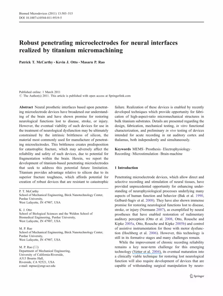
The microelectrodes produced in this effort were designedto study auditory cortex and thalamus responses within a ratmodel, both individually and simultaneously. As such, shortdevices (2 mm shank length) were designed for acutecortical recording, and longer devices (4.9 & 5.4 mm shanklengths) were designed for acute thalamic recording,independently of, or in conjunction with cortex. Bothdevice types were modeled after commercially-available“Michigan” type electrode arrays (A1×16–5 mm 100–413,NeuroNexus Technologies, Ann Arbor, MI; Shank length =5 mm, shank thickness ~ 15 μm, shank width = 33–200 μm(distal & proximal ends of shank, respectively), recordingsite diameter = 23 μm, & recording site pitch = 100 μm).Each titanium device contained 16 independently address-able circular recording sites, and 18 distinct design variantswere developed with differing shank length (2, 4.9, &5.4 mm), recording site diameter (23 & 40 μm), and pitch(50, 75, 100, & 150 μm). Since optimal designs for theintended applications have yet to be defined, the givenvariation of these parameters was reflective of the desire toeventually determine the most favorable combination thatensures consistent sampling of discrete neurons within thetargeted neural regions with high signal to noise ratio.
Figures 1 and 2 show schematic representations of devicedesign variants for acute auditory cortical and corticothalamicrecording, respectively. In all devices, recording sites wereconnected by 5 μm wide traces (with 9 μm pitch) to remote100 μm×100 μm contact pads (with 150 μm pitch) arrayedat the proximal end of the device. In devices with 23 μmdiameter recording sites, this resulted in shanks with widththat tapered from 48 μm at the recording site closest to thedistal end of the shank (i.e. near the sharp tip) to 192 μm atthe base. In the 40 μm diameter recording site devices, shankwidth ranged from 65 to 209 μm. Devices intended forcortical recording were designed with 16 recording sitesarrayed from the distal end of the shank. Devices intendedfor corticothalamic recording were designed with one set of8 recording sites arrayed within the vicinity of 2 mm fromthe proximal end of the shank, and an additional set of8 recording sites arrayed from the distal end of the shank.
2.2 Fabrication
The titanium-based microelectrode devices were fabricatedfrom 25.4±7.62 μm thick Ti foil substrates (Gr 1 Ti,
99.7% Ti, Fine Metals Corp, Ashland, VA). The as-received foils were first solvent cleaned by ultrasonicagitation in acetone and isopropanol, respectively, fol-lowed by DI rinsing and N2 drying. Next, as shown inFig. 3, the first 0.6 μm SiO2 dielectric layer was depositedby plasma-enhanced chemical vapor deposition (PECVD)to insulate the subsequent electrical structures from thesubstrate (Benchmark 800 CVD, Axic Inc, Santa Clara,CA; Process conditions SiO2: 230 mT chamber pressure,26 W RF power, 200 sccm N2O, 35 sccm 5% SiH4, and300°C lower electrode temperature). The substrates werethen subjected to solvent cleaning, and mounted to 100 mmSi carrier wafers with thermally conductive adhesive tape(9882, 3M Electronics, St. Paul, MN). Recording sites,traces, and contact pads were then patterned via standardphotolithographic liftoff techniques with electron beamdepositions of 20 nm Ti/500 nm Au (CHA SE-600, CHAIndustries, Fremont, CA; Process conditions: 1.0×10⁻⁶ Tbase pressure and 1Å/s deposition rate).
Following metal deposition, the samples were soaked inacetone to release the Ti foils from the carrier wafer andthen solvent cleaned. The second dielectric layer, composedof 0.2 μm Si3N4 followed by 0.8 μm of SiO2, was thendeposited by PECVD to provide insulation from thesurrounding environment (Benchmark 800 CVD, Process
Fig. 1 Schematic representation of a typical titanium microelectrodedevice designed for acute cortical recording in rat
Biomed Microdevices (2011) 13:503–515 505

conditions Si3N4: 400 mT chamber pressure, 100 W RFpower, 100 sccm NH3, 120 sccm 5% SiH4, and 300°Clower electrode temperature). This dual layer stack waschosen to promote adhesion to the underlying Au patternsand minimize stress-induced curvature of the devicesarising from intrinsic stresses and thermal expansionmismatch between the deposited film and the underlyingTi substrate.
After completion of the second dielectric layer deposi-tion, the Ti foils were again mounted to 100 mm carrierwafers with thermally conductive tape. The contact andrecording site windows were then opened via photolitho-
graphic patterning and dry etching of the second dielectriclayer (E620 R&D, Panasonic Factory Solutions, Japan;Process conditions: 7.5 mT chamber pressure, 500 W ICPsource power, 400 W substrate RF power, and 40.0 sccmCHF3). The photoresist was then stripped and the sampleswere soaked in acetone to release the Ti foils from thecarriers.
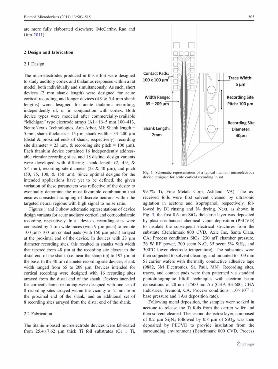
The third dielectric layer, composed of 0.2 μm Si3N4 and3.00 μm SiO2, was then deposited by PECVD to serve as anetch mask for the subsequent deep etch of the underlying Tisubstrate. The samples were re-mounted to carrier wafers,and the shank profiles were patterned and transferred into thedielectric layers via dry etching (E620 R&D, Processconditions: 1.9 mT chamber pressure, 900 W ICP sourcepower, 200 W substrate RF power, and 40.0 sccm CHF3).The photoresist was then stripped and the shank profileswere transferred through the underlying Ti substrate usingthe titanium inductively coupled plasma deep etch (TIDE)process (E620 R&D, Process conditions: 15 mT chamberpressure, 400 W ICP source power, 100 W substrate RFpower, 100 sccm Cl2, and 5 sccm Ar) (Parker et al. 2005).The samples were then subjected to a final short dry etch toremove the remaining thin dielectric layer protecting thecontact pads and recording sites, and released from thecarrier by soaking in acetone. Scanning electron micrographsof a typical completed device are shown in Fig. 4. Thesmooth vertical sidewalls resulting from the TIDE processare clearly evident, as is the integrity of the dielectric andmetal layers deposited on the titanium substrate.
Fig. 3 Fabrication process flow for titanium microelectrodes
Fig. 2 Schematic representation of a typical titanium microelectrodedevice designed for acute auditory corticothalamic loop recording inrat
506 Biomed Microdevices (2011) 13:503–515
2.3 Packaging
The microelectrode devices were packaged by bonding tocommercially-available printed circuit boards (PCBs) (A-16, NeuroNexus Technologies) using cyanoacrylate adhe-sive (Pacer Technology, Rancho Cucamonga, CA). Goldwire-bonding was then used to make connections betweenthe contact pads on the devices and their respective bondpads on the PCBs (7400A, West-Bond, Anaheim, CA).Afterwards, an additional layer of cyanoacrylate wasapplied over the contact pad area as an encapsulant toprotect the exposed wires.
2.4 In situ recording site cleaning
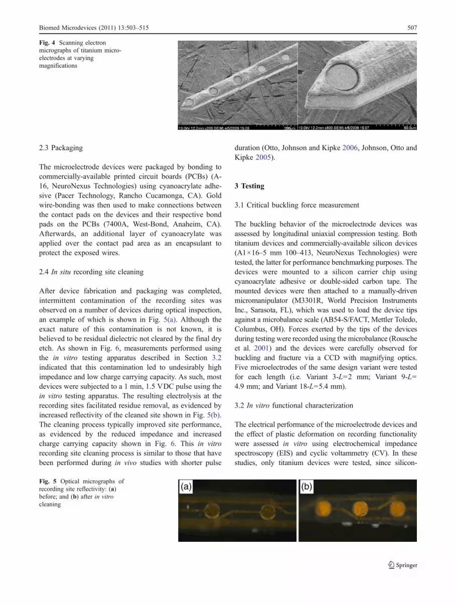
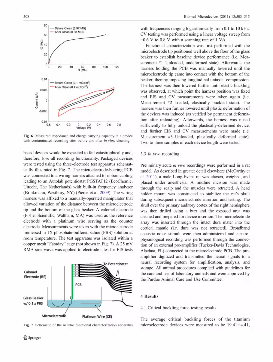
After device fabrication and packaging was completed,intermittent contamination of the recording sites wasobserved on a number of devices during optical inspection,an example of which is shown in Fig. 5(a). Although theexact nature of this contamination is not known, it isbelieved to be residual dielectric not cleared by the final dryetch. As shown in Fig. 6, measurements performed usingthe in vitro testing apparatus described in Section 3.2indicated that this contamination led to undesirably highimpedance and low charge carrying capacity. As such, mostdevices were subjected to a 1 min, 1.5 VDC pulse using thein vitro testing apparatus. The resulting electrolysis at therecording sites facilitated residue removal, as evidenced byincreased reflectivity of the cleaned site shown in Fig. 5(b).The cleaning process typically improved site performance,as evidenced by the reduced impedance and increasedcharge carrying capacity shown in Fig. 6. This in vitrorecording site cleaning process is similar to those that havebeen performed during in vivo studies with shorter pulse
duration (Otto, Johnson and Kipke 2006, Johnson, Otto andKipke 2005).
3 Testing
3.1 Critical buckling force measurement
The buckling behavior of the microelectrode devices wasassessed by longitudinal uniaxial compression testing. Bothtitanium devices and commercially-available silicon devices(A1×16–5 mm 100–413, NeuroNexus Technologies) weretested, the latter for performance benchmarking purposes. Thedevices were mounted to a silicon carrier chip usingcyanoacrylate adhesive or double-sided carbon tape. Themounted devices were then attached to a manually-drivenmicromanipulator (M3301R, World Precision InstrumentsInc., Sarasota, FL), which was used to load the device tipsagainst a microbalance scale (AB54-S/FACT, Mettler Toledo,Columbus, OH). Forces exerted by the tips of the devicesduring testing were recorded using the microbalance (Rouscheet al. 2001) and the devices were carefully observed forbuckling and fracture via a CCD with magnifying optics.Five microelectrodes of the same design variant were testedfor each length (i.e. Variant 3-L=2 mm; Variant 9-L=4.9 mm; and Variant 18-L=5.4 mm).
3.2 In vitro functional characterization
The electrical performance of the microelectrode devices andthe effect of plastic deformation on recording functionalitywere assessed in vitro using electrochemical impedancespectroscopy (EIS) and cyclic voltammetry (CV). In thesestudies, only titanium devices were tested, since silicon-
Fig. 4 Scanning electronmicrographs of titanium micro-electrodes at varyingmagnifications
(a) (b)Fig. 5 Optical micrographs ofrecording site reflectivity: (a)before; and (b) after in vitrocleaning
Biomed Microdevices (2011) 13:503–515 507
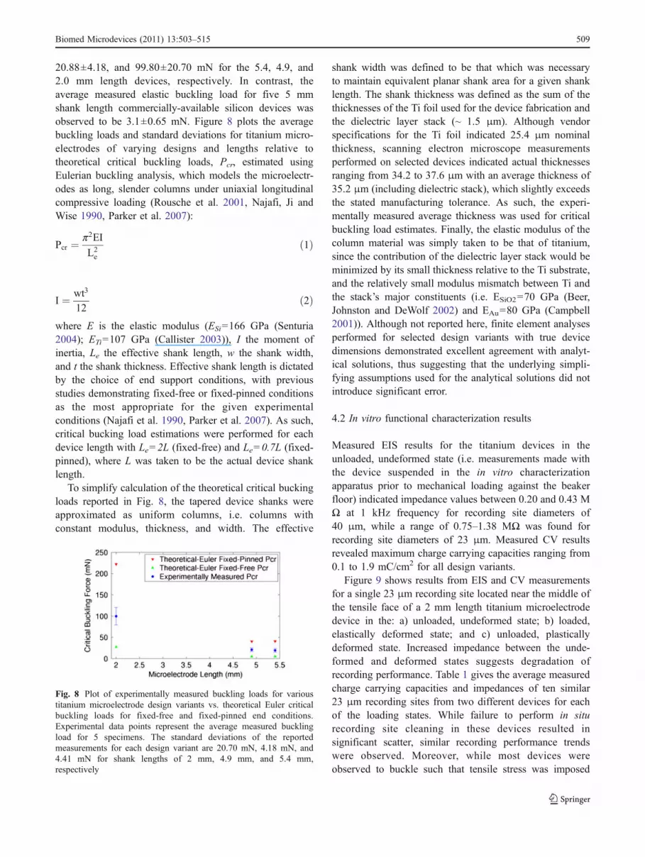
based devices would be expected to fail catastrophically and,therefore, lose all recording functionality. Packaged deviceswere tested using the three-electrode test apparatus schemat-ically illustrated in Fig. 7. The microelectrode-bearing PCBwas connected to a wiring harness attached to ribbon cablingleading to an Autolab potentiostat PGSTAT12 (EcoChemie,Utrecht, The Netherlands) with built-in frequency analyzer(Brinkmann, Westbury, NY) (Pierce et al. 2009). The wiringharness was affixed to a manually-operated manipulator thatallowed variation of the distance between the microelectrodetip and the bottom of the glass beaker. A calomel electrode(Fisher Scientific, Waltham, MA) was used as the referenceelectrode with a platinum wire serving as the counterelectrode. Measurements were taken with the microelectrodeimmersed in 1X phosphate-buffered saline (PBS) solution atroom temperature. The test apparatus was isolated within acopper mesh “Faraday” cage (not shown in Fig. 7). A 25 mVRMA sine wave was applied to electrode sites for EIS tests
with frequencies ranging logarithmically from 0.1 to 10 kHz.CV testing was performed using a linear voltage sweep from−0.6 V to 0.8 V with a scanning rate of 1 V/s.
Functional characterization was first performed with themicroelectrode tip positioned well above the floor of the glassbeaker to establish baseline device performance (i.e. Mea-surement #1–Unloaded, undeformed state). Afterwards, theharness holding the PCB was manually lowered until themicroelectrode tip came into contact with the bottom of thebeaker, thereby imposing longitudinal uniaxial compression.The harness was then lowered further until elastic bucklingwas observed, at which point the harness position was fixedand EIS and CV measurements were taken again (i.e.Measurement #2–Loaded, elastically buckled state). Theharness was then further lowered until plastic deformation ofthe devices was induced (as verified by permanent deforma-tion after unloading). Afterwards, the harness was raisedsufficiently to fully unload the plastically-deformed device,and further EIS and CV measurements were made (i.e.Measurement #3–Unloaded, plastically deformed state).Two to three samples of each device length were tested.
3.3 In vivo recording
Preliminary acute in vivo recordings were performed in a ratmodel. As described in greater detail elsewhere (McCarthy etal. 2011), a male Long-Evans rat was chosen, weighed, andplaced under anesthesia. A midline incision was madethrough the scalp and the muscles were retracted. A headholder mount was constructed to stabilize the rat’s skullduring subsequent microelectrode insertion and testing. Theskull over the primary auditory cortex of the right hemispherewas then drilled using a burr and the exposed area wascleaned and prepared for device insertion. The microelectrodearray was inserted through the intact dura mater into thecortical mantle (i.e. dura was not retracted). Broadbandacoustic noise stimuli were then administered and electro-physiological recording was performed through the connec-tion of an external pre-amplifier (Tucker-Davis Technologies,Alachua, FL) connected to the microelectrode PCB. The pre-amplifier digitized and transmitted the neural signals to aneural recording system for amplification, analysis, andstorage. All animal procedures complied with guidelines forthe care and use of laboratory animals and were approved bythe Purdue Animal Care and Use Committee.
4 Results
4.1 Critical buckling force testing results
The average critical buckling forces of the titaniummicroelectrode devices were measured to be 19.41±4.41,Fig. 7 Schematic of the in vitro functional characterization apparatus
Fig. 6 Measured impedance and charge carrying capacity in a devicewith contaminated recording sites before and after in vitro cleaning
508 Biomed Microdevices (2011) 13:503–515
20.88±4.18, and 99.80±20.70 mN for the 5.4, 4.9, and2.0 mm length devices, respectively. In contrast, theaverage measured elastic buckling load for five 5 mmshank length commercially-available silicon devices wasobserved to be 3.1±0.65 mN. Figure 8 plots the averagebuckling loads and standard deviations for titanium micro-electrodes of varying designs and lengths relative totheoretical critical buckling loads, Pcr, estimated usingEulerian buckling analysis, which models the microelectr-odes as long, slender columns under uniaxial longitudinalcompressive loading (Rousche et al. 2001, Najafi, Ji andWise 1990, Parker et al. 2007):
Pcr ¼ p2EI
L2e
ð1Þ
I ¼ wt3
12ð2Þ
where E is the elastic modulus (ESi=166 GPa (Senturia2004); ETi=107 GPa (Callister 2003)), I the moment ofinertia, Le the effective shank length, w the shank width,and t the shank thickness. Effective shank length is dictatedby the choice of end support conditions, with previousstudies demonstrating fixed-free or fixed-pinned conditionsas the most appropriate for the given experimentalconditions (Najafi et al. 1990, Parker et al. 2007). As such,critical bucking load estimations were performed for eachdevice length with Le=2L (fixed-free) and Le=0.7L (fixed-pinned), where L was taken to be the actual device shanklength.
To simplify calculation of the theoretical critical buckingloads reported in Fig. 8, the tapered device shanks wereapproximated as uniform columns, i.e. columns withconstant modulus, thickness, and width. The effective
shank width was defined to be that which was necessaryto maintain equivalent planar shank area for a given shanklength. The shank thickness was defined as the sum of thethicknesses of the Ti foil used for the device fabrication andthe dielectric layer stack (~ 1.5 μm). Although vendorspecifications for the Ti foil indicated 25.4 μm nominalthickness, scanning electron microscope measurementsperformed on selected devices indicated actual thicknessesranging from 34.2 to 37.6 μm with an average thickness of35.2 μm (including dielectric stack), which slightly exceedsthe stated manufacturing tolerance. As such, the experi-mentally measured average thickness was used for criticalbuckling load estimates. Finally, the elastic modulus of thecolumn material was simply taken to be that of titanium,since the contribution of the dielectric layer stack would beminimized by its small thickness relative to the Ti substrate,and the relatively small modulus mismatch between Ti andthe stack’s major constituents (i.e. ESiO2=70 GPa (Beer,Johnston and DeWolf 2002) and EAu=80 GPa (Campbell2001)). Although not reported here, finite element analysesperformed for selected design variants with true devicedimensions demonstrated excellent agreement with analyt-ical solutions, thus suggesting that the underlying simpli-fying assumptions used for the analytical solutions did notintroduce significant error.
4.2 In vitro functional characterization results
Measured EIS results for the titanium devices in theunloaded, undeformed state (i.e. measurements made withthe device suspended in the in vitro characterizationapparatus prior to mechanical loading against the beakerfloor) indicated impedance values between 0.20 and 0.43 MΩ at 1 kHz frequency for recording site diameters of40 μm, while a range of 0.75–1.38 MΩ was found forrecording site diameters of 23 μm. Measured CV resultsrevealed maximum charge carrying capacities ranging from0.1 to 1.9 mC/cm2 for all design variants.
Figure 9 shows results from EIS and CV measurementsfor a single 23 μm recording site located near the middle ofthe tensile face of a 2 mm length titanium microelectrodedevice in the: a) unloaded, undeformed state; b) loaded,elastically deformed state; and c) unloaded, plasticallydeformed state. Increased impedance between the unde-formed and deformed states suggests degradation ofrecording performance. Table 1 gives the average measuredcharge carrying capacities and impedances of ten similar23 μm recording sites from two different devices for eachof the loading states. While failure to perform in siturecording site cleaning in these devices resulted insignificant scatter, similar recording performance trendswere observed. Moreover, while most devices wereobserved to buckle such that tensile stress was imposed
Fig. 8 Plot of experimentally measured buckling loads for varioustitanium microelectrode design variants vs. theoretical Euler criticalbuckling loads for fixed-free and fixed-pinned end conditions.Experimental data points represent the average measured bucklingload for 5 specimens. The standard deviations of the reportedmeasurements for each design variant are 20.70 mN, 4.18 mN, and4.41 mN for shank lengths of 2 mm, 4.9 mm, and 5.4 mm,respectively
Biomed Microdevices (2011) 13:503–515 509
on the dielectric stack, similar trends in performancedegradation were observed for devices in which bucklingresulted in imposition of compressive stress upon thedielectric stack.
Figure 10 shows scanning electron micrographs oftitanium microelectrodes imaged after plastic deformationwithin the in vitro functional characterization apparatus fordevices in which the recording sites and traces wereobserved to lie on the tensile face (a & b) or thecompressive face (c & d) of the device. Although themanual control of device displacement and absence of loadrecording capability during these tests precluded quantita-tive correlation of the degree of damage with imposed loador strain, the micrographs clearly demonstrate that dielectriccracking occurred during plastic deformation of thetitanium shank, as would be expected due to the lowtoughness of the dielectric materials. However, the micro-graphs indicate that despite this damage, there is minimalevidence of dielectric loss and debris generation, at least
within the experimental conditions explored during thecurrent study.
4.3 In vivo recording results
Despite their significant length, the titanium microelectr-odes were able to penetrate the dura mater, due to anincreased cross-sectional area relative to commercially-available silicon-based microelectrodes. Figure 11 shows arecording trace from a single microelectrode site implantedin the auditory thalamus of an anesthetized rat (Deviceconfiguration: 5.4 mm shank length, 23 μm diameter sites,and 100 μm pitch). There was an easily isolatable actionpotential within the electrophysiologic data. The signal-to-noise ratio was 6.64, which is comparable to “good”recordings from conventional silicon-based microelectrodearrays (Suner et al. 2005).
5 Discussion
5.1 Buckling behavior
Assessment of buckling behavior was performed with theprimary intent of ensuring that the titanium microelectrodespossessed sufficient stiffness for penetration of rat cortex,prior to undertaking in vivo studies. This was confirmed byobservation of buckling loads for all device design variants(range = 12.26–132.35 mN) that were well in excess of the~ 1 mN insertion force reportedly required for insertion ofsilicon microelectrodes with comparable design into ratcortex (Jensen, Yoshida and Hofmann 2006). This, there-fore, suggests that the titanium microelectrodes will be ableto sustain insertion forces many times greater than thoseexpected in vivo.
The experimental measurements suggest that the testedsilicon-based devices also possess sufficient stiffness forcortical insertion, although their margin of safety issignificantly reduced relative to the Ti devices (measuredbuckling load range = 1.85 mN to 4.10 mN). The increasedbuckling resistance observed in titanium-based microelectr-odes relative to the silicon-based devices can be largelyexplained by their increased thickness (~35 μm for Tidevices vs. ~15 μm for Si devices), which producessignificant increase in moment of inertia, due to cubic
Fig. 9 Results from EIS (top) and CV (bottom) testing of a titaniummicroelectrode device in: (a) unloaded, undeformed state; (b) loaded,elastically deformed state; and (c) unloaded, plastically deformedstate. Both EIS and CV data were taken from the same recording site,which was located near the middle of the tensile face of the device
Loading State Charge Carrying Capacity (mC/cm2) Impedance (MΩ)
Unloaded, Undeformed 0.32±0.10 1.51±0.23
Loaded, Elastically Deformed 0.60±0.22 1.83±0.53
Unloaded, Plastically Deformed 0.53±0.28 1.67±0.51
Table 1 Average measuredcharge carrying capacities andimpedances of 23 μm recordingsites during buckling testing oftitanium microelectrodes (10sites over 2 devices)
510 Biomed Microdevices (2011) 13:503–515

dependence on thickness (Eq. 2). However, if silicon andtitanium-based devices with equivalent dimensions (i.e. w,t, and Le) are compared, the following relationship emerges:
PTi ¼ ETi
ESiPSi ð3Þ
As can be seen, the critical buckling loads for titaniumand silicon-based devices can be related through the ratio oftheir elastic moduli. Substitution of appropriate modulivalues into Eq. 3 reveals that the predicted critical bucklingload for a titanium microelectrode would be approximately66% of a comparable silicon device.
While reduced buckling resistance implies reduced inser-tion performance relative to silicon, the observation ofgraceful failure via plastic deformation indicates potentialfor additional load bearing capacity beyond the onset ofelastic buckling, thus forestalling fracture, often significantly.This is evidenced in the current study, as well a prior study oftitanium microneedles with similar geometry (Parker et al.2007), by the absence of fracture-based failure in any
titanium device, even those tested well beyond the elasticbuckling limit. The intrinsic brittleness of silicon, in contrast,largely precludes plasticity, thus resulting in onset of fracturesoon after the elastic buckling limit has been exceeded, aswas observed during testing of the silicon devices in thecurrent study. As such, titanium microelectrodes providegreater tolerance to overloading during insertion and largelypreclude potential for catastrophic fragmentation within thebrain, thus increasing potential for enhanced reliability andsafety relative to conventional silicon devices.
The data presented in Fig. 8 suggest that neither fixed-pinned nor fixed-free end conditions accurately model theexperimentally measured buckling loads for the titaniummicroelectrode devices, although there is slight bias towardsthe latter. This may be partly explained by potential forminor slippage between the device tip and the smoothsurface of the silicon chip (RA < 1 nm RMS) and/or the chipand the microbalance plate. While there were no observa-tions of gross tip slippage during testing, the limited spatialresolution of the imaging system may have precludedobservation of less pronounced slippage. Furthermore,manual control of device displacement during testingreduced the accuracy with which the critical buckling loadcould be determined, thus introducing potential for addition-al error. However, despite these limitations, the measureddata demonstrate that the analytical solutions (and theirunderlying simplifying assumptions) can be used to estimatethe bounds within which buckling is expected, at least withinthe design space considered in the current study.
5.2 In vitro recording behavior
Assessment of electrical performance was primarily per-formed with the intent of ensuring that the titanium devices
(a) (b)
(c) (d)
Fig. 10 Scanning electronmicro-graphs of typical examples ofdielectric damage resulting fromplastic deformation of titaniummicroelectrodes: (a) & (b)Typical surface morphologiesnear the middle of the shank ofdevices where the recording sitesand traces were observed to lie onthe tensile face; (c) & (d) Typicalsurface morphologies near themiddle of the shank of deviceswhere the recording sites andtraces were observed to lie on thecompressive face
Fig. 11 Extracellular recording from auditory thalamus of ananesthetized rat
Biomed Microdevices (2011) 13:503–515 511
provided sufficient recording performance, prior to under-taking in vivo studies. This was confirmed by measurementof impedances for devices in the unloaded, undeformedstate (40 μm diameter site range = 0.20–0.43 MΩ; 23 μmdiameter site range = 0.75–1.38 MΩ) that were in goodagreement with specified values for silicon-based commer-cial devices (range = 0.5–3.0 MΩ, depending on therecording site diameter (Paralikar and Clement 2008)).Similarly, measured charge carrying capacities (range =0.1–1.9 mC/cm2) were observed to be in fair agreementwith silicon devices reported in the literature which utilizegold recording sites of similar sizes (Wise et al. 2004).
A secondary intent of the in vitro characterization studieswas to determine whether titanium microelectrodes wereable to maintain recording functionality after being sub-jected to elastic buckling or plastic deformation. Theinability to accurately measure either load or displacementduring these studies precluded systematic and quantitativeanalysis of the effect of deformation on recording perfor-mance. However, the data shown in Fig. 9 qualitativelydemonstrate that titanium microelectrodes are able to retaina significant portion of their original recording functionalityduring elastic buckling, as well as after plastic deformationand unloading. Silicon devices were not tested in thesestudies, but it is reasonable to expect that their brittlenesswould severely limit possibility for continued recordingfunctionality beyond elastic buckling, since fracture wouldsoon follow. As such, this suggests that titanium micro-electrodes may provide greater recording reliability relativeto silicon devices, since some level of recording function-ality can be retained despite overloading.
Definitive elucidation of the mechanisms underlying thedegradation of recording performance with device defor-mation is beyond the scope of the current study. However,the scanning electron micrographs shown in Fig. 10 suggestthat low dielectric fracture toughness results in accumula-tion of damage within the dielectric stack, e.g. cracking ordelamination. Concomitant damage to the gold traces andrecording sites would also be expected, e.g. plasticity,cracking, and/or delamination from the dielectric at severestrains. These types of damage would be expected to haveincreasingly detrimental effect on the recording perfor-mance. Although the observation of increased impedancewith deformation supports this presumption, further study isrequired for validation. Nevertheless, when coupled withthe plastic failure mode of the underlying titanium shank,the observed retention of the damaged dielectric suggestspotential for an added degree of safety during insertion,relative to silicon-based devices. The degree of deformationrequired to produce such damage would be immediatelyapparent during the insertion attempt and would most likelyoccur prior to actual penetration. As such, opportunitywould be provided for unloading and removal of the
damaged device with minimal danger of fragmentation ordebris generation, thus minimizing potential for adverseeffect upon surrounding neural tissue, aside from traumaassociated with compressive dimpling of the corticalsurface during the attempted insertion. This stands incontrast to brittle silicon-based devices, whose failure underbuckling presents potential for generation of numerousatomically-sharp fragments, both large and small.
Finally, although less likely, it is conceivable thattitanium-based devices could be subjected to mechanicaloverloading once inserted. In such cases, dielectric crackingcould result in eventual debris generation within the brain,due to potential for delamination produced by penetrationof physiological fluids into the cracks. While the magnitudeand severity of such debris would be far less than thatassociated with fracture of a comparable silicon-baseddevice, this represents a potential concern nonetheless.Replacement of the current brittle dielectrics with ductilepolymers could provide one means for addressing thisconcern. Polyimide represents an attractive candidate in thisregard, due to its demonstrated biocompatibility in neuralimplantation applications (Richardson, Miller and Reichert1993, Stieglitz and Meyer 1999, Rubehn and Stieglitz2010). The use of polyimide as the structural basis forneural prostheses (Rousche et al. 2001, Stieglitz and Gross2001), as well as flexible cabling for such devices (Hetke,Najafi and Wise 1990), has been demonstrated. However,the coupling of polyimide with titanium (as the primarystructural component) would offer means for improvinginsertion reliability and recording site placement accuracywhile minimizing shank cross section area.
5.3 In vivo recording
Assessment of in vivo performance was primarily performedwith the intent of validating cortical penetration capability ofthe titanium microelectrodes, as well their acute neuralrecording capability. The preliminary in vivo results con-firmed that titanium microelectrodes possessed sufficientstiffness to penetrate not only rat pia, but also dura, whichis typically retracted prior to insertion of commercially-available silicon devices. Moreover, initial in vivo studiesgenerated isolatable action potentials with signal to noiseratios comparable to commercially-available silicon-baseddevices. Subsequent studies have also demonstrated capabil-ity for simultaneous acute recording from both auditorycortex and thalamus from the same microelectrode (McCarthyet al. 2011). To the best of our knowledge, this represents thefirst such measurement made using a single microelectrodedevice. As discussed earlier, this capability may providesignificant opportunity for facilitating studies targeted towardsenhancing understanding of sequentially interconnected neu-ral processing networks.
512 Biomed Microdevices (2011) 13:503–515

While these results are promising, chronic implantationstudies are needed to assess long-term device stability andrecording reliability. Such studies may highlight need forconsideration of additional or alternative dielectric materi-als, such as amorphous silicon carbide and silicon oxy-carbide, which have been shown to provide superiorchemical stability and impermeability relative to SiO2 andSi3N4 in physiological saline environments (Cogan et al.2003). They may also demonstrate need for considerationof recording site coatings, such as sputtered iridium oxide,which have been shown to provide significantly lowerimpedance than noble metals (Cogan, Plante and Ehrlich2004). Finally, and perhaps most importantly, such studiesare also likely to demonstrate need for integration of meansfor mitigating reactive tissue response (i.e. gliosis), whichoften degrades recording quality with time (Williams,Rennaker and Kipke 1999, Vetter et al. 2004, Williams etal. 2007). Use of titanium rather than silicon as thestructural backbone for microelectrode devices is unlikelyto provide benefit in this regard, since such substitutiondoes not address the presumed mechanisms underlyingreactive tissue response, i.e. implantation-induced injuryand/or mechanical impedance mismatch with the surround-ing tissue. However, numerous strategies have beenproposed within this context, including pharmacologicalintervention (Shain et al. 2003, Kim and Martin 2006,Zhong and Bellamkonda 2007), surface modification(Wadhwa, Lagenaur and Cui 2006, Moxon et al. 2004a,Abidian and Martin 2009), and novel device design(Seymour and Kipke 2007, Kipke et al. 2008, Muthuswamyet al. 2005). The unique capabilities afforded by titaniummicromachining, coupled with the favorable properties oftitanium, may prove particularly advantageous for imple-mentation of such strategies.
6 Conclusion
We have reported the design, fabrication, mechanicaltesting, in vitro, and in vivo characterization of titanium-based, “Michigan” type, penetrating microelectrodes foracute neural recording in rat. Mechanical testing resultsdemonstrate that these devices posses sufficient stiffnessfor reliable cortical penetration, and also demonstrate thatthey provide potential for greater mechanical reliabilityand safety relative to current commercially-availablesilicon devices, due to their graceful, plasticity-basedfailure mode. In vitro characterization studies demonstratethat the titanium devices provide recording performancecomparable to that of silicon-based devices, and alsodemonstrate that they provide potential for greater record-ing reliability, since plasticity-based failure allows main-tenance of a significant degree of recording functionality
despite overloading. Finally, results from preliminary invivo studies corroborate many of these findings bydemonstrating capability for reliable cortical insertionand acute recording with good signal to noise. Collective-ly, these results demonstrate the potential embodied intitanium as a promising new structural material forpenetrating microelectrodes.
Acknowledgment The authors would like to thank the Center forNeural Communication Technology for providing the silicon micro-electrodes (NIH/NIBIB P41-EB002030). The authors also thank thestaff at the Birck Nanotechnology Center (Purdue University) forassistance in device fabrication, and R. Madangopal and the studentsof the NeuroProstheses Research Laboratory (Purdue University) forassistance with in vitro characterization. Finally, the authors acknowl-edge support provided by the Cordier Fellowship Program (School ofMechanical Engineering, Purdue University), the Purdue ResearchFoundation, and the Showalter Research Trust (Purdue University).
Open Access This article is distributed under the terms of theCreative Commons Attribution Noncommercial License which per-mits any noncommercial use, distribution, and reproduction in anymedium, provided the original author(s) and source are credited.
References
M.R. Abidian, D.C. Martin, Multifunctional nanobiomaterials forneural interfaces. Adv Funct Mater 19, 573–585 (2009)
M.F. Aimi, M.P. Rao, N.C. Macdonald, A.S. Zuruzi, D.P. Bothman,High-aspect-ratio bulk micromachining of titanium. Nat Mater 3,103–105 (2004)
M.J. Bak, J.P. Girvin, F.T. Hambrecht, C.V. Kufta, G.E. Loeb, E.M.Schmidt, Visual sensations produced by intracortical micro-stimulation of the human occipital cortex. Med Biol Eng Comput28, 257–259 (1990)
F.P. Beer, E.R. Johnston, J.T. DeWolf, Mechanics of materials(McGraw-Hill, New York, 2002)
W.D. Callister, Materials science and engineering: An introduction(Wiley, New York, 2003)
S.A. Campbell, The science and engineering of microelectronicfabrication (Oxford University Press, New York, 2001)
H.-Y. Chan, D. Aslam, J. Wiler, B. Casey, A novel diamondmicroprobe for neuro-chemical and electrical recording in neuralprosthesis. J Microelectromech S 18, 12 (2009)
S.F. Cogan, D.J. Edell, A.A. Guzelian, Y.P. Liu, R. Edell, Plasma-enhanced chemical vapor deposited silicon carbide as animplantable dielectric coating. J Biomed Mater Res A 67A,856–867 (2003)
S.F. Cogan, T.D. Plante, J. Ehrlich, Sputtered iridium oxide films(SIROFs) for low-impedance neural stimulation and recordingelectrodes. Conference Proceedings of the IEEE Engineering inMedicine and Biology Society 6, 4153–6 (2004)
E.E. Fanselow, M.A.L. Nicolelis, Behavioral modulation of tactileresponses in the rat somatosensory system. J Neurosci 19, 7603–7616 (1999)
T.A. Fofonoff, S.M. Martel, N.G. Hatsopoulos, J.P. Donoghue, I.W.Hunter, Microelectrode array fabrication by electrical dischargemachining and chemical etching. IEEE Trans Biomed Eng 51,890–895 (2004)
H. Gelbard-Sagiv, R. Mukamel, M. Harel, R. Malach, I. Fried,Internally generated reactivation of single neurons in humanhippocampus during free recall. Science 322, 96–101 (2008)
Biomed Microdevices (2011) 13:503–515 513

J.F. Hetke, K. Najafi, K.D. Wise, Flexible miniature ribbon cables forlong-term connection to implantable sensors. Sensor Actuat A-Phys 23, 999–1002 (1990)
L.R. Hochberg, M.D. Serruya, G.M. Friehs, J.A. Mukand, M. Saleh,A.H. Caplan, A. Branner, D. Chen, R.D. Penn, J.P. Donoghue,Neuronal ensemble control of prosthetic devices by a human withtetraplegia. Nature 442, 164–171 (2006)
D.H. Hubel, T.N. Wiesel, Laminar and columnar distribution ofgeniculo-cortical fibers in macaque monkey. J Comp Neurol 146,421–450 (1972)
W. Jensen, K. Yoshida, U.G. Hofmann, In-vivo implant mechanics offlexible, silicon-based ACREO microelectrode arrays in ratcerebral cortex. IEEE Trans Biomed Eng 53, 934–940 (2006)
M.D. Johnson, K.J. Otto, D.R. Kipke, Repeated voltage biasingimproves unit recordings by reducing resistive tissue impedances.IEEE Trans Neural Syst Rehabil Eng 13, 160–165 (2005)
D.H. Kim, D.C. Martin, Sustained release of dexamethasone fromhydrophilic matrices using PLGA nanoparticles for neural drugdelivery. Biomaterials 27, 3031–3037 (2006)
D.R. Kipke, W. Shain, G. Buzsaki, E. Fetz, J.M. Henderson, J.F.Hetke, G. Schalk, Advanced neurotechnologies for chronicneural interfaces: New horizons and clinical opportunities. JNeurosci 28, 11830–11838 (2008)
K. Lee, J. He, R. Clement, S. Massia, B. Kim, Biocompatiblebenzocyclobutene (BCB)-based neural implants with micro-fluidic channel. Biosens Bioelectron 20, 404–407 (2004a)
K.K. Lee, J.P. He, A. Singh, S. Massia, G. Ehteshami, B. Kim, G.Raupp, Polyimide-based intracortical neural implant with im-proved structural stiffness. J Micromech Microeng 14, 32–37(2004b)
P.T. McCarthy, R. Madangopal, K.J. Otto, M.P. Rao. Titanium-basedmulti-channel, micro-electrode array for recording neural signals.In 31st Annual International Conference of the IEEE Engineer-ing in Medicine & Biology Conference. Minneapolis, MN, 2009
P.T. McCarthy, M.P. Rao, K.J. Otto. Simultaneous recording of ratauditory cortex and thalamus via a titanium-based multi-nucleus,microelectrode array. submitted to Journal of Neural Engineering(2011)
P.S. Motta, J.W. Judy, Multielectrode microprobes for deep-brainstimulation fabricated with a customizable 3-D electroplatingprocess. IEEE Trans Biomed Eng 52, 923–933 (2005)
K.A. Moxon, N.M. Kalkhoran, M. Markert, M.A. Sambito, J.L.McKenzie, J.T. Webster, Nanostructured surface modification ofceramic-based microelectrodes to enhance biocompatibility for adirect brain-machine interface. IEEE Trans Biomed Eng 51, 881–889 (2004a)
K.A. Moxon, S.C. Leiser, G.A. Gerhardt, K.A. Barbee, J.K. Chapin,Ceramic-based multisite electrode arrays for chronic single-neuron recording. IEEE Trans Biomed Eng 51, 647–656 (2004b)
J. Muthuswamy, M. Okandan, A. Gilletti, M.S. Baker, T. Jain, Anarray of microactuated microelectrodes for monitoring single-neuronal activity in rodents. IEEE Trans Biomed Eng 52, 1470–1477 (2005)
K. Najafi, J. Ji, K.D. Wise, Scaling limitations of silicon multichannelrecording probes. IEEE Trans Biomed Eng 37, 1–11 (1990)
M.A. Nicolelis, M. Shuler, Thalamocortical and corticocorticalinteractions in the somatosensory system. Prog Brain Res 130,90–110 (2001)
M.A.L. Nicolelis, L.A. Baccala, R.C.S. Lin, J.K. Chapin, Sensorimo-tor encoding by synchronous neural ensemble activity at multiplelevels of the somatosensory system. Science 268, 1353–1358(1995)
R.A. Normann, Technology insight: Future neuroprosthetic therapiesfor disorders of the nervous system. Nat Clin Pract Neurol 3,444–452 (2007)
K.J. Otto, P.J. Rousche, D.R. Kipke, Cortical microstimulation inauditory cortex of rat elicits best-frequency dependent behaviors.J Neural Eng 2, 42–51 (2005a)
K.J. Otto, P.J. Rousche, D.R. Kipke, Microstimulation in auditorycortex provides a substrate for detailed behaviors. Hear Res 210,112–117 (2005b)
K.J. Otto, M.D. Johnson, D.R. Kipke, Voltage pulses change neuralinterface properties and improve unit recordings with chronicallyimplanted microelectrodes. IEEE Trans Biomed Eng 53, 333–340 (2006)
S.R. Otto, R.V. Shannon, E.P. Wilkinson, W.E. Hitselberger, D.B.McCreery, J.K. Moore, D.E. Brackmann, Audiologic outcomeswith the penetrating electrode auditory brainstem implant. OtolNeurotol 29, 1147–1154 (2008)
K.J. Paralikar, R.S. Clement, Collagenase-aided intracortical micro-electrode array insertion: Effects on insertion force andrecording performance. IEEE Trans Biomed Eng 55, 2258–2267 (2008)
E.R. Parker, B.J. Thibeault, M.F. Aimi, M.P. Rao, N.C. MacDonald,Inductively coupled plasma etching of bulk titanium for MEMSapplications. J Electrochem Soc 152, C675–C683 (2005)
E.R. Parker, M.P. Rao, K.L. Turner, C.D. Meinhart, N.C. MacDonald,Bulk micromachined titanium microneedles. J Microelectrome-chanic Sys 16, 289–295 (2007)
A.L. Pierce, S. Sommakia, J.L. Rickus, K.J. Otto, Thin-film silica sol-gel coatings for neural microelectrodes. J Neurosci Meth 180,106–110 (2009)
R.R. Richardson, J.A. Miller, W.M. Reichert, Polyimides as bio-materials: Preliminary biocompatibility testing. Biomaterials 14,627–635 (1993)
P. Rousche, D. Pellinen, D.J. Pivin, J. Williams, R. Vetter, D. Kipke,Flexible polyimide-based intracortical electrode arrays withbioactive capability. IEEE Trans Biomed Eng 48, 361–371(2001)
B. Rubehn, T. Stieglitz. In vitro evaluation of the long-term stability ofpolyimide as a material for neural implants. Biomaterials 31(2010)
M. Schuettler, S. Stiess, B.V. King, G.J. Suaning, Fabrication ofimplantable microelectrode arrays by laser cutting of siliconerubber and platinum foil. J Neural Eng 2, S121–S128 (2005)
S.D. Senturia, Microsystem design (Springer, New York, 2004)J.P. Seymour, D.R. Kipke, Neural probe design for reduced tissue
encapsulation in CNS. Biomaterials 28, 3594–3607 (2007)W. Shain, L. Spataro, J. Dilgen, K. Haverstick, S. Retterer, M.
Isaacson, M. Saltzman, J.N. Turner, Controlling cellular reactiveresponses around neural prosthetic devices using peripheral andlocal intervention strategies. IEEE Trans Neural Syst Rehabil Eng11, 186–188 (2003)
S.M. Sherman, R.W. Guillery, The role of the thalamus in the flow ofinformation to the cortex. Philos T Roy Soc B 357, 1695–1708(2002)
T. Stieglitz, M. Gross. Flexible BIOMEMS with electrode arrange-ments on front and back side as key component in neuralprostheses and biohybrid systems. Transducers '01: EurosensorsXv, Digest of Technical Papers, Vols 1 and 2, 358–361 (2001)
T. Stieglitz, J.U. Meyer, Implantable microsystems. Polyimide-basedneuroprostheses for interfacing nerves. Med Device Technol 10,28–30 (1999)
T. Stieglitz, H. Beutel, M. Schuettler, J.U. Meyer, Micromachined,polyimide-based devices for flexible neural interfaces. BiomedMicrodevices 2, 283–294 (2000)
S. Suner, M.R. Fellows, C. Vargas-Irwin, G.K. Nakata, J.P. Donoghue,Reliability of signals from a chronically implanted, silicon-basedelectrode array in non-human primate primary motor cortex.IEEE Trans Neural Syst Rehabil Eng 13, 524–541 (2005)
514 Biomed Microdevices (2011) 13:503–515
T. Suzuki, K. Mabuchi, S. Takeuchi. A 3D flexible parylene probearray for multichannel neural recording. In Neural Engineering,2003. Conference Proceedings. First International IEEE EMBSConference on, 154–156 (2003)
D.H. Szarowski, M.D. Andersen, S. Retterer, A.J. Spence, M.Isaacson, H.G. Craighead, J.N. Turner, W. Shain, Brain responsesto micro-machined silicon devices. Brain Res 983, 23–35 (2003)
S. Takeuchi, T. Suzuki, K. Mabuchi, H. Fujita, 3D flexiblemultichannel neural probe array. J Micromech Microeng 14,104–107 (2004)
S. Takeuchi, D. Ziegler, Y. Yoshida, K. Mabuchi, T. Suzuki, Paryleneflexible neural probes integrated with microfluidic channels. LabChip 5, 519–523 (2005)
R.J. Vetter, J.C. Williams, J.F. Hetke, E.A. Nunamaker, D.R. Kipke,Chronic neural recording using silicon-substrate microelectrodearrays implanted in cerebral cortex. IEEE Trans Biomed Eng 51,896–904 (2004)
R. Wadhwa, C.F. Lagenaur, X.T. Cui, Electrochemically controlledrelease of dexamethasone from conducting polymer polypyrrolecoated electrode. J Control Release 110, 531–541 (2006)
M.P. Ward, P. Rajdev, C. Ellison, P.P. Irazoqui, Toward a comparisonof microelectrodes for acute and chronic recordings. Brain Res1282, 183–200 (2009)
J.C. Williams, R.L. Rennaker, D.R. Kipke, Long-term neuralrecording characteristics of wire microelectrode arrays implantedin cerebral cortex. Brain Res Protoc 4, 303–313 (1999)
J.C. Williams, J.A. Hippensteel, J. Dilgen, W. Shain, D.R. Kipke,Complex impedance spectroscopy for monitoring tissueresponses to inserted neural implants. J Neural Eng 4, 410–423(2007)
J.A. Winer, D.T. Larue, Patterns of reciprocity in auditory thalamo-cortical connections–Study with horseradish-peroxidase andautoradiographic methods in the rat medial geniculate-body. JComp Neurol 257, 282–315 (1987)
K.D. Wise, D.J. Anderson, J.F. Hetke, D.R. Kipke, K. Najafi, Wirelessimplantable microsystems: High-density electronic interfaces tothe nervous system. Proc IEEE 92, 76–97 (2004)
Y.H. Zhong, R.V. Bellamkonda, Dexamethasone-coated neural probeselicit attenuated inflammatory response and neuronal loss comparedto uncoated neural probes. Brain Res 1148, 15–27 (2007)
Biomed Microdevices (2011) 13:503–515 515