revisiting mask contact hole measurements
TRANSCRIPT

PHOTOMASKPHOTOMASKBACUS—The international technical group of SPIE dedicated to the advancement of photomask technology.
INDUSTRY BRIEFSFor new developments in technology —see page 8
JUNE 2007 VOLUME 23, ISSUE 6
CALENDARFor a list of meetings —see page 9
Continues on page 3.
N • E • W • S
TAKE A LOOK INSIDE:
Revisiting Mask Contact Hole MeasurementsMasaru Higuchi, Toppan Electronics Inc., M.S. 9651A, Essex Junction, VT 05452
Emily Gallagher, Reg Bowley, and Anne McGuire, IBM Microelectronics, M.S. 9651A, Essex Junction, VT 05452
Daniel Ceperley, Electrical Engineering and Computational Sciences, University of California, Berkeley, CA 94720
Timothy Brunner, IBM Microelectronics, M.S. 40E, Hopewell Junction, NY 12533
ABSTRACTContact holes represent one of the biggest critical dimension (CD) mask metrology challenges for 45nm technology mask development. The challenge is a consequence of both wafer and mask sensitivities. Large mask error factors and the small process windows found when contact holes are imaged on wafers impose very tight mask specifications for CD uniformity. The resultant CD error budget leaves little room for mask metrology. Current advanced mask metrology deploys a CD-SEM to characterize the mask contact hole CD uniformity. Measuring a contact hole is complex since it is inherently two-dimensional and is not always well-characterized by one-dimensional x- and y-axis measurements. This paper will investigate contact metrics such as line edge roughness (LER), region of interest (ROI) size, area, and CD sampling methods. The relative merits of each will be explored. Ultimately, an un-derstanding of the connection between what is physically measured on the mask and what impacts wafer imaging must be understood. Simulations will be presented to explore the printability of a contact hole’s physical attributes. The results will be summarized into a discussion of optimal contact hole metrology for 45nm technology node masks.
IntroductionHistorically, mask contacts are measured in one dimension (1D) along two perpendicular axes. For convenience we call these axes “x” and “y”. This method mimics line metrology methods: the 1D numbers are used to determine x and y mean values and x and y CD uniformities. Based on their comparison to a mask specification, the mask is determined to be “good” or “bad”. However, this is
Figure 1. Examples of typical ROI heights for clear lines (left) and contacts (right).

Page 2 Volume 23, Issue 6
N • E • W • S
BACUS News is published monthly by SPIE for BACUS, the international technical group of SPIE dedicated to the advancement of photomask technology. Circulation 2600.
Managing Editor/Graphics Linda DeLano
Advertising Sue Siegfried
BACUS Technical Group Manager Pat Wight
■ 2007 BACUS Steering Committee ■
President Patrick M. Martin, Photronics, Inc.
Vice President Brian J. Grenon, Grenon Consulting
Secretary John Whittey, Vistec Semiconductor Systems, Inc.
Quarterly Meeting Chair Robert (Bob) Naber, Cadence Design Systems, Inc.
2007 Annual Photomask Chairs Robert (Bob) J. Naber, Cadence Design Systems, Inc.
Hiroichi Kawahira, Sony Atsugi Technology Ctr. (Japan)
International Chair Wilhelm Maurer, Infineon Technologies AG (Germany)
Education Chair Wolfgang Staud, Invarium, Inc.
SponsorshipsSusan Siegfried, SPIE Sponsorship Consultant
Members at Large Ki-Ho Baik, Intel Corp.
Artur Balasinski, Cypress Semiconductor Corp.Uwe Behringer, UBC Microelectronics (Germany)Ute Buttgereit, Carl Zeiss SMS GmbH (Germany)
Chris Constantine, Oerlikon USA Inc.Benjamin G. Eynon, Jr., Consultant
Gregory K. Hearn, SCIOPT EnterprisesKurt Kimmel, IBM Microelectronics Div.
Paul Leuhrmann, ASMLMark Mason, Texas Instrument Inc.
Warren Montgomery, Albany NanotechJohn A. Nykaza, Toppan Photomask, Inc.
J. Tracy Weed, Synopsys, Inc.Larry S. Zurbrick, KLA-Tencor Corp.
©2007 Society of Photo-Optical Instrumentation Engineers.
All rights reserved.
P.O. Box 10, Bellingham, WA 98227-0010 USATel: +1 360 676 3290Fax: +1 360 647 1445
N • E • W • SEditorial
Another MaskMaker Holiday?Artur Balasinski, Cypress Semiconductor Corp.
Do you remember last time mask makers were on a holiday? For those who only recently joined the IDM/Reticle club, let me remind. Maskmak-ers’ Holiday was the happy time when mask shops could just scale down geometries - say, from 0.5 um to 0.35 um and on, to 0.25 um, without having to pay the e-beam, DfM, OPC, RET, or any other overhead cost related to advanced technologies. They could enjoy BACUS gatherings talking only about mask blanks, etch, pellicles, or substrate quality, not worrying about closing the sub-wavelength gap by sub-resolution data. Any chance for this to happen again?
Well, on the one hand, the EUV is looming over the horizon. Here, the resolution goes back to be dictated by the wavelength not by CAD tricks driving the k1 factor. But this is a major reset, not necessarily a holiday. However, as Mark Mason brought it up in this column last month, it all depends on the end users. Mask makers are one of the many groups who did not have a holiday for so many years, pursuing Moore’s law. Was there a group who actually did have a holiday ? I’d say - system architects and integrators. While everybody was trying to break each other’s neck chasing down the CD, the architects and integrators were on the sidelines watching the memory density and the microprocessor speed go through the roof. Maybe it is now time to slow down. We have developed an enormous potential of data collection, storage, processing, and transmitting -all in a digital way. But we have not opened our eyes to the many applications which would come within our reach - courtesy of System-On-Chip. This not so new, but growing stronger by leaps and bounds product family would take advantage of any process and mask technology that serves the need of the customer, integrating memories, interfaces, radio, analog, and logic to perform a specific function, not just count the gates on the acres of silicon wafers.
One may ask - have mask makers earned their holiday such that they can enjoy it now? Before I answer that, let’s first see if this vacation is going to be an active one. It certainly looks that way.
In order for the SoC to happen, companies are developing enormous amounts of design databases (IP). These need to be tested and turned into products. So, the challenge at hand is to place all the different pieces of IP on the reticles - many of them subject to different standards and metrol-ogy requirements. This is no longer your great-grandpa’s Model T - it is a auto-piloted convertible with a built-in entertainment system and satellite navigation, speaking both figuratively and verbatim. Simply speaking, both mask IP and its applications are getting very complex. It is these new ap-plications which are going to drive the new mask industry.
So, where does it leave us on the subject of MaskMaker’s holiday? I think mask makers can pick multiple destinations! Have fun developing EUV (or NIL) plates, but perhaps at a more leisure pace (it’s a holiday, remember). There is an alternative destination: be ready to fill the mask shops as almost a push-button solution: complex architectures using well known processes. Too good to be true ? Time will tell...

Volume 23, Issue 6 Page 3
N • E • W • SContinued from cover.
Continues on page 4.
an incomplete characterization of the contact mask itself. LER and corner rounding are the two obviously ignored parameters. More importantly, the 1D description for contacts may be a poor indicator of the future performance of the mask in a wafer stepper. Advanced wafer lithography currently operates in a regime where contact CDs are smaller than ~0.7λ/NA. In this diffraction-limited regime, mask contact area primarily defines the wafer contact size.1,2 Do 1D mask metrics still make sense? This paper will address that question by exploring how mask contact uniformity should be measured for advanced lithography applications.
These mask metrology studies are not new and many mask tool metrology suppliers have investigated 2D algorithms.3,4 Others have proposed alternate focus on masks and their metrics, but not supplied many practical details.5,6,7 Still others have focused on wafer printability of masks with different contact shapes.8 Our focus as mask-makers is practical: what is the best metric for determining whether a contact mask is “good” for the standard specification metrics critical dimen-sion and uniformity.
The paper is organized into three main sections. First we define the problem and quantify it with an error budget study of contacts. We generally concentrate on feature sizes typical of 45nm node designs. Scanning Electron Microscope (SEM) analysis is primarily used for critical level contact mask CD metrology, so this mask metrology is used here. Line edge roughness, corner rounding, and options for
better characterization and analysis are explored. Then simulations are introduced to understand the wafer impact of different mask fea-tures and metrology choices. Finally, a proposal for improved contact metrology is presented.
1. Error budget analysisFor average linear CD, many measurements across the mask are aver-aged and the conventional 1D x and y CDSEM method works quite well. However, uniformity is also tabulated from these 1D values and it is in this case that linear methodology becomes problematic. To understand why, line measurements are compared to contact mea-surements on the same mask. The impact of line edge roughness and metrology averaging easily follows from this exercise.
Common practices for mask metrology include identifying a critical target feature and measuring it in x and y across the entire mask area. The CD on each feature is an average over the Region of Interest (ROI). The mask feature may have some Line Edge Roughness (LER), so ROI height is directly related to the CD uniformity (CDU) number. In general, longer ROIs result in lower CDU values. Since low uniformity numbers are indicative of a well-controlled mask process, long ROIs are used where possible. Lines provide this opportunity, but for contacts are limited by their size. Additionally, contact features have some corner
Figure 2. Normalized CDU as measured on a clear line across a mask as a function of ROI.
Figure 3. Repeatability of CD on a 400nm clear line as a function of ROI. The plotted value is normalized to the maximum CDU which was obtained at the smallest ROI height, 20 pixels in Figure 2.
Page 4 Volume 23, Issue 6
N • E • W • SContinued from page 3.
rounding, so only 50% of the maximum 1D CD is used to determine the ROI height. Figure 1 illustrates the discrepancy in ROI heights for lines and contacts.
Since lines offer flexibility in ROI height that contacts do not, the budget analysis uses lines. The CDU was determined on a single mask using the same clear line measured with different ROI heights. The total CDU improves as the ROI height increases as is shown in Figure 2. For ROI heights larger than about 280 pixels, there is no further improvement.
The plotted value is normalized to the maximum CDU which was obtained at the smallest ROI height, 20 pixels.
There is another mask metrology metric that changes as a function of the ROI height: CD repeatability. The CD repeatability was measured on the same mask using the same clear line features as the CDU measurements described above. Each site with different ROI height was measured 10 times. Both stage move and focusing were included in each measurement. The CD repeatability is simply the 3 sigma of 10 measurements. This test is also known as a “dynamic repeatability test”. The CD repeatability decreases as ROI height increases until the ROI is about 140 pixels. Since the plateau is reached at smaller ROI heights than the total metrology metric, it is clear that poor repeatability
is not the only reason for poor total CDU on contacts.We have mentioned several components to total CDU. One that
has been neglected is real mask process. Since the mask process component, mask CDU, should be constant over all ROIs, it is logical to assume that total CDU at an ROI of 400 pixels is entirely composed of mask and metrology components. For smaller ROIs, the short-scale effects of LER introduce a third component. Equation one shows the general relationship.
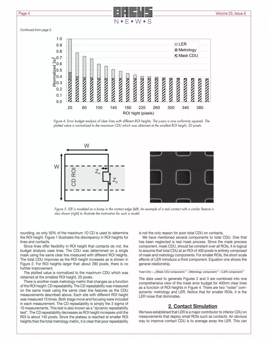
The data used to generate Figures 2 and 3 are combined into one comprehensive view of the mask error budget for 400nm clear lines as a function of ROI heights in Figure 4. There are two “noise” com-ponents: metrology and LER. Notice that for smaller ROIs, it is the LER noise that dominates.
2. Contact SimulationWe have established that LER is a major contributor to inferior CDU on measurements that deploy small ROIs such as contacts. An obvious way to improve contact CDU is to average away the LER. This can
Figure 4. Error budget analysis of clear lines with different ROI heights. The y-axis is now uniformity squared. The plotted value is normalized to the maximum CDU which was obtained at the smallest ROI height, 20 pixels.
Figure 5. LER is modeled as a bump in the contact edge (left). An example of a real contact with a similar feature is also shown (right) to illustrate the motivation for such a model.

Volume 23, Issue 6 Page 5
N • E • W • S
Continues on page 6.
be done by taking an area measurement, or by averaging over several contacts. A good mask metric reliably characterizes the mask features and is indicative of how the same features will print on wafer. A poor metric could yield a number of wafer contact sizes for the same mask contact measurement—a non-unique solution. Wafer simulations are used to compare mask metrics; some of the results are included.
Simulations were conducted with a combination of PROLITH9 and Matlab.10 PROLITH was used to simulate optical printing and resist development for a single contact. Matlab was used to automate the process of simulating many contacts by generating mask layouts, calling PROLITH through the PROLITH Programming Interface (PPI), and postprocessing results to compute the dimensions on mask and on wafer. The PROLITH simulations used a SoftQuad source for wafer illumination conditions,11 attenuated phase shift masks, and a lumped-parameter model for the resist. On the wafer, width measurements were defined as the maximum distance between points in the profile
in resist calculated by PROLITH. Since the contacts on wafer print as circles, this is simply the diameter.
On the mask, two metrics for characterization were used. The first is called the width metric. It was calculated by averaging the width of the contact over a central region of the contact covering 50% of the contact’s height, taking into account a defect if present. This mim-ics the normal CDSEM method. The second metric is one that will effectively increase the ROI, and reduce the LER influence: the area metric. Mask contact area was computed using exact formulas for the geometric shapes used to construct the contact. The impact of each was assessed on the simulated wafer output. To do this, slightly different contact geometries were used for each metric. For example, when exploring corner rounding, simulations for both metrics started with the same nominal geometry: square contacts on the mask. For
Figure 6. Simulated wafer diameter is plotted relative to the Width on Mask (left plots) and vs. Area on Mask (right plots). The top row shows the effect of introducing a bump in one mask contact sidewall. The bottom row shows the effect of rounding the mask contact corners. The simulation data was the same, only the method of characterizing the mask was varied.
Table 1. The uncertainty or range of simulated CD on wafer that is introduced by mask

Page 6 Volume 23, Issue 6
N • E • W • SContinued from page 5.
simulations analyzing the width metric, increased rounding in the cor-ners drove a decrease in the total area of the contact so that the width of the contact was held constant. For simulations analyzing the area metric, the area was held constant so that increased corner rounding forced the width of the contact to increase slightly.
Two mask process variations were introduced to the simulations. Simulations for both metrics covered the same range of process ef-fects, despite the minor differences described above. LER was simu-lated by introducing a bump as is shown in Figure 5. The maximum bump introduced was 2.5nm by 20nm at 1X. The maximum amount of corner rounding was 20nm at 1X. A range of smaller values was also used.
Clearly bumps on the edge of the contact can either fall within the ROI, or outside. Simulations were done both ways and the uncertainty induced on the wafer was calculated from the full range of wafer CDs. The area metric always includes the bumps. The wafer data from simu-lations is plotted two ways: Wafer CD vs. Width on Mask and Wafer CD vs. Area on Mask. The resultant spread on the y-axis is indicative of the range of uncertainties introduced by mask feature variations. The example in Figure 6 shows the examples for mask feature changes induced by a varying corner rounding. Since the family of curves are more tightly clustered when plotted as a function of Mask Area, that is a better predictor of wafer CD than Mask Width.
The full numerical results are summarized in Table 1. In both the bump and corner rounding simulations, the smaller uncertainty values indicate that wafer behavior is predicted better using the mask area metric rather than the mask width metric.
3. Mask contact metrology optionsError budget analysis showed that total contact CDU is increased by the LER component which is minimized by increasing the measurement gate or ROI. For a contact feature, ROI is effectively increased several ways. Multiple measurements could be measured, so that the reported value at a single location is the resultant average. This would minimize LER effects, but it would also increase measurement time. Moreover, potentially important corner rounding information would be neglected. A second alternative is to use an area measurement. Since this area-based uniformity will include contributions from the full length of all four sides (instead of only 50% of two sides), the LER contribution is reduced substantially. The area metric on the CD SEM is calculated as is shown in Figure 7. The contact is divided into 72 wedge-shaped
pieces by generating 5 degree wedges as shown. The area is the sum of all 72 wedge areas (Equation 2). Some error is introduced by the circular edge of each arc, but it is minimal. This will become more evident when we report the area results on real masks.
If the Area Metric were applied to calculate uniformity on production masks, a new specification should be required. The dimension is nm2 and the specification value would depend on contact size itself. An op-tion for control would be to report a percentage variation tolerance, but that is a significant departure from current practices. There is another option. Taking the square root of the Area creates a metric with the same dimension as CD. Hence the uniformity based on this square root of area, or square root area uniformity (SRAU) could be adopted with the conventional CDU specification targets. This has been proposed before and was called the “effective mask contact CD”.1
For illustration, we measured a 400nm clear contact across a mask at 121 locations to obtain a nominal 3 sigma value, x. The same mask was remeasured, but each of the 121 sites was a 5-contact average. This multiple point measurement yielded a 3 sigma that was reduced to 0.79x of the original. This number clearly smoothed the LER compo-nent, but at the cost of considerably more measurement time. Finally, we used the area calculation. This SRAU was based on the data from the single-point measurements so that there was no additional time in the metrology tool. The SRAU was slightly lower, 0.75x, within the tool repeatability of the multiple point average.
A second, more comprehensive, test of using SRAU involved clear lines and contacts on the same mask. Contact SRAU and line CDU were compared using the error budget analysis introduced in Section 1. A 400nm clear line was measured with ROI ranging from 20-400 pixels. 400nm clear contacts were measured two ways: CDU and SRAU. As mentioned in Section 1, contact CDU is similar to line CDU when the same ROI height is deployed. This is illustrated again in Figure 8 at the 53 pixel ROI height. However, it is the SRAU contact uniformity that matches the pure mask CDU for lines at 400 pixel ROI height. This value is significantly better than what would have been obtained with conventional CDU calculations.
We also measured 7 production contact masks to evaluate the use of SRAU in manufacturing. The CDU and SRAU values were tabulated from the same set of measurements and are shown in Figure 9. Since
Figure 7. A schematic representation the area calculation on the CDSEM metrology system.
Figure 8. A bar chart of line CD uniformity is shown along with two contact uniformity measurements on the same mask. SRAU results are close to the line result at realistic ROI heights. The plotted value is normalized to the maximum CDU which was obtained at the smallest ROI height, 20 pixels.
(2)

Volume 23, Issue 6 Page 7
N • E • W • S
CD is measured in both X and Y, the CDSEM scanning direction is orthogonal to the pattern edge. Explicitly, the X-scan is used for verti-cal lines and the Y-scan is used for horizontal lines. Since there are two sets of images available, the SRAU was tabulated using both the X-scan images, SRAU(X), and the Y-scan images, SRAU(Y). Ideally, these two uniformities would be the same. However, minor differences in the scanned images create a small difference in area. In general, the SRAU values are 1-2 nm better than the CD uniformity, as anticipated when LER effects have been minimized.
ConclusionsIt is important to review the key conclusions of earlier sections. First of all, the majority of metrology noise on small contact uniformity measurements comes from LER. This component can be reduced to the level common on lines of the same dimension by reporting the uniformity of the square root area. The reason for taking the square root of the area is that it can be introduced smoothly since the units and target values will be consistent with the former width CD. Simu-lations show that mask area is actually a better predictor of wafer performance than the mask width. While there is definitely a need for the new uniformity methodology for advanced contact masks, there
is still the need to report CD (particularly for asymmetric contacts). There may also be good reason to begin reporting and specifying LER. Since the line edge quality is a separate quantity, it should be treated as such and not lumped together with uniformity.
References1. Mack, C., Microlithography World, Summer 2000. p. 26.2. Sturtevant, J., Opitz, J., and Word, J., Proceedings of the SPIE,
Volume 5040, p. 1055 (2000).3. Kris, R., et al., Proceedings of SPIE, Volume 5256, p. 619 (2003).4. Kris, R., et al, Proceedings of SPIE, Volume 5446, p. 698 (2004).5. Kostler, W., et al., Proceedings of SPIE, Volume 5754, p. 790 (2005).6. Mack, C., Microlithography World, p. 16, Summer 1999.7. Mack, C., Yield Management Solution, p. 76, Spring 2001.8. Mack, C., Sauer, C., Weaver, S., Chabala, J., Proceedings of SPIE,
Volume 4066, p. 172 (2000).9. PROLITH is a registered trademark of KLA-Tencor.10. Matlab is registered trademark of The MathWorks.11. Crouse, M., et al., Proceedings of SPIE, Volume 6154, p. 595 (2006).
Figure 9. CD Uniformity (CDU) and Square Root Area Uniformity (SRAU) are compared on production masks. The uniformity value is normalized to 1.0 at the largest uniformity value in the group, that of Mask B using CD(X).
SPIE is an international society advancing an interdiciplinary approach to the science and application of light.
International HeadquartersP.O. Box 10, Bellingham, WA 98227-0010 USA • Tel: +1 888 504 8171 or +1 360 676 3290 • Fax: +1 360 647 [email protected] • SPIE.org
Shipping Address1000 20th St., Bellingham, WA 98225-6705 USA
2 Alexandra Gate, Ffordd Pengam, Cardiff, CF24 2SA, UK • Tel: +44 29 20 89 4747 • Fax: +44 29 20 89 [email protected] • SPIEeurope.org

Page 8 Volume 23, Issue 6
N • E • W • S
Industry Briefs
Sponsorship OpportunitiesSign up now for the best Photomask 2007 sponsorship opportunities. Contact:
Sue Siegfried Tel: +1 510 728 2105 [email protected]
N • E • W • S
To receive an e-mail announcements of these meetings, send an e-mail message to [email protected]; in the body of the message include the words subscribe info-bacus.
Advertise in the BACUS News!
The BACUS Newsletter is the premier publication serving the photomask industry. For information on how to advertise, contact:
Sue Siegfried Tel: +1 510 728 2105 [email protected]
BACUS Technical Meetings
BACUS holds technical meetings in the Bay Area approximately every quarter, from 8:30 to 11:30 am. If you are interested in presenting a paper at this meeting, contact Robert (Bob) Naber, Cadence Design Systems, Inc., Tel: 510 814 0972; Email: [email protected]
■ What to expect at 45-nmElectronic News/Electronic Business’ Ed Sperling discussed challenges at 45 nm. From an IP perspective, one’s facing process variations at atomic scale. If the assumed gate oxide of four atoms actually is six atoms thick, one’s off by 50 percent. This variation needs to be modeled. With the rollout of 45-nm there has to be a robust ecosystem early in the process development. With model-based DFM, all the information is put it into a data kit, and moved up front to the tool vendors. There would be no working silicon if one doesn’t have DFM factored into design. At the same time, process development is so complex and expensive that most semiconductor vendors are finding they have to partner with a foundry. When fabs are depreciating by millions of dollars a day, getting the ecosystem in place early is important. The vertical disintegration of the IDMs (integrated device manufacturers) is noticeable. The fabless model is here to stay, providing innovation to the end customer. To make an ecosystem successful, a foundry has to develop the process, the design house has to do the IP, and the IDMs have to work closely with the end customer and the EDA to make all of this work. It’s not just foundry’s process and fabless’ IP and tools from an EDA company, without close collaboration. The ecosystem is broader than that: it means collaborating with stepper manufacturers to take their scanner parameters, model them, and put them in with design tools so that design can predict lithography. At the same time, to move from foundry to foundry is more complex and the costs are higher. The EDA flow has to start in the fab, first a virtual one with TCAD tools, so one can model the process and optimize the real fab. That information then has to be brought up into the tools even before the process starts. The choices made during product development are going to impact many customers.
■ Applications aspects to rule chip design
By Christoph Hammerschmidt, EE Times Europe
Mike Fister, CEO of Cadence Applications predicted applications expertise to become the differentiating factor in chip design. Against the background of consumer electronics presently taking the lead in chips consumption over IT-related devices, the global chip market is heading for significant changes. Chips demand for computing applications would flatten out while consumer chips will continue their upward trend, with the highest growth in the RF segment. Major challenges for the EDA industry presently are increasingly congested PCBs, SiPs, embedded software, high speed digital data transport and custom packages. The most challenging part of the design process is verification, especially if applied to complex low power design strategies. At the same time, in an industry where time-to-market dictates ever shorter and faster design cycles, automotive applications take an antithetic position with its extreme long design cycles. The challenge in this segment, however, is not smaller than in the consumer market: “It is the complexity”, Fister said. “Automotive systems actually are systems of systems.” Block level IP and microprocessor cores such as ARM or MIPS are no longer differentiating. Since chip customers demand complete solutions, simple semiconductor expertise will eventually no longer suffice; chip houses will become system houses. What does this mean to mask manufacturing? Mask shops would likely experience increasing complexity in mask databases but less pressure on high end technologies. Whether it would potentially impact the introduction of 32 and 22 nm lithography nodes, remains to be seen, but it appears to be a possibility.
BACUS Corporate Members
Inko Industrials Corporation

Volume 23, Issue 6 Page 9
N • E • W • S
2008SPIE Advanced Lithography
24-29 FebruarySan Jose McEnry Convention CenterSan Jose, California USASPIE.org/al
Photomask Japan
16-18 April Hotel Pacifico YokohamaYokohamna, JapanSPIE.org/jpm
About the BACUS GroupFounded in 1980 by a group of chrome blank users wanting a single voice to interact with suppliers, BACUS has grown to become the largest and most widely known forum for the exchange of technical information of interest to photomask and reticle makers. BACUS joined SPIE in January of 1991 to expand the exchange of information with mask makers around the world.The group sponsors an informative monthly meeting and newsletter, BACUS News. The BACUS annual Photomask Technology Symposium covers photomask technology, photomask processes, lithography, materials and resists, phase shift masks, inspection and repair, metrology, and quality and manufacturing management.
Join the premier professional organization for mask makers and mask users!
Corporate Membership Benefits include:■ One Voting Member in the SPIE General Membership
■ Subscription to BACUS News (monthly)
■ One online SPIE Journal Subscription
■ Exhibit Space discount of 8% at either the Photomask or Advanced Lithography Symposium
■ Listed as a Corporate Member in the BACUS Monthly Newsletter
SPIE.org/bacus-corporate.xml
Individual Membership Benefits include:■ Subscription to BACUS News (monthly)
■ Subscription to Microlithography World (quarterly)
■ Quarterly technical meetings in the Bay Area
■ Reduced registration rates at BACUS Photomask Technology annual meeting
■ Eligibility to hold office on BACUS Steering Committee
SPIE.org/bacus-individual.xml
C a l e n d a r
The 24th European European Mask and Lithography Conference (EMLC 2008)
21-24 January Hilton HotelDresden, Germany www.vde.com/Conferences_en/EMLC+2008/
SPIE/BACUS Photomask Technology
17-21 SeptemberMonterey Marriott & Monterey Conference Ctr.Monterey, California USASPIE.org/pm
You are invited to submit events of interest for this calendar. Please send to [email protected]; alternatively, email or fax to SPIE.
2007
❈
❈
❈
❈

Page 10 Volume 23, Issue 6
N • E • W • SLe
ft im
age:
Co
urte
sy o
f In
tern
atio
nal B
usin
ess
Mac
hine
s C
orp
ora
tion.
Cen
ter
imag
e: C
our
tesy
of
AM
TC
.
Innovation at Work
Sponsored by
Photomask is where equipment suppliers,
lithographers, material manufacturers, researchers,
and mask fabricators share their research, network,
and exchange the latest information. Attend
Photomask and join this integrated effort to look at
factors relevant to design-to-wafer realization.
Network with those in key areas impacting reticle
technology.
Register early and save!
17–21 September 2007Monterey Marriott and Monterey Conference Center
Monterey, California, USA
SPIE.org/photomask