recent progress in gesi electro-absorption modulators
TRANSCRIPT

This content has been downloaded from IOPscience. Please scroll down to see the full text.
Download details:
IP Address: 131.175.59.76
This content was downloaded on 04/12/2013 at 15:28
Please note that terms and conditions apply.
Recent progress in GeSi electro-absorption modulators
View the table of contents for this issue, or go to the journal homepage for more
2014 Sci. Technol. Adv. Mater. 15 014601
(http://iopscience.iop.org/1468-6996/15/1/014601)
Home Search Collections Journals About Contact us My IOPscience
National Institute for Materials Science Science and Technology of Advanced Materials
Sci. Technol. Adv. Mater. 15 (2014) 014601 (8pp) doi:10.1088/1468-6996/15/1/014601
Review
Recent progress in GeSi electro-absorptionmodulatorsPapichaya Chaisakul1, Delphine Marris-Morini1, Mohamed-Said Rouifed1,Jacopo Frigerio2, Daniel Chrastina2, Jean-René Coudevylle1, XavierLe Roux1, Samson Edmond1, Giovanni Isella2 and Laurent Vivien1
1 Institut d’Electronique Fondamentale, Université Paris-Sud, CNRS UMR 8622, Bât. 220, F-91405Orsay Cedex, France2 L-NESS, Dipartimento di Fisica del Politecnico di Milano, Polo di Como, Via Anzani 42, I-22100Como, Italy
E-mail: [email protected] and [email protected]
Received 27 August 2013Accepted for publication 28 October 2013Published 3 December 2013
AbstractElectro-absorption from GeSi heterostructures is receiving growing attention as a highperformance optical modulator for short distance optical interconnects. Ge incorporation withSi allows strong modulation mechanism using the Franz–Keldysh effect and thequantum-confined Stark effect from bulk and quantum well structures at telecommunicationwavelengths. In this review, we discuss the current state of knowledge and the on-goingchallenges concerning the development of high performance GeSi electro-absorptionmodulators. We also provide feasible future prospects concerning this research topic.
Keywords: Electro-absorption, Franz–Keldysh effect, quantum-confined Stark effect, GeSi,multiple quantum wells, optical modulator
1. Introduction
Optics are considered to be one of the most viable solutionsto the performance limitations of electrical interconnection.Optics have now replaced electronic wires for long-haultelecommunication systems [1]. They offer several advantagesover electronics in data transmission, including much higherbandwidth and lower energy dissipation [2, 3]. Moreover,optics are being increasingly deployed in intermediatedistance telecommunication networks, like metropolitan areanetworks and local-area networks [4]. It has become clear thatour unlimited demands for information appear to necessitatethe use of optical data transmission in place of electricalwires at an ever shortening communication distance. The
Content from this work may be used under the terms of theCreative Commons Attribution-NonCommercial-ShareAlike
3.0 licence. Any further distribution of this work must maintain attribution tothe author(s) and the title of the work, journal citation and DOI.
bandwidth and energy dissipation restrictions of copperwire make optical networking preferable, from data centerto the end users and, probably, to the microprocessor.Nevertheless, this poses a serious challenge to the presentoptical technologies based on III–V semiconductors orelectro-optic materials like LiNbO3. These technologies areunlikely to be adopted economically and reliably for such highvolume markets due to small wafer scale and nonstandardizedfabrication. Bringing an optical solution to the largescale integration of silicon (Si) and silicon complementarymetal–oxide–semiconductor (CMOS) electronics is arguablyone of the most promising approaches in allowing highbandwidth optical technology in the mass market. Tosurmount such challenges, Si-compatible optical componentshave been heavily developed and studied in academic andindustrial laboratories during the past decade in order toobtain effective optical propagation, generation, detection andmodulation in/on Si.
1468-6996/14/014601+08$33.00 1 © 2014 National Institute for Materials Science

Sci. Technol. Adv. Mater. 15 (2014) 014601 P Chaisakul et al
1.1. Optical modulation
Optical modulation is indispensable in any opticalinterconnection system. It converts electrical data intothe optical domain and can be obtained either by directlymodulating a light source or by using an optical modulator.An optical modulator allows much higher data rates andmultilevel modulation formats [5]. It can also allow thesystem to be relatively less expensive and have bettertemperature stability [6] because a sophisticated light sourceis not needed and a single light source could be used fordifferent channels with separate optical modulators [7]. Foron-chip application, an off-chip light source with an on-chipoptical modulator could potentially be preferable due toon-chip heat dissipation and temperature variation issues [8].
1.2. Electro-refraction
Electro-refraction is a well-known approach to obtainoptical modulation in Si, as proposed and studied bySoref [9] in 1987. Since the first gigahertz (GHz)Mach–Zehnder interferometer (MZI) modulator was reportedin silicon by Intel in 2004 [10], silicon MZI modulatorshave been intensively studied worldwide [5, 11]. Theyplay a major role in commercially available siliconphotonics-based 100 gigabit optical transceivers, which areaimed for data communication among servers in data centers(www.luxtera.com, www.kotura.com,). However, it appearsthat Si MZI modulators are not likely to meet the futurerequirements of off- and on-chip optical interconnects due tothe relatively weak free carrier dispersion in Si. Because of thelarge size and/or high driving voltage, their energy dissipationof around 1–5 pJ bit−1 is two order of magnitudes higherthan the 2–50 fJ bit−1 expected for timely and progressivereplacement of the electrical interconnection by the opticalinterconnection for off- or on-chip interconnection [8]. Tocircumvent the weak free carrier effect of Si, resonancestructures or slow light enhancements have been proposed.Demonstrations of compact and relatively low-energy opticalmodulators based on these two techniques have recently beenreported by various research teams. Their recent progressand on-going challenges are discussed by other contributionswithin this special issue.
1.3. Electro-absorption
Electro-absorption is another technique that can beused to modulate light. Compared to electro-refraction,electro-absorption typically allows a more compact andlower driving voltage optical modulator [12, 13]. Thiscomponent employs either the Franz–Keldysh effect(FKE) or the quantum-confined Stark effect (QCSE) inmodulating the band gap energy and, hence, absorptioncoefficients. It typically employs III–V direct band gapsemiconductors, which are widely used in nowadayslong-haul and intermediate distance telecommunicationnetworks. Nevertheless, the electro-absorption effect in Sican hardly be useful because it is an indirect band gapsemiconductor with the global minimum of the conduction
band at the 1 valley far from the zone center [14]. As a result,the indirect absorption dominates all of the optical processes,leading to the poor efficiency of optical devices made ofSi optical transition. Incorporation of Ge with Si has beensuggested as a way to enhance the active optical propertiesof the Si photonic platform. Ge, a group IV semiconductorlike Si, has already been included in today’s CMOS chipsin order to improve Si electrical properties [15, 16]. Atroom temperature the direct and indirect gap energies ofGe are ∼0.8 and ∼0.64 eV, respectively [17, 18]. Hence,the Ge direct gap energy of 0.8 eV corresponds well to theC band telecommunication wavelength regions, makingGe an ideal candidate to be engineered for active photonicdevices. Ge incorporation to obtain optical detection attelecommunication wavelength on Si has been reportedsince 1984 [19]. In contrast, its use to achieve strongelectro-absorption in Si-compatible material systems beganto receive serious attention only recently [20]. In this reviewwe will discuss the current state of knowledge and challengesconcerning the development of high performance Ge-richSiGe electro-absorption modulators. We hope that thisreview can play a part in shaping the current understandingand the possible future prospects concerning this researchtopic. This paper will first summarize the electro-absorptionproperties in GeSi. It will then discuss the demonstrateddevice performance in the second part.
2. Electro-absorption in Ge-rich SiGe materialsystems
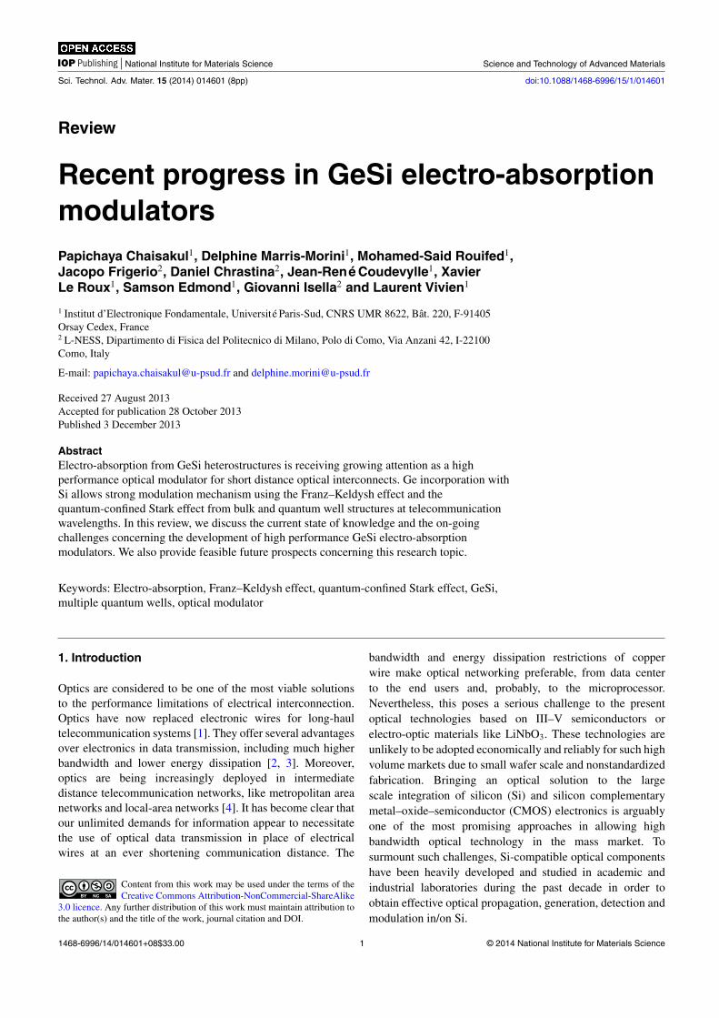
Electro-absorption mechanisms give optical modulationthrough changing the bulk material band gap energy accordingto the applied electric field, which is called the Franz–Keldysheffect (FKE) [21]. An electric field shifts the absorptionedge of the material to the longer wavelengths, enhancingthe absorption coefficients at the weakly absorbing regimeand giving optical modulation as in figure 1(a), which showsthe typical transmission spectra of FKE. The FKE from thedirect band gap absorption of bulk Ge dates back to 1965when it was experimentally demonstrated [22]. Nevertheless,FKE from epitaxial Ge on Si substrate were reported onlyin 2006 [23]. In 2007, Liu et al [24] proposed that aninclusion of a small amount of Si (0.75%) into Ge willenable significant optical modulation from Ge1−x Six at thetelecommunication wavelength of 1.55 µm. It is proposedthat epitaxial Ge0.9925Si0.0075 on Si would have a direct bandgap transition that is slightly higher than 0.8 eV (1.55 µm).The band gap energy was calculated by taking into accountboth the addition of 0.75% Si and the additional tensilestrain of around 0.2% that is induced in Ge0.9925Si0.0075
after high temperature annealing epitaxial steps due to itsthermal expansion coefficient mismatch with Si [25]. Sucha low Si content is expected not to significantly degrade thesharp raise of Ge direct gap absorption when working at1.55 µm [26, 27]. An efficient Ge1−x Six optical modulatorhas been successfully demonstrated by a number of researchteams, as discussed in the following part of this paper.
2

Sci. Technol. Adv. Mater. 15 (2014) 014601 P Chaisakul et al
(a)
(b)
Figure 1. (a) Typical FKE measured from Ge direct gap absorptionband edge. (Reproduced with permission from [51] © 2011 theOptical Society.) (b) QCSE measured from Ge/Si0.15Ge0.85 MQWson Si0.1Ge0.9 relaxed buffer. Two main characteristics of the QCSEare observed: the Stark (red) shift of the absorption spectra and thereduction of the exciton related absorption peak due to the reductionof the overlap between the electron and hole wave functions.
2.1. The quantum-confined Stark effect
QCSE or FKE in quantum well structures, is a strongalternative to realize a high performance opticalmodulator [28]. The interest of using QW structuresresults from its discrete energy levels thanks to the quantumconfinement effect. For optical modulation, this leads toa sharper rise of the absorption edge than in the bulkmaterial; hence, a large variation of absorption coefficientswith a relatively small amount of applied electric fieldsis possible [29]. In Ge, in 2005 Kuo et al [20] fromStanford University reported the breakthrough discoveryof strong QCSE around light wavelength of 1.45 µm atroom temperature from ten periods of 10 nm thick Gewell sandwiched by 16 nm thick Si0.15Ge0.85 barriers(Ge/Si0.15Ge0.85 multiple quantum wells (MQWs)) on aSi0.1Ge0.9 relaxed buffer directly grown on Si substrate. Theabsorption edge is shifted from the 1.55 µm (0.8 eV) of bulkGe due to both the compressive strain induced in Ge QWswith respect to Si0.1Ge0.9 relaxed buffer and the confinement
effect in the QWs. The average Ge concentration in Ge/SiGeMQWs is designed to equal that of the Si0.1Ge0.9 relaxedbuffer in order to achieve epitaxial growth of high qualitythick strain-compensated Ge/SiGe MQWs. The absorptioncoefficients deduced from photocurrent measurementsshow strong QCSE from Ge QWs based on Ge direct-gaptransition between the first valence band heavy hole (HH)level and the first conduction state at 0 (HH1–c01). QCSEfrom Ge QWs is reported to be as strong as that from thedirect-gap III–V semiconductors due to a strong absorptioncoefficient of Ge. This discovery was later studied on a similarGe/Si0.15Ge0.85 MQWs prepared on Si substrate throughthe use of a high growth rate graded buffer by low-energyplasma-enhanced chemical vapor deposition (LEPECVD) atroom and low temperature [30, 31]. Modulation performancewas investigated from both photocurrent and transmissionmeasurements in [31]. Absorption from Ge/SiGe MQWs withan exciton peak having the lowest reported half-width at halfmaximum of 6 meV at room temperature was measured as infigure 1(b). This indicates the good quality of the Ge/SiGeMQWs grown by LEPECVD on a Six Ge1−x graded buffer.
2.2. Polarization dependence of QCSE from Ge/Si0.15Ge0.85
MQWs
Polarization dependence of QCSE from Ge/Si0.15Ge0.85
MQWs has also been explored theoretically andexperimentally [32–36]. Interestingly, using a tight-bindingdescription, Virgilio and Grosso [33] pointed out in 2008 thatthe direct-gap transition between the first valence band lighthole (LH) level and the first conduction state at 0 (LH1–c01)from Ge QWs can have a stronger absorption modulationthan that from the conventionally studied HH1–c01 due toQW optical selection rules and the lower band offset of LHband in Ge/SiGe MQWs [37]. It suggested that LH1–c01absorption and modulation could be significantly enhanced byusing transverse-magnetic (TM) polarized light (electric fieldperpendicular to the QW plan). Only LH related transitionis allowed with combined oscillator strength of HH- andLH-related transitions from the case with transverse-electric(TE) polarized light [38]. In 2009, Virgilio et al [34]experimentally showed a reduction of absorption fromHH1–c01 transition when the polarization changed from TEto TM using prism-shaped structures; nevertheless, due tothe experimental conditions, TM polarized optical absorptionwas not fully enhanced and QCSE was not reported. In 2013,Chaisakul et al [36] performed photocurrent and transmissionspectral measurements on Ge/Si0.15Ge0.85 MQWs to make acomparative study of QCSE from their HH- and LH-relatedtransitions using both TM and TE polarized light. It wasdemonstrated in [36] that the direct-gap transition of Ge QWsexhibited strong polarization dependence, as strong as theone observed from III–V based QWs. The strong QCSE fromLH1–c01 transitions observed from the experiments usingTM polarized light suggested that LH1–c01 transitions couldbe considered in lieu of conventional HH1–c01 transitions toenable a more compact optical modulator by a factor of threewith the same level of modulation efficiency.
3

Sci. Technol. Adv. Mater. 15 (2014) 014601 P Chaisakul et al
2.3. Ge/SiGe MQWs can be engineered to obtain significantQCSE around the telecommunication wavelength of 1.3 µm
Ge/SiGe MQWs can be engineered to obtain significantQCSE around the telecommunication wavelength of 1.3 µm.This can be achieved by either applying a higher level ofcompressive strain on Ge QWs, increasing QW quantumconfinement energy or enlarging the band gap energy ofQWs via Si addition of around 1% [39, 40]. In 2011,Lever et al [41] experimentally reported Ge/Si0.4Ge0.6 ona relaxed Si0.22Ge0.78 buffer. The structures successfullyproduce QCSE around light wavelength of 1.3 µm thanksto larger compressive strain in Ge QWs with respect toSi0.22Ge0.78 relaxed buffer, which is responsible for absorptionedge blue shift. Rouifed et al [42] reported on a similarcomposition of Ge/Si0.35 Ge0.65 on a relaxed Si0.21Ge0.79
buffer in 2012. The modulation performance of Ge/SiGeMQWs when designed to work at shorter wavelengths (e.g.at 1.3 µm) was also worth further discussion. A highercompressive strain increases the energy difference betweenthe bottom of 0- (local minimum of Ge conduction band at thezone center) and L– (global minimum of Ge conduction band)valley conduction band edges. As a result, the absorptionratio between the direct gap transition at 0-valley and thebackground loss of L valley indirect absorption will bereduced. (Absorption at L becomes stronger with respect to0.) This could have an impact on the modulation performancein terms of associated modulation depth and optical loss.
2.4. QCSE from Ge/SiGe MQWs was also investigatedaround the telecommunication wavelength of 1.55 µm
QCSE from Ge/SiGe MQWs was also investigated around thetelecommunication wavelength of 1.55 µm. Kuo et al [43]in 2006 experimentally studied the effect of a decrease incompressive strain and quantum confinement energy in GeQWs, as well as the variation of substrate temperature toachieve QCSE at 1.55 µm with Ge/Si0.175Ge0.825 MQWson a relaxed Si0.05Ge0.95 buffer. The use of Si0.05Ge0.95
relaxed buffer significantly reduced the level of compressivestrain applied on Ge QWs, while a relatively thick GeQWs of 12.5 nm was used to decrease the QW confinementenergy. QCSE was successfully demonstrated around 1.55 µmat a substrate temperature of 90 ◦C, which is comparableto a silicon electronic chip operating environment. It istheoretically predicted that a further reduction of compressivestrain in Ge QWs by using a relaxed Si0.025Ge0.975 buffer [39]or an additional decrease in quantum confinement energyin Ge QWs by using a thicker Ge QWs of 14 nm [40]could allow 1.55 µm QCSE operations at room temperature.It is also worth noticing that care should be taken indecreasing the quantum confinement energy of Ge QWsas it could lead to considerable reduction of excitonicabsorption and, hence, degrading the sharp rise of absorptionedge and modulation performance. In 2011, Ren et al [44]experimentally demonstrated that Ge/Si0.15Ge0.85 MQWs ona Si0.1Ge0.9 relaxed buffer can provide optical modulationfrom light wavelengths of 1450–1550 nm with an appliedelectric field of as high as 20 V µm−1. Additionally,
application of tensile strain can be used to obtain Ge QWswith direct gap transition around 1.55 µm. Chen et al [45]and Carroll et al [46] prepared tensile-strained Ge/SiGeMQWs through tensile-strained Ge virtual substrate, andshowed direct-gap excitonic transition around 1.55 µm fromthe photoluminescence and transmission spectra at roomtemperature. To our knowledge, no QCSE has yet beendemonstrated from such an approach.
It is worth noting that typically in III–V MQWelectro-absorption modulator the absorption saturation dueto the field screening effect could limit the maximum inputpower of the device [47]. Nevertheless, in Ge MQWsthe indirect band-gap of Ge could prevent such an effect.Indeed, the photogenerated carriers suffer for rapid intervalleyscattering from 0 to L, which occurs in hundreds offemtoseconds [48]. In practice one could expect the maximuminput level in Ge MQW electro-absorption modulator to bethe power level that induces nonlinearity, such as two-photonabsorption or four-wave mixing, as in Si electro-refractivemodulators. This nonlinearity power level is normally beyondthat required in one-channel telecommunication systems.
3. GeSi electro-absorption modulator
Significant advances have been made regarding the GeSiFKE optical modulator. Relatively, bulk material is easier togrow and fabricate than QW. To obtain significant opticalmodulation, an FKE modulator is usually based on waveguideconfiguration to allow a long interaction length along thepropagation axis. Liu et al [49] demonstrated the firstGeSi FKE butt-coupled with submicron Si waveguide, as infigure 2(a). It is shown for the first time that an FKE from GeSisystem (0.75% of Si) can provide low energy and fast opticalmodulation with sufficiently large optical bandwidth aroundoptical wavelength of 1.55 µm. In 2012, Feng et al [50]demonstrated an FKE GeSi (0.7% of Si) optical modulatorbutt-coupled with a large cross section Si waveguide platform,as in figure 2(b), which could offer lower fiber couplingloss, waveguide propagation loss, polarization dependent lossand polarization dependent frequency shift compared to thesubmicron waveguide approach. The modulator exhibited acompetitive performance in terms of device footprint, opticalbandwidth, modulation depth, insertion loss, bias voltage andmodulation bandwidth, as summarized in table 1. It is alsopossible to employ bulk Ge for FKE optical modulatorswith optimum modulation efficiency around 1.6 µm [51–53],which should be discussed along with Ge photodetection byanother contribution of this special issue.
3.1. QCSE optical modulators
QCSE optical modulators from Ge/SiGe MQWs havebeen reported in side entry, surface illumination andwaveguide configurations, which are summarized with theaforementioned GeSi FKE modulators in table 1. Theexperimental characterization results from each QCSEmodulator architecture indicate its strong potential to rendercompetitive modulation performance at low voltage due
4

Sci. Technol. Adv. Mater. 15 (2014) 014601 P Chaisakul et al
Table 1. Summary of performance matrices obtained from FKE GeSi and QCSE Ge/SiGe MQW optical modulators experimentallyreported to date.
Dynamicenergy Footprint 3 dB
dissipation of active Voltage Loss at Useful modulation1/4CV2
pp region swing Extinction operating optical bandwidth/(fJ bit−1) (µm2) (VPP) ratio point bandwidth data rate
GeSi FKE 50 1 × 30 3(4–7 V) 8 dB – ∼14 nm 1 GHz[49]
GeSi FKE 60 1 × 55 2.8(0–2.8 V) 6 dB 5 dB ∼30 nm 40 GHz[50]
Ge/SiGe QCSE – 225 × 625 1(3.6–4.6 V) 3 dB – ∼10 nm –[55]
Ge/SiGe QCSE – π × 302 1.5(1–2.5 V)3(0.5–3.5 V) 2.5 dB 3.5 dB <4.5 dB ∼10 nm 3.5 GHz[57]
Ge/SiGe QCSE 0.75 8 1(5.5–6.5 V) 3 dB 15 dB ∼20 nm 7 Gbps[64]
Ge/SiGe QCSE 16 3 × 90 1(3–4 V) 9 dB 12 dB 15 dB 12 dB ∼20 nm 23 GHz[58] 2(2–4 V)5(0–5 V) 11 dB 7.5 dB
(a)
(b)
Figure 2. Schematic representation of: (a) a GeSi FKE modulatorbutt-coupled with submicron Si waveguide in [49] showing for thefirst time that FKE from GeSi system (0.75% of Si) can provide lowenergy and fast optical modulation with significant opticalbandwidth around 1.55 µm; and, (b) a GeSi FKE (0.7% of Si)optical modulator butt-coupled with a large cross section Siwaveguide in [50]. The modulator exhibited a competitiveperformance of device footprint, optical bandwidth, modulationdepth, insertion loss, bias voltage, and modulation bandwidth.(Reproduced with permission from [49] © 2008 Nature PublishingGroup and [50] © 2012 the Optical Society.)
to the strong modulation mechanism of QCSE. In 2007,Roth et al [54] demonstrated Ge/SiGe MQW modulatorwith a side-entry configuration. Using a side-entry approachto facilitate in- and out-coupling of light with Ge/SiGeMQW modulator on Si chip can potentially relax thealignment constraints with the optical fiber compared tothe waveguide architecture. The use of an asymmetricFabry–Perot resonator formed between the active regions ofGe/SiGe MQWs resulted in adequate values of modulationdepth and bandwidth with a reasonable voltage swing.A side-entry design with increasing quality factor of theresonator, as in figure 3(a), was later reported in [55]. Themodulator operating at a driving voltage of 1 V peak-to-peakgave 3 dB modulation contrast around light wavelengthof 1.55 µm at 100 ◦C. A vertical-incidence QCSE opticalmodulator is also of interest. For the free space approach,the use of an on-chip normal incident modulator insteadof VCSEL could be attractive due to its higher thermalstability and lower susceptibility to crystalline defect [8].The characterization of vertical-incidence QCSE opticalmodulator was reported in 2010 and high speed performanceof 3–10 GHz modulation bandwidth was measured from thetested device with optical input and output facet on the topand bottom side of the wafer, respectively [56]. In 2012,Edwards et al [57] demonstrated vertical-incidence QCSEmodulators based on a moderate-Q asymmetric Fabry–Perotcavity formed by distributed Bragg reflector surrounding theGe/SiGe MQWs, as in figure 3(b). The structure allowsthe optical signal to be coupled in and out from the topof the device. An open eye diagram at 2 Gbit s−1 with3.5 GHz 3 dB modulation bandwidth was measured from a60 µm diameter tested device, and substantial improvementmay be expected by further decreasing device dimensions.In 2011, Chaisakul et al [35] reported a QCSE modulatorin a planar waveguide structure from 34 µm long planarwaveguide directly coupled with the input fiber. In 2012,
5

Sci. Technol. Adv. Mater. 15 (2014) 014601 P Chaisakul et al
(a)
(b)
(c)
Figure 3. Schematic representation of: (a) a side-entry QCSEmodulator in [55], showing operation at a driving voltage of 1 Vpeak-to-peak gave 3 dB modulation contrast around lightwavelength of 1.55 µm at 100 ◦C; (b) a vertical-incidence QCSEoptical modulator based on a moderate-Q asymmetric Fabry–Perotcavity formed by distributed Bragg reflector surrounding theGe/SiGe MQWs proposed for free space interconnection in [57];and (c) direct fiber-coupled QCSE optical modulator with 23 GHzmodulation bandwidth and 9 dB extinction ratio for a swing voltageof 1 V between 3 and 4 V in [58]. (Reproduced with permissionfrom [55] © 2008 The Institution of Engineering and Technologyand [57, 58] © 2012 the Optical Society.)
the high speed operation of direct fiber-coupled devicewas reported at 23 GHz from a 3 µm wide and 90 µmlong Ge/SiGe MQW waveguide, as in figure 3(c) [58]. Assummarized in table 1, with a swing voltage of 1 V between3 and 4 V, an extinction ratio of as high as 9 dB wasmeasured with an estimated dynamic energy consumption of16 fJ bit−1 around at light wavelength of 1435 nm. With biasvoltage of 5 V (∼7.5 × 10⁴ V cm−1), 11 dB extinction ratiowith 7.5 dB insertion loss can be simultaneously obtainedat a bit longer light wavelength of 1440 nm. This resultdemonstrated that Ge/SiGe MQWs can render the samemodulation depth as that of III–V based device [59] at similardevice length and electrical bias with an additional optical lossdue to Ge indirect-gap absorption as discussed by Schaevitz
Figure 4. Schematic of a butt coupling integration demonstratedin [64, 65] between a submicron Si waveguide and QCSE opticalmodulator. A record device footprint of 8 µm2 was demonstratedwith estimated dynamic energy consumption of 0.75 fJ bit−1.(Reprint permission from [65] © 2012 the Optical Society.)
et al [60] and Kim and Ahn [61] in 2011. To illustrate,at a comparable device footprint and at their optimumoperating wavelength, while Ge MQW modulator rendered11 dB extinction ratio and 7 dB absorption loss with 5 Vbias (∼7.5 × 10⁴ V cm−1) [58], a direct-gap III–V modulatorresulted in 10 dB extinction ratio and 1 dB absorption losswith 4 V bias (∼11 × 104 V cm−1) [59]. As a perspective,Lim et al [62] recently proposed the use of an add-dropring structure to overcome the indirect-gap absorption ofsilicon–germanium.
3.2. Waveguide-integrated QCSE optical modulators
Waveguide-integrated QCSE optical modulators are alsoimportant as they enable on-chip integration with other opticalfunctionalities, such as detection, propagation and emission.Efficient waveguide integration of QCSE optical modulatorsis significant as performance improvement can be expectedusing QCSE modulator. The experimentally obtained 1α/α
(ratio between absorption change and background absorptionloss) of Ge QCSE was shown to be as high as 3.6 at itsoptimum operating wavelength [20], while for bulk GeSi the1α/α was experimentally reported to be approximately 2,although much improvement can be expected according to thetheoretical simulation [50]. In 2012, Ren et al [63] studiedbutt coupling integration between a submicron Si waveguideand Ge/SiGe MQWs. A Ge/SiGe MQW optical modulator,as in figure 4, with record device footprint of 8 µm2 wasdemonstrated with estimated dynamic energy consumption of0.75 fJ bit−1 [64]. The demonstrator exhibited relatively highcoupling loss due to the mode mismatch between the thinSi waveguide core and the thick Ge/SiGe MQWs modulatorregion. Claussen et al [65] later demonstrated that integrationwith a large core Si waveguide platform is possible; therefore,a minimized optical coupling loss could be expected in thefuture. Evanescent coupling is also a promising approach forefficient optical coupling between the Si waveguide and theGe active layers [66]. The taper section required for adiabaticcoupling can be normally long and increases the devicefootprint. Nevertheless, in 2012 Lever et al [67] proposed atwo step taper approach which can significantly reduce taperlength compared to the conventional linear taper approach.Although no practical evanescent coupling QCSE modulatorhas yet been demonstrated, recent optical simulation showsthat an efficient waveguide-integrated QCSE modulator canbe fabricated based on this concept [68].
6

Sci. Technol. Adv. Mater. 15 (2014) 014601 P Chaisakul et al
4. Conclusions
In conclusion, electro-absorption from GeSi on Si is one of themost promising candidates to realize a compact, low-energy,fast, temperature stable and high-volume optical modulatorfor short distance optical interconnects. High performanceoptical modulators have been demonstrated by both FKEand QCSE. For waveguide integration, an FKE modulatorbutt coupled with Si waveguide has been shown withacceptable performance matrix, while efficient integration ofQCSE device with input and output waveguide is still underdevelopment. Significant progress can be expected within thenext few years given the current pace of work. Concerningdevice performance, it should be noted that the requirementsof an optical modulator varies according to applications andthe performance matrix of short scale interconnects can beconsiderably different than those conventionally applied tolong-haul or intermediate distance optical communication.For example, it was mentioned that an optical modulatorwith 5 dB extinction ration with 3 dB insertion loss could beconsidered suitable for chip scale communication [40], whichis significantly lower than 15–20 dB modulation requiredfor long-haul optical networks. On the contrary, energydissipation is more critical for chip scale interconnects dueto the definite limit of power dissipation available on a chip.Although it is not certain which of the competing solutions(resonator, slow light, GeSi) will emerge as the most suitableoption for short distance optical communication, all indicatea potential to produce sufficiently strong optical modulationwith satisfactory values of related performance matrix. Thesuccessful development of an optical modulator that can beintegrated seamlessly with CMOS integrated circuits shouldbe one of the keys in overcoming the delay, power andbandwidth limitations of metal interconnects from the datacenter to the end users, and down to the microprocessor.
References
[1] Kirchain R and Kimerling L 2007 Nature Photon. 1 303[2] Miller D A B 1997 Int. J. Optoelectron. 11 155[3] Miller D A B 2000 Proc. IEEE 88 728[4] Reed G T and Knights A P 2004 Silicon Photonics: An
Introduction (New York: Wiley)[5] Reed G T, Mashanovich G Z, Gardes F Y and Thomson D J
2010 Nature Photon. 4 518[6] Kekatpure R D and Lentine A 2013 Opt. Express 21 5318[7] De Dobbelaere P et al 2012 Si photonics based high-speed
optical transceivers European Conf. and Exhibition onOptical Communication (Washington, DC: Optical Societyof America) paper We.1.E.5
[8] Miller D A B 2009 Proc. IEEE 97 1166[9] Soref R and Bennett B 1987 IEEE J. Quantum Electron 23 123
[10] Liu A, Jones R, Liao L, Samara-Rubio D, Rubin D, Cohen O,Nicolaescu R and Paniccia M 2004 Nature 427 615
[11] Marris-Morini D et al 2009 Proc. IEEE 97 1199[12] Steinmann P, Borchert B and Stegmuller B 1997 IEEE Photon.
Technol. Lett. 9 1561[13] Fukano H, Yamanaka T and Tamura M 2007 J. Light. Technol.
25 1961[14] Cardona M and Pollak F H 1996 Phys. Rev. 142 530[15] Schaffler F 1997 Semicond. Sci. Technol. 12 1515[16] Cressler J D 1998 IEEE Trans. Microw. Theory Tech. 46 572
[17] MacFarlane G G, McLean T P, Quarrington J E and Roberts V1957 Phys. Rev. 108 1377
[18] Dash W C and Newman R 1955 Phys. Rev. 99 1151[19] Luryi S, Kastalsky A and Bean J C 1984 IEEE Trans. Electron.
Dev. ED-31 1135[20] Kuo Y-H, Lee Y K, Ge Y, Ren S, Roth J E, Kamins T I,
Miller D A B and Harris J S 2005 Nature 437 1334[21] Keldysh L V 1957 J. Exp. Theor. Phys. 33 994[22] Frova A and Handler P 1965 Phys. Rev. 137 A1857[23] Jongthammanurak S, Liu J, Wada K, Cannon D D,
Danielson D T, Pan D, Kimerling L C and Michel J 2006Appl. Phys. Lett. 89 161115
[24] Liu J, Pan D, Jongthammanurak S, Wada K, Kimerling L Cand Michel J 2007 Opt. Express 15 623
[25] Ishikawa Y, Wada K, Cannon D D, Liu J, Luan H-C andKimerling L C 2003 Appl. Phys. Lett. 82 2044
[26] Luo Y et al 2011 Proc. SPIE 7944 79440P[27] Braunstein R, Moore A R and Herman F 1958 Phys. Rev.
109 695[28] Miller D A B, Chemla D S, Damen T C, Gossard A C,
Wiegmann W, Wood T H and Burrus C A 1984 Phys. Rev.Lett. 53 2173
[29] Miller D A B, Chemla D S, Damen T C, Gossard A C,Wiegmann W, Wood T H and Burrus C A 1985 Phys. Rev. B32 1043
[30] Tsujino S, Sigg H, Mussler G, Chrastina D and Von Känel H2006 Appl. Phys. Lett. 89 262119
[31] Chaisakul P, Marris-Morini D, Isella G, Chrastina D,Le Roux X, Gatti E, Edmond S, Osmond J, Cassan E andVivien L 2010 Opt. Lett. 35 2913
[32] Paul D J 2008 Phys. Rev. B 77 155323[33] Virgilio M and Grosso G 2008 Phys. Rev. B 77 165315[34] Virgilio M, Bonfanti M, Chrastina D, Neels A, Isella G,
Grilli E, Guzzi M, Grosso G, Sigg H and von Känel H 2009Phys. Rev. B 79 075323
[35] Chaisakul P, Marris-Morini D, Isella G, Chrastina D,Le Roux X, Edmond S, Cassan E and Vivien L 2011 Opt.Lett. 36 1794
[36] Chaisakul P et al 2013 Appl. Phys. Lett. 102 191107[37] Schaevitz R K, Roth J E, Ren S, Fidaner O and Miller D A B
2008 IEEE J. Sel. Top. Quantum Electron. 14 1082[38] Bastard G 1988 Wave Mechanics Applied to Semiconductor
Heterostructures (Les Ulis: Les Editions de Physique)[39] Lever L, Ikonic Z, Valavanis A, Cooper J and Kelsall R 2010
J. Light. Technol. 28 3273[40] Schaevitz R K, Edwards E H, Roth J E, Fei E T, Rong Y,
Wahl P, Kamins T I, Harris J S and Miller D A B 2012 IEEEJ. Quantum Electron. 48 187
[41] Lever L et al 2011 Opt. Lett. 36 4158[42] Rouifed M S, Chaisakul P, Marris-Morini D, Frigerio J,
Isella G, Chrastina D, Edmond S, Le Roux X,Coudevylle J-R and Vivien L 2012 Opt. Lett. 37 3960
[43] Kuo Y-H, Lee Y K, Ge Y, Ren S, Roth J E, Kamins T I,Miller D A B and Harris J S 2006 IEEE J. Sel. Top.Quantum Electron. 12 1503
[44] Ren S, Rong Y, Kamins T I, Harris J S and Miller D A B 2011Appl. Phys. Lett. 98 151108
[45] Chen Y, Li C, Lai H and Chen S 2010 Nanotechnology21 115207
[46] Carroll L, Imbert F, Sigg H, Süess M, Müller E, Virgilio M,Pizzi G, Rossbach P, Chrastina D and Isella G 2011 Appl.Phys. Lett. 99 031907
[47] Weiner J S, Chemla D S, Miller D A B, Haus H A, GossardA C, Wiegmann W and Burrus C A 1985 Appl. Phys. Lett.47 664
[48] Claussen S A, Tasyurek E, Roth J E and Miller D A B 2010Opt. Express 18 25596
[49] Liu J, Beals M, Pomerene A, Bernardis S, Sun R, Cheng J,Kimerling L C and Michel J 2008 Nature Photon. 2 433
7

Sci. Technol. Adv. Mater. 15 (2014) 014601 P Chaisakul et al
[50] Feng D et al 2012 Opt. Express 20 22224[51] Feng N-N et al 2011 Opt. Express 19 7062[52] Lim A E-J, Liow T-Y, Qing F, Duan N, Ding L, Yu M, Lo G-Q
and Kwong D-L 2011 Opt. Express 19 5040[53] Schmid M, Kaschel M, Gollhofer M, Oehme M, Werner J,
Kasper E and Schulze J 2012 Thin Solid Films 525 110[54] Roth J E, Fidaner O, Schaevitz R K, Kuo Y-H, Kamins T I,
Harris J S and Miller D A B 2007 Opt. Express 155851
[55] Roth J E, Fidaner O, Englund E E, Schaevitz R K, Kuo Y-H,Helman N C, Kamins T I, Harris J S and Miller D A B 2008Electron. Lett. 44 49
[56] Rong Y, Ge Y, Huo Y, Fiorentino M, Tan M R T, Kamins T I,Ochalski T J, Huyet G and Harris J S 2010 IEEE J. Sel. Top.Quantum Electron. 16 85
[57] Edwards E H, Audet R M, Fei E T, Claussen S A, SchaevitzR K, Tasyurek E, Rong Y, Kamins T I, Harris J S andMiller D A B 2012 Opt. Express 20 29164
[58] Chaisakul P, Marris-Morini D, Rouifed M-S, Isella G,Chrastina D, Frigerio J, Le Roux X, Edmond S,Coudevylle J-R and Vivien L 2012 Opt. Express 20 3219
[59] Kuo Y-H, Chen H-W and Bowers J E 2008 Opt. Express16 9936
[60] Schaevitz R K, Ly-Gagnon D S, Roth J E, Edwards E H andMiller D A B 2011 AIP Adv. 1 032164
[61] Kim J and Ahn D 2011 J. Appl. Phys. 110 083119[62] Lim P H, Cai J, Ishikawa Y and Wada K 2012 Opt. Lett.
37 1496[63] Ren S, Kamins T I and Miller D A B 2011 IEEE Photon.
J. 3 739[64] Ren S, Rong Y, Claussen S A, Schaevitz R K, Kamins T I,
Harris J S and Miller D A B 2012 IEEE Photon. Technol.Lett. 24 461
[65] Claussen S A, Balram K C, Fei E T, Kamins T I, Harris J S andMiller D A B 2012 Opt. Mater. Express 2 1336
[66] Ahn D, Kimerling L C and Michel J 2011 J. Appl. Phys.110 083115
[67] Lever L, Ikonic Z and Kelsall R W 2012 Opt. Express20 29500
[68] Edwards E H, Lever L, Fei E T, Kamins T I, Ikonic Z, HarrisJ S, Kelsall R W and Miller D A B 2013 Opt. Express21 867
8