question bank for multiple choice questions 1. conductivity
TRANSCRIPT
Page 1 of 103
Question Bank for Multiple Choice Questions
1. Conductivity of Materials
Marks:-18
Content of Chapter:-
1.1.Termsand factors affecting the resistivity of electrical materials
1.2 Electron mobility, energy level diagram of a material
1.3 Emission of electrons from metals-Thermonic emission, photo electronic emission ,field emission,
secondary emission concept, material and application
1.4 Effect of temperature on conductivity of metals, superconductivity, electrical and thermal conductivity of
metals. Thermoelectric effect: concept, materials and applications
1 Thermal conductivity is defined as the heat flow per unit time
a) When the temperature gradient is unity
b) Across the wall with no temperature
c) Through a unit thickness of the wall
d) Across unit area where the temperature gradient is unity
Answer: d
Explanation: Thermal conductivity of a material is because of migration of free electrons and lattice
vibrational waves.
2 Mark the matter with least value of thermal conductivity
a) Air
b) Water
c) Ash
d) Window glass
Answer: a
Explanation: For air, it is .024 W/ m degree i.e. lowest.
3 Which one of the following forms of water has the highest value of thermal conductivity?
a) Boiling water
b) Steam
c) Solid ice
d) Melting ice
View Answer
Answer: c
Explanation: For ice, it is 2.25 W/m degree i.e. maximum.
ZEAL EDUCATION SOCIETY’S
ZEAL POLYTECHNIC,PUNE
NARHE │PUNE -41 │ INDIA
DEPARTMENT OF E&Tc ENGINEERING
Program: Diploma in E&Tc engineering Program Code:- EJ
Scheme:-I Semester:-2
Course:- Electronic Engineering Materials Course Code:- 22217
Page 2 of 103
4 The average thermal conductivities of water and air conform to the ratio
a) 50:1
b) 25:1
c) 5:1
d) 15:1
Answer: b
Explanation: For water, it is 0.55-0.7 W/m degree and for air it is .024 W/m degree.
5 Identify the very good insulator
a) Saw dust
b) Cork
c) Asbestos sheet
d) Glass wool
Answer: d
Explanation: Glass wool has a lowest thermal conductivity of 0.03 W/m degree amongst given
option.
6 Most metals are good conductor of heat because of
a) Transport of energy
b) Free electrons and frequent collision of atoms
c) Lattice defects
d) Capacity to absorb energy
Answer: b
Explanation: For good conductors, there must be electrons that are free to move.
7 Heat conduction in gases is due to
a) Elastic impact of molecules
b) Movement of electrons
c) EM Waves
d) Mixing of gases
Answer: a
Explanation: If there is elastic collision then after sometime molecules regain its natural position.
8 The heat energy propagation due to conduction heat transfer will be minimum for
a) Lead
b) Water
c) Air
d) Copper
Answer: c
Explanation: It is because air has lowest value of thermal conductivity amongst given options.
Page 3 of 103
9 Cork is a good insulator because
a) It is flexible
b) It can be powdered
c) Low density
d) It is porous
Answer: d
Explanation: Cork has thermal conductivity in the range of 0.05-0.10 which is very low so it can be
porous.
10 Choose the false statement
a) For pure metal thermal conductivity is more
b) Thermal conductivity decreases with increase in the density of the substance
c) Thermal conductivity of dry material is lower than that of damp material
d) Heat treatment causes variation in thermal conductivity
Answer: b
Explanation: Thermal conductivity increase with increase in the density of a substance.
11
When one end of the rod is heated, the molecules at the hot end vibrate with higher amplitude and
transmit the heat from one particle to the adjacent particle and so on. What is the process?
a) Convection
b) Conduction
c) Radiation
d) Transmittance
Answer: b
Explanation: In the above condition, heat is transmitted by the vibration of particles. Conduction is
the process in which heat is transferred from hotter end to colder end without the actual motion of
particles. Therefore, it is conduction.
12 Solids with weekly bonded electrons are good conductors of heat.
a) True
b) False
Answer: a
Explanation: Transmission of heat depends upon the outermost electrons. Therefore solids with
weekly bonded electrons are good conductors of heat.

Page 4 of 103
13
When potassium is added to water, it is seen that the lower region becomes warm first and
becomes less dense. It then moves up and the more dense cold water comes down and the
process goes on. What is the process taking place?
a) Radiation
b) Conduction
c) Convection
d) Purification
Answer: c
Explanation: Convection is the process in which heat is transmitted from hotter end to colder end
by actual movement of heated particles. Since the particles are actually moving in the above
process, it is convention.
14 Why is the roof of buildings painted white?
a) Because it absorbs radiation
b) Because it reflects radiations
c) Because it is cheaper
d) Because it conducts heat
Answer: b
Explanation: Black objects are good absorbers and radiators while white surfaces are poor
absorbers and radiators. Therefore houses are painted white to keep the building cool during
summer.
15 What happens when a material is heated?
a) It contracts
b) It melts
c) It expands
d) It bursts
Answer: c
Explanation: Most materials expand on heating because the particles are moving about a higher
average speed and therefore have a higher energetic collision.
16 Why locations next to large water bodies tend to have a moderate climate than those further inland?
a) Because of the latitude
b) Because of specific heat of water
c) Because of the heating effects of sun
d) Because of the water in clouds
Answer: b
Explanation: It takes a longer time to heat up or cool down a given mass of water than an equal
mass of aluminium or iron. This high specific heat of water makes it easy for cooling and warming.
This is why the locations next to larger water bodies tend to have a moderate climate than those
further inland.
Page 5 of 103
17
The outer ends of two bars A and B are at 100°C and 50° respectively. Calculate the temperature
at the welded joint if they have the same cross-section and the same length and their thermal
conductivities are in the ratio of A:B = 7:5.
a) 79.166°C
b) 80.548°C
c) 20.157°C
d) 58.147°C
Answer: a
Explanation: K1/K2 = (θ2-θ3)/(θ1-θ2)
θ2= 79.166℃
18
What happens when you heat china having some dark paintings engraved on it at 1000°C and then
examine it in a dark room immediatel ?
a) The dark painting will appear much brighter
b) The whole china dish will be bright
c) The china dish doesn’t glow
d) The china dish will develop patterns
Answer: a
Explanation: According to Kirchhoff’s law, if a body strongly absorbs radiation of a certain
wavelength, it must emit strongly the radiation of the same wavelength. The dark paintings are
better absorbers, and therefore, also better emitters.
19 A green glass heated in a furnace when taken out in dark glows red.
a) False
b) True
Answer: b
Explanation: Green glass, when cold, is a good absorber of red light and a good reflector of green
light. When heated, it becomes a good emitter of red light in accordance with Kirchhoff’s law.
20
Two thermometers are constructed in the same way except that one has a spherical bulb and the
other an elongated cylindrical bulb. Which of the two will respond quickly to temperature changes?
a) Spherical bulb
b) Elongated cylindrical bulb
c) All of the mentioned
d) None of the mentioned
Answer: a
Explanation: A cylindrical bulb has a greater surface area than a spherical bulb of the same volume.
Hence the thermometer with elongated cylindrical bulb will respond to temperature changes more
quickly than the one with a spherical bulb.
21 The temperature of a body can be negative on the Kelvin scale.
a) True
b) False
Answer: b
Page 6 of 103
Explanation: The temperature of a body cannot be negative on a Kelvin scale because the absolute
zero on the Kelvin scale is the minimum possible temperature.
22 Which of the following is an effective coolant?
a) Oil
b) Mercury
c) Water
d) Acids
Answer: c
Explanation: The specific heat of water is very high. When it runs over hot parts of the engine or
machinery, it absorbs a large amount of heat. This helps in maintaining the temperature of the
engine low.
23 Conductivity is defined as the ability to carry ____________
a) Voltage
b) Resistance
c) Current
d) All of the mentioned
Answer: c
Explanation: Conductivity is defined as the ability to carry current. It is measured by the flow of
electrons and charges through a conductor.
24 The reciprocal of conductivity is ____________
a) Viscosity
b) Resistivity
c) Turbidity
d) None of the mentioned
Answer: b
Explanation: The reciprocal of conductivity is resistivity. It is the measure of resistance provided in
the path of electrons.
25 Which of the following is a specific conductivity reagent?
a) KCl
b) HCl
c) NaCl
d) MgCl2
Answer: a
Explanation: KCl is a specific conductivity reagent. Specific conductance is a measure of the electric
current in the water sampled carried by the ionized substances.
Page 7 of 103
26 The internationally recommended unit for conductance is ____________
a) Poise
b) Dyne
c) Ohm
d) Siemens
Answer: d
Explanation: The internationally recommended unit for conductance is Siemens (S). 1 siemen = 1
ohm-1
27 The cell constant is defined as the ratio of ____________
a) Area of either electrodes to the length between the electrodes
b) Length between the electrodes to the area of either electrodes
c) Length between the electrodes to the volume of either electrode
d) Resistivity to conductivity
Answer: b
Explanation: The cell constant is defined as the ratio of length between the electrodes to the area of
either electrodes. It only depends upon the physical dimension of the cell.
28 Choose the correct order of molar ionic conductivities of the following ions.
a) Li+ < Na+ < K+ < Rb+
b) Li+ < K+ < Rb+ < Na+
c) Li+ < Na+ < Rb+ < K+
d) Li+ < Rb+ < Na+ < K+
Answer: a
Explanation: the correct order of molar ionic conductivity is- Li+ < Na+ < K+ < Rb+.
29 On which factor does the conductance of electrolytic solutions depend?
a) Temperature and pressure
b) Number of charge carriers
c) Dielectric constant of the solvent
d) All of the mentioned
Answer: d
Explanation: The factors on which conductance of electrolytic solution depends are- Temperature,
pressure, number of charge carriers and dielectric constant of the solvent.
30 On dilution, the specific conductance ____________
a) Increases
b) Remains same
c) Decreases
d) None of the mentioned
Answer: c
Explanation: On dilution, the specific conductance decreases because dilution decreases the
concentration of the solution.
Page 8 of 103
31
The equivalent conductance of 0.1 H2SO4offering a resistance of 50ohms when placed in a
conductivity cell whose electrodes are 1cm apart with a cross-sectional area of 2cm2 at 250C is?
a) 100 S cm2 eq-1
b) 1000 S cm2 eq-1
c) 10 S cm2 eq-1
d) 1 S cm2 eq-1
Answer: a
Explanation: The equivalent molar conductance is 100 S cm2 eq-1.
Conductivity = Conductance * cell constant
Cell constant = Length / Area
32 Dilution means an increase in the amount of ____________
a) Solute
b) Solvent
c) Electrolyte
d) All of the mentioned
Answer: b
Explanation: Dilution means an increase in the amount of solvent and hence it decreases the
concentration of solute particles.
33 Thermocouple is a ______________
a) Primary device
b) Secondary transducer
c) Tertiary transducer
d) None of the mentioned
Answer: a
Explanation: Thermocouple is a device which converts thermal energy to electrical energy and it
can be treated as a primary device.
34 Operation of thermocouple is governed by _______________
a) Peltier effect
b) Seebeck effect
c) Thomson effect
d) All of the mentioned
Answer: d
Explanation: Operation of thermocouple is based on three major effects- Peltier, Thomson and
seebeck, all describe the relation between current flow and temperature between two different
metal.
35 ______________ describes current flow between two junctions formed by two different metals.
a) Peltier effect
b) Thomson effect
c) Seebeck effect
d) None of the mentioned
Answer: a
Page 9 of 103
Explanation: When two different metals are connected to form two junctions, current flow will occur
from one junction to other. This is described by peltier effect.
36 Amount of heat liberated or absorbed when 1A current passes is called ____________
a) Thomson coefficient
b) Peltier coefficient
c) Seebeck coefficient
d) None of the mentioned
Answer: b
Explanation: Peltier coefficient relates heat liberated or absorbed and current flow.
37 Total seebeck effect can be found as _____________
a) Total peltier effect
b) Total Thomson effect
c) Partly peltier and partly Thomson effect
d) None of the mentioned
Answer: c
Explanation: All three effects, peltier, seebeck and Thomson effects are connected to each other,
and total seebeck effect can be found as partly peltier and partly Thomson effect.
38 Which of the following element is used as a thermocouple in nuclear reactor?
a) Boron
b) Platinum
c) Copper
d) Iron
Answer: a
Explanation: Nuclear reactors are places where a large amount of heat is liberated, here boron is
used as thermocouple element as it can measure temperature above 15000c.
39 Thermocouple cannot used for measurement of temperature of liquid.
a) True
b) False
Answer: b
Explanation: Immersion type thermocouple can be used to measure temperature of liquid, in which
thermocouple is immersed in liquid.
40 _________________ can be used as a replacement for thermocouple lead.
a) Replacement lead
b) Replica lead
c) Compensating lead
d) None of the mentioned
Answer: c
Explanation: Compensating leads are of the same materials as thermocouple leads and can be
used as a replacement.
Page 10 of 103
41 Thermo couple cannot be used to measure ____________
a) Temperature of gas
b) Temperature of liquid
c) IR radiation
d) None of the mentioned
Answer: d
Explanation: Infra-Red radiation is characterized by temperature and thermocouple can be used to
measure temperature.
42 Peltier effect is reverse of seebeck effect.
a) True
b) False
Answer: a
Explanation: Peltier effect and seebeck effect operations are reverse to each other.
Prepared By
Badadhe P S
Verified By
Jadhav D G
Module Coordinator
Re-Verified By
Navale S N
Academic Coordinator
Approved By
Tupe S G
HoD E&Tc
Page 11 of 103
ZEAL EDUCATION SOCIETY’S
ZEAL POLYTECHNIC,PUNE
NARHE │PUNE -41 │ INDIA
DEPARTMENT OF E&Tc ENGINEERING
Question Bank for Multiple Choice Questions
02 – Dielectric materials
Marks:-16
2.1 Effect of dielectric on behavior of capacitor, frequency dependence of electronic polarisability
frequency dependence of permittivity, Dielectric properties
2.2 Frequency dependence of electronic polarisability
2.3 Frequency dependence of permittivity.
2.4 Dielectric properties of polymeric material
2.5 Insulating materials Breakdown in gaseous, liquid and solid dielectric materials
2.6 Requirements of good insulating materials
2.7 Dielectric materials-mica, porcelain, polythene, polyvinycarboide (PVC), rubber, cotton and silk,
glass, paper and boards, wood, enamel covering transformer oil, polymers, properties and applications
2.8 Ferroelectricity and piezoelectricity concept, materials and applications.
1 Which of the following is the correct expression for the dielectric strength?
a) d/Vb
b) Vb/d
c) Vbd
d) Vb/d2
Answer: b
Explanation: The dielectric strength is also defined as the maximum potential gradient to which a
dielectric can be subjected with insulation breakdown. The expression is: Vb/d, where Vb is the
breakdown voltage and d is the thickness of the specimen.
2 Mica has a dielectric strength of _____________
a) 50 X 106 V/m
b) 100 X 106 V/m
c) 150 X 106 V/m
d) 200 X 106 V/m
Answer: b
Explanation: Mica has one of the highest dielectric strengths of 100 X 106 V/m. It is widely used for
insulation purposes.
3 Beyond breakdown voltage, dielectrics become insulating.
a) True
b) False
Answer: b
Page 12 of 103
Explanation: Dielectrics are defined as materials devoid of free charges. After the breakdown
voltage, it loses its insulating property and becomes conducting.
4 Dielectric breakdown occurs in gases due to ____________
a) Corona Discharge
b) Dielectric heating
c) Intrinsic breakdown
d) Defect breakdown
Answer: a
Explanation: Dielectric breakdown occurs in gases due to the corona discharge in non-uniform
fields or due to photoionization and collision of electrons with gas atoms.
5 In which type of breakdown, an avalanche of electrons is formed?
a) Defect Breakdown
b) Thermal Breakdown
c) Intrinsic Breakdown
d) Electrochemical Breakdown
Answer: c
Explanation: At high Electric fields, electrons are ejected which are accelerated through the
material, producing an avalanche of electron. Such a breakdown is called intrinsic
breakdown.
6 The presence of porosity in dielectrics is detrimental for higher dielectric strength.
a) True
b) False
Answer: a
Explanation: The more holes of cracks there are in the dielectric solid, the more ionization of
gases would take place in that pores at higher electric field. This leads to thermal stress which
generates cracks. Thus, the presence of porosity is detrimental for higher dielectric strength.
7 The process of breakdown is accelerated by the presence of ____________
a) Impurities
b) Conduction
c) Humidity
d) Magnetic Field
Answer: a
Explanation: The process of breakdown of liquids is accelerated by the presence of impurities
or high concentration of mobile ions (e.g. Na+, Li+) in liquids.
8 The most common mode of breakdown in ceramic insulators is _____________
a) Defect Breakdown
b) Thermal Breakdown
c) Intrinsic Breakdown
d) Electrochemical Breakdown
Answer: b
Page 13 of 103
Explanation: Thermal breakdown occurs due to local heating or conduction losses which
generate heat at the rate faster than it can be dissipated. This is most common in ceramics.
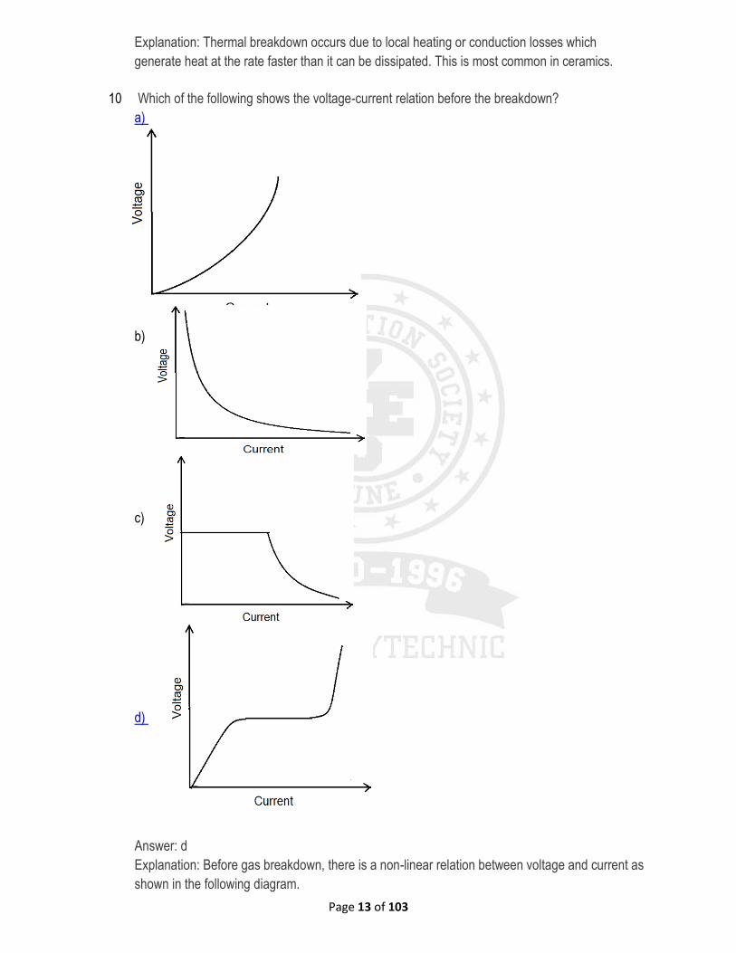
10 Which of the following shows the voltage-current relation before the breakdown?
a)
b)
c)
d)
Answer: d
Explanation: Before gas breakdown, there is a non-linear relation between voltage and current as
shown in the following diagram.
Page 14 of 103
11 A dielectric is always an insulator. But an insulator is not necessarily a dielectric. State True/False.
a) True
b) False
Answer: a
Explanation: For a material to be dielectric, its permittivity should be very high. This is seen in
insulators. For a material to be insulator, the condition is to have large band gap energy. However,
this is not necessary for a dielectric.
12 Identify a good dielectric.
a) Iron
b) Ceramics
c) Plastic
d) Magnesium
Answer: b
Explanation: Iron and magnesium are metals. Hence they need not be considered. Both ceramics
and plastic are insulators. But dielectric constant is more for ceramics always. Hence ceramics is
the best dielectric.
13 A dielectric can be made a conductor by
a) Compression
b) Heating
c) Doping
d) Freezing
Answer: b
Explanation: On increasing the temperature, the free electrons in an insulator can be promoted from
valence to conduction band. Gradually, it can act as a conductor through heating process. This
condition is called dielectric breakdown, wherein the insulator loses its dielectric property and starts
to conduct.
14 Find the dielectric constant for a material with electric susceptibility of 4.
a) 3
b) 5
c) 8
d) 16
Answer: b
Explanation: The electric susceptibi ity is given by χe = εr – 1. For a susceptibility of 4, the dielectric
constant will be 5. It has no unit.
15 For a dielectric which of the following properties hold good?
a) They are superconductors at high temperatures
b) They are superconducto s at low temperatures
c) They can never become a superconductor
d) They have very less dielectric breakdown voltage
Answer: b
Page 15 of 103
Explanation: Superconductors are characterised by diamagnetism behaviour and zero resistivity,
which true for a dielectric. They occur only at low temperature. Thus a dielectric can become a
superconductor at low temperatures with very high dielectric breakdown voltage.
16 The magnetic field which destroys the superconductivity is called
a) Diamagnetic field
b) Ferromagnetic field
c) Ferrimagnetic field
d) Critical field
Answer: d
Explanation: Critical field is that strong magnetic field which can destroy the superconductivity of a
material. The temperature at which this occurs is called transition temperature.
17 The magnetic susceptibility in a superconductor will be
a) Positive
b) Negative
c) Zero
d) Infinity
Answer: b
Explanation: Due to perfect diamagnetism in a superconductor, its magnetic susceptibility will be
negative. This phenomenon is called Meissner effect.
18 The superconducting materials will be independent of which of the following?
a) Magnetic field
b) Electric field
c) Magnetization
d) Temperature
Answer: b
Explanation: Superconducting materials depends only on the applied magnetic field, resultant
magnetization at the temperature considered. It is independent of the applied electric field and the
corresponding polariz
19 Find the mean free path of an electron travelling at a speed of 18m/s in 2 seconds.
a) 9
b) 36
c) 0.11
d) 4.5
Answer: b
Explanation: The mean free path is defined as the average distance travelled by an electron before
collision takes place. It is given by, d = v x ηc, where v is the velocity and ηc is the collision time.
Thus d = 18 x 2 = 36m.
Page 16 of 103
20 Find the velocity of an electron when its kinetic energy is equal to one electron volt (in 105m/s).
Given charge of an electron e = 1.6 x 10⁻¹⁹ and mass of an electron m = 9.1 x 10⁻³¹.
a) 3.9
b) 4.9
c) 5.9
d) 6.9
Answer: c
Explanation: When the kinetic energy and one electron volt are equal, we can equate mv2/2 = eV.
Put e and m in the equation to get velocity v = 5.9 x 10⁵ m/s.
21 What are the two types of dielectrics?
a) Ferroelectric and Piezoelectric
b) Polar and Non-polar
c) Active and Non-active
d) Stable and Non-stable
Answer: b
Explanation: Dielectrics can be divided into two types- polar and non-polar. The ones with a dipole
moment are polar dielectrics while others are non-polar dielectrics.
22 Which gas is used for insulation?
a) N2
b) O2
c) CO
d) CO2
Answer: a
Explanation: Nitrogen and Sulphur hexafluoride (SF6) are used for insulation. Nitrogen is used as
an insulating medium while SF6 is used in in high and medium voltage switchgears and circuit
breakers.
23 CO is a polar dielectric.
a) True
b) False
Answer: a
Explanation: In CO, the atoms are aligned in a symmetric way. But there is a huge difference in the
electronegativity of Carbon and oxygen atoms. Thus, it has a net dipole moment and is polar.
24 Dielectrics which show spontaneous polarization are called as _____________
a) Pyroelectric
b) Piezoelectric
c) Ferroelectric
d) Centrosymmetric
Answer: d
Explanation: The Dielectric materials which exhibit spontaneous polarization, i.e., are polarized
even in the absence of an applied electric field and whose polarization is reversible are called
ferroelectric materials.
Page 17 of 103
25 What is the relation between εr and χ
a) εr = χ
b) εr = 1 + χ
c) εr = 1 – χ
d) εr = χ – 1
Answer: b
Explanation: The departure of the dielectric constant from unity, the value for vacuum, is equal to
the electric susceptibility. The correct expression is: εr= 1 + χ.
26
If the dipol moment of a water drop is 4 X 10-30 m and radius is 1 mm, what is the polarization of
the drop?
a) 5.6 X 10⁻¹³ m-2
b) 7.4 X 10⁻¹³ m-2
c) 8.4 X 10⁻¹³ m-2
d) 9.4 X 10⁻¹³ m-2
Answer: a
Explanation: Molecular mass of water = 18 gm
18 gm of water contains 6.023 X 10²³ molecules
18/103 m3 of water contains 6.023 X 1026/18 molecules
Volume of water drop = 4π/3 X (10-3)3 m3
No of molecules in the drop, N = 6.023 X 1026 X 4π X 10-9/18 X 3
= 1.4 X 10¹⁷ m-3
Polarization, P = Np
= 1.4 X 10¹⁷ m-3 X 4 X 10-30m
= 5.6 X 10⁻¹³ m-2.
27
A material of thickness 0.5 mm and dielectri constant 2.5 is subjected to 220 V. What will be the
polarization produced?
a) 2.78 X 10⁻⁶ C/m
b) 3.91 X 10⁻⁶ C/m
c) 4.12 X 10⁻⁶ C/m
d) 5.84 X 10⁻⁶ C/m
Answer: d
Explanation: We know, Polarization, P = εo(εr– 1)E
Here, εr= 2.5
E = V/d
= 220 / 0.5 X 10-3
= 4.4 X 10⁵ Vm
εo = 8.85 X 10⁻¹² C/Vm
Hence, P = 8.85 X 10-12 X (2.5 – 1) X 4.4 X 105 C/m2
= 5.84 X 10⁻⁶ C/m.
Page 18 of 103
28 Electrical counterpart of bar magnets are called as ____________
a) Ceramics
b) Electrical Magnets
c) El ctrets
d) Electrostriction
Answer: c
Explanation: Electrets are the electrical counterparts of bar magnets. It produces an electric field in
the space around it. They are a bar of dipolar solids.
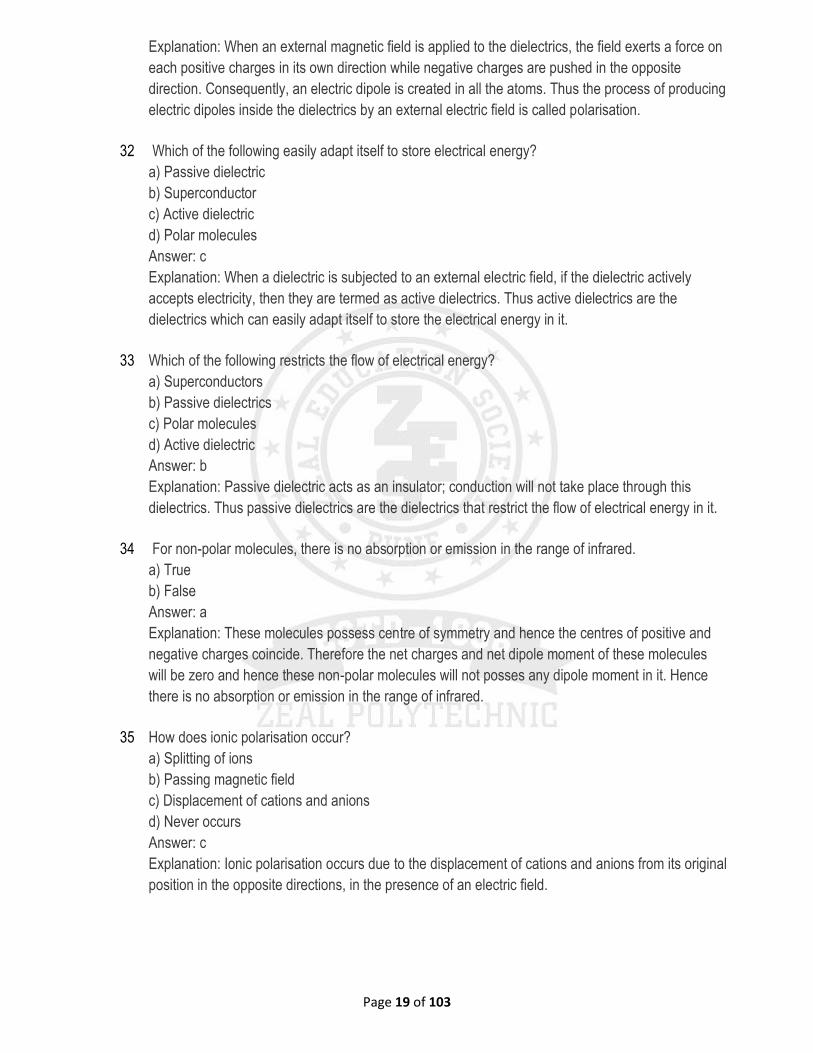
29 The following figure shows ____________
a) A dielectric Capacitor
b) Piezoelectric Material
c) Ferroelectric Capacitor
d) Ceramics Capacitor
Answer: a
Explanation: The given figure is a dielectric capacitor. The dielectric produces its own electric field
which helps in the movement of charge from one plate to the other in the capacitor.
30 Ceramics cannot be _________
a) Oxides
b) Sulfides
c) Nitrides
d) Carbides
Answer: b
Explanation: Ceramics are inorganic and nonmetallic elements such as oxides, nitrides and
carbides. Their production involves firing the constituents at high temperatures.
31 What is the process of producing electric dipoles inside the dielectric by an external electric field?
a) Polarisation
b) Dipole moment
c) Susceptibility
d) Magnetisation
Answer: a
Page 19 of 103
Explanation: When an external magnetic field is applied to the dielectrics, the field exerts a force on
each positive charges in its own direction while negative charges are pushed in the opposite
direction. Consequently, an electric dipole is created in all the atoms. Thus the process of producing
electric dipoles inside the dielectrics by an external electric field is called polarisation.
32 Which of the following easily adapt itself to store electrical energy?
a) Passive dielectric
b) Superconductor
c) Active dielectric
d) Polar molecules
Answer: c
Explanation: When a dielectric is subjected to an external electric field, if the dielectric actively
accepts electricity, then they are termed as active dielectrics. Thus active dielectrics are the
dielectrics which can easily adapt itself to store the electrical energy in it.
33 Which of the following restricts the flow of electrical energy?
a) Superconductors
b) Passive dielectrics
c) Polar molecules
d) Active dielectric
Answer: b
Explanation: Passive dielectric acts as an insulator; conduction will not take place through this
dielectrics. Thus passive dielectrics are the dielectrics that restrict the flow of electrical energy in it.
34 For non-polar molecules, there is no absorption or emission in the range of infrared.
a) True
b) False
Answer: a
Explanation: These molecules possess centre of symmetry and hence the centres of positive and
negative charges coincide. Therefore the net charges and net dipole moment of these molecules
will be zero and hence these non-polar molecules will not posses any dipole moment in it. Hence
there is no absorption or emission in the range of infrared.
35 How does ionic polarisation occur?
a) Splitting of ions
b) Passing magnetic field
c) Displacement of cations and anions
d) Never occurs
Answer: c
Explanation: Ionic polarisation occurs due to the displacement of cations and anions from its original
position in the opposite directions, in the presence of an electric field.
Page 20 of 103
36 Polar molecules have permanent dipole moments even in the absence of an electric field.
a) False
b) True
Answer: b
Explanation: In the absence of an electric field the polar molecules posses some dipole moment.
These dipoles are randomly arranged and they cancel each other. Hence the net dipole moment is
very less.
37 Which of the following polarisations is very rapid?
a) Electronic polarisation
b) Ionic polarisation
c) Space charge polarisation
d) Orientation polarisation
Answer: a
Explanation: Electronic polarisation is very rapid and will complete at the instant the voltage is
applied. The reason is that the electrons are very light particles. Therefore even for high frequency
this kind of polarisation occurs.
38 Which of the following is the slowest polarisation method?
a) Ionic polarisation
b) Orientation polarisation
c) Electronic polarisation
d) Space charge polarisation
Answer: d
Explanation: Space charge polarisation is very slow because in this case, the ions have to diffuse
over several interatomic distances. Also, this process occurs at a very low frequency.
39 When does a dielectric become a conductor?
a) At avalanche breakdown
b) At high temperature
c) At dielectric breakdown
d) In the presence of magnetic field
Answer: c
Explanation: When a dielectric is placed in an electric field and if the electric field is increased, when
the electric field exceeds the critical field, the dielectric loses its insulating property and becomes
conducting. This is called dielectric breakdown.
40 Which of the following breakdowns occur at a higher temperature?
a) Avalanche breakdown
b) Thermal breakdown
c) Electrochemical breakdown
d) Dielectric breakdown
Answer: b
Page 21 of 103
Explanation: When a dielectric is subjected to an electric field, heat is generated. This generated
heat is dissipated by the dielectric. In some cases, the generated heat will be very high compared to
the heat dissipated. Under such conditions, the temperature inside the dielectric increases and heat
may produce breakdown. This is thermal breakdown.
41 When mobility increases, insulation resistance decreases and dielectric becomes conducting.
a) True
b) False
Answer: a
Explanation: If the temperature is increased, the mobility of ions increases and hence
electrochemical reaction may be induced to take place. Therefore when the mobility of ions is
increased, insulation resistance decreases and hence dielectric becomes conducting.
42 Which of the following materials exhibit Ferro-electricity?
a) Iron
b) Platinum
c) Hydrogen
d) Rochelle salt
Answer: d
Explanation: When a dielectric exhibits electric polarisation even in the absence of an external field,
it is known as ferro-elecricity and these materials are termed as Ferro-electrics. They are
anisotropic crystals that exhibit spontaneous polarisation. Hence only Rochelle salt exhibits Ferro-
electricity.
43
Calculate the electronic polarizability of an argon atom whose ɛr = 1.0024 at NTP and N =
2.7×1025 atoms/m3.
a) 0.0024 Fm2
b) 7.87 ×10-40 Fm2
c) 7.87 Fm2
d) 1.0024×10-40 Fm2
Answer: b
Explanation: Electronic polarisabilty αe = (ε0 (εr-1))/N
Electronic polarisability = 7.87 × 10-40 Fm2.
44
Calculate the dielectric constant of a material which when inserted in parallel condenser of area
10mm × 10mm and distance of separation of 2mm, gives a capacitance of 1 -9 F.
a) 8.854×10⁻¹²
b) 100
c) 2259
d) 5354
Answer: c
Explanation: C = (εr ε0 A)/d
εr = Cd/(ε0 A) = 2259.
Page 22 of 103
45 Find the capacitance of layer of A12 O3 that is 0.5μm thick and 2000mm2 of square area εr = 8.
a) 1000μF
b) 0.283μF
c) 16μF
d) 2.83μF
Answer: b
Explanation: C = (εr ε0 A)/d
Capacitance = 0.283μF.
46 For a dielectric, the condition to be satisfied is
a) ζ/ωε > 1
b) ζ/ωε < 1
c) ζ = ωε
d) ωε = 1
Answer: b
Explanation: In a dielectric, the conductivity will be very less. Thus the loss tangent will be less than
unity. This implies ζ/ωε < 1 is true.
47 For a perfect dielectric, which parameter will be zero?
a) Conductivity
b) Frequency
c) Permittivity
d) Permeability
Answer: a
Expl nation: The conductivit will be minimum for a dielectric. For a per ect dielectric, the
conductivity will be zero.
48
Calculate the phase constant of a wave with frequency 12 rad/s and velocity 3×10⁸ m/s(in 10-
8 order)
a) 0.5
b) 72
c) 4
d) 36
Answer: c
Explanation: The phase constant is given by β = ω√(με), where ω is the frequency in rad/s and
1/√(με) is the velocity of wave. On substituting √(με) = 3×10⁸ and ω = 12, we get β = 12/(3×108) = 4
x 10-8m/s.
49 For a lossless dielectric, the attenuation will e
a) 1
b) 0
c) -1
d) Infinity
Answer: b
Page 23 of 103
Explanation: The attenuation is the loss of power of the wave during its propagation. In a lossless
dielectric, the loss of power will not occur. Thus the attenuation will be zero.
50 Calculate the velocity of a wave with frequency 2 x10⁹ rad/s and phase constant of 4 x 10⁸ units.
a) 0.5
b) 5
c) 0.2
d) 2
Answer: b
Explanation: The velocity of a wave is the ratio of the frequency to the phase constant. Thus V =
ω/β. On substitu ing t given values, we get V = 2 x10⁹/ 4 x 108 = units.
51
Which of the following is the correct relation between wavelength and the phase constant of a
wave?
a) Phase constant = 2π/wavelength
b) Phase constant = 2π x wavelength
c) Phase constant = 1/(2π x wavelength)
d) Phase constant = wavelength/2π
Answer: a
Explanation: The phase constant is the ratio of 2π to the wavelength λ. Thus β = 2π/λ is the correct
relation.
52 In lossy dielectric, the phase difference between the electric field E and the magnetic field H is
a) 90
b) 60
c) 45
d) 0
Answer: d
Explanation: In a lossy dielectric, the E and H component will be in phase. This implies that the
phase difference between E and H will be 0.
53 The intrinsic impedance is the ratio of square root of
a) Permittivity to permeability
b) Permeability to permittivity
c) Phase constant to wavelength
d) Wavelength to phase constant
Answer: b
Explanation: The intrinsic impedance is the impedance of a particular material. It is the ratio of
square root of the permeability to permittivity. For air, the intrinsic impedance is 377 ohm or 120π.
Page 24 of 103
54 Calculate the skin depth of a material with attenuation constant of 2 units.
a) 2
b) 1
c) 0.5
d) 4
Answer: c
Explanation: The skin depth of a material is the reciprocal of the attenuation constant. Thus δ = 1/α.
On substituting for α = 2, we get δ = ½ = 0.5 units.
55 Calculate the phase constant of a wave with skin depth of 2.5 units.
a) 5/2
b) 5
c) 2
d) 2/5
Answer: d
Explanation: The skin depth is the reciprocal of the phase constant and the attenuation constant
too. Thus δ = 1/β. On substituting for δ = 2.5, we get β = 1/δ = 1/2. = 2/5 units.
56 An example for lossless propagation is
a) Dielectric waveguide propagation
b) Conductor propagation
c) Cavity resonator propagation
d) It is not possible
Answer: d
Explanation: There are many techniques employed to achieve zero attenuation or maximum
propagation. But it is not achievable practically. Thus lossless propagation is not possible
practically.
57 Skin depth phenomenon is found in which materials?
a) Insulators
b) Dielectrics
c) Conductors
d) Semiconductors
Answer: c
Explanation: Skin depth is found in pure conductors. It the property of the conductor to allow a small
amount of electromagnetic energy into its skin, but not completely. This is the reason why EM
waves cannot travel inside a good conductor.
58 Which of the following is not an example of elemental solid dielectric?
a) Diamond
b) Sulphur
c) Silicon
d) Germanium
Answer: c
Page 25 of 103
Explanation: Elemental solid dielectrics are the materials consisting of single type of atoms. Such
materials have neither ions nor permanent dipoles and possess only electronic polarisation. Its
examples are diamond, sulphur and germanium.
59
Ionic non polar solid dielectrics contain more than one type of atoms but no permanent dipoles.
State True/False
a) True
b) False
Answer: a
Explanation: In ionic crystals, the total polarisation is electronic and ionic in nature. Thus, it implies
that it contains more than one type of atom and no permanent dipoles.
60 Compute the refractive index when the dielectric constant is 256 in air.
a) 2562
b) 16
c) 256
d) 64
Answer: b
Explanation: By Maxwell relation, εr = n2, where εro is the dielectric constant at optical frequencies
and n is the refractive index.For the given dielectric constant we get n = 16.
61
Dielectric property impacts the behaviour of a material in the presence of electric field. State
True/False.
a) True
b) False
Answer: a
Explanation: Based on the dielectric property, a material can be classified as piezoelectric,
ferroelectric, pyroelectric and anti-ferroelectric materials under the influence of electric field.
62 Curie-Weiss law is applicable to which of the following materials?
a) Piezoelectric
b) Ferroelectric
c) Pyroelectric
d) Anti-ferroelectric
Answer: b
Explanation: Curie-Weiss law is given by χe = εr -1 = C/(T-θ), where C is the curie constant and θ is
the characteristic temperature which is usually a few degrees higher than the curie temperature for
ferromagnetic materials.
63 Curie-Weiss law is used to calculate which one of the following?
a) Permittivity
b) Permeability
c) Electric susceptibility
d) Magnetic susceptibility
Answer: c
Page 26 of 103
Explanation: Curie-Weiss law is given by χe = εr -1. Thus it is used to calculate the electric
susceptib lity of a material.
64 Calculate the loss tangent when the dielectric constant in AC field is given by 3 + 2j.
a) (2/3)
b) (3/2)
c) (-3/2)
d) (-2/3)
Answer: d
Explanation: The AC dielectric constant is given by εr = ε` – jε“, where ε` is the real part of AC
dielectric and ε“ is the imaginary part of AC dielectric. The loss tangent is given by tan δ = ε“/ε` = -
2/3.
65 When a dielectric loses its dielectric property, the phenomenon is called
a) Dielectric loss
b) Dielectric breakdown
c) Polarisation
d) Magnetization
Answer: b
Explanation: Due to various treatments performed on the dielectric, in order to make it conduct, the
dielectric reaches a state, where it loses its dielectric property and starts to conduct. This
phenomenon is called as dielectric breakdown.
66 Choose the best definition of dielectric loss.
a) Absorption of electric energy by dielectric in an AC field
b) Dissipation of electric energy by dielectric in a static field
c) Dissipation of heat by dielectric
d) Product of loss tangent and relative permittivity
Answer: a
Explanation: In the scenario of an AC field, the absorption of electrical energy by a dielectric
material is called as dielectric loss. This will result in dissipation of energy in the form of heat.
67 Compute the loss factor when the loss tangent is 0.88 and the real part of dielectric is 24.
a) 12.12
b) 12.21
c) 21.21
d) 21.12
Answer: d
Explanation: The loss factor is nothing but the imaginary part of AC dielectric It is given by, ε“ = ε`
tan δ. We get loss factor as 24 x 0.88 = 21.12.
Page 27 of 103
68 The loss tangent refers to the
a) Power due to propagation in conductor to that in dielectric
b) Power loss
c) Cur ent loss
d) Charge loss
Answer: a
Explanation: The loss tangent is the tangent angle formed by the plot of conduction current density
vs displacement current density. It is the ratio of Jc by Jd. It represents the loss of power due to
propagation in a dielectric, when compared to that in a conductor.
69
Calculate the conduction current density when the resistivity of a material with an electric field of 5
units is 4.5 units.
a) 22.5
b) 4.5/5
c) 5/4.5
d) 9.5
Answer: c
Explanation: The conduction current density is the product of the co ductivity and the electric field.
The resistivity is the reciprocal of the conductivity. Thus the required formula is Jc = ζ E = E/ρ =
5/4.5 units.
70 At high frequencies, which parameter is sig ificant?
a) Conduction current
b) Displacement curre t
c) Attenuation constant
d) Phase constant
Answer: b
Explanation: The conduction current occurs in metals and is independent of the frequency. The
attenuation and phase constant highly depend on the varying frequency. The displacement current
occurs due to dielectrics and is significant only at very high frequencies.
71
Find the loss tangent of a material with conduction current density of 5 units and displacement
current density of 10 units.
a) 2
b) 0.5
c) 5
d) 10
Answer: b
Explanation: The loss tangent is the ratio of Jc by Jd. On substituting for Jc = 5 and Jd = 10, the
loss tangent, tan δ = 5/10 = 0.5. It is to be noted that it is tangent angle, so that the maxima and
minima lies between 1 and -1 respectively.
Page 28 of 103
72 The loss tangent is also referred to as
a) Attenuation
b) Propagation
c) Dissipation factor
d) Polarization
Answer: c
Explanation: The loss tangent is the measure of the loss of power due to propagation in a dielectric,
when compared to that in a conductor. Hence it is also referred to as dissipation factor.
73 The loss tangent of a wave propagation with an intrinsic angle of 20 degree is
a) Tan 20
b) Tan 40
c) Tan 60
d) Tan 80
Answer: b
Explanation: The angle of the loss tangent δ is t ice the intr nsic angle θn. Thus tan δ = tan 2θn =
tan 2(20) = tan 40.
74 The expression for the loss tangent is given by
a) ζ/ωε
b) ωε/ζ
c) ζ/ω
d) ω/ε
Answer: a
Explanation: The conduction current density is Jc = ζ E and the displacement current density is Jd
= jωεE. Its magnitude will be ωεE. Thus the loss tangent tan δ = Jc /Jd = ζ/ωε is the required
expression.
75 Find the loss angle in degrees when the loss tangen is 1.
a) 0
b) 30
c) 45
d) 90
An wer: c
Explanation: The loss tangent is tan δ, where δ is the loss angle. Given that loss tangent tan δ = 1.
Thus we get δ = tan-1(1) = 450.
76 The complex permittivity is given by 2-j. Find the loss tan ent.
a) 1/2
b) -1/2
c) 2
d) -2
Answ r: a
Explanation: The loss tangent for a given complex permittivity of ε = ε’ – jε’’ is given by tan δ = ε’’/ ε’.
Thus the loss tangent is 1/2.
Page 29 of 103
77 The intrinsic angle of the wave with a loss angle of 0 is
a) 120
b) 60
c) 90
d) 30
Answer:
Explanation: The angle of the loss tangent δ is twice the intrinsic angle θn. Thus tan δ = tan 2θn.
We get θn = δ/2 = 60/2 = 30 degrees.
78
What is the dielectric constant of the medium if the capacitance of a parallel plate capacitor
increases fro 40F to 80F on introducing a dielectric medium between the plates?
a) 20
b) 0.5
c) 2
d) 5
Answer: c
Explanation: Capacitance without dielectric = 40 F.
Capacitance with dielectric = 80 F.
k = 8040
k = 2.
79
How does the potential difference change with the effect of the dielectric when the battery is kept
disconnected from the capacitor?
a) Increases
b) Decreases
c) Remains constant
d) Becomes zero
Answer: b
Explanation: When the dielectric slab is introduced between the plates, the induced surface charge
on the dielectric reduces the electric field. The reduction in the electric field results in a decrease in
potential difference.
V = Ed = E0dk=V0k.
80
How does the potential difference change with the effect of the dielectric when the battery remains
connected across the capacitor?
a) Increases
b) Decreases
c) Remains constant
d) Becomes zero
Answer: c
Explanation: As the battery remains connected across the capacitor, so the potential difference
remains constant at V0 even after the introduction of the dielectric slab. In this way, dielectric has an
effect on potential difference.
Page 30 of 103
81
How does the capacitance change with the effect of the dielectric when the battery remains
connected across the capacitor?
a) Increases
b) Decreases
c) Zero
d) Remains constant
Answer: a
Explanation: When a dielectric is introduced, and the battery remains connected across the
capacitor, the capacitance increases from C0 to C.
C = kC0.
82
How does the electric field change with the effect of the dielectric when the battery remains
connected across the capacitor?
a) Increases
b) Decreases
c) Remains unchanged
d) Zero
Answer: c
Explanation: As the potential difference remains unchanged, so the electric field E0 between the
capacitor plates remain unchanged.
E = Vd = V0d = E0.
83
The charge on the capacitor plates decreases from Q0 to Q with the effect of the dielectric when the
battery remains connected across the capacitor.
a) True
b) False
Answer: b
Explanation: When a dielectric is introduced, and he battery remains connected across the
capacitor, the charge on the capacitor plates increases from Q0 to Q.
Q = CV = kC0.V0 = kQ0.
84
How does the capacitance change with the effect of the dielectric when the battery is kept
disconnected from the capacitor?
a) Increases
b) Decreases
c) Remains constant
d) Zero
Answer: a
Explanation: When the battery is disconnected, and a dielectric is introduced, there will be a
decrease in potential difference and as a result, the capacitance increases k times.
C = Q0V
C = [Q0(V0k)]
C = kQ0V0
C = kC0.
Page 31 of 103
85
In a parallel plate capacitor, the capacitance increases from 100 F to 800 F, on introducing a
dielectric medium between the plates. What is the dielectric constant of the medium?
a) 0.125
b) 125
c) 80
d) 8
Answer: d
Explanation: Capacitance with dielectric = 800 F
Capacitance without dielectric = 100 F
Dielectric constant = (CapacitancewithdielectricCapacitancewithoutdielectric)
k = (800F100F)
k = 8.
Therefore, the dielectric constant is calculated as 8.
86 Potential drop in a dielectric is equal to _______
a) Electric field strength*thickness
b) Electric field strength*area of a cross section
c) Electric field strength
d) Zero
Answer: a
Explanation: When a dielectric is introduced between the two plates of a parallel plate capacitor, the
potential difference decreases by the value of the product of electric field strength*thickness which
is the potential difference of the dielectric.
87
The electric field strength is 10N/C and the thickness of the dielectric is 3m. Calculate the potential
drop in the dielectric.
a) 10V
b) 20V
c) 30V
d) 40V
Answer: c
Explanation: The potential drop in a dielectric= electric field strength*area of cross section = 10*3 =
30V.
88
The electric fields of dielectrics having the same cross sectional area in series are related to their
relative permittivities in which way?
a) Directly proportional
b) Inversely proportional
c) Equal
d) Not related
Answer: b
Explanation: Let us consider two plates having fields E1 and E2 and relative permittivities e1 and
e2. Then, E1=Q/(e0*e1*A) and E2=Q/(e0*e2*A), where e0=absolute permittivity and A=area of
cross section. From the given expression, we see that E1/E2=e2/e1, hence the electric field is
inversely proportional to the relative permittivities.
Page 32 of 103
89 What happens to the capacitance when a dielectric is introduced between its plates?
a) Increases
b) Decreases
c) Remains the same
d) Becomes zero
Answer: a
Explanation: The capacitance of a capacitance increases when a dielectric is introduced between its
plates because the capacitance is related to the dielectric constant k by the equation:
C=k∈0A/d.
90
Calculate the relative permittivity of the second dielectric if the relative permittivity of the first is 4.
The electric field strength of the first dielectric is 8V/m and that of the second is 2V/m.
a) 32
b) 4
c) 16
d) 8
Answer:
Explanation: The relation between the two electric fields and the relative permittivities is:
E1/E1=e2/e1. Substituting the given values, we get e2=16.
91
What happens to the potential drop between the two plates of a capacitor when a dielectric is
introduced between the plates?
a) Increases
b) Decreases
c) Remains the same
d) Becomes zero
Answer: b
Explanation: When a dielectric is introduced between the two plates of a parallel plate capacitor, the
potential difference decreases because the potential difference of the dielectric is subtracted from it.
92
If the potential difference across the plates of a capacitor is 10V and a dielectric having thickness
2m is introduced between the plates, calculate the potential difference after introducing the
dielectric. The electric field strength is 2V/m.
a) 4V
b) 6V
c) 8V
d) 10V
Answer: b
Explanation: When a dielectric is introduced between the plates of a capacitor, its potential
difference decreases.
New potential difference= potential difference without dielectric-potential difference of dielectric =
10-2*2 = 6V.
Page 33 of 103
93
Calculate the capacitance if the dielectric constant=4, area of cross section= 10m2 and the
distance of separation between the plates is 5m.
a) 7.08*10-11F
b) 7.08*1011F
c) 7.08*10-12F
d) 7.08*10-10F
Answer: a
Explanation: The expression to find capacitance when a dielectric is introduced between the plates
is:
C=ke0A/d. Substituting the given values in the equation, we get C = 7.08*10-11F.
94 A dielectric is basically a ________
a) Capacitor
b) Conductor
c) Insulator
d) Semiconductor
Answer: c
Explanation: A dielectric is basically an insulator because it has all the properties of an insulator.
95
What happens to the potential difference between the plates of a capacitor as the thickness of the
dielectric slab increases?
a) Increases
b) Decreases
c) Remains the same
d) Becomes zero
Answer: b
Explanation: When a dielectric is introduced between the plates of a capacitor, its potential
difference decreases.
New potential difference= potential difference without dielectric-potential difference of dielectric.
Hence as the thickness of the dielectric slab increases, a larger value is subtracted from the original
potential difference.
96 Dielectrics which show spontaneous polarization are called as __________
a) Pyroelectric
b) Piezoelectric
c) Ferroelectric
d) Centrosymmetric
Answer: c
Explanation: The Dielectric materials which exhibit spontaneous polarization, i.e., are polarized
even in the absence of an applied electric field and whose polarization is reversible are called
ferroelectric materials.
Page 34 of 103
97 Polarization in Ferroelectric materials is ___________
a) Permanent
b) Spiked
c) Linear
d) Reversible
Answer: d
Explanation: The polarization in the ferroelectric materials is reversible. Under suitable electric field,
the polarization can be reversed as desired.
98 All ferroelectric materials are pyro electric and piezoelectric.
a) True
b) False
Answer: a
Explanation: All the ferroelectric materials are piezoelectric and piezoelectric but the reverse is not
true. Ferroelectricity can occur only in non-centro symmetric crystals, just like piezoelectricity.
99 The temperature characteristic of every ferroelectric crystal is called ________
a) Transition Temperature
b) Crystal Temperature
c) Ferro Temperature
d) Weiss Temperature
Answer: a
Explanation: Every ferroelectric curve is characterized by a temperature called Ferroelectric curie
temperature or transition temperature, above which it loses its ferroelectric behaviors and shows
Para electric behavior.
100 The dielectric constant of a ferroelectric material changes with _______
a) Frequency
b) Temperature
c) Atmospheric Pressure
d) Wavelength
Answer: b
Explanation: The dielectric constant of a ferroelectric material changes with temperature according
to the Curie-Weiss law which is given by: εr = B + C/T – Tc, where B d C are constants.
Prepared By
Badadhe P S
Verified By
Jadhav D G
Module Coordinator
Re-Verified By
Navale S N
Academic Coordinator
Approved By
Tupe S G
HoD E&Tc
Page 35 of 103
ZEAL EDUCATION SOCIETY’S
ZEAL POLYTECHNIC,PUNE
NARHE │PUNE -41 │ INDIA
DEPARTMENT OF E&Tc ENGINEERING
Question Bank for Multiple Choice Questions
03 – Magnetic Properties of Materials
Marks:-16
Content of Chapter:-
3.1 Classifications of magnetic materials, Permanent magnetic dipole , Diamagnetism, Paramagnetism
Ferromagnetism, Ferromagnetic domain
3.2Magnetisation curve, Hysteresis loop, Magnetostriction effect, Application for ultrasonic generation
permeability and affecting factors
3.3magnetic materials iron and silicon iron alloy nickel iron alloy
3.4 anti-ferromognetism and ferrimagnetism.
1 the presence of parallel alignment of magnetic dipole moment is given by which materials?
a) Diamagnetic
b) Ferromagnetic
c) Paramagnetic
d) Ferromagnetic
Answer: b
Explanation: The ferromagnetic materials are characterized by parallel alignment of magnetic dipole
moments. Their susceptibility is very large.
2 The magnetic materials follow which law?
a) Faraday’s law
b) Ampere law
c) Lenz law
d) Curie Weiss law
Answer: d
Explanation: Generally, the ferromagnetic, paramagnetic and diamagnetic materials follow the Curie
Weiss law, which relates the magnetization and the applied field.
Page 36 of 103
3
Find the internal field when the applied field is 12 units, molecular field constant is 0.1 units and the
magnetization is 74 units.
a) 86
b) 62
c) 752
d) 19.4
Answer: d
Explanation: From Curie law, the internal field of a magnetic material is given by H = Ho + χ M, where
χ is the molecular field constant. Put χ = 0.1, M = 74 and Ho = 12, we get H = 12 + (0.1)74 = 19.4 nits.
4 In which materials the magnetic anisotropy is followed?
a) Diamagnetic
b) Paramagnetic
c) Ferr magnetic
d) erromagnetic
Answer: c
Explanation: In materials like iron, the magnetic properties depend on the direction in which they are
measured. This is magnetic anisotropy. The material iron is a ferromagnetic material type.
5 Piezoelectric effect is analogous to which phenomenon?
a) Electrostriction
b) Magnetostriction
c) Anisotropy
d) Magnetization
Answer: b
Explanation: The piezoelectric effect is the mechanical strain caused on a material like quartz when
subjected to an electric field. The same is observed in a ferromagnetic material called
Magnetostriction.
6 The converse of Magnetostriction is called the
a) Magnetization
b) Magnetic anisotropy
c) Villari effect
d) Curie effect
Answer: c
Explanation: When a strain is applied, the change in magnetic field is observed. This is the converse
of the Magnetostriction phenomenon and is called Villari effect.
7 The materials having very small susceptibility at all temperatures are
a) Antiferromagnetic
b) Diamagnetic
c) Ferromagnetic
d) Paramagnetic
Answer: a
Page 37 of 103
Explanation: In antiferromagnetic materials, the susceptibility will decrease with increase in
temperature. They have relatively small susceptibility at all temperatures.
8
Find the susceptibility when the curie constant is 0.2 and the difference in critical temperature and
paramagnetic curie temperature is 0.01.
a) 2
b) 20
c) 0.02
d) 200
Answer: b
Explanation: The susceptibility in magnetic materials is given by χm = C (T-θ), where C is the curie
constant, T is the critical temperature and θ is the paramagnetic curie temperature. Put C = 0.2 and T-
θ = 0.01, thus we get susceptibility as 0.2/0.01 = 20.
9 The susceptibility is independent of temperature in which material?
a) Paramagnetic
b) Ferromagnetic
c) Diamagnetic
d) Ferromagnetic
Answer: c
Explanation: In the diamagnetic materials, the susceptibility is very small and negative. Thus the
susceptibility will be independent of the temperature. The atoms of solids having closed shells and
metals like gold have this property.
10 In ferromagnetic materials the susceptibility is infinity. State True/False
a) True
b) False
Answer: a
Explanation: The ferromagnetic materials are iron, nickel, cobalt which are highly attracted by
magnetic field. Thus their susceptibility is also very high and nearing infinity. Also ferrimagnetics have
infinite susceptibility.
11 If a material is ferromagnetic, what shall be the value of χ?
a) Negative
b) Small and positive
c) Large and Positive
d) Insufficient information
Answer: c
Explanation: When a material is ferromagnetic, the magnetic susceptibility, χ, is large and positive. For
a diamagnetic material it is negative and for a paramagnetic material, it is small and positive.
Page 38 of 103
12 Which of the following is a diamagnetic material?
a) Sodium
b) Calcium
c) Oxygen (at STP)
d) Nitrogen (at STP)
Answer: d
Explanation: Nitrogen (at STP) is a diamagnetic material. Sodium, Calcium and Oxygen (at STP) are
paramagnetic in nature.
13 Which of the following is the correct expression for Curie’s law?
a) χ = Cμ0T
b) χ = Cμ0/T
c) μ0 = C χ T
d) μ0 = C χ /T
Answer: b
Explanation: The expression, χ = Cμ0/T, is the correct expression for the Curie’s law. It shows that, for
a paramagnetic material, both χ and μ depend not only on the material, but also on the sample
temperature.
14 Curie’s law is applicable at every point on a Paramagnetic Material.
a) True
b) False
Answer: b
Explanation: As the field is increased or the temperature is lowered, the magnetization increases until
it reaches the saturation value, at which point all the dipoles are perfectly aligned with the field.
Beyond this, Curie’s law is no longer valid.
15 The phenomenon of perfect diamagnetism is called ___________
a) Superconductivity
b) Diamagnetic Effect
c) Zero Kelvin Effect
d) Meissner Effect
Answer: d
Explanation: The phenomenon of perfect diamagnetism in superconductors is called the Meissner
effect, after the name of its discoverer. It is used to magnetically levitate superfast trains.
16
Materials in which magnetization persists even after the field has been removed are called
___________
a) Diamagnetic
b) Paramagnetic
c) Soft Ferro magnets
d) Hard Ferro magnets
Answer: d
Page 39 of 103
Explanation: In Hard Ferro magnets, even after the magnetic field has been removed, the
magnetization persists. Alnico is one such material.
17 Superconductors are diamagnetic materials.
a) True
b) False
Answer: a
Explanation: Diamagnetic materials cooled to very low temperatures exhibits both perfect conductivity
and perfect diamagnetism. Here the field lines are completely expelled. They are called
superconductors.
18 Which of the following is not a constituent of Alnico?
a) Iron
b) Aluminum
c) Magnesium
d) Copper
Answer: c
Explanation: Alnico is a hard Ferro magnet. The magnetization in it persists even after the field has
been removed. It consists of iron, aluminum, cobalt, nickel and copper.
19 At high temperature a Ferro magnet becomes __________
a) Diamagnetic
b) Paramagnetic
c) Hard Ferro magnet
d) Soft Ferro Magnet
Answer: b
Explanation: The properties of a Ferro-magnet are depended on temperature. When they are heated
up to a high temperature, it loses its Ferro magnetic properties and become a paramagnet. This
transition occurs at a specific temperature, called the transition point.
24
If the number of atoms in the domain in ferromagnetic iron, in the form of a cube of side length 1μm, is
8.65 X 10¹⁰ atoms and dipole moment of each iron atom is 9.27 X 10⁻²⁴ Am2, what is the maximum
Magnetization of the domain?
a) 6 X 10⁵ A/m
b) 7 X 10⁵ A/m
c) 8 X 10⁵ A/m
d) 9 X 10⁵ A/m
Answer: c
Explanation: Now, we know the maximum dipole moment = N X m
Mmax = 8.65 X 1010 X 9.27 X 10-2
= 8 X 10-13 Am2
Vol me = (10-6)3 = 10-18 m3
Therefore, Magnetization = Mmax/ Volume
= 8 X 10-13 Am2/10-18 m3
Page 40 of 103
= 8 X 10⁵ A/m.
25 Which of the following conditions are desired in the core of an electromagnet?
a) High permeability and High retentivity
b) Low permeability and High retentivity
c) High permeability and Low retentivity
d) Low permeability and Low retentivity
Answer: c
Explanation: Ferromagnetic materials have high permeability and low retentivity. Due to these
properties, the core of electromagnets is made up of ferromagnetic materials.
26 Which of the following parameter is used to assess the magnetic ability of a material?
a) Magnetic flux density
b) Magnetization
c) Magnetic dipole moment
d) Susceptibility
Answer: d
Explanation: Magnetic susceptibility is a measure to quantify the ability of a material to undergo
magnetization in an applied magnetic field. It is the ratio of magnetization (M) to the applied magnetic
field intensity (H).
27 For a diamagnetic material, which of the following statement is correct?
a) Magnetic susceptibility < 0
b) Magnetic susceptibility > 0
c) Magnetic susceptibility = 0
d) Magnetic susceptibility = 1
Answer: a
Explanation: Diamagnetic materials are those which repel magnetic field and hence their magnetic
susceptibility (χ) is negative.
28 For a diamagnetic material, which of the following statement is correct (μr = relative permeability)?
a) μr > 2
b) μr < 1
c) μr > 1
d) μr = 1
Answer: b
Explanation: A diamagnetic material has a constant relative permeability (μr) slightly less than 1.
29 For a paramagnetic material, which of the following statement is correct?
a) Magnetic susceptibility < 0
b) Magnetic susceptibility > 0
c) Magnetic susceptibility = 0
d) Magnetic susceptibility = -1
Answer: b
Explanation: Magnetic susceptibility (χ) is very small positive quantity for a paramagnetic material.
Page 41 of 103
30 For a paramagnetic material, which of the following statement is correct (μr = relative permeability)?
a) μr = 0
b) μr < 1
c) μr > 1
d) μr < 0
Answer: c
Explanation: A paramagnetic material has a constant relative permeability (μr) slightly greater than 1.
31 What is the curie temperature of iron n kelvin scale)?
a) 2195 K
b) 495 K
c) 895 K
d) 1095 K
Answer: d
Explanation: The curie temperature of iron is about 1095K. It changes its magnetic behaviour from
ferromagnetic to paramagnetic.
32 With an increase in temperature, magnetic susceptibility of a ferromagnetic material ____________
a) Increases
b) Decreases
c) Remains constant
d) First increases and then decreases
Answer: a
Explanation: Magnetic susceptibility of a ferromagnetic material decreases with increase in
temperature.
33
With an increase in temperature, magnetic susceptibility of an anti-ferromagnetic material
____________
a) Increases
b) Decreases
c) First decreases and then increases
d) First increases and then decreases
Answer: d
Explanation: Susceptibility of an anti-ferromagnetic material is first increases and then decreases with
increase in temperature.
34 With an increase in the area of hysteresis curve, power loss will ___________
a) Increases
b) Decreases
c) First decreases and then increases
d) First increases and then decreases
Answer: a
Explanation: Power loss is directly proportional to the area of hysteresis curve.
Page 42 of 103
35 Magnetic Bubbles are used as __________
a) Storage device
b) Strain gauge
c) Thermostat
d) Potentiometer
Answer: a
Explanation: Magnetic bubbles are small magnetized areas used as storage devices (data bites). One
good thing about magnetic bubbles are they do not disappear when power is turned off.
36 What will happen with magnetic materials is kept in an external magnetic field?
a) They will move
b) They will develop magnetic lines of force
c) They will create a permanent magnetic moment
d) They will be unaffected
Answer: c
Explanation: Magnetic materials are the materials which can behave like magnets. When these
materials are kept in an external magnetic field, they will create a permanent magnetic moment in it.
37 Magnetism originates due to rotational motion of charged particles.
a) True
b) False
Answer: a
Explanation: Magnetism originates from a magnetic moment of the magnetic materials due to the
rotational motion of the charged particles. When an electron revolves around the positive nucleus,
orbital magnetic moment arises.
38
What is the name of the continuous curve in the magnetic field, the tangent of which gives the
direction of magnetic intensity?
a) Magnetic lines of force
b) Magnetic lines of induction
c) Magnetic force
d) Magnetic dipole moment
Answer: a
Explanation: Magnetic lines of force are defined as the continuous curve in a magnetic field. The
tangent drawn at any point on the curve gives the direction of the resultant magnetic field at that point.
39 What is the name of the magnetic lines which forms a closed path?
a) Magnetic lines of force
b) Magnetic force between two poles
c) Magnetic field
d) Magnetic lines of induction
Answer: d
Explanation: The magnetic lines of force which originate from North Pole to South Pole doesn’t end
there itself. They are supposed to continue through the magnet and reach the North Pole from where
they started and forms a closed loop. Such lines are called magnetic lines of induction.
Page 43 of 103
40 How is the residual magnetism from material removed?
a) Retentivity
b) Coercivity
c) Magneton
d) Switching off the magnetic field
Answer: b
Explanation: The residual magnetism can be completely removed from the material by applying a
reverse magnetic field. Hence coercivity of magnetic material is the strength of the reverse magnetic
field which is used to completely demagnetise the material.
41 In which of the following magnetic moment is zero?
a) Dia-magnetic material
b) Parra-magnetic material
c) Ferromagnetic material
d) Ferrimagnetic material
Answer: a
Explanation: In a diamagnetic material, the electron orbits are more or less random, and mostly all the
magnetic moments are cancelled. Similarly, all the spins are almost paired. Hence the net magnetic
moment in the diamagnetic material is zero.
42 Which of the following is a weak magnet?
a) Ferromagnetic material
b) Antiferromagnetic
c) Paramagnetic
d) Diamagnetic
Answer: d
Explanation: The diamagnets are called weak magnets because there is no permanent dipole
moment. Their net magnetic moment is zero.
43 When does a diamagnetic material become normal material?
a) At critical temperature
b) Above critical temperature
c) Never
d) Below critical temperature
Answer: d
Explanation: Critical temperature is the temperature at which properties like magnetism changes.
When the temperature is less than the critical temperature, diamagnetic material becomes a normal
magnet.
44 Magnetic susceptibility is negative for paramagnetic material.
a) True
b) False
Answer: b
Explanation: Magnetic susceptibility is positive for paramagnetic material. It is given by Curie-Weiss
Page 44 of 103
law, Susceptibility = C/(T-θ)
Where C = Curie constant
T = Absolute temperature
θ = Curie temperature.
45 When does a paramagnetic material become diamagnetic material?
a) At critical temperature
b) Above critical temperature
c) Below critical temperature
d) Never
Answer: c
Explanation: Critical temperature is the temperature at which properties like magnetism changes.
When the temperature is less than the critical temperature, the diamagnetic material becomes a
normal magnet
46 What is the property of magnetic materials?
a) Resistivity
b) Conductivity
c) Permeability
d) Ductility
Answer: c
Explanation: There are many properties of magnetic materials, and permeability is one among them.
The other 3 properties are related to other materials like conducting and insulating materials.
47 What is the property of permeability in magnetic materials?
a) how easily the magnetic flux is broken/clear
b) how easily the magnetic flux is set up
c) how long the magnetic flux takes to form
d) how long the magnetic flux takes to clear
Answer: b
Explanation: The basic operation of magnetic material is to form magnetic flux. Permeability is the
ability of the material to determine how easily the magnetic flux is set up.
48 What is the representation of permeability?
a) coercivity/retentivity
b) flux/flux density
c) magnetic force/magnetic flux density
d) magnetic flux density/magnetic force
Answer: d
Explanation: Permeability is the property which deals, with the relationship with magnetic flux density
and magnetic force. Magnetic force/Magnetic flux density deals with the reciprocal of permeability.
Coercivity/Retentivity deals with the terms of B-H curve.
Page 45 of 103
49 How should the permeability and number of ampere turns for good magnetic materials be?
a) high permeability, high ampere turns
b) high permeability, low ampere turns
c) low permeability, low ampere turns
d) low permeability, high ampere turns
Answer: b
Explanation: High permeability is always required in magnetic materials for its good operation. At the
same time high permeability leads to less ampere turns in the materials.
49 Is retentivity associated with B-H curve?
a) Yes
b) No
Answer: a
Explanation: B-H curve deals with the concepts of retentivity and coercivity. The property of retentivity
can be shown in the B-H curve by an increasing curve in the curve.
50 What is the property of retentivity in magnetic materials?
a) After removal of external magnetic fields, magnetization exists
b) After removal of external magnetic fields, magnetization doesn’t exist
c) After removal of internal magnetic fields, magnetization exists
d) After removal of internal magnetic fields, magnetization doesn’t exist
Answer: a
Explanation: Magnetic materials have the property of retentivity in which the magnetic flux produced
acts according to the external magnetic field. When the external field is removed, the magnetization in
the materials doesn’t deform immediately.
51 What is coercively force in magnetic materials?
a) The force required to add upon the existing magnetization
b) The force required to remove the existing magnetization
c) The force required to produce magnetic flux
d) The force required to break magnetic flux
Answer: b
Explanation: Magnetic materials generally have the property of retaining magnetization, even if the
external magnetic field is removed. So, coercive force is the force that is required to reduce the
magnetization.
52 What are magnetic hard materials?
a) High retentively, low coercively
b) High retentively, high coercively
c) Low retentively, low coercively
d) Low retentively, high coercively
Answer: b
Explanation: High retentively is required for protecting the magnetic materials from losing its magnetic
property. High coercively is required to reduce the effect of retentively to protect the material.
Page 46 of 103
53 What is reluctance in magnetic materials?
a) Allows the buildup of magnetic flux
b) Reduces the buildup of magnetic flux
c) Resists the buildup of magnetic flux
d) Increases the buildup of magnetic flux
Answer: c
Explanation: Reluctance, as the name suggests, is something which is reluctant or hesitant to do. As
per the magnetic terms it resists the building up of magnetic flux in the materials.
54 High Reluctance affects the performance of magnetic materials.
a) True
b) False
Answer: a
Explanation: High reluctance means the materials resist in building up the magnetic flux to a higher
extent. So, for the proper functioning the reluctance values should be as low as possible.
55 What is the unit of reluctance in magnetic materials?
a) Henry/m
b) Weber/m2
c) Ampere-turns/Weber
d) Ampere-turns/m
Answer: c
Explanation: Henry/m deals with the unit of permeability. Weber/m2 deals with the unit of magnetic
field. Reluctance is the opposite of permeance.
56 How many classifications of magnetic materials are present?
a) 3
b) 4
c) 5
d) 6
Answer: c
Explanation: There are basically 4 properties in magnetic materials and 5 classifications. They are
diamagnetic, paramagnetic, ferromagnetic, antiferromagnetic, ferrimagnetic.
57 What is the property of ferromagnetic materials?
a) Negative magnetization
b) Magnetization slightly less than 1
c) Magnetization slightly greater than 1
d) Magnetization very much higher than 1
Answer: d
Explanation: Negative magnetization denotes the property of Diamagnetic materials. Magnetization
slightly greater than 1 denotes the property of Paramagnetic materials. Ferromagnetic materials have
magnetization in the range of 1000+.
Page 47 of 103
58 What is the example of diamagnetic materials?
a) Quartz
b) Pyrite
c) Montmorillonite
d) Biotite
Answer: a
Explanation: The other 3 materials are paramagnetic in nature, which means magnetization is slightly
above 1. Quartz is a diamagnetic material in which the magnetization is negative.
59 What is the example of ferromagnetic materials is?
a) Magnetite
b) Hematite
c) Nickel
d) Biotite
Answer: a
Explanation: Hematite denotes the example of antiferromagnetic materials. Nickel denotes an
example of ferromagnetic materials. Biotite denotes the example of paramagnetic materials.
60 Identify the expression for magnetic induction from the following.
a) B = μo(H+I)
b) B = μo(H×I)
c) B = μo(H-I)
d) B = μo(HI)
Answer: a
Explanation: Magnetic induction (B) is defined as the number of magnetic lines of induction crossing
per unit area normally through the magnetic substance, and is given by:
B = μo(H+I)
The SI unit of magnetic induction is Tesla (T).
61 Which among the following is true about magnetic susceptibility?
a) It is the ratio of magnetic intensity to intensity of magnetization
b) The SI unit of magnetic susceptibility is Tesla (T)
c) It is the ratio of intensity of magnetization to magnetic intensity
d) It is the ratio of magnetic moment to volume
Answer: c
Explanation: Magnetic susceptibility of a magnetic substance is defined as the ratio of the intensity of
magnetization (I) to the magnetic intensity (H). The expression is given by:
χm=IH
Magnetic susceptibility measures the aptness of a magnetic substance to acquire magnetism. It is a
unit less constant of magnetic substance.
Page 48 of 103
62 Pick out the unit of magnetic permeability.
a) TmA
b) TmA
c) TmA
d) AmT
Answer: b
Explanation: Magnetic permeability (μ) of a magnetic substance is defined as the ratio of its magnetic
induction (B) to the magnetic intensity (H). The expression for magnetic permeability is given as:
μ=BH
Magnetic permeability is the ability of a magnetic substances to permit magnetic field lines to pass
through it. The SI unit for this quantity is TmA.
63 Relative magnetic permeability is unit less.
a) True
b) False
Answer: a
Explanation: Yes, relative magnetic permeability is a unit less constant of magnetic substance.
Relative magnetic permeability (μr) of a magnetic substance is defined as the ratio of its magnetic
permeability to the permeability of free space. The expression for it is given as:
μr=μμo
64 The relative permeability of a medium is 0.050. What is its magnetic susceptibility?
a) 500
b) 501
c) 49.9
d) 499
Answer: d
Explanation: Given: relative permeability (μr) = 500
Required equation ➔ μr = 1+χm
χm = μr – 1
χm = 500 – 1
χm = 499
Therefore, the value of magnetic susceptibility is 499.
65
The magnetic susceptibility of a paramagnetic material at -800C is 0.0085, then what is its value at -
1800C?
a) 0.015
b) 0.016
c) 0.017
d) 0.018
Answer: c
Explanation: Given: χm1 = 0.0085; T1 = -800 C = -80 + 273 = 193 K; T2 = -1800 C = -180 + 273 = 93
K
χm ∝ 1T
Page 49 of 103
χm2χm1=T1T2
χm20.0085=19393
χm2 = 193×0.008593
χm2 = 0.017
66
A material has a permeability of 0.1 H/m when the magnetic intensity is 70 A/m. What will be the
magnetic induction inside the material?
a) 7 T
b) 0.7 T
c) 70 T
d) 0.07
Answer: a
Explanation: Given: permeability (μo) = 0.1 H/m; Magnetic intensity (H) = 70 A/m
Required equation ➔ Magnetic induction (B) = μo × H
B = 0.1 × 70
B = 7 T
Therefore, the magnetic induction inside the material is 7 T.
67 Ferromagnetic materials does not show hysteresis.
a) True
b) False
Answer: b
Explanation: Ferromagnetic materials do show hysteresis. When a ferromagnetic material is
magnetized in one direction, it will not relax back to zero magnetization when the imposed
magnetizing field is removed. The phenomenon of hysteresis in ferromagnetic materials is the result of
two effects ➔ rotation of magnetization and changes in size or number of magnetic domains.
68
Find the correct combination regarding relative permeability and magnetic susceptibility of a
paramagnetic substance.
a) μr > 1, χ < 0
b) μr < 1, χ > 0
c) μr < 1, χ < 0
d) μr > 1, χ > 0
Answer: d
Explanation: The correct combination for paramagnetic substances is given as follows:
μr > 1, χ > 0
Paramagnetic materials have a small and positive value of magnetic susceptibility (χ). The relative
permeability (μr) of paramagnetic materials is just greater than 1.
69 The hysteresis loss in soft magnetic materials must be kept ______
a) High
b) Minimum
c) Zero
d) Unaltered
Answer: b
Page 50 of 103
Explanation: Soft magnetic materials are used in cases where regular reversal of magnetization path
is required. The hysteresis losses in such materials must be kept to a minimum. This is due to a
smaller hysteresis area
70 The supermaloy primarily composed of ________________
a) Nickel
b) Iron
c) Cobalt
d) Copper
Answer: a
Explanation: Permalloy is a magnetic material invented by the scientist Gustav Elmen. It is composed
of just about 80% nickel and 5% molybdenum. It has a high relative permeability of 105.
71 Which of the following is an example of soft magnetic material?
a) Permalloy
b) Strontium
c) Alnico
d) Neodymium
Answer: a
Explanation: Permalloy is a soft magnet mainly used in electrical and electronic applications. It is
composed of roughly 45% nickel. It has a high relative permeability of around 2700.
72 What is the relative permeability of iron?
a) 250
b) 1500
c) 2700
d) 100,000
Answer: a
Explanation: Relative permeability is the measure of the effective permeability of a material.
Commercial iron has a relative permeability of 250. The values of relative permeability of Fe-Si,
permalloy, and supermaloy are 1500, 2700, and 100000 in that order.
73 The heat treatment of alnico alloys at _____ results in phase separation.
a) 100oC
b) 200oC
c) 400oC
d) 800oC
Answer: d
Explanation: Some materials are heat treated in a magnetic field to enhance their properties. At just
about 800oC, alnico undergoes a phase separation into two phases having different compositions and
amount of magnetizations.
Page 51 of 103
74 What is the hysteresis loss of permalloy?
a) 500
b) 120
c) 40
d) 21
Answer: b
Explanation: Hysteresis loss of soft magnetic materials is generally kept low due to the small area.
This value resides at 120 J m-3 for permalloy and even lower at 21 J m-3 for supermaloy.
75 Which of the following is a property of a hard magnetic material?
a) Low hysteresis
b) Low eddy loss
c) Low coercive force
d) High residual induction
Answer: d
Explanation: Hard magnetic materials are used to produce permanent magnets. These permanent
magnets have a high residual induction and large coercive force. Low hysteresis and Low eddy loss
are properties of soft magnetic materials.
76 A _____ cooling rate solidifies metallic glass made from iron- base alloys.
a) 10oC s-1
b) 100oC s-1
c) 1000oC s-1
d) 10000oC s-1
Answer: d
Explanation: Metallic glasses produced from iron-base alloys are used to provide a reduction in core
losses. When such an alloy is cooled at 104oC s-1, it solidifies into a ribbon-shaped metallic glass
instead of crystallizat
77 Which of the following is not a use of magnesium-manganese ferrites?
a) Microwave isolator
b) Gyrators
c) Wires
d) Memory core of computer
Answer: c
Explanation: Magnesium-manganese ferrites having high resistivity are used as microwave insulators
and gyrators in the KHz and MHz range. They are also used in memory cores of the computer when
there is higher manganese to magnesium ratio.
78 Yttrium-iron-garnet is used as microwave isolators in the ____ range.
a) KHz
b) MHz
c) GHz
d) THz
Answer: c
Page 52 of 103
Explanation: Garnets such as Y3Fe5O12 (yttrium-iron-garnet)have a narrow resonance line width.
These are popularly used as microwave isolators in the GHz range.
79 What is the coercive force of high carbon steel?
a) 3.98
b) 5.57
c) 18.31
d) 60
Answer: a
Explanation: Coercive force is defined as the ability of a material to withstand a magnetic field. It is
denoted by Hc and must be larger for permanent magnets (hard magnetic material). High carbon steel
has a coercive force of 3.98 kA m-1.
80 What is the value of residual induction of alnico alloys?
a) 0.9
b) 0.95
c) 1.0
d) 0.8-1.2
Answer: c
Explanation: Alnico is a common hard magnetic material containing aluminum, nickel, and cobalt (Al-
Ni-Co). It has a residual induction (Br) of 0.8 to 1.2 Wb m-2 and a coercive force (Hc) of 60-12 kA m-1.
81 If a material is paramagnetic, what shall be the value of χ?
a) Negative
b) Small and positive
c) Large and Positive
d) Depends on other factors
Answer: b
Explanation: When a material is paramagnetic, the magnetic susceptibility, χ, is small and positive. For
a diamagnetic material it is negative and for a ferromagnetic material, it is large and positive.
82 The vertical plane containing the earth’s axis of rotation is called as _____________
a) Geographic meridian
b) Magnetic Meridian
c) Magnetic Declination
d) Prime Meridian
Answer: a
Explanation: The vertical plane containing the longitude circle and the axis of rotation of the earth is
called the geographic meridian. The plane passing through north pole and south pole is called
magnetic meridian.
Page 53 of 103
83 Where would the declination be greater?
a) India
b) Africa
c) Egypt
d) Arctic
Answer: d
Explanation: The magnetic declination is greater at higher latitudes and smaller near the equator.
Thus, it would be greater in the Arctic region and smaller near equator.
84 In case of diamagnetic materials, M and H are opposite in direction.
a) True
b) False
Answer: a
Explanation: It is due to the fact that M and H are opposite in direction in a diamagnetic material that
the magnetic susceptibility for diamagnetic materials is small and negative.
85 How is the magnetic field, B, related to Magnetization, M?
a) B ∝ M
b) B ∝ 1/M
c) B ∝ M2
d) B ∝ 1/M2
Answer: a
Explanation: The Magnetic Field, B, is directly proportional to the Magnetization, M, of the material.
The true expression is: B = μ0M.
86 The dimensions of χ are ____________
a) [AL]
b) [AL2T-1]
c) [AM2L4T]
d) Dimensionless
Answer: d
Explanation: χ is a dimensionless quantity and is called the magnetic susceptibility. It is used to
identify the magnetic property of the material.
87 For a paramagnetic material, χ does not depend on Temperature.
a) True
b) False
Answer: b
Explanation: For a paramagnetic material, bot the magnetic susceptibility and the permeability
depend not only on the material but also on the sample temperature.
Page 54 of 103
88
A solenoid carry a current of 2A. If the number of turns is 1000 per meter, what is the Magnetic
Intensity?
a) 1000 A/m
b) 2000 A/m
c) 3000 A/m
d) 4000 A/m
Answer: b
Explanation: The field H is dependent on the material of the core and is
H = nI
= 1000 X 2
= 2000 A/m.
89
A solenoid has a core of a material with relative permeability 400. The windings are insulated from the
core and the magnetic Intensity is 1500 A/m. What is the Magnetization of the core?
a) 0.25 T
b) 0.50 T
c) 0.75 T
d) 1.00 T
Answer: c
Explanation: The Magnetic field, B, is given by
B = μr μ0 H
= 400 X 4π X 10-7 X 1500
= 0.75 T.
91
If for a material, the magnetization is 8 X 10⁵ A/m and the relative permeability is 200, what is the
Magnetic Intensity?
a) 4.89 X 10³ A/m
b) 4.64 X 10³ A/m
c) 4.43 X 10³ A/m
d) 4.02 X 10³ A/m
Answer: d
Explanation: Magnetization is given by: M = (μr – 1) H
8 X 105 = 199 X H
H = 4.02 X 10³ A/m.
92 The earth’s magnetic field at the equator is approximately 0.4 G. What is the earth’s dipole moment?
a) 0.8 X 10²³ Am2
b) 1.0 X 10²³ Am2
c) 1.2 X 10²³ Am2
d) 1.5 X 10² Am2
Answer: b
Explanation: We know, BE = μ0m4πr3
Given that, BE = 0.4 G = 4 X 10⁻⁵ T. For r, we take the radius of the earth 6.4 X 10⁶ m.
Hence, m = 4 X 10-5 X (6.4 X 106)3 X 4π/μo
= 1.0 X 10²³ Am2.
Page 55 of 103
93
If the magnetic meridian of a certain pla e, the horizontal component of the earth’s magnetic field is
0.26 G and the dip angle is 60°, what is the magnetic field of earth at this location?
a) 0.52 G
b) 0.46 G
c) 0.78 G
d) 0.94 G
Answer: a
Explanation: It is given that, HE = 0.26 G. Thus, we have
cos60° = HE/BE
BE = HE/ cos60°
= 0.26 X 2
= 0.52 G.
94 If the relative permeability of material lies between zero and one, the material is ____________
a) Diamagnetic Material
b) Paramagnetic Material
c) Ferromagnetic Material
d) Insufficient Information
Answer: a
Explanation: The given material is diamagnetic material. For a diamagnetic material, it’s magnetic
susceptibility is small and negative while it’s relative permeability is small and positive as μr = 1 + χ.
95 Core of electromagnets are made up of ____________
a) Diamagnetic Material
b) Paramagnetic Material
c) Ferromagnetic Material
d) Plastic
Answer: c
Explanation: Ferromagnetic materials have high permeability and low retentivity. Due to these
properties, the core of electromagnets is made up of ferromagnetic materials.
96 In which of the following the magnetic moments align themselves parallel to each other?
a) Paramagnetic material
b) Ferromagnetic material
c) Ferrimagnetic material
d) Diamagnetic material
Answer: b
Explanation: In a ferromagnetic material, the number of unpaired electrons is more. Most of these spin
magnetic moments point in one direction. Hence even in the absence of an external field, the
magnetic moments align themselves parallel to each other and give rise to a magnetic field.
Page 56 of 103
97 When does a ferromagnetic material become paramagnetic material?
a) At Curie temperature
b) Below Curie temperature
c) Above Curies temperature
d) Never
Answer: c
Explanation: Curie temperature is the temperature at which the magnetic properties of a material
change. When the temperature is greater than curie temperature, ferromagnetic material becomes
paramagnetic material.
98 Which of the following materials have a permanent magnetic moment?
a) Ferromagnetic material
b) Ferrimagnetic material
c) Diamagnetic material
d) Paramagnetic material
Answer: a
Explanation: In a ferromagnetic material, there will be a large number of unequal electron spins and
hence there exists an enormous amount of permanent magnetic moment.
99 In which of the following increases and then decreases?
a) Ferromagnetic material
b) Antiferromagnetic material
c) Paramagnetic material
d) Diamagnetic material
Answer: b
Explanation: The susceptibility is very small and is positive. It is given by, susceptibility = C/(T+θ) for
T>TN. Where TN is the Neel temperature.
Initially, the susceptibility increases slightly as the temperature increases and beyond a particular
tem erature, known as Neel temperature, the susceptibility decreases with temperature.
100 What is the material used in two port device?
a) Ferro magnets
b) Ferrites
c) Antiferromagnetism
d) Paramagnets
Answer: b
Explanation: The ferrites have low hysteresis loss and eddy current loss. Hence they are used in two
port devices such as gyrator, circulator and isolator.
Prepared By
Badadhe P S
Verified By
Jadhav D G
Module Coordinator
Re-Verified By
Navale S N
Academic Coordinator
Approved By
Tupe S G
HoD E&Tc
Page 57 of 103
ZEAL EDUCATION SOCIETY’S
ZEAL POLYTECHNIC,PUNE
NARHE │PUNE -41 │ INDIA
DEPARTMENT OF E&Tc ENGINEERING
Question Bank for Multiple Choice Questions
04 – Semiconductor Materials
Marks:-16
Content of Chapter:-
4.1 Energy bands of solids , Conductors Semiconductors,
4.2Types of semiconductors Intrinsic material Impurity type and material for various impurities
4.3 Diffusion hall effect: Thermal and electrical conductivity of semiconductor
4.4 materials for fabrication of semiconductor devices passive materials and process materials Substrate metal
capacitance material junction coating device potting packaging
1 How does a semiconductor behave at absolute zero?
a) Conductor
b) Insulator
c) Semiconductor
d) Protection device
Answer: b
Explanation: A semiconductor is a solid which has the energy band similar to that of the insulator. It
acts as an insulator at absolute zero.
2 Semiconductor acts as an insulator in the presence of impurities.
a) True
b) False
Answer: b
Explanation: When the temperature is raised or when an impurity is added, their conductivity
increases. Conductivity is inversely proportional to temperature.
3 How is the resistance of semiconductor classified?
a) High resistance
b) Positive temperature co-efficient
c) Negative temperature co-efficient
d) Low resistance
Answer: c
Explanation: Semiconductors have negative temperature co-efficient. The reason for this is, when
the temperature is increased, a large number of charge carriers are produced due to the breaking of
covalent bonds and hence these electrons move freely and gives rise to conductivity.

Page 58 of 103
4 What are the charge carriers in semiconductors?
a) Electrons and holes
b) Electrons
c) Holes
d) Charges
Answer: a
Explanation: In conductors, electrons are charge carriers. But in semiconductors, both electrons and
holes are charge carriers and will take part in conduction.
5 Which of the following is known as indirect band gap semiconductors?
a) Germanium
b) Nickel
c) Platinum
d) Carbon
Answer: a
Explanation: The elemental semiconductor is made up of a single element from the fourth column
elements such as Germanium. Here recombination takes place takes place via traps. It is called
indirect band gap semiconductors.
6 Which column elements are combined to make compound semiconductors?
a) First and fourth
b) Fifth and sixth
c) Second and fourth
d) Third and fifth
Answer: d
Explanation: The compound semiconductors are made by combining the third and fifth column
elements. Such as GaAs are made by combining third and fifth column elements.
7 Compound semiconductors are also known as direct band gap semiconductors.
a) True
b) False
Answer: a
Explanation: In compound semiconductors, recombination takes place directly and its energy
difference is emitted in the form of photons in the visible or infrared range. Hence the compound
semiconductors are also known as direct band gap semiconductors.
8 How are charge carriers produced in intrinsic semiconductors?
a) By pure atoms
b) By electrons
c) By impure atoms
d) By holes
Answer: c
Explanation: Impure semiconductors in which the charge carriers are produced due to impurity
atoms are called extrinsic semiconductors. They are obtained by doping an intrinsic semiconductor
with impurity atoms.
Page 59 of 103
9
What type of material is obtained when an intrinsic semiconductor is doped with pentavalent
impurity?
a) N-type semiconductor
b) Extrinsic semiconductor
c) P-type semiconductor
d) Insulator
Answer: a
Explanation: N-type semiconductor is obtained by doping an intrinsic semiconductor with
pentavalant impurity atoms.
10 What type of material is obtained when an intrinsic semiconductor is doped with trivalent impurity?
a) Extrinsic semiconductor
b) Insulator
c) N-type semiconductor
d) P-type semiconductor
Answer: d
Explanation: P-type semiconductor is obtained by doping an intrinsic semiconductor with trivalent
impurity.
11 What is the energy level below which all levels are completely occupied at Zero Kelvin called?
a) Boson Energy
b) Fermi Energy
c) Stable Energy
d) Ground Energy
Answer: b
Explanation: Fermi energy is said to be the energy of the highest possible occupied energy level at
0 K. Below this level, all the states are completely occupied.
12 What are the current carriers in semiconductors?
a) Electrons and Protons
b) Electrons and Nucleons
c) Electrons and Photons
d) Electrons and Holes
Answer: d
Explanation: Electrons and holes are the two current carriers in semiconductors. Electrons are
negatively charged while holes are positively charged. Their movement gives rise to a current in the
semiconductor.
13 The concentration of doping is kept below ______________
a) 1 %
b) 5 %
c) 10 %
d) 50 %
Answer: a
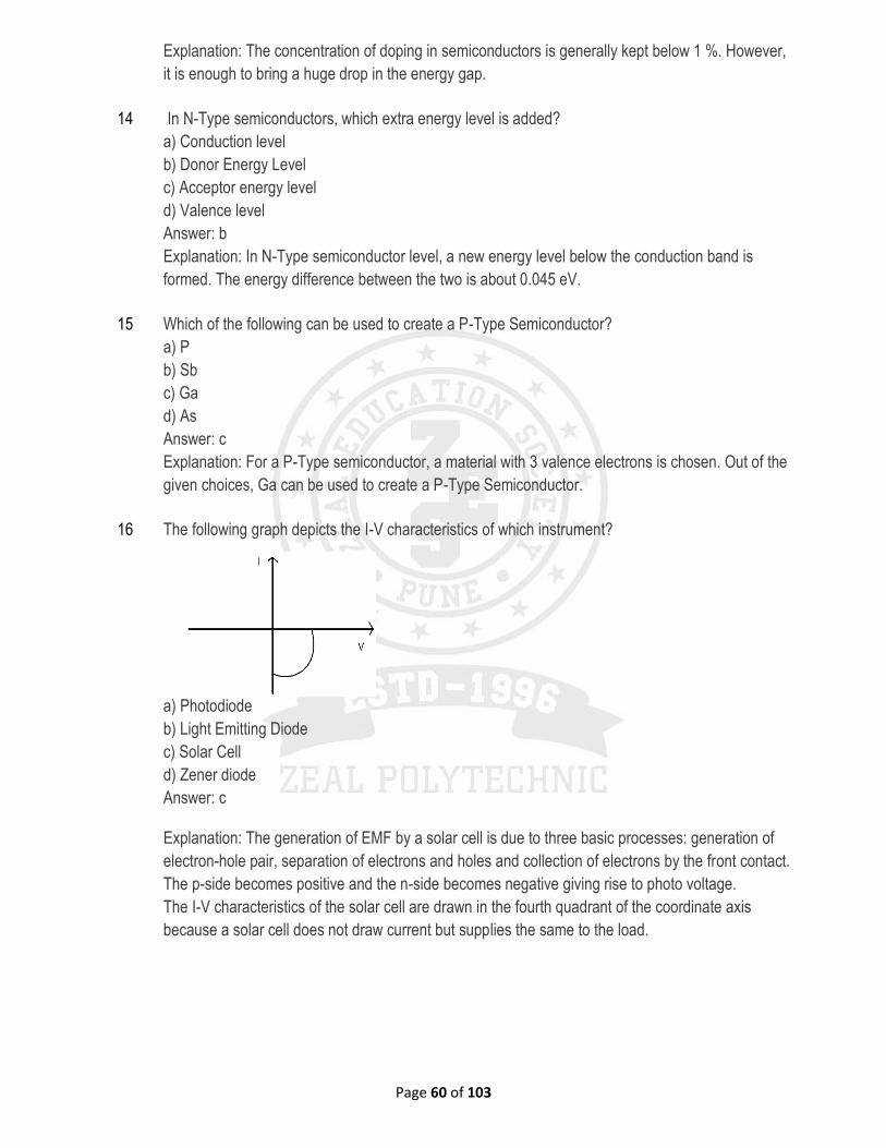
Page 60 of 103
Explanation: The concentration of doping in semiconductors is generally kept below 1 %. However,
it is enough to bring a huge drop in the energy gap.
14 In N-Type semiconductors, which extra energy level is added?
a) Conduction level
b) Donor Energy Level
c) Acceptor energy level
d) Valence level
Answer: b
Explanation: In N-Type semiconductor level, a new energy level below the conduction band is
formed. The energy difference between the two is about 0.045 eV.
15 Which of the following can be used to create a P-Type Semiconductor?
a) P
b) Sb
c) Ga
d) As
Answer: c
Explanation: For a P-Type semiconductor, a material with 3 valence electrons is chosen. Out of the
given choices, Ga can be used to create a P-Type Semiconductor.
16 The following graph depicts the I-V characteristics of which instrument?
a) Photodiode
b) Light Emitting Diode
c) Solar Cell
d) Zener diode
Answer: c
Explanation: The generation of EMF by a solar cell is due to three basic processes: generation of
electron-hole pair, separation of electrons and holes and collection of electrons by the front contact.
The p-side becomes positive and the n-side becomes negative giving rise to photo voltage.
The I-V characteristics of the solar cell are drawn in the fourth quadrant of the coordinate axis
because a solar cell does not draw current but supplies the same to the load.
Page 61 of 103
17
The Hall coefficient of a specimen is 3.66 x 10⁻⁴ m3C-1. If it’s resistivity is 8.93 x 10⁻³ Ωm, what will
be its mobility?
a) 0.01 m2V-1s-1
b) 0.02 m2V-1s-1
c) 0.03 m2V-1s-1
d) 0.04 m2V-1s-1
Answer: d
Explanation: We know, Mobility = Hall coefficient/resistivity
Therefore, Mobility = 3.66 x 10⁻⁴/8.93 x 10-3
= 0.04 m2V-1s-1.
18 Which one of the following is not an intrinsic semiconductor?
a) Carbon
b) Silicon
c) Germanium
d) Lead
Answer: a
Explanation: There are 4 bonding electrons in all the above materials. However, the energy required
to take out an electron will be maximum for carbon as the valence electrons are in the second orbit.
Hence, the number of free electrons for conduction is negligibly small in C.
19 Which of the following is n-type semiconductor?
a) CaO
b) MgO
c) ZnO
d) BaO
Answer: c
Explanation: II-VI semiconductors are generally p-type semiconductors except for ZnO and ZnTe. II-
VI semiconductors are those which contain atoms of materials that have 2 valence electrons and 6
valence electrons.
20 P-Type semiconductor has a lower electrical conductivity than N-Type semiconductor.
a) True
b) False
Answer: a
Explanation: Due to comparatively lower mobility of holes than electrons for the same level of doing
as in an N-Type semiconductor, it has lower electrical conductivity.
21
Pure Si at 300 K has equal electron (ni) and hole concentration (p) of 1.5 X 10¹⁶ m-3. Doping by
indium increases p to 4.5 X 10²² m-3. What is n in the doped silicon?
a) 4.5 X 10⁹ m-3
b) 4.5 X 10²² m-3
c) 5 X 10⁹ m-3
d)5 X 10²² m-3
Answer: c
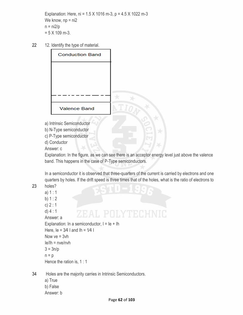
Page 62 of 103
Explanation: Here, ni = 1.5 X 10¹⁶ m-3, p = 4.5 X 10²² m-3
We know, np = ni2
n = ni2/p
= 5 X 10⁹ m-3.
22 12. Identify the type of material.
a) Intrinsic Semiconductor
b) N-Type semiconductor
c) P-Type semiconductor
d) Conductor
Answer: c
Explanation: In the figure, as we can see there is an acceptor energy level just above the valence
band. This happens in the case of P-Type semiconductors.
23
In a semiconductor it is observed that three-quarters of the current is carried by electrons and one
quarters by holes. If the drift speed is three times that of the holes, what is the ratio of electrons to
holes?
a) 1 : 1
b) 1 : 2
c) 2 : 1
d) 4 : 1
Answer: a
Explanation: In a semiconductor, I = Ie + Ih
Here, Ie = 3⁄4 I and Ih = 1⁄4 I
Now ve = 3vh
Ie/Ih = nve/nvh
3 = 3n/p
n = p
Hence the ration is, 1 : 1
34 Holes are the majority carries in Intrinsic Semiconductors.
a) True
b) False
Answer: b
Page 63 of 103
Explanation: A pure semiconductor is called an intrinsic semiconductor. Hence, in this case, the
number of electrons and holes are same, as the electron that moves out of its position leaves a hole
behind. Hence, the concentration of holes and electrons is the same in an intrinsic semiconductor.
35
If the number of electrons (majority carrier) in a semiconductor is 5 X 10²⁰ m-3 and μe is 0.135
mho, find the resistivity of the semiconductor.
a) 0.0926 Ωm
b) 0.0945 Ωm
c) 0.0912 Ωm
d) 0.0978 Ωm
Answer: a
Explanation: We know, Conductivity, ζ = ene μe
= 5 X 1.6 X 0.135 X 10 mho/m
= 10.8 mho/m
Resistivity = 1/ζ
= 0.0926 Ωm.
36
Which of the following expressions represents the correct distribution of the electrons in the
conduction band? (gc(E)=density of quantum states, fF(E)=Fermi dirac probability
a) n(E)=gc(E)*fF(E)
b) n(E)=gc(-E)*fF(E)
c) n(E)=gc(E)*fF(-E)
d) n(E)= gc(-E)*fF(-E)
Answer: a
Explanation: The distribution of the electrons in the conduction band is given by the product of the
density into Fermi-dirac distribution.
37 What is the value of the effective density of states function in the conduction band at 300k?
a) 3*1019 cm-3
b) 0.4*10-19 cm-3
c) 2.5*1019 cm-3
d) 2.5*10-19 cm-3
Answer: c
Explanation:
Substituting the values of mn=m0 ,h=6.626*10-34J/s ,k=1.38*10-23 and T=300K, we get
Nc=2.5*1019 cm-3.
38 In a semiconductor which of the following carries can contribute to the current?
a) Electrons
b) Holes
c) Both
d) None
Answer: c
Explanation: In a semiconductor, two types of charges are there by which the flow of the current
Page 64 of 103
takes place. So, both the holes and electrons take part in the flow of the current.
39 Which of the following expressions represent the Fermi probability function?
a) fF(E)=exp(-[E-EF]/KT)
b) fF(E)=exp(-[EF-E]/KT)
c) fF(E)=exp([E-EF]/KT)
d) fF(E)=exp(-[EF-E]/KT)
Answer: b
Explanation: It is the correct formula for the Fermi probability function.
40
Electrons from valence band rises to conduction band when the temperature is greater than 0 k. Is it
True or False?
a) True
b) False
Answer: a
Explanation: As the temperature rises above 0 k, the electrons gain energy and rises to the
conduction band from the valence band.
41 What is the intrinsic electrons concentration at T=300K in Silicon?
a) 1.5*1010cm-3
b) 1.5*10-10cm-3
c) 2.5*1019cm-3
d) 2.5*10-19cm-3
Answer: a
Explanation: Using the formula,
We get, ni=1.5*1010cm-3.
42 The intrinsic Fermi level of a semiconductor depends on which of the following things?
a) Emidgap
b) mp*
c) mn*
d) All of the mentioned
Answer: d
Explanation:
From the above formula, Efidepends on all of the options given.
Page 65 of 103
43 What is the difference between the practical value and theoretical value of ni?
a) Factor of 1
b) Factor of 2
c) Factor of 3
d) Factor of 4
Answer: b
Explanation: This is practically proved.
44
The thermal equilibrium concentration of the electrons in the conduction band and the holes in the
valence band depends upon?
a) Effective density of states
b) Fermi energy level
c) Both A and B
d) Neither A nor B
Answer: c
Explanation: The electrons and holes depends upon the effective density of the states and the
Fermi energy level given by the formula,
45 In which of the following semiconductor, the concentration of the holes and electrons is equal?
a) Intrinsic
b) Extrinsic
c) Compound
d) Elemental
Answer: a
Explanation: In the intrinsic semiconductor, ni=pi that is the number of the electrons is equal to the
number of the holes. Whereas in the extrinsic conductor ni is not equal to pi.
46 Find the resistance of an intrinsic Ge rod cm long, 1mm wide and 1mm thick at 300K.
a) 2.32 ohm
b) 5314 ohm
c) 4310 ohm
d) 431 ohm
Explanation: Conductivity of an intrinsic semiconductor = nie(μe+μh)
Conductivity = 2.32
Resistance = ρl/A = l/(conductivy × A)
Resistance = 4310 ohm.
Page 66 of 103
47
A semiconducting crystal 12mm long, 5mm wide and 1mm thick has a magnetic flux density of
0.5Wb/m2 applied from front to back perpendicular to largest faces. When a current of 20mA flows
length wise through the specimen, the voltage measured across its width is found to be 37μV. What
is the Hall coefficient of this semiconductor?
a) 37×10-6 m3/C
b) 3.7×10⁻⁶ m3/C
c) 3.7×10⁶ m3/C
d) 0
Answer: b
Explanation: Hall coefficient = (VH b)/(IH B)
Hall coefficient = 3.7×10⁻⁶ m3/C.
48
The intrinsic carrier density at room temperature in Ge is 2.37×10¹⁹/m3. If the electron and hole
mobilities are 0.38 and 0.18 m2/Vs respectively. Calculate its resistivity.
a) 0.18ohm m
b) 0.460ohm m
c) 0.4587ohm m
d) 0.709ohm m
Answer: d
Explanation: Conductivity = nie(μe+μh)
Conductivity = 2.12352/ohm m
Resistivity = 1/Conductivity
Resistivity = 0.4709ohm m.
49
A silicon plate of thickness 1mm, breadth 10mm and length 100mm is placed in a magnetic field of
0.5 Wb/m2 acting perpendicular to its thickness. If 10-3 A current flows along its length, calculate
the Hall voltage developed, if the Hall coefficient is 3.66×10⁴ m3/Coulomb.
a) 1.83×10⁻³ Volts
b) 3.66×10⁻⁴ Volts
c) 0.5 Volts
d) 25.150 Volts
Answer: a
Explanation:VH = (RH IH B)/t
VH = 1.83×10⁻³ Volts.
50 The conductivity of germanium at 20°C is 2/ohm m. What is its conductivity at 40°C? Eg=0.72eV
a) 1.38×10⁻²³/Ohm m
b) 1.0002/Ohm m
c) 293/Ohm m
d) 313/Ohm m
Answer: b
Explanation: ζ = Ce(-E/2KT)
ζ1/ζ2 = e(-E/2KT)/e(-E/2KT)
ζ2 = 1.0002/ Ohm m.
Page 67 of 103
51 On doping germanium metal, with a little amount of indium, what does one get?
a) Intrinsic semiconductor
b) Insulator
c) n-type semiconductor
d) p-type semiconductor
Answer: d
Explanation: Indium impurity in germanium produces p-type semiconductors. A trivalent impurity
added to germanium produces a p-type semiconductor. Trivalent impurities such as boron, indium,
and gallium are called acceptor impurity.
52
In a pure semiconductor crystal, if current flows due to breakage of crystal bonds, then what is the
semiconductor is called?
a) Acceptor
b) Donor
c) Intrinsic semiconductor
d) Extrinsic semiconductor
Answer: c
Explanation: Pure semiconductors are called intrinsic semiconductors. The number of electrons in
the conduction band will be equal to the number of holes in the valence band. Intrinsic
semiconductors are also called undoped and i-type semiconductors.
53
Which of the following, when added as an impurity, into the silicon, produces n-type
semiconductor?
a) Phosphorous
b) Aluminum
c) Magnesium
d) Sulfur
Answer: a
Explanation: As phosphorous is pentavalent, it produces n-type semiconductor when added to
silicon. They are called donor impurities. By adding phosphorus, extra valence electrons are added
that become unbonded from individual atoms.
54 In n-type semiconductors, which one is the majority charge carriers?
a) Holes
b) Protons
c) Neutrons
d) Electrons
Answer: d
Explanation: In n-type semiconductors, electrons are majority charge carriers. It is made by adding
an impurity to a pure semiconductor. This is the opposite scenario of p-type semiconductors where
electrons are the minority charge carriers.
Page 68 of 103
55 A small impurity is added to germanium to get a p-type semiconductor. Identify the impurity?
a) Bivalent substance
b) Trivalent substance
c) Pentavalent substance
d) Monovalent substance
Answer: b
Explanation: A trivalent impurity added to germanium produces a p-type semiconductor. Trivalent
impurities such as boron, indium, and gallium are called acceptor impurity. These can be added to
germanium in order to obtain a p-type semiconductor.
56 Boron when added as an impurity, into the silicon, produces n-type semiconductor.
a) True
b) False
Answer: b
Explanation: When a pentavalent impurity is added as an impurity to silicon, it produces n-type
semiconductor. In n-type semiconductors, electrons are majority charge carriers, whereas the holes
are minority charge carrie
57 Identify the property which is not characteristic for a semiconductor?
a) At a very low temperature, it behaves like an insulator
b) At higher temperatures, two types of charge carriers will cause conductivity
c) The charge carriers are electrons and holes in the valence band at higher temperatures
d) The semiconductor is electrically neutral
Answer: c
Explanation: In a semiconductor, electrons are the charge carriers in the conduction band and holes
are the charge carriers in the valence band at higher temperatures. The other statements are not
valid.
58 The n-type semiconductor is which of the following?
a) Positively charged
b) Negatively charged
c) Neutral
d) Positive or negative depending upon doping materials
Answer: c
Explanation: Semiconductors maintain their electrical neutrality even after doping. This is achieved
by adding an impurity to a pure semiconductor in order to obtain an n-type semiconductor.
59 The dominant contribution to current comes from holes in case of which of the following?
a) Metals
b) Intrinsic semiconductors
c) p-type extrinsic semiconductors
d) n-type extrinsic semiconductors
Answer: c
Page 69 of 103
Explanation: Holes are the majority charge carriers in p-type extrinsic semiconductors. Trivalent
impurities such as boron, indium, and gallium are called acceptor impurity. Also, in p-type
semiconductors, electrons are the minority charge carriers.
60 In a p-type semiconductor, germanium is doped with which of the following?
a) Gallium
b) Copper
c) Phosphorous
d) Nitrogen
Answer: a
Explanation: Substances such as gallium, boron, and aluminum are all trivalent atoms. These are
called acceptor impurities and they produce p-type semiconductors. Therefore, germanium is doped
with gallium in a p-type semiconductor.
61 Which states get filled in the conduction band when the donor-type impurity is added to a crystal?
a) Na
b) Nd
c) N
d) P
Answer: b
Explanation: When the donor-type impurity is added to a crystal, first Nd states get filled because it
is of the highest energy.
62
Which of the following expression represent the correct formulae for calculating the exact position
of the Fermi level for p-type material?
a) EF = EV + kTln(ND / NA )
b) EF = -EV + kTln(ND / NA )
c) EF = EV – kTln(ND / NA )
d) EF = -EV – kTln(ND / NA )
Answer: a
Explanation: The correct position of the Fermi level is found with the formula in the ‘a’ option.
63 Where will be the position of the Fermi level of the n-type material when ND=NA?
a) Ec
b) Ev
c) Ef
d) Efi
Answer: a
Explanation: When ND=NA, kTln(ND/NA )=0
So,
Ef=Ec.
Page 70 of 103
64
When the temperature of either n-type or p-type increases, determine the movement of the position
of the Fermi energy level?
a) Towards up of energy gap
b) Towards down of energy gap
c) Towards centre of energy gap
d) Towards out of page
Answer: c
Explanation: whenever the temperature increases, the Fermi energy level tends to move at the
centre of the energy gap.
65
Is it true, when the temperature rises, the electrons in the conduction band becomes greater than
the donor atoms?
a) True
b) False
Answer: a
Explanation: When the temperature increases, there is an increase in the electron-hole pairs and all
the donor atoms get ionized, so now the thermally generated electrons will be greater than the
donor atoms.
66
If excess charge carriers are created in the semiconductor then the new Fermi level is known as
Quasi-Fermi level. Is it true?
a) True
b) False
Answer: a
Explanation: Quasi-fermi level is defined as the change in the level of the Fermi level when the
excess chare carriers are added to the semiconductor.
67
Ef lies in the middle of the energy level indicates the unequal concentration of the holes and the
electrons?
a) True
b) False
Answer: b
Explanation: When the Ef is in the middle of the energy level, it indicates the equal concentration of
the holes and electrons.
68
Consider a bar of silicon having carrier concentration n0=1015 cm-3 and ni=1010cm-3. Assume the
excess carrier concentrations to be n=1013cm-3, calculate the quasi-fermi energy level at T=300K?
a) 0.2982 eV
b) 0.2984 eV
c) 0.5971 eV
d) 1Ev
Answer: b
Explanation :
Page 71 of 103
-47745.65491
=0.2984 eV.
69
Consider a bar of silicon having carrier concentration n0=1015 cm-3, ni=1010cm-3 and p0=105cm-
3. Calculate the quasi-fermi energy level in eV?
a) 0.1985
b) 0.15
c) 0.1792
d) 0.1
Answer: c
Explanation: Using the same equation,
Substituting the respective values,
EFi – EFp=0.1792 eV.
70 Which of the following are conductors?
a) Ceramics
b) Plastics
c) Mercury
d) Rubber
Answer: c
Explanation: Normally, metals are said to be good conductors. Here mercury is the only metal
(which is in liquid form). The other options are insulators.
71 Find the range of band gap energy for conductors.
a) >6 eV
b) 0.2-0.4 eV
c) 0.4-2 eV
d) 2-6 eV
Answer: b
Explanation: Conductors are materials with least band gap energy. The smallest range in this group
is 0.2-0.4 eV.
72 Conduction in metals is due to
a) Electrons only
b) Electrons and holes
c) Holes only
d) Applied electric field
Answer: a
Explanation: Conduction in metals is only due to majority carriers, which are electrons. Electrons
and holes are responsible for conduction in a semiconductor.
Page 72 of 103
73 Find the band gap energy when a light of wavelength 1240nm is incident on it.
a) 1eV
b) 2eV
c) 3eV
d) 4eV
Answer: a
Explanation: The band gap energy in electron volt when wavelength is given is, Eg = 1.24(μm)/λ =
1.24 x 10⁻⁶/1240 x 10-9 = 1eV.
74 Alternating current measured in a transmission line will be
a) Peak value
b) Average value
c) RMS value
d) Zero
Answer: c
Explanation: The instantaneous current flowing in a transmission line, when measured using an
ammeter, will give RMS current value. This value is 70.7% of the peak value. This is because, due
to oscillations in AC, it is not possible to measure peak value. Hence to normalise, we consider
current at any time in a line will be the RMS current.
75 The current in a metal at any frequency is due to
a) Conduction current
b) Displacement current
c) Both conduction and displacement current
d) Neither conduction nor displacement current
Answer: a
Explanation: At any frequency, the current through the metal will be due to conduction current. Only
at high frequencies and when medium is air, the conduction is due to displacement current. Thus in
general the current in metal is due to conduction current, which depends on the mobility of the
carriers.
76 For conductors, the free electrons will exist at
a) Valence band
b) Middle of valence and conduction band
c) Will not exist
d) Conduction band
Answer: d
Explanation: In conductors, the free electrons exist in the conduction band. Since the band gap
energy is very low, less energy is required to transport the free electrons to the conduction band, as
they are readily available to conduct.
Page 73 of 103
77 The current flowing through an insulating medium is called
a) Conduction
b) Convection
c) Radiation
d) Susceptibility
Answer: b
Explanation: A beam of electrons in a vacuum tube is called convection current. It occurs when
current flows through an insulating medium like liquid, vacuum etc.
78
Find the conduction current density when conductivity of a material is 500 units and corresponding
electric field is 2 units.
a) 500
b) 250
c) 1000
d) 2000
Answer: c
Explanation: The conduction current density is given by, J = ζE
J = 500 X 2 = 1000 units.
79
Calculate the convection current when electron density of 200 units is travelling at a speed of
12m/s.
a) 16.67
b) 2400
c) 2880
d) 0.06
Answer: b
Explanation: The convection current density is given by, J = ρeV
J = 200 X 12= 2400 units.
80
An intrinsic semiconductor, at the absolute zero temperature, behaves like which one of the
following?
a) Insulator
b) Superconductor
c) n-type semiconductor
d) p-type semiconductor
Answer: a
Explanation: At the absolute zero temperature, an intrinsic semiconductor behaves like an insulator.
It is an undoped semiconductor. An intrinsic semiconductor at absolute zero temperature has
electrons only in the valence band.
Page 74 of 103
81
The probability of electrons to be found in the conduction band of an intrinsic semiconductor at finite
temperature is which of the following?
a) Increases exponentially with the increasing bandgap
b) Decreases exponentially with the increasing bandgap
c) Decreases with increasing temperature
d) Is independent of the temperature and the bandgap
Answer: b
Explanation: At a finite temperature, the probability of jumping an electron from the valence band to
the conduction band decreases exponentially with the increasing bandgap (Eg). The other options
are not valid.
82 Which of the following statements is not true?
a) The resistance of intrinsic semiconductor decreases with the increase of temperature
b) Doping pure Si with trivalent impurities gives p-type semiconductors
c) The majority carriers in n-type semiconductors are holes
d) A p-n junction can act as a semiconductor diode
Answer: c
Explanation: The majority charge carriers in n-type semiconductors are electrons, not holes. It is
made by adding an impurity to a pure semiconductor such as silicon or germanium. All the other
statements are true.
83 Holes are charge carriers in which one of the following?
a) Intrinsic semiconductors
b) Ionic solids
c) n-type semiconductors
d) Metals
Answer: a
Explanation: In intrinsic semiconductors, the holes are charge carriers.
For intrinsic semiconductors, the expression is given as:
nh = ne.
84 In semiconductors at a room temperature correspond to which among the following?
a) The valence band is partially empty and the conduction band is partially filled
b) The valence band is filled and the conduction band is partially filled
c) The valence band is filled
d) The conduction band is empty
Answer: a
Explanation: When the semiconductors are at room temperature, the valence band of the
semiconductor is partially empty, whereas the conduction band of the semiconductor is partially
filled with electrons.
85 A semiconductor is damaged by a strong current because of a lack of free electrons.
a) True
b) False
Answer: b
Page 75 of 103
Explanation: No, this statement is false. When a strong current is passed through a semiconductor,
this causes many covalent bonds to break up due to heating and thereby to liberate a large number
of free electrons.
86 At absolute zero, Si acts as which of the following?
a) Non-metal
b) Metal
c) Insulator
d) Capacitor
Answer: c
Explanation: At absolute zero temperature, silicon acts as an insulator. This is because, at absolute
zero, silicon does not have any free electrons in its conduction band, and therefore, acts as an
insulator in the absence of free electrons.
87 Choose the false statement from the following.
a) In conductors the valence and conduction band overlap
b) Substances with an energy gap of the order of 10 eV are insulators
c) The resistivity of a semiconductor increases with increase in temperature
d) The conductivity of a semiconductor increases with increase in temperature
Answer: c
Explanation: Resistivity of a semiconductor and temperature are inversely proportional to each
other. When the resistivity of a semiconductor decreases, the temperature increases.
Semiconductors have bulk resistivity in the range of 103-ohm cm.
88 At which temperature, a pure semiconductor behaves slightly as a conductor?
a) Low temperature
b) Room temperature
c) High temperature
d) Vacuum
Answer: c
Explanation: A pure semiconductor behaves slightly as a conductor at high temperatures. As
temperature increases, resistivity decreases, and since resistivity and conductivity are inversely
proportional to each other, the conductivity of the intrinsic semiconductor increases with an increase
in temperature.
89
In a pure semiconductor crystal, if current flows due to breakage of crystal bonds, then what is the
semiconductor called?
a) Acceptor
b) Donor
c) Intrinsic semiconductor
d) Extrinsic semiconductor
Answer: c
Explanation: Pure semiconductors are called intrinsic semiconductors. The number of electrons in
the conduction band will be equal to the number of holes in the valence band. Intrinsic
semiconductors are the semiconductors which are not doped with any impurities.
Page 76 of 103
90 A perfect semiconductor crystal containing no impurities or lattice defects is called as __________
a) Intrinsic semiconductor
b) Extrinsic semiconductor
c) Excitation
d) Valence electron
Answer: a
Explanation: An intrinsic semiconductor is usually un-doped. It is a pure semiconductor. The number
of charge carriers is determined by the semiconductor material properties and not by the impurities.
91
The energy-level occupation for a semiconductor in thermal equilibrium is described by the
__________
a) Boltzmann distribution function
b) Probability distribution function
c) Fermi-Dirac distribution function
d) Cumulative distribution function
Answer: c
Explanation: For a semiconductor in thermal equilibrium, the probability P(E) that an electron gains
sufficient thermal energy at an absolute temperature so as to occupy a particular energy level E, is
given by the Fermi-Dirac distribution. It is given by-
P(E) = 1/(1+exp(E-EF/KT))
Where K = Boltzmann constant, T = absolute temperature, EF = Fermi energy level.
92 What is done to create an extrinsic semiconductor?
a) Refractive index is decreased
b) Doping the material with impurities
c) Increase the band-gap of the material
d) Stimulated emission
Answer: b
Explanation: An intrinsic semiconductor is a pure semiconductor. An extrinsic semiconductor is
obtained by doping the material with impurity atoms. These impurity atoms create either free
electrons or holes. Thus, extrinsic semiconductor is a doped semiconductor.
93 The majority of the carriers in a p-type semiconductor are __________
a) Holes
b) Electrons
c) Photons
d) Neutrons
Answer: a
Explanation: The impurities can be either donor impurities or acceptor impurities. When acceptor
impurities are added, the excited electrons are raised from the valence band to the acceptor
impurity levels leaving positive charge carriers in the valence band. Thus, p-type semiconductor is
formed in which majority of the carriers are positive i.e. holes.
Page 77 of 103
94 _________________ is used when the optical emission results from the application of electric field.
a) Radiation
b) Efficiency
c) Electro-luminescence
d) Magnetron oscillator
Answer: c
Explanation: Electro-luminescence is encouraged by selecting an appropriate semiconductor
material. Direct band-gap semiconductors are used for this purpose. In band-to-band recombination,
the energy is released with the creation of photon. This emission of light is known as
electroluminescence.
95 In the given equation, what does p stands for?
p = 2πhk
a) Permittivity
b) Probability
c) Holes
d) Crystal momentum
Answer: d
Explanation: The given equation is a relation of crystal momentum and wave vector. In the given
equation, h is the Planck’s constant, k is the wave vector and p is the crystal momentum.
96 The recombination in indirect band-gap semiconductors is slow.
a) True
b) False
Answer: a
Explanation: In an indirect band-gap semiconductor, the maximum and minimum energies occur at
different values of crystal momentum. However, three-particle recombination process is far less
probable than the two-particle process exhibited by direct band-gap semiconductors. Hence, the
recombination in an indirect band-gap semiconductor is relatively slow.
97
Calculate the radioactive minority carrier lifetime in gallium arsenide when the minority carriers are
electrons injected into a p-type semiconductor region which has a hole concentration of 1018cm-3.
The recombination coefficient for gallium arsenide is 7.21*10-10cm3s-1.
a) 2ns
b) 1.39ns
c) 1.56ns
d) 2.12ms
Answer: b
Explanation: The radioactive minority carrier lifetime ςrconsidering the p-type region is given by-
ςr = [BrN]-1 where Br = Recombination coefficient in cm3s-1 and N = carrier concentration in n-
region.
Page 78 of 103
98 Which impurity is added to gallium phosphide to make it an efficient light emitter?
a) Silicon
b) Hydrogen
c) Nitrogen
d) Phosphorus
Answer: c
Explanation: An indirect band-gap semiconductor may be made into an electro-luminescent material
by the addition of impurity centers which will convert it into a direct band-gap material. The
introduction of nitrogen as an impurity into gallium phosphide makes it an effective emitter of light.
Such conversion is only achieved in materials where the direct and indirect band-gaps have a small
energy difference.
99 Population inversion is obtained at a p-n junction by __________
a) Heavy doping of p-type material
b) Heavy doping of n-type material
c) Light doping of p-type material
d) Heavy doping of both p-type and n-type material
Answer: d
Explanation: Population inversion at p-n junction is obtained by heavy doping of both p-type and n-
type material. Heavy p-type doping with acceptor impurities causes a lowering of the Fermi-level
between the filled and empty states into the valence band. Similarly n-type doping causes Fermi-
level to enter the conduction band of the material.
100 How many types of hetero-junctions are available?
a) Two
b) One
c) Three
d) Four
Answer: a
Explanation: Hetero-junctions are classified into an isotype and an-isotype. The isotype hetero-
junctions are also called as n-n or p-p junction. The an-isotype hetero-junctions are called as p-n
junction with large band-gap energies.
Prepared By
Badadhe P S
Verified By
Jadhav D G
Module Coordinator
Re-Verified By
Navale S N
Academic Coordinator
Approved By
Tupe S G
HoD E&Tc
Page 79 of 103
ZEAL EDUCATION SOCIETY’S
ZEAL POLYTECHNIC,PUNE
NARHE │PUNE -41 │ INDIA
DEPARTMENT OF E&Tc ENGINEERING
Question Bank for Multiple Choice Questions
05 – Microelectronics Components and special Materials
Marks:-8
Content of Chapter:-
5.1 Photoemissive material impurities used to emit different colors’ of light/wavelength electroluminescence
and junction LASERs
5.2 material for flexible and wearable antennas
5.3 photovoltaic material,
5.4 materials used and application micro motors, micro relay and micro switches
1 A light emitting diode is _________
a) Heavily doped
b) Lightly doped
c) Intrinsic semiconductor
d) Zener diode
Answer: a
Explanation: A light emitting diode, LED, is heavily doped. It works under forward biased conditions.
When the electrons recombine with holes, the energy released in the form of photons causes the
production of light.
2 Which of the following materials can be used to produce infrared LED?
a) Si
b) GaAs
c) CdS
d) PbS
Answer: b
Explanation: GaAs has an energy band gap of 1.4 eV. It can be used to produce infrared LED. Various
other combinations can be used to produce LED of different colors.
3 The reverse breakdown voltage of LED is very low.
a) True
b) False
Answer: a
Explanation: The reverse breakdown voltages of LEDs are very low, typically around 5 V. So, if access
voltage is provided, they will get fused.
Page 80 of 103
4 What should be the band gap of the semiconductors to be used as LED?
a) 0.5 eV
b) 1 eV
c) 1.5 eV
d) 1.8 eV
Answer: d
Explanation: Semiconductors with band gap close to 1.8 eV are ideal materials for LED. They are made
with semiconductors like GaAs, GaAsP etc.
5 What should be the biasing of the LED?
a) Forward bias
b) Reverse bias
c) Forward bias than Reverse bias
d) No biasing required
Answer: a
Explanation: The LED works when the p-n junction is forward biased i.e., the p- side is connected to the
positive terminal and n-side to the negative terminal.
6 Which of the following would have highest wavelength?
a) A
b) B
c) C
d) D
Answer: a
Explanation: In the I-V characteristic of an LED, as the frequency increases, the voltage required to
achieve the same current increases. Hence A would have the highest wavelength.
7 increase in the forward current always increases the intensity of an LED.
a) True
b) False
Answer: b
Explanation: As the forward current is increased for an LED, the intensity of the light increases up to a
certain maximum value. After that, the intensity starts decreasing.
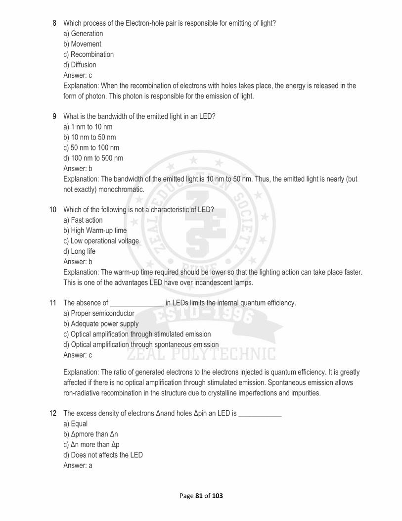
Page 81 of 103
8 Which process of the Electron-hole pair is responsible for emitting of light?
a) Generation
b) Movement
c) Recombination
d) Diffusion
Answer: c
Explanation: When the recombination of electrons with holes takes place, the energy is released in the
form of photon. This photon is responsible for the emission of light.
9 What is the bandwidth of the emitted light in an LED?
a) 1 nm to 10 nm
b) 10 nm to 50 nm
c) 50 nm to 100 nm
d) 100 nm to 500 nm
Answer: b
Explanation: The bandwidth of the emitted light is 10 nm to 50 nm. Thus, the emitted light is nearly (but
not exactly) monochromatic.
10 Which of the following is not a characteristic of LED?
a) Fast action
b) High Warm-up time
c) Low operational voltage
d) Long life
Answer: b
Explanation: The warm-up time required should be lower so that the lighting action can take place faster.
This is one of the advantages LED have over incandescent lamps.
11 The absence of _______________ in LEDs limits the internal quantum efficiency.
a) Proper semiconductor
b) Adequate power supply
c) Optical amplification through stimulated emission
d) Optical amplification through spontaneous emission
Answer: c
Explanation: The ratio of generated electrons to the electrons injected is quantum efficiency. It is greatly
affected if there is no optical amplification through stimulated emission. Spontaneous emission allows
ron-radiative recombination in the structure due to crystalline imperfections and impurities.
12 The excess density of electrons Δnand holes Δpin an LED is ____________
a) Equal
b) Δpmore than Δn
c) Δn more than Δp
d) Does not affects the LED
Answer: a
Page 82 of 103
Explanation: The excess density of electrons ΔnandΔp (holes) is equal. The charge neutrality is
maintained within the structure due to injected carriers that are created and recombined in pairs. The
power generated internally by an LED is determined by taking into considering the excess electrons and
holes in p- and n-type material respectively.
13 The hole concentration in extrinsic materials is _________ electron concentration.
a) much greater than
b) lesser than
c) equal to
d) negligible difference with
Answer: a
Explanation: In extrinsic materials, one carrier type will be highly concentrated than the other type. Hence
in p-type region, hole concentration is greater than electron concentration in context of extrinsic material.
This excess minority carrier density decays with time.
14 The carrier recombination lifetime becomes majority or injected carrier lifetime.
a) True
b) False
Answer: b
Explanation: The initial injected excess electron density and ηrepresents the total carrier recombination
time. In most cases, Δnis a small fraction of majority carriers and contains all minority carriers. So in
these cases, carrier recombination lifetime becomes minority injected carrier lifetime ηi.
15 In a junction diode, an equilibrium condition occurs when ____________
a) Δngreater than Δp
b) Δnsmaller than Δp
c) Constant current flow
d) Optical amplification through stimulated emission
Answer: c
Explanation: The total rate at which carriers are generated in sum of externally supplied and thermal
generation rates. When there is a constant current flow in this case, an equilibrium occurs in junction
diode.
16
Determine the total carrier recombination lifetime of a double heterojunction LED where the radioactive
and nonradioactive recombination lifetime of minority carriers in active region are 70 ns and 100 ns
respectively.
a) 41.17 ns
b) 35 ns
c) 40 ns
d) 37.5 ns
Answer: a
Explanation: The total carrier recombination lifetime is given by
η = ηrηnr/ηr+ηnr = 70× 100/70 + 100 ns = 41.17 ns
Where
Page 83 of 103
ηr = radiative recombination lifetime of minority carriers
ηnr = nonradioactive recombination lifetime of minority carriers.
17
Determine the internal quantum efficiency generated within a device when it has a radiative
recombination lifetime of 80 ns and total carrier recombination lifetime of 40 ns.
a) 20 %
b) 80 %
c) 30 %
d) 40 %
Answer: b
Explanation: The internal quantum efficiency of device is given by
ηint = η/ηr = 40/80 ×100 = 80%
Where
η = total carrier recombination lifetime
ηr = radiative recombination lifetime.
18
Compute power internally generated within a double-heterojunction LED if it has internal quantum
efficiency of 64.5 % and drive current of 40 mA with a peak emission wavelength of 0.82 μm.
a) 0.09
b) 0.039
c) 0.04
d) 0.06
Answer: b
Explanation: The power internally generated within device i.e. double-heterojunction LED can be
computed by
Pint = ηint hci/eλ = 0.645×6.626×10-34×3×108×40×10-3/ 1.602×10-19 × 0.82 × 10-6
= 0.039 W
Where
ηint = internal quantum efficiency
h = Planck’s constant
c = velocity of light
i = drive current
e = electron charge
λ = wavelength.
19 The Lambertian intensity distribution __________ the external power efficiency by some percent.
a) Reduces
b) Does not affects
c) Increases
d) Have a negligible effect
Answer: a
Page 84 of 103
Explanation: In Lambertian intensity distribution, the maximum intensity I0is perpendicular to the planar
surface but is reduced on the
sides in proportion to the cosine of θ i.e. viewing angle as apparent area varies with this angle. This
reduces the external power
efficiency. This is because most of the light is tapped by total internal refraction when radiated at greater
than the critical angle
for crystal air interface.
20
A planar LED fabricated from GaAs has a refractive index of 2.5. Compute the optical power emitted
when transmission factor is 0.68.
a) 3.4 %
b) 1.23 %
c) 2.72 %
d) 3.62 %
Answer: c
Explanation: The optical power emitted is given by
Pe = PintFn2/4nx2 = Pint (0.680×1/4×(2.5)2) = 0.0272 Pint.
Hence power emitted is only 2.72 % of optional power emitted internally.
Where,
Fn2 = transmission factor
nx = refractive index.
21
A planar LED is fabricated from GaAs is having a optical power emitted is 0.018% of optical power
generated internally which is 0.018% of optical power generated internally which is 0.6 P. Determine
external power efficiency.
a) 0.18%
b) 0.32%
c) 0.65%
d) 0.9%
Answer: d
Explanation: Optical power generated externally is given by
ηcp = (0.018Pint/2Pint)*100
Where,
Pint = power emitted
ηcp = external power efficiency.
22 For a GaAs LED, the coupling efficiency is 0.05. Compute the optical loss in decibels.
a) 12.3 dB
b) 14 dB
c) 13.01 dB
d) 14.6 dB
Answer: c
Explanation: The optical loss in decibels is given by-
Loss = -10log10 ηc
Where,
Page 85 of 103
ηc = coupling efficiency.
23
In a GaAs LED, compute the loss relative to internally generated optical power in the fiber when there is
small air gap between LED
and fiber core. (Fiber coupled = 5.5 * 10-4Pint)
a) 34 dB
b) 32.59 dB
c) 42 dB
d) 33.1 dB
Answer: b
Explanation: The loss in decibels relative to Pint is given by-
Loss = -10log10Pc/Pint
Where,
Pc = 5.5 * 10-4Pint.
24
Determine coupling efficiency into the fiber when GaAs LED is in close proximity to fiber core having
numerical aperture of 0.3.
a) 0.9
b) 0.3
c) 0.6
d) 0.12
Answer: a
Explanation: The coupling efficiency is given by
ηc = (NA)2 = (0.3)2 = 0.9.
25
If a particular optical power is coupled from an incoherent LED into a low-NA fiber, the device must
exhibit very high radiance.
a) True
b) False
Answer: a
Explanation: Device must have very high radiance specially in graded index fiber where Lambertian
coupling efficiency with same NA is about half that of step-index fibers. This high radiance is obtained
when direct band gap semiconductors are fabricated with DH structure driven at high current densities
26 The amount of radiance in planer type of LED structures is ____________
a) Low
b) High
c) Zero
d) Negligible
Answer: a
Explanation: Planer LEDs are fabricated using liquid or vapor phase epitaxial processes. Here p-type is
diffused into n-type substrate which creates junction. Forward current flow through junction provides
Lambertian spontaneous emission. Thus, device emits light from all surfaces. However a limited amount
of light escapes the structure due to total internal reflection thus providing low radiance.
Page 86 of 103
27 In optical fiber communication _____________ major types of LED structures are used.
a) 2
b) 4
c) 6
d) 3
Answer: c
Explanation: Optical fiber communication involves the use of 6 different major LED structure. These are
the surface emitter, edge emitter, the super luminescent, the resonant cavity LED, planar LEDs and
Dome LEDs
28
As compared to planar LED structure, Dome LEDs have ______________ External power efficiency
___________ effective emission area and _____________ radiance.
a) Greater, lesser, reduced
b) Higher, greater, reduced
c) Higher, lesser, increased
d) Greater, greater, increased
Answer: b
Explanation: In Dome LEDs, the diameter of dome is selected so as to maximum the internal emission
reaching surface within critical angle of GaAs. Thus, dome LEDs have high external power efficiency.
The geometry of Dome LEDs is such that dome is much larger than active recombination area, so it has
greater emission era and reduced of radiance.
29
The techniques by Burros and Dawson in reference to homo structure device is to use an etched well in
GaAs structure.
a) True
b) False
Answer: a
Explanation: Burros and Dawson provided a technique to restrict emission to small active region within
device thus providing high radiance. Etched well in a GaAs substrate is used to prevent heavy absorption
of emitted region and physically accommodating the fiber. These structures provide low thermal
impedance allowing high current densities of high radiance.
30 In surface emitter LEDs, more advantage can be obtained by using ____________
a) BH structures
b) QC structures
c) DH structures
d) Gain-guided structure
Answer: c
Explanation: DH structures provide high efficiency from electrical and optical confinement. Along with
efficiency, they provide less absorption of emitted radiation.
Page 87 of 103
31 Internal absorption in DH surface emitter Burros type LEDs is ____________
a) Cannot be determined
b) Negligible
c) High
d) Very low
Answer: d
Explanation: The larger band gap confining layers and the reflection coefficient at the back crystal space
is high in DH surface emitter Burros type LEDs. This provides good forward radiance. Thus these
structure LEDs have very less internal absorption.
32 DH surface emitter generally give ____________
a) More coupled optical power
b) Less coupled optical power
c) Low current densities
d) Low radiance emission into-fiber
Answer: a
Explanation: The optical power coupled into a fiber depends on distance, alignment between emission
area and fiber, SLED emission pattern and medium between emitting area and fiber. All these
parameters if considered, reduces refractive index mismatch and increases external power efficiency
thus providing more coupled optical power.
33 A DH surface emitter LED has an emission area diameter of 60μm. Determine emission area of source.
a) 1.534*10-6
b) 5.423*10-3
c) 3.564*10-2
d) 2.826*10-9
Answer: d
Explanation: The emission area A of source is given by
A = π(30*10-6) 2= 2.826*10-9cm2.
34
Estimate optical power coupled into fiber of DH SLED having emission area of 1.96*10-5, radiance of 40
W/rcm2, numerical aperture of 0.2 and Fresnel reflection coefficient of 0.03 at index matched fiber
surface.
a) 5.459*10-5
b) 1.784*10-3
c) 3.478*102
d) 9.551*10-5
Answer: d
Explanation: The optical power coupler in the step index fiber of SLED is given by
Pc = π(1-r) A RD(NA) 2
= 3.14 (1-0.03)*1.96*10-5*40*(0.2) 2
= 9.551*10-5W.
Page 88 of 103
35 In a multimode fiber, much of light coupled in the fiber from an LED is ____________
a) Increased
b) Reduced
c) Lost
d) Unaffected
Answer: c
Explanation: Optical power from an incoherent source is initially coupled into large angle rays falling
within acceptance angle of fiber but have more energy than Meridional rays. Energy from these rays
goes into the cladding and thus may be lost.
36
Determine the overall power conversion efficiency of lens coupled SLED having forward current of 20 mA
and forward voltage of 2 V with 170 μWof optical power launched into multimode step index fiber.
a) 1.256*10-5
b) 4.417*102
c) 4.25*10-3
d) 2.14*10-3
Answer: c
Explanation: The overall power conversion efficiency is determined by
η pc = Pc/P = 170*10-6/20*10-3*2
37
The overall power conversion efficiency of electrical lens coupled LED is 0.8% and power applied 0.0375
V. Determine optical power launched into fiber.
a) 0.03
b) 0.05
c) 0.3
d) 0.01
Answer: a
Explanation: Optical power launched can be computed by
η pc = Pc/P
Pc = η pc* P
= 0.03.
38 Mesa structured SLEDs are used ____________
a) To reduce radiance
b) To increase radiance
c) To reduce current spreading
d) To increase current spreading
Answer: c
Explanation: The planar structures of Burros-type LED allow lateral current spreading specially for
contact diameters less than 25 μm.This results in reduced current density and effective emission area
greater than contact area. This technique to reduce current spreading in very small devices is Mesa
structured SLEDs.
Page 89 of 103
39 The InGaAsP is emitting LEDs are realized in terms of restricted are ____________
a) Length strip geometry
b) Radiance
c) Current spreading
d) Coupled optical power
Answer: a
Explanation: The short striped structure of these LEDs around 100 μmimproves the external efficiency of
LEDs by reducing internal absorption of carriers. These are also called truncated strip E-LEDs.
40 The active layer of E-LED is heavily doped with ____________
a) Zn
b) Eu
c) Cu
d) Sn
Answer: a
Explanation: Zn doping reduces the minority carrier lifetime. Thus this improves the device modulation
bandwidth hence active layer is doped in Zn in E-LEDs.
41 A dipole antenna is also called as?
a) Marconi antenna
b) Yagi antenna
c) Bidirectional antenna
d) Hertz antenna
Answer: d
Explanation: One of the most widely used antenna types is the half-wave dipole antenna. This antenna is
also formally known as the Hertz antenna after Heinrich Hertz, who first demonstrated the existence of
electromagnetic waves.
42 The impedance at the center of the antenna is known as?
a) Characteristic impedance
b) Radiation resistance
c) Transmission impedance
d) Recovery resistance
Answer: b
Explanation: The transmission line is connected at the center. The dipole has an impedance of 73 V at its
center, which is the radiation resistance. At the resonant frequency, the antenna appears to be a pure
resistance of 73 V
Page 90 of 103
43
What happens when the radiation resistance of the antenna matches the characteristic impedance of the
transmission line?
a) No transmission occurs
b) No reception occurs
c) SWR is maximum
d) SWR is minimum
Answer: d
Explanation: When the radiation resistance of the antenna matches the characteristic impedance of
the transmission line, the SWR is minimum and maximum power reaches the antenna. This allows
maximum power to be transmitted.
44 The type of dipole antenna that has a higher band width is called as?
a) Conical antenna
b) Yagi antenna
c) Helical antenna
d) Marconi antenna
Answer: a
Explanation: A common way to increase bandwidth in the antenna is to use a version of the dipole
antenna known as the conical antenna. The overall length of the antenna is 0.73λ or 0.73(984)/f =
718.32/f. This is longer than the traditional one-half wavelength of a dipole antenna, but the physical
shape changes the necessary dimensions for resonance.
45 The radiation pattern of a half-wave dipole has the shape of a ______
a) Doughnut
b) Sphere
c) Hemisphere
d) Circular
Answer: a
Explanation: The radiation pattern of any antenna is the shape of the electromagnetic energy radiated
from or received by that antenna. Typically that radiation is concentrated in a pattern that has a
recognizable geometric shape. The radiation pattern of a half-wave dipole has the shape of a doughnut.
46 What is the beam width for a half wave dipole antenna?
a) 90°
b) 180°
c) 50°
d) 250°
Answer: a
Explanation: The beam width is measured between the points on the radiation curve that are 3 dB down
from the maximum amplitude of the curve. The maximum amplitude of the pattern occurs at 0° and 180°.
The 3-dB down points are 70.7 percent of the maximum. The angle formed with two lines extending from
the center of the curve to these 3-dB points is the beam width. The beam width is 90°. The smaller the
beam width angle, the more directional the antenna.
Page 91 of 103
47 What does the beam width of an antenna tell us?
a) Signal strength
b) Signal power
c) Directivity
d) Degradation
Answer: c
Explanation: The measure of an antenna’s directivity is beam width, the angle of the radiation pattern
over which a transmitter’s energy is directed or received. Beam width is measured on an antenna’s
radiation pattern.
48 What is the power radiated by the antenna with gain called as?
a) Critical power
b) Transverse power
c) Effective radiated power
d) Transmitted power
Answer: c
Explanation: The power radiated by an antenna with directivity and therefore gain is called the effective
radiated power (ERP). The ERP is calculated by multiplying the transmitter power fed to the antenna Pt
by the power gain Ap of the antenna.
49 What is the radiation pattern of an isotropic radiator?
a) Doughnut
b) Sphere
c) Hemisphere
d) Circular
Answer: b
Explanation: An isotropic radiator is a theoretical point source of electromagnetic energy. The E and H
fields radiate out in all directions from the point source, and at any given distance from the point source,
the fields form a sphere.
50 What is the impedance of the folded dipole antenna?
a) 50Ω
b) 100Ω
c) 300Ω
d) 20Ω
Answer: c
Explanation: A popular variation of the half-wave dipole is the folded dipole. Like the standard dipole, it is
one-half wavelength long. However, it consists of two parallel conductors connected at the ends with one
side open at the center for connection to the transmission line. The impedance of this popular antenna is
300 V, making it an excellent match for the widely available 300-V twin lead.
Page 92 of 103
51 Which of the following antennas produce a vertical radiation pattern?
a) Dipole antenna
b) Yagi antenna
c) Marconi antenna
d) Hertz antenna
Answer: c
Explanation: The same effect as dipole antenna can be achieved with a one-quarter wavelength antenna
or Marconi antenna. A vertical dipole with the doughnut-shaped radiation pattern, in which one-half of the
pattern is below the surface of the earth. This is called a vertical radiation pattern.
52
The members of the antenna family which are made of wires of certain value in terms of operating
wavelength are called:
a) Loop antennas
b) Wire antennas
c) Dipole antenna
d) Slot antennas
Answer: c
Explanation: Wires of half wavelength are termed as dipoles. Their radiation resistance is about 73 Ω. If
only half of this length is used, then it is called quarter-wave monopole with a radiation resistance of 36.5
Ω.
53 The antenna in which location of the feed determines the direction of the lobe are:
a) Wire antenna
b) Loop antenna
c) Helical antenna
d) Horn antenna
Answer: a
Explanation: In a wire antenna, the location of the feed determines the direction of the lobe and the
orientation of the wire determines the polarization. These wires can be thick or thin. Thickness of the wire
determines the radiation resistance of the antenna.
54
Based on the size of the loops, loop antennas are classified as small and large loops. This is the only
classification of loop antenna.
a) True
b) False
Answer: b
Explanation: Loop antennas are classified based on various antenna parameters. To name a few, small
and large loops, circular and square loops, loops having single or multi turns, loops with turns wound
using a single wire or multiple wires.
Page 93 of 103
55 Antenna that does not belong to the horn antenna family among the following are:
a) Pyramidal horn
b) Conical horn
c) bi-conical horn
d) None of the mentioned
Answer: d
Explanation: All of the above mentioned antennas belong to the horn antenna family. Horn antennas may
be made of pointed or rounded waveguides. The waveguides may contain disc at an end or some
dielectric.
56 Patch antennas are the antennas of small size and are made of:
a) Strip line
b) Microstrip lines
c) Coaxial cables
d) Rectangular waveguide
Answer: b
Explanation: Patch antennas are microstrip antennas that can be of any shape. Patch antennas can be
aperture-coupled fed or proximity fed. For obtaining circular polarization, a patch may also be doubly fed.
57 Reflector antennas are widely used to modify radiation patterns of radiating elements.
a) True
b) False
Answer: a
Explanation: Reflector antennas are used to modify radiation patterns of radiating elements. Reflector
antennas are classified into two categories. They are passive reflectors and active reflectors. Based on
the type of the radiating element and the modification in the radiation pattern required, accordingly either
active or passive reflectors are chosen.
58 The pattern of the reflector in a reflector antenna is called:
a) Primary pattern
b) Secondary pattern
c) Reflector pattern
d) None of the mentioned
Answer: b
Explanation: In a reflector antenna, the feed pattern is called primary pattern and the pattern of the
reflector is called secondary pattern. These antennas are widely employed in RADARs and other types of
point to point communication links.
Page 94 of 103
59 ______ antennas have gain less than reflector antennas but have more lenient tolerance on surfaces.
a) Helical antennas
b) Lens antennas
c) Array antennas
d) Slot antennas
Answer: b
Explanation: Lens antennas are complex in nature but are able to scale wider angles. In comparison to
reflectors, their gain is 1 or 2 dB less, but these have more lenient tolerance on surfaces. These have
less rearward reflection, relatively low loss and can be easily shaped to the desired contours.
60 Lens antennas are classified into two types. One being fast antenna, the other one is:
a) Slow antenna
b) Delay antenna
c) Dynamic antenna
d) None of the mentioned
Answer: b
Explanation: In delay lenses, the electrical path length is increased or the wave is retarded by the lens
medium. Dielectric lenses and H-plane metal lenses fall in this category.
61
The antennas which offer high operational bandwidth and the antenna parameters are maintained over a
wide range of antennas are called:
a) Wide band antennas
b) Array antennas
c) Parabolic antennas
d) None of the mentioned
Answer: a
Explanation: In this class of antennas, constancy of impedance and radiation characteristics is
maintained over a wide range of frequencies. To be wide band or frequency independent, antennas
should expand or contract in proportion to the wavelength.
62 High directivity required in RADAR communication is satisfied using this type of antennas:
a) Wide band antennas
b) Antenna arrays
c) Slot antennas
d) Patch antennas
Answer: b
Explanation: Higher directivity is the requirement in point to point communication. This can be achieved
by increasing the size of the antennas in terms of electrical length. When much high directivity is
required, antenna arrays are used.
Page 95 of 103
63
The terminal impedance of a dipole antenna is 710 Ω. The terminal impedance of the slot antenna given
the intrinsic impedance of air is 377 Ω is:
a) 100 Ω
b) 50 Ω
c) 25 Ω
d) None of the mentioned
Answer: b
Explanation: The terminal impedance ZS of the slot is given by the relation Z02/ 4Zd) Zₒ is the intrinsic
impedance of the medium and ZD is the terminal impedance of the dipole. Substituting the given values
in the above equation, the terminal impedance of sot is 50 Ω.
64
If the length of aperture in a pyramidal horn antenna is 10cm and δ for the design is 0.25. Then, the
flaring angle of the pyramidal horn is:
a) 30⁰
b) 25.4⁰
c) 45⁰
d) 60⁰
Answer: b
Explanation: The flaring angle of pyramidal horn is given by 2cos-1(L/L+δ). Substituting the values of L
and δ, flaring angle is 25.4⁰ .
65
If the directivity of a square corner receiving antenna is 20 and operating at a wavelength of 0.25m, the
effective aperture of a square corner antenna is:
a) 0.4 m2
b) 0.2 m2
c) 0.1 m2
d) None of the mentioned
Answer: a
Explanation: Given the directivity of the antenna, effective aperture of the antenna is given by Dλ2/4π.
substituting the given values of the variables; the effective aperture of the antenna is 0.4 m2.
66 Micro strip can be fabricated using:
a) Photo lithographic process
b) Electrochemical process
c) Mechanical methods
d) None of the mentioned
Answer: a
Explanation: Microstrip lines are planar transmission lines primarily because it can be fabricated by
photolithographic processes and is easily miniaturized and integrated with both passive and active
microwave devices.
Page 96 of 103
67 The mode of propagation in a microstrip line is:
a) Quasi TEM mode
b) TEM mode
c) TM mode
d) TE mode
Answer: a
Explanation: The exact fields of a microstrip line constitute a hybrid TM-TE wave. In most practical
applications, the dielectric substrate is very thin and so the fields are generally quasi-TEM in nature.
68 Microstrip line can support a pure TEM wave.
a) True
b) False
c) Microstrip supports only TM mode
d) Microstrip supports only TE mode
Answer: b
Explanation: The modeling of electric and magnetic fields of a microstrip line constitute a hybrid TM-TE
model. Because of the presence of the very thin dielectric substrate, fields are quasi-TEM in nature. They
do not support a pure TEM wave.
69 The effective di electric constant of a microstrip line is:
a) Equal to one
b) Equal to the permittivity of the material
c) Cannot be predicted
d) Lies between 1 and the relative permittivity of the micro strip line
Answer: d
Explanation: The effective dielectric constant of a microstrip line is given by (∈r + 1)/2 + (∈r-1)/2 * 1/
(√1+12d/w). Along with the relative permittivity, the effective permittivity also depends on the effective
width and thickness of the microstrip line.
70 Effective dielectric constant of a microstrip is given by:
a) (∈r + 1)/2 + (∈r-1)/2 * 1/ (√1+12d/w)
b) (∈r+1)/2 + (∈r-1)/2
c) (∈r+1)/2 (1/√1+12d/w)
d) (∈r + 1)/2-(∈r-1)/2
Answer: a
Explanation: The effective dielectric constant of a microstrip line is (∈r + 1)/2 + (∈r-1)/2 * 1/ (√1+12d/w).
This relation clearly shows that the effective permittivity is a function of various parameters of a microstrip
line, the relative permittivity, effective width and the thickness of the substrate.
Page 97 of 103
71
The effective dielectric constant of a micro strip line is 2.4, then the phase velocity in the micro strip line
is given by:
a) 1.5*108 m/s
b) 1.936*108 m/s
c) 3*108 m/s
d) None of the mentioned
Answer: b
Explanation: The phase velocity in a microstrip line is given by C/√∈r. substituting the value of relative
permittivity and the speed of light in vacuum, the phase velocity is 1.936*108 m/s.
72
The effective di electric constant of a micro strip line with relative permittivity being equal to 2.6, with a
width of 5mm and thickness equal to 8mm is given by:
a) 2.6
b) 1.97
c) 1
d) 2.43
Answer: b
Explanation: The effective dielectric constant of a microstrip line is given by (∈r + 1)/2 + (∈r-1)/2 * 1/
(√1+12d/w). Substituting the given values of relative permittivity, effective width, and thickness, the
effective dielectric constant is 1.97.
73
If the wave number of an EM wave is 301/m in air , then the propagation constant β on a micro strip line
with effective di electric constant 2.8 is:
a) 602
b) 503.669
c) 150
d) 200
Answer: b
Explanation: The propagation constant β of a microstrip line is given by k0√∈e. ∈e is the effective
dielectric constant. Substituting the relevant values, the effective dielectric constant is 503.669.
74 For most of the micro strip substrates:
a) Conductor loss is more significant than di electric loss
b) Di electric loss is more significant than conductor loss
c) Conductor loss is not significant
d) Di-electric loss is less significant
Answer: a
Explanation: Surface resistivity of the conductor (microstrip line) contributes to the conductor loss of a
microstrip line. Hence, conductor loss is more significant in a microstrip line than dielectric loss.
Page 98 of 103
75 The wave number in air for EM wave propagating on a micro strip line operating at 10GHz is given by:
a) 200
b) 211
c) 312
d) 209
Answer: d
Explanation: The wave number in air is given by the relation 2πf/C. Substituting the given value of
frequency and ‘C’, the wave number obtained is 209.
76 The effective dielectric constant ∈r for a microstrip line:
a) Varies with frequency
b) Independent of frequency
c) It is a constant for a certain material
d) Depends on the material used to make microstrip
Answer: b
Explanation: The effective dielectric constant of a microstrip line is given by (∈r + 1)/2 + (∈r-1)/2 * 1/
(√1+12d/w). The equation clearly indicates that the effective dielectric constant is independent of the
frequency of operation, but depends only on the design parameters of a microstrip line.
77
With an increase in the operating frequency of a micro strip line, the effective di electric constant of a
micro strip line:
a) Increases
b) Decreases
c) Independent of frequency
d) Depends on the material of the substrate used as the microstrip line
Answer: c
Explanation: As the relation between effective permittivity and the other parameters of a microstrip line
indicate, effective dielectric constant is not a frequency dependent parameter and hence remains
constant irrespective of the operation of frequency.
78 All EM waves propagate at the speed of light irrespective of medium.
a) True
b) False
Answer: b
Explanation: The speed of light depends on the medium through which it travels and it the same for EM
waves as light can be thought of an EM wave. The speed of EM waves is maximum in a vacuum.
79
In a current carrying conductor, what happens to the magnetic field produced if the supplied voltage is
increased and current is maintained constant?
a) Field strength increases
b) Field radius increases
c) Filed strength decreases
d) Does not change
Page 99 of 103
Answer: d
Explanation: The magnetic field produced by a current carrying conductor is only influenced by the
current and not the voltage. Since the current is maintained constant, there is no change in the magnetic
field strength or radius.
80 Which of the following is the most necessary for an electric field to exist?
a) Current
b) Potential difference
c) Dielectric material
d) Metal conductor
Answer: b
Explanation: The most important thing for an electric field to exist is a potential difference between two
conductors. It is not that only metal conductors can produce an electric field, potential difference between
fluids also produces electric fields.
81
What happens to the electric field between two conductors when the permeability of the material between
the plates is increased?
a) Field strength increases
b) Field radius decreases
c) Field strength decreases
d) Nothing happens
Answer: d
Explanation: The permeability of a material only affects the magnetic field and not the electric field.
Electric field depends upon permittivity of the material between the two conductors.
82 Which of the following is not true?
a) A conductor carrying alternating current radiates
b) A transmission line must not radiate energy
c) Antennas are transmission lines which are made to radiate energy
d) A parallel wire transmission, when left open, does not radiate
Answer: d
Explanation: If a parallel-wire transmission line is left open, the electric and magnetic fields escape from
the end of the line and radiate into space. This radiation, however, is inefficient and unsuitable for reliable
transmission or reception.
83 The radiation from an open line can be increased by bending to which of the following angle?
a) 0°
b) 180°
c) 90°
d) 53.76°
Answer: c
Page 100 of 103
Explanation: The radiation from a transmission line can be greatly improved by bending the transmission
line conductors so that they are at a right angle to the transmission line. The magnetic fields no longer
cancel and, in fact, aid one another. The electric field spreads out from conductor to conductor. The
result is an antenna.
84 What is the ratio of the electric field strength of a radiated wave to the magnetic field strength called?
a) Impedance of space
b) Dielectric constant
c) Permittivity
d) Permeability
Answer: a
Explanation: The ratio of the electric field strength of a radiated wave to the magnetic field strength is a
constant. It is called the impedance of space, or the wave impedance.
85 The fields in the Fresnel zone are radio waves that contain the information transmitted.
a) True
b) False
Answer: b
Explanation: The near field describes the region directly around the antenna where the electric and
magnetic fields are distinct. These fields are not the radio wave, but they do indeed contain any
information transmitted. The near field is also referred to as the Fresnel zone.
86 At what distance from the antenna does the far field start?
a) 2 wavelengths
b) 5 wavelengths
c) 10 wavelengths
d) 25 wavelengths
Answer: c
Explanation: The far field that is approximately 10 wavelengths from the antenna is the radio wave with
the composite electric and magnetic fields. For example, at 2.4 GHz, one wavelength is 984/2400 = 0.41
feet. The far field is 10 times that, or 4.1 ft or beyond.
87 The Far field is also known as ______________
a) Fresnel zone
b) Fraunhofer zone
c) Maxwell zone
d) Marconi zone
Answer: b
Explanation: The far field is also called the Fraunhofer zone. It is named after the Bavarian physicist
Joseph Ritter von Fraunhofer.

Page 101 of 103
88
An Em wave is said to be vertically polarized when the angle between the electrical field and earth is
_______
a) 50°
b) 20°
c) 90°
d) 180°
Answer: c
Explanation: Polarization refers to the orientation of magnetic and electric fields with respect to the earth.
If an electric field is parallel to the earth, the electromagnetic wave is said to be horizontally polarized; if
the electric field is perpendicular to the earth, the wave is vertically polarized.
89 Which of the following is not true?
a) Right circular polarized antennas can pick up left circular polarized waves due to propagation effects
b) Circular polarization has lesser attenuation in free space
c) Circular polarized wave can follow the curvature of earth
d) In circular polarization the electric and magnetic fields rotate as they leave the antenna
Answer: c
Explanation: In circular polarized wave the polarization angle of the electric field and the earth is
continuously changing. This does not affect the transmission direction and hence circular polarized
waves cannot bend with the curvature of earth, like any other EM wave.
90 What happens when a vertical or horizontal polarized antenna receives a circular polarized wave?
a) Gain increases
b) Signal strength increases
c) Signal strength reduces
d) Cannot receive circular polarized waves
Answer: c
Explanation: A vertical or horizontal antenna can receive circular polarized signals, but the signal
strength is reduced. When circular polarization is used at both transmitter and receiver, both must use
either left- or right-hand polarization if the signal is to be received.
91 Which of the following devices assist in using the same antenna for transmission and receiving?
a) Monoplexer
b) Multiplexer
c) Duplexer
d) Switch
Answer: c
Explanation: An antenna can transmit and receive at the same time as long as some means is provided
for keeping the transmitter energy out of the front end of the receiver. A device called a duplexer is used
for this purpose.
Page 102 of 103
92 Crater wear occurs mainly on the
a) nose part, front relief face and side relief face of the cutting tool
b) face of the cutting tool at a short distance from the cutting edge only
c) cutting edge only
d) front face only
93 Flank wear depends upon the
a) hardness of the work and tool material at the operating temperature
b) amount and distribution of hard constituents in the work material
c) degree of strain hardening in the chip
d) none of the mentioned
Answer: b
Explanation: Flank wear occurs as a result of friction between the progressively increasing contact area
on the tool flank.
94 Crater wear is predominant in
a) carbon steels
b) tungsten carbide tools
c) high speed steel tools
d) ceramic tools
Answer: b
Explanation: Crater wear is usually found while machining brittle materials and tungsten carbide tools
favour this phenomenon.
95 Flank wear is due to the abrasive action of hard mis-constituents.
a) True
b) False
Answer: a
Explanation: Flank wear is due to the abrasive action of hard mis-constituents including debris from built
up edge as the work material rubs the work surface.
96 Crater wear is mainly due to the phenomenon is known as
a) adhesion of metals
b) oxidation of metals
c) diffusion of metals
d) none of the mentioned
Answer: c
Explanation: Flank wear is due to the abrasive action and crater wear is due to diffusion of metals.
Page 103 of 103
97 Crater wear leads to
a) increase in cutting temperature
b) weakening of tool
c) friction and cutting forces
d) all of the mentioned
Answer: d
98 The tool may fail due to
a) cracking at the cutting edge due to thermal stresses
b) chipping of the cutting edge
c) plastic deformation of the cutting edge
d) all of the mentioned
Answer: d
99 Flank wear occurs mainly on the
a) nose part, front relief face and side relief face of the cutting tool
b) face of the cutting tool at a short distance from the cutting edge only
c) cutting edge only
d) front face only
Answer: a
Explanation: Crater wear occurs on the rake face of the tool, while flank wear occurs on the relief (flank)
face of
the tool.
100 Tool life is measured by the
a) number of pieces machined between tool sharpenings
b) time the tool is in contact with the job
c) volume of material removed between tool sharpenings
d) all of the mentioned
Answer: d
Prepared By
Badadhe P S
Verified By
Jadhav D G
Module Coordinator
Re-Verified By
Navale S N
Academic Coordinator
Approved By
Tupe S G
HoD E&Tc