proton radiation effects on nanocrystal non-volatile memories
TRANSCRIPT
IEEE TRANSACTIONS ON NUCLEAR SCIENCE, VOL. 54, NO. 4, AUGUST 2007 975
Proton Radiation Effects on NanocrystalNon-Volatile Memories
E. Verrelli, D. Tsoukalas, M. Kokkoris, R. Vlastou, P. Dimitrakis, Member, IEEE, and P. Normand
Abstract—We report on proton radiation effects onSi-nanocrystal (Si-NCs) MOS capacitors and nMOS transistorsaiming at non-volatile memory applications. Irradiationexperiments were conducted on NC MOS capacitors usingprotons of 1.5 MeV and 6.5 MeV and on NC nMOS transistorsusing protons of 1.5 MeV. The range of doses investigated was1 to 100Mrad(SiO2). A 2-D layer of Si NCs with 3 nm
mean diameter and 1012 cm 2 surface density was successfullyachieved by low-energy (1 keV) ion-beam-synthesis in thin SiO2
layers. After irradiation, programmed capacitors are found toundergo bit flip while programmed transistors are not. Chargeretention measurements at room temperature for the write anderase states of irradiated and non-irradiated samples reveal that asignificant memory window exists at an extrapolated time of tenyears even after an irradiation dose as high as 120 Mrad (SiO2).The flat-band decay rate of the erase state in NC MOS capacitorsdoes not depend on the irradiation-dose while the opposite occursfor the write state which is found to be directly dependent onvalues after irradiation. These results clearly indicate that NCNon-Volatile Memories (NVM) are promising radiation tolerantdevices.
Index Terms—Data retention, nanocrystal memories, non-volatile memory (NVM), proton radiation effects.
I. INTRODUCTION
RADIATION environments are encountered in military ap-plications, nuclear power stations, nuclear waste disposal
sites, high-altitude avionics, medical and space applications.Radiation type, energy, dose rate and total dose may be verydifferent in each of these application areas and require inmany cases radiation-tolerant electronic systems [1]. The wayradiation damages electronic systems depend strongly on theenvironment and can be classified as total ionizing dose effects(TID) and single event effects (SEE) [2], [3]. Of particularinterest are the radiation effects on non-volatile memory de-vices (NVM). While a major issue relates to the radiationsensitivity of the NVM control circuitry [4], [5], radiationalso affects the performance of the memory cells. At present,the dominant technology for NVM is based on the floatinggate (FG) concept. The most recent and dominant version of
Manuscript received October 6, 2006; revised May 2, 2007. This work wassupported by the program PROTAGORAS.
E. Verrelli, D. Tsoukalas, M. Kokkoris, and R. Vlastou are with the NationalTechnical University of Athens, GR-15773 Athens, Greece (e-mail: [email protected], [email protected], [email protected], [email protected]).
P. Dimitrakis and P. Normand are with the Institute of Microelectronics,NCSR “Demokritos,” 15310 Aghia Paraskevi, Greece (e-mail: [email protected], [email protected]).
Color versions of one or more of the figures in this paper are available onlineat http://ieeexplore.ieee.org.
Digital Object Identifier 10.1109/TNS.2007.902365
FG-NVM is the Flash EEPROM. Its tolerance to radiationhas been studied extensively by researchers in the past towardTID effects [4] and SEE effects [4], [5] and most recently byCellere et al. [6]–[8]. In order to overcome the technologicalconstraints imposed as the device size approaches dimensionsbelow 100 nm various memory alternatives are extensivelyinvestigated. A promising route for low-cost ultra-dense datastorage lies in the use of modified Flash structures such asnanocrystal memories (NC-NVM) [9]. Compared to standardFG-NVMs, NC-NVMs are expected to show higher toleranceto both TID and SEE effects because of the discrete nature ofthe charge storage centers. There are a few studies on radiationtolerance of NC-NVMs: Petkov [10] and Oldham [11] per-formed investigations toward this end. Petkov and coauthorsexplored TID effects using a source up to 15 Mrad(Si)while Oldham and coauthors used various heavy ions for SEEeffects and for TID effects up to 200 krad. In this workTID effects on NC-NVMs were investigated using protons of1.5 MeV and 6.5 MeV at doses up to 120 Mrad .
II. EXPERIMENTAL DETAILS
The devices under study were Si-NC MOS capacitors andSi-NC nMOS transistors fabricated using a 2 technology.The NCs were obtained by the ultra-low-energy ion-beam-syn-thesis technique, ULE-IBS [12]. Si-NC MOS capacitors werefabricated by implanting 1 keV silicon ions to a dose of2 into a 9 nm-thick layer thermally grown on ap-type Si substrate and subsequent furnace annealing at 950for 30 min in nitrogen diluted oxygen (1.5% per volume).The above process conditions lead to the formation of a 2-Dlayer of Si NCs with a mean diameter of about 2–3 nm anda surface density of . Subsequently, a 10 nm thickTEOS oxide was deposited on top of the structures and thermalannealing at 900 for 15 min in was followed. Then, NCMOS capacitors were defined by Al evaporation, lithographyand metal etching. TEM studies (not shown here) revealed thatthe final thickness of the NC- structures was 25.5 nm con-sisting of 8-nm thick injection oxide ( thickness betweenthe bottom of the NC-layer and the Si/ interface), 2 nm SiNC layer and 15.5 nm control oxide. Reference samples werealso prepared following the same process, excluding the siliconimplantation step. Si-NC nMOS transistors were fabricatedusing a 7 nm thick layer that was Si implanted andannealed under the same conditions as for NC MOS capacitors.No additional control oxide was deposited. Further details onthe transistor fabrication can be found elsewhere [12]. Thefinal gate dielectric stack includes 6.5 nm thick injection oxide,2.5 nm thick Si NC layer and 5 nm thick control oxide. The
0018-9499/$25.00 © 2007 IEEE
976 IEEE TRANSACTIONS ON NUCLEAR SCIENCE, VOL. 54, NO. 4, AUGUST 2007
TABLE IFLUENCIES AND DOSES FOR THE SAMPLES INVOLVED IN THIS EXPERIMENT
gate coupling factor [13], was found to be 0.66 and 0.43 forcapacitors and transistors respectively.
Devices were irradiated with 1.5 MeV and 6.5 MeV protonsusing a TANDEM accelerator equipped with a duoplasmatronsource for light ions and a sputter source for heavier ones, anaccelerator that can deliver high intensity beams (e.g., 40protons, 15 carbon). Fluencies were determined by inte-grating the measured proton current that was around 200 pA(70 krad ). Table I shows full details of irradiation ex-periments. The irradiated samples were measured within oneweek following irradiation time, while retention and endurancemeasurements were performed within one-month period. Irra-diations and electrical measurements were carried-out at roomtemperature.
III. RESULTS AND DISCUSSION
A. Capacitors
The density of interface states has beenevaluated using the high-low frequency method [14]. Accordingto this method, values through the Si energy band-gap areextracted by comparing the high-frequency (1 MHz) - withthe quasi-static one. Thus, the following equation can be usedto calculate
(1)
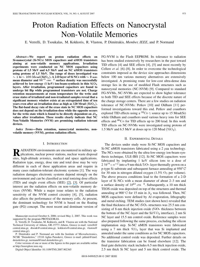
Fig. 1 shows the estimated at silicon midgap energy mea-sured on MOS capacitors as a function of proton irradiationdoses at different energies. For both reference and NC MOSdevices, increases sublinearly with dose. Within the mea-surement errors, our data are in good agreement with the rela-tionship that asserts to be proportional to [2].distributions (not shown here) in the Si energy band-gap werefound to be U shaped for the various MOS capacitor samples,
Fig. 1. D versus dose for Reference (without NCs) MOS and NC MOS ca-pacitors irradiated with protons 1.5 MeV and 6.5 MeV.D reference value fornon irradiated devices is also reported. The lines correspond to linear fits of theNC MOS capacitors experimental data to the relationshipD �Dose .
with a clear peak in the upper half of the band gap, at around0.2 eV above midgap, giving evidence of a sharply distributedelectron state.
The examined NC memory structures are written and erasedby electrons and holes, respectively. Charge injection takesplace from the Si substrate into the NCs by Fowler-Nordheim(FN) tunneling mechanism. The injection current densityin this case is described as a function of the oxide electric fieldby the following equation [15]:
(2)
VERRELLI et al.: PROTON RADIATION EFFECTS ON NANOCRYSTAL NON-VOLATILE MEMORIES 977
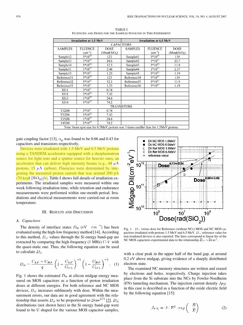
Fig. 2. B parameter of FN tunneling conduction measured on NC MOS capaci-tors for the 1.5 MeV and 6.5 MeV proton energies. B Reference values measuredon unirradiated samples are also shown. In the inset the same parameter mea-sured on irradiated Reference (without NCs) MOS capacitors.
where ,, and are the electron
rest and effective mass into the oxide, is the Si/ bar-rier height and E is the oxide electric field. The parameter Bof (2) is obtained from the slope of versusplot. In Fig. 2, the experimental values of B are reported as afunction of the irradiation dose. Within the experimental errorsand the statistical fluctuations observed from device to device(giving an overall estimated error of 10% of measured values),it can be concluded that the value of parameter B does not de-pend on the irradiation dose and remains unchanged before andafter irradiation. It should be noted that the values of parameterB for the reference devices (inset of Fig. 2) are higher than theones found on NC devices. This effect is attributed to the un-derlying physics governing the ULE-IBS technique where onlypart of the implanted Si ions contributes to the formation of NCsleaving a region in the oxide rich in Si atoms. As a consequence,energy states are created that lower the effective barrier of theoxide and consequently reduces B parameter values [16].
Samples irradiated with floating terminals exhibit - char-acteristics shifted to lower voltages compared to the characteris-tics of non-irradiated samples, in agreement to the well-knownobservation that irradiation creates a net trapped positive charge
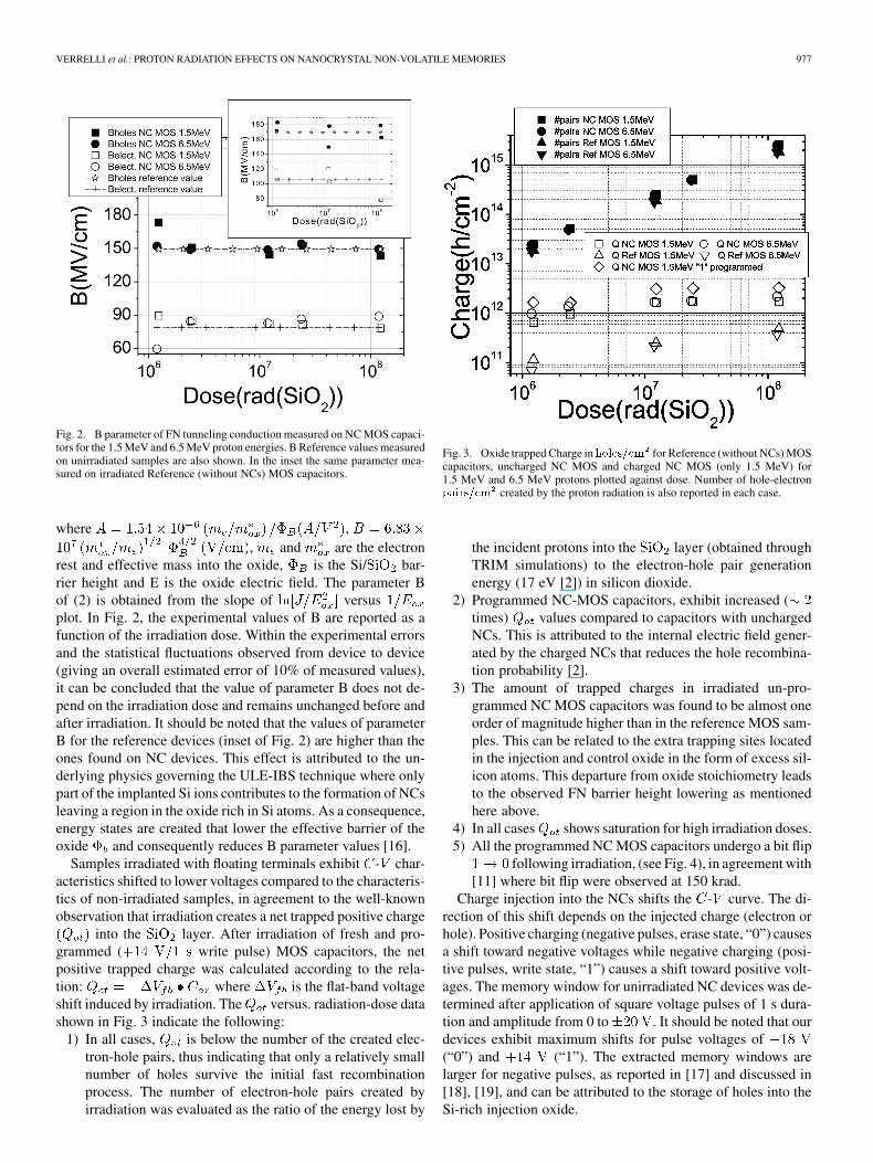
into the layer. After irradiation of fresh and pro-grammed ( write pulse) MOS capacitors, the netpositive trapped charge was calculated according to the rela-tion: where is the flat-band voltageshift induced by irradiation. The versus. radiation-dose datashown in Fig. 3 indicate the following:
1) In all cases, is below the number of the created elec-tron-hole pairs, thus indicating that only a relatively smallnumber of holes survive the initial fast recombinationprocess. The number of electron-hole pairs created byirradiation was evaluated as the ratio of the energy lost by
Fig. 3. Oxide trapped Charge in holes=cm for Reference (without NCs) MOScapacitors, uncharged NC MOS and charged NC MOS (only 1.5 MeV) for1.5 MeV and 6.5 MeV protons plotted against dose. Number of hole-electronpairs=cm created by the proton radiation is also reported in each case.
the incident protons into the layer (obtained throughTRIM simulations) to the electron-hole pair generationenergy (17 eV [2]) in silicon dioxide.
2) Programmed NC-MOS capacitors, exhibit increased (times) values compared to capacitors with unchargedNCs. This is attributed to the internal electric field gener-ated by the charged NCs that reduces the hole recombina-tion probability [2].
3) The amount of trapped charges in irradiated un-pro-grammed NC MOS capacitors was found to be almost oneorder of magnitude higher than in the reference MOS sam-ples. This can be related to the extra trapping sites locatedin the injection and control oxide in the form of excess sil-icon atoms. This departure from oxide stoichiometry leadsto the observed FN barrier height lowering as mentionedhere above.
4) In all cases shows saturation for high irradiation doses.5) All the programmed NC MOS capacitors undergo a bit flip
following irradiation, (see Fig. 4), in agreement with[11] where bit flip were observed at 150 krad.
Charge injection into the NCs shifts the - curve. The di-rection of this shift depends on the injected charge (electron orhole). Positive charging (negative pulses, erase state, “0”) causesa shift toward negative voltages while negative charging (posi-tive pulses, write state, “1”) causes a shift toward positive volt-ages. The memory window for unirradiated NC devices was de-termined after application of square voltage pulses of 1 s dura-tion and amplitude from 0 to . It should be noted that ourdevices exhibit maximum shifts for pulse voltages of(“0”) and (“1”). The extracted memory windows arelarger for negative pulses, as reported in [17] and discussed in[18], [19], and can be attributed to the storage of holes into theSi-rich injection oxide.
978 IEEE TRANSACTIONS ON NUCLEAR SCIENCE, VOL. 54, NO. 4, AUGUST 2007
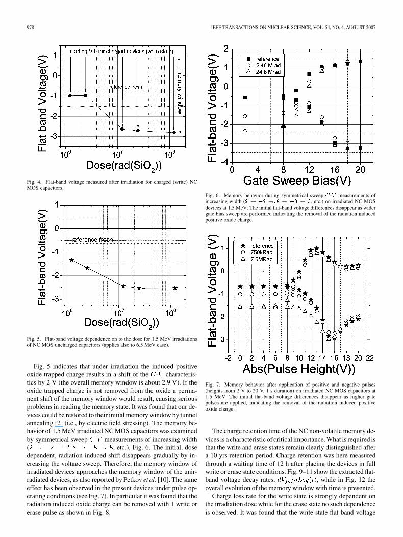
Fig. 4. Flat-band voltage measured after irradiation for charged (write) NCMOS capacitors.
Fig. 5. Flat-band voltage dependence on to the dose for 1.5 MeV irradiationsof NC MOS uncharged capacitors (applies also to 6.5 MeV case).
Fig. 5 indicates that under irradiation the induced positiveoxide trapped charge results in a shift of the - characteris-tics by 2 V (the overall memory window is about 2.9 V). If theoxide trapped charge is not removed from the oxide a perma-nent shift of the memory window would result, causing seriousproblems in reading the memory state. It was found that our de-vices could be restored to their initial memory window by tunnelannealing [2] (i.e., by electric field stressing). The memory be-havior of 1.5 MeV irradiated NC MOS capacitors was examinedby symmetrical sweep - measurements of increasing width( , etc.), Fig. 6. The initial, dosedependent, radiation induced shift disappears gradually by in-creasing the voltage sweep. Therefore, the memory window ofirradiated devices approaches the memory window of the unir-radiated devices, as also reported by Petkov et al. [10]. The sameeffect has been observed in the present devices under pulse op-erating conditions (see Fig. 7). In particular it was found that theradiation induced oxide charge can be removed with 1 write orerase pulse as shown in Fig. 8.
Fig. 6. Memory behavior during symmetrical sweep C-V measurements ofincreasing width (2 ! �2 !; 8 ! �8 ! 8, etc.) on irradiated NC MOSdevices at 1.5 MeV. The initial flat-band voltage differences disappear as widergate bias sweep are performed indicating the removal of the radiation inducedpositive oxide charge.
Fig. 7. Memory behavior after application of positive and negative pulses(heights from 2 V to 20 V, 1 s duration) on irradiated NC MOS capacitors at1.5 MeV. The initial flat-band voltage differences disappear as higher gatepulses are applied, indicating the removal of the radiation induced positiveoxide charge.
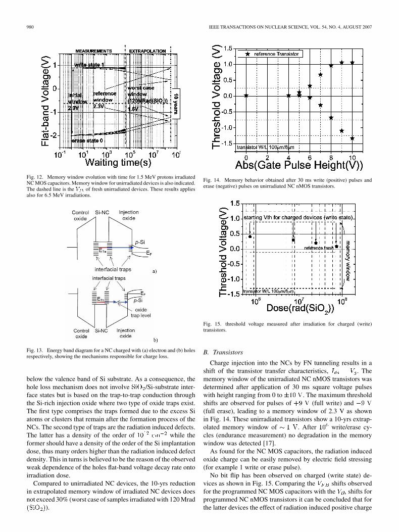
The charge retention time of the NC non-volatile memory de-vices is a characteristic of critical importance. What is required isthat the write and erase states remain clearly distinguished aftera 10 yrs retention period. Charge retention was here measuredthrough a waiting time of 12 h after placing the devices in fullwrite or erase state conditions. Fig. 9–11 show the extracted flat-band voltage decay rates, , while in Fig. 12 theoverall evolution of the memory window with time is presented.
Charge loss rate for the write state is strongly dependent onthe irradiation dose while for the erase state no such dependenceis observed. It was found that the write state flat-band voltage
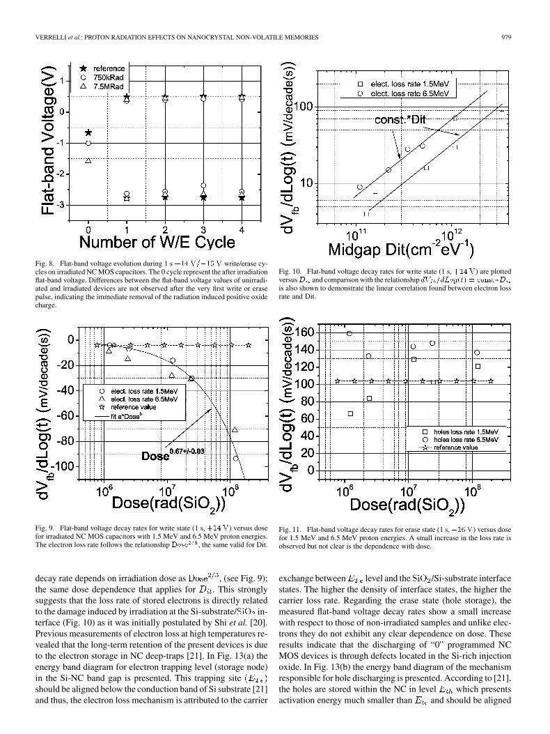
VERRELLI et al.: PROTON RADIATION EFFECTS ON NANOCRYSTAL NON-VOLATILE MEMORIES 979
Fig. 8. Flat-band voltage evolution during 1 s +14 V=�16 V write/erase cy-cles on irradiated NC MOS capacitors. The 0 cycle represent the after irradiationflat-band voltage. Differences between the flat-band voltage values of unirradi-ated and irradiated devices are not observed after the very first write or erasepulse, indicating the immediate removal of the radiation induced positive oxidecharge.
Fig. 9. Flat-band voltage decay rates for write state (1 s, +14 V) versus dosefor irradiated NC MOS capacitors with 1.5 MeV and 6.5 MeV proton energies.The electron loss rate follows the relationship Dose , the same valid for Dit.
decay rate depends on irradiation dose as , (see Fig. 9);the same dose dependence that applies for . This stronglysuggests that the loss rate of stored electrons is directly relatedto the damage induced by irradiation at the Si-substrate/ in-terface (Fig. 10) as it was initially postulated by Shi et al. [20].Previous measurements of electron loss at high temperatures re-vealed that the long-term retention of the present devices is dueto the electron storage in NC deep-traps [21]. In Fig. 13(a) theenergy band diagram for electron trapping level (storage node)in the Si-NC band gap is presented. This trapping siteshould be aligned below the conduction band of Si substrate [21]and thus, the electron loss mechanism is attributed to the carrier
Fig. 10. Flat-band voltage decay rates for write state (1 s, +14 V) are plottedversusD and comparison with the relationship dV =dLog(t) = const�Dis also shown to demonstrate the linear correlation found between electron lossrate and Dit.
Fig. 11. Flat-band voltage decay rates for erase state (1 s, �16V) versus dosefor 1.5 MeV and 6.5 MeV proton energies. A small increase in the loss rate isobserved but not clear is the dependence with dose.
exchange between level and the /Si-substrate interfacestates. The higher the density of interface states, the higher thecarrier loss rate. Regarding the erase state (hole storage), themeasured flat-band voltage decay rates show a small increasewith respect to those of non-irradiated samples and unlike elec-trons they do not exhibit any clear dependence on dose. Theseresults indicate that the discharging of “0” programmed NCMOS devices is through defects located in the Si-rich injectionoxide. In Fig. 13(b) the energy band diagram of the mechanismresponsible for hole discharging is presented. According to [21],the holes are stored within the NC in level which presentsactivation energy much smaller than and should be aligned
980 IEEE TRANSACTIONS ON NUCLEAR SCIENCE, VOL. 54, NO. 4, AUGUST 2007
Fig. 12. Memory window evolution with time for 1.5 MeV protons irradiatedNC MOS capacitors. Memory window for unirradiated devices is also indicated.The dashed line is the V of fresh unirradiated devices. These results appliesalso for 6.5 MeV irradiations.
Fig. 13. Energy band diagram for a NC charged with (a) electron and (b) holesrespectively, showing the mechanisms responsible for charge loss.
below the valence band of Si substrate. As a consequence, thehole loss mechanism does not involve /Si-substrate inter-face states but is based on the trap-to-trap conduction throughthe Si-rich injection oxide where two type of oxide traps exist.The first type comprises the traps formed due to the excess Siatoms or clusters that remain after the formation process of theNCs. The second type of traps are the radiation induced defects.The latter has a density of the order of while theformer should have a density of the order of the Si implantationdose, thus many orders higher than the radiation induced defectdensity. This in turns is believed to be the reason of the observedweak dependence of the holes flat-band voltage decay rate ontoirradiation dose.
Compared to unirradiated NC devices, the 10-yrs reductionin extrapolated memory window of irradiated NC devices doesnot exceed 30% (worst case of samples irradiated with 120 Mrad
).
Fig. 14. Memory behavior obtained after 30 ms write (positive) pulses anderase (negative) pulses on unirradiated NC nMOS transistors.
Fig. 15. threshold voltage measured after irradiation for charged (write)transistors.
B. Transistors
Charge injection into the NCs by FN tunneling results in ashift of the transistor transfer characteristics, . Thememory window of the unirradiated NC nMOS transistors wasdetermined after application of 30 ms square voltage pulseswith height ranging from 0 to . The maximum thresholdshifts are observed for pulses of (full write) and(full erase), leading to a memory window of 2.3 V as shownin Fig. 14. These unirradiated transistors show a 10-yrs extrap-olated memory window of . After write/erase cy-cles (endurance measurement) no degradation in the memorywindow was detected [17].
As found for the NC MOS capacitors, the radiation inducedoxide charge can be easily removed by electric field stressing(for example 1 write or erase pulse).
No bit flip has been observed on charged (write state) de-vices as shown in Fig. 15. Comparing the shifts observedfor the programmed NC MOS capacitors with the shifts forprogrammed NC nMOS transistors it can be concluded that forthe latter devices the effect of radiation induced positive charge
VERRELLI et al.: PROTON RADIATION EFFECTS ON NANOCRYSTAL NON-VOLATILE MEMORIES 981
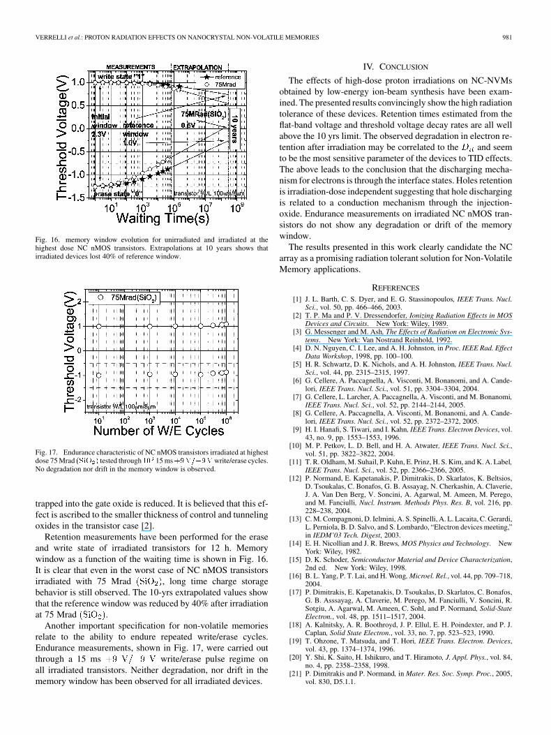
Fig. 16. memory window evolution for unirradiated and irradiated at thehighest dose NC nMOS transistors. Extrapolations at 10 years shows thatirradiated devices lost 40% of reference window.
Fig. 17. Endurance characteristic of NC nMOS transistors irradiated at highestdose 75 Mrad (SiO ) tested through 10 15 ms+9V=�9Vwrite/erase cycles.No degradation nor drift in the memory window is observed.
trapped into the gate oxide is reduced. It is believed that this ef-fect is ascribed to the smaller thickness of control and tunnelingoxides in the transistor case [2].
Retention measurements have been performed for the eraseand write state of irradiated transistors for 12 h. Memorywindow as a function of the waiting time is shown in Fig. 16.It is clear that even in the worst case of NC nMOS transistorsirradiated with 75 Mrad , long time charge storagebehavior is still observed. The 10-yrs extrapolated values showthat the reference window was reduced by 40% after irradiationat 75 Mrad .
Another important specification for non-volatile memoriesrelate to the ability to endure repeated write/erase cycles.Endurance measurements, shown in Fig. 17, were carried outthrough a 15 ms write/erase pulse regime onall irradiated transistors. Neither degradation, nor drift in thememory window has been observed for all irradiated devices.
IV. CONCLUSION
The effects of high-dose proton irradiations on NC-NVMsobtained by low-energy ion-beam synthesis have been exam-ined. The presented results convincingly show the high radiationtolerance of these devices. Retention times estimated from theflat-band voltage and threshold voltage decay rates are all wellabove the 10 yrs limit. The observed degradation in electron re-tention after irradiation may be correlated to the and seemto be the most sensitive parameter of the devices to TID effects.The above leads to the conclusion that the discharging mecha-nism for electrons is through the interface states. Holes retentionis irradiation-dose independent suggesting that hole dischargingis related to a conduction mechanism through the injection-oxide. Endurance measurements on irradiated NC nMOS tran-sistors do not show any degradation or drift of the memorywindow.
The results presented in this work clearly candidate the NCarray as a promising radiation tolerant solution for Non-VolatileMemory applications.
REFERENCES
[1] J. L. Barth, C. S. Dyer, and E. G. Stassinopoulos, IEEE Trans. Nucl.Sci., vol. 50, pp. 466–466, 2003.
[2] T. P. Ma and P. V. Dressendorfer, Ionizing Radiation Effects in MOSDevices and Circuits. New York: Wiley, 1989.
[3] G. Messenger and M. Ash, The Effects of Radiation on Electronic Sys-tems. New York: Van Nostrand Reinhold, 1992.
[4] D. N. Nguyen, C. I. Lee, and A. H. Johnston, in Proc. IEEE Rad. EffectData Workshop, 1998, pp. 100–100.
[5] H. R. Schwartz, D. K. Nichols, and A. H. Johnston, IEEE Trans. Nucl.Sci., vol. 44, pp. 2315–2315, 1997.
[6] G. Cellere, A. Paccagnella, A. Visconti, M. Bonanomi, and A. Cande-lori, IEEE Trans. Nucl. Sci., vol. 51, pp. 3304–3304, 2004.
[7] G. Cellere, L. Larcher, A. Paccagnella, A. Visconti, and M. Bonanomi,IEEE Trans. Nucl. Sci., vol. 52, pp. 2144–2144, 2005.
[8] G. Cellere, A. Paccagnella, A. Visconti, M. Bonanomi, and A. Cande-lori, IEEE Trans. Nucl. Sci., vol. 52, pp. 2372–2372, 2005.
[9] H. I. Hanafi, S. Tiwari, and I. Kahn, IEEE Trans. Electron Devices, vol.43, no. 9, pp. 1553–1553, 1996.
[10] M. P. Petkov, L. D. Bell, and H. A. Atwater, IEEE Trans. Nucl. Sci.,vol. 51, pp. 3822–3822, 2004.
[11] T. R. Oldham, M. Suhail, P. Kuhn, E. Prinz, H. S. Kim, and K. A. Label,IEEE Trans. Nucl. Sci., vol. 52, pp. 2366–2366, 2005.
[12] P. Normand, E. Kapetanakis, P. Dimitrakis, D. Skarlatos, K. Beltsios,D. Tsoukalas, C. Bonafos, G. B. Assayag, N. Cherkashin, A. Claverie,J. A. Van Den Berg, V. Soncini, A. Agarwal, M. Ameen, M. Perego,and M. Fanciulli, Nucl. Instrum. Methods Phys. Res. B, vol. 216, pp.228–238, 2004.
[13] C. M. Compagnoni, D. Ielmini, A. S. Spinelli, A. L. Lacaita, C. Gerardi,L. Perniola, B. D. Salvo, and S. Lombardo, “Electron devices meeting,”in IEDM’03 Tech. Digest, 2003.
[14] E. H. Nicollian and J. R. Brews, MOS Physics and Technology. NewYork: Wiley, 1982.
[15] D. K. Schoder, Semiconductor Material and Device Characterization,2nd ed. New York: Wiley, 1998.
[16] B. L. Yang, P. T. Lai, and H. Wong, Microel. Rel., vol. 44, pp. 709–718,2004.
[17] P. Dimitrakis, E. Kapetanakis, D. Tsoukalas, D. Skarlatos, C. Bonafos,G. B. Asssayag, A. Claverie, M. Perego, M. Fanciulli, V. Soncini, R.Sotgiu, A. Agarwal, M. Ameen, C. Sohl, and P. Normand, Solid-StateElectron., vol. 48, pp. 1511–1517, 2004.
[18] A. Kalnitsky, A. R. Boothroyd, J. P. Ellul, E. H. Poindexter, and P. J.Caplan, Solid State Electron., vol. 33, no. 7, pp. 523–523, 1990.
[19] T. Ohzone, T. Matsuda, and T. Hori, IEEE Trans. Electron. Devices,vol. 43, pp. 1374–1374, 1996.
[20] Y. Shi, K. Saito, H. Ishikuro, and T. Hiramoto, J. Appl. Phys., vol. 84,no. 4, pp. 2358–2358, 1998.
[21] P. Dimitrakis and P. Normand, in Mater. Res. Soc. Symp. Proc., 2005,vol. 830, D5.1.1.