powerpoint 演示文稿 - arxiv
TRANSCRIPT
Interaction between the small gas molecules and the defective WSe2 monolayer
Dongwei Ma1,, Chaozheng He2,, Benyuan Ma2, Zhiwen Lu2,Yanan Tang3,,
Zhansheng Lu4 and Zongxian Yang4
1School of Physics, Anyang Normal University, Anyang 455000, China
2Physics and Electronic Engineering College, Nanyang Normal University, Nanyang
473061, China
3College of Physics and Electronic Engineering, Zhengzhou Normal University,
Zhengzhou, 450044, China
4College of Physics and Materials Science, Henan Normal University, Xinxiang
453007, China
Abstract
In this study, the interaction between the gas molecules, including H2O, N2, CO,
NO, NO2 and N2O, with the WSe2 monolayer containing a Se vacancy (denoted as VSe)
is theoretically studied. It is found that H2O and N2 molecules are highly prone to be
physisorbed on the VSe surface. The presence of the Se vacancy should significantly
enhance the sensing ability of the WSe2 monolayer toward the H2O and N2 molecules.
In contrast, CO and NO molecules highly prefer to be molecularly chemisorbed on the
VSe surface with the non-oxygen atom occupying the Se site. Further, the exposed O
atoms of the molecularly chemisorbed CO or NO can be reacted with the additional CO
or NO molecule, to produce the C-doped or N-doped WSe2 monolayer. Our electronic
structure calculations show that the WSe2 monolayers are p-doped by the CO and NO
molecules, as well as the C and N atoms. The calculated energies suggest that the filling
of the CO or NO molecule and the removal of the exposed O atom by the additional
CO or NO molecule are both energetically and dynamically favorable. However, only
the NO molecule and N atom doped WSe2 monolayers exhibit significantly improved
electronic structures compared with the defective WSe2 monolayer. The NO2 and N2O
molecules will dissociate directly to form a O-doped WSe2 with a physisorbed NO or
Corresponding author. E-mail: [email protected] (Dongwei Ma). Corresponding author. E-mail: [email protected] (Chaozheng He). Corresponding author. E-mail: [email protected] (Yanan Tang).
N2. After desorbing the physisorbed NO or N2, the O-doped WSe2 monolayer can be
obtained, for which the defect levels due to the Se vacancy can be completely removed.
The calculated energies suggest that although the dissociation processes for NO2 and
N2O molecules are highly endothermic, the N2O dissociation may need to operate at an
elevated temperature compared with the room temperature, due to its large energy
barrier of ~ 1 eV.
Keywords:
First-principles calculation, WSe2 monolayer, Se vacancy, molecular adsorption,
electronic structure
.
1. Introduction
Investigations on the excellent properties of graphene have stimulated great
interest in exploring novel properties and applications of other two-dimensional (2D)
layered materials. Graphene is known having an intrinsic zero bandgap, which has
hindered significantly its application in logical electronic devices.[1] The layered
transition metal dichalcogenides (TMDs) have gained numerous attention in recent
years due to its exciting physical and chemical properties.[2-4] Especially, group 6
TMDs, such as WSe2 and MoS2, present remarkable features, such as indirect-to-direct
bandgap crossover,[5, 6] layer-dependent tunable bandgap,[5, 7] valley-selective
optical excitation,[8, 9] and topological superconductivity[10]. These unique properties
make TMDs great promising in the fields of field-effect transistors,[7, 11] flexible
electronics,[6, 12] optoelectonics,[13, 14] valleytronics,[15, 16] and electrocatalysts
and photocatalysts[17].
WSe2 monolayer has a direct bandgap of ~ 1.6 eV, which is smaller than that of
MoS2 monolayer (~ 1.8 eV).[18] MoS2 mostly exhibits unipolar n-type transport
characteristics resulting from the pronounced Fermi level pinning effect at the interface
between metal and MoS2.[19] On the contrary, WSe2 can achieve electron-dominated,
ambipolar, and hole-dominated transport behaviors by engineering the number of
layers[20] and simply choosing a suitable contact metal[21, 22]. Field effect transistor
experiments have shown respectable mobility values of WSe2 for electrons (110 cm2V-
1S-1)[23] and holes (240 cm2V-1S-1)[24]. The unique electronic properties, and other
excellent attributes have led to a significant increase of the research interest in WSe2
recently.[9, 25, 26]
Due to their atomic thickness, 2D layered semiconductors have inherent large
surface-to-volume ratio, which is highly favorable for the gas molecule adsorption and
surface-related applications, such as catalysis, sensing, and doping.[17, 27, 28] It is
noted that defects with dangling or strained bonds often exhibit much enhanced
chemical activity towards the adsorbates compared with the perfect lattice sites.[29-32]
For TMD 2D semiconductors, there are have lots of studies investigating the interaction
between the common gas molecules (such as H2O, O2, N2, CO, NO, NO2) and the
perfect or defective MoS2 monolayer, both experimentally[33-37] and theoretically[29,
38-44].
It is known that chalcogen vacancies are the most commonly occurring point
defects in most TMDs. These chalcogen vacancies can create deep acceptor states that
act as efficient electron traps and limit the electron mobility.[45-49] Previous reports
have shown that the interaction of common gas molecules with the chalocogen
vacancies can improve the electronic properties of the as-prepared MoS2. For example,
the strong photoluminescence enhancement of the MoS2 monolayer has been observed
through defect engineering and oxygen bonding, which is probably formed by the
adsorption of O2 molecules at the S vacancies of MoS2.[29, 50, 51] The S vacancies
can also be repaired by CO, NO, or NO2 molecules, according to the first-principles
calculations based on density functional theory (DFT).[42] On the other hand, the S
vacancies may have a beneficial effect for other applications. For example, DFT
calculations predicted that the S vacancies can improve the sensing of the common gas
molecules.[43, 44] A combination of experimental and theoretical study indicates that
the S vacancy allow us to achieve the highest hydrogen evolution reaction activity
among all the MoS2 catalyst.[37]
For WSe2, to our knowledge, there are few studies on the interaction between the
common gas molecules with its surfaces. WSe2 monolayer has been p-doped using NO2,
as revealed by the field-effect transistor experiment.[24] Ovcharenko et al. found a

weak adsorption of NO2 on the WSe2 surface and a slight change of the electronic
structure of the material by DFT and photoelectron spectroscopy studies.[52] Zhao et
al. explored the p-doping of WSe2 via chemisorption of NO2 at a sample temperature
of 150 ℃. The DFT calculations and spectroscopy results has identified the
chemisorbed NO as the dominant doping species at the Se vacancies sites with the N
atom occupying the vacancy.[53] Theoretically, Liu et al. studied the transition from
chemisorption to physisorption (PS) states of O2 on the WSe2 monolayer with a single
Se vacancy (denoted as VSe),[29] while Zhao et al. studied the dissociation of the
chemisorbed O2 on the VSe surface.[54] The adsorption of several common gas
molecules has been studied by Wang et al.[55] on the pristine WSe2 surface (p-WSe2).
In this study, we investigated the effect of Se vacancies on the interaction between
the gas molecules, including H2O, N2, CO, NO, NO2 and N2O, with the WSe2
monolayer surfaces. Our study reveals a markedly different interaction behavior of the
various gas molecules on the VSe surfaces. For example, the H2O and N2 molecules are
highly prone to be physisorbed on the VSe surface. In contrast, CO and NO molecules
highly prefer to be molecularly chemisorbed on the VSe surface with the non-oxygen
atom occupying the Se site. Further, the exposed O atoms of the molecularly
chemisorbed CO or NO can be reacted with the additional CO or NO molecule, to
produce the C-doped or N-doped WSe2 monolayer. The NO2 or N2O molecules will
dissociate directly to form a O-doped WSe2 with a physisorbed NO or N2. In the
following, the energies, geometric structures and electronic structure of the different
adsorption states for various molecules will be presented and discussed. It is hoped our
study will give novel insight into the doping of WSe2 via the interaction between
common gas molecules and the Se vacancy, and also reveal the possible application of
the defective WSe2 in the gas sensing field.
2. Computational details
First-principles calculations have been performed using the projected augmented
wave formalism of DFT, as implemented in the Vienna Ab-initio Simulation Package
(VASP).[56-58] To correctly describe the effect of the van der Waals (vdW) interaction
between the adsorbed molecule and the WSe2 monolayer, the optB86b-vdW exchange
functional is adopted for the vdW correction,[59, 60] which has been used for the MoS2
systems recently.[61-63] The cutoff energy for the plane-wave basis set is taken as 450
eV. With these settings, the calculated lattice parameter of the WSe2 monolayer is 3.295
Å, which is in good agreement with the previous theoretical values of 3.29 Å[64] and
3.298[65]. Band structure calculations show that the pristine WSe2 monolayer is an
direct bandgap semiconductor with the bandgap of 1.62 eV, which is also in agreement
with previous theoretical (1.60 eV)[64] and experimental (1.65 eV) results.[66]
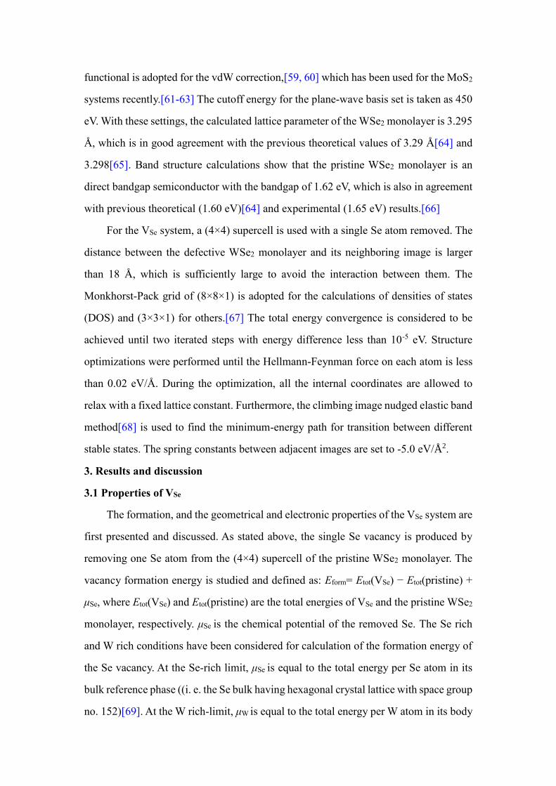
For the VSe system, a (4×4) supercell is used with a single Se atom removed. The
distance between the defective WSe2 monolayer and its neighboring image is larger
than 18 Å, which is sufficiently large to avoid the interaction between them. The
Monkhorst-Pack grid of (8×8×1) is adopted for the calculations of densities of states
(DOS) and (3×3×1) for others.[67] The total energy convergence is considered to be
achieved until two iterated steps with energy difference less than 10-5 eV. Structure
optimizations were performed until the Hellmann-Feynman force on each atom is less
than 0.02 eV/Å. During the optimization, all the internal coordinates are allowed to
relax with a fixed lattice constant. Furthermore, the climbing image nudged elastic band
method[68] is used to find the minimum-energy path for transition between different
stable states. The spring constants between adjacent images are set to -5.0 eV/Å2.
3. Results and discussion
3.1 Properties of VSe
The formation, and the geometrical and electronic properties of the VSe system are
first presented and discussed. As stated above, the single Se vacancy is produced by
removing one Se atom from the (4×4) supercell of the pristine WSe2 monolayer. The
vacancy formation energy is studied and defined as: Eform= Etot(VSe) − Etot(pristine) +
μSe, where Etot(VSe) and Etot(pristine) are the total energies of VSe and the pristine WSe2
monolayer, respectively. μSe is the chemical potential of the removed Se. The Se rich
and W rich conditions have been considered for calculation of the formation energy of
the Se vacancy. At the Se-rich limit, μSe is equal to the total energy per Se atom in its
bulk reference phase ((i. e. the Se bulk having hexagonal crystal lattice with space group
no. 152)[69]. At the W rich-limit, μW is equal to the total energy per W atom in its body
center cubic bulk phase, while μSe has been calculated by μWSe2 = μW + 2μSe (μWSe2 equal
to total energy per formula unit of the pristine monolayer WSe2). With such a definition,
defect with low formation energies will occur in high concentrations.[70] The
calculated vacancy formation energy at the W-rich limit is 2.04 eV, which is close to
the result (~ 1.8 eV) in Ref.[70]. For the Se-rich limit, the formation energy for the Se
vacancy is 2.09 eV. This value is much smaller than the result (~ 2.7 eV) of Ref.[70],
which may result from different Se bulk reference phase has been used. Nevertheless,
the calculated formation energies for the Se vacancy are comparable to the S vacancy
in the MoS2 monolayer. For example, Liu et al. predicted that the formation energies of
a S vacancy at the S-poor and S-rich limits are 2.35 and 0.95 eV, respectively.[71] The
formation energy by Haldar et al. lies between about 1.3 and 2.6 eV depending on the
chemical potential of the element S.[70] This suggests that the equilibrium
concentrations of the Se vacancy in the WSe2 monolayer should be similar to those of
the S vacancy in the monolayer MoS2. Consequently, the presence of the Se vacancy
will also play an important role in the electronic and optical properties of 2D WSe2
semiconductors, similar to the role of S vacancies in the monolayer MoS2
electronics,[72] which has been demonstrated in the experimental studies.[53, 73-75]
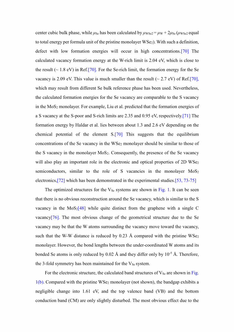
The optimized structures for the VSe systems are shown in Fig. 1. It can be seen
that there is no obvious reconstruction around the Se vacancy, which is similar to the S
vacancy in the MoS2[48] while quite distinct from the graphene with a single C
vacancy[76]. The most obvious change of the geometrical structure due to the Se
vacancy may be that the W atoms surrounding the vacancy move toward the vacancy,
such that the W-W distance is reduced by 0.23 Å compared with the pristine WSe2
monolayer. However, the bond lengths between the under-coordinated W atoms and its
bonded Se atoms is only reduced by 0.02 Å and they differ only by 10-5 Å. Therefore,
the 3-fold symmetry has been maintained for the VSe system.
For the electronic structure, the calculated band structures of VSe are shown in Fig.
1(b). Compared with the pristine WSe2 monolayer (not shown), the bandgap exhibits a
negligible change into 1.61 eV, and the top valence band (VB) and the bottom
conduction band (CM) are only slightly disturbed. The most obvious effect due to the

Se vacancy is that there are flat defect states appearing ~ 0.4 eV below the bottom of
the CM, which is typical for most TMDs. The total DOS for VSe and the local DOS
(LDOS) projected on the W atoms surrounding the Se vacancy are shown in Fig. 1(c).
The LDOS indicates that the deep acceptor states in the bandgap originate from the W
dangling bonds (5d states). As stated in the previous studies, such levels can reduce the
carrier mobility, by trapping or scattering other charge carriers, and lead to a decrease
of the quantum efficiency of the material.[29, 49, 74] On the other hand, the dangling
bonds often exhibit high chemical activity towards the external adsorbates, compared
with the perfect lattice sites,[29-32] which may provide new opportunities for doping
of materials, and their applications in surface-related applications, such as sensing and
catalysis.
3.2 Physisorption of H2O and N2 molecules
To study the adsorption stability of the considered molecules on the defective
WSe2 monolayer, the adsorption energy is defined as: Ead = Evac + Emol – Evac-mol, where
Evac and Evac-mol are the total energies of the defective WSe2 monolayers without and
with the adsorbed molecules, respectively, and Emol is the total energy of the free
molecule. With this definition, a positive value of the adsorption energy indicates that
the process is exothermic and energetically favorable. For the adsorption of gas
molecules, three adsorption states have been considered for each molecule, i.e., PS,
molecular chemisorption (MC), and dissociative chemisorption (DC). The calculated
adsorption energies for all the considered molecules at the available states are shown in
Table 1.
For H2O molecules, it is found that the molecule can only be physisorbed above
the surface of VSe. If the molecule is put into the vacancy in the initial configuration, it
will run away from the vacancy site after structural optimization. The optimized
structures for H2O adsorption on VSe are shown in Fig. 2(a). The H2O molecule is 0.88
Å away from the surface and adopts a vertical configuration, where one O-H bond is
almost perpendicular to the WSe2 basal plane with the H atom pointing to the Se
vacancy site. Such configuration is different from the cases of H2O molecule adsorption
on the perfect MoS2 and WSe2 monolayers (as presented in Fig. S1 (a) of the Electronic
Supporting Information (ESI)), where the axis that connects two H atoms is parallel to
the basal planes of the monolayer sheets. The H-O-H bond angle is reduced by 0.2⁰.
The bond length of the O-H bond almost perpendicular to the WSe2 surface is elongated
by 0.01 Å, while another O-H bond is almost unchanged. In addition, the calculated
adsorption energy for H2O molecules is 0.30 eV. These results suggest that the H2O
molecule is physisorbed on the surface of VSe. For the N2 molecule, except the PS state,
the MC state can be also obtained. However, the MC state is endothermic by 0.08 eV
and is less stable than the PS state by 0.25 eV. Thus, we only focus on the PS state. The
optimized structures for N2 adsorption on VSe are shown in Fig. 2(b). The distance
between the N2 molecule and the surface of VSe is 2.39 Å, much larger than that for
H2O. Accordingly, the N2 molecule (0.17 eV) has a much smaller adsorption energy
than the H2O molecule (0.30 eV).
To make a comparison, we also performed studies on the adsorption of H2O and
O2 molecules on the pristine WSe2 monolayer. Different adsorption sites are considered
for the adsorption of the molecules with various initial molecule orientations. The
optimized structures for the most stable ones are shown in Fig. S(1) of ESI. It is clear
that the Se vacancy can greatly enhance the adsorption strength of H2O and N2
molecules. For H2O molecules, the adsorption energy on VSe is larger than that on the
pristine WSe2 monolayer by 67%, and the distances between the molecule and the basal
plane of the pristine WSe2 is larger than that of VSe by 1.7 Å. For N2 molecules, the Se
vacancy increases the adsorption strength by 0.05 eV.
Previously, it is proposed that the physisorbed gas molecules can be detected
sensitively through a charge transfer mechanism by the TMDs and other 2D materials.
Therefore, we calculated the charge transfer between the adsorbed molecules and the
WSe2 monolayer by using Bader charge analysis. It is shown than H2O molecules gain
electrons of 0.06 e from VSe, which is much larger than that from the pristine WSe2
monolayer (0.02 e). The enhanced charge transfer is also observed for N2 molecules.
However, it is noted that the H2O molecules act as electron acceptors, while the N2
molecules as electron donors. Apart from the enhanced charge transfer, the charge
density differences (CDDs) are also studied. The CDD are calculated with respect to
the adsorbed molecule and the defective WSe2 support with the configuration in the
adsorbed system. Compared with results presented in Fig. 2 and Fig. S1, it is obvious
that the Se vacancy can also enhance the charge redistribution due to the adsorption of
the molecule. Overall, the VSe system exhibits a significantly enhanced sensing ability
toward the H2O and N2 molecules, as indicative of the enhanced adsorption energy,
charge transfer, and charge redistribution. In addition, we also studied the electronic
structure of the adsorbed systems, in terms of band structures and DOS (not shown).
Our results reveal that the electronic states are almost unchanged upon the adsorption
of molecules, for both the pristine and the defective WSe2 monolayers.
3.3 Chemisorption of CO, NO, NO2 and N2O molecules
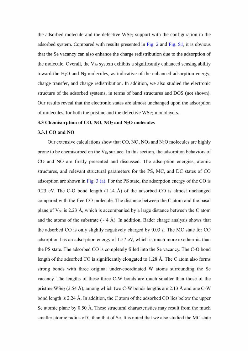
3.3.1 CO and NO
Our extensive calculations show that CO, NO, NO2 and N2O molecules are highly
prone to be chemisorbed on the VSe surface. In this section, the adsorption behaviors of
CO and NO are firstly presented and discussed. The adsorption energies, atomic
structures, and relevant structural parameters for the PS, MC, and DC states of CO
adsorption are shown in Fig. 3 (a). For the PS state, the adsorption energy of the CO is
0.23 eV. The C-O bond length (1.14 Å) of the adsorbed CO is almost unchanged
compared with the free CO molecule. The distance between the C atom and the basal
plane of VSe is 2.23 Å, which is accompanied by a large distance between the C atom
and the atoms of the substrate (~ 4 Å). In addition, Bader charge analysis shows that
the adsorbed CO is only slightly negatively charged by 0.03 e. The MC state for CO
adsorption has an adsorption energy of 1.57 eV, which is much more exothermic than
the PS state. The adsorbed CO is completely filled into the Se vacancy. The C-O bond
length of the adsorbed CO is significantly elongated to 1.28 Å. The C atom also forms
strong bonds with three original under-coordinated W atoms surrounding the Se
vacancy. The lengths of these three C-W bonds are much smaller than those of the
pristine WSe2 (2.54 Å), among which two C-W bonds lengths are 2.13 Å and one C-W
bond length is 2.24 Å. In addition, the C atom of the adsorbed CO lies below the upper
Se atomic plane by 0.50 Å. These structural characteristics may result from the much
smaller atomic radius of C than that of Se. It is noted that we also studied the MC state
with the O atom occupying the Se vacancy. If is found that the filled CO molecule will
run away from the vacancy after fully structural optimization. The DC state has the
separated C atom occupying the Se vacancy and the O atom sitting above one
neighboring Se atom (Se-O bond length 1.68 Å), which can be considered as the C-
doped WSe2 monolayer with an adsorbed O atom on a Se atom neighboring the doped
C. However, this state is highly endothermic compared with the MC state by 2.60 eV.
Therefore, it is highly unfavorable for CO molecules to dissociate induced by the Se
vacancy. And, from an energetic point of view, the CO molecule will exist in the MC
state on VSe.
The interaction of NO molecules with the VSe surface is much stronger than that
of CO molecules. The adsorption energy of the NO for the PS state is 0.37 eV, larger
than that of the CO molecule by 0.14 eV. The N-O bond length of the adsorbed NO for
is elongated by 0.01 Å. The distance between the lower N atom of the adsorbed NO and
the upper Se atomic plane is 1.30 Å. There is also more electron transfer (0.11 e) for
the adsorbed NO than the adsorbed CO. The MC state for the NO adsorption is much
more stable than that for the CO adsorption, with the adsorption energy difference up
to ~ 1.6 eV between two states. The structural characteristics of the MC state for NO is
similar to those of that for CO, which will be not further discussed. In addition, the NO
molecule can adopt the configuration having the O atom occupying the Se vacancy,
however, for which the adsorption energy is only 0.35 eV. Contrary to the CO molecule,
the DC state for the NO adsorption is highly endothermic by 2.50 eV. This state can be
considered as the N-doped WSe2 monolayer with one O atom sitting above one Se atom
neighboring the doped N. Although the DC state for NO is endothermic with respect to
the free NO molecule, it is exothermic with respect to the MC state by ~ 0.7 eV. Further,
our CI-NEB calculation (not shown) indicates that the transition from the MC to the
DC states needs to overcome an energy barrier of 2.12 eV. Therefore, the NO molecule
will also exist in the MC state on VSe.
CDDs for the MC states of CO and NO molecules are also shown in Fig. 3 in order
to gain further insight into the interaction between the molecules and the supports. As
shown in Fig. 3(a), the transferred electrons are mainly localized on the C atom and the
C-W bonds, in agreement with the strong adsorption of CO. On the other hand, there is
electron depletion on the C-O bond, and thus the C-O bond has been significantly
weakened, which will make the O atom protruding above the S plane chemically active
towards other reducing molecules, including CO itself. The CDD of the MC state for
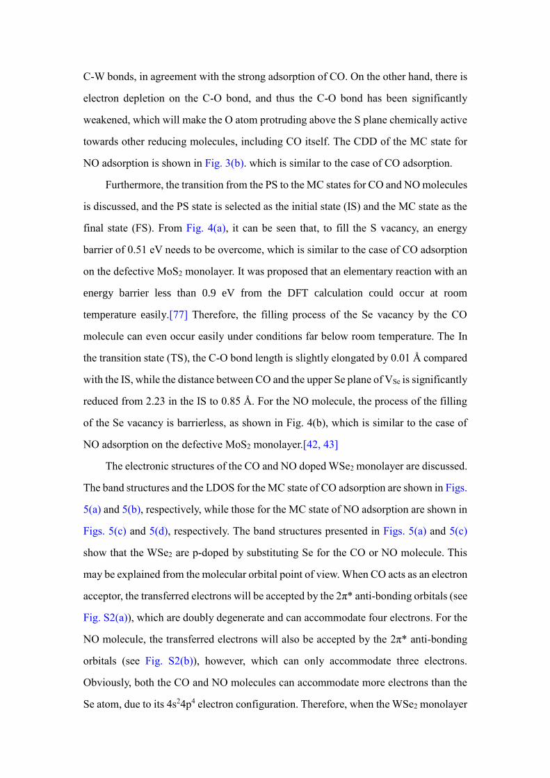
NO adsorption is shown in Fig. 3(b). which is similar to the case of CO adsorption.
Furthermore, the transition from the PS to the MC states for CO and NO molecules
is discussed, and the PS state is selected as the initial state (IS) and the MC state as the
final state (FS). From Fig. 4(a), it can be seen that, to fill the S vacancy, an energy
barrier of 0.51 eV needs to be overcome, which is similar to the case of CO adsorption
on the defective MoS2 monolayer. It was proposed that an elementary reaction with an
energy barrier less than 0.9 eV from the DFT calculation could occur at room
temperature easily.[77] Therefore, the filling process of the Se vacancy by the CO
molecule can even occur easily under conditions far below room temperature. The In
the transition state (TS), the C-O bond length is slightly elongated by 0.01 Å compared
with the IS, while the distance between CO and the upper Se plane of VSe is significantly
reduced from 2.23 in the IS to 0.85 Å. For the NO molecule, the process of the filling
of the Se vacancy is barrierless, as shown in Fig. 4(b), which is similar to the case of
NO adsorption on the defective MoS2 monolayer.[42, 43]
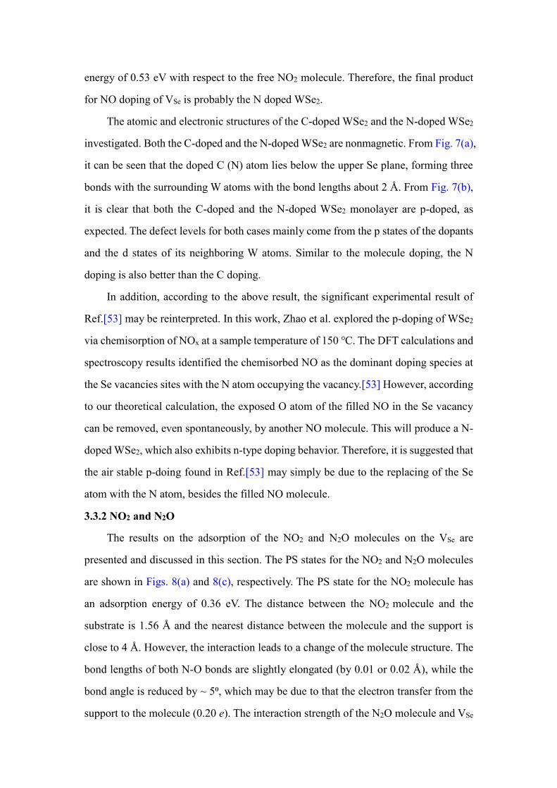
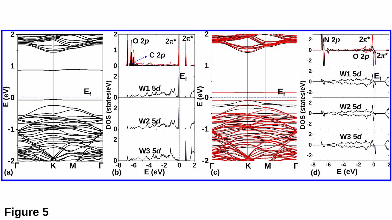
The electronic structures of the CO and NO doped WSe2 monolayer are discussed.
The band structures and the LDOS for the MC state of CO adsorption are shown in Figs.
5(a) and 5(b), respectively, while those for the MC state of NO adsorption are shown in
Figs. 5(c) and 5(d), respectively. The band structures presented in Figs. 5(a) and 5(c)
show that the WSe2 are p-doped by substituting Se for the CO or NO molecule. This
may be explained from the molecular orbital point of view. When CO acts as an electron
acceptor, the transferred electrons will be accepted by the 2π* anti-bonding orbitals (see
Fig. S2(a)), which are doubly degenerate and can accommodate four electrons. For the
NO molecule, the transferred electrons will also be accepted by the 2π* anti-bonding
orbitals (see Fig. S2(b)), however, which can only accommodate three electrons.
Obviously, both the CO and NO molecules can accommodate more electrons than the
Se atom, due to its 4s24p4 electron configuration. Therefore, when the WSe2 monolayer

is doped by substituting Se atom for the CO or NO molecule, it will exhibit a p-type
doping behavior. However, it is noted that the CO molecule may be not appropriate for
doping the WSe2, as the defect level still belongs to the deep acceptor level.
The LDOS of the C and O atoms, and the three W atoms marked in Fig. 3(a) are
shown in Fig. 5(c). It can be seen that the defect level below the Fermi level (Ef) mainly
comes from the O and C 2p states (the 2π* orbitals of the CO), and the W1 and W2 5d
states, while the W3 5d states make an important contribution to the defect level above
the Ef, except the 2π* orbitals of the CO. The MC state for the NO adsorption is
magnetic with a spin magnetic moment of 1.00 μB. There is one defect level for the
spin-up state and two defect levels for the spin-down states, which also mainly comes
from the 2π* orbitals of the adsorbed molecule and the 5d states of the W atoms bonded
with the N atom. Finally, Bader charge analysis shows that the adsorbed CO and NO
molecules have gained electrons of 2.22 and 1.49 e, respectively. This is in agreement
with the fact that upon adsorption considerable empty 2π* orbitals of the both molecules
shift down below the Ef.
It is meaningful and necessary to see if the adsorbed CO (NO) molecule in the MS
state can react with further injected molecules. For such purpose, the interaction of the
second CO (NO) molecule with the preadsorbed CO (NO) molecule on the VSe surface
is studied. For the CO molecule, it can be physisorbed above the preadsorbed CO
molecule (the IS in Fig. 6), and it can also combine with the O atom of the preadsobred
CO to form a physisorbed CO2 above the C doped WSe2 monolayer (the FS in Fig. 6).
Our CI-NEB calculation shows that the transition between two states needs to overcome
an energy barrier of 0.89 eV. For the FS, the calculated adsorption energy is 0.29 eV,
with respect to the free CO2 molecule. Therefore, it is very easy for the formed CO2 to
desorb from the C doped WSe2, leaving a C doped WSe2 monolayer. For NO, it is found
that even if initially the molecule is away from the surface by a distance up to 2.9 Å
(Fig. S3(a)), after optimization it still can directly combine with the O atom of the
preadsobred NO molecule to produce a physisorbed NO2 molecule above the N doped
WSe2 monolayer (Fig. S3(a)). Energetically, the state in Fig. S3(b) is more stable by
1.26 eV than the state shown in Fig. S3(a). And the state in Fig. S3(b) has an adsorption
energy of 0.53 eV with respect to the free NO2 molecule. Therefore, the final product
for NO doping of VSe is probably the N doped WSe2.
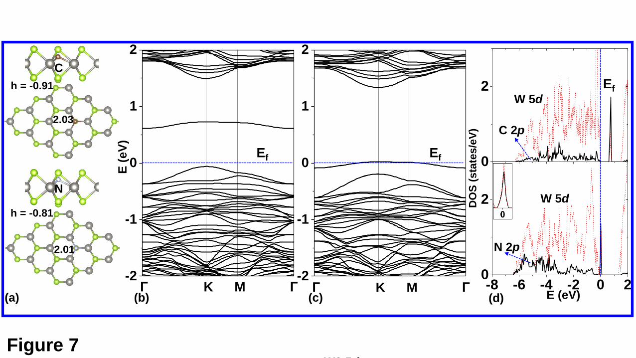
The atomic and electronic structures of the C-doped WSe2 and the N-doped WSe2
investigated. Both the C-doped and the N-doped WSe2 are nonmagnetic. From Fig. 7(a),
it can be seen that the doped C (N) atom lies below the upper Se plane, forming three
bonds with the surrounding W atoms with the bond lengths about 2 Å. From Fig. 7(b),
it is clear that both the C-doped and the N-doped WSe2 monolayer are p-doped, as
expected. The defect levels for both cases mainly come from the p states of the dopants
and the d states of its neighboring W atoms. Similar to the molecule doping, the N
doping is also better than the C doping.
In addition, according to the above result, the significant experimental result of
Ref.[53] may be reinterpreted. In this work, Zhao et al. explored the p-doping of WSe2
via chemisorption of NOx at a sample temperature of 150 ℃. The DFT calculations and
spectroscopy results identified the chemisorbed NO as the dominant doping species at
the Se vacancies sites with the N atom occupying the vacancy.[53] However, according
to our theoretical calculation, the exposed O atom of the filled NO in the Se vacancy
can be removed, even spontaneously, by another NO molecule. This will produce a N-
doped WSe2, which also exhibits n-type doping behavior. Therefore, it is suggested that
the air stable p-doing found in Ref.[53] may simply be due to the replacing of the Se
atom with the N atom, besides the filled NO molecule.
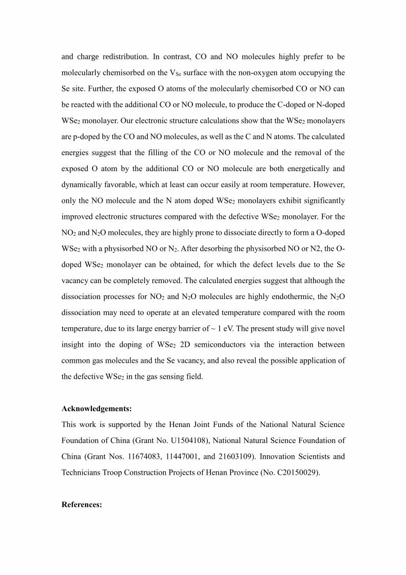
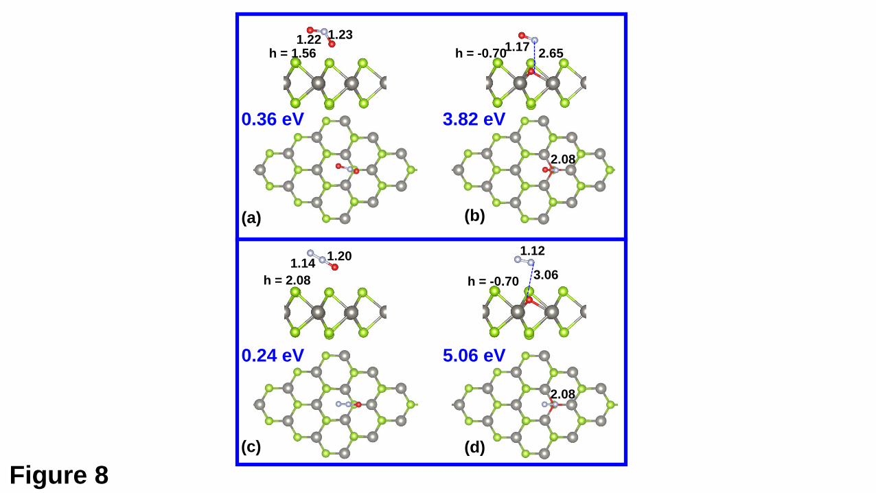
3.3.2 NO2 and N2O
The results on the adsorption of the NO2 and N2O molecules on the VSe are
presented and discussed in this section. The PS states for the NO2 and N2O molecules
are shown in Figs. 8(a) and 8(c), respectively. The PS state for the NO2 molecule has
an adsorption energy of 0.36 eV. The distance between the NO2 molecule and the
substrate is 1.56 Å and the nearest distance between the molecule and the support is
close to 4 Å. However, the interaction leads to a change of the molecule structure. The
bond lengths of both N-O bonds are slightly elongated (by 0.01 or 0.02 Å), while the
bond angle is reduced by ~ 5⁰, which may be due to that the electron transfer from the
support to the molecule (0.20 e). The interaction strength of the N2O molecule and VSe

in the PS state is weaker than that of N2O. The PS state for the N2O molecule has an
adsorption energy of 0.24 eV. Accordingly, the distance between the N2O and the upper
Se plane (2.08 Å) is also large compared with the case of N2O adsorption. And there is
a minor electron transfer (0.03 e) to the adsorbed N2O molecule.
For the chemisorption, it is found that there are only DC states for both the NO2
and N2O molecules. As shown in Fig. 8(b), the adsorbed NO2 can completely dissociate
to form a O-doped WSe2 with an adsorbed NO molecule. The dissociation process is
endothermic by 3.82 eV with respect to the free NO2 molecule. The distance between
the adsorbed NO and the doped O atom is 2.65 Å, which can exclude the possibility of
NO forming chemical bond with the support. The bond length (1.17 Å) of the adsorbed
NO is hardly unchanged compared with the free molecule, further confirming its weak
adsorption. The adsorption energy for the NO molecule is also studied, with respect to
the free NO molecule and the O-doped WSe2 monolayer. An adsorption energy of 0.32
eV suggests that the physiorbed NO can be easily desorbed from the support, leaving a
O-doped WSe2 monolayer. For the DC state of the N2O molecule, as shown in Fig. 8(d),
the dissociation of the N2O molecule on VSe will produce a O-doped WSe2 with an
physisorbed N2 molecule. The N2O dissociation process is also highly endothermic (by
5.06 eV) with reference to the free molecule. The distance between the physisorbed N2
and the doped O atom is 3.06 Å, and the adsorption energy for the N2 is 0.20 eV. These
suggest that the upon N2O dissociation on the VSe, there will be a O-doped WSe2
monolayer, similar to the case of the NO2 adsorption. In addition, the possible
chemisorption state with the N atom of the N2O pointing down has also been studied
(Fig. S4). It is found that this state is much less stable than the state shown in Fig. 8(d)
by about 2.7 eV, thus, which will be not further investigated.
The processes of the transition from the PS state to the DC state are shown in Fig.
9(a) and 9(b), respectively, for the NO2 and N2O molecules. For the NO2 molecule (Fig.
9(a)), the dissociation process is highly endothermic by 3.46 eV and only needs to
overcome an energy barrier of 0.04 eV. For the TS, the adsorbed NO2 molecule is much
closer to the support than the IS, while the lower N-O bond is only elongated by 0.04
Å compared with the IS. For the N2O molecule, the dissociation process is much

energetically favorable than that for the NO2 molecule. However, the N2O molecule
needs to overcome a large energy barrier of 0.98 eV. This may be due to the geometric
structure of the TS for the N2O molecule. As shown in Fig. 9(b), in the TS, the N2O
molecule is significantly distorted compared with that in the IS. The N-O bond is
elongated by 0.12 Å and the molecule becomes bent having a bond angle of 149⁰.
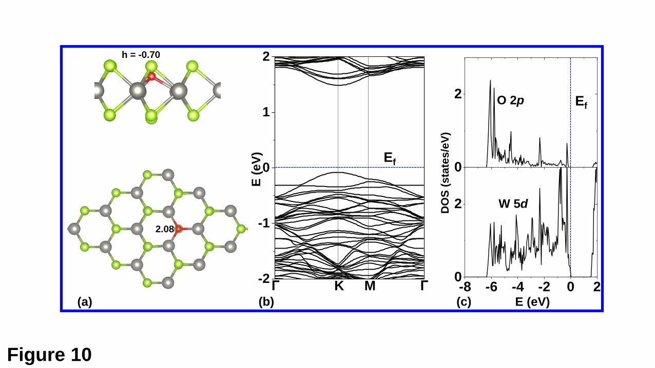
The geometric and electronic structures of the O-doped WSe2 are shown in Fig.
10. As shown in Fig. 10(a), the doped O atom lies about 0.70 Å below the upper S plane,
and forming three O-W bonds of 2.08 Å. The O-doped WSe2 monolayer is nonmagnetic.
The band structure shown in Fig. 10(b) shows that the defect levels induced by the Se
vacancy are completely removed, which is in good agreement with previous results.
The LDOS projected on the doped O and its bonded W show a significant hybridization
between the O 2p states and the W 5d states, revealing a strong interaction between two
species. Previously, a surface laser modification was proposed to passivate the Se
vacancy by O atoms, by which the conductivity and the photoconductivity are enhanced
by 400 and 150 times compared with the as-grown WSe2. Our studies suggest that
passivating Se vacancy by O atoms may be realized through a chemical route, by first
dosing NO2 or N2O gas onto the WSe2 surface and then heating the surface to desorb
the physisorbed NO or N2. It is noted that the produced N2 is safe, unlike NO, which is
toxic and harmful. Therefore, although for N2O the process needs to operate at an
elevated temperature compared with the room temperature, due to its large energy
barrier of ~ 1 eV, it is proposed that the N2O gas may be more favorable for healing the
Se vacancy than NO2.
4. Conclusions
In this study, we theoretically investigated the effect of Se vacancies on the
interaction between the gas molecules, including H2O, N2, CO, NO, NO2 and N2O, with
the WSe2 monolayer surfaces. According to the calculated energies, H2O and N2
molecules are highly prone to be physisorbed on the VSe surface. Compared with the
perfect lattice site, the presence of the Se vacancy can significantly enhance the sensing
ability of the WSe2 monolayer toward the H2O and N2 molecules via a surface charge
transfer mechanism, as indicative of the enhanced adsorption energy, charge transfer,
and charge redistribution. In contrast, CO and NO molecules highly prefer to be
molecularly chemisorbed on the VSe surface with the non-oxygen atom occupying the
Se site. Further, the exposed O atoms of the molecularly chemisorbed CO or NO can
be reacted with the additional CO or NO molecule, to produce the C-doped or N-doped
WSe2 monolayer. Our electronic structure calculations show that the WSe2 monolayers
are p-doped by the CO and NO molecules, as well as the C and N atoms. The calculated
energies suggest that the filling of the CO or NO molecule and the removal of the
exposed O atom by the additional CO or NO molecule are both energetically and
dynamically favorable, which at least can occur easily at room temperature. However,
only the NO molecule and the N atom doped WSe2 monolayers exhibit significantly
improved electronic structures compared with the defective WSe2 monolayer. For the
NO2 and N2O molecules, they are highly prone to dissociate directly to form a O-doped
WSe2 with a physisorbed NO or N2. After desorbing the physisorbed NO or N2, the O-
doped WSe2 monolayer can be obtained, for which the defect levels due to the Se
vacancy can be completely removed. The calculated energies suggest that although the
dissociation processes for NO2 and N2O molecules are highly endothermic, the N2O
dissociation may need to operate at an elevated temperature compared with the room
temperature, due to its large energy barrier of ~ 1 eV. The present study will give novel
insight into the doping of WSe2 2D semiconductors via the interaction between
common gas molecules and the Se vacancy, and also reveal the possible application of
the defective WSe2 in the gas sensing field.
Acknowledgements:
This work is supported by the Henan Joint Funds of the National Natural Science
Foundation of China (Grant No. U1504108), National Natural Science Foundation of
China (Grant Nos. 11674083, 11447001, and 21603109). Innovation Scientists and
Technicians Troop Construction Projects of Henan Province (No. C20150029).
References:
[1] A.K. Geim, K.S. Novoselov, The rise of graphene, Nat Mater, 6 (2007) 183-191.
[2] Q.H. Wang, K. Kalantar-Zadeh, A. Kis, J.N. Coleman, M.S. Strano, Electronics and
optoelectronics of two-dimensional transition metal dichalcogenides, Nat Nano, 7 (2012) 699-712.
[3] M. Chhowalla, H.S. Shin, G. Eda, L.-J. Li, K.P. Loh, H. Zhang, The chemistry of two-dimensional
layered transition metal dichalcogenide nanosheets, Nat Chem, 5 (2013) 263-275.
[4] K.F. Mak, J. Shan, Photonics and optoelectronics of 2D semiconductor transition metal
dichalcogenides, Nat Photon, 10 (2016) 216-226.
[5] K.F. Mak, C. Lee, J. Hone, J. Shan, T.F. Heinz, Atomically Thin MoS2: A New Direct-Gap
Semiconductor, Physical Review Letters, 105 (2010) 136805.
[6] S.B. Desai, G. Seol, J.S. Kang, H. Fang, C. Battaglia, R. Kapadia, J.W. Ager, J. Guo, A. Javey, Strain-
Induced Indirect to Direct Bandgap Transition in Multilayer WSe2, Nano Letters, 14 (2014) 4592-
4597.
[7] H. Zhou, C. Wang, J.C. Shaw, R. Cheng, Y. Chen, X. Huang, Y. Liu, N.O. Weiss, Z. Lin, Y. Huang,
X. Duan, Large Area Growth and Electrical Properties of p-Type WSe2 Atomic Layers, Nano Letters,
15 (2015) 709-713.
[8] D. Xiao, G.-B. Liu, W. Feng, X. Xu, W. Yao, Coupled Spin and Valley Physics in Monolayers of
MoS2 and Other Group-VI Dichalcogenides, Physical Review Letters, 108 (2012) 196802.
[9] Z. Wang, J. Shan, K.F. Mak, Valley- and spin-polarized Landau levels in monolayer WSe2, Nat
Nano, 12 (2017) 144-149.
[10] Y.-T. Hsu, A. Vaezi, M.H. Fischer, E.-A. Kim, Topological superconductivity in monolayer
transition metal dichalcogenides, Nature Communications, 8 (2017) 14985.
[11] Y. Yoon, K. Ganapathi, S. Salahuddin, How Good Can Monolayer MoS2 Transistors Be?, Nano
Letters, 11 (2011) 3768-3773.
[12] J. Pu, Y. Yomogida, K.-K. Liu, L.-J. Li, Y. Iwasa, T. Takenobu, Highly Flexible MoS2 Thin-Film
Transistors with Ion Gel Dielectrics, Nano Letters, 12 (2012) 4013-4017.
[13] M.S. Choi, D. Qu, D. Lee, X. Liu, K. Watanabe, T. Taniguchi, W.J. Yoo, Lateral MoS2 p–n Junction
Formed by Chemical Doping for Use in High-Performance Optoelectronics, ACS Nano, 8 (2014)
9332-9340.
[14] B.W.H. Baugher, H.O.H. Churchill, Y. Yang, P. Jarillo-Herrero, Optoelectronic devices based on
electrically tunable p-n diodes in a monolayer dichalcogenide, Nat Nano, 9 (2014) 262-267.
[15] A.M. Jones, H. Yu, N.J. Ghimire, S. Wu, G. Aivazian, J.S. Ross, B. Zhao, J. Yan, D.G. Mandrus, D.
Xiao, W. Yao, X. Xu, Optical generation of excitonic valley coherence in monolayer WSe2, Nat
Nano, 8 (2013) 634-638.
[16] H. Zeng, J. Dai, W. Yao, D. Xiao, X. Cui, Valley polarization in MoS2 monolayers by optical
pumping, Nat Nano, 7 (2012) 490-493.
[17] Q. Lu, Y. Yu, Q. Ma, B. Chen, H. Zhang, 2D Transition-Metal-Dichalcogenide-Nanosheet-
Based Composites for Photocatalytic and Electrocatalytic Hydrogen Evolution Reactions,
Advanced Materials, 28 (2016) 1917-1933.
[18] B. Liu, Y. Ma, A. Zhang, L. Chen, A.N. Abbas, Y. Liu, C. Shen, H. Wan, C. Zhou, High-
Performance WSe2 Field-Effect Transistors via Controlled Formation of In-Plane Heterojunctions,
ACS Nano, 10 (2016) 5153-5160.
[19] B. Radisavljevic, A. Radenovic, J. Brivio, V. Giacometti, A. Kis, Single-layer MoS2 transistors, Nat
Nano, 6 (2011) 147-150.
[20] C. Zhou, Y. Zhao, S. Raju, Y. Wang, Z. Lin, M. Chan, Y. Chai, Carrier Type Control of WSe2
Field-Effect Transistors by Thickness Modulation and MoO3 Layer Doping, Advanced Functional
Materials, 26 (2016) 4223-4230.
[21] W. Liu, J. Kang, D. Sarkar, Y. Khatami, D. Jena, K. Banerjee, Role of Metal Contacts in Designing
High-Performance Monolayer n-Type WSe2 Field Effect Transistors, Nano Letters, 13 (2013) 1983-
1990.
[22] W. Zhang, M.-H. Chiu, C.-H. Chen, W. Chen, L.-J. Li, A.T.S. Wee, Role of Metal Contacts in
High-Performance Phototransistors Based on WSe2 Monolayers, ACS Nano, 8 (2014) 8653-8661.
[23] H. Fang, M. Tosun, G. Seol, T.C. Chang, K. Takei, J. Guo, A. Javey, Degenerate n-doping of
few-layer transition metal dichalcogenides by potassium, Nano letters, 13 (2013) 1991-1995.
[24] H. Fang, S. Chuang, T.C. Chang, K. Takei, T. Takahashi, A. Javey, High-performance single
layered WSe2 p-FETs with chemically doped contacts, Nano letters, 12 (2012) 3788-3792.
[25] N. Morell, A. Reserbat-Plantey, I. Tsioutsios, K.G. Schädler, F. Dubin, F.H.L. Koppens, A.
Bachtold, High Quality Factor Mechanical Resonators Based on WSe2 Monolayers, Nano Letters,
16 (2016) 5102-5108.
[26] J.M. Velazquez, J. John, D.V. Esposito, A. Pieterick, R. Pala, G. Sun, X. Zhou, Z. Huang, S. Ardo,
M.P. Soriaga, B.S. Brunschwig, N.S. Lewis, A scanning probe investigation of the role of surface
motifs in the behavior of p-WSe2 photocathodes, Energy & Environmental Science, 9 (2016) 164-
175.
[27] P.K. Kannan, D.J. Late, H. Morgan, C.S. Rout, Recent developments in 2D layered inorganic
nanomaterials for sensing, Nanoscale, 7 (2015) 13293-13312.
[28] Y. Jing, X. Tan, Z. Zhou, P. Shen, Tuning electronic and optical properties of MoS2 monolayer
via molecular charge transfer, Journal of Materials Chemistry A, 2 (2014) 16892-16897.
[29] Y. Liu, P. Stradins, S.-H. Wei, Air Passivation of Chalcogen Vacancies in Two-Dimensional
Semiconductors, Angewandte Chemie International Edition, 55 (2016) 965-968.
[30] D. Le, T.B. Rawal, T.S. Rahman, Single-Layer MoS2 with Sulfur Vacancies: Structure and Catalytic
Application, The Journal of Physical Chemistry C, 118 (2014) 5346-5351.
[31] H.H. Gürel, V.O. Özçelik, S. Ciraci, Dissociative Adsorption of Molecules on Graphene and
Silicene, The Journal of Physical Chemistry C, 118 (2014) 27574-27582.
[32] C. Ataca, S. Ciraci, Dissociation of H2O at the vacancies of single-layer MoS2, Physical Review
B, 85 (2012) 195410.
[33] K. Lee, R. Gatensby, N. McEvoy, T. Hallam, G.S. Duesberg, High-Performance Sensors Based
on Molybdenum Disulfide Thin Films, Advanced Materials, 25 (2013) 6699-6702.
[34] D.J. Late, Y.-K. Huang, B. Liu, J. Acharya, S.N. Shirodkar, J. Luo, A. Yan, D. Charles, U.V.
Waghmare, V.P. Dravid, C.N.R. Rao, Sensing Behavior of Atomically Thin-Layered MoS2 Transistors,
ACS Nano, 7 (2013) 4879-4891.
[35] B. Liu, L. Chen, G. Liu, A.N. Abbas, M. Fathi, C. Zhou, High-Performance Chemical Sensing
Using Schottky-Contacted Chemical Vapor Deposition Grown Monolayer MoS2 Transistors, ACS
Nano, 8 (2014) 5304-5314.
[36] J. Xie, H. Zhang, S. Li, R. Wang, X. Sun, M. Zhou, J. Zhou, X.W. Lou, Y. Xie, Defect-Rich MoS2
Ultrathin Nanosheets with Additional Active Edge Sites for Enhanced Electrocatalytic Hydrogen
Evolution, Advanced Materials, 25 (2013) 5807-5813.
[37] H. Li, C. Tsai, A.L. Koh, L. Cai, A.W. Contryman, A.H. Fragapane, J. Zhao, H.S. Han, H.C.
Manoharan, F. Abild-Pedersen, J.K. Norskov, X. Zheng, Activating and optimizing MoS2 basal
planes for hydrogen evolution through the formation of strained sulphur vacancies, Nat Mater, 15
(2016) 48-53.
[38] Q. Yue, Z. Shao, S. Chang, J. Li, Adsorption of gas molecules on monolayer MoS2 and effect
of applied electric field, Nanoscale Res Lett, 8 (2013) 1-7.
[39] S. Zhao, J. Xue, W. Kang, Gas adsorption on MoS2 monolayer from first-principles calculations,
Chemical Physics Letters, 595–596 (2014) 35-42.
[40] S.J. Ray, First-principles study of MoS2, phosphorene and graphene based single electron
transistor for gas sensing applications, Sensors and Actuators B: Chemical, 222 (2016) 492-498.
[41] L. Kou, A. Du, C. Chen, T. Frauenheim, Strain engineering of selective chemical adsorption on
monolayer MoS2, Nanoscale, 6 (2014) 5156-5161.
[42] D. Ma, Q. Wang, T. Li, C. He, B. Ma, Y. Tang, Z. Lu, Z. Yang, Repairing sulfur vacancies in the
MoS2 monolayer by using CO, NO and NO2 molecules, Journal of Materials Chemistry C, 4 (2016)
7093-7101.
[43] H. Li, M. Huang, G. Cao, Markedly different adsorption behaviors of gas molecules on defective
monolayer MoS2: a first-principles study, Physical Chemistry Chemical Physics, 18 (2016) 15110-
15117.
[44] C. Gonzalez, B. Biel, Y.J. Dappe, Adsorption of small inorganic molecules on a defective MoS2
monolayer, Physical Chemistry Chemical Physics, 19 (2017) 9485-9499.
[45] J.D. Fuhr, A. Saúl, J.O. Sofo, Scanning Tunneling Microscopy Chemical Signature of Point
Defects on the MoS2 (0001) Surface, Physical Review Letters, 92 (2004) 026802.
[46] K.S. Yong, D.M. Otalvaro, I. Duchemin, M. Saeys, C. Joachim, Calculation of the conductance
of a finite atomic line of sulfur vacancies created on a molybdenum disulfide surface, Physical
Review B, 77 (2008) 205429.
[47] H.-P. Komsa, J. Kotakoski, S. Kurasch, O. Lehtinen, U. Kaiser, A.V. Krasheninnikov, Two-
Dimensional Transition Metal Dichalcogenides under Electron Irradiation: Defect Production and
Doping, Physical Review Letters, 109 (2012) 035503.
[48] W. Zhou, X. Zou, S. Najmaei, Z. Liu, Y. Shi, J. Kong, J. Lou, P.M. Ajayan, B.I. Yakobson, J.-C.
Idrobo, Intrinsic Structural Defects in Monolayer Molybdenum Disulfide, Nano Letters, 13 (2013)
2615-2622.
[49] Z. Yu, Y. Pan, Y. Shen, Z. Wang, Z.-Y. Ong, T. Xu, R. Xin, L. Pan, B. Wang, L. Sun, J. Wang, G.
Zhang, Y.W. Zhang, Y. Shi, X. Wang, Towards intrinsic charge transport in monolayer molybdenum
disulfide by defect and interface engineering, Nat Commun, 5 (2014) 1-7.
[50] H. Shu, Y. Li, X. Niu, J. Wang, Greatly Enhanced Optical Absorption of a Defective MoS2
Monolayer through Oxygen Passivation, ACS Applied Materials & Interfaces, 8 (2016) 13150-
13156.
[51] H. Nan, Z. Wang, W. Wang, Z. Liang, Y. Lu, Q. Chen, D. He, P. Tan, F. Miao, X. Wang, J. Wang,
Z. Ni, Strong Photoluminescence Enhancement of MoS2 through Defect Engineering and Oxygen
Bonding, ACS Nano, 8 (2014) 5738-5745.
[52] R. Ovcharenko, D. Yu, E. Voloshina, Adsorption of NO2 on WSe2 : DFT and photoelectron
spectroscopy studies, Journal of Physics: Condensed Matter, 28 (2016) 364003.
[53] P. Zhao, D. Kiriya, A. Azcatl, C. Zhang, M. Tosun, Y.-S. Liu, M. Hettick, J.S. Kang, S. McDonnell,
S. Kc, J. Guo, K. Cho, R.M. Wallace, A. Javey, Air Stable p-Doping of WSe2 by Covalent
Functionalization, ACS Nano, 8 (2014) 10808-10814.
[54] H. Liu, N. Han, J. Zhao, Atomistic insight into the oxidation of monolayer transition metal
dichalcogenides: from structures to electronic properties, RSC Advances, 5 (2015) 17572-17581.
[55] T. Wang, R. Zhao, X. Zhao, Y. An, X. Dai, C. Xia, Tunable donor and acceptor impurity states in
a WSe2 monolayer by adsorption of common gas molecules, RSC Advances, 6 (2016) 82793-
82800.
[56] P.E. Blöchl, Projector augmented-wave method, Phys. Rev. B, 50 (1994) 17953-17979.
[57] G. Kresse, J. Furthmüller, Efficiency of ab-initio total energy calculations for metals and
semiconductors using a plane-wave basis set, Comput. Mater. Sci., 6 (1996) 15-50.
[58] G. Kresse, D. Joubert, From ultrasoft pseudopotentials to the projector augmented-wave
method, Phys. Rev. B, 59 (1999) 1758-1775.
[59] J. Klimeš, D.R. Bowler, A. Michaelides, Van der Waals density functionals applied to solids,
Physical Review B, 83 (2011) 195131.
[60] K. Jiř í, R.B. David, M. Angelos, Chemical accuracy for the van der Waals density functional,
Journal of Physics: Condensed Matter, 22 (2010) 022201.
[61] M.K.L. Man, S. Deckoff-Jones, A. Winchester, G. Shi, G. Gupta, A.D. Mohite, S. Kar, E. Kioupakis,
S. Talapatra, K.M. Dani, Protecting the properties of monolayer MoS2 on silicon based substrates
with an atomically thin buffer, Scientific Reports, 6 (2016) 20890.
[62] D. Ma, Y. Tang, G. Yang, J. Zeng, C. He, Z. Lu, CO catalytic oxidation on iron-embedded
monolayer MoS2, Applied Surface Science, 328 (2015) 71-77.
[63] T. Ahmed, N.A. Modine, J.-X. Zhu, Bonding between graphene and MoS2 monolayers without
and with Li intercalation, Applied Physics Letters, 107 (2015) 043903.
[64] Y. Wang, R.X. Yang, R. Quhe, H. Zhong, L. Cong, M. Ye, Z. Ni, Z. Song, J. Yang, J. Shi, J. Li, J.
Lu, Does p-type ohmic contact exist in WSe2-metal interfaces?, Nanoscale, 8 (2016) 1179-1191.
[65] S. Lu, C. Li, Y.F. Zhao, H.H. Li, Y.Y. Gong, L.Y. Niu, X.J. Liu, T. Wang, The effects of nonmetal
dopants on the electronic, optical, and catalytic performances of monolayer WSe2 by a first-
principles study, RSC Advances, 6 (2016) 114109-114122.
[66] P. Tonndorf, R. Schmidt, P. Böttger, X. Zhang, J. Börner, A. Liebig, M. Albrecht, C. Kloc, O.
Gordan, D.R.T. Zahn, S. Michaelis de Vasconcellos, R. Bratschitsch, Photoluminescence emission
and Raman response of monolayer MoS2, MoSe2, and WSe2, Opt. Express, 21 (2013) 4908-4916.
[67] H.J. Monkhorst, J.D. Pack, Special points for Brillouin-zone integrations, Phys. Rev. B, 13 (1976)
5188-5192.
[68] G. Henkelman, B.P. Uberuaga, H. Jonsson, A climbing image nudged elastic band method for
finding saddle points and minimum energy paths, The Journal of Chemical Physics, 113 (2000)
9901-9904.
[69] D.R. McCann, L. Cartz, Bond distances and chain angle of hexagonal selenium at high pressure,
Journal of Applied Physics, 43 (1972) 4473-4477.
[70] S. Haldar, H. Vovusha, M.K. Yadav, O. Eriksson, B. Sanyal, Systematic study of structural,
electronic, and optical properties of atomic-scale defects in the two-dimensional transition metal
dichalcogenides MX2 (M = Mo, W; X = S, Se, Te), Physical Review B, 92 (2015) 235408.
[71] D. Liu, Y. Guo, L. Fang, J. Robertson, Sulfur vacancies in monolayer MoS2 and its electrical
contacts, Applied Physics Letters, 103 (2013) 183113.
[72] J. Hong, Z. Hu, M. Probert, K. Li, D. Lv, X. Yang, L. Gu, N. Mao, Q. Feng, L. Xie, J. Zhang, D. Wu,
Z. Zhang, C. Jin, W. Ji, X. Zhang, J. Yuan, Z. Zhang, Exploring atomic defects in molybdenum
disulphide monolayers, Nat Commun, 6 (2015) 1-8.
[73] Z. Wu, Z. Luo, Y. Shen, W. Zhao, W. Wang, H. Nan, X. Guo, L. Sun, X. Wang, Y. You, Z. Ni,
Defects as a factor limiting carrier mobility in WSe2: A spectroscopic investigation, Nano Res., 9

(2016) 3622-3631.
[74] J. Lu, A. Carvalho, X.K. Chan, H. Liu, B. Liu, E.S. Tok, K.P. Loh, A.H. Castro Neto, C.H. Sow, Atomic
Healing of Defects in Transition Metal Dichalcogenides, Nano Letters, 15 (2015) 3524-3532.
[75] M. Tosun, L. Chan, M. Amani, T. Roy, G.H. Ahn, P. Taheri, C. Carraro, J.W. Ager, R. Maboudian,
A. Javey, Air-Stable n-Doping of WSe2 by Anion Vacancy Formation with Mild Plasma Treatment,
ACS Nano, 10 (2016) 6853-6860.
[76] P.O. Lehtinen, A.S. Foster, Y. Ma, A.V. Krasheninnikov, R.M. Nieminen, Irradiation-Induced
Magnetism in Graphite: A Density Functional Study, Physical Review Letters, 93 (2004) 1872021-
1872024.
[77] D. Young, Computational chemistry: a practical guide for applying techniques to real world
problems, John Wiley & Sons2004.

Table 1. Calculated adsorption energies (in eV) for H2O, N2, CO, NO, NO2, and N2O
at various adsorption states on VSe.
molecule H2O N2 CO NO NO2 N2O
PS 0.30 0.17 0.23 0.37 0.36 0.24
MC --- -0.08 1.57 3.15 --- ---
DC --- --- -1.03 2.50 3.82 5.06
Figure Captions:
Fig. 1. (a) Top and side views of the VSe system, which is created by removing a single
Se atom from the (4×4) WSe2 monolayer. The red dashed circle indicates the position
of the Se vacancy. The light green and grey spheres represent the Se and W atoms,
respectively. (b) The band structure of the VSe system. The horizontal dashed blue line
indicates the Ef. (c) The spin-polarized TDOS of the VSe system and the LDOS
projected on the 5d states of the W atoms neighboring the Se vacancy. The positive and
negative DOS denote the spin-up and spin-down states, respectively. The vertical
dashed line indicates the Ef.
Fig. 2. The top and side views of the VSe with the physisorbed H2O (a) and N2 (b)
molecules. The adsorption energy (in eV), the number the transferred electrons (in e),
and the height (h in Å) of the adsorbed molecule with respect to the upper Se atomic
plane are given. The isosurfaces for the CDD are 2×10⁻⁴ and 1×10⁻⁴ e bohr-3,
respectively, for the adsorption of the H2O and N2 molecules. The red and green regions
represent the electron accumulation and depletion, respectively.
Fig. 3. The top and side views of the PS, MC and DC states for CO and NO molecules
adsorption on the VSe systems. The adsorption energy (in eV), the bond length of the
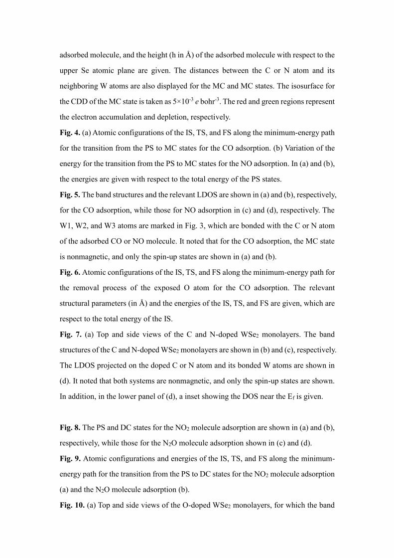
adsorbed molecule, and the height (h in Å) of the adsorbed molecule with respect to the
upper Se atomic plane are given. The distances between the C or N atom and its
neighboring W atoms are also displayed for the MC and MC states. The isosurface for
the CDD of the MC state is taken as 5×10⁻³ e bohr-3. The red and green regions represent
the electron accumulation and depletion, respectively.
Fig. 4. (a) Atomic configurations of the IS, TS, and FS along the minimum-energy path
for the transition from the PS to MC states for the CO adsorption. (b) Variation of the
energy for the transition from the PS to MC states for the NO adsorption. In (a) and (b),
the energies are given with respect to the total energy of the PS states.
Fig. 5. The band structures and the relevant LDOS are shown in (a) and (b), respectively,
for the CO adsorption, while those for NO adsorption in (c) and (d), respectively. The
W1, W2, and W3 atoms are marked in Fig. 3, which are bonded with the C or N atom
of the adsorbed CO or NO molecule. It noted that for the CO adsorption, the MC state
is nonmagnetic, and only the spin-up states are shown in (a) and (b).
Fig. 6. Atomic configurations of the IS, TS, and FS along the minimum-energy path for
the removal process of the exposed O atom for the CO adsorption. The relevant
structural parameters (in Å) and the energies of the IS, TS, and FS are given, which are
respect to the total energy of the IS.
Fig. 7. (a) Top and side views of the C and N-doped WSe2 monolayers. The band
structures of the C and N-doped WSe2 monolayers are shown in (b) and (c), respectively.
The LDOS projected on the doped C or N atom and its bonded W atoms are shown in
(d). It noted that both systems are nonmagnetic, and only the spin-up states are shown.
In addition, in the lower panel of (d), a inset showing the DOS near the Ef is given.
Fig. 8. The PS and DC states for the NO2 molecule adsorption are shown in (a) and (b),
respectively, while those for the N2O molecule adsorption shown in (c) and (d).
Fig. 9. Atomic configurations and energies of the IS, TS, and FS along the minimum-
energy path for the transition from the PS to DC states for the NO2 molecule adsorption
(a) and the N2O molecule adsorption (b).
Fig. 10. (a) Top and side views of the O-doped WSe2 monolayers, for which the band

structure is shown in (b). In (c), the LDOS are those projected on the doped O and its
bonded W atoms. The system is nonmagnetic, and only the spin-up states are shown.

VSe
3.07
2.52
Se W
VSe
(a)
Figure 1
-2
-1
0
1
2
Γ K M Γ
-50
0
50
-4 -3 -2 -1 0 1 2
-10
0
10
E (eV)
E (
eV
)
DO
S (
sta
tes
/eV
)
EfEf
TDOS
W 5d
(b) (c)
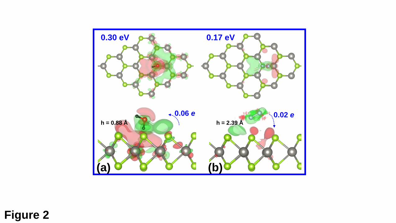
Figure 2
(a) (b)
0.30 eV 0.17 eV
h = 2.39 Åh = 0.88 Å
0.02 e0.06 e

Figure 3
1.14
2.13 2.03
2.24
1.28
2.042.13
2.02
1.68h = 2.23 h = -0.50 h = -0.76
0.23 eV 1.57 eV -1.03 eV
(a)
(b)
0.37 eV 3.15 eV 2.50 eV1.18 1.30
2.122.15
2.20
1.68
2.022.01
1.99
h = 1.30 h = -0.55 h = -0.76
PS MC DC MC
PS MC DC MC
W1
W2
W3
W1
W2
W3

-3
-2
-1
0
Figure 4
1.14
h = 2.23 h = -0.50
IS 0.00 eV FS -1.34 eV
(a)
TS 0.51 eV
1.15h = 0.85
1.28
(b)
E (
eV
)
PS
MC
-2
-1
0
1
2
0
1
2
0
2
0
2
-8 -6 -4 -2 0 20
2
-2
-1
0
1
2
Figure 5
Γ K M Γ
E (
eV
)
Ef
Ef
E (eV)
DO
S (
sta
tes/e
V)
W1 5d
W2 5d
W3 5d
O 2p
C 2p
E (
eV
)
Ef
-2
0
2
-2
0
2
-2
0
2
-8 -6 -4 -2 0 2
-2
0
2
DO
S (
sta
tes/e
V)
Ef
O 2p
N 2p
W1 5d
W2 5d
W3 5d
E (eV)Γ K M Γ
(a) (b) (c) (d)
2π* 2π*
2π*
2π*
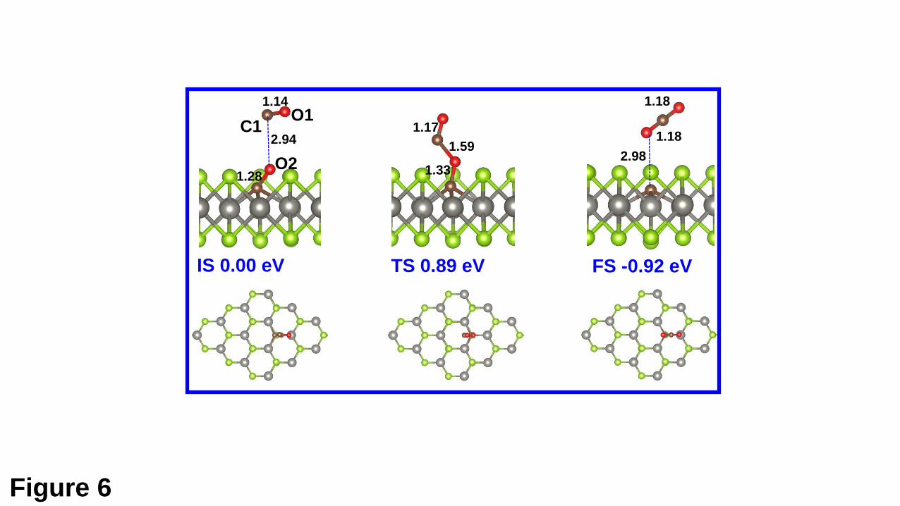
Figure 6
IS 0.00 eV FS -0.92 eVTS 0.89 eV
1.14
2.94
1.28
1.17
1.59
1.33
1.18
1.18
2.98
O1C1
O2
-2
-1
0
1
2
0
2
-8 -6 -4 -2 0 20
2
-2
-1
0
1
2
Figure 7
C
N
h = -0.81
2.01
2.03
h = -0.91
Ef
DO
S (
sta
tes/e
V)
E (eV)Γ K M Γ Γ K M Γ
E (
eV
)
W 5d
W2 5d
C 2p
W 5d
N 2p
Ef
Ef
(a) (b) (c) (d)
h = 2.08
0.24 eV 5.06 eV
h = -0.70
1.121.201.14
2.08
Figure 8
3.06
1.231.222.65
1.17h = 1.56 h = -0.70
2.08
0.36 eV 3.82 eV
(a) (b)
(c) (d)
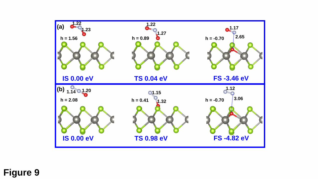
Figure 9
1.23
1.22
h = 1.56 2.65h = -0.70
1.171.27
1.22
IS 0.00 eV FS -3.46 eVTS 0.04 eV
h = 2.08
1.201.14
h = -0.70
1.12
3.061.32
1.15
h = 0.41
h = 0.89
IS 0.00 eV FS -4.82 eVTS 0.98 eV
(a)
(b)
-2
-1
0
1
2
Figure 10
h = -0.70
2.08
Γ K M Γ
E (
eV
) Ef 0
2
-8 -6 -4 -2 0 20
2
Ef
DO
S (
sta
tes/e
V)
E (eV)(a) (b) (c)
W 5d
O 2p