phonon and thermal properties of exfoliated tase2 thin films
TRANSCRIPT

1 | P a g e
Phonon and Thermal Properties of Exfoliated TaSe2 Thin Films
Z. Yan1, C. Jiang
1, T.R. Pope
2, C.F. Tsang
2, J.L. Stickney
2, P. Goli
3, J.
Renteria1, T.T. Salguero
2,* and A.A. Balandin
1,3,*
1Nano-Device Laboratory, Department of Electrical Engineering, Bourns College of Engineering,
University of California – Riverside, Riverside, California 92521 USA
2Department of Chemistry, University of Georgia, Athens, Georgia 30602 USA
3Materials Science and Engineering Program, Bourns College of Engineering, University of
California – Riverside, Riverside, California 92521 USA
Abstract
We report on the phonon and thermal properties of thin films of tantalum diselenide (2H-TaSe2)
obtained via the “graphene-like” mechanical exfoliation of crystals grown by chemical vapor
transport. The ratio of the intensities of the Raman peak from the Si substrate and the E2g peak of
TaSe2 presents a convenient metric for quantifying film thickness. The temperature coefficients
for two main Raman peaks, A1g and E2g, are -0.013 and -0.0097 cm-1
/oC, respectively. The
Raman optothermal measurements indicate that the room temperature thermal conductivity in
these films decreases from its bulk value of ~16 W/mK to ~9 W/mK in 45-nm thick films. The
measurement of electrical resistivity of the field-effect devices with TaSe2 channels indicates that
heat conduction is dominated by acoustic phonons in these van der Waals films. The scaling of
thermal conductivity with the film thickness suggests that the phonon scattering from the film
boundaries is substantial despite the sharp interfaces of the mechanically cleaved samples. These
results are important for understanding the thermal properties of thin films exfoliated from TaSe2
and other metal dichalcogenides, as well as for evaluating self-heating effects in devices made
from such materials.
KEYWORDS: van der Waals materials, tantalum diselenide, Raman spectroscopy, thermal
conductivity, metal dichalcogenide, thin film
*Corresponding authors: [email protected] (TTS) and [email protected] (AAB)

2 | P a g e
I. Introduction
The successful exfoliation of graphene [1] and discoveries of its unique electrical [2, 3] and
thermal [4-7] properties have motivated searches for other quasi two-dimensional materials with
interesting properties, as well as techniques for their synthesis and characterization [8-12]. As a
group, layered van der Waals materials [8] can be cleaved mechanically or exfoliated chemically
by breaking the relatively weak bonding between the layers. The resulting thin films can be re-
stacked into superlattice-type structures with various properties [8, 13, 14]. Some of us
previously have studied quintuples—five atomic layers—of bismuth telluride (Bi2Te3), which
reveal thermoelectric and topological insulator phenomena [13-16]. These quasi-2D crystals of
Bi2Te3 have electrical and thermal properties that are substantially different from those of bulk
Bi2Te3 [15, 16].
An interesting subgroup of inorganic van der Waals materials is the layered transition metal
dichalcogenides (MX2, where M=Mo, W, Nb, Ta or Ti and X=S, Se or Te) [17] Some of these
materials manifest charge density wave (CDW) effects in the temperature range from ~100 K to
room temperature [18]. In particular, we recently have found that decreasing the thickness of
titanium diselenide (TiSe2) thin films allows one to significantly increase the transition
temperature (TP) to the CDW phase [19]. This advance opens the possibility of CDW-based
devices that can operate near or at room temperature.
In this paper we report on the physical properties of TaSe2 films prepared by “graphene-like”
mechanical exfoliation. We focus on their phonon and thermal properties, which are essential for
the metrology of such films and for possible device applications. Indeed, apart from graphene
and hexagonal boron nitride, layered van der Waals materials typically have rather low values of
thermal conductivity, K [6, 13, 14]. Thin films of such materials should have even lower K
values due to phonon–boundary scattering. However, because the thermal conductivity in such
materials is strongly anisotropic (substantially larger in-plane) and the cleaved surfaces can be
rather smooth, the change in K due to film thinning is difficult to predict. The degraded thermal
conductivity can become a major impediment for practical applications due to unavoidable
power dissipation and self-heating effects. The contribution of electrons to thermal transport in
thin films of metal dichalcogenides is also not known precisely. Thus the main goals of this
study are to characterize the phonon spectrum, the relative contributions of phonons and

3 | P a g e
electrons to heat conduction and the extent of thermal conductivity degradation in TaSe2 thin
films.
The crystal structure of TaSe2 consists of Se-Ta-Se layers containing Ta in trigonal prismatic
coordination. The weak interlayer van der Waals bonding permits the facile mechanical
delamination and exfoliation of such crystals, and it also leads to several TaSe2 polytypes that
differ in the relative orientation of the layers and their stacking arrangements. In this work, we
specifically examine 2H-TaSe2. The structure of this polytype has a two-layer repeat pattern
(AcA BcB), within which the trigonal prismatic units are rotated 60o with respect to each other
[20-22].
II. Material Synthesis and Sample Preparation
The 2H-TaSe2 crystals used in this study were derived from 3R-TaSe2 powder according to
standard methods [21]. Briefly, we first prepared TaSe2 from the elements. After two firing
cycles at 700 and 900 °C, the product consisted of mostly 3R-TaSe2 with traces of the 2H-TaSe2
form, which is typical for this synthetic route [21, 23]. Then this material was heated in the
presence of I2 within a sealed ampule with a 100 °C temperature gradient; these “chemical vapor
transport” conditions [24] resulted in clusters of metallic gray crystals. As shown in Figure 1 (a,
b, and d inset), these crystals have lateral dimensions of approximately 200-800 m and
thicknesses of approximately 5 to 30 m. Powder X-ray diffraction (XRD) reveals that the major
phase of crystallized material is the 2H-TaSe2 polytype; as shown in Figure 1c, the experimental
diffraction pattern matches literature data for 2H-TaSe2 very well [25, 26]. In addition, we
observe traces of 3R-TaSe2, in line with common observations of polytype mixtures within Ta-
Se systems [20, 23]. The presence of this minor component does not affect subsequent samples
that are derived from the mechanical delamination of 2H-TaSe2 single crystals.
Both energy-dispersive X-ray spectroscopy (EDS) and electron probe microanalysis (EPMA)
data confirm that the composition of the crystals is within a few percent of the ideal
stoichiometry (Figure 2 (d) and Table I). Several factors that may contribute to the observed
variation include: (i) EPMA data were collected from a non-ideal crystal surface, which
introduces additional error, (ii) incorporation of oxide impurities, and/or (iii) possible non-

4 | P a g e
stoichiometry, which is known in the range of x<0.03 and 0.25<x<0.64 for 2H-Ta1+xSe2 [21, 23,
27]. In particular, X-ray photoelectron spectroscopy (XPS) indicates that the TaSe2 crystal
surfaces become oxidized upon exposure to air. Figures 1 (e) and (f) show XPS data for the Ta 4f
and Se 3d photoelectric peaks from a series of samples. By comparison with a reference sample
of Ta foil that exhibits both Ta metal and its native oxide Ta2O5 [28], we can see that 2H-TaSe2
crystals also contain Ta oxide [29]. However, upon mechanical delamination of surface layers
from the 2H-TaSe2 crystals, the only remaining visible species is TaSe2.
Thin films of 2H-TaSe2 were prepared on Si/SiO2 substrates following the standard “graphene-
like” approach [1-3]. The thickness H of the films ranged from a few trilayers to H=300 nm. The
Se-Ta-Se atomic trilayer has a thickness c=6.359 Å and the lattice parameter a=3.434Å (see
Figure 2). The crystal structure of 2H-TaSe2 belongs to the space group D6h4 and it has a unit cell
consisting of two Se-Ta-Se trilayers. We used Raman spectroscopy as a metrology tool to verify
the quality of the crystals and determine the thicknesses of the flakes. Raman spectroscopy
(Renishaw InVia) was performed in the backscattering configuration under λ = 633 nm laser
excitation. An optical microscope (Leica) with a 50× objective was used to collect the scattered
light. To avoid possible self-heating effects, the excitation laser power for Raman spectroscopic
measurements was kept low at P<0.5 mW (on the sample surface).
III. Raman Metrology of van der Waals Thin Films
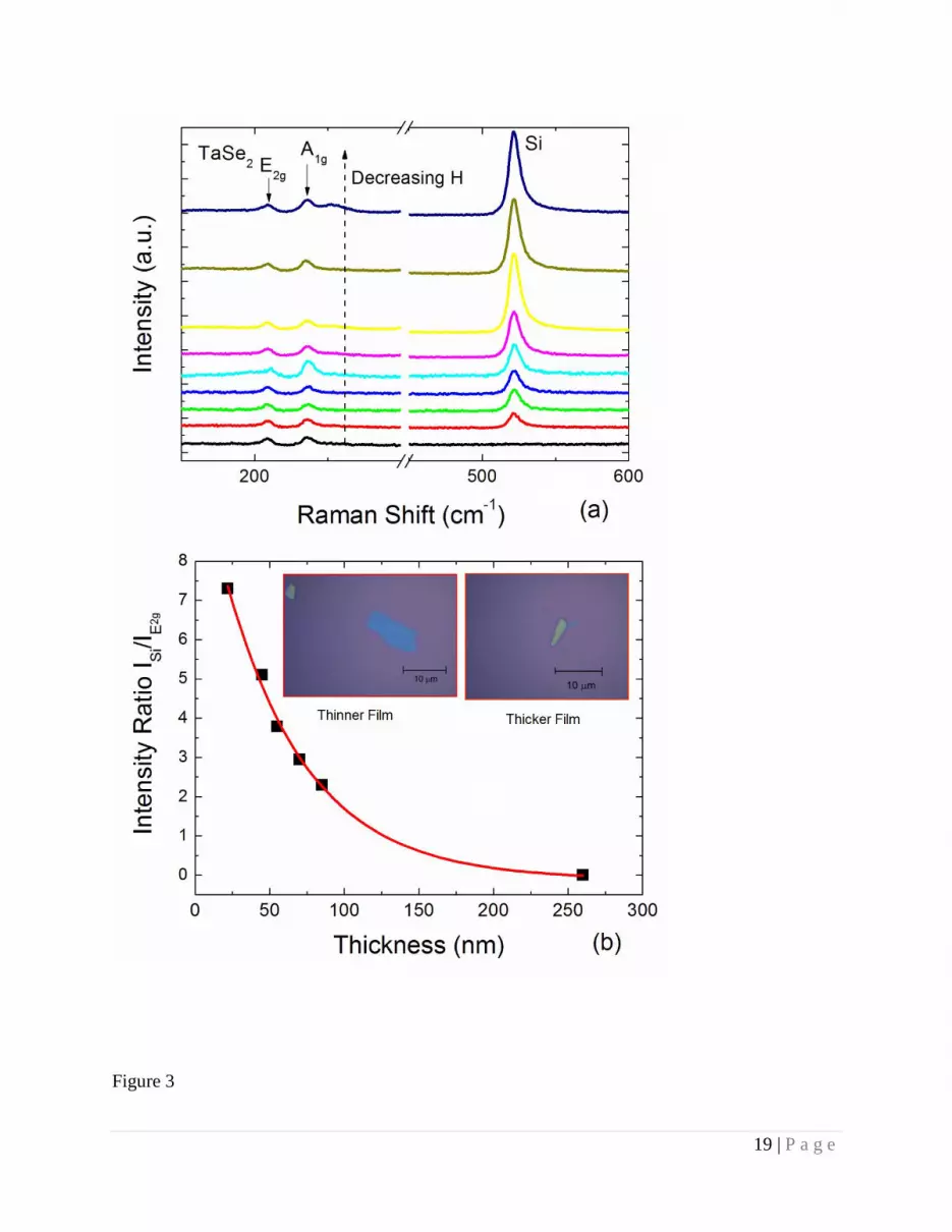
Figure 3 (a) shows Raman spectra of TaSe2 for nine exfoliated thin films with different
thicknesses H ranging from a few nm to >250 nm. The thicknesses of the exfoliated films were
measured by atomic force microscopy (AFM). The 2H-TaSe2 crystal possesses 12 zone center
lattice vibrational modes. Four of these modes (E2
2g , E1g , E12g and A1g) are Raman active. The
atomic displacements for these vibrational modes are shown in Figure 3 (b). The A1g and E1
2g
modes can be clearly seen in the Raman spectra at ~235 cm-1
and ~207 cm-1
, respectively (see
Figure 3 (a)). The modes with the energy lower than 130 cm-1
are blocked by the Rayleigh filter
of the spectrometer. There have been few reports of Raman data for TaSe2 [30-33]. In contrast,
earlier studies used bulk TaSe2 samples and focused on the lower frequency portion of the
spectrum [30-32]. Comparison of our data with that in Ref. [33] indicates that the peak positions
and mode assignments are consistent.

5 | P a g e
The pronounced Si peak from the substrate appears at 522 cm-1
. The intensity of the Brillouin
zone-center Si peak is proportional to the interaction volume. It explains why the peak intensity
is increasing with decreasing thickness of TaSe2 film placed on top of Si substrate. The ratio of
the intensity of Si peak to that of A1g or E2g can be used for determining the thickness of the
exfoliated film. Figure 3 (b) presents the ratio of the intensity of the Si peak to that of the E2g
peak, I(Si)/I(E2g), as a function of thickness H. This ratio decreases exponentially with increasing
film thickness and can be fitted with the equation 11.0)9.54/exp(2.11)(/)( 2 HEISiI g
(here the thickness H is in the units of nm). The obtained dependence can be used as a calibration
curve for the Raman-based nanometrology of TaSe2 films. The approach can be extended to
other layered van der Waals materials. From a practical perspective, the Raman metrology of
exfoliated films is easier and faster than AFM inspection.
The temperature dependence of Raman spectra of 2H-TaSe2 were studied in the temperature
range from 83 K to 613 K. The sample with exfoliated TaSe2 flake was put in a cold-hot cell and
the temperature can be controlled externally with 0.1 oC accuracy. Figure 4 (a) shows the Raman
spectrum of a typical TaSe2 flake measured at different temperatures. The Raman peak positions
of both A1g and E12g modes move to lower wavenumber range (red shift) when temperature
increases. The Raman peak positions of TaSe2 A1g and E1
2g modes at the different temperatures
are shown in Figure 4 (b). In the measured temperature range, the temperature dependence of A1g
and E1
2g modes can be represented by a linear relation T 0 , where 0 is the frequency
of Raman peak when temperature T is extrapolated to 0 K, and is the first-order temperature
coefficient. The extracted temperature coefficients of A1g mode and E1
2g mode are 013.01
cm-1
/oC and 0097.02 cm
-1/oC, respectively. The softening of A1g and E2g modes with
increasing temperature is in agreement with the report for bulk 2H-TaSe2 [30]. However, a direct
quantitative comparison of the temperature coefficients is not possible because our data are for
thin films rather than bulk and for a different temperature range.
IV. Thermal Properties of TaSe2 Thin Films

6 | P a g e
The obtained temperature coefficients characterize the inharmonicity of the TaSe2 crystal lattice.
They also can be used to extract the thermal conductivity data using the Raman optothermal
technique, which was originally developed for graphene [5]. The data presented in Figure 4 (b)
can be used as calibration curves for determining the local temperature rise in TaSe2 flakes. The
temperature is extracted from the shift of Raman peak positions. In a sense, the Raman
spectrometer is thus used a thermometer. For the thermal measurements, we intentionally
increase the intensity of the excitation laser so that it induces a local heating of the sample. The
low thermal conductivity of TaSe2 allows one to achieve local heating at the power level of about
1-2 mW. Figure 5 (a) shows a characteristic Raman mode of the tested TaSe2 flake at low and
high excitation power. The Raman peak position of E2g peak shifts from 209.1 cm-1
to 207.7 cm-1
as the power increase by 90%. The calculated change in the local temperature introduced by laser
is ~ 144 o
C. The measurements were repeated using another Raman peak of TaSe2 to ensure
reproducibility of the local temperature measurement.
The temperature rise for a known dissipated power and sample geometry allow one to determine
the thermal conductivity [5]. We have used the finite element method (FEM) to simulate the heat
dissipation in the samples under test. The thermal conductivity was determined via the iteration
approach. For the first simulation run, the thermal conductivity of TaSe2 flake was assumed to
have the value of K0. The numerical simulation with the assumed value of thermal conductivity
resulted in the modeled temperature rise ΔT0. The simulated temperature rise was compared with
the experimental temperature rise ΔT. If ΔT0 was larger (smaller) than ΔT, the assumed value of
the thermal conductivity K was increased (decreased) in the next run until the simulated
temperature rise matched the experimental data and the final value of K was obtained. This
procedure also requires the knowledge of the power dissipated in the thin film. The power level
at the sample surface is measured directly with a detector. The absorption coefficient in the thin
film can be deduced from the ratio of the integrated Raman intensity of Si peak from the
substrate with TaSe2 films placed on top of it to the Si peak of the substrate not covered with the
TaSe2 peak (see Figure 5 (b)). One can see that this ratio decreases when the film thickness
increases and goes all the way to zero, which means that all laser power is absorbed in the film.
The film thickness dependence of the Si peak intensity ratio can be fitted by an exponential
decay function 04.0)1.27/exp(06.1/)( 0 HIHI SiSi , where H is the film thickness in unit of

7 | P a g e
nm, and the extracted absorption coefficient, α , is 27.1 nm-1
.The details of the FEM based
procedure for extraction of thermal conductivity have been described in Ref. [34].
The inset to Figure 5 (b) presents a schematic of the simulated sample structure. The radius of
simulated domain size is 100 μm and the radius of TaSe2 flake and the laser spot are 4 µm and
0.5 μm, respectively. The thicknesses of TaSe2 flakes used for extraction of thermal conductivity
were H=45 nm, H=55 nm and H= 85 nm. The thickness of the silicon dioxide layer and silicon
substrate were 300 nm and 0.5 mm, respectively. The silicon substrate was placed on an ideal
heat sink so that the temperature at the bottom side was fixed at 300 K. The adiabatic conditions
were assumed at other external boundaries. For the TaSe2 flake with H=45 nm we obtained the
experimental shift in the Raman peak position =-1.4 cm-1
as the power on the sample surface
changed from 0.11 mW to 1.15 mW. This corresponds to a local temperature rise of T=144 K.
The software-enhanced resolution of the micro-Raman spectrometer in these measurements was
estimated to be 0.1 cm-1
, which sets the experimental error at about 10%. Errors related to
radiative losses were estimated to be less than 10% due to the relatively fast time scale of the
measurements. The results of the measurements are summarized in Table II. One can see that the
room temperature thermal conductivity in these films decreases from its bulk value of about 16
W/mK to ~9 W/mK in 45-nm thick films. Although the electrical and thermal transport
properties of graphite intercalation compounds and MX2 materials were studied even earlier than
mechanically exfoliated graphene [35-36], only a few prior reports have addressed the thermal
properties of TaSe2 and related materials [37-39]. It has been reported that the room temperature
thermal conductivity of bulk 2H-TaSe2 is ~16 W/mK [39]. Our results for mechanically
exfoliated thin films are consistent with the prior measurements for bulk 2H-TaSe2 [37-39].
For practical applications, it is important to understand whether the heat conduction is dominated
by the phonon or electron contributions. To determine this distinction, we fabricated four-
terminal devices with the channels implemented with thin film 2H-TaSe2. We used electron
beam lithography to define the top metal contacts for the electrical measurements. The top
contacts were fabricated with 10 nm of Ti and 100 nm of Au. Figure 6 shows the current-voltage
(I-V) characteristics of a representative device. The insets show the optical microscopy image of
the 2H-TaSe2 device and the linear region used for extraction of the electrical conductivity .

8 | P a g e
The channel lengths, widths and thicknesses were 9 m, 6.5 m and 80 nm, respectively. The
experimentally determined conductivity of the 2H-TaSe2 channel was =0.365 1/m for this
device. Using the Wiedemann–Franz law, K/T=(2/3)(kB/e)
2, we estimated that the contribution
of electrons to thermal conductivity of thin films of intrinsic 2H-TaSe2 is ~3x10⁻⁶
W/mK. This
means that the heat conduction is dominated by phonons.
Our data indicate that the thermal conductivity starts to decrease when the film thickness
becomes comparable to the phonon mean free path in the material. The latter suggests that the
observed decrease of the thermal conductivity, as compared to bulk value, is related to the
acoustic phonon–boundary scattering. This is a non-trivial conclusion because one may have
expected that in exfoliated thin films of van der Waals materials the smooth interfaces of the
cleaved films will lead to negligible phonon – boundary scattering. It also is known that the
thermal conductivity in MX2 materials is strongly anisotropic (much larger in-plane K) and thus
variations of thickness may not necessarily produce strong effects. Our results indicate that the
thermal transport in exfoliated films on substrates is dominated by extrinsic effects, such as
boundary scattering, rather than by the intrinsic lattice dynamic properties of van der Waals films.
V. Conclusions
We investigated the phonon and thermal properties of 2H-TaSe2 thin films prepared by the
mechanical delamination of crystals. We have established that the intensities of Raman peaks
from the films and the Si substrate can be used for the robust and fast nanometrology of TaSe2
thin films. The Raman nanometrology method can be readily extended to other layered van der
Waals materials. We also found that the thermal conductivity of the exfoliated thin films of 2H-
TaSe2 is dominated by the phonon contributions and reduced substantially compared to the bulk
value. The Raman optothermal measurements indicate that the room temperature thermal
conductivity in these films decreases from its bulk value of ~16 W/mK to ~9 W/mK in 45-nm
thick films. These results suggest that thermal issues need to be taken into account in proposed
device applications of TaSe2, other metal dichalcogenide and van der Waals materials.

9 | P a g e
METHODS
Material Growth and Experimental Techniques: For the TaSe2 crystal growth, the elements
were used as received: tantalum (99.9% trace metal basis) from Sigma-Aldrich Corp., selenium
(99.99%) from Strem Chemicals Inc., iodine (99.9%) from J.T. Baker. For SEM and EDS, the
samples were prepared by sprinkling crystals onto double-sided carbon tape. The images were
acquired with an FEI Inspect F field emission gun scanning electron microscope operated at 20
keV. EDS data were collected with an EDAX Inc. instrument at 20 KeV for 19.7 s. For XRD, the
samples were prepared by grinding the material with an agate mortar/pestle and then pressing
into an aluminum mount. The patterns were acquired using a Bruker D8-Advance diffractometer
(Co-Kα radiation source) operated at 40 mA and 40 kV. Data were collected from 2-80 2θ at a
rate of 0.1 s per step. For EPMA, the samples were prepared by placing crystals flat on double-
sided carbon tape. The data were acquired on the crystal surfaces parallel to the substrate using a
JEOL JXA 8600 Superprobe. XPS analyses were performed using a Mg K1,2 (STAIB) source
and a hemispherical analyzer from Leybold Heraeus; the take-off angle was about 40°. The
preparation of TaSe2 followed the following steps. The stoichiometric amounts of elemental Ta
and Se were sealed in a well-evacuated quartz ampule (backfilled 3x with high purity Ar). This
mixture was heated at 700 °C for 15 hours, cooled to room temperature, and then thoroughly
mixed by shaking. This material was heated again at 900 °C for an additional 15 hours. The final
product was a black, glittery, free-flowing powder. The chemical vapor transport of TaSe2 used
the following procedures. The previously synthesized 3R-TaSe2 was loaded into a quartz ampule
with 3 mg cm–3
of I2. The ampule was evacuated (while immersed in a dry ice/acetone bath) and
sealed, then heated with a ramp of 1 °C min–1
in a tube furnace until a gradient of 730 to 830 °C
(from the cool end to the hot end of the ampule) was achieved. Those temperatures were held for
one week, then the sample was cooled to room temperature at 1 °C min–1
. After removal from
the ampule, the metallic grey crystals were warmed slightly under vacuum to remove any traces
of I2.
Numerical Modeling Approach for Thermal Data: The modeling of heat diffusion in TaSe2
thin films on Si substrate was performed using the finite element method implemented in
COMSOL software package with the Heat Transfer Module. The schematic of the simulated

10 | P a g e
sample structure is presented in the inset to Figure 5 (b). The substrate consists of 0.5 mm Si and
300 nm SiO2 layer. The radius of the Si/SiO2 used in the simulated domain is 100 µm. The
thickness and radius of TaSe2 layer varied for different flakes according to the values obtained
experimentally. The radius of laser spot size is 0.5 µm. The heat conduction was simulated by
solving numerically Fourier's law QTK )( , where K is the thermal conductivity, T is the
absolute temperature and Q is the power density of the heat source. The thermal conductivity
values of Si and SiO2 used in the simulation were 140 W/mK and 1.4 W/mK, respectively. The
absorbed laser power density along z direction can be described by the following function
)exp()( 0 zQzQ , where Q0 is the laser power density at the top surface of the sample, α
is the absorption coefficient of TaSe2 film obtained in previous steps. For a given dissipation
power and sample geometry, the numerical modeling generates a temperature profile in the
sample structure. Due to the axial symmetry of the simulation domain around z direction, the
temperature profile in the whole sample structure can be fully represented by the simulation
results in z- cross-section, where r is coordinate in the cylindrical coordinate system. The
thermal conductivity of thin films of TaSe2 films was determined via the iteration approach as
described in Ref. [34].
Acknowledgements
This work was funded, in part, by the National Science Foundation (NSF) and Semiconductor
Research Corporation (SRC) Nanoelectronic Research Initiative (NRI) project 2204.001:
Charge-Density-Wave Computational Fabric: New State Variables and Alternative Material
Implementation (NSF-1124733) as a part of the Nanoelectronics for 2020 and beyond (NEB-
2020) program. AAB also acknowledges particle support from the STARnet Center for Function
Accelerated nanoMaterial Engineering (FAME) – SRC program sponsored by MARCO and
DARPA.

11 | P a g e
References
[1] Novoselov, K. S.; Geim, A. K.; Morozov, S. V.; Jiang, D.; Zhang, Y.; Dubonos, S. V.;
Grigorieva, I. V.; Firsov, A. A. Science 2004, 306, 666-9.
[2] Novoselov, K. S.; Geim, A. K.; Morozov, S. V.; Jiang, D.; Katsnelson, M. I.; Grigorieva,
I. V.; Dubonos, S. V.; Firsov, A. A. Nature 2005, 438, 197-200.
[3] Zhang, Y.; Tan, Y.-W.; Stormer, H. L.; Kim, P. Nature 2005, 438, 201-204.
[4] Balandin, A. A.; Ghosh, S.; Bao, W.; Calizo, I.; Teweldebrhan, D.; Miao, F.; Lau, C. N.
Nano Letters 2008, 8, 902-907.
[5] Ghosh, S.; Bao, W.; Nika, D. L.; Subrina, S.; Pokatilov, E. P.; Lau, C. N.; Balandin, A. A.
Nat Mater 2010, 9, 555-558.
[6] Balandin, A. A. Nat Mater 2011, 10, 569-581.
[7] Nika, D. L.; Balandin, A. A. Journal of Physics.: Condensed Matter: 2012, 24, 233203.
[8] Geim, A. K.; Grigorieva, I. V. Nature 2013, 499, 419-425.
[9] Teweldebrhan, D.; Goyal, V.; Balandin, A. A. Nano Letters 2010, 10, 1209-1218.
[10] Mas-Balleste, R.; Gomez-Navarro, C.; Gomez-Herrero, J.; Zamora, F. Nanoscale 2011, 3,
20-30.
[11] Koski, K. J.; Cui, Y. ACS Nano 2013, 7, 3739-3743.
[12] Xu, M.; Liang, T.; Shi, M.; Chen, H. Chemical Reviews 2013, 113, 3766-3798.
[13] Goyal, V.; Subrina, S.; Nika, D. L.; Balandin, A. A. Applied Physics Letters 2010, 97,
031904.
[14] Shahil, K. M. F.; Hossain, M. Z.; Teweldebrhan, D.; Balandin, A. A. Applied Physics
Letters 2010, 96, 153103.
[15] Hossain, M. Z.; Rumyantsev, S. L.; Shahil, K. M. F.; Teweldebrhan, D.; Shur, M.;
Balandin, A. A. ACS Nano 2011, 5, 2657-2663.
[16] Khan, J.; Nolen, C. M.; Teweldebrhan, D.; Wickramaratne, D.; Lake, R. K.; Balandin, A.
A. Applied Physics Letters 2012, 100, 043109.
[17] Chhowalla, M.; Shin, H. S.; Eda, G.; Li, L.-J.; Loh, K. P.; Zhang, H. Nat Chem 2013, 5,
263-275.
[18] Grüner, G. Reviews of Modern Physics 1988, 60, 1129-1181.
[19] Goli, P.; Khan, J.; Wickramaratne, D.; Lake, R. K.; Balandin, A. A. Nano Letters 2012,
12, 5941-5945.

12 | P a g e
[20] Brown, B. E.; Beerntsen, D. J. Acta Crystallographica 1965, 18, 31-36.
[21] Preparation and Crystal Growth of Materials with Layered Structures. R. M. A. Lieth
(Ed.), Physics and Chemistry of Materials with Layered Structures, Vol. 1, D. Reidel Publishing
Company: Dordrecht, Holland, 1977
[22] Wilson, J. A.; Yoffe, A. D. Advances in Physics 1969, 18, 193-335.
[23] Selte, K.; Bjerkelund, E.; Kjekshus, A. Journal of the Less Common Metals 1966, 11, 14-
30.
[24] Binnewies, M.; Glaum, R.; Schmidt, M.; Schmidt, P. Zeitschrift für anorganische und
allgemeine Chemie 2013, 639, 219-229.
[25] Li, L. J.; Sun, Y. P.; Zhu, X. D.; Wang, B. S.; Zhu, X. B.; Yang, Z. R.; Song, W. H. Solid
State Communications 2010, 150, 2248-2252.
[26] Bjerkelund, E.; Kjekshus, A. Acta Chem. Scand. 1967, 21, 513-526.
[27] Huisman, R.; Kadijk, F.; Jellinek, F. Journal of the Less Common Metals 1970, 21, 187-
193.
[28] Wang, K.; Liu, Z.; Cruz, T. H.; Salmeron, M.; Liang, H. The Journal of Physical
Chemistry A 2010, 114, 2489-2497.
[29] Waldvogel, H. P.; Schärli, M. Journal of Electron Spectroscopy and Related Phenomena
1984, 34, 115-128.
[30] Steigmeier, E. F.; Harbeke, G.; Auderset, H.; DiSalvo, F. J. Solid State Communications
1976, 20, 667-671.
[31] Holy, J. A.; Klein, M. V.; McMillan, W. L.; Meyer, S. F. Physical Review Letters 1976,
37, 1145-1148.
[32] Li, H.; Lu, G.; Wang, Y.; Yin, Z.; Cong, C.; He, Q.; Wang, L.; Ding, F.; Yu, T.; Zhang,
H. Small 2013, 9, 1974-1981.
[33] Castellanos-Gomez, A.; Navarro-Moratalla, E.; Mokry, G.; Quereda, J.; Pinilla-
Cienfuegos, E.; Agraït, N.; Zant, H. J.; Coronado, E.; Steele, G.; Rubio-Bollinger, G. Nano
Research 2013, 6, 191-199.
[34] Chen, S.; Wu, Q.; Mishra, C.; Kang, J.; Zhang, H.; Cho, K.; Cai, W.; Balandin, A. A.;
Ruoff, R. S. Nat Mater 2012, 11, 203-207.
[35] M.S. Dresselhaus a & G. Dresselhaus, Advances in Physics 1981, 30, 139-326.

13 | P a g e
[36] J.-P. Issi, Transport Properties of Metal Chloride Acceptor Graphite Intercalation
Compounds, in Springer Series in Materials Science, vol. 18, 195 (1992).
[37] Brixner, L. H.; Teufer, G. Inorganic Chemistry 1963, 2, 992-996.
[38] Harper, J. M. E.; Geballe, T. H.; DiSalvo, F. J. Physical Review B 1977, 15, 2943-2951.
[39] Núñez-Regueiro, M. D.; Lopez-Castillo, J. M.; Ayache, C. Physical Review Letters 1985,
55, 1931-1934.

14 | P a g e
Table I: Comparison of EDS and EPMA data from 2H-TaSe2 crystals
Theoretical
Weight %
Experimental
Weight %
Theoretical
Atomic %
Experimental
Atomic %
EPMA EDS EPMA EDS
Se 46.60 47.60 43.23 66.00 67.80 63.57
Ta 53.40 51.86 56.77 33.00 32.24 36.43
Total
Weight %
100.0 99.46 100.0 --- --- ---
Se/Ta --- --- --- 2.00 2.10 1.74
Table II: Thermal conductivity of exfoliated 2H-TaSe2 thin films at room temperature
Thickness H (nm) 45 55 85 Bulk
K (W/mK) 9 11 16 16

15 | P a g e
FIGURE CAPTIONS
Figure 1: Characterization of 2H-TaSe2 crystals grown by the chemical vapor transport method:
(a) Optical microscopy image (scale bar is 250 m). (b) Scanning electron microscopy (SEM)
image (scale bar is 30 m). (c) Powder X-ray diffraction data. The top red trace shows the
pattern from as-grown TaSe2 crystals; the primary component is 2H-TaSe2 (database comparison
shown at bottom) with traces of 3R-TaSe2 (marked with *). (d) Energy dispersive X-ray
spectroscopy data for a 2H-TaSe2 crystal (SEM inset, scale bar is 100 m). (e) X-ray
photoelectron spectroscopy (XPS) spectra showing the Ta 4f photoelectric peaks from 2H-TaSe2
crystals before (red curve) and after (blue curve) peel-off of surface layers. The spectrum of
Ta2O5 on Ta foil (black curve) is included for reference. (f) XPS spectra showing the Se 3d
photoelectric peaks from 2H-TaSe2 crystals before (red curve) and after (blue curve) peel-off of
surface layers.
Figure 2: Crystal structure of 2H-TaSe2 (a) and schematic of its main vibrational modes.
Figure 3: (a) Raman spectrum of the exfoliated thin films of TaSe2 on Si substrate. The data is
shown for the films thickness ranging from ~260 nm to below 30 nm. The characteristics E2g and
A1g peaks of TaSe2 are clearly observed. The intensity of Si peak at 522 cm-1
is increasing with
the decreasing thickness of TaSe2 film. (b) The ratio of the intensity of Si peak to E2g peak in
Raman spectrum of TaSe2. The calibrated intensity ratio can be used for nanometrology of TaSe2
films. The insets show optical microscopy images of two flakes of TaSe2 with substantially
different thickness. The thinner flakes appear blue in color whereas the thicker flakes appear
yellow.
Figure 4: (a) Evolution of Raman spectrum of 2H-TaSe2 thin film with temperature. A new peak
appears in the spectra at about 250 cm-1
after temperature decreases below ~220 K. The peaks
shift their position with temperature. (b) Temperature coefficients 1 and 2 for E2g and A1g
Raman peaks of 2H-TaSe2, respectively. The temperature coefficients can be used for the
extraction of the thermal conductivity of thin films using the Raman optothermal method.
Figure 5: (a) Shift and broadening of the Raman peaks of 2H-TaSe2 as a result of local heating
with the excitation laser. (b) Intensity ratio of the Si Raman peak from the substrate without thin

16 | P a g e
film to that of the substrate covered with 2H-TaSe2 thin film. The data allows one to estimate the
amount of power absorbed by the film. The inset shows a model used for extraction of the
thermal conductivity of thin films of 2H-TaSe2.
Figure 6: Current-voltage characteristic of a two-terminal device with 2H-TaSe2 channel. The
upper inset show optical microscopy image of the device. The lower inset shows the small-bias
region of I-V curve used for determining the resistivity of the exfoliated flake of 2H-TaSe2.

17 | P a g e
Figure 1

18 | P a g e
Figure 2
19 | P a g e
Figure 3

20 | P a g e
Figure 4

21 | P a g e
Figure 5

22 | P a g e
Figure 6