performance caches helen h. ruan - citeseerx
TRANSCRIPT
Analysis and Design Considerations for High
Performance Caches
by
Helen H. Ruan
Submitted to the Department of Electrical Engineering andComputer Science in Partial Fulfillment of the
Requirements for the Degrees of Bachelor of Science inElectrical Engineering and Master of Engineering in
Electrical Engineering and Computer Science
at the
MASSACHUSETTS INSTITUTE OF TECHNOLOGY
January 1998
© Helen H. Ruan All Rights Reserved.
The author hereby grants to M.I.T. permission to reproduceand distribute publicly paper and electronic copies of this
thesis.
Author ......... /. .......................Department of Electrical Engineering and Computer Science
A/ January 23, 1998
Certified by ........................................Tho as F. Knight JR
Sesis Supervisor
Accepted by ..... . .........................Arthur C. Smith
Chairman, Department Committee on Graduate Theses
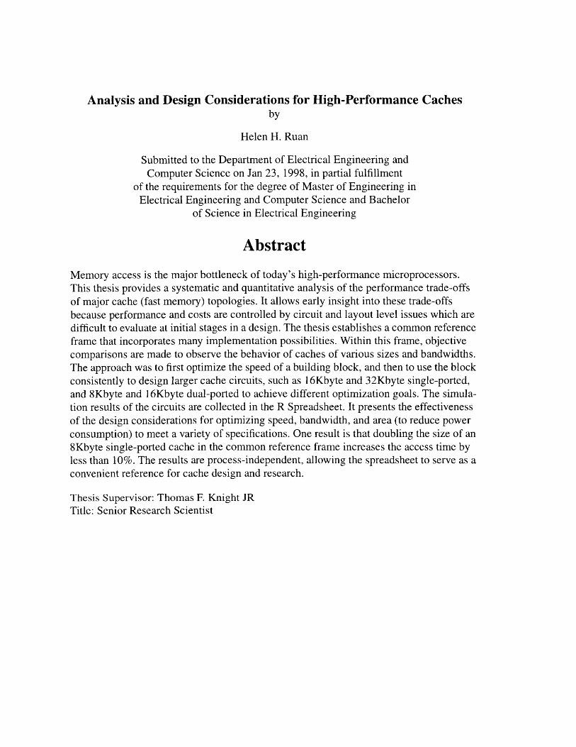
Analysis and Design Considerations for High-Performance Cachesby
Helen H. Ruan
Submitted to the Department of Electrical Engineering andComputer Science on Jan 23, 1998, in partial fulfillment
of the requirements for the degree of Master of Engineering inElectrical Engineering and Computer Science and Bachelor
of Science in Electrical Engineering
Abstract
Memory access is the major bottleneck of today's high-performance microprocessors.This thesis provides a systematic and quantitative analysis of the performance trade-offsof major cache (fast memory) topologies. It allows early insight into these trade-offsbecause performance and costs are controlled by circuit and layout level issues which aredifficult to evaluate at initial stages in a design. The thesis establishes a common referenceframe that incorporates many implementation possibilities. Within this frame, objectivecomparisons are made to observe the behavior of caches of various sizes and bandwidths.The approach was to first optimize the speed of a building block, and then to use the blockconsistently to design larger cache circuits, such as 16Kbyte and 32Kbyte single-ported,and 8Kbyte and 16Kbyte dual-ported to achieve different optimization goals. The simula-tion results of the circuits are collected in the R Spreadsheet. It presents the effectivenessof the design considerations for optimizing speed, bandwidth, and area (to reduce powerconsumption) to meet a variety of specifications. One result is that doubling the size of an8Kbyte single-ported cache in the common reference frame increases the access time byless than 10%. The results are process-independent, allowing the spreadsheet to serve as aconvenient reference for cache design and research.
Thesis Supervisor: Thomas F. Knight JRTitle: Senior Research Scientist

Acknowledgments
This thesis would not have been possible without the support of many people. The fol-lowing individuals and organizations have been most generous with their support through-out my thesis work period.
* First, I would like to express my gratitude to Intel Corporation for selecting me as astudent of the MIT-Intel Cooperative Program and for giving me the opportunity towork on the foremost microprocessor core designs. My co-op experiences at the com-pany helped me tremendously by giving me a head start in choosing and learningabout the technical areas I needed to understand for my thesis.
* I would like to thank Intel's MRL (Microprocessor Research Labs) and the micropro-cessor core design group in Oregon for providing me with the opportunity to doresearch and the design facility I needed to implement the work for this thesis. Cachedesign and circuit design experts at Intel gave me extremely valuable technical supportwhile I was working on my third co-op assignment.
* I would also like to thank my thesis advisor Thomas Knight for pinpointing key techni-cal issues. His comments have helped widen my perspectives. My co-op advisor Jesusdel Alamo, who serves as the liaison between MIT and Intel, also supported me bymaking sure that my thesis work progressed smoothly at Intel and MIT. I thank mytechnical mentor David Harris too for all his encouragement and help.
* Most importantly, I would like to thank my loving family: my parents and my brother.They have always been there for me. The curiosity about science and high-tech hasalways been in my blood because of my parents. They encourage and inspire me all thetime. I would like to dedicate this thesis to them.
Table of Contents
C hapter 1 Introduction .................. ... ........ .. .. ................. ... .................................... 6
Chapter 2 Existing Work on Cache Modeling ...................................... .............. 10
C hapter 3 H igh-Level Issues....................................................................................... 12
3.1 Partitioning Cache Wordline and Bitline Length........................................... 13
3.2 Determining Degree of Associativity ...................................... ....... 14
3.3 Major Assumptions Made......................... .......................... 14
3.3.1 Data Array Access is Critical................. .................. 14
3.3.2 Begin and End of Access Time................................ 15
3.3.3 Virtually Indexed, Physically Tagged Arrays............................... 16
3.3.4 Way Prediction......................................... 17
3.3.5 Control Signals ...................... . ...................... 17
3.3.6 Neighboring FUBs ........................... .... ................. 18
Chapter 4 Implementation Details and Circuits................. ................. 19
4.1 Introduce an Optimized Building Block ......................................................... 19
4.2 Circuit Topology and Specific Component Design ..................................... 21
4.2.1 Predecoder.......................... .............................. 21
4 .2 .2 D ecoder .................................................... ..................... ....................... 22
4.2.3 W ordline Loads.......................................................... 22
4.2.4 B it C ells ......................................................................................... 23
4.2.5 Bitline Loads ................................................. 23
4.2.6 Precharge, Write Buffer, and Read Mux ...................................... 23
4.2.7 Sense Amplifier Precharge and Sense Amplifier............................ 24
4.2.8 Output Loads Modeling ....................... ................... 24
4.3 Timing Requirements............................ . . .... ....................... 25
4.4 Building Abstractions .......................................................... 26
4.4.1 16kB Single-Ported Caches .................................. 26
4.4.2 32kB Single-Ported Caches ......................... .. ............... 29
4.4.3 8kB Dual-Ported Caches ........................ .................. 30
4.5 Process Independent......................................................31
Chapter 5 Results, Observations, and Analysis ...................... .......... 33
5.1 Doubling Cache Size and Minimizing Area .................... .... 34
5.2 Quadrupling the Cache Size or Bandwidth............................... ...... 35
5.3 Doubling Bandwidth.........................................36
5.3.1 Minimizing Area and Increasing Some Access Time......................... 36
5.3.1 Minimizing Access Time, Increasing Area and Power ...................... 36
5.4 Doubling Cache Size, Quadrupling Bandwidth without Quadrupling Area.......37
5 .5 P ow er Issues .......................................................................... ....................... 37
5.6 A Few Cautionary Words ...................................... 38
Chapter 6 Conclusion ......................................... 40
6.1 Summary of the Research ..................................... 40
6.2 Expansions Based on the Groundwork ....................................... ...... 41
6.3 Future Outlook of Memory Designs .............................. 41
R eferences ................................................................... ............... ... ....... ............... 43
Chapter 1
IntroductionMemory access is the major bottleneck of today's high-performance microproces-
sors. In modern processors, several levels of on-chip and off-chip caches are employed to
speed up memory access. The rapidly advancing computer industry requires caches to
have shorter access times and higher bandwidths, while maintaining acceptable cache hit
ratio, to increase the performance of high-end products. The access time, bandwidth, and
hit ratio are the standard performance measurements of the cache. They directly affect the
speed of instruction-issue, data utilization rate, number of pipeline stages, clock speed,
area, cost, and power consumption of processors.
How do we compare good cache designs? How do we even define good cache
designs? Different microprocessors have different specifications and are designed with
different circuit methodologies and are fabricated by different process technologies as
well. It is difficult even to compare the cache performance of different generations of
microprocessors designed by the same company. Without objectively comparing high-per-
formance caches and studying design trade-off of them using the same reference frame,
how do we absorb and combine the best design techniques to design future high-perfor-
mance caches? Facing numerous implementation possibilities, I create a common refer-
ence frame to compare design trade-offs of optimally designed caches. The frame is
created by considering various design issues, combining current optimization techniques
and using my own optimization method.
The main goal of this thesis is to provide researchers and designers with first order
estimates of access time, area, and bandwidth trade-offs of different cache topologies,
which can assist in choosing the cache topology that best meets specifications without
heavily depending on simulation circuits. Moore's law dictates that we will design larger
and larger circuits; even simulating circuits for feasibility studies will require more signif-
icant manpower and CPU time. Figure 1 shows the design flow and typical iterative steps
taken during a processor design. The framework can reduce iterative circuit feasibility
studies and increase the efficiency of preliminary chip floor-planning. Also in top down
chip designs, architects do high-level planning and circuit designers try to meet specifica-
tions defined by architects. The thesis research starts from circuit level, taking layout and
device level issues into consideration to collect design trade-off information; then the
information is propagated from bottom up to set some architectural requirements. This
two-way vertical communication can efficiently produce optimized caches. The low-level
information also impacts the design of datapaths and floorplans of a cache's neighboring
chip components, because interconnects from output drivers of data to other parts of the
chip could contribute significant RC delays, as the technology process keeps scaling
down.
Moreover, it is important to study how the behavior of caches changes with variable
sizes and topologies for the same fabrication process. It is even more interesting to see
how this behavior changes with variable process technologies. Devices work faster, reach
saturation earlier, and become smaller as the devices' geometric parameters shrink. Inter-
connects experience increasing fringing and coupling capacitive effect as their geometric
parameters shrink. Circuits become more noise-sensitive as the voltages and interconnects
are scaled down. How does a cache's performance change when its building blocks change
their behaviors in deeper sub-micron technologies? The circuits in this thesis are designed
such that the performance ratios obtained are independent of process technologies. The
performance ratios include comparing the access time and bandwidth of caches of differ-
ent micro-architecture based on extensive realistic designs and simulations in 0.25 micron
CMOS process. The circuits are optimally tuned at transistor level. Components from the
public domain are used to avoid dependency on implementation details imposed by differ-
ent processor companies. Therefore, the results give objective comparisons among differ-
ent cache topologies. For example, each bit cell is a standard 6-transistor RAM cell which
is most widely used in the industry.
Consequently, once designers have chosen the right topology, the framework of the
thesis can help designers do cache component optimizations. It is more effective to do
local optimizations within a globally optimized structure. In addition, the thesis focuses on
analyzing and modeling first-level caches because primary caches need to be fast for any
microprocessor. Given that the access time has to be optimized, can we do better jobs in
optimizing other aspects of cache performance? I try to optimize bandwidth, area, and
power as well.
Chapter 2 discusses existing work done on cache modeling. It explains what current
cache models have achieved, how accurate they are, and what they lack. Chapter 3 intro-
duces critical high-level issues that readers need to bear in mind while reading implemen-
tation details. Chapter 4 presents the details of circuit designs. Chapter 5 presents circuit
simulation results and explains their significance. Chapter 6 is the conclusion, including
the future outlook of cache designs. The framework presented here can certainly be
expanded for higher-level on-chip or off-chip caches.
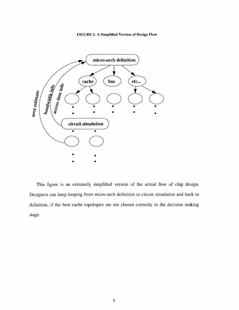
FIGURE 1. A Simplified Version of Design Flow
cache bus etc...
* 0circuit simulation
This figure is an extremely simplified version of the actual flow of chip design.
Designers can keep looping from micro-arch definition to circuit simulation and back to
definition, if the best cache topologies are not chosen correctly in the decision making
stage.
Chapter 2
Existing Work on Cache ModelingThere are publications on modeling cache access time by people in industry and
academia. Wilton and Jouppi at DEC Western Research Lab published their first cache
models in 1994 [17], then made improvements in 1996 [16]. They modeled each compo-
nent's delay in the critical path, assumed designing with 0.8 micron CMOS process, and
estimated gate delays of the critical path using Horowitz's transistor models [17]. The
transistor-level models take various input rise times and output capacitive loads into con-
sideration, which makes the analytical models more realistic than some early work done
on cache modeling. However, Horowitz's transistor models developed in 1983 might not
be adequate to model today's short channel devices. Horowitz assumed that a transistor
stack operates in linear regime and approximated on-resistance of the stack [8]. Later
Sakurai and Newton generated the "Alpha-Power Law" to model series-connected MOS-
FET circuits [14]. Sakurai proved that the delay through a transistor stack does not grow
linearly with the number of transistors in the stack, because the transistor near the output
operates in saturation regime, instead of linear regime as assumed by Horowitz. The top-
most transistor can easily enter saturation when the channel length is short. Sakurai's
model proved that Horowitz's transistor stack model to be pessimistic [13]. More recently
McFarland further developed transistor delay models by Horowitz and Sakurai [9].
McFarland used curve fitting more extensively, which involves even more mathematical
steps. All the analytical transistor models are valuable to both research and product devel-
opment. But when they are used in generating cache models like Jouppi did, the steps
involved are somewhat tedious. Wilton and Jouppi wrote a tool "Cacti" to make their mod-
els user-friendly [16]. However, as the technology process changes, adjustments need to
be made to their analytical models, in particular, Sakurai's models might be more accurate
to characterize the behavior of deep submicron devices. Also Jouppi modeled only single-
ported caches. Multiported caches have become increasingly popular, due to their micro-
architectural advantages. Furthermore, past efforts seem to have focused on obtaining
optimal partitioning of cache arrays. This thesis shows that seeking optimal partitioning is
an unnecessary, misleading, and inefficient use of design time.
One of the goals of the thesis is to compare the access time of different circuit
topologies, not the absolutely accurate delay of each cache. Certain assumptions are made
to avoid using complicated device-level analytical models to approximate cache access
time. All the existing analytical models relied on curve fitting to some extent, which
means that they must be changed as the process technology changes just like empirical
models. Simplicity is effective, robust and user-friendly. This thesis presents a spreadsheet
of access time, bandwidth, and area ratios among different cache topologies to serve as a
quick guide when selecting a particular cache topology to meet designers' needs. The data
of the spreadsheet is collected from actual circuit implementations and simulations. All
the circuits are designed and simulated in 0.25 micron process, instead of 0.8 micron used
by Jouppi.
Chapter 3
High-Level IssuesSince later chapters are dedicated to describing implementation details, this chap-
ter presents some high-level implementation issues. In today's microprocessor chip
design, neither having aggressive micro-architecture with inadequate circuit implementa-
tion nor having poor micro-architecture with fast circuits is effective in utilizing design
time and manpower. It is much more effective to optimize design of specific components,
after choosing a globally optimized structure.
How to determine a globally optimized structure is quite challenging. Different
microprocessor companies prioritize optimization features differently when designing pri-
mary caches. For instance, one primary cache design might replicate its primary cache to
double its bandwidth like DEC Alpha 21164 [5]. This introduces on-chip cache consis-
tency problems. Every time data is stored into one cache, the other primary cache must be
updated accordingly, which costs extra power. Another cache design might divide a large
cache into smaller banks to shorten array access time, but this increases interconnect
length for data to be delivered to destinations. If many loads reference to the bank that has
the longest interconnect between data output tristate buffer and destinations, the overall
latency of loading and delivering data might increase. Also, banking a large cache to
shorten access time or banking caches to increase bandwidth often involves replicating
decoders and predecoders. This kind of organization can take more area than other kinds
of cache organizations.
It consumes manpower and CPU time to design and simulate all the possible cache
topologies to analyze design trade-offs in varying cache sizes and bandwidths. The circuit
designs presented here try to globally optimize caches in speed, area, power and band-
width together as much as possible, using circuit components in the public domain. The
spreadsheet in this thesis contains a limited number of combinations but enough data to
compare the performance ratio of different globally optimized caches. The spreadsheet
contains data for 8K, 16K, & 32KByte caches which are often seen in many contemporary
designs. The next few sections present some of the high-level issues of this thesis work
which need to be noticed before diving into the details of implementation work.
3.1 Partitioning Cache Wordline and Bitline Length
Large cache line size requires buffering, which contributes to additional wordline
delay. Smaller cache line size (width of the cache) increase bitline loads (height of the
cache) which might also increase access time. This is the trade-off between cache access
time and bandwidth. As often seen in cache publications, people try or suggest finding
optimal ways to partition a cache so that the proportion of wordline length to bitline length
gives the best access time [17]. This approach is misleading and is not an efficient use of
simulation time. The bitline delay portion is really characterized by an analog circuit
because it is small signal differential amplification time, and the rest of the cache is digital.
Since analog portion of the cache cannot be pipelined, determining the geometry of a
cache should start by looking at the timing requirement first, making sure that the worst
case bitline delay does not exceed timing requirements. After determining cache height,
the wordline length is determined from the height and the size of the cache. In this work,
128 cells are attached to each pair of bit and bitbar lines, in order to generate enough small
differential signals for sense amps to detect fast. This number stays the same for all the
caches in this work, since the optimized 8kByte cache serves as the building block for
caches of larger sizes or higher bandwidths.
3.2 Determining Degree of Associativity
It is important to separate micro-architecture and circuit design trade-offs, when com-
paring access time of different circuit topologies that have same cache sizes. In this thesis,
the associativity of all the caches needs to be fixed to make objective comparisons. Way-
prediction is assumed for all cache circuits. SGI's high-end products MIPS R10000 and
R12000 both have way-prediction mechanisms [10]. Way-prediction prevents address
translation and tag array access from adding delays to data array access. In order to
achieve high hit ratio and to take advantage of way-prediction schemes, the associativity is
fixed at 4 here. This is also a circuit hack to reduce access time. Each sense amplifier can
only have a limited number of bitline pairs attached together as input to the sense amp, and
each bitline pair has to go through a column multiplexor to output line size to match bus
width. Therefore, I interleave 4 ways and use way-predication vector as column mux
select signals to
* select column with the correct way data
* eliminate a mux delay vertically down the cache
* equalize way select delay of the same bit
So now, the cache has the hit ratio of a 4-way set associative cache and delay time of a
direct-mapped cache that has the shortest access time. The circuits in this work are imple-
mented as direct-mapped caches, but they behave like associative caches as well.
3.3 Major Assumptions Made
3.3.1 Data Array Access is Critical
One major assumption made is that the critical path of all the caches is the data array
access. In modern cache designs, critical paths often include TLB (Translation Look-aside
Buffer) and tag array access to give way-select and hit / miss information. In some cases,
the clock tree datapaths for enabling sense amps is also included in the critical path.
Although the TLB outputs physical address for tag comparison, it is small and often
implemented using CAM (Content Addressable Memory) arrays or highly associative
arrays for quick virtual address translation. Tag array access is similar to data array access
with an extra delay due to comparison. But a tag array is also relatively small compared to
a data array. Therefore, the assumption is that designers should be able to design TLB and
tag array datapaths to match part of the delay of data array access and provide way select
signals early enough. For large data arrays, the arrival of hit / miss information generated
by TLBs and tag arrays becomes less critical. The data array is pipelined and needs muti-
cycles to output data. The hit/miss information needs to be available only by the end of the
last pipestage before data is used by other parts of the chip. Any other timing select signals
should also arrive early enough. Basically, designers should not let any select signals
worsen the data array latency, which sets tight timing constraints for successive pipe-
stages, this in turn, affects a processor's overall performance.
3.3.2 Begin and End of Access TimeAll the access times in this thesis refer to worst case cache read times, because
loading data is more critical than storing data. Loads can really stall pipeline. Another
assumption is that data array access time starts from address bits latching for indexing data
array to output data latching. Both physically indexed, physically tagged caches and virtu-
ally indexed, physically tagged caches have micro-architecture and circuit advantages and
disadvantages. To keep micro-architecture trade-offs separate from circuit trade-offs, the
data array latency starts after address bits become available, regardless of virtual or physi-
cal address bits, which is another reason why TLB translation is not included in the critical
path. If readers prefer to use physically indexed caches, the TLB access time is added to
data array access. But if accessing TLB is the first step for all the cache circuits, including
TLB access time does not affect cache performance comparisons significantly. Therefore,
the spreadsheet of this thesis contains all the information about data array. Readers can
extract information from the spreadsheet to estimate access times of tag arrays and TLBs,
because they are all similar arrays from the circuit implementation point of view. The
assumptions made above are a means to efficiently study area, speed, and power design
trade-offs of current high-performance caches.
3.3.3 Virtually Indexed, Physically Tagged Arrays
I made some assumptions about logic control signals for the fastest array access
time. The assumptions set micro-architectural constraints which architects need to con-
sider during architecture definition and chip floor planning. This is the bottom up commu-
nication referred to in the previous section.
The building block is assumed to be a virtually indexed, physically tagged cache.
As soon as a virtual address is available, the untranslated page offset is used to index the
data portion, bypassing address translation by the TLB. For aggressive clock frequencies,
cache access often takes more than one cycle. The actual array access pipestage in this
work starts from the domino decoder to the output load. Predecoding the array index
(wordlines) contributes to part of the delay in the previous pipestage.The time that the vir-
tual address bit travels through all the interconnect to reach the predecoder and the prede-
coding time must be less or equal to the clock period minus the required setup time of the
clock, because predecoded lines must be ready before the setup time of the domino evalu-
ation clock to avoid inadvertently flipping logic. Some readers might argue that virtually
indexed, physically tagged caches have synonym problems, meaning the same virtual
address is mapped to two different physical locations. There are methods to reduce syn-
onym problems, for example, making sure the tag array does not exceed the size of a phys-
ical page.
3.3.4 Way Prediction
Way prediction is the key to make associative caches have the access time of direct-
mapped caches as indicated in section 3.2. This scheme prevents any delay of deciding
way hit from joining the critical path, and it also eliminates the way select multiplexor in
the critical path. Therefore, way prediction schemes save both array access time and area.
Some readers might wonder how the way select information can be ready so fast. To my
best knowledge, there are several ways of implementing way prediction schemes, and
architects can certainly improve them. Both MIPS RO1k and R12k implement way predic-
tion [6]. Difference-bit caches [7] and the path balancing table [12] are also usable, but
they limit the degree of associativity.
3.3.5 Control Signals
All the control / enable signals, including way prediction information, must be
ready when they are needed. Basically, no extra delay should be introduced by enable sig-
nals to the intrinsic array delay. For instance, the sense amplifier enable signal should be
ready on time. The data path of the sense amp enable signal should be designed to be
effective early enough to sense voltage differentials. Again these constraints affect logic
and datapath designs of previous pipeline stages. They require optimal cache component
arrangement, which in turn affect floor planning of neighboring FUBs (Function Unit
Blocks). The constraints are nontrivial to satisfy. This surely involves design trade-offs in
designing neighboring FUBs. But it is important to keep in mind that building the fastest
primary caches is the top priority, because they directly affect data utilization rate, which
in turn affect the flow through of pipeline stages. Readers can argue that out-of-order
instruction execution can hide cache access latency. However, out-of-order or speculative
execution is effective only when there is no data-dependency or structural hazard. It is still
essential to have fast cache array access and then use out-of-order execution to hide the
latency that takes to deliver data via bus interconnect, which has become increasingly
harder to manage as the process technology continues to scale down.
3.3.6 Neighboring FUBs
Neighboring FUBs need to be arranged to allow data to be quickly delivered to
destinations. This requirement makes floorplanning challenging, because this might
increase interconnect length for later pipestages. It is even more difficult to optimize inter-
connect delays for those microprocessors that use unified caches. A unified cache stores
both instructions and data. Since cached data and instructions are dispatched to different
locations, the shortest route to pass data might not be the optimal path for instruction pass-
ing. Applying Rent's rule to predict on-chip interconnect density during architectural plan-
ning is helpful.
Chapter 4
Implementation Details and Circuits
4.1 Introduce an Optimized Building Block
The simplest formulae, having fewest variables, are often the most powerful ones
that can capture a wide range of patterns in phenomena and behaviors of matter. For exam-
ple, Newton's F=ma is the simplest formula, yet the most powerful law that creates and
governs numerous technological disciplines, and affects many aspects of our lives.
Inspired by the simplicity and power of Newton's law, I decide to create a simple building
block, then build abstractions based on the fundamental unit to cover more cache imple-
mentation possibilities. However, the building block itself must be relatively optimized to
be meaningful in researching high-performance caches. Readers might think that having a
highly optimized building block conflicts with achieving simplicity. Fortunately, the fast-
est cache, a direct-mapped cache, is the one that has the simplest or minimum number of
logic stages in the critical path. Prior to implementing fast circuits, the crucial step is min-
imizing the number of logic stages in the critical path of accessing caches.
The critical path of accessing a direct-mapped cache begins at the address bits
latch, traverses through a predecoder, then the interconnect that has the height of the array,
a decoder, turns all the way to the last bit cell hanging off the top word line, goes all the
way down to the last bit cell hanging off of the bitlines, then goes through a column selec-
tor, a sense amplifier, then drives the output load. For associative caches, there is an addi-
tional delay introduced by the multiplexor that selects between ways. In many modern
microprocessors, primary caches are at least 2-way set associative. Associativity reduces
address conflict, but the hit ratio of a cache does not increase infinitely with the degree of
associativity. Also, without optimization, usually the higher the degree of associativity, the
slower the caches are. This is because the number of input to the way-select multiplexor is
larger, meaning more pass gates (transmission gates) are tied together which contributes
more diffusion capacitance to slow down the circuit. It does not make any sense to say that
a direct-mapped cache performs better than a two-way set associative cache, because the
former has shorter access time. This is like comparing apples with oranges. Set associative
caches have microarchitechtural advantages, while direct-mapped caches have circuit
advantages. Some microprocessors have 2-way set associative caches, while others have
more than 2-way. It is also nonsense to compare the performance among these caches,
because their hit ratios differ. The 2-way associative caches are faster, but the hit ratio is
lower. which triggers more accesses to on-chip or off-chip secondary caches, degrading
the processor's overall performance.
The building block (see Figure 4.1), which is used to analyze caches, optimizes
cache performance both in micro-architecture and circuit topology. The key to building a
high-performance cache is to achieve the hit ratio of associative caches and the access
time of direct-mapped caches. It is crucial to maintain direct-mapped cache access,
because those caches use a minimum number of logic stages needed for a functional
cache.
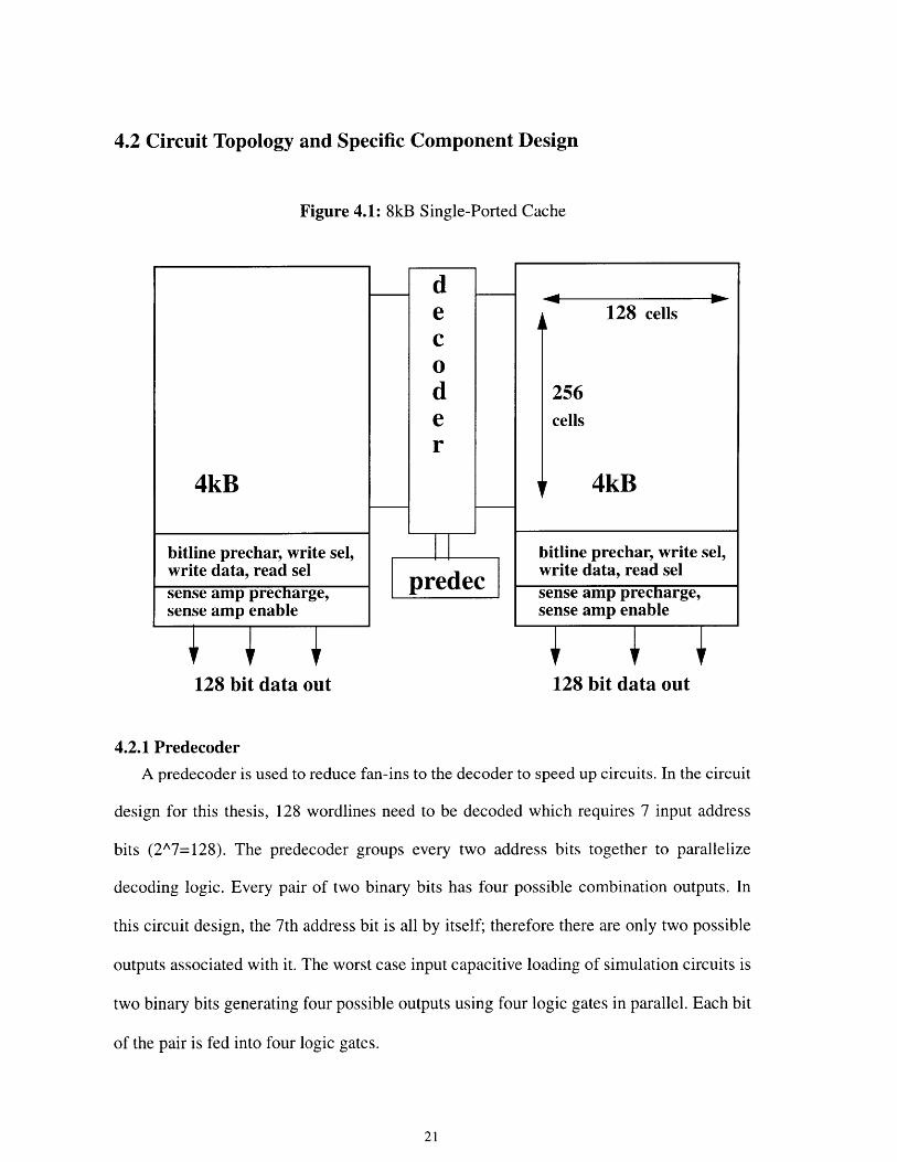
4.2 Circuit Topology and Specific Component Design
Figure 4.1: 8kB Single-Ported Cache
4kB
bitline prechar, write sel,write data, read selsense amp precharge,sense amp enable
128 bit data out
dec
der
predec
128 cells
256cells
4kB
bitline prechar, write sel,write data, read selsense amp precharge,sense amp enable
128 bit data out
4.2.1 Predecoder
A predecoder is used to reduce fan-ins to the decoder to speed up circuits. In the circuit
design for this thesis, 128 wordlines need to be decoded which requires 7 input address
bits (2^7=128). The predecoder groups every two address bits together to parallelize
decoding logic. Every pair of two binary bits has four possible combination outputs. In
this circuit design, the 7th address bit is all by itself; therefore there are only two possible
outputs associated with it. The worst case input capacitive loading of simulation circuits is
two binary bits generating four possible outputs using four logic gates in parallel. Each bit
of the pair is fed into four logic gates.
4.2.2 Decoder
After the predecoding stage, the predecoded wordlines see interconnect that has a
length of the array's height in the worst case delay. This interconnect is modeled during
simulation as part of output load of the predecoder and input load to the decoder. Since
two address bits predecode into four lines, each of the four is then fed into thirty-two par-
allel logic gates in the decoder, which generates 128 different wordlines. Each of the logic
gates is a 4-input nand or nor gate, depending on how many inversion logic gates address
bits go through to reach the decoder. In array designs, the use of dynamic gates should be
minimized to reduce dynamic power consumption. In this design, only the decoding stage
uses domino gates. Extra care is needed when using domino gates to prevent various noise
and charge sharing problems.
4.2.3 Wordline Loads
Wordlines that come out of decoders need to travel across the array to reach the last bit
cell in each row; therefore, when building simulation circuits, all the capacitive loads seen
by the wordlines in actual arrays must be included. Interconnect delay has become
increasingly difficult to deal with as the process technology continues to scale down. How-
ever, wordlines of arrays are quite manageable compared to bus interconnect for three rea-
sons. The first reason is that all the bit cells are closely abutted, the capacitance of
wordlines is dominated by gate capacitance of passgates in each bit cell, instead of wire
capacitance. The other reason is that wordlines are widely apart from each other due to bit
cell height, meaning not much coupling between wordlines of adjacent rows. The last rea-
son is that wordlines from adjacent rows generally do not switch to opposite polarity at the
same time, since only one wordline can be on at a time and the wordline is turned off
before its neighboring wordline is fully decoded. When adjacent wires change to opposite
polarity at the same time, the cross coupling of wires is doubled as is often seen in bus
interconnect. Therefore wordlines of arrays capacitance and resistance are scalable as pro-
cess changes.
4.2.4 Bit Cells
Each bit cell, which is the most commonly used RAM cell, has six transistors. The
transistors should be minimally sized in order to minimize the total cache area. The gates
of the two passgates inside each cell are tied to a wordline, and the drain / source of the
two passgates are connected to a pair of bit and bitbar lines respectively. The other four
transistors are two back to back inverters to latch data. Certain sizing ratios among the six
transistors must be maintained to avoid inadvertent flipping of logic.
4.2.5 Bitline Loads
Bitlines loads directly impact on the rate of detection of differential signals. Bitline
capacitive loads are mostly drain capacitance of passgates in all the cells that share the
same bitlines. Other capacitance comes from drain capacitance of write buffers, read-
select muxes, data-in and precharge devices. The bitline of one cell and bit barline from its
neighboring cell can cross couple, introducing additional delay which might be severe
enough to flip logic. Therefore, bitlines must be carefully laid out to decouple from each
other to minimize neighboring interference.
4.2.6 Precharge, Write Buffer, and Read Mux
When the array is not being read, bit and bitbar lines must all be precharged to high to
prepare for stores. Typically there is an equalizer, which is one passgate, to maintain equal
voltage of the lines. Precharge circuitry must be placed above read select mux on bitlines.
The write buffer, as the names suggests, is for storing information into bit cells. Each bit-
line (bit and bitbar) has an nfet attached to it. Write-enables control the gate of nfets, and
data is connected to the other end of nfets. When the write enable is on, data is written
onto the bitlines through the turned-on nfet. The read mux is basically designed with tran-
sistors connected in series with bitlines. Read-enables turn on the nfets, then information
on the bitlines pass through the nfets flow into sense amplifiers.
4.2.7 Sense Amplifier Precharge and Sense Amplifier
The sense amplifier precharge circuitry is the same as regular precharge, and it is nec-
essary to place it below the read mux and above the sense amplifier. It is the same as regu-
lar precharge circuitry, except it needs to be specifically placed on bitlines below the read
mux and before the sense amplifier to make sure that both bitline ends of the read mux
truly start with equipotential before sensing. The sense amplifier is really an analog differ-
ential amplifier that amplifies different voltages on bitlines and corresponding bitbar lines.
It should be turned on after a certain differential voltage level is reached, otherwise, it
could sense the wrong data due to noise interference. The sense amplifier is triggered by a
timer which can turn it on at a precise time to quickly detect and amplify signals without
making mistakes. Designers need to look at circuit simulation of bitlines and record the
time that at where the correct differential voltage occurs.
4.2.8 Output Loads Modeling
Since this thesis is intended to make a systematically quantitative analysis of cache
behavior, I try to cover as many cache topologies as possible to make data analysis realis-
tic. Modeling output loads of sense amps is crucial, because it propagates gain information
backwards which affects transistor sizing of previous logic stages. By examining various
cache topologies, I conclude that the output loads of senseamps of an array can have six
possibilities. The data that comes out of a sense amp is fed into 1) a latch; 2)a mux; 3)sev-
eral hundred micron long interconnect; 4) a tristate driver; 5)a logic gate; or 6) an inverter
to drive interconnect. I measure the capacitance of each possibility seen by data out and
use it as the worst case capacitive loads to size circuits backward.
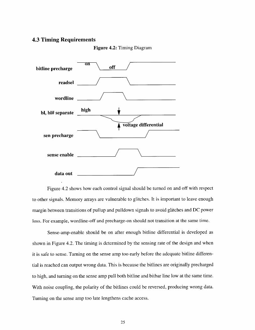
4.3 Timing Requirements
Figure 4.2: Timing Diagram
bitline precharge
readsel
wordline
bl, bl# separate
sen precharge
sense enable
high
voltage differential
data out
Figure 4.2 shows how each control signal should be turned on and off with respect
to other signals. Memory arrays are vulnerable to glitches. It is important to leave enough
margin between transitions of pullup and pulldown signals to avoid glitches and DC power
loss. For example, wordline-off and precharge-on should not transition at the same time.
Sense-amp-enable should be on after enough bitline differential is developed as
shown in Figure 4.2. The timing is determined by the sensing rate of the design and when
it is safe to sense. Turning on the sense amp too early before the adequate bitline differen-
tial is reached can output wrong data. This is because the bitlines are originally precharged
to high, and turning on the sense amp pull both bitline and bitbar line low at the same time.
With noise coupling, the polarity of the bitlines could be reversed, producing wrong data.
Turning on the sense amp too late lengthens cache access.
on \\ off /
q
The most important timing requirement is to overlap bitline precharge with sens-
ing. This is critical for satisfying multi-cache access in one clock cycle. After many trials,
I discover that it is safe to close the bitline soon after the adequate bitline differential is
developed. This allows precharging to start before data is out. DEC Alpha 21264 has sin-
gle-ported primary caches and double pump data in one clock cycle, essentially each read
can use only half of a clock cycle to finish [5]. This might not be achieved if the clock
speed is even more aggressive than Alpha's and if clock skew and jitter are severe. By
overlapping bitline precharge with data sensing in a truly physically dual-ported cache, a
read can take the clock cycle using one port, a write can also be satisfied in the same cycle
using the second port. Or, issuing two load requests during the same or adjacent clock
phase can be satisfied.
4.4 Building Abstractions
4.4.1 16kB Single-Ported Caches
Having the building block done, it is time to build abstractions on top of it. It is
interesting to see how a cache's behavior changes when its size is increased. As stated
before, having a larger cache can reduce address conflict, thereby increasing hit ratio. To
look at it from another angle, increasing the size can also increase the bandwidth of the
cache, depending on the width of the data bus.
One way of implementing the 16 kB cache using the building block is to replicate
the 8kB cache array and all the peripheral circuits, and place them symmetrically so that
the address bits can reach both predecoders at the same time. Replicating caches allows
the access time to stay the same as that of the 8kB and doubles the original bandwidth.
The trade-off is that replication introduces on-chip cache consistency management. Every
time one cache is updated, the twin copy also needs to be updated, wasting power. The
activity factor of arrays should be kept low to save power. Another trade-off is replicating
decoder and predecoder costs extra area.
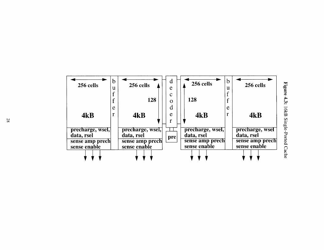
The other way of implementing the 16kB using the building block is to internally
buffer wordlines (see Figure 4.3). The buffer for each wordline introduces some additional
area, but it is relatively smaller compared to having an extra set of a decoder and a prede-
coder. Buffers add a little more delay, but they can also speedup wordline for the second
8kB array. This is because the decoder fans out symmetrically in two directions, seeing
twice the wordline loads and interconnect. The buffer in a wordline sees only one set of
wordline loads and interconnect. Having two 8kB array adjacent to each other might make
the final data out travel some extra interconnect in successive pipestages, depending on
how data is dispatched with respect to the location of the arrays. With optimal sizing, the
16kB with internal buffering can still have array access done in one clock cycle.
256 cells
4kB
precharge, wsel,data, rselsense amp prechsense enable
256 cells
128
4kB
precharge, wsel,data, rselsense amp prechsense enable
4**
C0oder
256 cells
128
4kB
precharge, wsel,data, rselsense amp prechsense enable
256 cells
4kB
precharge, wseldata, rselsense amp prechsense enable
4.4.2 32kB Single-Ported Caches
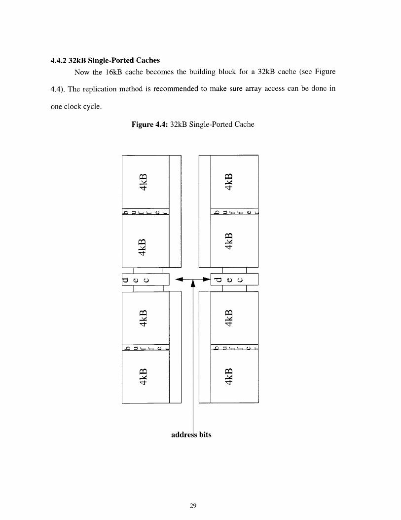
Now the 16kB cache becomes the building block for a 32kB cache (see Figure
4.4). The replication method is recommended to make sure array access can be done in
one clock cycle.
Figure 4.4: 32kB Single-Ported Cache
1) 3 ce Ic 6I-
addreds bits
a) O1
rd a, oL
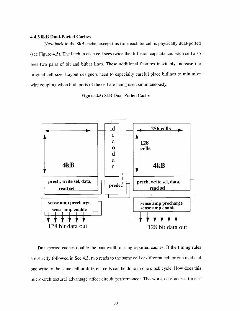
4.4.3 8kB Dual-Ported Caches
Now back to the 8kB cache, except this time each bit cell is physically dual-ported
(see Figure 4.5). The latch in each cell sees twice the diffusion capacitance. Each cell also
sees two pairs of bit and bitbar lines. These additional features inevitably increase the
original cell size. Layout designers need to especially careful place bitlines to minimize
wire coupling when both ports of the cell are being used simultaneously.
Figure 4.5: 8kB Dual-Ported Cache
128 bit data out 128 bit data out
Dual-ported caches double the bandwidth of single-ported caches. If the timing rules
are strictly followed in Sec 4.3, two reads to the same cell or different cell or one read and
one write to the same cell or different cells can be done in one clock cycle. How does this
micro-architectural advantage affect circuit performance? The worst case access time is
when having two reads to the same cell because all the capacitive loads of the single-
ported cell are doubled. However, this does not mean the array access is twice as slow,
since reading bitlines is a small signal operation, only detecting bitline differential mat-
ters, instead of developing full rail to rail signals. The area increase does make wordlines
and bitlines somewhat longer. Good layout designs do not make the interconnect twice as
long as that of a single-ported cache. The interconnect within memory array is much more
manageable than bus interconnect because bit cells are so closely abutted and gate and
drain capacitance dominates over wire capacitance. Wordlines and bitlines are separated
by transistors, so cross coupling is not severe. Another difference between memory and
bus interconnect is that memory wires never have a Miller factor of 2. Current in word-
lines all move in the same direction, from the decoder to the cell. For dual-ported array, if
two adjacent cells are doing read and write respectively at the same time, each bitline sees
only one opposite transition occurring in the wire of its neighboring cells.
A dual-ported cache can also finish an array access in one clock cycle. An impor-
tant control signal requirement is that there should be two sets of enable signals for the
two ports within each cell to satisfy one load and one store in the same cell using one
clock cycle. Therefore, compared to single-ported caches, dual-ported caches take twice
the area, double bandwidth, and can also have array access done in one clock cycle with
careful sizing devices. The 8kB dual-ported cache is now the building block for a larger
dual-ported array, just like the 8kB single-ported cache
4.5 Process IndependentThe circuits are designed so that the performance ratios obtained are process inde-
pendent, because all the different cache topologies use the same 8kbyte cache building
block. This means that transistor sizing of all the peripheral circuits stay the same. Single-
ported and dual-ported have different bitcell sizes which contribute to differences in
arrays' heights and widths. Decoders of dual-ported caches see a longer interconnect, but
the decoders of the single-ported caches are sized to be able to tolerate a few hundred
micron interconnect differences. Also, the interconnect within cache array is much more
manageable than bus interconnect, because wordline capacitance is dominated by gate
capacitance and bitline capacitance is dominated by diffusion capacitance because array
cells are closely abutted together. Transistor capacitances are linearly scalable with pro-
cess change. Therefore the array access time ratio among caches stay roughly the same for
new process technologies which allow the information provided by this thesis to serve as a
reference for future cache studies and designs.
Chapter 5
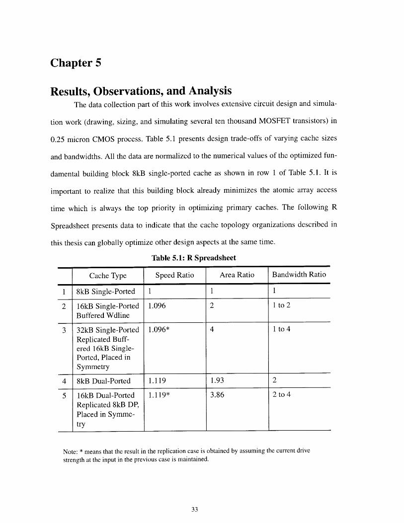
Results, Observations, and AnalysisThe data collection part of this work involves extensive circuit design and simula-
tion work (drawing, sizing, and simulating several ten thousand MOSFET transistors) in
0.25 micron CMOS process. Table 5.1 presents design trade-offs of varying cache sizes
and bandwidths. All the data are normalized to the numerical values of the optimized fun-
damental building block 8kB single-ported cache as shown in row 1 of Table 5.1. It is
important to realize that this building block already minimizes the atomic array access
time which is always the top priority in optimizing primary caches. The following R
Spreadsheet presents data to indicate that the cache topology organizations described in
this thesis can globally optimize other design aspects at the same time.
Table 5.1: R Spreadsheet
Cache Type Speed Ratio Area Ratio Bandwidth Ratio
1 8kB Single-Ported 1 1 1
2 16kB Single-Ported 1.096 2 1 to 2Buffered Wdline
3 32kB Single-Ported 1.096* 4 1 to 4Replicated Buff-ered 16kB Single-Ported, Placed inSymmetry
4 8kB Dual-Ported 1.119 1.93 2
5 16kB Dual-Ported 1.119* 3.86 2 to 4Replicated 8kB DP,Placed in Symme-try
Note: * means that the result in the replication case is obtained by assuming the current drivestrength at the input in the previous case is maintained.
5.1 Doubling Cache Size and Minimizing Area
Doubling the 8kB cache size does not double the access time. In fact, the access time
increases by only 9.6%, if the cache is implemented using the cache type in row 2 of Table
5.1. When a 16kB cache is implemented as Figure 4.3, the extra delay is primarily intro-
duced by the wordline delay through the first 8kbyte and the delay of the wordline buffer
between it and the second array. All the other circuit delays stay the same. This 16kbyte
cache is pseudo cache banking. The cache is really split in half and has the option to be
used as a bigger cache to store information or to be used to double output data. This is why
the 16kB single-ported cache can either remain the same or double the bandwidth of the
8kB single-ported cache, depending on a designer's choice. The area of this 16kB is
roughly doubled because the buffers need to be large enough to optimize the delay of
wordlines and other control signals that travel in the same direction as the wordlines.
For smaller size caches like 16kB, I suggest using wordline buffering (buffering word-
lines between two optimized 8kB) as described above, instead of replicating caches as
seen in some microprocessor designs. Replication can achieve the same access time as the
8kB. However, power consumption doubles every time one of the two 8kB is updated, in
order to maintain cache consistency. Also, only placing the replicated cache symmetrically
as the mirror image of the original 8kB allows the access time to remain the same as that
of the 8kB. If the floor plan of neighboring FUBs only allow the two 8kB caches to be
placed adjacently, then this replication scheme increases access time in the worst case
delay. This scheme increases area more than the wordline buffering technique due to extra
routing signals to reach the second 8kB, in addition to increasing power consumption.
Buffering wordlines and Replicating caches as mentioned above are basically 2 types
of the cache banking technique. When banking large caches, the height of the cache (the
analog portion) is determined by whether reading bitlines can be done within one clock
cycle, because this analog portion of the array cannot be pipelined as mentioned in Section
3.1. Once the height is determined, then designers need to balance the width of each bank
with the total number of banks.
Number of Banks = Cache Size / Bank Size (5.1)
Bank Size= Width * Height (5.2)
Time to Read the Height of each array < 1 Clock Period of the Current Domain (5.3)
When designing large caches, the time to propagate data through the interconnect
between cache data-out and various destinations affects the arrangement of banks, which
in turn limits the total number of banks. Because of neighboring FUBs' locations, cache
banks cannot be arbitrarily placed; otherwise it causes data to travel longer routes to reach
destinations in successive pipeline stages. Having fast cache array access but traveling
much longer interconnect to reach destinations, resulting in more pipestages, can unfavor-
ably increase overall load latencies. Designers need to consider how much time margin
there is in the pipestage after accessing caches, and use Equations 5.1, 5.2, 5.3 together to
arrange cache topologies. Section 5.2 gives an example of minimizing the interconnect
delay after cache access.
5.2 Quadrupling the Cache Size or Bandwidth
Having a 32kB cache can certainly increase cache hit ratio, but by how much would
quadrupling the cache size of 8kB increase the access time? If the 32kB is arranged as
suggested here, the access time only increases by 9.6% from the access time of the 8kB as
shown in row 3 of Table 5.1. Designers should replicate the 16kB single-ported cache and
place the two identical 16kB symmetrically. And each of the 16kB should be built from
the 8kB by buffering wordlines. Again the bandwidth ratio could be two to four, depend-
ing on designers' needs. The area of this 32kB is roughly quadrupled, less than the area
needed for other kinds of topologies, because this cache organization tries to minimize the
area consumed by interconnect. On modern microprocessor chips, the area is determined
by interconnect density rather than transistor density.
5.3 Doubling Bandwidth
5.3.1 Minimizing Area and Increasing Some Access Time
In order to double cache bandwidth and minimize area, I suggest to use a dual-ported
cache as shown in row 4 of Table 5.1. The dual-ported cache has additional delay on the
bitlines because each bit cell sees at least twice the capacitive loads down the bitlines. The
access time is increased by 11.9%, compared to that of the 8kB single-ported. However,
the area is only 1.93 times that of the 8kB instead of twice, which is a substantial saving
for much larger caches. Dual-ported cache has a micro-architectural advantage. With the
timing requirement described in Section 4.4, the dual-ported cache allows back to back
loads and stores in one clock cycle, thereby doubling cache bandwidth.
5.3.1 Minimizing Access Time, Increasing Area and Power
If a designer's goal is to minimize access time and double bandwidth, the replication
method works well. The implementation is to replicate the entire 8kB single-ported cache
and place the two caches symmetrically to minimize interconnect length, so that the two
caches can output data in the same time as a single 8kbyte cache. This is true only if the
current drive strength at the input of the single 8kbyte cache is maintained at the input of
this replication topology. This makes the circuits before the cache slightly slower because
of the relatively small capacitance of the additional latch. As mentioned in Section 5.1, the
trade-off is that extra power is consumed in order to maintain cache consistency between
the two. The two caches are decoded using the exact same address bits, and the two store
the same data. Every time data is stored in one cache, the other cache must be updated too.
Writing into cache involves powering up the entire 8kB array. Also placing two caches
symmetrically affects the floor-planning of neighboring Function Unit Blocks, putting
pressure on other FUB designs because they might see longer interconnect delays.
5.4 Doubling Cache Size, Quadrupling Bandwidth without Quadrupling Area
The best way to quadruple the bandwidth of the 8kB without quadrupling the area is to
use a 16kB dual-ported cache by replicating 8kB dual-ported and place the two banks
symmetrically. The area ratio is 3.86 (see row 5 of Table 5.1) instead of 4 by replicating
the 8kB or internally banking into multiples of 8kB.
5.5 Power Issues
Lowering microprocessor power dissipation is one of the most important design issues
nowadays in order to meet customers' needs, especially for mobile computing and hand-
held products. Every chip maker continues to increase the clock speed to achieve faster
computing.
Dynamic Power Dissipated = C*VA2*F*A (5.4)
C=Capacitance (proportional to area), V=Power Supply Voltage,
F=Clock Frequency, A=Activity Factor
Equation 5.4 indicates four factors that affect dynamic power dissipation. As men-
tioned in Section 4.2.2, minimizing the use of dynamic circuits reduces dynamic power
dissipation due to high switching frequencies. Since F continues to increase, lowering V is
a popular method because the power decreases quadratically. However, V cannot be
brought lower than semiconductor device operating voltages, which leaves the options of
lowering C and A. Reducing area consumption certainly lowers C. Since the total on-chip
array area is at least 40% of the total die area, reducing array area has a noticeable effect
on lowering C. The area of each bit cell should be minimized, meaning the minimally
allowable sizes should be assigned to the six transistors of each cell as mentioned in Sec-
tion 4.2.4. For 16kB primary caches, buffering wordlines between two 8kB banks is more
desirable than replicating one 8kB cache bank as mentioned in Section 5.1. The extra set
of one decoder and one predecoder costs more area than the total area of buffers. Buffering
wordlines costs more access time than replication, but for caches of this size, buffering
does not significantly increase cache access time. Finally, lowering the activity factor of
cache arrays, that is, powering arrays down when they are not needed, also decreases
power consumption. This topic is a specific implementation detail; therefore, it is not dis-
cussed further.
5.6 A Few Cautionary Words
Before designing the circuits, I make certain assumptions already listed in Chapter 3.
The assumptions are realistic and practical for readers to consider when they try to select
the best cache topologies to meet their own specifications. I use circuit components in the
public domain to design the caches listed in the spreadsheet to allow a wide range of users
to consider and apply my design strategies. Chapter 4 describes implementation details of
the reference frame. The numerical values that I use for the array dimensions are not
magic numbers. Readers should pay more attention to the approaches. All the approaches
listed are valid for implementing both direct-mapped and associative caches. The actual
circuit designs here are really the circuit implementations of direct-mapped caches; how-
ever, I assume way-predication mechanisms are available to make the circuits behave like
associative caches (see Section 3.2 and 3.3.4). This thesis is not intended to tell readers
that the design strategies listed here are the ultimate optimization techniques for final pro-
duction circuit designs. However, this thesis provides globally optimized structures as
starting points to help users efficiently choose the right cache topologies to meet their
needs. Users can then use various circuit hacks to do local optimizations to obtain even
better speed ratio [2], [4], and [ 11]. These local optimizations are implementation details
set by individual organizations. The data in the spreadsheet is process-independent so it
can serve as a reference for future process technology designs as well.
Chapter 6
Conclusion
6.1 Summary of the ResearchThe primary goal of this thesis was to systematically and quantitatively analyze perfor-
mance trade-offs of major cache topologies. It is difficult to compare the performance of
different cache implementations, because they have different specifications and are
designed with different circuit and simulation methodologies. In order to make objective
comparisons, I first established a reference frame by using circuit components in the pub-
lic domain to design the frame. While designing the reference frame, I realized that I
would need to design a building block and to use it consistently in implementing caches
with different sizes and bandwidths. More importantly, the building block had to be opti-
mized in speed, so that the reference frame would be a truly effective, meaningful tool for
comparing cache performance. In the meantime, I strove to design circuitry so the results
would be process-independent. I optimized the building block to obtain the hit ratio of an
associative cache and the access time of a direct-mapped cache. After finishing the build-
ing block, I designed and simulated caches with different sizes and bandwidths, then col-
lected data for the spreadsheet.
Although the R Spreadsheet looks simple, it has high information content. It shows
how to optimize area and / or bandwidth in addition to optimizing speed. The most chal-
lenging part of the work was to efficiently and effectively organize circuit topologies:
Without depending on specific implementation details of any existing cache work, the
designs in this thesis include a variety of high-performance cache implementations along
with my own design strategies. Fortunately efficient ways were found to optimize caches
in speed, bandwidth, and area, all three, providing different cache topology choices with
similar performances. As a result of these efficient approaches, the spreadsheet represents
a variety of cache implementation schemes.
Based on the data collected from realistic cache designs and simulations of several
ten thousand transistors, the thesis describes design trade-offs and design considerations
for concurrent high-performance caches which can serve as a convenient reference for
designers during the topology definition phase. This quick reference shows how the
behavior of caches change as their sizes and bandwidths are increased. The performance
ratios presented are accurate for new process technologies because they are process-inde-
pendent. Section 5.5 points out how readers should interpret the spreadsheet.
6.2 Expansions Based on the GroundworkThis thesis focuses on optimizing data arrays of primary caches (see Section
3.3.1). The approaches can be applied to analyzing tag arrays. The main additional fea-
tures of tag arrays are comparators, and the rest of the components of tag arrays are the
same as those of data arrays. The work presented here can be extended to analyze and
design any on-chip or off-chip cache. For example, 3-D visualization is currently one of
the main forces pushing the computing industry. Graphic chips must have high-bandwidth
and fast caches. The results of this thesis can certainly be applied to designing high-speed
and high-bandwidth SRAMS for computer graphic applications.
6.3 Future Outlook of Memory DesignsOut-of-order instruction execution [3] and non-blocking caching techniques will
continue to be employed to help hide cache latency. Further explorations of way-predic-
tion schemes are needed, because they are a powerful means of reducing access time [1].
Way-predictions require fast tag array access and effective recording of tag array access
patterns. More levels of on-chip cache hierarchy can be introduced to reduce overall data

access time and cache miss penalty. However, adding more levels of cache along with
increasing bandwidth will inevitably increase total cache area, thereby die area, which in
turn, will increase fabrication cost within the same process technology. Bringing DRAM
on-chip has been a continuing effort made by industry and academia [15]. The most attrac-
tive thing about a DRAM is its high density. However, the drastically different DRAM
process technology hinders the integration of a DRAM and the rest of the chip. Also,
DRAMs have thermal tolerance different from other components of the chip. The increas-
ing demand for high cache bandwidth will trigger innovative process integration technolo-
gies to be developed probably at higher costs initially. If DRAMS are indeed brought onto
widely sold commercial chips one day, it will bring revolutionary changes to computer
architecture and chip design.
References
[1] J. Bennett and M. Flynn, "Reducing Cache Miss Rates using Prediction Caches."Stanford Technical Report No. CSL-TR-96-707, Oct 1996.
[2] T. Chappell, B. Chappell, S. Schuster, J. Allan, S. Klepner, R. Joshi, and R. Franch,"A 2-ns Cycle, 3.8-ns Access 512-kb CMOS ECL SRAM with a Fully PipelinedArchitecture." IEEE Journal of Solid-State Circuits, vol. 26, no. 11, pp. 1577-1585,Nov. 1991.
[3] Digital Semiconductor, DEC, Stanford, "A 600 Mhz Superscalar RISC Microproces-sor with Out-of-Order Execution." International Solid-State Circuit Conference1997, pp. 393-396, 451, Feb. 1997.
[4] P. Gronowski, "Designing High Performance Microprocessors." Digital Semiconduc-tor and DEC, 1997 Symposium on VLSI Circuits Digest of Technical Papers, pp. 51-54, July 1997.
[5] Linley Gwennap, "Digital 21264 Sets New Standard." Microprocessor Report, pp. 11-16, Oct. 1996.
[6] Linley Gwennap, "MIPS Roadmap Focuses on Bandwidth." Microprocessor Report,pp.14-16, May 1997.
[7] T. Juan, T. Lang, and J. Navarro, "The Difference-bit Cache." Computer ArchitectureNews, vol. 24, no. 2, May 1996.
[8] M. Horowitz, Ph.D thesis -- "Timing Models for MOS Circuits." Stanford TechnicalReport No. SEL83-003, Dec. 1983.
[9] G. McFarland and M. Flynn, "Delay Models for CMOS Circuits." Stanford TechnicalReport CSL-TR-95-672, Dec. 1995
[10] MIPS Technologies, Inc. "R10000 Microprocessor Product Overview." MIPS OpenRISC Technology, MIPS Technologies, Incorporated, Oct. 1994.
[11] K. Nowka and M. Flynn, "Wave Pipelining of High Performance CMOS StaticRAM." Stanford Technical Report CSL-TR-94-615, Jan. 1994.
[12] J-K. Peir, W. Hsu, H. Young, and S. Ong, "Improved Cache Performance with Bal-anced Tag and Data Paths." ASPLOS-VII (Architectural Support for ProgrammingLanguages and Operating Systems Seventh International Conference) Proceedings,pp. 268-278, Oct. 1996.
[13] T. Sakurai and A. R. Newton, "Delay Analysis of Series-Connected MOSFET Cir-cuits." IEEE Journal of Solid-State Circuits, vol. 26, no. 2, pp. 122-131, Feb. 1991.
[14] T. Sakurai and R. Newton, "Alpha-Power Las MOSFET Model and its Applicationsto CMOS Inverter Delay and Other Formulas." IEEE Journal of Solid-State Circuits,vol. 25, no. 2, pp. 584-593, April 1990.
[15] K. M. Wilson and K. Olukotun, "Designing High Bandwidth On-Chip Caches."[16] S. Wilton and N.P. Jouppi, "CACTI: An Enhanced Access and Cycle Time Model,"
IEEE Journal of solid-State Circuits, vol. 31, no. 5, pp. 677-688, May 1996.[17] S. Wilton and N.P. Jouppi, "An Enhanced Access and Cycle Time Model for On-Chip
Caches." DEC WRL Publications, July 1994.