on different methods to combine cable information into near-field data for far-field estimation
TRANSCRIPT

On Different Methods to Combine Cable Information into Near-field Data for Far-field
EstimationKeong Kam #1, Andriy Radchenko #2, David Pommerenke #3
# EMC Laboratory, Missouri University of Science and Technology4000 Enterprise Dr. Rolla, MO 65401, USA
1 [email protected] [email protected]
Abstract— Near-field scanning is often used to solve EMC problems. Aside from the purpose of visualization of near-fields,measured near-field data can be used to estimate far-field. One of many challenges associated with using near-field to far-field transform (NFFFT) technique for EMC application is the handling of attached cables. The objective of this investigation isto evaluate different methods to add cable information to the near-field data for far-field estimation. The investigation is carried out using numerical experiments in EMCoS EMC studio, which is a commercial MoM (Method of Moment) tool for EM simulation. Measurement results from a test structure are also presented to validate the simulation results.
I. INTRODUCTION
Near-field scanning is often used to solve EMC problems[1-5]. Near-field scanning allows to visualize the field distribution, often directly showing sources and hinting at possible coupling paths. Aside from this purpose, measured near-field data can be used to estimate the far-field. This near-field to far-field transformation (NFFFT) technique has been around for many decades and has found many useful applications such as antenna characterization.
On the other hand, NFFFT technique can be used in EMC application [6,7] . There are many near-field measurement challenges (phase measurement, limited dynamic range and probe sensitivity, etc.) as well as difficulties in the post processing (processing with limited/partial data, source reconstruction, etc.) One of them being how to deal with cables attached to the DUT.
Most DUTs require at least a power cable, thus including a cable into the NFFFT becomes almost a necessary step in order to estimate the correct far-field in a practical settings.Many authors have treated the emissions of PCBs with attached cables [8-13] focusing mainly on the radiation due to the antenna formed by the PCB and cable. However, toanalyse a system where the direct PCB radiation and cable radiation coexist, using near-field to far-field transformation, one possible, simple approach is to scan around the entire DUT and cable. This method should predict the far-field correctly, but scanning around the entire length of the cable is not only impractical, but also defeats the purpose of using
NFFFT, which is to get a quick estimate of the far-field radiation.
Aside from this simple, but yet impractical approach, there are several possible approaches. In this paper, we will investigate different possibilities to add cable information to the near-field data for far-field estimation. The investigation is carried out using numerical experiments using a commercial MoM tool for EM simulation [14].
II. BASIC PRINCIPLE
Different approaches can be used to obtain the far field from the near field. We base our investigations on Surface Equivalence Principle, or otherwise known as Huygens’Principle.
Fig. 1 Huygens’ Principle
The left side of Fig. 1 shows the original source J1 and M1inside a surface S, and the right figure shows the equivalent model constructed from equivalent surface currents (Js and Ms)on S. Huygens’ principle states that the sources inside the surface S can be replaced by equivalent sources that produces the same field outside the surface S. [15] The equivalent sources on the surface of the equivalent model can be calculated by:
Js = n̂ × H1
Ms = −n̂ × E1
⎧⎨⎩
This means knowing the tangential components of the near-field can be used to construct the equivalent sources on the surface.
μ0, ε0J1
M1
μ0, ε0
E1, H1
E1, H1
μ0, ε0
Js = n̂ × H1
Ms = −n̂ × E1
μ0, ε0
E, H = 0
E1, H1
S
S
978-1-4673-2060-3/12/$31.00 ©2012 IEEE 294

Fig. 2. Test Structure for Numerical Experiments
For the numerical investigation, a simple PCB model was created in a commercial MoM software [14] as shown in Fig. 2. The test structure contains a thin wire structure above a 100mm X 50mm ground plane, driven with a voltage source and terminated with a 50Ω load. The Far-field from this structure placed 1m above an infinite ground plane was calculated and maximized using heights of 1, 2 and 3m. To illustrate the NFFFT based on Huygens’ principle, near-field data was extracted from the full model as shown in Fig. 3 to calculate the far-field from this near-field data. The near-field data was extracted at 1cm away from the PCB from all six sides forming a rectangular box. Fig. 4 shows the comparison of the simulated far-field from the full model versus that calculated from the near-field data.
Fig. 3. Near-field Extraction from Full Model
From Fig. 4, it can be seen that the far-field calculated from the near-field data is identical to that calculated from the full wave model, verifying the correct implementation of the process and sufficient density of the near-field grid points.
Fig. 4. Comparison of Simulation Far-field from Full Model vs. Calculated from Near-field Source
III. MODEL OF A PCB WITH AN ATTACHED CABLE
Next, we consider the DUT with an attached cable. The same test structure shown in Fig. 2 is used except now a 1mlong cable is attached between the PCB ground and the infinite ground plane. Fig. 5 shows the comparison of the simulated far-field from the PCB with and without the attached cable. With cable attached, radiation from the cable is clearly visible at cable resonant frequencies below 700 MHz. Above 700 MHz, the attachment of cable did not change the far-field significantly as the radiation from the PCB itself seems to dominate in this frequency range.
Fig. 5 Comparison of Simulated Far-field from Full Model with/without Attached Cable
IV. NFFFT WITH ATTACHED CABLE
The near-field data was once again extracted from the model that contains the PCB with attached cable as shown in Fig. 6. Note that the entire PCB as well as a part of the cable (10mm) is inside the near-field evaluation area.
50mm
100mm
2mm
Source
Load
10mm
10mm
10mm
100 200 300 400 500 600 700 800 900 1000−100
−90
−80
−70
−60
−50
−40
−30
Frequency [MHz]
|Em
ax| [
dBV
/m]
Simulated Maximized Far−field
Far−field Calculated from Full Model of PCB
Far−field Calculated from NFFF using Near−field Source
100 200 300 400 500 600 700 800 900 1000−100
−90
−80
−70
−60
−50
−40
−30
Frequency [MHz]
|Em
ax| [
dBV
/m]
Simulated Maximized Far−field
Far−field Calculated from Full Model of PCB Only
Far−field Calculated from Full Model of PCB with Cable
295
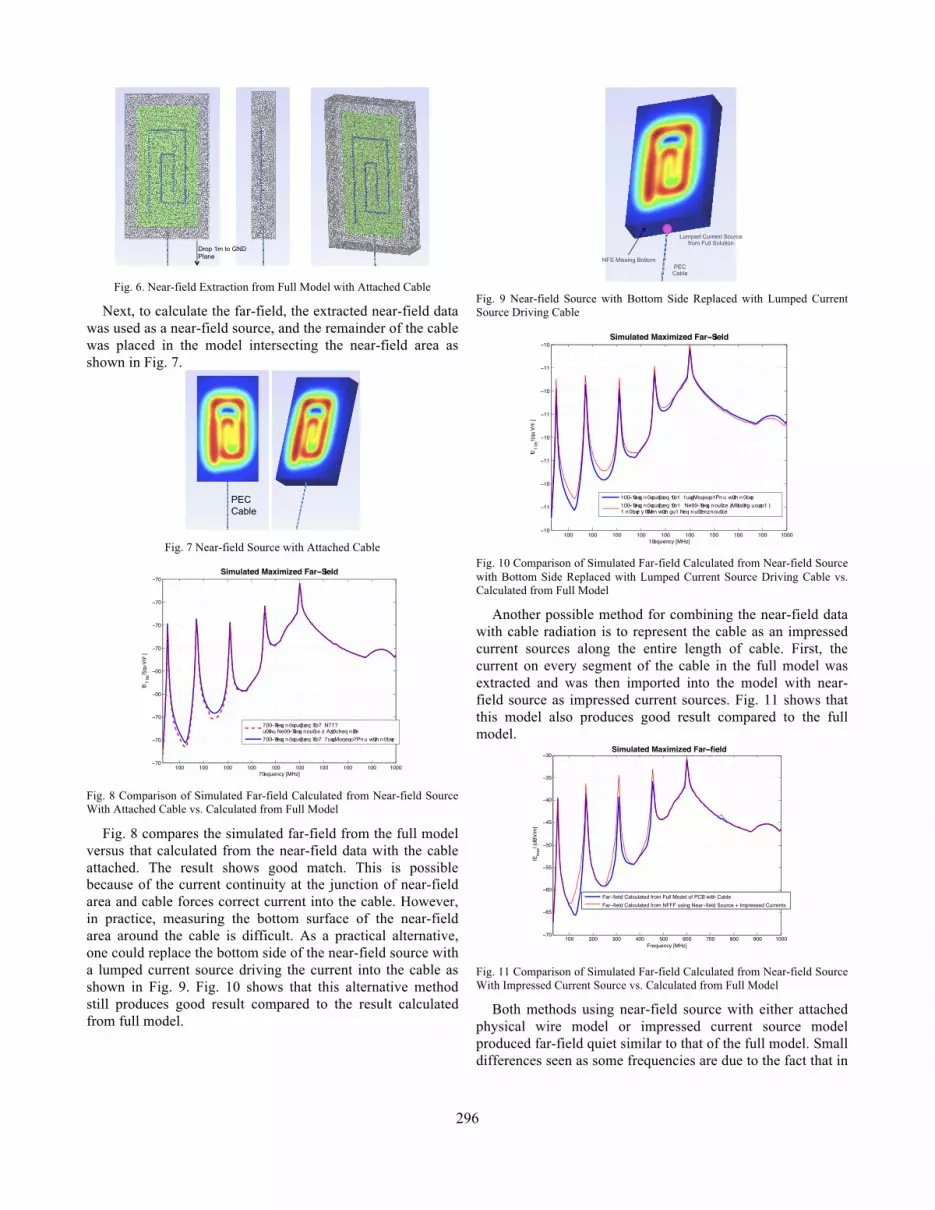
Fig. 6. Near-field Extraction from Full Model with Attached Cable
Next, to calculate the far-field, the extracted near-field data was used as a near-field source, and the remainder of the cable was placed in the model intersecting the near-field area as shown in Fig. 7.
Fig. 7 Near-field Source with Attached Cable
Fig. 8 Comparison of Simulated Far-field Calculated from Near-field Source With Attached Cable vs. Calculated from Full Model
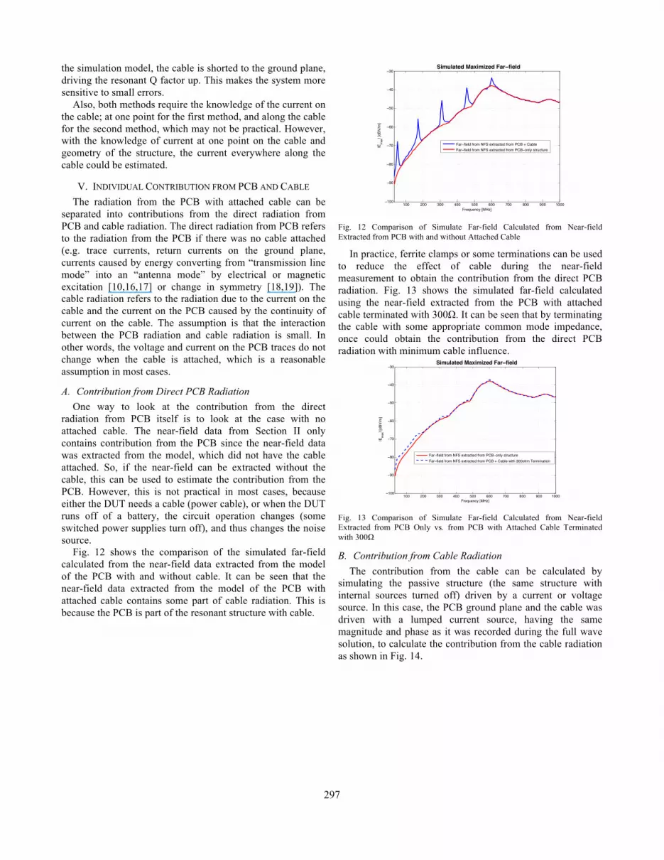
Fig. 8 compares the simulated far-field from the full model versus that calculated from the near-field data with the cable attached. The result shows good match. This is possible because of the current continuity at the junction of near-field area and cable forces correct current into the cable. However, in practice, measuring the bottom surface of the near-field area around the cable is difficult. As a practical alternative, one could replace the bottom side of the near-field source with a lumped current source driving the current into the cable as shown in Fig. 9. Fig. 10 shows that this alternative method still produces good result compared to the result calculated from full model.
Fig. 9 Near-field Source with Bottom Side Replaced with Lumped Current Source Driving Cable
Fig. 10 Comparison of Simulated Far-field Calculated from Near-field Source with Bottom Side Replaced with Lumped Current Source Driving Cable vs. Calculated from Full Model
Another possible method for combining the near-field data with cable radiation is to represent the cable as an impressed current sources along the entire length of cable. First, the current on every segment of the cable in the full model was extracted and was then imported into the model with near-field source as impressed current sources. Fig. 11 shows that this model also produces good result compared to the full model.
Fig. 11 Comparison of Simulated Far-field Calculated from Near-field SourceWith Impressed Current Source vs. Calculated from Full Model
Both methods using near-field source with either attached physical wire model or impressed current source model produced far-field quiet similar to that of the full model. Small differences seen as some frequencies are due to the fact that in
Drop 1m to GND Plane
PEC Cable
��� ��� ��� ��� ��� ��� ��� ��� ��� ������
��
��
��
��
��
��
��
��
���������� ��
���
����
���
���
���������� �������� ���
��� ������ ������������� ������������� ������������������������
��� ������ ������������� ������������� ������ ����
PECCable
Lumped Current Source from Full Solution
NFS Missing Bottom
��� ��� ��� ��� ��� ��� ��� ��� ��� ������
��
��
��
��
��
��
��
��
���������� ��
���
����
���
���
���������� �������� ���
��� ������ ������������� ������������� ������ ����
��� ������ ������������� ���� ������������������������� ��� ���� ������������ ���� ������������
100 200 300 400 500 600 700 800 900 1000−70
−65
−60
−55
−50
−45
−40
−35
−30
Frequency [MHz]
|Em
ax| [
dBV
/m]
Simulated Maximized Far−field
Far−field Calculated from Full Model of PCB with Cable
Far−field Calculated from NFFF using Near−field Source + Impressed Currents
296
the simulation model, the cable is shorted to the ground plane, driving the resonant Q factor up. This makes the system more sensitive to small errors.
Also, both methods require the knowledge of the current on the cable; at one point for the first method, and along the cable for the second method, which may not be practical. However, with the knowledge of current at one point on the cable and geometry of the structure, the current everywhere along the cable could be estimated.
V. INDIVIDUAL CONTRIBUTION FROM PCB AND CABLE
The radiation from the PCB with attached cable can be separated into contributions from the direct radiation from PCB and cable radiation. The direct radiation from PCB refers to the radiation from the PCB if there was no cable attached (e.g. trace currents, return currents on the ground plane,currents caused by energy converting from “transmission line mode” into an “antenna mode” by electrical or magnetic excitation [10,16,17] or change in symmetry [18,19]). The cable radiation refers to the radiation due to the current on the cable and the current on the PCB caused by the continuity of current on the cable. The assumption is that the interaction between the PCB radiation and cable radiation is small. In other words, the voltage and current on the PCB traces do not change when the cable is attached, which is a reasonable assumption in most cases.
A. Contribution from Direct PCB RadiationOne way to look at the contribution from the direct
radiation from PCB itself is to look at the case with noattached cable. The near-field data from Section II only contains contribution from the PCB since the near-field data was extracted from the model, which did not have the cable attached. So, if the near-field can be extracted without the cable, this can be used to estimate the contribution from the PCB. However, this is not practical in most cases, because either the DUT needs a cable (power cable), or when the DUT runs off of a battery, the circuit operation changes (some switched power supplies turn off), and thus changes the noise source.
Fig. 12 shows the comparison of the simulated far-field calculated from the near-field data extracted from the model of the PCB with and without cable. It can be seen that the near-field data extracted from the model of the PCB with attached cable contains some part of cable radiation. This is because the PCB is part of the resonant structure with cable.
Fig. 12 Comparison of Simulate Far-field Calculated from Near-field Extracted from PCB with and without Attached Cable
In practice, ferrite clamps or some terminations can be used to reduce the effect of cable during the near-field measurement to obtain the contribution from the direct PCB radiation. Fig. 13 shows the simulated far-field calculated using the near-field extracted from the PCB with attached cable terminated with 300Ω. It can be seen that by terminating the cable with some appropriate common mode impedance, once could obtain the contribution from the direct PCB radiation with minimum cable influence.
Fig. 13 Comparison of Simulate Far-field Calculated from Near-field Extracted from PCB Only vs. from PCB with Attached Cable Terminated with 300Ω
B. Contribution from Cable RadiationThe contribution from the cable can be calculated by
simulating the passive structure (the same structure with internal sources turned off) driven by a current or voltage source. In this case, the PCB ground plane and the cable was driven with a lumped current source, having the same magnitude and phase as it was recorded during the full wave solution, to calculate the contribution from the cable radiation as shown in Fig. 14.
100 200 300 400 500 600 700 800 900 1000−100
−90
−80
−70
−60
−50
−40
−30
Frequency [MHz]
|Em
ax| [
dBV
/m]
Simulated Maximized Far−field
Far−field from NFS extracted from PCB + Cable
Far−field from NFS extracted from PCB−only structure
100 200 300 400 500 600 700 800 900 1000−100
−90
−80
−70
−60
−50
−40
−30
Frequency [MHz]
|Em
ax| [
dBV
/m]
Simulated Maximized Far−field
Far−field from NFS extracted from PCB−only structure
Far−field from NFS extracted from PCB + Cable with 300ohm Termination
297

Fig. 14 Passive Model Driven with Lumped Current Source
Fig. 15 shows the comparison of the calculated far-field from the passive model versus that from full model. It can be seen that this passive model can predict the cable radiation quiet well.
Fig. 15 Comparison of Simulated Far-field from Passive Model Driven with Lumped Current Source vs. Calculated from Full Model
The passive model requires that we have a good source model (voltage or current source driving the structure). As we mentioned earlier in the paper, if we assume that the geometry does not change between near-field measurement and far-field measurement, then the current on the cable at a particular location can be measured using a current clamp to obtain the current source for the passive model.
C. Combining the Contributions TogetherIn section A, it was shown that by measuring the near-field
without the attached cable or with ferrites/terminations, one could obtain contribution from the direct PCB radiation. In section B, we showed that the contribution of cable radiation could be calculated by simulating a passive structure driven by a proper source model. With an assumption that the interaction between two contributions is small, then we could simply find the sum of the two maximized contributions to estimate the maximum of total radiation. Fig. 16 shows the two individual contributions (top) and comparison of the sumof the two contributions versus the full model solution (bottom).
Fig. 16 Individual Contribution from Direct PCB Radiation and Cable Radiation (top) and Comparison of Sum of Contributions vs. Calculated from Full Model (bottom)
Bottom figure of Fig. 16 shows that the sum of the individual contribution is similar to the actual maximum far-field calculated from the full model.
VI. EXPERIMENTAL RESULTS
A test structure was created to validate the findings from numerical experiments as shown in Fig. 17. The test structure contains a 14×10cm PCB with a microstrip trace routed in some arbitrary directions and terminated on one side with 50Ωresistor. A battery-operated 4MHz comb generator was used to generate a signal feeding the trace from the bottom side. The bottom side of the PCB was shielded with a metallic enclosure to prevent any noise from the comb generator circuit directly being radiated. Thus, only the trace can excite the structure.
Fig. 17 Test Structure
The near-field data (magnitude and phase of tangential E-and H-fields) was obtained for the top surface 8mm above the PCB via time-domain near-field scanning [20]. The scanning resolution was 5mm. The remaining sides were not measured,as the field strengths are weak on these sides and too low for the probe to capture them. At first, the measured near-field data was used to calculate electric fields at 3m horizontal distance when the DUT is placed 1m above an infinite ground plane. The field was maximized over the height of 0.6 – 1.5m, which is the measurable range in our chamber. Fig. 18 shows the comparison of the NFFFT-calculated versus measured electric fields.
PCB GND Plane
PEC Cable
Lumped Current Source from Full Solution
100 200 300 400 500 600 700 800 900 1000−90
−80
−70
−60
−50
−40
−30
Frequency [MHz]
|Em
ax| [
dBV
/m]
Simulated Maximized Far−field
PCB + Cable Connected Full Solution Far−field
PCB + Cable Connected PCB + PC + Lumped Source Far−field
100 200 300 400 500 600 700 800 900 1000−100
−90
−80
−70
−60
−50
−40
−30Simulated Maximized Far−field
|Em
ax| [
dBV
/m]
100 200 300 400 500 600 700 800 900 1000−80
−70
−60
−50
−40
−30
|Em
ax| [
dBV
/m]
Frequency [MHz]
Far−field PCB + Cable from Full Model
Sum of Maximized Individual Contributions
Far−field Calculated from Passive Structure Driven by Current Source
Far−field from NFS extracted from PCB + Cable with 300ohm Termination
298
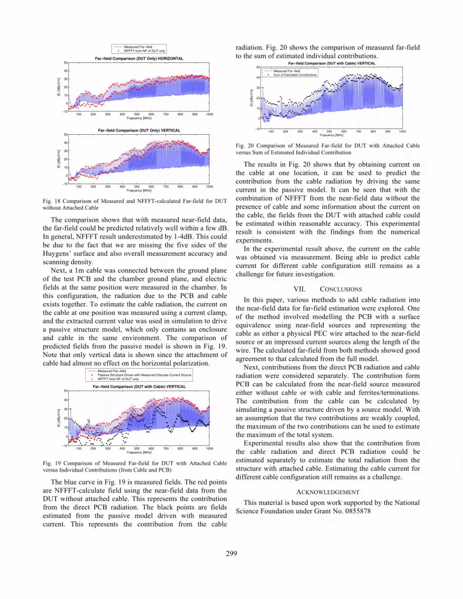
Fig. 18 Comparison of Measured and NFFFT-calculated Far-field for DUT without Attached Cable
The comparison shows that with measured near-field data, the far-field could be predicted relatively well within a few dB. In general, NFFFT result underestimated by 1-4dB. This could be due to the fact that we are missing the five sides of the Huygens’ surface and also overall measurement accuracy and scanning density.
Next, a 1m cable was connected between the ground plane of the test PCB and the chamber ground plane, and electric fields at the same position were measured in the chamber. In this configuration, the radiation due to the PCB and cable exists together. To estimate the cable radiation, the current on the cable at one position was measured using a current clamp, and the extracted current value was used in simulation to drive a passive structure model, which only contains an enclosure and cable in the same environment. The comparison of predicted fields from the passive model is shown in Fig. 19.Note that only vertical data is shown since the attachment of cable had almost no effect on the horizontal polarization.
Fig. 19 Comparison of Measured Far-field for DUT with Attached Cable versus Individual Contributions (from Cable and PCB)
The blue curve in Fig. 19 is measured fields. The red points are NFFFT-calculate field using the near-field data from the DUT without attached cable. This represents the contribution from the direct PCB radiation. The black points are fields estimated from the passive model driven with measured current. This represents the contribution from the cable
radiation. Fig. 20 shows the comparison of measured far-field to the sum of estimated individual contributions.
Fig. 20 Comparison of Measured Far-field for DUT with Attached Cable versus Sum of Estimated Individual Contribution
The results in Fig. 20 shows that by obtaining current on the cable at one location, it can be used to predict the contribution from the cable radiation by driving the same current in the passive model. It can be seen that with the combination of NFFFT from the near-field data without the presence of cable and some information about the current on the cable, the fields from the DUT with attached cable could be estimated within reasonable accuracy. This experimental result is consistent with the findings from the numerical experiments.
In the experimental result above, the current on the cable was obtained via measurement. Being able to predict cable current for different cable configuration still remains as a challenge for future investigation.
VII. CONCLUSIONS
In this paper, various methods to add cable radiation into the near-field data for far-field estimation were explored. One of the method involved modelling the PCB with a surface equivalence using near-field sources and representing the cable as either a physical PEC wire attached to the near-field source or an impressed current sources along the length of the wire. The calculated far-field from both methods showed good agreement to that calculated from the full model.
Next, contributions from the direct PCB radiation and cable radiation were considered separately. The contribution form PCB can be calculated from the near-field source measured either without cable or with cable and ferrites/terminations. The contribution from the cable can be calculated by simulating a passive structure driven by a source model. Withan assumption that the two contributions are weakly coupled, the maximum of the two contributions can be used to estimate the maximum of the total system.
Experimental results also show that the contribution from the cable radiation and direct PCB radiation could be estimated separately to estimate the total radiation from the structure with attached cable. Estimating the cable current for different cable configuration still remains as a challenge.
ACKNOWLEDGEMENT
This material is based upon work supported by the National Science Foundation under Grant No. 0855878
100 200 300 400 500 600 700 800 900 1000−10
0
10
20
30
40
50|E
| [dB
μV
/m]
Frqeuency [MHz]
Far−field Comparison (DUT Only) HORIZONTAL
Measured Far−fieldNFFFT from NF of DUT only
100 200 300 400 500 600 700 800 900 1000−10
0
10
20
30
40
50
Frqeuency [MHz]
|E| [
dBμ
V/m
]
Far−field Comparison (DUT Only) VERTICAL
100 200 300 400 500 600 700 800 900 1000−10
0
10
20
30
40
50
Frqeuency [MHz]
|E| [
dBμ
V/m
]
Far−field Comparison (DUT with Cable) VERTICAL
Measured Far−fieldPassive Structure Driven with Measured Discrete Current SourceNFFFT from NF of DUT only
100 200 300 400 500 600 700 800 900 1000−10
0
10
20
30
40
50
Frqeuency [MHz]
|E| [
dBμ
V/m
]
Far−field Comparison (DUT with Cable) VERTICAL
Measured Far−fieldSum of Estimated Contributions
299

REFERENCES[1] D. Baudry, F. Bicrel, L. Bouchelouk, A. Louis, B. Mazari and P. Eudeline, "Near-field techniques for detecting EMI sources", Electromagnetic Compatibility, 2004 EMC 2004 2004 InternationalSymposium on DOI - 10.1109/ISEMC.2004.1349987,vol. 1, 2004, p. 11-13 vol.1.[2] J. Xiao, D. Liu, D. Pommerenke, W. Huang, P. Shao, X. Li, J. Min and G. Muchaidze, "Near field probe for detecting resonances in EMC application", Electromagnetic Compatibility (APEMC), 2010 Asia-Pacific Symposium on DOI -10.1109/APEMC.2010.5475739, 2010, p. 243-246.[3] P.- Barriere, J.- Laurin and Y. Goussard, "Mapping of Equivalent Currents on High-Speed Digital Printed Circuit Boards Based on Near-Field Measurements", Electromagnetic Compatibility, IEEE Transactions on DOI -10.1109/TEMC.2009.2020297, vol. 51, 2009, p. 649-658.[4] Q. Chen, S. Kato and K. Sawaya, "Estimation of Current Distribution on Multilayer Printed Circuit Board by Near-Field Measurement", Electromagnetic Compatibility, IEEE Transactions on DOI - 10.1109/TEMC.2008.921028, vol. 50, 2008, p. 399-405.[5] D. Baudry, C. Arcambal, A. Louis, B. Mazari and P. Eudeline, "Applications of the Near-Field Techniques in EMC Investigations", Electromagnetic Compatibility, IEEE Transactions on DOI - 10.1109/TEMC.2007.902194, vol. 49, 2007, p. 485-493.[6] R. Laroussi and G.I. Costache, "Far-field predictions from near-field measurements using an exact integral equation solution", Electromagnetic Compatibility, IEEE Transactions on DOI -10.1109/15.305453, vol. 36, 1994, p. 189-195.[7] H. Tazi, F. Bogdanov and T.F. Eibert, "Application of the equivalence principle and the multi excitation approach to method of moments simulations for optimizations of smart entry systems in vehicles", Microwave Conference (EuMC), 2010 European DOI-, 2010, p. 232-235.[8] H.W. Shim and T.H. Hubing, "Derivation of a closed-form approximate expression for the self-capacitance of a printed circuit board trace", Electromagnetic Compatibility, IEEE Transactions on DOI - 10.1109/TEMC.2005.859059, vol. 47, 2005, p. 1004-1008.[9] Y. Kayano, M. Tanaka and H. Inoue, "Radiated emission from a PCB with an attached cable resulting from a nonzero ground plane impedance", Electromagnetic Compatibility, 2005 EMC 2005 2005 International Symposium on DOI -10.1109/ISEMC.2005.1513663, vol. 3, 2005, p. 955-960 Vol. 3.[10] H.-W. Shim and T.H. Hubing, "Model for estimating radiated emissions from a printed circuit board with attached cables due to Voltage-driven sources", Electromagnetic Compatibility, IEEE Transactions on DOI -10.1109/TEMC.2005.859060, vol. 47, 2005, p. 899-907.[11] C. Suriano, J. Suriano and G. Thiele, "A simplified method for predicting common mode current on dipole and monopole structures", Electromagnetic Compatibility, 2005 EMC 2005 2005 International Symposium on DOI - 10.1109/ISEMC.2005.1513558,vol. 2, 2005, p. 457-462 Vol. 2.[12] Y. Kayano, M. Tanaka and H. Inoue, "An equivalent circuit model for predicting EM radiation from a PCB driven by a connected feed cable", Electromagnetic Compatibility, 2006 EMC 2006 2006 IEEE International Symposium on DOI -10.1109/ISEMC.2006.1706285, vol. 1, 2006, p. 166-171.[13] S. Deng, T. Hubing and D. Beetner, "Estimating maximum radiated emissions from printed circuit boards with an attached cable", Electromagnetic Compatibility, IEEE Transactions on, vol. 50, 2008, p. 215-218.[14] EMCoS Ltd., EMCoS EMC Studio, Version 6.0, www.emcos.com[15] C.A. Balanis, Advanced engineering electromagnetics, New York: Wiley, 1989.[16] S. Deng, T.H. Hubing and D.G. Beetner, "Using TEM Cell Measurements to Estimate the Maximum Radiation From PCBs With Cables Due to Magnetic Field Coupling", Electromagnetic
Compatibility, IEEE Transactions on DOI -10.1109/TEMC.2008.919026, vol. 50, 2008, p. 419-423.[17] D.M. Hockanson, J.L. Dreniak, T.H. Hubing, T.P. van Doren, F. Sha and C.-W. Lam, "Quantifying EMI resulting from finite-impedance reference planes", Electromagnetic Compatibility, IEEE Transactions on DOI - 10.1109/15.649814, vol. 39, 1997, p. 286-297.[18] C. Su and T.H. Hubing, "Imbalance Difference Model for Common-Mode Radiation From Printed Circuit Boards", Electromagnetic Compatibility, IEEE Transactions on DOI -10.1109/TEMC.2010.2049853, vol. 53, 2011, p. 150-156.[19] C. Su and T.H. Hubing, "Calculating Radiated Emissions Due to I/O Line Coupling on Printed Circuit Boards Using the Imbalance Difference Method", Electromagnetic Compatibility, IEEE Transactions on DOI - 10.1109/TEMC.2011.2168565, vol. PP, 2011, p. 1-6.[20] Amber Precision Instrument, http://www.amberpi.com
300