normal incidence inas/ingaas dots-in-well detectors with current blocking algaas layer
TRANSCRIPT
Journal of Crystal Growth 251 (2003) 787–793
Normal incidence InAs/InGaAs dots-in-well detectors withcurrent blocking AlGaAs layer
P. Rotellaa, S. Raghavana, A. Stintza, B. Fuchsa, S. Krishnaa,*, C. Morathb,D. Leb, S.W. Kennerlyc
aElectrical and Computer Engineering, Department, Center for High Technology Materials, University of New Mexico,
Albuquerque, NM 87106, USAbAir Force Research Lab (AFRL/VSSS), 3550 Aberdeen Avenue S. E., Building 426, Kirtland Air Force Base, New Mexico 87117, USA
cArmy Research Laboratory, Sensors and Electron Devices Directorate, Adelphi, MD 20783, USA
Abstract
Normal incidence InAs/In0.15Ga0.85As dots-in-a-well detectors operating at T ¼ 78K with lpB7 mm and a broad
spectral width (Dl=l) of 35% are reported. Effect of a current blocking AlGaAs layer on the device performance is
studied. Temperature-dependent dark current, spectral response and calibrated blackbody measurements were
undertaken to determine the responsivity and detectivity of the detectors at 78K. A correction factor was introduced to
include the effect of scattering and reflections in the undoped substrate.
r 2003 Elsevier Science B.V. All rights reserved.
PACS: 81.05.Ea; 81.07.Ta; 81.15.Hi; 85.60.Dw
Keywords: A1. Nanomaterials; A3. Molecular beam epitaxy; A3. Quantum dots; B3. Infrared detectors
1. Introduction
In recent years self-assembled quantum dotinfrared detectors (QDIP) using GaAs basedmaterials have become a very interesting field ofstudy because of their importance to commercialand military applications such as night vision,environmental and chemical monitoring, andthermographic imaging [1–10]. Quantum dotinfrared detectors offer potential advantages overcurrent technologies such as quantum well infrareddetectors, HgCdTe detectors, and other emerging
technologies such as strained superlattice GaSbbased detectors with a Type II band structure.While HgCdTe detectors are the current leaders inhigh performance IR detectors and the strainedlayer superlattice detectors offer potentially lowAuger scattering rates [11], GaAs quantum dotdetectors, which are based on a mature and defect-free technology, could prove beneficial for redu-cing fixed pattern noise in focal plane arrays.
Due to their three-dimensional carrier confine-ment geometry, quantum dot detectors are in-herently sensitive to normally incident radiation.This means that gratings or optocouplers are notnecessary to increase radiation collection and over-come the quantum mechanic selection rules thatprevent normal incidence radiation absorption.
*Corresponding author. Tel.: +505-272-7892; fax: +505-
272-7801.
E-mail address: [email protected] (S. Krishna).
0022-0248/03/$ - see front matter r 2003 Elsevier Science B.V. All rights reserved.
doi:10.1016/S0022-0248(02)02428-4
The normally incident radiation can induce theintersubband transitions in the quantum dotsmaking them more suitable for large area focalplane arrays. The use of quantum dots canovercome the scattering assisted tunneling processthat exists in quantum well detectors, resulting inlower dark current [12]. Another advantage ofusing quantum dots rather than quantum wellbased detectors is the expectation of a largerphotoconductive gain based on a reduced captureprobability [2]. The long intersubband relaxationtime, while also contributing to an increase in darkcurrent, also enhances detection because thephotogenerated carriers remain in the excitedstates for a longer period of time and contributeto a higher photocurrent. Another importantaspect for large area focal plane arrays is theability to tune the spectral response with theapplication of a bias. With the ability to shiftwavelengths adaptive focal plane arrays wouldhave the spectral response of each pixel determinedby an external bias. Bias dependent tunableoperation of QD detectors has recently beendemonstrated [13,14]. However, much more workis necessary to allow QDIP devices to operate athigher temperatures without the use of a coolingsystem. One possible method to help reduce thedark current in these devices is the use of anAlGaAs current blocking layer. In this article, wepresent the effects and results of the addition of thecurrent blocking layer to a quantum dot infrareddetector structure and compare its spectral re-sponse and dark current to the same structurewithout the blocking layer.
2. Growth, fabrication and characterization of
detectors
The quantum dot detectors, VQDIP 1198 and1199, were grown on (1 0 0) undoped GaAssubstrates using a solid source MBE system. TheStranski–Krastanow method was used for theformation of the dot layers. This growth techniquemakes use of the strain between lattice mismatchedsemiconductor materials [15]. The epitaxial filmprefers to minimize its free energy thermodynami-cally and assembles the atoms in three-dimensional
self-assembled islands rather than forming a two-dimensional layer. Typically, these self-assembledquantum dots are pyramidal or lens-like in shape.In this paper, we report quantum dot detectorsthat employ dots-in-a-well structures in whichInAs dots are placed in a thin InGaAs well. Thiswell is in turn placed in a GaAs matrix. Byutilizing the DWELL structure we effectivelylower the ground state of the quantum dot relativeto the bandedge. This provides for better confine-ment of the carriers trapped in the dots and leadsto lower thermionic emission [16]. Another ad-vantage of using the DWELL structure, ascompared to a conventional InAs/GaAs structure,is the higher density of dots which leads to a higherresponsivity.
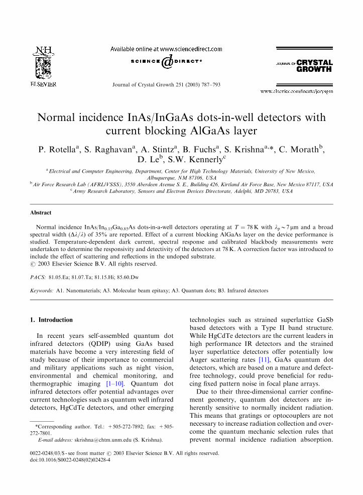
The DWELL structures were grown using aVG-80 solid source molecular beam epitaxy systemwith a cracked As2 source. The VQDIP 1199structure consisted of a 500 nm GaAs buffer, 10periods of the DWELL structure, and a GaAs caplayer for making ohmic contact to the device. TheGaAs layers were grown at a temperature of 5801Cwhile the InGaAs well and the InAs dots weregrown at 4801C. The performance of the quantumdot detectors depends on quantum dot density anddopant concentration [11]. In order to optimize thenumber of dopant atoms per dot, calibrationsamples with different dot doping levels weregrown and the absorption was characterized withPL measurements. From this we learned that theoptimal sheet density for our InAs dots was about1E11/cm2. This corresponds to about 1 to 2electrons per dot. This means that the dopantshould just fill the ground states of the quantumdots and the excited states should be empty.Higher dopant densities result in higher darkcurrent in the detectors. The detector structureswere then grown with 10 layers of n-doped InAs/InGaAs DWELL structures. The heterostructureand the cross-sectional TEM images of theDWELL detectors are shown in Fig. 1.
The n–i–n devices were fabricated into mesadiodes of different aperture sizes using standardlithography, metal evaporation, and wet and dryetching techniques. These devices were designedfor topside illumination and the diameter of theaperture ranged from 25 to 300 mm. Spectral
P. Rotella et al. / Journal of Crystal Growth 251 (2003) 787–793788
measurements were performed using a globarsource within a Thermo-Nicolet 670 spectrometer.The detectors were wire-bonded to a leadless chipcarrier and mounted in a nitrogen cryostat. An off-axis parabolic mirror was used to collect theoutput beam from the FTIR and focus it onto thedetector samples. Dark current measurementswere undertaken at different temperaturesand measured with a HP 4145B semiconductoranalyzer.
3. Results and discussion
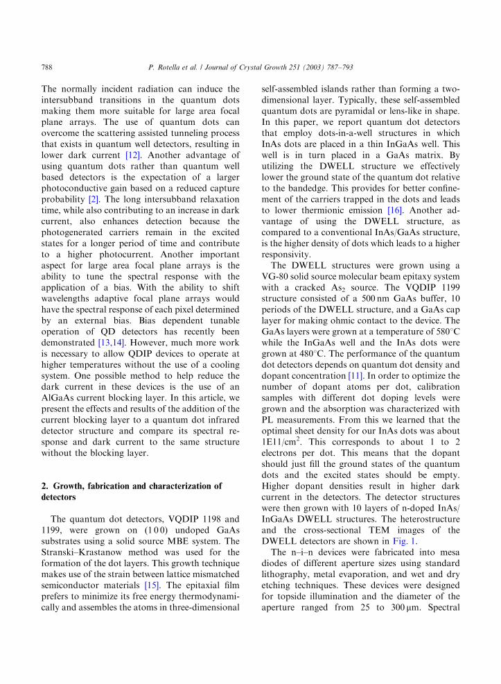
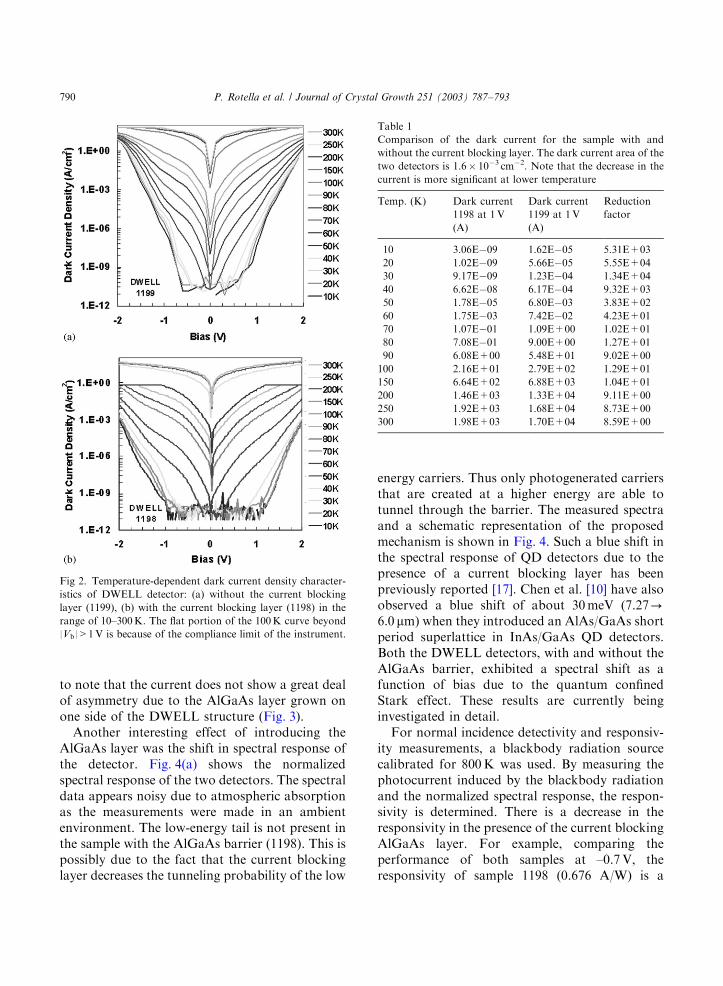
The dark current densities for the two detectorstructures (1198 and 1199) are shown in Fig. 2.Due to the presence of the AlGaAs layer there is asignificant reduction in the dark current in sample1198. There was a reduction in the current densityby an order of magnitude or more depending onthe device temperature. At lower temperatures theeffect is more noticeable (Table 1). It is interesting
(b)
(a)
Fig 1. (a) Heterostructure schematic of the two 10 layer InAs/In0.15Ga0.85As dots in a well (DWELL) detector with and without the
current blocking layer. A cross-sectional transmission electron microscopy image of the detector structure is shown in (b).
P. Rotella et al. / Journal of Crystal Growth 251 (2003) 787–793 789
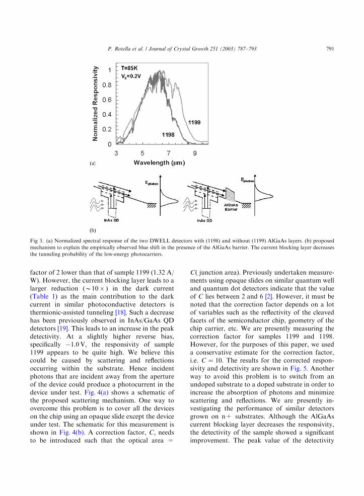
to note that the current does not show a great dealof asymmetry due to the AlGaAs layer grown onone side of the DWELL structure (Fig. 3).
Another interesting effect of introducing theAlGaAs layer was the shift in spectral response ofthe detector. Fig. 4(a) shows the normalizedspectral response of the two detectors. The spectraldata appears noisy due to atmospheric absorptionas the measurements were made in an ambientenvironment. The low-energy tail is not present inthe sample with the AlGaAs barrier (1198). This ispossibly due to the fact that the current blockinglayer decreases the tunneling probability of the low
energy carriers. Thus only photogenerated carriersthat are created at a higher energy are able totunnel through the barrier. The measured spectraand a schematic representation of the proposedmechanism is shown in Fig. 4. Such a blue shift inthe spectral response of QD detectors due to thepresence of a current blocking layer has beenpreviously reported [17]. Chen et al. [10] have alsoobserved a blue shift of about 30meV (7.27-6.0 mm) when they introduced an AlAs/GaAs shortperiod superlattice in InAs/GaAs QD detectors.Both the DWELL detectors, with and without theAlGaAs barrier, exhibited a spectral shift as afunction of bias due to the quantum confinedStark effect. These results are currently beinginvestigated in detail.
For normal incidence detectivity and responsiv-ity measurements, a blackbody radiation sourcecalibrated for 800K was used. By measuring thephotocurrent induced by the blackbody radiationand the normalized spectral response, the respon-sivity is determined. There is a decrease in theresponsivity in the presence of the current blockingAlGaAs layer. For example, comparing theperformance of both samples at –0.7V, theresponsivity of sample 1198 (0.676 A/W) is a
Fig 2. Temperature-dependent dark current density character-
istics of DWELL detector: (a) without the current blocking
layer (1199), (b) with the current blocking layer (1198) in the
range of 10–300K. The flat portion of the 100K curve beyond
|Vb|>1V is because of the compliance limit of the instrument.
Table 1
Comparison of the dark current for the sample with and
without the current blocking layer. The dark current area of the
two detectors is 1.6� 10�3 cm�2. Note that the decrease in the
current is more significant at lower temperature
Temp. (K) Dark current
1198 at 1V
(A)
Dark current
1199 at 1V
(A)
Reduction
factor
10 3.06E�09 1.62E�05 5.31E+03
20 1.02E�09 5.66E�05 5.55E+04
30 9.17E�09 1.23E�04 1.34E+04
40 6.62E�08 6.17E�04 9.32E+03
50 1.78E�05 6.80E�03 3.83E+02
60 1.75E�03 7.42E�02 4.23E+01
70 1.07E�01 1.09E+00 1.02E+01
80 7.08E�01 9.00E+00 1.27E+01
90 6.08E+00 5.48E+01 9.02E+00
100 2.16E+01 2.79E+02 1.29E+01
150 6.64E+02 6.88E+03 1.04E+01
200 1.46E+03 1.33E+04 9.11E+00
250 1.92E+03 1.68E+04 8.73E+00
300 1.98E+03 1.70E+04 8.59E+00
P. Rotella et al. / Journal of Crystal Growth 251 (2003) 787–793790
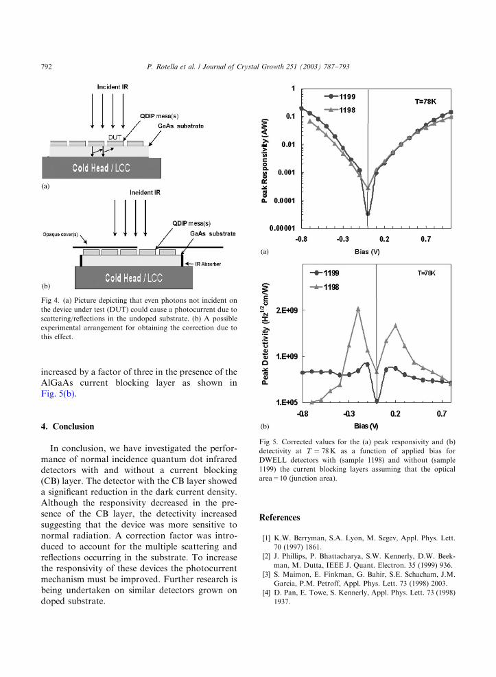
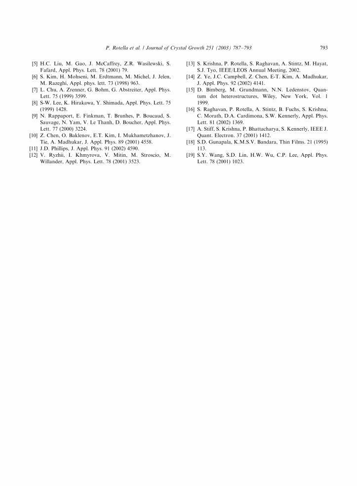
factor of 2 lower than that of sample 1199 (1.32 A/W). However, the current blocking layer leads to alarger reduction (B10� ) in the dark current(Table 1) as the main contribution to the darkcurrent in similar photoconductive detectors isthermionic-assisted tunneling [18]. Such a decreasehas been previously observed in InAs/GaAs QDdetectors [19]. This leads to an increase in the peakdetectivity. At a slightly higher reverse bias,specifically �1.0V, the responsivity of sample1199 appears to be quite high. We believe thiscould be caused by scattering and reflectionsoccurring within the substrate. Hence incidentphotons that are incident away from the apertureof the device could produce a photocurrent in thedevice under test. Fig. 4(a) shows a schematic ofthe proposed scattering mechanism. One way toovercome this problem is to cover all the deviceson the chip using an opaque slide except the deviceunder test. The schematic for this measurement isshown in Fig. 4(b). A correction factor, C; needsto be introduced such that the optical area =
C( junction area). Previously undertaken measure-ments using opaque slides on similar quantum welland quantum dot detectors indicate that the valueof C lies between 2 and 6 [2]. However, it must benoted that the correction factor depends on a lotof variables such as the reflectivity of the cleavedfacets of the semiconductor chip, geometry of thechip carrier, etc. We are presently measuring thecorrection factor for samples 1199 and 1198.However, for the purposes of this paper, we useda conservative estimate for the correction factor,i.e. C ¼ 10: The results for the corrected respon-sivity and detectivity are shown in Fig. 5. Anotherway to avoid this problem is to switch from anundoped substrate to a doped substrate in order toincrease the absorption of photons and minimizescattering and reflections. We are presently in-vestigating the performance of similar detectorsgrown on n+ substrates. Although the AlGaAscurrent blocking layer decreases the responsivity,the detectivity of the sample showed a significantimprovement. The peak value of the detectivity
((a)
(b)
Fig 3. (a) Normalized spectral response of the two DWELL detectors with (1198) and without (1199) AlGaAs layers. (b) proposed
mechanism to explain the empirically observed blue shift in the presence of the AlGaAs barrier. The current blocking layer decreases
the tunneling probability of the low-energy photocarriers.
P. Rotella et al. / Journal of Crystal Growth 251 (2003) 787–793 791
increased by a factor of three in the presence of theAlGaAs current blocking layer as shown inFig. 5(b).
4. Conclusion
In conclusion, we have investigated the perfor-mance of normal incidence quantum dot infrareddetectors with and without a current blocking(CB) layer. The detector with the CB layer showeda significant reduction in the dark current density.Although the responsivity decreased in the pre-sence of the CB layer, the detectivity increasedsuggesting that the device was more sensitive tonormal radiation. A correction factor was intro-duced to account for the multiple scattering andreflections occurring in the substrate. To increasethe responsivity of these devices the photocurrentmechanism must be improved. Further research isbeing undertaken on similar detectors grown ondoped substrate.
References
[1] K.W. Berryman, S.A. Lyon, M. Segev, Appl. Phys. Lett.
70 (1997) 1861.
[2] J. Phillips, P. Bhattacharya, S.W. Kennerly, D.W. Beek-
man, M. Dutta, IEEE J. Quant. Electron. 35 (1999) 936.
[3] S. Maimon, E. Finkman, G. Bahir, S.E. Schacham, J.M.
Garcia, P.M. Petroff, Appl. Phys. Lett. 73 (1998) 2003.
[4] D. Pan, E. Towe, S. Kennerly, Appl. Phys. Lett. 73 (1998)
1937.
Fig 5. Corrected values for the (a) peak responsivity and (b)
detectivity at T ¼ 78K as a function of applied bias for
DWELL detectors with (sample 1198) and without (sample
1199) the current blocking layers assuming that the optical
area=10 (junction area).
Fig 4. (a) Picture depicting that even photons not incident on
the device under test (DUT) could cause a photocurrent due to
scattering/reflections in the undoped substrate. (b) A possible
experimental arrangement for obtaining the correction due to
this effect.
P. Rotella et al. / Journal of Crystal Growth 251 (2003) 787–793792
[5] H.C. Liu, M. Gao, J. McCaffrey, Z.R. Wasilewski, S.
Fafard, Appl. Phys. Lett. 78 (2001) 79.
[6] S. Kim, H. Mohseni, M. Erdtmann, M. Michel, J. Jelen,
M. Razeghi, Appl. phys. lett. 73 (1998) 963.
[7] L. Chu, A. Zrenner, G. Bohm, G. Abstreiter, Appl. Phys.
Lett. 75 (1999) 3599.
[8] S-W. Lee, K. Hirakawa, Y. Shimada, Appl. Phys. Lett. 75
(1999) 1428.
[9] N. Rappaport, E. Finkman, T. Brunhes, P. Boucaud, S.
Sauvage, N. Yam, V. Le Thanh, D. Boucher, Appl. Phys.
Lett. 77 (2000) 3224.
[10] Z. Chen, O. Baklenov, E.T. Kim, I. Mukhametzhanov, J.
Tie, A. Madhukar, J. Appl. Phys. 89 (2001) 4558.
[11] J.D. Phillips, J. Appl. Phys. 91 (2002) 4590.
[12] V. Ryzhii, I. Khmyrova, V. Mitin, M. Stroscio, M.
Willander, Appl. Phys. Lett. 78 (2001) 3523.
[13] S. Krishna, P. Rotella, S. Raghavan, A. Stintz, M. Hayat,
S.J. Tyo, IEEE/LEOS Annual Meeting, 2002.
[14] Z. Ye, J.C. Campbell, Z. Chen, E-T. Kim, A. Madhukar,
J. Appl. Phys. 92 (2002) 4141.
[15] D. Bimberg, M. Grundmann, N.N. Ledenstov, Quan-
tum dot heterostructures, Wiley, New York, Vol. 1
1999.
[16] S. Raghavan, P. Rotella, A. Stintz, B. Fuchs, S. Krishna,
C. Morath, D.A. Cardimona, S.W. Kennerly, Appl. Phys.
Lett. 81 (2002) 1369.
[17] A. Stiff, S. Krishna, P. Bhattacharya, S. Kennerly, IEEE J.
Quant. Electron. 37 (2001) 1412.
[18] S.D. Gunapala, K.M.S.V. Bandara, Thin Films. 21 (1995)
113.
[19] S.Y. Wang, S.D. Lin, H.W. Wu, C.P. Lee, Appl. Phys.
Lett. 78 (2001) 1023.
P. Rotella et al. / Journal of Crystal Growth 251 (2003) 787–793 793