multiple-input-buffer and shared-buffer architectures for optical packet- and burst-switching...
TRANSCRIPT

JOURNAL OF LIGHTWAVE TECHNOLOGY, VOL. 25, NO. 6, JUNE 2007 1379
Multiple-Input-Buffer and Shared-BufferArchitectures for Optical Packet- and
Burst-Switching NetworksKonstantinos Yiannopoulos, Kyriakos G. Vlachos, Member, IEEE, and Emmanouel Varvarigos
Abstract—We present an architecture for implementing opticalbuffers, based on the feed-forward-buffer concept, that can trulyemulate input queuing and accommodate asynchronous packetand burst operation. The architecture uses wavelength convertersand fixed-length delay lines that are combined to form either amultiple-input buffer or a shared buffer. Both architectures aremodular, allowing the expansion of the buffer at a cost that growslogarithmically with the buffer depth, where the cost is measuredin terms of the number of switching elements, and wavelengthconverters are employed. The architectural design also providesa tradeoff between the number of wavelength converters and theirtunability. The buffer architectures proposed are complementedwith scheduling algorithms that can guarantee lossless commu-nication and are evaluated using physical-layer simulations toobtain their performance in terms of bit-error rate and achievablebuffer size.
Index Terms—Input queuing, optical buffers, optical packet andburst switching, programmable delays, wavelength converters.
I. INTRODUCTION
O PTICAL buffering is an important functionality in opticalpacket- and burst-switched (OPS/OBS) networks. It al-
lows the temporary storage of data packets and bursts to resolvecontention at the switch outputs. Various solutions have beenproposed up to date including programmable delay lines [1]–[4]and optoelectronic conversion schemes [5]. Electronic buffer-ing has been extensively utilized in currently installed opticalnetworks; however, it is limited by the electronic processingspeeds and the relatively slow O/E and E/O conversion times.Moreover, the cost and complexity associated with O/E/Oconversions may be alleviated in optical-buffering schemesthrough component miniaturization and integration [6];an integrated optical buffer has been recently reported [7].Optical buffers that are based on programmable delay linesmaintain the advantages of lower energy per written/readbit and smaller power dissipation, as compared to electronicbuffers [8], and have been extensively used to form feed-forward or recirculating architectures employing, in addition,
Manuscript received December 1, 2006; revised February 14, 2007. Thiswork was supported in part by the Operational Program for Educational andVocational Training (EPEAEK), PYTHAGORAS II Program, and in part bythe European Union via the IST/NoE e-Photon/ONe+.
The authors are with the Computer Engineering and Informatics Departmentand with the Research Academic Computer Technology Institute, University ofPatras, 26500 Rio, Greece (e-mail: [email protected]).
Digital Object Identifier 10.1109/JLT.2007.896804
wavelength conversion to enhance buffering capabilities[9], [10]. Most schemes, however, assume slotted operation[1], which requires complex scheduling algorithms and, thus,are not suitable for asynchronous optical packet and burstswitching. In particular, feedback loops theoretically provideinfinite storage time, but they suffer from noise accumulationand optical signal-to-noise-ratio (OSNR) degradation. Further-more, they require that the length of the feedback loop matchesexactly the packet/burst duration in order to avoid loss ofsynchronization and that a large number of them are used tokeep the blocking probability small. In contrast, feed-forwarddelay-line buffers are easier to implement, since the differencein the length of optical paths has to match a segment of thepacket/burst duration (timeslot). Moreover, even though feed-forward delay-line architectures allow for short buffering times,recent studies indicate that statistically multiplexed opticalnetworks will require only minimal buffering [11], providedsome traffic engineering is performed. For these reasons, feed-forward delay-line buffer architectures seem to be a morepractical solution for implementing limited optical buffering inpacket/burst-switched networks.
Within this context, we present in this communication anarchitectural design for optical buffers, based on the feed-forward-buffer concept that can truly emulate input queuingand accommodate asynchronous packet and burst operation.The architectural design uses wavelength converters and fixed-length delay lines to internally route packets and bursts. Theseare combined together to form either a multiple-input bufferdesign, where a separate input buffer is employed per inputport, or a shared-buffer design, where the same optical bufferis shared by all input ports. The latter significantly decreasesthe individual number of fiber delays needed. Both schemesare modular and are engineered to allow for the logarithmicalincrease of the buffer complexity and cost as a function ofthe buffer size. Moreover, as we show later on, the use ofmultiple wavelengths to route internally data bursts signifi-cantly reduces the number of delay stages needed and, thus, thenumber of wavelength converters. The architectural designs arecomplemented with physical-layer simulations to derive theirdesign parameters (achievable buffer size) and illustrate theirefficient performance in terms of bit-error rate (BER). In ouranalysis, we have assumed a wavelength-tuning range of w andinvestigated the cascadability of s stages.
The rest of this paper is organized as follows. Section IIdiscusses the multiple-input-buffer design that consists of
0733-8724/$25.00 © 2007 IEEE
1380 JOURNAL OF LIGHTWAVE TECHNOLOGY, VOL. 25, NO. 6, JUNE 2007
parallel timeslot-interchangers (TSIs) and emulates input queu-ing. The buffer complexity and the number of stages growoptimally (logarithmically) with the buffer depth. Althoughpreviously reported work has also achieved logarithmic growthwith respect to the number of stages [12], [13], we calculatefor the first time to our knowledge the exact dependence of thelogarithm base on the tunability of the wavelength convertersto further reduce the required number of stages. We show thatapproximately 50% of the wavelengths available for internalswitching contribute to this reduction. We also discuss theimplications of deploying the buffer in an OPS/OBS nodeand provide a scheduling/contention-resolution algorithm toachieve lossless communication. In Section III, we present theshared-buffer design that emulates distributed buffering amongall incoming/outgoing links of the optical switch. Similar tothe previous buffer architecture, the number of stages growslogarithmically with buffering time (depth), but distributedbuffering reduces the number of wavelengths that are available.As a result, more stages are required to construct the buffer.Still, the second architecture achieves lossless performance un-der less-strict requirements on the traffic conditions. This paperconcludes with Section IV, which discusses the realization ofthe aforementioned architectural designs and investigates theirefficient error performance versus the number of delay stagesemployed.
II. MULTIPLE-INPUT BUFFER ARCHITECTURE
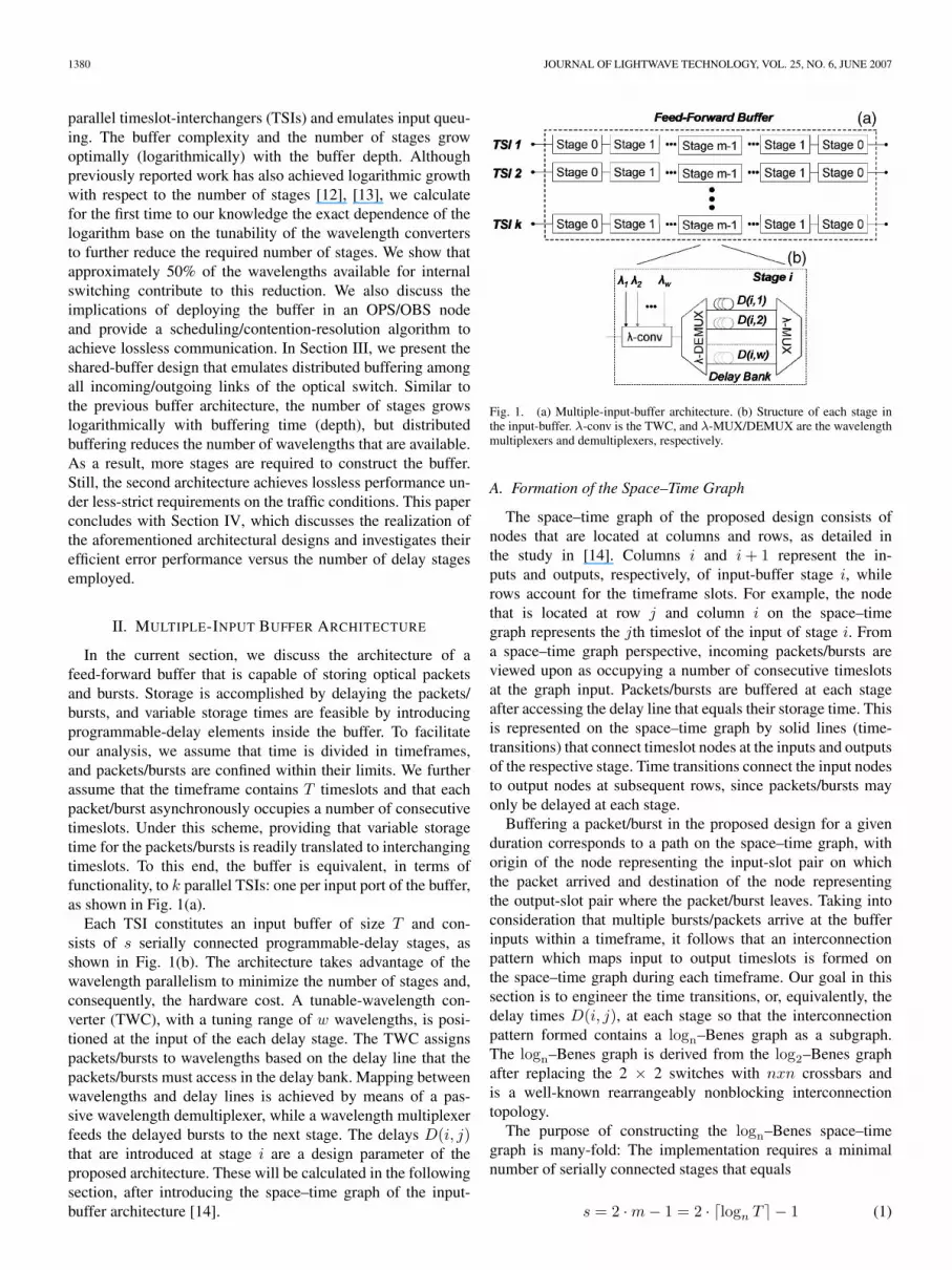
In the current section, we discuss the architecture of afeed-forward buffer that is capable of storing optical packetsand bursts. Storage is accomplished by delaying the packets/bursts, and variable storage times are feasible by introducingprogrammable-delay elements inside the buffer. To facilitateour analysis, we assume that time is divided in timeframes,and packets/bursts are confined within their limits. We furtherassume that the timeframe contains T timeslots and that eachpacket/burst asynchronously occupies a number of consecutivetimeslots. Under this scheme, providing that variable storagetime for the packets/bursts is readily translated to interchangingtimeslots. To this end, the buffer is equivalent, in terms offunctionality, to k parallel TSIs: one per input port of the buffer,as shown in Fig. 1(a).
Each TSI constitutes an input buffer of size T and con-sists of s serially connected programmable-delay stages, asshown in Fig. 1(b). The architecture takes advantage of thewavelength parallelism to minimize the number of stages and,consequently, the hardware cost. A tunable-wavelength con-verter (TWC), with a tuning range of w wavelengths, is posi-tioned at the input of the each delay stage. The TWC assignspackets/bursts to wavelengths based on the delay line that thepackets/bursts must access in the delay bank. Mapping betweenwavelengths and delay lines is achieved by means of a pas-sive wavelength demultiplexer, while a wavelength multiplexerfeeds the delayed bursts to the next stage. The delays D(i, j)that are introduced at stage i are a design parameter of theproposed architecture. These will be calculated in the followingsection, after introducing the space–time graph of the input-buffer architecture [14].
Fig. 1. (a) Multiple-input-buffer architecture. (b) Structure of each stage inthe input-buffer. λ-conv is the TWC, and λ-MUX/DEMUX are the wavelengthmultiplexers and demultiplexers, respectively.
A. Formation of the Space–Time Graph
The space–time graph of the proposed design consists ofnodes that are located at columns and rows, as detailed inthe study in [14]. Columns i and i + 1 represent the in-puts and outputs, respectively, of input-buffer stage i, whilerows account for the timeframe slots. For example, the nodethat is located at row j and column i on the space–timegraph represents the jth timeslot of the input of stage i. Froma space–time graph perspective, incoming packets/bursts areviewed upon as occupying a number of consecutive timeslotsat the graph input. Packets/bursts are buffered at each stageafter accessing the delay line that equals their storage time. Thisis represented on the space–time graph by solid lines (time-transitions) that connect timeslot nodes at the inputs and outputsof the respective stage. Time transitions connect the input nodesto output nodes at subsequent rows, since packets/bursts mayonly be delayed at each stage.
Buffering a packet/burst in the proposed design for a givenduration corresponds to a path on the space–time graph, withorigin of the node representing the input-slot pair on whichthe packet arrived and destination of the node representingthe output-slot pair where the packet/burst leaves. Taking intoconsideration that multiple bursts/packets arrive at the bufferinputs within a timeframe, it follows that an interconnectionpattern which maps input to output timeslots is formed onthe space–time graph during each timeframe. Our goal in thissection is to engineer the time transitions, or, equivalently, thedelay times D(i, j), at each stage so that the interconnectionpattern formed contains a logn–Benes graph as a subgraph.The logn–Benes graph is derived from the log2–Benes graphafter replacing the 2 × 2 switches with nxn crossbars andis a well-known rearrangeably nonblocking interconnectiontopology.
The purpose of constructing the logn–Benes space–timegraph is many-fold: The implementation requires a minimalnumber of serially connected stages that equals
s = 2 · m − 1 = 2 · �logn T � − 1 (1)

YIANNOPOULOS et al.: MULTIPLE-INPUT-BUFFER AND SHARED-BUFFER ARCHITECTURE FOR OPS/OBS NETWORK 1381
Fig. 2. Derivation of the elementary crossbar size on the space–time graph.The number of timeslots that are located at the next stage of the input-bufferand which may be accessed by a timeslot located at the current stage equalsthe number of available wavelengths w. The crossbar that connects timeslotsbetween successive stages is formed so that all input timeslots may access alloutput timeslots.
for a given number T of timeslot per timeframe. Equation(1) shows that by implementing the logn–Benes space–timegraph, one can achieve a drastic reduction in the number ofstages, compared to previously reported [12], [13]. This isof particular importance when considering the hardware costof the implementation. Moreover, as we will show later inSection IV, physical-layer impairments, such as timing jitterand the patterning effect, aggravate the optical-signal qualityas the number of cascaded stages increases. Furthermore, theBenes space–time graph provides optimal (logarithmic) scala-bility with respect to the timeframe size T and is rearrangablynonblocking; thus, the proposed design is capable of storingpackets/bursts without suffering internal collisions. Finally,finding collision-free paths within the Benes graph is a well-studied problem [15].
The building blocks of the logn–Benes graph are nxn cross-bar switches, and thus, the first step for constructing it is todetermine the size of the crossbars. The crossbars are formedout of time transitions on the space–time graph, as shown inFig. 2, which corresponds to the first stage (stage 0) of thebuffer. Input packets/bursts that have arrived within timeslots{1, . . . , n} may all access output timeslots {n, . . . , w}, sincetime transitions to preceding timeslots are not allowed. Thus,the total number of output timeslots that are available to alln input timeslots is limited to w − n + 1. The crossbar inputsequal the crossbar outputs, and we find that the crossbar size is
n = w − n + 1 ⇔ n =⌊
w + 12
⌋(2)
with x denoting the integer part of x. Equation (2) shows thatapproximately 50% of the available wavelengths contribute tothe formation of the crossbars that comprise the logn–Benes.
The second step for constructing the logn–Benes graph is todetermine the time transitions that form the graph’s crossbars inthe respective stages. The process is shown in Fig. 3(a) for thefirst and second stage of the input buffer, as well as in Fig. 3(b)and (c), where the network of Fig. 3(a) is transformed to a
Fig. 3. Formation of the logn–Benes subgraph on the space–time graph. Thenxn virtual switches at stage i are formed out of nodes that lie ni timeslotsapart.
standard representation. The formation of the logn–Benes graphcrossbars requires that at each stage i, time transitions connecttimeslots that are located ni positions apart. This correspondsto setting the switch time delays, in timeslots, equal to
D(i, j) = j · ni, i = 0, . . . ,m − 1, j = 0, . . . , w − 1.(3)
The delays account for all time transitions on the space–timegraph, even though only n time transitions per timeslot nodecontribute to the formation of the virtual crossbars. The re-maining w − n inactive transitions introduce a constant delay,after which, the output timeframe commences [white squares inFig. 3(a)]. At the output of each stage, the delay equals
∆i = ni · (n − 1), i = 0, . . . ,m − 1 (4)
timeslots, and as a result, the minimum total delay that thepackets/bursts experience when traversing the buffer is
∆ =m−1∑i=0
ni · (n − 1) +m−2∑i=0
ni · (n − 1)
=nm + nm−1 − 2
=T +T
n− 2 (5)
timeslots. Equation (5) may be viewed upon as constant storagelatency introduced by the buffer.

1382 JOURNAL OF LIGHTWAVE TECHNOLOGY, VOL. 25, NO. 6, JUNE 2007
Fig. 4. Scheduling algorithm for the multiple-input-buffer architecture.
B. Asynchronous Operation in a Lossless OPS/OBS Node
The multiple-input buffer design provides lossless storage forpackets/bursts that arrive at the incoming links of an OPS/OBSnode within a timeframe T . However, the parallel TSIs do notspatially interconnect, and thus, the design is not capable ofswitching packets/bursts between input and output links of theOPS/OBS node. This shortcoming is addressed by deploying aspace switch between the buffer outputs and the node outgoinglinks. The logn–Benes subgraph of the time–space graph thatrepresents the buffer ensures that there are no collisions insidethe buffer, but still, collisions may occur at the outputs ofthe space switch if two or more packets/bursts simultaneouslyrequire accessing the same output. A scheduling algorithm is,therefore, required at the node control plane to arbitrate poten-tial packet/burst collisions. We illustrate a suitable schedulingalgorithm in Fig. 4. According to the algorithm, the outputframe is partitioned into k successive subframes of equal du-ration. Packets/bursts arriving over incoming link p and head-ing for outgoing link q are scheduled in the output subframe(see Fig. 4)
S ={
q − p + 1, q ≥ pk + p − q + 1, q < p.
(6)
Equation (6) dictates that packets/bursts that head for a par-ticular outgoing link are scheduled to different subframes, de-pending on the link on which they arrive. As such, packet/burstcollisions are avoided, provided that the total duration ofpackets/bursts dpq (measured in timeslots) that arrive over linkp and heading for outgoing link q does not exceed the subframe
dpq ≤ T
k, 1 ≤ p, q ≤ k. (7)
Equations (6) and (7) provide an algorithm for schedulingpackets/bursts without losses. Following the discussion ofSection II-A, packets/bursts are scheduled after being convertedto the appropriate internal wavelength and accessing the respec-tive delay line at each programmable-delay stage. As a result,scheduling requires that the state of wavelength converters have
Fig. 5. Routing in the logn–Benes network.
to be set prior to sending the packets/bursts to the buffer. From aspace–time graph perspective, (6) defines the timeslot patternsat the input and the output stages of the logn–Benes network forone timeframe. Thus, setting the internal wavelengths is equiv-alent to calculating the state of the crossbars in all intermediatestages of the logn–Benes graph so that the input timeslot patternis routed to the respective output.
To perform routing in a logn–Benes graph, we proposeto use a modified parallel-routing algorithm that extends theparallel-routing algorithm on a binary Benes graph [15]. Thealgorithm involves setting the state of the outermost crossbars(at stages 0 and s−1) of the Benes graph, given the respectivetimeslot patterns. The outermost crossbars are then omitted,and the remaining network is partitioned into multiple Benesgraphs of reduced size. The algorithm is recursively applied onthe resulting graphs until the state of all crossbars is set. Anexample of the routing algorithm is detailed in the followingsection.
C. Benes Routing in the logn–Benes Network
A routing example for the logn–Benes network is illustratedin Fig. 5 for n = 3 and T = 9. The timeslots at the input of thebuffer (stage 0) are assigned successive n-ary values, and therespective input permutation vector is formed. The permutationvector that corresponds to the output of the buffer (stage s−1) is

YIANNOPOULOS et al.: MULTIPLE-INPUT-BUFFER AND SHARED-BUFFER ARCHITECTURE FOR OPS/OBS NETWORK 1383
formed in a similar fashion, after taking into account the resultsof the scheduling algorithm. In the example of Fig. 5, the inputand output permutation vectors are
πin = (00 01 02 10 11 12 20 21 22)
πout = (02 21 22 20 00 11 01 10 12). (8)
We first focus on the input permutation vector. After exitingstage 0 on the space–time graph, the input permutation vectorbecomes
π0 = (0a8 0a7 0a6 1a5 1a4 1a3 2a2 2a1 2a0).(9)
Equation (9) corresponds to time transitions with ai denotingthe output nodes that have been accessed. In a similar fashion,the output permutation vector at the input of stage s is
π2 = (0b2 2b7 2b8 2b6 0b0 1b4 0b1 1b3 1b5)(10)
with bi referring to the input nodes that have been accessedby the inverse time transitions. In (10), bi are assigned to rowsaccording the output permutation vector, due to the symmetryof the logn–Benes graph [15]. Moreover, the symmetry of thenetwork implies that ai and bi that are located in a commonrow are equal, and as a result, T equations that correlate ai
and bi are derived. The equations are solved after taking intoconsideration that ai (and bi) satisfy
am·n+i = am·n+j , i = j, i, j ∈ {0, 1, . . . , n − 1} (11)
so that no collisions occur inside the crossbars. The solution tothe equations for the example of Fig. 5 is evaluated as
π0 =(02 01 00 12 10 11 21 20 22)
π2 =(02 21 20 22 00 11 01 10 12). (12)
After solving the equations for the outermost stages of thelogn–Benes graph, we remove the aforementioned stages anddivide the remaining graph into three (n in general) subgraphs.The permutation vectors of each subgraph are derived from(12) after grouping together the vector elements that correspondto the same subgraph or, equivalently, have a common leastsignificant symbol
π0in = (0 1 2) → π0
out = (2 0 1)
π1in = (0 1 2) → π1
out = (2 1 0)
π2in = (0 1 2) → π2
out = (0 2 1). (13)
No further permutation vectors have to be evaluated for thespecific example, since the permutation vectors of (12) and (13)suffice to define the state of the crossbars at all stages.
The state of the crossbars at each stage l is set after takinginto account the least significant symbols of the input andoutput permutation vectors that correspond to stage l. We
assume that the aforementioned symbols form the reducedpermutations vectors ρin
l and ρoutl ; for instance, these are
ρin0 = (0 1 2 0 1 2 0 1 2)
ρout0 = (2 1 0 2 0 1 1 0 2) (14)
for stage 0 in our example. It is straightforward to verify fromFig. 3(a) that routing inside the logn–Benes graph correspondsto setting the delays at each stage equal to
dl = ∆l +(ρout
l − ρinl
) · nl, 0 ≤ l < s (15)
where ∆i is given by (4). This is equivalent to setting thewavelengths of the respective wavelength converters equal to
wl = n + ρoutl − ρin
l , 0 ≤ l < s. (16)
An advantage of the parallel-Benes-routing algorithm re-lies on its low complexity, which leads to small executiontimes when the algorithm is implemented in hardware. Aninitial implementation of the algorithm on Xilinx Virtex-IIFPGAs for w = 3 and T = 16 achieved execution time equalto 100 ns. This result is comparable to the duration of aframe of length T = 10 slots, where each slot carries a singleasynchronous transfer mode cell at 40 Gb/s (10.6 ns).
III. SHARED-BUFFER ARCHITECTURE
In the previous section, we discussed a buffering architecturethat involves deploying one buffer per input. The architectureis optimal as far as the number of delay stages is concerned,but it requires the data traffic that arrives at the buffer to beequally distributed among its inputs, according to (6). In thecurrent section, we discuss a shared-buffer architecture that re-quires less strict traffic conditions for lossless operation. Sharedbuffering is achieved by dedicating a number of wavelengthsto spatially interconnect the parallel TSIs of the multiple-input-buffer design. The new design is shown in Fig. 6(a) andconsists of serially interconnected programmable-delay stagesin which the delay bank is accessible to all input ports, asdetailed in Fig. 6(b). At each delay stage, k parallel wavelengthconverters assign the incoming packets/bursts to wavelengthsthat correspond to a pair of delay lines and output ports. Thedelay lines and output ports are accessed by the packets/burststhrough all-passive space switches. Similar to Section II, ourgoal is to engineer the delays D(i, j) that must be introducedat each stage so that the resulting space–time graph contains aBenes interconnection network as a subgraph.
A. Formation of the Space–Time Graph
The space–time graph for the first stage (stage 0) of theshared-buffer architecture is illustrated in Fig. 7. In contrast tothe space–time graph of the multiple-input-buffer architecture,each timeslot node in the space–time graph of the currentarchitecture includes k separate space nodes that correspondto the delay-stage inputs and outputs, as illustrated at the inset

1384 JOURNAL OF LIGHTWAVE TECHNOLOGY, VOL. 25, NO. 6, JUNE 2007
Fig. 6. (a) Shared-buffer architecture. (b) At the respective stages, eachwavelength is assigned to a pair of delays and output ports. The normalizedwavelength tunability wa is defined as the ratio of the available wavelengths wto the number of input/output ports k.
Fig. 7. Derivation of the elementary crossbar on the space–time graph. Eachnode of the space–time graph representing timeslots is expanded to k separatenodes that correspond to the input/output ports. The number of timeslots thatare located at the next stage of the buffer and may be accessed by a timeslotlocated at the current stage equals the number of available wavelengths wdivided by the number of ports k. The virtual switch that connects timeslotsbetween successive stages is formed so that all input timeslots may access alloutput timeslots.
of Fig. 7. All transitions between the input and output spacenodes of a delay stage are valid within a timeslot, since allstage outputs may be accessed by any stage input in Fig. 6(b).Time transitions are limited to nodes located at following rows,following the discussion of Section II-A.
For the rest of this section, we only consider time tran-sitions and timeslot nodes that form the Benes subgraphon the space–time graph to simplify the illustration of ouranalysis. However, the time transitions between input andoutput timeslot nodes include all k possible space transitionsbetween the corresponding input and output space nodes. Thisapproach results in constructing the Benes interconnectionnetwork on the time transitions of the space–time graph and,
Fig. 8. (a), (b) Formation of the logd–Benes subgraph on the time transitionsof the space–time graph. The dxd virtual switches at stage i are formed out ofnodes that lie di timeslots apart. (c) Expanded interconnection network.
afterward, expanding the crossbars and connections of theresulting network by a factor of k. Within this context, ourgoal is to engineer a logd–Benes interconnection network onthe time transitions of the space–time graph that correspondsto the shared-buffer architecture. The procedure is illustrated inFigs. 7 and 8. We first determine the size d of the elementarycrossbars that comprise the Benes graph, and then, we definethe delays that are required to form the logd–Benes graph onthe space–time graph. The crossbar size is determined aftercalculating the number wa of timeslots that are fully accessedat the output of the stage 0 on the space–time graph. This isequal to the wavelength tunability w normalized by the numberof ports k
wa =⌊w
k
⌋. (17)
The size of the crossbars is calculated after combining(2) and (17)
d =⌊
wa + 12
⌋=
⌊⌊wk
⌋+ 1
2
⌋. (18)
The logd–Benes graph is formed as in Fig. 8(a) and (b) bysetting the delays equal to
D(i, j) = j · di, i = 0, . . . ,m − 1, j = 0, . . . , wa − 1.(19)

YIANNOPOULOS et al.: MULTIPLE-INPUT-BUFFER AND SHARED-BUFFER ARCHITECTURE FOR OPS/OBS NETWORK 1385
Fig. 9. Scheduling algorithm for the shared-buffer architecture.
Similar to the multiple-input-buffer design, only d time tran-sitions are utilized per timeslot, and as a result, the burstsexperience a minimum storage latency equal to
∆ =m−1∑i=0
di · (d − 1) +m−2∑i=0
di · (d − 1)
= dm + dm−1 − 2
= T +T
d− 2 (20)
timeslots.The fully expanded network that includes space transitions
is detailed in Fig. 8(c) after taking into consideration that eachtime transition includes k space transitions and that the crossbarsize is n = k · d nodes in total. The fully expanded networkis rearrangably nonblocking, and thus, buffering without in-ternal collisions can be achieved. Moreover, the number ofdelay stages that are required to implement the shared-bufferarchitecture is given by (see Fig. 8)
s = 2 · m − 1 = 2 · �logd T � − 1. (21)
Equation (21) shows that the shared-buffer design is not optimalas compared to the multiple-input-buffer design, and this isbecause we have constructed a logd–Benes graph on the timetransitions instead of logn–Benes graphs on both time andspace transitions. As a result, the scalability of the sharedbuffer with respect to the timeframe T is suboptimal. Moreover,the shared-buffer design does not scale with the number ofinput/output ports, and additional ports may only be accom-modated if redundant wavelengths are provisioned. However,the drawbacks of the shared-buffer architecture are balanced bythe fact that it requires less-strict-traffic conditions to achievelossless operation, as we will show in the following section.
B. Asynchronous Operation in a Lossless OPS/OBS Node
The shared-buffering architecture may be deployed as-is inan OPS/OBS node, since buffering and switching are performedindependently. Moreover, the rearrangable nonblocking prop-
erty of the expanded interconnection graph of Fig. 8(c) ensuresthat no packet/burst collisions take place inside the sharedbuffer, provided that the total traffic that arrives at all bufferinputs and heads for a specific buffer output does not exceed Ttimeslots within a timeframe. This is a looser traffic conditionthan (6), since incoming traffic does not have to be equallydistributed among all buffer inputs.
Packets/bursts that arrive within the same timeframe areplaced on a common outgoing frame, which starts after ∆timeslots following the end the incoming frame. In the shared-buffer architecture, output timeslots are occupied by incomingpackets/bursts according to a modification of the packing rulethat is detailed in the study in [13]. The modified packing ruleis illustrated in Fig. 9. Packets/bursts that head for a commonoutgoing link and, thus, the respective timeslots they occupy,are logically grouped together, and the timeslots that belong tothe same group are given ranks. A rank of a timeslot equalsrq, if it is the rth timeslot that has arrived at incoming link pand heads for outgoing link q. A timeslot at the incoming time-frame with rank rq will be mapped at the output timeframe totimeslot
yq =p−1∑l=1
nl,q + rq − 1, y ∈ {0, . . . , T − 1} (22)
where nl,q is the total duration of packets/bursts (in timeslots)between incoming link l and outgoing link q.
The modified packing rule determines the storage time ofeach packet/burst inside the buffer. Moreover, each packet/burstrequests that it be switched to an outgoing node link. Follow-ing the discussion of Section III-A, both storing and switch-ing of packets/bursts are implemented by properly assigningwavelengths inside the programmable-delay stages. From aspace–time graph perspective, storing and switching form theinput/output permutation patterns of the Benes network, whilewavelength assignment is equivalent to setting the state of thenetwork crossbars. To this end, we developed a parallel-Benes-routing algorithm suitable for the expanded logd–Benes graphof Fig. 8. An indicative example of the algorithm is detailed inthe following section.

1386 JOURNAL OF LIGHTWAVE TECHNOLOGY, VOL. 25, NO. 6, JUNE 2007
Fig. 10. Routing in the expanded logd–Benes graph.
C. Benes Routing for the logd–Benes Network
An example for routing in the logd–Benes graph is detailedin Fig. 10 for n = 4 (k = 2, d = 2) and T = 4. The input andoutput permutation vectors are given by
πin =(00 01 02 03 10 11 12 13)πout =(00 01 03 11 02 10 12 13). (23)
The permutation vectors at the output of stage 0 and the inputof stage s−1 are calculated as
π0 = (0a0 0a1 0a2 0a3 1a4 1a5 1a6 1a7)π2 = (0b0 0b1 0b3 1b5 0b2 1b4 1b6 1b7). (24)
Equation (24) is solved for ai and bi using the symmetryproperties of the expanded logn–Benes graph, after taking intoaccount (11). The solution is facilitated, however, by the factthat crossbars are connected with groups of k-parallel lines inthe expanded network. As a result, ai (and bi) that correspondto the same k parallel-line group may be interchanged, sincethey originate from and head for the same crossbar. Thus
am·n+i ↔ am·n+j , i = j, i, j ∈ {0, 1, . . . , k − 1}.(25)
A solution for the outermost stages in our example is
π0 =(00 01 02 03 13 12 11 10)π2 =(00 01 02 13 03 12 11 10). (26)
We then omit the outermost crossbars and divide the resultinggraph into two (d in general) subgraphs. The permutationvectors for the subgraphs are formed after grouping togetherthe vector elements that correspond to the same crossbar. Thisis equivalent to grouping vector elements which have the leastsignificant symbols z that satisfy
z ∈ [i · k, (i + 1) · k − 1] , 0 ≤ i < d. (27)
In the example of Fig. 10, we find that
π0in = (00 01 11 10)→π0
out = (00 01 11 10)π1
in = (02 03 13 12)→π1out = (02 13 03 12). (28)
Equation (28) is readily solved after renumbering the vectorelements with respect to the column they occupy
π0in = (0 1 3 2) → π0
out = (0 1 3 2)π1
in = (0 1 3 2) → π1out = (0 3 1 2). (29)
Equations (26) and (29) suffice to calculate the permutationvectors ρin
l and ρoutl at all network stages and define the cross-
bars’ state. The respective wavelengths are assigned accordingto (16).
IV. SEMICONDUCTOR-OPTICAL-AMPLIFIER-BASED
MACH–ZEHNDER INTERFEROMETER
(SOA-MZI)-BASED IMPLEMENTATION
In the current section, we discuss the realization of theproposed buffer architectures with SOA-MZI TWCs. The primetarget is to investigate the BER degradation that is imposed byeach SOA-MZI TWC stage, with a goal to determine the maxi-mum number of stages s that may be cascaded. Even thoughSOA-MZI TWCs are not format transparent, like the four-wave-mixing-based TWCs [16], they are well-suited candidatesfor the proposed multistage designs, since they require lowswitching energies and provide high output powers. Therefore,it is possible to directly cascade delay stages without deployinginline booster amplifiers that aggravate the OSNR and limit theTWCs cacadability.
We have used a common simulation setup for both buffersarchitectures, as shown in Fig. 11, since both architecturesinvolve the cascaded operation of programmable-delay stages.The fiber delay lines were not taken into account during thesimulations, since their lengths are application specific and aredetermined by the available wavelengths and the time-framesize, according to (3) and (19). Moreover, the delay line lossesare negligible in comparison with the Mux/Demux losses formost practical cases.
The cascadability of SOA-MZI TWCs has been investigatedat 10 and 40 Gb/s using the VPI Transmission Maker simulationsoftware. The simulation parameters are summarized in Table I,and the simulation setup is shown in Fig. 11 for both rates. Asymmetric MZI topology has been considered for all TWCs,with two identical SOAs residing at the MZI arms. The SOAsof the setup have been modeled using the built-in VPI TLLMmodel [17] with parameters that have been experimentally ver-ified [18]. The SOA-generated amplified spontaneous emissionhas also been taken into account in the TLLM parameters.A 3-dB optical coupler at the input of the MZIs splits theincoming signal into two components that induce gain andphase changes in the respective SOAs. The SOA gain and phasechanges are imparted on two replicas of a continuous-wave(CW) signal that operates at a wavelength. The CW signalreplicas interfere in a 3-dB coupler at the output of the MZI,and the MZI switch state is set to ON or OFF, depending onthe whether the CW signal replicas have experienced differentgains and phases or not. Differential operation of the switch isaccomplished by introducing attenuation and temporal delay inthe lower MZI arm input-signal component. Under this scheme,

YIANNOPOULOS et al.: MULTIPLE-INPUT-BUFFER AND SHARED-BUFFER ARCHITECTURE FOR OPS/OBS NETWORK 1387
Fig. 11. (Top) Simulation setup of the SOA-MZI TWC. Att: Optical Attenuator. ODL: Optical Delay Line. CW: Continuous Wave. (Bottom) Simulated BERversus receiver power for the cascaded SOA-MZI wavelength converters operating at (a) 10 and (b) 40 Gb/s. The eye diagrams of the signals at the input of thebuffer and at buffer stages 1 and 7 are shown as insets.
TABLE ISIMULATION PARAMETERS
the upper arm component switches the MZI ON, and the lowerarm component switches the MZI OFF [19]. A copropagatinginput/CW configuration with ideal additional combiners andsplitters has been considered for the MZIs to avoid the excessivegain overshooting and slow recovery in the SOAs [20]. Inlineoptical attenuators of constant attenuation are deployed at theoutput of the TWCs so that all stages exhibit unity gain, andthe limited input dynamic range of the MZI TWCs does notaffect the setup performance. In an actual implementation, theinline optical attenuators would account for the losses ofthe multiplexers, demultiplexers, and delay lines that constructthe programmable delay stages of both buffer designs. Theattenuators are replaced by optical amplifiers when the bufferstages exhibit excessive loss, using the integrated TWC topol-ogy that has been demonstrated in the study in [21].
The simulation setup has been tested with a 231 − 1 pseudo-random bit sequence encoded on Gaussian optical pulses. Theinput signal was corrupted by additive white Gaussian noisebefore entering the first stage of the setup. The simulationresults are presented in Fig. 11(a) and (b) for line rates of10 and 40 Gb/s, respectively. Fig. 11(a) illustrates the BER
performance versus the received power for up to seven cascadedTWCs. A negative power penalty of up to 2 dB has beenobserved for all stages due to the regenerative properties of theMZI TWC [22]. Higher received powers are required to achieveerror-free operation of the simulated setup, as compared topreviously reported experimental results, owing to the highlevel of the input noise spectral density. The corresponding eyediagrams reveal that signal quality degrades with the numberof cascaded stages, since amplitude variations in the incomingpulse train result in timing variations at the output of theTWC, thus causing accumulation of timing jitter. The samenumber of stages has also been achieved at 40 Gb/s at theexpense of a 1.5-dB power penalty, as shown in Fig. 11(b).Still, the signal quality is worse, as compared with that ofthe 10-Gb/s operation, and it can be verified from the eyediagrams at 40 Gb/s. Signal quality is degraded due to timingjitter that is accumulated with the number of stages and thepatterning effect that is introduced by the limited gain-recoverytime of the SOA. Despite the fact that the SOAs are driven athigher currents to provide for a faster gain-recovery time, thelarge pulsewidth of the 40-Gb/s signals does not allow for alarger gain-recovery time span. Shorter pulsewidths, however,would require a smaller delay between the signal componentsthat enter the MZI; thus, the TWCs would exhibit loss, andamplification would be necessary between stages. The signal-degradation effects of wavelength crosstalk between the CWand input signals have not been taken into account, sincevery low crosstalk values have been demonstrated in similarSOA-MZI setups [20]. Moreover, the extinction ratio of theSOA-MZI has been considered ideal [23]. We believe that bothassumptions are valid, since our buffer designs require only alimited number of cascaded stages.
Following the analysis of the simulation results, we mayconclude that the maximum number of delay stages for theaforementioned buffer designs that yield an efficient BER of

1388 JOURNAL OF LIGHTWAVE TECHNOLOGY, VOL. 25, NO. 6, JUNE 2007
less than 10−9 is seven. For more stages, the simulationsrevealed that the accumulated timing jitter and pattern effect de-grade error performance to less than 10−7. Still, seven stages arewell capable of providing storage times of practical use whenaccompanied by broad wavelength-tuning range w, accordingto (1) and (21). For instance, for five available wavelengths,the seven-stage multiple-input buffer is capable of storing 81packets, with sufficient buffering capability (according to [11]).Equal storage time may be achieved for a two-port shared-buffer architecture, at the expense of 11 wavelengths. Thetuning range of the SOA-MZI TWCs is determined by thechannel spacing and the spectral width of the SOA gain peak,which is typically about 25 nm. Wide TWCs operating at40 Gb/s have been recently demonstrated [21].
The simulation results of the current section have beenrecently utilized toward the experimental demonstration of a10-Gb/s multiple-input buffer [24]. The experimental demon-stration of the proposed buffer architecture has been performedfor three wavelengths (w = 3) and three stages (s = 3), and thebuffer has achieved error-free buffering of four optical packetsat 10 Gb/s.
V. CONCLUSION
We have presented the architectural design of two opticalburst buffers using wavelength converters and fixed-lengthdelay lines that are combined to form either a multiple-inputbuffer or a shared buffer. Both schemes are modular, allow-ing the expansion of the buffer at a cost that grows loga-rithmically with the buffer size, where the cost is measuredin terms of the number of switching elements (wavelengthconverters) required, while wavelength parallelism is used tosignificantly reduce the number of delay stages. Furthermore,we have also proposed architecture-suited algorithms for pro-viding contention resolution within the buffering time, as wellas algorithms for scheduling the internal wavelengths, againfor contention resolution. The architectural study was comple-mented with physical-layer simulation of cascaded wavelengthconverters at 10 and 40 Gb/s to investigate the efficient errorperformance of the proposed buffer designs. It was found thaterror-free operation at power penalties below 0 and 1.5 dB,respectively, can be achieved for up to seven cascaded wave-length converters.
REFERENCES
[1] D. K. Hunter, M. C. Chia, and I. Andonovic, “Buffering in optical packetswitches,” J. Lightw. Technol., vol. 16, no. 12, pp. 2081–2094, Dec. 1998.
[2] I. Chlamtac et al., “CORD: Contention resolution by delay lines,” IEEEJ. Sel. Areas Commun., vol. 14, no. 5, pp. 1014–1029, Jun. 1996.
[3] C. Guillemot et al., “Transparent optical packet switching: The EuropeanACTS KEOPS project approach,” J. Lightw. Technol., vol. 16, no. 12,pp. 2117–2134, Dec. 1998.
[4] R. L. Cruz and J.-T. Tsai, “COD: Alternative architectures for high-speedpacket switching,” IEEE/ACM Trans. Netw., vol. 4, no. 1, pp. 11–21,Feb. 1996.
[5] S. Bjørnstad, N. Stol, and D. R. Hjelme, “An optical packet switch designwith shared electronic buffering and low bit rate add/drop inputs,” in Proc.Int. Conf. Transparent Opt. Netw., 2002, pp. 69–72.
[6] R. V. Caenegem et al., “From IP over WDM to all-optical packet switch-ing: Economical view,” J. Lightw. Technol., vol. 24, no. 4, pp. 1638–1645,Apr. 2006.
[7] E. F. Burmeister and J. E. Bowers, “Integrated gate matrix switch foroptical packet buffering,” IEEE Photon. Technol. Lett., vol. 18, no. 1,pp. 103–105, Jan. 2006.
[8] R. S. Tucker, “The role of optics and electronics in high-capacity routers,”J. Lightw. Technol., vol. 24, no. 12, pp. 4655–4673, Dec. 2006.
[9] M. C. Chia et al., “Packet loss and delay performance of feedback andfeed-forward arrayed-waveguide gratings-based optical packet switcheswith WDM inputs-outputs,” J. Lightw. Technol., vol. 19, no. 9, pp. 1241–1254, Sep. 2001.
[10] C. M. Gauger, “Dimensioning of FDL buffers for optical burst switchingnodes,” in Proc. 6th IFIP Work. Conf. ONDM, Torino, Italy, Feb. 2002,pp. 117–132.
[11] M. Enachescu, Y. Ganjali, A. Goel, N. McKeown, andT. Roughgarden, “Routers with very small buffers,” in Proc. IEEEINFOCOM, 2006, pp. 1–11.
[12] D. K. Hunter, W. D. Cornwell, T. H. Gilfedder, A. Franzen, andI. Andonovic, “SLOB: A switch with large optical buffers for packetswitching,” J. Lightw. Technol., vol. 16, no. 10, pp. 1725–1736, Oct. 1998.
[13] E. A. Varvarigos, “The ‘packing’ and the ‘scheduling’ packet switcharchitectures for almost all-optical lossless networks,” J. Lightw. Technol.,vol. 16, no. 10, pp. 1757–1767, Oct. 1998.
[14] D. K. Hunter and D. G. Smith, “New architectures for optical TDMswitching,” J. Lightw. Technol., vol. 11, no. 3, pp. 495–511, Mar. 1993.
[15] T. T. Lee and S. Y. Liew, “Parallel routing algorithms in Benes–Closnetworks,” IEEE Trans. Commun., vol. 50, no. 11, pp. 1841–1847,Nov. 2002.
[16] N. Chi and S. Yu, “Optical subcarrier labeling transparent to the payloadformat using carrier suppression technique,” IEEE Photon. Technol. Lett.,vol. 18, no. 8, pp. 971–973, Apr. 15, 2006.
[17] VPI ComponentMaker, Active Photonics User’s Manual. Ch. 5: Overviewof the TLLM.
[18] E. Kehayas et al., “ARTEMIS: 40-Gb/s all-optical self-routing node andnetwork architecture employing asynchronous bit and packet-level opticalsignal processing,” J. Lightw. Technol., vol. 24, no. 8, pp. 2967–2977,Aug. 2006.
[19] K. Tajima, “All-optical switch with switch-off time unrestricted by car-rier lifetime,” Jpn. J. Appl. Phys., vol. 32, no. 12A, pp. L1746–L1749,Dec. 1, 1993.
[20] J. Leuthold et al., “All-optical Mach–Zehnder interferometer wavelengthconverters and switches with integrated data- and control-signal sep-aration scheme,” J. Lightw. Technol., vol. 17, no. 6, pp. 1056–1066,Jun. 1999.
[21] V. Lal et al., “Performance optimization of an InP-based widely tunableall-optical wavelength converter operating at 40 Gb/s,” IEEE Photon.Technol. Lett., vol. 18, no. 4, pp. 577–579, Feb. 15, 2006.
[22] J. Mork, F. Ohman, and S. Bischoff, “Analytical expression for the biterror rate of cascaded all-optical regenerators,” IEEE Photon. Technol.Lett., vol. 15, no. 10, pp. 1479–1481, Oct. 2003.
[23] J. Leuthold et al., “All-optical space switches with gain and principallyideal extinction ratios,” IEEE J. Quantum Electron., vol. 34, no. 4,pp. 622–633, Apr. 1998.
[24] O. Zouraraki et al., “Optical packet buffering in all-optical time-slot-interchanger architecture,” IEEE Photon. Technol. Lett. submitted forpublication.
Konstantinos Yiannopoulos was born in Tripoli, Arcadia, Greece, inDecember 1977. He received the Ph.D. and Diploma degrees in electricaland computer engineering from the National Technical University of Athens,Athens, Greece, in 2004 and 2000, respectively.
From 1999 to 2004, he was with the Photonics Communications ResearchLaboratory, National Technical University of Athens. He is currently a PostDoctoral Researcher with the Computer Engineering and Informatics De-partment, University of Patras, Rio, Greece. His research related experienceincludes high-speed all-optical logic, optical-signal processing for packet- andburst-switched networks, and high-rate optical sources. He is the Author orCoauthor of more than ten papers in IEEE journals and sponsored conferences.
Dr. Yiannopoulos is a member of the IEEE Lasers and Electro-Optics Society(LEOS) and the IEEE Communications Society. He was one of the recipientsof the IEEE LEOS Graduate Student Fellowship Award in 2004.
YIANNOPOULOS et al.: MULTIPLE-INPUT-BUFFER AND SHARED-BUFFER ARCHITECTURE FOR OPS/OBS NETWORK 1389
Kyriakos G. Vlachos (S’00–M’02) received the Dipl.-Ing. degree in electricaland computer engineering and the Ph.D. degree in electrical and computerengineering from the National Technical University of Athens (NTUA), Athens,Greece, in 1998 and 2001, respectively.
From 1997 to 2001, he was a Senior Research Associate with the PhotonicsCommunications Research Laboratory (ICCS/NTUA). In April 2001, he waswith Bell Laboratories, Lucent Technologies, working on behalf of the AppliedPhotonics Group. Since 2005, he has been a Faculty Member with the ComputerEngineering and Informatics Department, University of Patras, Rio, Greece.His research interests are in the areas of high-speed protocols and technologiesfor broadband high-speed networks, optical packet/burst switching, and gridnetworks. He has participated in various research projects funded by theEuropean Commission (IST-STOLAS, IST-PRO3, ESPRIT-DOALL, e-photon/ONe+, and IST-PHOSPHOROUS). He is the (Co)Author of more than70 journal and conference publications and is the holder of five patents.
Prof. Vlachos is a member of the Technical Chamber of Greece.
Emmanouel Varvarigos was born in Athens, Greece, in 1965. He received theDiploma in electrical and computer engineering from the National TechnicalUniversity of Athens in 1988 and the M.S. and Ph.D. degrees in electrical engi-neering and computer science from the Massachusetts Institute of Technology,Cambridge, in 1990 and 1992, respectively.
He has held faculty positions at the University of California, Santa Barbara,from 1992 to 1998, as an Assistant Professor and, later, an Associate Professor,and Delft University of Technology, Delft, The Netherlands, from 1998 to2000, as an Associate Professor. In 2000, he became a Professor with theDepartment of Computer Engineering and Informatics, University of Patras,Rio, Greece, where he is currently heading the Communication Networks Lab-oratory. He is also the Director of the Network Technologies Sector, ResearchAcademic Computer Technology Institute, which, through its involvementin pioneering research and development projects, has a major role in thedevelopment of network technologies and telematic services in Greece.