moving towards high carrier mobility power devices in
TRANSCRIPT
Moving Towards High Carrier MobilityPower Devices in Silicon and Silicon
Carbide
Inauguraldissertation
zur
Erlangung der Würde eines Doktors der Philosophie
vorgelegt der
Philosophisch–Naturwissenschaftlichen Fakultät
der Universität Basel
von
Dipl.-Ing. Harald R. Rossmann
aus Wien (Österreich)
Basel, Juli 2016
Original document stored on the publication server of the University of Basel http://edoc.unibas.ch
This work is licensed under agreement "Attribution Non-Commercial No Derivatives – 2.5 Switzer-land". The complete text may be viewed here: http://creativecommons.org/licenses/by-nc-nd/2.5/ch/deed.en.


iii
Genehmigt von der Philosophisch-Naturwissenschaftlichen Fakultät auf Antrag von:
Prof. Dr. Thomas A. Jung
Prof. Dr. Martino Poggio
Basel, am 21. Juni 2016
Prof. Dr. Jörg Schibler
Dekan

iv
“We choose to go to the moon. We chooseto go to the moon in this decade and dothe other things, not because they areeasy, but because they are hard, becausethat goal will serve to organize and mea-sure the best of our energies and skills,because that challenge is one that we arewilling to accept, one we are unwillingto postpone, and one which we intend towin, and the others, too.”
John F. Kennedy
Abstract
This thesis reports on recent progress regarding the characterization, design and fabri-cation of modern power semiconductor devices in Silicon (Si) as well as in the promisingwide band gap material Silicon Carbide (SiC). Up to now, state of the art power devicesare architectured on the basis of monocrystalline Si-wafers. This is due to the highmaterial quality of Si in combination with the availability of a mature and reliable fabri-cation technology based on a well-established process library. However, more and moresophisticated device designs such as e.g. the Super-Junction (SJ) architecture requirean increasing number of fabrication steps therefore increasing the amount of possiblesources of error. Further, more complex three-dimensional dopant distribution profilesare needed for the devices to withstand the high blocking voltage demands of currentpower semiconductor applications when operated in reverse direction. This dopant dis-tribution has to be monitored, at least for control samples, after implantation, afterfurther thermal processes and during the duty cycle. To ensure reliable device opera-tion, in particular for charge compensated devices, this monitoring or mapping has tobe performed locally with high precision and sensitivity.
In this work complementary Scanning Probe Microscopy (SPM) based methods like:Kelvin Probe Force Microscopy (KPFM), Scanning Capacitance Force Microscopy (SCFM)and Scanning Spreading Resistance Microscopy (SSRM) have been explored for a precisemonitoring of carrier concentration profiles. This is due to the fact that so far none of theestablished industrial techniques such as e.g. Secondary Ion Mass Spectrometry (SIMS)or Spreading Resistance Probe (SRP) was mature enough to simultaneously full-fill allthe major requirements of the semiconductor industry in terms of spatial resolution,sensitivity, reproducibility and the ability to quantify dopant concentrations. Further,SIMS is probing the chemical composition rather than the charge carrier distribution.To ‘look inside’ the inhomogeneously doped sample, smooth device cross-sections need
v
vi Abstract
to be prepared in a reliable manner and without distorting the ‘as implanted/activated’dopant profile. In this way artefacts arising from a topographic signal can be ruled out.For Si the easiest way would be to cleave the wafer along a certain crystallographic direc-tion. However, since the SPM methods presented here shall serve as a characterizationtool with a general validity another approach that is also suitable for different crystalstructures and materials with a hardness close to diamond had to be found. For thisreason a chemical mechanical polishing (CMP) procedure had been developed at PSI.This process was optimized for maintaining a low surface state density as it is importantto avoid a complete pinning of the Fermi level for the KPFM measurements. The sub-sequent Atomic Force Microscopy (AFM) imaging has been performed in collaborationwith the experts in the research group of Prof. Ernst Meyer at the University of Basel.
Within this project it has been demonstrated that every SPM derived method is capa-ble to qualitatively map carrier concentrations down to an unprecedented low regime.However, a difference regarding the lateral resolution was observed which can be un-derstood by different information depths depending on the underlying physical quantityto be measured together with an imperfect surface preparation which is leading to anaccumulation or depletion of defects at the surface. The most critical technique in thatsense - due to its high surface sensitivity - is the contact potential difference measure-ment that is utilized by KPFM to draw conclusions on the carrier concentration. Bylaser illumination of the sample during the KPFM experiment a Surface Photo Voltage(SPV) occurs in a surface near layer with a thickness in the order of the minority carrierdiffusion length. Thus, the surface sensitivity is reduced and the signal distortion due tothe unfavourable influence of surface defects gets less pronounced. Even though SCFMis also based on the detection of the electrostatic force that develops between the tip andthe sample, this method is less affected by the surface because it is probing a differentphysical quantity, namely the total capacitance of the rather extended oxide/depletionlayer capacitance system. Furthermore, the magnitude of the SCFM signal scales inverseproportionally with respect to the carrier concentration, hence this method is theoret-ically offering the highest sensitivity in the low concentration regime. Nevertheless, aquantification scheme for this technique is still in development and further work on lo-cally acquired spectroscopic capacitance-voltage (C-V ) measurements is needed towardsa reliable quantification procedure. The third SPM derived method SSRM, is operatedin contact mode under high normal forces to ensure that the spreading resistance isthe dominant resistance contribution for the current flowing between the tip and thesample. Under these circumstances the local carrier concentration and its impact on themagnitude and the sign of the output current can be investigated in a very accurate andquantitative manner. Beside that, the high mechanical forces cause an abrasive motionof the tip while scanning the sample. This feature is beneficial in two ways: on one handthe native oxide and the underlying defect-rich surface layer are removed while on the

vii
other hand a phase transformation of a tiny sample volume just below the tip occurswhich locally decreases the resistivity and increases the spatial resolution. Hence, theSSRM technique is showing a high degree of reproducibility and is therefore ideal forquantitative studies.
As mentioned above the considerable complexity of the fabrication process and thelimited material properties of Si in terms of a high critical electric field and a highthermal conductivity accelerated the search for novel substrates for power semiconductorapplications. Beside offering an order of magnitude higher critical electric field due to itswide band gap (WBG), SiC also attracted attention since it can be thermally oxidizedresulting in a silicon dioxide (SiO2) layer as its native oxide. Therefore, this materialhas been classified as most promising and theoretical improvements of a - by a factorof 400 - lower ON-resistance have been calculated. However, to date SiC devices arefacing other problems related to the engineering of dopant profiles and the more complexnature of the oxidation process which limit their performance and hinder their large-scalecommercialization.
The incorporation of a specific dopant distribution in SiC is most effectively done by anion implantation process followed by a high temperature annealing step which is neededto restore the crystal structure after implantation-induced damage and to electronicallyactivate the dopant atoms. This is caused by the fact that in SiC due to its wideband gap of 2.4-3.2 eV (depending on its poly-type) basically no dopant diffusion atreasonable thermal budgets occurs. Notably, not all of these dopant atoms are ionizedand contribute to the electric conduction within the semiconductor. Especially thehole concentration p and the acceptor concentration NA can differ significantly in SiCdue to the large ionization energies. Hence it has to be taken into account that thefinal performance of a SiC power device might be inferior to the expected performancefrom the implantation parameters. This behaviour is in clear contrast to Si where atroom temperature basically all donor and acceptor atoms are ionized and no furtherdifferentiation between the dopant and the carrier (electronically active dopant) profilehas to be made. The above mentioned SPM methods are sensitive to the carrier ratherthan to the dopant profile and within this work it has been demonstrated that e.g.the p-doped guard ring structure of a SiC Schottky diode which is shielding the metalcontact from high electric fields that occur under reverse bias operation can be resolved.
Another challenge for SiC Metal Oxide Semiconductor Field Effect Transistor (MOS-FET) devices are low carrier mobilities inside the thin conducting channel at the semi-conductor/oxide interface and threshold voltage instabilities. Due to the more complexnature of the oxidation process which requires the removal of carbon atoms in the formof CO or CO2 from the SiC crystal the SiC/SiO2 interface is showing a high densityof interface trap states that act as scattering centres and degrade the carrier mobility.Hence, experimentally observed charge carrier mobilities are by a factor of 10 below

viii Abstract
the theoretical value of the bulk material. Thereby the ON-resistance which is inverseproportional to the mobility is increased which is leading to a higher amount of powerdissipation in the ON-state of the device. Unsurprisingly, a lot of research effort hasbeen triggered in this direction resulting in breakthrough called post-oxidation anneal-ing (POA) under gaseous ambients. Nitrogen and phosphorous based chemistries haveshown a passivating effect on the density of interface trap states. However, the origin ofthis mechanism is not yet fully understood. A possible explanation is a counter-dopingeffect within a thin layer at the semiconductor surface.
A second - maybe easier - pathway to increase the channel mobility is the utilization ofthe crystal anisotropy. The mobility strongly depends on the orientation of the channelwith respect to the crystallographic axis. Among them the 1120 direction exhibits thehighest mobility. In the here presented project this approach has been utilized to improvethe device performance without changing too many parameters regarding the oxidationor post-oxidation treatments at the same time. In this case the remaining challenge wasto develop an etching process which is able to etch several µm deep trenches into SiC andto precisely control the shape of the resulting trench profile. It has been demonstratedthat sharp corners that would cause field crowding at the edges can be eliminated bythe usage of very small DC biases applied between the electrode of the plasma chamberand the substrate. Furthermore, the steepness of the sidewalls could be controlled bythe composition of the plasma gas flows. Contrary to previous reports we found thatthe addition of oxygen to the dry etching process is not helping to avoid microtrenching.Either a pure SF6 based process or an SF6 based process with the addition of Ar haveshown the best results. With this success a full manufacturing cycle for a nanoscaletrench MOSFET has been designed.


This dissertation is dedicated to my mother for her ongoing love and support andto the memory of my beloved father who could not see this thesis completed.

Preface
The research area of solid state physics is offering an interesting playground forexperimental physicists since many different disciplines within this superordinatefield that are in a constant interplay with each other have to be taken into accountfor a precise description of nature in terms of “the study of matter, energy and theinteraction between them” as it is stated in one of the definitions of physics.Within the scope of this thesis the concepts of surface science and semiconduc-tor physics and manufacturing have been brought together to overcome certainchallenges of state of the art power semiconductor devices. Didactically the frameof this work embraces fundamental solid state physics, semiconductor device en-gineering and the - from a textbook perspective - existing gap between them tobe directed towards a broader audience even without the requirement of a toospecific background knowledge in either of these fields.The content itself will be organized in a chronological order according to the dif-ferent research projects that have been conducted during my PhD time at thePaul Scherrer Institute. In other words, after giving an introduction to the ex-isting challenges and to the methods used for characterization, the thesis willbe split into two parts. The first one adresses the imaging and the analysis ofelectronically active dopant profiles also including sample preparation routineswhile the second one covers the design and the different processing steps towardsnovel prototype trench MOSFET devices in SiC. As part of the “Nano-Argovia”programme of the Swiss Nanoscience Institute (SNI) both topics have been inves-tigated in close collaboration together with the University of Basel as academicand ABB as industrial partner. For the second project experts from the CSEMMuttenz complemented our research consortium.
xi


Contents
Abstract v
Preface xi
List of Abbreviations xvii
1 Introduction to modern power semiconductor devices 1
1.1 Historical overview . . . . . . . . . . . . . . . . . . . . . . . . . . . . . . 1
1.1.1 Physical concepts . . . . . . . . . . . . . . . . . . . . . . . . . . . 2
1.1.2 Evolution of semiconductor devices and substrates . . . . . . . . 5
1.1.3 Compound semiconductors beyond Silicon . . . . . . . . . . . . . 7
1.2 Power devices and their power electronic applications . . . . . . . . . . . 11
1.2.1 Semiconductor power devices as building blocks for power conver-sion systems . . . . . . . . . . . . . . . . . . . . . . . . . . . . . . 11
1.2.2 Applications . . . . . . . . . . . . . . . . . . . . . . . . . . . . . . 16
2 Experimental techniques and processes 19
2.1 Cross-section preparation . . . . . . . . . . . . . . . . . . . . . . . . . . 19
2.1.1 Chemical-mechanical polishing . . . . . . . . . . . . . . . . . . . 19
2.2 SPM-based characterization methods . . . . . . . . . . . . . . . . . . . . 23
2.2.1 Kelvin Probe Force Microscopy . . . . . . . . . . . . . . . . . . . 24
xiii

xiv CONTENTS
2.2.2 Scanning Capacitance Force Microscopy . . . . . . . . . . . . . . 26
2.2.3 Scanning Spreading Resistance Microscopy . . . . . . . . . . . . 28
2.3 Trench MOSFET fabrication and mobility measurements . . . . . . . . . 30
2.3.1 Ion implantation . . . . . . . . . . . . . . . . . . . . . . . . . . . 31
2.3.2 Inductively coupled plasma reactive ion etching of trenches . . . 31
2.3.3 Oxidation process . . . . . . . . . . . . . . . . . . . . . . . . . . 34
2.3.4 Polycrystalline Si filling and metal contacts . . . . . . . . . . . . 36
2.3.5 Assessment of channel mobilities . . . . . . . . . . . . . . . . . . 37
3 Low dopant regime carrier profiling by SPM methods 39
3.1 Quantitative analysis of ultra-lightly doped Si Super-Junction structuresby complementary two-dimensional carrier profiling techniques implementedin a Scanning Probe Microscope . . . . . . . . . . . . . . . . . . . . . . . 40
3.1.1 Super-Junction device architecture . . . . . . . . . . . . . . . . . 40
3.1.2 In-depth comparison . . . . . . . . . . . . . . . . . . . . . . . . . 41
3.1.3 Conclusions . . . . . . . . . . . . . . . . . . . . . . . . . . . . . . 44
3.2 Quantitative dopant imaging, spectroscopy and space charge region ob-servation by SSRM on semiconductor device cross-sections . . . . . . . . 46
3.2.1 Analysis of the space charge region . . . . . . . . . . . . . . . . . 47
3.2.2 Quantification by means of the Arora mobility model . . . . . . . 49
3.2.3 Local I-V characterization . . . . . . . . . . . . . . . . . . . . . . 51
3.2.4 Conclusions . . . . . . . . . . . . . . . . . . . . . . . . . . . . . . 53
4 Characterization of active device areas in 4H-SiC 55
4.1 Two-dimensional carrier profiling on lightly doped n-type 4H-SiC epitax-ially grown layers . . . . . . . . . . . . . . . . . . . . . . . . . . . . . . . 56
4.1.1 Epitaxial growth . . . . . . . . . . . . . . . . . . . . . . . . . . . 56
4.1.2 C-V characterization . . . . . . . . . . . . . . . . . . . . . . . . . 57
4.1.3 SPM-Based two-dimensional carrier profiling . . . . . . . . . . . 58
4.1.4 Conclusions . . . . . . . . . . . . . . . . . . . . . . . . . . . . . . 60
4.2 Junction Barrier Schottky (JBS) Rectifier Interface Engineering Facili-tated by Two-Dimensional (2D) Dopant Imaging . . . . . . . . . . . . . 62
4.2.1 JBS device design . . . . . . . . . . . . . . . . . . . . . . . . . . 62

CONTENTS xv
4.2.2 Fabrication . . . . . . . . . . . . . . . . . . . . . . . . . . . . . . 63
4.2.3 Two-dimensional dopant imaging . . . . . . . . . . . . . . . . . . 64
4.2.4 Conclusions . . . . . . . . . . . . . . . . . . . . . . . . . . . . . . 66
5 On the assessment of channel mobilities in 4H-SiC trench MOSFETs 67
5.1 Device simulations on novel high channel mobility 4H-SiC trench MOS-FETs and their fabrication processes . . . . . . . . . . . . . . . . . . . . 68
5.1.1 Device performance simulations . . . . . . . . . . . . . . . . . . . 69
5.1.2 Dry-etching of trenched MOS-controlled FETs . . . . . . . . . . . 72
5.1.3 Conclusions . . . . . . . . . . . . . . . . . . . . . . . . . . . . . . 73
6 Summary and outlook 75
6.1 Achievements . . . . . . . . . . . . . . . . . . . . . . . . . . . . . . . . . 76
6.2 Ongoing and future work . . . . . . . . . . . . . . . . . . . . . . . . . . . 79
Bibliography 81
Acknowledgments 95
Publication list 97
Curriculum Vitae 103


List of Abbreviations
The following table contains an alphabetically ordered list of abbreviations used through-out this thesis:
Methods
AFM Atomic Force MicroscopyCMP Chemical Mechanical PolishingC-V Capacitance-VoltageICP Inductively Coupled PlasmaI-V Current-VoltageKPFM Kelvin Probe Force MicroscopyMP Mechanical Polishingnc non-contactPOA Post Oxidation AnnealingRIE Reactive Ion EtchingSCFM Scanning Capacitance Force MicroscopySEM Scanning Electron MicroscopeSEPC Secondary Electron Potential ContrastSIMS Secondary Ion Mass SpectrometrySPM Scanning Probe MicroscopySPV Surface Photo VoltageSRP Spreading Resistance ProbeSSRM Scanning Spreading Resistance MicroscopyTCAD Technology Computer Aided Design
xvii

xviii List of Abbreviations
Devices
AC Alternating CurrentBG Buried GridBJT Bipolar Junction TransistorDC Direct CurrentGTO Gate Turn Off ThyristorIGBT Insulated Gate Bipolar TransistorJBS Junction Barrier SchottkyMISFET Metal Insulator Semiconductor Field Effect TransistorMOSFET Metal Oxide Semiconductor Field Effect TransistorSBD Schottky Barrier DiodeSCR Space Charge RegionSJ Super Junction
Materials
Al AluminumAl2O3 Aluminium oxideCr ChromiumGaAs Gallium arsenideGaN Gallium nitrideGe GermaniumInP Indium phosphidePMMA PolymethylmethacrylatNi NickelSi SiliconSiC Silicon carbideSiO2 Silicon dioxide
CHAPTER 1
Introduction to modern power semiconductor devices
1.1 Historical overview
The rich and complex history of semiconductor physics among many other disciplines isfar away from following a straight line in its development and progress [1–3]. It rathertook many unexpected turns. In one case the term ‘renaissance’ is even used [1] which isdue to the fact that early stage semiconductor detectors couldn’t compete with vacuumelectron tubes in terms of reliability. Later on however, semiconductors outperformedthermionic valves in many application sectors because technological obstacles were over-come which enabled a more reliable operation. Another nice example of the sometimesdifficult to predict turns of technological evolution is given by a quote that dates backto the year 1943 and is attributed to Thomas J. Watson Sr., who was the founder andthen CEO of IBM:
“I think there is a world market for about five computers.”
Notably, there is no other company that later on contributed so much to the successfulintegration of personal computers into people’s homes than IBM. Unsurprisingly numer-ous challenges from the physical understanding towards device applications still neededto be overcome until the former statement by Mr. Watson was eventually falsified andthe new era of the so called “Silicon age” began.Before discussing which material fits which application best, the discovery of fundamen-tal semiconducting properties needed to be well understood. Even though the devel-opment of first semiconductor devices took place - from a chronological point of view -often in parallel, in the following paragraphs they are described separately.
1

2 Chapter 1. Introduction to modern power semiconductor devices
1.1.1 Physical concepts
The three most fundamental properties attributed to semiconductors are:
1. an increasing conductivity with temperature
2. a light induced photo-conductivity
and
3. a conductivity which depends on the presence of impurities/dopants
ad 1)The term materials of semiconducting nature, dates back to the work of A. Volta in1782 [4], who observed that the discharge speed of an electro-meter depends on thenature of the material brought in contact with it. The discovery however, of one ofthe characteristic properties of semiconductors, namely the increase of the conductivityat higher temperatures, is attributed to M. Faraday [5] in 1833. He recognized thatthe conducting power of silver sulfide (Ag2S) or the ‘sulphuret of silver’ as he called itwas increased when the temperature is increased. This behaviour was contrary to thatprimarily observed for metals [6].In the original publication [5] he described this effect as follows:
“When a piece of this sulphuret, half an inch in thickness, was put between surfacesof platina, terminating the poles of a voltaic battery of twenty pairs of four-inch plates, agalvanometer being also included in the circuit, the needle was slightly deflected, indicat-ing a feeble conducting power. On pressing the platina poles and the sulphuret togetherwith the fingers, the conducting power increased and the whole became warm.”
Further, he found that this effect was enhanced by putting a lamp in close proximity tothe Ag2S and the conductivity of this material became similar to those of metals. Thiseffect was reversible and under ideal conditions (good contact with the platina poles,freshly charged battery, initial temperature not too low) the Joule heating of the currentwas enough to provoke this behaviour.However, the underlying mechanism kept researchers puzzling for several decades. Onlya better understanding of the transport properties of charged particles in terms of theirresulting electrical and heat current [7] together with the discovery of the electron byJ.J. Thomson [8] in 1897 opened up a pathway for the theoretical formalism by theDrude-model [9] of the free electron gas. In this model the electrons can move freely inanalogy to gas molecules inside an ideal gas. The success of this model in describingthe empirically found ratio between the thermal and the electrical conductivity that

1.1. Historical overview 3
is known as Wiedemann-Franz law [10] inspired Koenigsberger and his coworkers to adissociation theory for electrons in semiconductors [11]. According to the value of thedissociation energy q which is needed to separate an electron from the correspondingatom the number of free electrons that are conducting a current varies as given by theformula:
N = N0e− q
T (1.1)
where: N = number of free electrons
N0 = total number of electrons
q = dissociation energy
T = temperature
In the limiting case of very high temperatures or small values of q, N = N0 as itis the case for metals. Once these electrons are contributing to the conductivity theirbehaviour was expected to be the same as for electrons in metals. Therefore, for the firsttime a relation for the conductivity in variable conductors could be derived, since theconductivity was thought to be directly proportional to the number of the dissociatedelectrons.
ad 2)Another property that is characteristic for semiconductors is the dependence of their elec-tronic behaviour on the absorption of light. In Becquerels experiments with electrolytesin 1839 he was using a silver chloride (AgCl) coated platinum electrode resulting in asemiconductor/electrolyte junction. He recognized that upon illumination with sunlightthe electromotive force of the cell was changed by the induced photovoltage. The ob-servation of an analogeous effect in solids was made by W. Smith [12] in 1873. He wasoriginally working on submarine cables for telecommunication applications and lookingfor a highly resistive and reliable resistor. In the conducted resistance measurements forSelenium bars he found that there was a large scatter of the experimental results thatwas independent of the operator. In his work [12] he described the situation as such:
“While investigating the cause of such great differences in the resistances of the bars,it was found that the resistance altered materially according to the intensity of light towhich they were subjected. When the bars were fixed in a box with a sliding cover, soas to exclude all light, their resistance was at its highest, and remained very constant,fulfilling all the conditions necessary to my requirements; but immediately the cover ofthe box was removed,- the conductivity increased from 15 to 100 per cent, according tothe intensity of the light falling on the bar.”
Further, by putting his experimental setup into a trough of water he was decouplingthis photoconductive effect by possible infulences from temperature related phenomena.

4 Chapter 1. Introduction to modern power semiconductor devices
On the basis of this discovery, Adams and Day did a very systematic study on theinfluence of light on Se [13]. They investigated among other characteristics the influenceof the light source and found that the change in resistance is directly proportional tothe square root of the illuminating power. Their greatest achievement however was thatthey could answer the question if the action of mere light on Se is sufficient to generatean electrical effect. Their positive answer opened up further research and is consideredas the beginning of photovoltaics.
ad 3)Last but not least in the following paragraph the controlled tuning of the conductivityof semiconductors shall be discussed. The incorporation of impurities which is knownas doping of semiconductors is one of the fundamental ways to control the conductivityand other electronic and optical characteristics of these materials. Therefore the devicefunctionality crucially depends on the underlying dopant or carrier profile which rendersthe manufacturing and the characterization of such profiles. This topic of utmost im-portance provides the main content of this thesis.Historically, the dopant effect in semiconductors has primarily been systematically in-vestigated by K. Baedeker [14]. In his well-engineered experimental setup he was ableto produce thin compounds by first sputtering a metal onto a glass substrate followedby an exposure to air or gaseous ambients such as e.g. the vapour of iodine. His mostfamous work was on copper iodine (CuI) that showed a modest conductivity in its ‘pure’state but an increased conductivity when the stoichiometry was changed and the iodinecontent was increased. By the interaction with saturated or diluted iodine vapour orsolution the iodine content could be changed and monitored by precisely measuring thechange in weight.It was B. Gudden who then came up with the idea that the semiconducting properties ofmaterials are caused by impurities [15] that are incorporated in their host crystal lattice.Further he believed that pure chemical substances will never show this effect. With thisstatement he referred to what is known today as extrinsic semiconductors. Even thoughhis hypothesis turned out to be wrong and the existence of intrinsic semiconductorscould be verified with the progressing research on the purification of Germanium (Ge)and Silicon (Si), his thoughts influenced other scientists in this field, among them A.Wilson.
A fundamental breakthrough in our understanding of the above mentioned propertieswas made when quantum mechanics found its way into the solid state and especiallyinto semiconductor physics. In the beginning the Drude model for electrons in metalswas extended by taking the Fermionic nature and therefore Fermi Dirac statistics intoaccount. M. Strutt adressed the wave nature of the electron and applied it to a periodicpotential [16]. These works influenced F. Bloch who found that the wave function ofan electron in a periodic potential differs from the one of a free electron only by a
1.1. Historical overview 5
modulation factor with the periodicity of the crystal lattice [17]. If this ansatz was thenput into the Schrödinger equation and solved with respect to its eigenvalues he foundthat there is a difference to the free electron case at the Brillouin zone boundary wheretwo different bands are now formed. A similar effect at these boundaries was found bythe concept of Peierls [18] in the case of nearly free electrons that he analyzed by themeans of perturbation theory. A. Wilson in the end was putting these pieces togetherand formulated the band theory for electronic conduction in semiconductors [19].
1.1.2 Evolution of semiconductor devices and substrates
The second part of this historical overview shall now focus on early stage semiconductordevices and on their evolution upon technological progress which was mainly due toadvanced fabrication techniques which in the end were able to produce highly pure Geand Si substrates.
As stated above, semiconductor device development - even though sometimes withoutunderstanding the physical mechanism of the working principle - took place basicallyin parallel to the conceptual understanding of the nature of semiconductors. The firstsemiconductor rectifier was actually built by C.F. Braun in 1874 [20] who was conductingresearch on the conductivity of metal sulfides of different purities which he contactedwith thin metal wires. He recognized that the resistance was depending on the direction,the intensity and on the duration of an electric current flow. At that time the discoveryof rectifying properties did not find much appeal. Only the discovery of electromagneticwaves opened up an application for the so called cat’s whiskers detectors (the name arosedue to the similarity of the thin metal wires).Another example for a semiconducting device of the 19th century is the first cell thatmade use of the photovoltaic effect [21]. Based on the results of Se research [12, 13]upon light absorption, Fritts assembled a photovoltaic cell that was made of a thin layerof molten Se that was put between a metal substrate and a thin gold top electrode.Through the thin gold layer light absorption could take place and showed - even thoughwith a very small efficiency - the desired effect.The increasing interest in radios in the beginning of the 20th century triggered moreand more research towards the direction of semiconductor rectifiers. In this context,emphasis shall be put on the work by Pickard who systematically investigated a largenumber of different materials in terms of their applicability for radiowave detection.Within this framework, the first patent for a Si point-contact rectifier was filed [22].However, at this time semiconductor rectifiers were outperformed by thermionic valves.They were much less sensitive to external influences which was one big disadvantage ofthe point-contact nature of the semiconductor counterparts. The often defective devicebehaviour and at that time a not well understood theory might stinged Pauli to the
6 Chapter 1. Introduction to modern power semiconductor devices
following statement:
“One shouldn’t work on semiconductors, that is a filthy mess; who knows if they reallyexist?”
This erratic behaviour was also recognized by Ohl in 1935 [23] who tried to avoid theserandom fluctuations in their behaviour by melting raw Si in quartz tubes. The obtainedingot after the solidification was still polycrystalline but now showed a much more homo-geneous behaviour in terms of its rectification properties. Accidentally, he also discovereda photovoltaic effect in Si which had been attributed to a junction formed inside. Withthe ongoing research he found that due to the segregation of impurities during the so-lidification a ‘purified’ and a ‘commercial’ end of the rod was created. Upon furtherresearch it was found that this was due to the different weight of impurities. Dependenton their easy direction of current flow with respect to the applied voltage the differenttypes of Si were called p or n-type. Hence, the pn junction was born.Following to these fundamental insights into impurity elements and semiconducting ele-ments, also in the context of their position in the periodic table, also Germanium gainedmore and more attention since it had a lower melting point and it was less reactive thanSi at elevated temperatures. Furthermore, Ge exhibited a higher mobility than Si whichwas favourable for the detection of microwaves since it led to higher cut-off frequencies.The disadvantage of a smaller bandgap in terms of thermal stress was acceptable. Theseadvantages and the increasing knowledge regarding a high quality crystal growth thenlater on led to the invention of the first point-contact transistor in 1947 by Schockely,Bardeen and Brattain [24]. Its working principle was based on the field effect meaningthat an electric field was used to control the shape and the conductivity of the channel.
The first working transistor was a proof of principle with the goal to show that also asemiconductor equivalent of the controllable thermionic valve is possible. However, theproduction of this point-contact devices was not very reproducible due to the natureof the polycrystalline substrate that was used. Scattering effects at the grain bound-aries occured and as their consequence devices significantly differed in their performance.The need of a high-quality single crystalline material was recognized by G. Teal and hiscoworkers, who setup a growth process based on the Czochralski method [26]. They useda small piece of single crystalline Ge as a structural template for molten polycrystallineGe. By a variation of the pulling speed larger diameters of the ingot could be realized.Further, by adding donor or acceptor elements, differently doped layers could be manu-factured. The direct consequence of this technological progress was the fabrication of ajunction transistor [27] and later on of an alloyed transistor [28] whose fabrication wasmore suitable towards a large-scale commercialization.The interest in Si later on arose again due to its larger band gap which was more suitablefor power applications due to a higher robustness in terms of thermally generated leak-
1.1. Historical overview 7
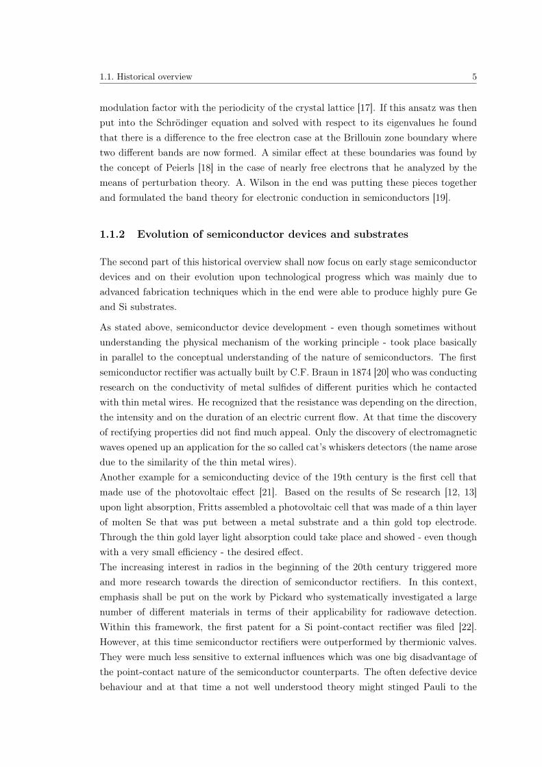
Figure 1.1: An enlarged replica of the first Germanium point-contact transistor (Figure takenfrom Ref. [25]) consisting of a triangle with gold contacts, that is pressed upon the n-typegermanium. Below a copper contact serves as base terminal.
age currents in the OFF-state of the device. However, according to Ref. [29] this wasnot enough to replace the existing Ge technology. Rather two different discoveries wereinitiating the Si age that we are facing today. The first one is connected the passivatingproperty [30] of SiO2 on surface states that are due to dangling bonds of a terminatedSi single crystal. This led to a high quality oxide/semiconductor interface enabling thecontrol of charge carriers through the oxide in Metal-Oxide-Semiconductor (MOS) sys-tems. The next logical step was to extend the existing concept of FETs with this newlyfound feature. With the first implementation of a Si Metal-Oxide-Semiconductor-Field-Effect-Transistor (MOSFET) [31] the triumph of Si slowly began. The second importantdiscovery for Si is provided by the integration capability in the form of integrated cir-cuits which has primarily been investigated by Kilby [32], who recognized that the wireconnection between individual devices was causing major problems. The usage of SiO2
as mask material for different types of lithography was key towards further processingsteps.
1.1.3 Compound semiconductors beyond Silicon
The last part of this section is focussed on building a bridge between developments besideSi technology and current power electronics research. Depending on the type of appli-cation the material properties of Si are limited in terms of e.g. high frequency or hightemperature applications. Further, the yield of optoelectronic devices is enhanced in thecase of a direct band alignment between the conduction band minimum and the valenceband maximum [29]. Therefore, material scientists always kept looking for materials
8 Chapter 1. Introduction to modern power semiconductor devices
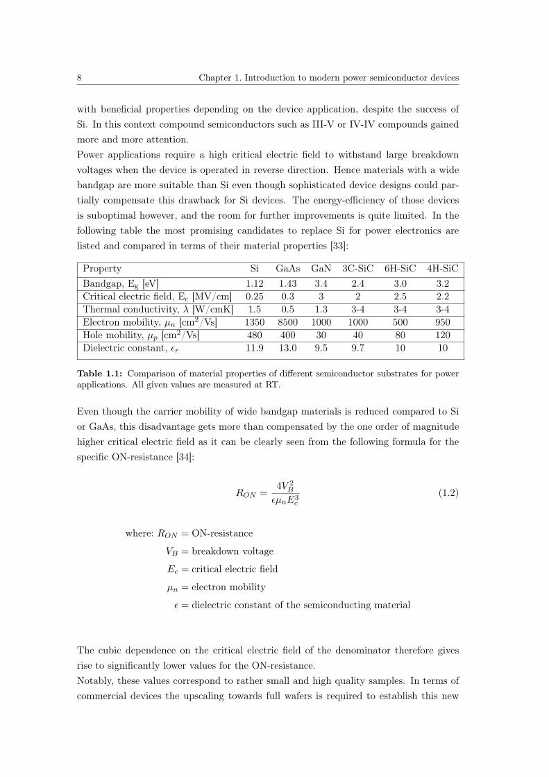
with beneficial properties depending on the device application, despite the success ofSi. In this context compound semiconductors such as III-V or IV-IV compounds gainedmore and more attention.Power applications require a high critical electric field to withstand large breakdownvoltages when the device is operated in reverse direction. Hence materials with a widebandgap are more suitable than Si even though sophisticated device designs could par-tially compensate this drawback for Si devices. The energy-efficiency of those devicesis suboptimal however, and the room for further improvements is quite limited. In thefollowing table the most promising candidates to replace Si for power electronics arelisted and compared in terms of their material properties [33]:
Property Si GaAs GaN 3C-SiC 6H-SiC 4H-SiCBandgap, Eg [eV] 1.12 1.43 3.4 2.4 3.0 3.2Critical electric field, Ec [MV/cm] 0.25 0.3 3 2 2.5 2.2Thermal conductivity, λ [W/cmK] 1.5 0.5 1.3 3-4 3-4 3-4Electron mobility, µn [cm2/Vs] 1350 8500 1000 1000 500 950Hole mobility, µp [cm2/Vs] 480 400 30 40 80 120Dielectric constant, εr 11.9 13.0 9.5 9.7 10 10
Table 1.1: Comparison of material properties of different semiconductor substrates for powerapplications. All given values are measured at RT.
Even though the carrier mobility of wide bandgap materials is reduced compared to Sior GaAs, this disadvantage gets more than compensated by the one order of magnitudehigher critical electric field as it can be clearly seen from the following formula for thespecific ON-resistance [34]:
RON =4V 2
B
εµnE3c
(1.2)
where: RON = ON-resistance
VB = breakdown voltage
Ec = critical electric field
µn = electron mobility
ε = dielectric constant of the semiconducting material
The cubic dependence on the critical electric field of the denominator therefore givesrise to significantly lower values for the ON-resistance.Notably, these values correspond to rather small and high quality samples. In terms ofcommercial devices the upscaling towards full wafers is required to establish this new
1.1. Historical overview 9
technology. A high quality single-crystalline bulk growth of SiC was for a long time amajor obstacle since on the one hand the strength of the Si-C bond was disadvantageousand on the other hand the crystal structure needed to be precisely controlled. The latteris important since SiC crystals can occur with different crystal structures that exhibitdifferent material properties. The so called polytypism is the variation of the crystalstructure depending on the stacking sequence in one direction [35]. For SiC more than200 polytypes are known [36].In contrast to other semiconducting materials, a growth process from a stoichiometricmelt is not possible at technologically relevant temperatures and pressures. Hence single-crystalline bulk SiC was obtained from a sublimation growth technique which goes backto Lely in 1955 [37]. In a graphite crucible SiC powder was heated to approximately2500 C until it sublimes. The mass transport of the sublimed species is governed by atemperature difference between the outer and the inner part of the crucible where singlecrystalline platelets are recrystallized. Even though the overall yield and the control ofthe polytypism were not very high, the material quality of the platelets obtained by thistechnique was high enough to use them as a seed for other growth techniques. Tairovand Tsvetkov developed an advancement based on the seeded sublimation growth [38]which is up to now the most widespread technique.The polytype control of the single crystalline substrate was one of the major issuesin SiC technology since the formation energy for stacking faults is low and thereforepolytype mixing can easily occur [39]. Empirical relations for the stabilization of acertain polytype have been investigated and it was found that the polarity of the seedcrystal as well as the C/Si ratio during growth are key for controlling the polytype of thegrowing substrate. Whether the bulk growth nucleates on a Si or a C face has therbythe highest impact. The former favours the growth of 6H-SiC while the latter results ina 4H-SiC crystal [40].The impurity doping also favours a certain polytype of SiC. This effect mainly dependson the site where the dopant is incorporated in the crystal. Nitrogen atoms e.g. occupy Clattice sites and therefore the growth atmosphere becomes C-rich which facilitates a 4H-SiC growth [41]. The opposite is true for Al which is incorporated as electron acceptor.Therefore the growth of p+ 4H-SiC substrates by sublimation is still challenging.Further, defects due to non-stable growth conditions such as e.g. micropipes compromisethe subsequent homoepitaxial growth of the active device area. However, the ongoingresearch and development effort led to commercially available 6H-SiC in the beginningof the 1990ies. Together with the step flow control technique [42], which makes use ofa certain off-angle to ensure a perfect control over the homoepitaxially grown polytype,the basis for SiC power devices was provided.In retrospect there are similarities between the establishment of a Si-based technologyand the obstacles SiC is facing today even though the processing technology is entirely

10 Chapter 1. Introduction to modern power semiconductor devices
different. One of the biggest problems that SiC technology still encounters are the lowobserved channel mobilities for MOS-controlled devices. In contrast to Si where thepassivation of surface states due to the SiO2 layer was a breakthrough, the complexnature of the oxidation process is still hampering these kind of developments in SiC.Although passivating effects have been achieved by post oxidation annealing treatmentsthe performance of SiC MOSFETs remained limited [43]. Within the fabrication relatedproject of this thesis this problem has been addressed by the anisotropy of the channelmobility with respect to the orientation of the channel to a certain crystallographic axis.

1.2. Power devices and their power electronic applications 11
1.2 Power devices and their power electronic applications
After the historical introduction and an insight into SiC technology within the followingparagraphs and lines the focus shall be given to the application of power electronicdevices. For this purpose a classification either on the current and voltage rating of theapplication or on the power and frequency rating of the underlying devices can be made.
1.2.1 Semiconductor power devices as building blocks for power con-version systems
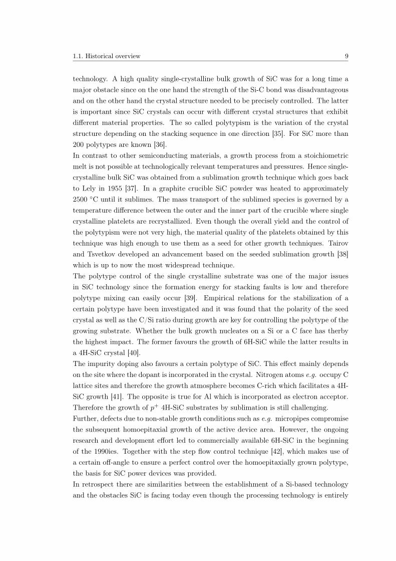
Depending on the type of power conversion, there are four different possible systems. ACpower can be either converted to DC power or to an AC output power with a differentfrequency or voltage. The situation is similar for DC power. Either the voltage of theDC power can be changed or it can be inverted towards an AC output signal.There are various different converter types which realize the desired type of operation[44] but a detailed description would go beyond the scope of this thesis. However, theworking principles of their major device building blocks shall be addressed here.An AC to DC conversion is performed by the rectification property of a two-terminalsemiconductor diode. Depending on the application this can either be done by a p-i-ndiode or by a Schottky diode. The bias polarity of the source determines for both devicesif they either are in their blocking (OFF-state) or in their conducting state (ON-state).Three-terminal devices have an additional control terminal which allows for a fully orsemi-controllable operation. In Fig. 1.2 these power switches are categorized in termsof their power rating and in terms of their operating frequencies.
A brief description of the working principle of each of these devices will be given below[46, 47]:
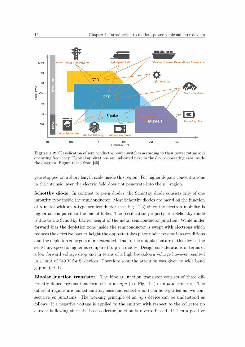
P-i-n diode. The vertical structure of a p-i-n diode (see Fig. 1.3) consists of a narrowand highly doped p+ region followed by the so called intrinsic region which is a lightlyn-doped layer. At the end of this three layer structure is again an n-type layer butthis time with a higher doping concentration. In principle this last layer would not benecessary for the desired rectification properties of the device. The contact formation toa lightly doped n-type layer however is suffering from high contact resistances. There-fore an additional highly doped layer gets introduced at the cathode side of the device.Depending on the dopant concentration of the intrinsic region there are two different de-signs of p-i-n diodes, namely the punch-through and the non-punch-through design. Thisterm is referring to the breakdown electric field in reverse direction which is decreasingaccording to the dopant concentration of the intrinsic layer. If the concentration is lowthe field can penetrate into the n+ layer. Due to the high concentration of this layer it
12 Chapter 1. Introduction to modern power semiconductor devices
Figure 1.2: Classification of semiconductor power switches according to their power rating andoperating frequency. Typical applications are indicated next to the device operating area insidethe diagram. Figure taken from [45]
gets stopped on a short length scale inside this region. For higher dopant concentrationsin the intrinsic layer the electric field does not penetrate into the n+ region.
Schottky diode. In contrast to p-i-n diodes, the Schottky diode consists only of oneimpurity type inside the semiconductor. Most Schottky diodes are based on the junctionof a metal with an n-type semiconductor (see Fig. 1.3) since the electron mobility ishigher as compared to the one of holes. The rectification property of a Schottky diodeis due to the Schottky barrier height of the metal semiconductor junction. While underforward bias the depletion zone inside the semiconductor is swept with electrons whichreduces the effective barrier height the opposite takes place under reverse bias conditionsand the depletion zone gets more extended. Due to the unipolar nature of this device theswitching speed is higher as compared to p-i-n diodes. Design considerations in terms ofa low forward voltage drop and in terms of a high breakdown voltage however resultedin a limit of 240 V for Si devices. Therefore soon the attention was given to wide bandgap materials.
Bipolar junction transistor. The bipolar junction transistor consists of three dif-ferently doped regions that form either an npn (see Fig. 1.4) or a pnp structure. Thedifferent regions are named emitter, base and collector and can be regarded as two con-secutive pn junctions. The working principle of an npn device can be understood asfollows: if a negative voltage is applied to the emitter with respect to the collector nocurrent is flowing since the base collector junction is reverse biased. If then a positive
1.2. Power devices and their power electronic applications 13
Figure 1.3: A schematic illustration of the cross-sections of a p-i-n (left) and a Schottky diode(right) is shown. While the rectifying nature of the p-i-n diode is caused by reverse biasing apn junction, in the Schottky diode the barrier that forms at the metal semiconductor junctiondepends on the bias polarity.
voltage is applied to the base region with respect to the emitter the base emitter junctionis forward biased and electrons get injected into the base and holes will flow towardsthe emitter. Due to recombination processes a lot of these injected carriers will be lostfor the current transport. In the case of a narrow base region however a sufficientlylarge fraction can diffuse towards the base collector junction and will then be attractedby the electric field towards the collector. Hence by controlling the voltage across thebase emitter junction the current flow through the initially reverse biased base collectorjunction can be controlled. If the voltage between the base and the emitter is later onagain switched off the current flow between the emitter and the collector stops since nonew carriers will be injected and the initial state is restored.
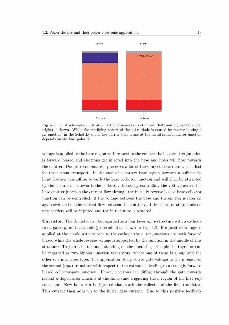
Thyristor. The thyristor can be regarded as a four layer npnp structure with a cathode(n) a gate (p) and an anode (p) terminal as shown in Fig. 1.5. If a positive voltage isapplied at the anode with respect to the cathode the outer junctions are both forwardbiased while the whole reverse voltage is supported by the junction in the middle of thisstructure. To gain a better understanding on the operating principle the thyristor canbe regarded as two bipolar junction transistors, where one of them is a pnp and theother one is an npn type. The application of a positive gate voltage to the p region ofthe second (npn) transistor with respect to the cathode is leading to a strongly forwardbiased collector-gate junction. Hence, electrons can diffuse through the gate towardssecond n-doped area which is at the same time triggering the n region of the first pnptransistor. Now holes can be injected that reach the collector of the first transistor.This current then adds up to the initial gate current. Due to this positive feedback
14 Chapter 1. Introduction to modern power semiconductor devices
Figure 1.4: A schematic illustration of the cross-sections of a bipolar junction transistor isshown. Similar to the npn type depicted here also a pnp device can be realized by inverting thenature of the impurity atoms.
the thyristor remains in its ON-state even though the gate current is switched off. Thedevice can be only switched off if the overall direction of current flow gets reversed. Aspecial case of the thyristor is the Gate Turn off (GTO) thyristor which can be fullyswitched by applying a negative current to the gate.
Figure 1.5: A schematic illustration of the cross-sections of the four layer npnp structure ofa thyristor is shown. For a better understanding of the working principle the thyristor can beregarded as a composition of an npn and an pnp transistor.
MOSFET. As the name already suggests the operating principle of the power MOSFETcritically depends on what is happening at the MOS interface. Depending on the carriertype which is conducting the current the MOSFET is categorized either as n or p-
1.2. Power devices and their power electronic applications 15
channel. In the following, considerations regarding an n-channel MOSFET will be madewhich in a similar manner apply to the p-channel counterpart. In principle, a MOSFETis a four terminal device which consists of a source, a drain, a gate and a body terminal.In the n-channel case the substrate (body terminal) is p-doped with two n-wells at thesurface that form the drain and source terminals (see Fig. 1.6). In order that a channelcan form between drain and source, a gate terminal is needed to control the propertiesof the channel. This terminal is situated above the gate insulator which is SiO2 in thecase of Si or as well for SiC in the case of thermally grown oxides.To understand the operating principle of a lateral MOSFET one has to consider twodistinct electric fields, namely a transverse electric field which is caused by the potentialdifference between the gate and the substrate and a lateral electric field which is due toan applied voltage between the source and the drain region of the device. If a positivevoltage is applied to the gate terminal with respect to the body majority holes will bedepleted from the interface and minority electrons will be accumulated. Depending onthe magnitude of this voltage an inversion layer of electrons can form below the gateoxide. This voltage is known as threshold voltage and enables a current flow betweenthe source and the drain terminals if an appropriate drain-source voltage is applied. Forthe following considerations of the operating regimes the source and body terminals aregrounded.If the gate source voltage does not exceed the threshold voltage no inversion channel isformed and depending on the sign of the drain-source voltage the drain-body diode iseither forward biased for negative VDS resulting in I−V characteristics of a pn junctionor in the forward blocking state for positive VDS where only a small leakage current willflow. In the latter case the depletion region widens into the channel.If the gate source voltage is above the threshold voltage an inversion layer is formedbelow the oxide and electrons can flow from the source to the drain terminal. Dependingon the magnitude of VDS there are different operating regimes. In the linear regime acontinuous channel gets formed. If the drain source voltage is further increased theincreasing space charge region (SCR) of the reverse biased pn junction at the drain sideleads to a constriction of the channel until the channel is not continuous anymore in thesaturation regime.For power applications however, mainly a vertical architecture with the drain contacton the backside of the wafer is used. With this geometry the cell pitch can be reducedas compared to the lateral counterpart which decreases the ON-resistance of the device.A special type of a vertical MOSFET is the Super-Junction (SJ) MOSFET [48] which isbased on the charge compensation of alternating p and n-doped pillars inside the driftregion (see Fig. 1.6). Due to the local charge compensation principle the drift layerexhibits a low effective dopant concentration which supports high voltages in reversedirection. In forward direction this design benefits by the fact that the single pillars

16 Chapter 1. Introduction to modern power semiconductor devices
can exhibit a larger doping concentration as compared to drift layers in pn diodes andtherefore the ON-resistance gets significantly reduced. While in conventional powerMOSFETs the drift layer resistance increases by the desired breakdown voltage accordingto U2.5
BR, this dependence gets diminished towards an almost linear behaviour for the SJ-MOSFET [49].
Figure 1.6: A schematic illustration of the cross-sections of a lateral MOSFET and of a trenchMOSFET consisting of alternating n and p pillars is shown.
IGBT. The structure of an Insulated-Gate-Bipolar-Transistor (IGBT) is very similar tothe one of a vertical double diffused power MOSFET. While in the case of the MOSFETelectrons are injected through the p-well inside the drift layer and later on collected bya highly n-doped drain terminal, the IGBT employs a highly doped p-region at the backof the wafer as shown in Fig. 1.7. The establishment of a channel occurs analogouslyto the case of a MOSFET, only then when a gate voltage that exceeds the thresholdvoltage is applied. Electrons can now flow through the channel into the n-base regionif a positive voltage is applied to the collector with respect to the emitter. At the sametime holes get injected from the p-layer at the collector side which partially recombinewith the injected electrons. The fraction of holes that does not recombine can reach thep-well of the pnp transistor structure.
1.2.2 Applications
As depicted in Fig. 1.2 there is a wide range for power semiconductor applications[41, 44, 50]. For lower power ratings such as for power supplies, power MOSFETs areused as converters since their fast switching speeds are reducing complexity of additionalfiltering components. Automotive electronics that are fed from the onboard power supplyalso make use of MOSFET based power switches.For medium voltage drives that are connected to the grid an effective power conversion

1.2. Power devices and their power electronic applications 17
Figure 1.7: A schematic illustration of the cross-sections of a vertical MOSFET and of anIGBT is shown. The main difference is the dopant type of the layer near the backside contact.
is needed due to the different standards for power grids. The same applies for tractionapplications. Most common devices used for these application types are IGBTs sincemulti-axle designs (where more components are driven by the same converter) are moreand more replaced by single-axle designs. Also the emerging photovoltaic applicationsneed conversion from DC to AC to be fed into the grid which is most effectively doneby IGBTs.The high power spectrum is covered by thyristor based switches. If there is no constantoperating speed of an engine or a turbine as it is the case for wind turbines, the generatedpower needs to be converted before it is fed into the grid. Another application in thehigh power regime is the high voltage DC transmission. Above distances from 800 kmthe higher costs of the DC terminal are redeemed by the lower line costs.


CHAPTER 2
Experimental techniques and processes
Within this chapter the experimental tools regarding the fabrication, preparation andcharacterization will be discussed in detail since the chapters 3, 4 and 5 which arebased on published articles or final stage manuscripts are only refreshing this knowledgeeither by short paragraphs or by citing the appropriate references. The organizationwill thereby follow the structure of this thesis and not the life cycle of a device from itsfabrication to its characterization.
2.1 Cross-section preparation
The requirement of a high blocking voltage capability when the device is operated underreverse bias conditions asks for rather complicated dopant architectures in modern powersemiconductor devices. A plethora of devices therefore employs a vertical geometry thatcontains a thick drift layer to sustain high reverse voltages in addition to the devicespecific dopant distribution. Hence, in a first step, a cross-section of the device underinvestigation needs to prepared to reveal the dopant architecture below the wafer surface.
2.1.1 Chemical-mechanical polishing
The easiest method for the cross-section preparation would be the cleavage of the waferalong one of its crystallographic directions. This can be experimentally realized byscratching the wafer with a diamond scribe. In a second step two tweezers are usedgrab the corresponding halves of the wafer next to the groove. By the application of
19
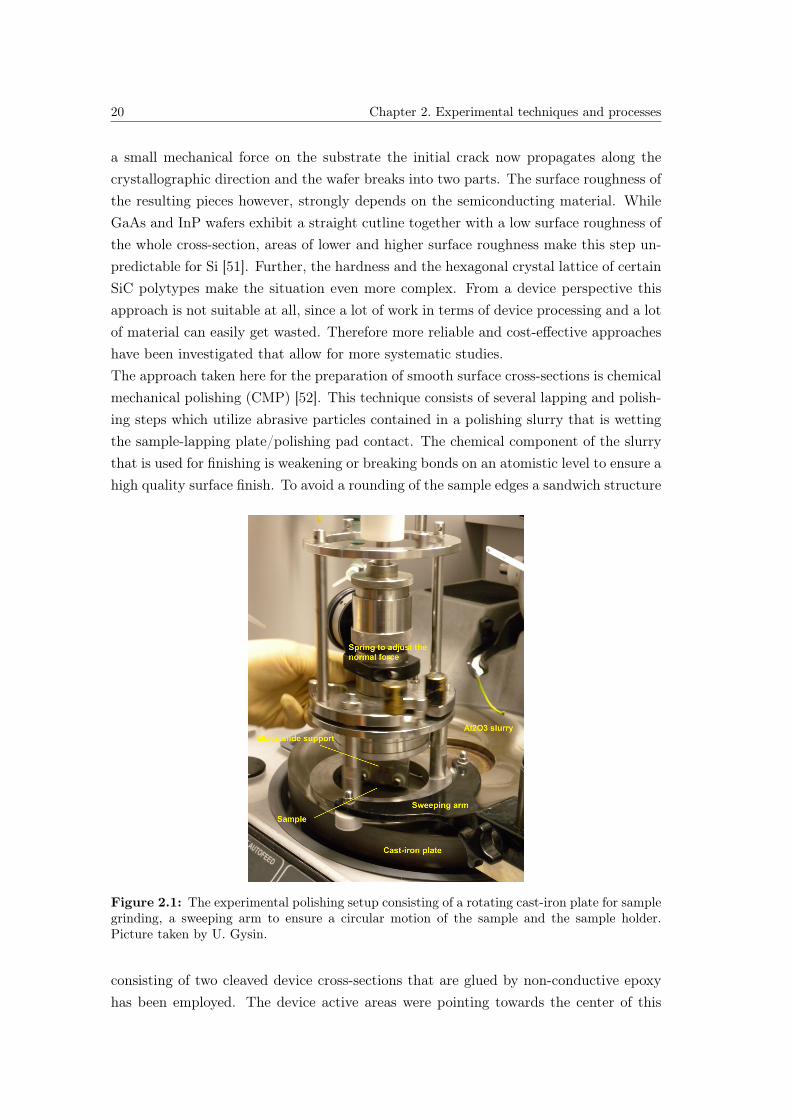
20 Chapter 2. Experimental techniques and processes
a small mechanical force on the substrate the initial crack now propagates along thecrystallographic direction and the wafer breaks into two parts. The surface roughness ofthe resulting pieces however, strongly depends on the semiconducting material. WhileGaAs and InP wafers exhibit a straight cutline together with a low surface roughness ofthe whole cross-section, areas of lower and higher surface roughness make this step un-predictable for Si [51]. Further, the hardness and the hexagonal crystal lattice of certainSiC polytypes make the situation even more complex. From a device perspective thisapproach is not suitable at all, since a lot of work in terms of device processing and a lotof material can easily get wasted. Therefore more reliable and cost-effective approacheshave been investigated that allow for more systematic studies.The approach taken here for the preparation of smooth surface cross-sections is chemicalmechanical polishing (CMP) [52]. This technique consists of several lapping and polish-ing steps which utilize abrasive particles contained in a polishing slurry that is wettingthe sample-lapping plate/polishing pad contact. The chemical component of the slurrythat is used for finishing is weakening or breaking bonds on an atomistic level to ensure ahigh quality surface finish. To avoid a rounding of the sample edges a sandwich structure
Figure 2.1: The experimental polishing setup consisting of a rotating cast-iron plate for samplegrinding, a sweeping arm to ensure a circular motion of the sample and the sample holder.Picture taken by U. Gysin.
consisting of two cleaved device cross-sections that are glued by non-conductive epoxyhas been employed. The device active areas were pointing towards the center of this

2.1. Cross-section preparation 21
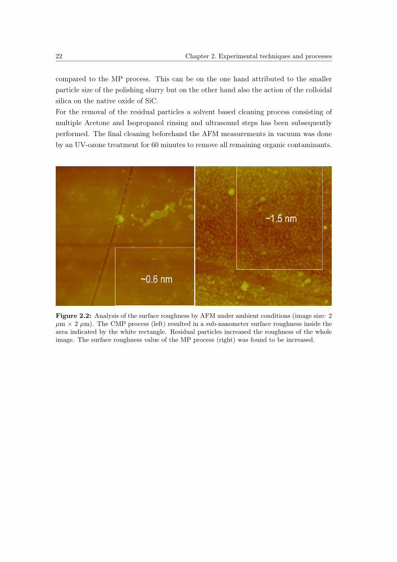
sandwich. As depicted in Fig. 2.1 an additional glass slide supports the sample insidethe chuck. With a spring in the sample holder the normal force can be adjusted. Thesweeping arm of the polishing machine causes a circular motion of the sample for a morehomogeneous process. The parameter space includes the rotating speed of the cast-ironplate/polishing pad, the amount of polishing slurry used and the normal force. Besidethat a fine-tuning with respect to the use of different polishing pads and slurries withvarying particle sizes needs to be done for an optimized polishing result.Due to the different hardness of different semiconducting materials also the polishingprocess can be entirely different. The parameters that can be changed are discussedwithin the next lines on the example of Si and 4H-SiC that are the two semiconductingmaterials used within the scope of this thesis.For the more advanced Si-technology a standard two-step lapping and polishing processhas been developed. Al2O3 particles inside the slurry cater for the mechanical materialremoval of the sample during the grinding step on a rotating cast-iron plate. The sub-sequent polishing step is conducted on a corklike polishing pad in combination with theSyton SF1 polishing suspension that consists of colloidal silica particles with an averagediameter of 250 nm. In a first step the chemical component induces a reaction of surfacemolecules into soluble complexes that can later on be mechanically removed [53].SiC is a more challenging semiconducting material in terms of polishing due to its hard-ness of 9.6 on the Mohs scale which is very close to diamond. Hence, only diamondparticles can be used as abrasive materials. In the following table the polishing pa-rameters for a mechanical (MP) and a chemical-mechanical process (CMP) for 4H-SiCare shown: According to Fig. 2.2 the surface roughness for the CMP process is lower
CMPStep Disk Grain size [µm] Rot. [rpm] Weight [g] Time [min]Grinding Cast-iron disk 6 50 300 3Polishing Microtex 3 30 400 60Polishing Microtex 1 15 400 30Polishing Chemcloth 0.25 15 400 15
MPStep Disk Grain size [µm] Rot. [rpm] Weight [g] Time [min]Grinding Cast-iron disk 6 50 300 3Polishing Microtex 3 30 400 60Polishing Microtex 1 15 400 30Polishing MD-Nap 1 15 400 30
Table 2.1: Comparison of a chemical-mechanical and a mechanical polishing process for 4H-SiCin terms of their process parameters. While the first three steps are equal the finishing step forthe CMP process is identical to processes used for Si and the MP process is based on a smallgrain size diamond slurry in combination with a very soft polishing pad.
22 Chapter 2. Experimental techniques and processes
compared to the MP process. This can be on the one hand attributed to the smallerparticle size of the polishing slurry but on the other hand also the action of the colloidalsilica on the native oxide of SiC.For the removal of the residual particles a solvent based cleaning process consisting ofmultiple Acetone and Isopropanol rinsing and ultrasound steps has been subsequentlyperformed. The final cleaning beforehand the AFM measurements in vacuum was doneby an UV-ozone treatment for 60 minutes to remove all remaining organic contaminants.
Figure 2.2: Analysis of the surface roughness by AFM under ambient conditions (image size: 2µm × 2 µm). The CMP process (left) resulted in a sub-nanometer surface roughness inside thearea indicated by the white rectangle. Residual particles increased the roughness of the wholeimage. The surface roughness value of the MP process (right) was found to be increased.
2.2. SPM-based characterization methods 23
2.2 SPM-based characterization methods
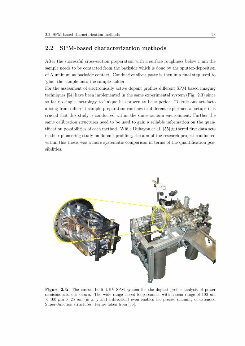
After the successful cross-section preparation with a surface roughness below 1 nm thesample needs to be contacted from the backside which is done by the sputter-depositionof Aluminum as backside contact. Conductive silver paste is then in a final step used to‘glue’ the sample onto the sample holder.For the assessment of electronically active dopant profiles different SPM based imagingtechniques [54] have been implemented in the same experimental system (Fig. 2.3) sinceso far no single metrology technique has proven to be superior. To rule out artefactsarising from different sample preparation routines or different experimental setups it iscrucial that this study is conducted within the same vacuum environment. Further thesame calibration structures need to be used to gain a reliable information on the quan-tification possibilities of each method. While Duhayon et al. [55] gathered first data setsin their pioneering study on dopant profiling, the aim of the research project conductedwithin this thesis was a more systematic comparison in terms of the quantification pos-sibilities.
Figure 2.3: The custom-built UHV-SPM system for the dopant profile analysis of powersemiconductors is shown. The wide range closed loop scanner with a scan range of 100 µm× 100 µm × 25 µm (in x, y and z-direction) even enables the precise scanning of extendedSuper-Junction structures. Figure taken from [56].
24 Chapter 2. Experimental techniques and processes
2.2.1 Kelvin Probe Force Microscopy
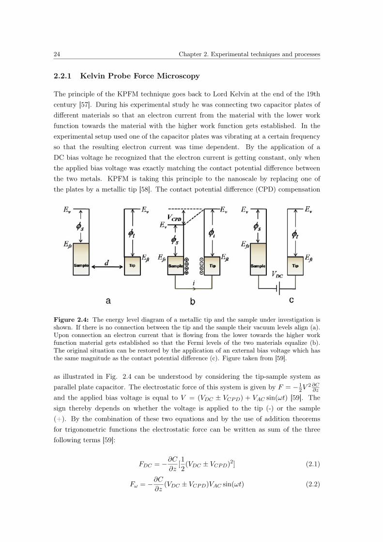
The principle of the KPFM technique goes back to Lord Kelvin at the end of the 19thcentury [57]. During his experimental study he was connecting two capacitor plates ofdifferent materials so that an electron current from the material with the lower workfunction towards the material with the higher work function gets established. In theexperimental setup used one of the capacitor plates was vibrating at a certain frequencyso that the resulting electron current was time dependent. By the application of aDC bias voltage he recognized that the electron current is getting constant, only whenthe applied bias voltage was exactly matching the contact potential difference betweenthe two metals. KPFM is taking this principle to the nanoscale by replacing one ofthe plates by a metallic tip [58]. The contact potential difference (CPD) compensation
Figure 2.4: The energy level diagram of a metallic tip and the sample under investigation isshown. If there is no connection between the tip and the sample their vacuum levels align (a).Upon connection an electron current that is flowing from the lower towards the higher workfunction material gets established so that the Fermi levels of the two materials equalize (b).The original situation can be restored by the application of an external bias voltage which hasthe same magnitude as the contact potential difference (c). Figure taken from [59].
as illustrated in Fig. 2.4 can be understood by considering the tip-sample system asparallel plate capacitor. The electrostatic force of this system is given by F = −1
2V2 ∂C∂z
and the applied bias voltage is equal to V = (VDC ± VCPD) + VAC sin(ωt) [59]. Thesign thereby depends on whether the voltage is applied to the tip (-) or the sample(+). By the combination of these two equations and by the use of addition theoremsfor trigonometric functions the electrostatic force can be written as sum of the threefollowing terms [59]:
FDC = −∂C∂z
[1
2(VDC ± VCPD)2] (2.1)
Fω = −∂C∂z
(VDC ± VCPD)VAC sin(ωt) (2.2)
2.2. SPM-based characterization methods 25
F2ω =∂C
∂z
1
4V 2AC [cos(2ωt)− 1] (2.3)
While the first term either gets nullified by the compensation of the contact potentialdifference, which is defined as VCPD =
Φsample−Φtip
q , or results in a static deflection of thecantilever, KPFM utilizes the Fω component to measure the contact potential differenceof the tip-sample system. The F2ω term can be used for capacitance measurementsas will be discussed in the following subsection. The working principle of KPFM is
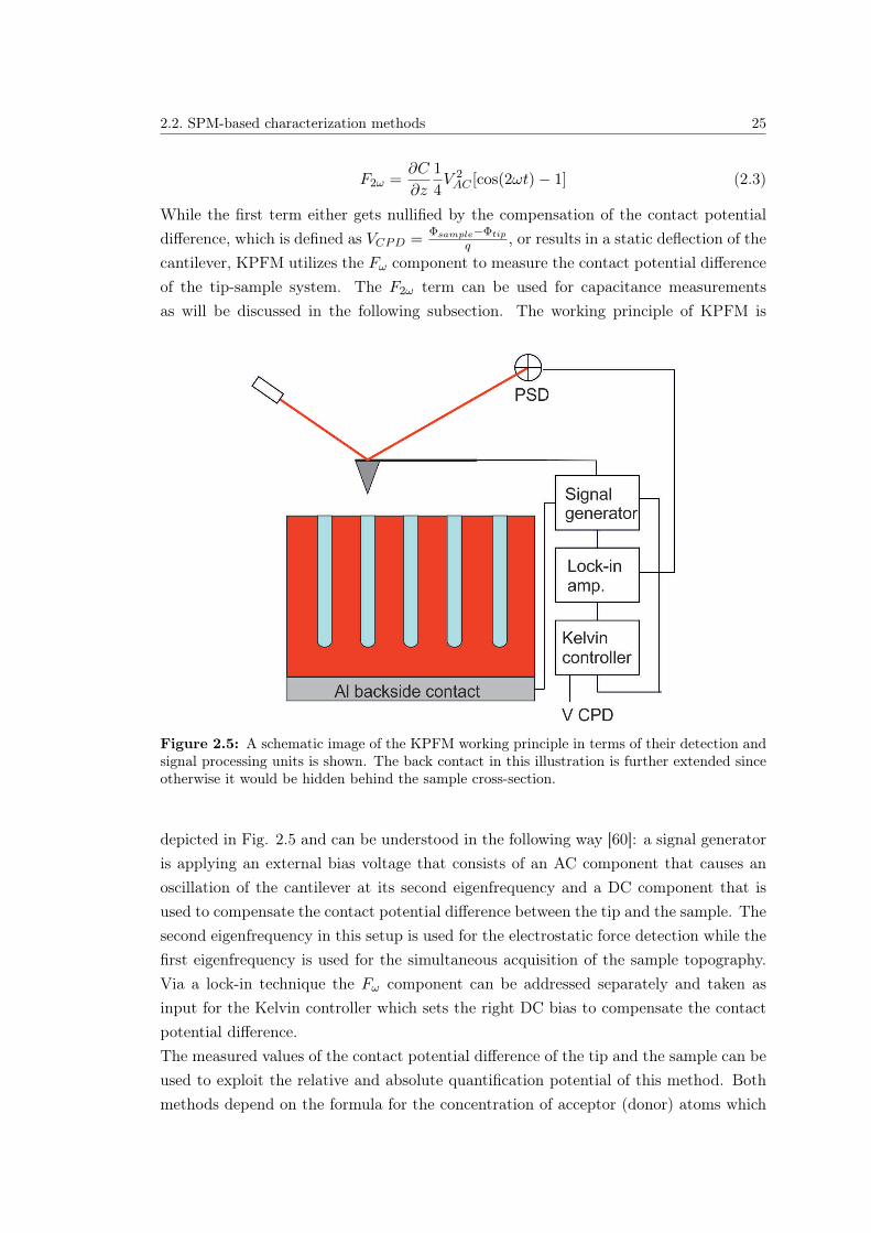
Figure 2.5: A schematic image of the KPFM working principle in terms of their detection andsignal processing units is shown. The back contact in this illustration is further extended sinceotherwise it would be hidden behind the sample cross-section.
depicted in Fig. 2.5 and can be understood in the following way [60]: a signal generatoris applying an external bias voltage that consists of an AC component that causes anoscillation of the cantilever at its second eigenfrequency and a DC component that isused to compensate the contact potential difference between the tip and the sample. Thesecond eigenfrequency in this setup is used for the electrostatic force detection while thefirst eigenfrequency is used for the simultaneous acquisition of the sample topography.Via a lock-in technique the Fω component can be addressed separately and taken asinput for the Kelvin controller which sets the right DC bias to compensate the contactpotential difference.The measured values of the contact potential difference of the tip and the sample can beused to exploit the relative and absolute quantification potential of this method. Bothmethods depend on the formula for the concentration of acceptor (donor) atoms which
26 Chapter 2. Experimental techniques and processes
is given by
NA = NV exp
(−EsampleF − EV
kBT
)(2.4)
whereNA is the acceptor concentration, NV is the density of valence band states, EsampleF
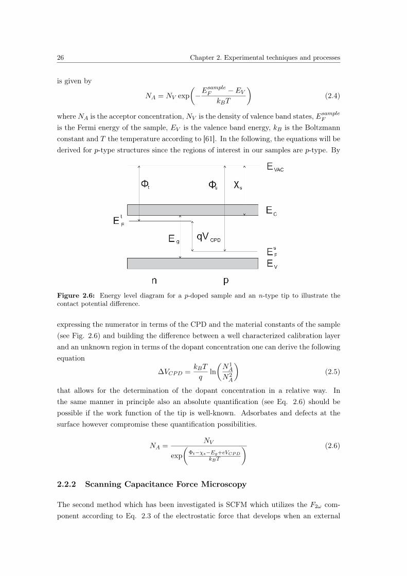
is the Fermi energy of the sample, EV is the valence band energy, kB is the Boltzmannconstant and T the temperature according to [61]. In the following, the equations will bederived for p-type structures since the regions of interest in our samples are p-type. By
Figure 2.6: Energy level diagram for a p-doped sample and an n-type tip to illustrate thecontact potential difference.
expressing the numerator in terms of the CPD and the material constants of the sample(see Fig. 2.6) and building the difference between a well characterized calibration layerand an unknown region in terms of the dopant concentration one can derive the followingequation
∆VCPD =kBT
qln
(N1A
N2A
)(2.5)
that allows for the determination of the dopant concentration in a relative way. Inthe same manner in principle also an absolute quantification (see Eq. 2.6) should bepossible if the work function of the tip is well-known. Adsorbates and defects at thesurface however compromise these quantification possibilities.
NA =NV
exp
(Φt−χs−Eg+eVCPD
kBT
) (2.6)
2.2.2 Scanning Capacitance Force Microscopy
The second method which has been investigated is SCFM which utilizes the F2ω com-ponent according to Eq. 2.3 of the electrostatic force that develops when an external
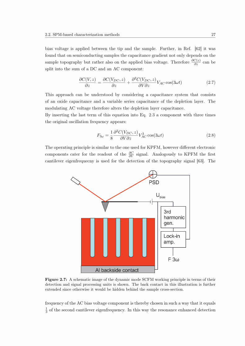
2.2. SPM-based characterization methods 27
bias voltage is applied between the tip and the sample. Further, in Ref. [62] it wasfound that on semiconducting samples the capacitance gradient not only depends on thesample topography but rather also on the applied bias voltage. Therefore ∂C(z)
∂z can besplit into the sum of a DC and an AC component:
∂C(V, z)
∂z=∂C(VDC , z)
∂z+∂2C(VDC , z)
∂V ∂zVAC cos(3ωt) (2.7)
This approach can be understood by considering a capacitance system that consistsof an oxide capacitance and a variable series capacitance of the depletion layer. Themodulating AC voltage therefore alters the depletion layer capacitance.By inserting the last term of this equation into Eq. 2.3 a component with three timesthe original oscillation frequency appears:
F3ω =1
8
∂2C(VDC , z)
∂V ∂zV 3AC cos(3ωt) (2.8)
The operating principle is similar to the one used for KPFM, however different electroniccomponents cater for the readout of the ∂C
∂V signal. Analogously to KPFM the firstcantilever eigenfrequecny is used for the detection of the topography signal [63]. The
Figure 2.7: A schematic image of the dynamic mode SCFM working principle in terms of theirdetection and signal processing units is shown. The back contact in this illustration is furtherextended since otherwise it would be hidden behind the sample cross-section.
frequency of the AC bias voltage component is thereby chosen in such a way that it equals13 of the second cantilever eigenfrequency. In this way the resonance enhanced detection
28 Chapter 2. Experimental techniques and processes
principle can be exploited. A frequency converter is generating the third harmonic ofthis AC bias as input signal of the lock-in amplifier so that the right component ofthe electrostatic force signal can be selected for mapping the F3ω signal. Notably, thedepletion width is larger the smaller the doping concentration is. Hence, the change ofthe total capacitance is larger in the low dopant concentration regime. Bias spectroscopymeasurements have confirmed this trend, however the shape of these curves is not yetwell understood so that dopant profiling in a quantitative manner is still not possible.Technology Computer Aided Design (TCAD) simulations on this issue are ongoing [64]so that the potential of this method can be addressed in future work.
2.2.3 Scanning Spreading Resistance Microscopy
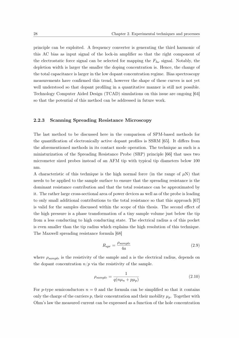
The last method to be discussed here in the comparison of SPM-based methods forthe quantification of electronically active dopant profiles is SSRM [65]. It differs fromthe aforementioned methods in its contact mode operation. The technique as such is aminiaturization of the Spreading Resistance Probe (SRP) principle [66] that uses twomicrometer sized probes instead of an AFM tip with typical tip diameters below 100nm.A characteristic of this technique is the high normal force (in the range of µN) thatneeds to be applied to the sample surface to ensure that the spreading resistance is thedominant resistance contribution and that the total resistance can be approximated byit. The rather large cross-sectional area of power devices as well as of the probe is leadingto only small additional contributions to the total resistance so that this approach [67]is valid for the samples discussed within the scope of this thesis. The second effect ofthe high pressure is a phase transformation of a tiny sample volume just below the tipfrom a less conducting to high conducting state. The electrical radius a of this pocketis even smaller than the tip radius which explains the high resolution of this technique.The Maxwell spreading resistance formula [68]
Rspr =ρsample
4a(2.9)
where ρsample is the resistivity of the sample and a is the electrical radius, depends onthe dopant concentration n/p via the resistivity of the sample.
ρsample =1
q(nµn + pµp)(2.10)
For p-type semiconductors n = 0 and the formula can be simplified so that it containsonly the charge of the carriers p, their concentration and their mobility µp. Together withOhm’s law the measured current can be expressed as a function of the hole concentration
2.2. SPM-based characterization methods 29
is given byI = 4aeUpµp (2.11)
whereas U is a DC bias voltage that is applied between the tip and the sample back-contact. The topography is monitored by a beam deflection setup while the dopant
Figure 2.8: A schematic image of the SSRM working principle in terms of their detection andsignal processing units is shown. The back contact in this illustration is further extended sinceotherwise it would be hidden behind the sample cross-section.
dependent current is the output signal of a logarithmic amplifier. Even tough thisprinciple seems to be quite straightforward numerous deviations from this ideal situationmake the quantification more complex. For instance, the carrier mobility depends onthe dopant concentration itself and on the sample temperature. While the latter hasnot a big influence, the change of the carrier mobility for intermediate concentrationsin the order NA = 1017 cm-3 is quite significant [34]. Further, the nature of the nano-contact between the tip and the sample is not ohmic but shows Schottky-like featuresin spectroscopic measurements. All of these examples are topics of current research andwill be discussed later on in Chapter 3.Due to this non-idealities a calibration procedure was up to now based on the use of well-characterized staircase samples [69] with a varying dopant concentration. By comparingthe resistivity profiles of this reference conclusions on the dopant concentration of anunknown sample can be drawn. The strength of this method - as demonstrated byEyben et al. [70] - lies in the high degree of reproducibility. The abrasive action of thetip while scanning the sample in contact mode leads to a self-preparation of the surface.Therefore SSRM is less sensitive to preparation induced defects as the two non-contactmethods discussed before.
30 Chapter 2. Experimental techniques and processes
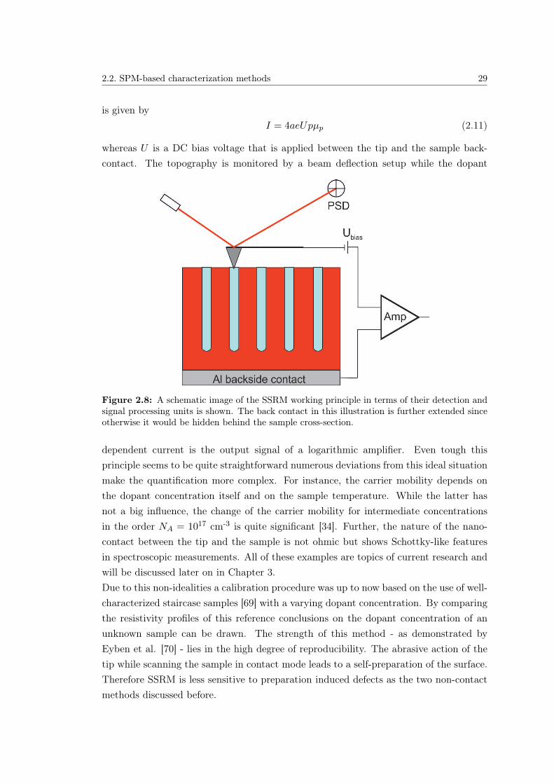
2.3 Trench MOSFET fabrication and mobility measurements
The second part of this methodological introduction is dedicated to the fabrication ofnanoscale trench MOSFETs in 4H-SiC. Therefore a dry etching process with the aimof fabricating trenches of 3 µm in depth and widths ranging from 0.5 µm to 3 µm hadbeen developed. The establishment of a highly controllable and reliable etching processis crucial for further device processing and a successful integration of nano and micro-trenches can be used as platform for different device architectures such as MOSFETs orMOS-Capacitors. In Fig. 2.9a-d the main fabrication steps towards a trench MOSFET
Figure 2.9: The main fabrication steps towards a working MOSFET are shown. The dopantimplantation and activation (a) is followed by a trench etching process (b). Afterwards theU-shaped trench can be oxidized and filled with a doped polycrystalline Si gate. In a last stepmetal contacts that show an ohmic behaviour need to be deposited (d). Figure adapted from[71].
are shown. Main focus in this section will be given to the dry etching process sinceit had been developed at LMN. Further, the main processing steps and the remainingchallenges of the full fabrication process flow will be briefly discussed to gain a betterinsight on the device manufacturing. In the last subsection of this chapter the electricalcharacterization technique for mapping the mobility inside the thin conducting channelwill be discussed.

2.3. Trench MOSFET fabrication and mobility measurements 31
2.3.1 Ion implantation
The first step in the process flow towards a working trench MOSFET is the realizationof the targeted dopant architecture. The impurity type of the source and drain regionsas well as of the substrate determine the type of the transistor. Within this project ann-channel transistor had been designed. Therefore, donor impurities need to be incor-porated into the p-doped substrate. As shown in Fig. 2.9a the method of choice for SiCis ion implantation since the dopant atoms suffer from very low diffusion coefficients.This is on the hand beneficial for the design of shallow junctions but on the other handa selective dopant process by diffusion is not feasible. In Si technology however, ion im-plantation also almost completely replaced thermal diffusion processes due to the betterlateral confinement of impurity atoms [52].Due to the missing availability of an ion implantation source at PSI the implantationprocess had been outsourced to a subcontractor who performed the dopant profile sim-ulations and also the did implantation of Phosphorous atoms to form n+ wells in thep-doped substrate. Further, also n-type substrates with highly Aluminum doped sourceand drain regions have been investigated.For the implantation process itself dopant atoms that are primarily in a gaseous stateneed to be ionized and extracted from the ion source so that they can be later on fil-tered according to their mass. After passing through an acceleration tube the ion beamis spread over the whole wafer by an appropriate electromagnetic lens system. Insidethe wafer the ions are stopped by numerous, stochastic nuclear and electron stoppingprocesses [72]. Therefore simulations on the implantation process are required to predictthe right processing parameters. Within this project the ion energy needed to be chosenin such a way that a 200 nm deep box profile is accomplished. As shown in Fig. 2.10 thetargeted depth profile of the implantation could be reached by an implantation energyof 20 keV. Notably, for SiC the implantation process has to be performed at elevatedtemperatures to avoid an amorphization of the substrate [41]. Hence, a temperature of500 C had been chosen to limit the damage to the crystal lattice. During the subsequenthigh temperature dopant activation step the remaining irregularities of the crystal latticealmost completely vanish so that the crystalline nature gets restored without changingthe polytype during this processing sequence.
2.3.2 Inductively coupled plasma reactive ion etching of trenches
The patterning of the trench structures was done by electron beam lithography [52].In a first step a 100 nm thick Cr hard mask was deposited on top of the wafer. Afterspincoating a Polymethylmethacrylat (PMMA) layer on top, an electron beam was usedto break the bonds of the resist at the positions where the trenches later on shouldbe etched. The selective opening of the hard mask was then obtained by a Cl2 based
32 Chapter 2. Experimental techniques and processes
Figure 2.10: Simulated dopant profiles provided by Ion Beam Services are shown for phospho-rous and aluminum as n and p-type dopant atoms respectively. A box profile with a depth of200 nm had been realized with an implantation energy of 20 keV and an implantation angle of0 degrees. Simulations performed by Ion Beam Services.
reactive ion etching (RIE) process. Chromium had been chosen as hard mask materialsince photoresist or silicon dioxide are not suitable for etching deep trenches into 4H-SiCdue to their limited selectivity. The shape after the etching process was monitored byour in-house SEM.The etching mechanism of RIE systems consists of two components, namely a physicaland a chemical component [52]. The first leads to a mechanical removal of the targetmaterial by the impinging ions as for example in an ion milling process. The chemicalcomponent comes into play by the gases that are used to create the plasma. They arechosen in such a way that they can react with the surface atoms or molecules of thesubstrate to form a more volatile species that can be easily removed.Within the experimental work of this thesis an Oxford plasma lab RIE system that isequipped with an inductively coupled plasma (ICP) head had been used. The plasmathereby gets generated by a radio-frequency (RF) source which creates a time varyingmagnetic field. As a consequence an electric field gets induced inside the plasma chamber.Due to the different masses of the electrons and ions contained inside the plasma, thefast response of the electrons to the varying electric field causes further ionizations ofgas molecules [73]. The forward power creates a DC bias between the charge neutralplasma and the electrode where the sample is mounted, so that vertical ion flux towardsthe sample gets established. With the geometry as shown in Fig. 2.11 the plasma
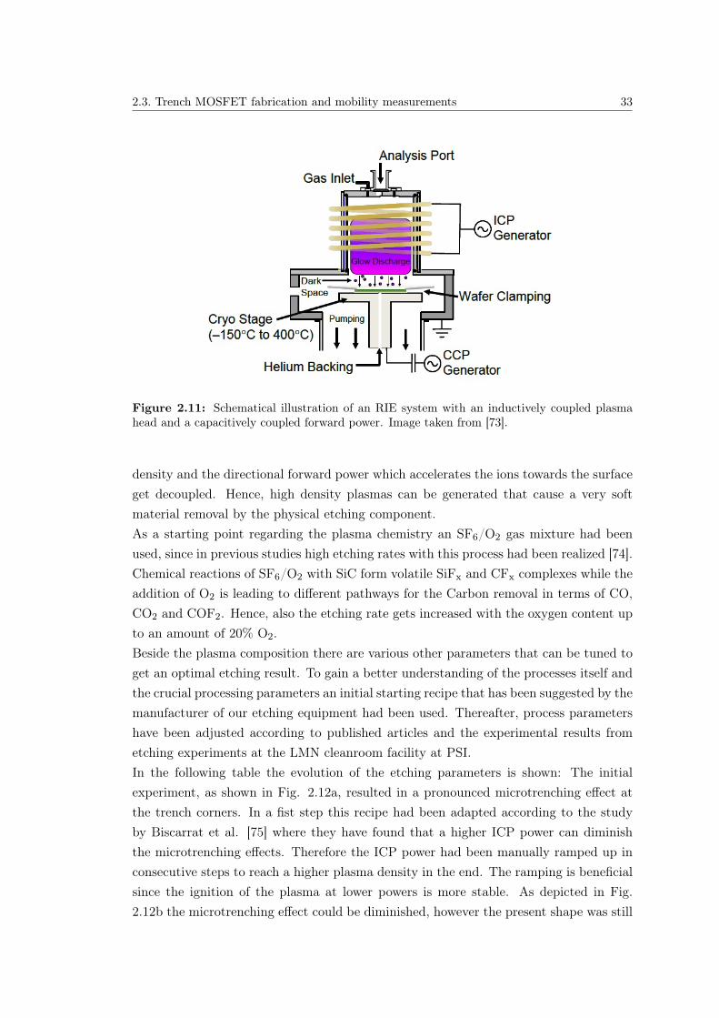
2.3. Trench MOSFET fabrication and mobility measurements 33
Figure 2.11: Schematical illustration of an RIE system with an inductively coupled plasmahead and a capacitively coupled forward power. Image taken from [73].
density and the directional forward power which accelerates the ions towards the surfaceget decoupled. Hence, high density plasmas can be generated that cause a very softmaterial removal by the physical etching component.As a starting point regarding the plasma chemistry an SF6/O2 gas mixture had beenused, since in previous studies high etching rates with this process had been realized [74].Chemical reactions of SF6/O2 with SiC form volatile SiFx and CFx complexes while theaddition of O2 is leading to different pathways for the Carbon removal in terms of CO,CO2 and COF2. Hence, also the etching rate gets increased with the oxygen content upto an amount of 20% O2.Beside the plasma composition there are various other parameters that can be tuned toget an optimal etching result. To gain a better understanding of the processes itself andthe crucial processing parameters an initial starting recipe that has been suggested by themanufacturer of our etching equipment had been used. Thereafter, process parametershave been adjusted according to published articles and the experimental results frometching experiments at the LMN cleanroom facility at PSI.In the following table the evolution of the etching parameters is shown: The initialexperiment, as shown in Fig. 2.12a, resulted in a pronounced microtrenching effect atthe trench corners. In a fist step this recipe had been adapted according to the studyby Biscarrat et al. [75] where they have found that a higher ICP power can diminishthe microtrenching effects. Therefore the ICP power had been manually ramped up inconsecutive steps to reach a higher plasma density in the end. The ramping is beneficialsince the ignition of the plasma at lower powers is more stable. As depicted in Fig.2.12b the microtrenching effect could be diminished, however the present shape was still

34 Chapter 2. Experimental techniques and processes
Process I II III IVSF6 flow [sccm] 10 10 10 10O2 flow [sccm] 2 2 0 0Ar flow [sccm] 0 0 0 2Pressure [mTorr] 10 10 8 10RF power [W] 30 30 7 11ICP power [W] 500 1000 1000 1000VDC [V] 115 70 11 10Time [min] 20 15 20 20Etching rate [nm/min] 155 165 80 65
Table 2.2: Comparison of etching parameters for different processes. Process I refers to theinitial starting recipe from Oxford instruments. Processes II, III and IV have been improvedaccording to published articles and the acquired experimental results.
not satisfactory since these edges would cause a crowding of the electric field during thedevice operation and would therefore lead to a premature breakdown of the device.An other suggestion, namely to reduce the DC bias voltage to a value around 10 V,came from our industrial collaborator ABB. At the same time also the plasma chemistrywas changed since it has been found for 6H-SiC [76] that the O2 fraction can cause theformation of a SiFxOy that is more easily charged than the SiC substrate. Hence moreions will be deflected towards the trench corners. Even tough the pressure for processIII was slightly lower than for process IV (see table 2.2) the obtained trench profile2.13a showed a higher degree of isotropy. Therefore it can be concluded that the effectof the pressure did not lead to the superior trench shape in Fig. 2.13b. Whether themicrotrenching could be eliminated by the smaller DC bias or by the omission of O2 isstill under investigation. Also a combination of both effects is plausible.
2.3.3 Oxidation process
One of the unique properties of SiC - that has also driven the material development interms of power semiconductor applications - is that a SiO2 layer can be thermally grown.As mentioned in Chapter 1 the passivating nature of SiO2 on dangling bonds of the Sicrystal was one major breakthroughs in Si technology. In SiC however, the presence of Catoms makes the situation more complex and the origin of the reduced carrier mobilityat the SiO2/SiC interface is not yet fully understood.To take the presence of C atoms during the thermal oxidation process into account theDeal Grove model for Si [77]
dox +Ad2ox = Bt (2.12)
where dox is the oxide thickness, t is the oxidation time and B and BA are the parabolic
and linear rate constants, has been extended by considering the out-diffusion of product
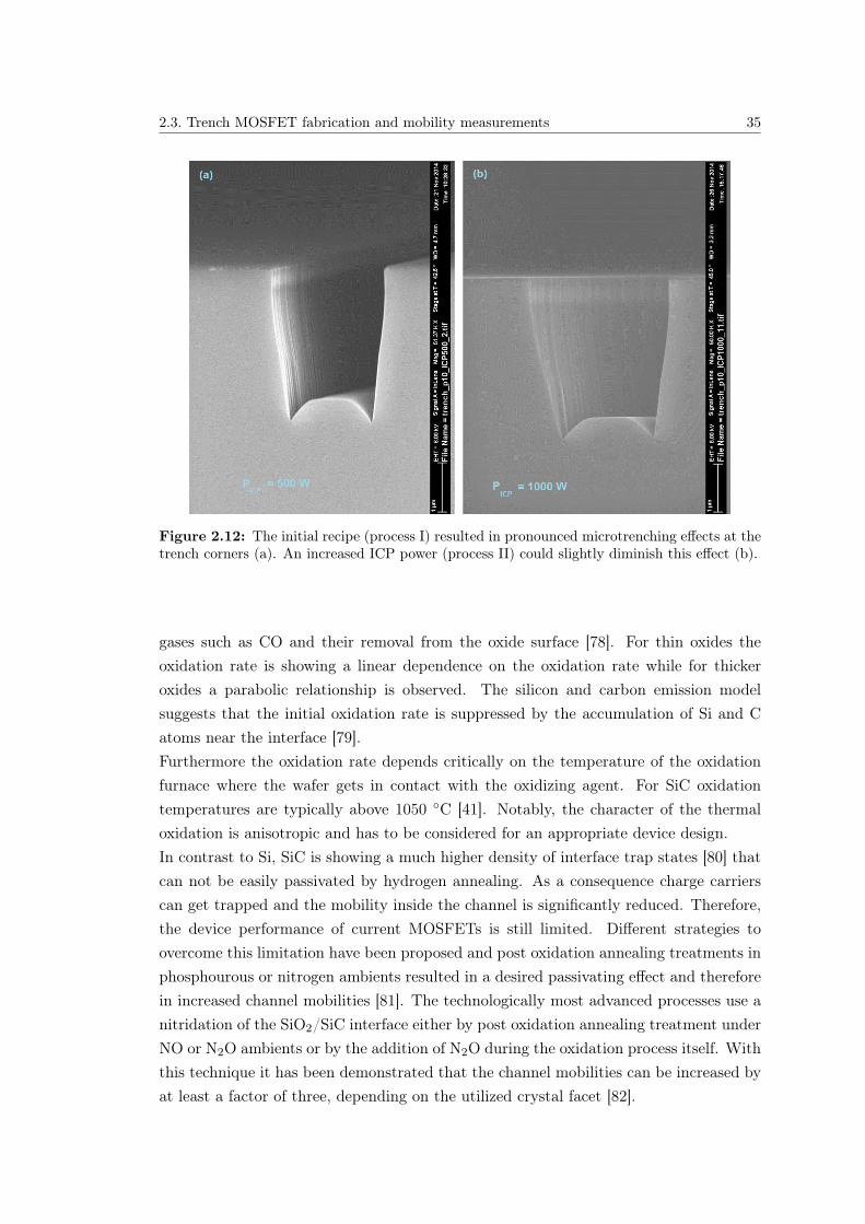
2.3. Trench MOSFET fabrication and mobility measurements 35
Figure 2.12: The initial recipe (process I) resulted in pronounced microtrenching effects at thetrench corners (a). An increased ICP power (process II) could slightly diminish this effect (b).
gases such as CO and their removal from the oxide surface [78]. For thin oxides theoxidation rate is showing a linear dependence on the oxidation rate while for thickeroxides a parabolic relationship is observed. The silicon and carbon emission modelsuggests that the initial oxidation rate is suppressed by the accumulation of Si and Catoms near the interface [79].Furthermore the oxidation rate depends critically on the temperature of the oxidationfurnace where the wafer gets in contact with the oxidizing agent. For SiC oxidationtemperatures are typically above 1050 C [41]. Notably, the character of the thermaloxidation is anisotropic and has to be considered for an appropriate device design.In contrast to Si, SiC is showing a much higher density of interface trap states [80] thatcan not be easily passivated by hydrogen annealing. As a consequence charge carrierscan get trapped and the mobility inside the channel is significantly reduced. Therefore,the device performance of current MOSFETs is still limited. Different strategies toovercome this limitation have been proposed and post oxidation annealing treatments inphosphourous or nitrogen ambients resulted in a desired passivating effect and thereforein increased channel mobilities [81]. The technologically most advanced processes use anitridation of the SiO2/SiC interface either by post oxidation annealing treatment underNO or N2O ambients or by the addition of N2O during the oxidation process itself. Withthis technique it has been demonstrated that the channel mobilities can be increased byat least a factor of three, depending on the utilized crystal facet [82].
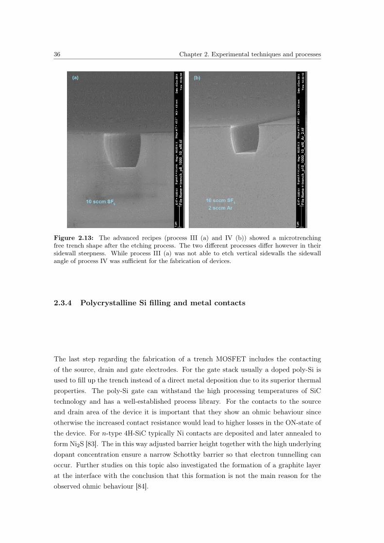
36 Chapter 2. Experimental techniques and processes
Figure 2.13: The advanced recipes (process III (a) and IV (b)) showed a microtrenchingfree trench shape after the etching process. The two different processes differ however in theirsidewall steepness. While process III (a) was not able to etch vertical sidewalls the sidewallangle of process IV was sufficient for the fabrication of devices.
2.3.4 Polycrystalline Si filling and metal contacts
The last step regarding the fabrication of a trench MOSFET includes the contactingof the source, drain and gate electrodes. For the gate stack usually a doped poly-Si isused to fill up the trench instead of a direct metal deposition due to its superior thermalproperties. The poly-Si gate can withstand the high processing temperatures of SiCtechnology and has a well-established process library. For the contacts to the sourceand drain area of the device it is important that they show an ohmic behaviour sinceotherwise the increased contact resistance would lead to higher losses in the ON-state ofthe device. For n-type 4H-SiC typically Ni contacts are deposited and later annealed toform Ni2S [83]. The in this way adjusted barrier height together with the high underlyingdopant concentration ensure a narrow Schottky barrier so that electron tunnelling canoccur. Further studies on this topic also investigated the formation of a graphite layerat the interface with the conclusion that this formation is not the main reason for theobserved ohmic behaviour [84].

2.3. Trench MOSFET fabrication and mobility measurements 37
2.3.5 Assessment of channel mobilities
The effective mobility of an n-channel MOS-controlled FET is given by
µeff =gdL
WQn(2.13)
where L is the channel length, W is the channel width, Qn is the mobile channel chargedensity and gd is the drain conductance which is defined as the change of the draincurrent with respect to the drain-source voltage when the gate-source voltage is keptconstant [85]:
gd =∂ID∂VDS
(2.14)
The mobile channel charge density needs to be determined in the following way: in afirst step the capacitance of the source and drain region is measured in the accumulationregime. Since under these conditions no channel is formed, only the two overlap capaci-tances of the drain and source regions are measured when the substrate is grounded. Ina second step, at a sufficiently high gate voltage, an inversion layer is formed and there-fore also the channel capacitance contributes to the overall capacitance signal. From thedifference of these two capacitance values conclusions on the mobile channel charge canbe drawn. The drain conductance can be extracted from the slope of the drain outputcharacteristics. Together with the geometrical parameters of the channel, the effectivechannel mobility can be evaluated using Eq. 2.13.

CHAPTER 3
Low dopant regime carrier profiling by SPM methods
Within this chapter the answer to the question if there is any SPM based method thatcan quantitatively map carrier concentrations with a high sensitivity shall be given.For the evaluation, the three most promising techniques, namely Kelvin Probe ForceMicroscopy (KPFM), Scanning Capacitance Force Microscopy (SCFM) and ScanningSpreading Resistance Microscopy (SSRM) have been implemented in the same, custom-built vacuum system. To gain meaningful results special test structures with a very lowdopant concentration have been manufactured and assessed with the aforementionedmethods. Even though some of them may look on the first sight quite similar, theunderlying physical contrast mechanism is different and leads to significant differencesin terms of their resolution. After discussing strengths and weaknesses of each method,in the second part of this chapter a detailed analysis of the quantification potential ofmost superior technique SSRM, will be given. It will be shown that there are severalways to determine the carrier concentration profile. Among them, different principleseither based on the depletion width or on the underlying carrier mobility are discussed.
39
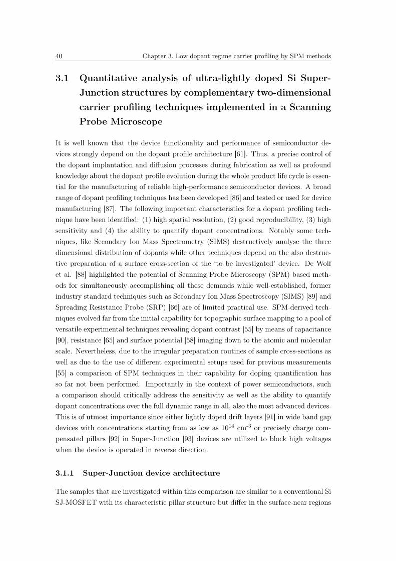
40 Chapter 3. Low dopant regime carrier profiling by SPM methods
3.1 Quantitative analysis of ultra-lightly doped Si Super-Junction structures by complementary two-dimensionalcarrier profiling techniques implemented in a ScanningProbe Microscope
It is well known that the device functionality and performance of semiconductor de-vices strongly depend on the dopant profile architecture [61]. Thus, a precise control ofthe dopant implantation and diffusion processes during fabrication as well as profoundknowledge about the dopant profile evolution during the whole product life cycle is essen-tial for the manufacturing of reliable high-performance semiconductor devices. A broadrange of dopant profiling techniques has been developed [86] and tested or used for devicemanufacturing [87]. The following important characteristics for a dopant profiling tech-nique have been identified: (1) high spatial resolution, (2) good reproducibility, (3) highsensitivity and (4) the ability to quantify dopant concentrations. Notably some tech-niques, like Secondary Ion Mass Spectrometry (SIMS) destructively analyse the threedimensional distribution of dopants while other techniques depend on the also destruc-tive preparation of a surface cross-section of the ‘to be investigated’ device. De Wolfet al. [88] highlighted the potential of Scanning Probe Microscopy (SPM) based meth-ods for simultaneously accomplishing all these demands while well-established, formerindustry standard techniques such as Secondary Ion Mass Spectroscopy (SIMS) [89] andSpreading Resistance Probe (SRP) [66] are of limited practical use. SPM-derived tech-niques evolved far from the initial capability for topographic surface mapping to a pool ofversatile experimental techniques revealing dopant contrast [55] by means of capacitance[90], resistance [65] and surface potential [58] imaging down to the atomic and molecularscale. Nevertheless, due to the irregular preparation routines of sample cross-sections aswell as due to the use of different experimental setups used for previous measurements[55] a comparison of SPM techniques in their capability for doping quantification hasso far not been performed. Importantly in the context of power semiconductors, sucha comparison should critically address the sensitivity as well as the ability to quantifydopant concentrations over the full dynamic range in all, also the most advanced devices.This is of utmost importance since either lightly doped drift layers [91] in wide band gapdevices with concentrations starting from as low as 1014 cm-3 or precisely charge com-pensated pillars [92] in Super-Junction [93] devices are utilized to block high voltageswhen the device is operated in reverse direction.
3.1.1 Super-Junction device architecture
The samples that are investigated within this comparison are similar to a conventional SiSJ-MOSFET with its characteristic pillar structure but differ in the surface-near regions
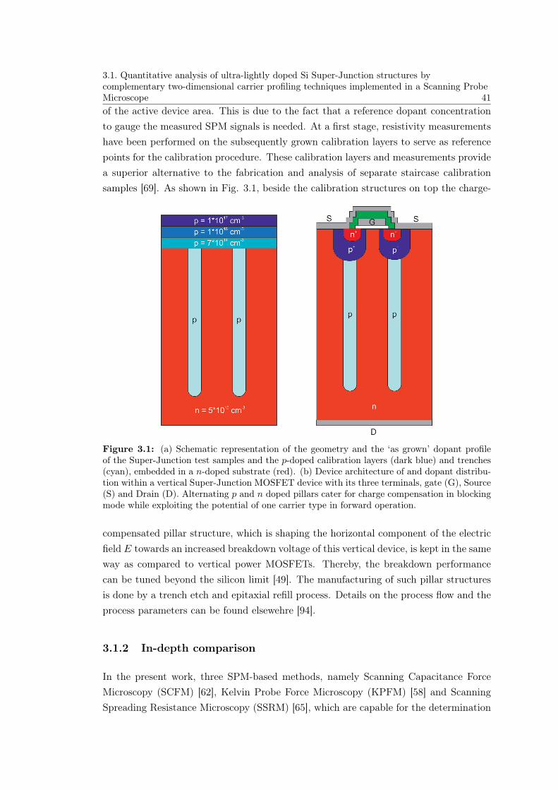
3.1. Quantitative analysis of ultra-lightly doped Si Super-Junction structures bycomplementary two-dimensional carrier profiling techniques implemented in a Scanning ProbeMicroscope 41of the active device area. This is due to the fact that a reference dopant concentrationto gauge the measured SPM signals is needed. At a first stage, resistivity measurementshave been performed on the subsequently grown calibration layers to serve as referencepoints for the calibration procedure. These calibration layers and measurements providea superior alternative to the fabrication and analysis of separate staircase calibrationsamples [69]. As shown in Fig. 3.1, beside the calibration structures on top the charge-
Figure 3.1: (a) Schematic representation of the geometry and the ‘as grown’ dopant profileof the Super-Junction test samples and the p-doped calibration layers (dark blue) and trenches(cyan), embedded in a n-doped substrate (red). (b) Device architecture of and dopant distribu-tion within a vertical Super-Junction MOSFET device with its three terminals, gate (G), Source(S) and Drain (D). Alternating p and n doped pillars cater for charge compensation in blockingmode while exploiting the potential of one carrier type in forward operation.
compensated pillar structure, which is shaping the horizontal component of the electricfield E towards an increased breakdown voltage of this vertical device, is kept in the sameway as compared to vertical power MOSFETs. Thereby, the breakdown performancecan be tuned beyond the silicon limit [49]. The manufacturing of such pillar structuresis done by a trench etch and epitaxial refill process. Details on the process flow and theprocess parameters can be found elsewehre [94].
3.1.2 In-depth comparison
In the present work, three SPM-based methods, namely Scanning Capacitance ForceMicroscopy (SCFM) [62], Kelvin Probe Force Microscopy (KPFM) [58] and ScanningSpreading Resistance Microscopy (SSRM) [65], which are capable for the determination
42 Chapter 3. Low dopant regime carrier profiling by SPM methods
of carrier profiles, i.e. electronically active dopant profiles, at low concentrations havebeen selected and incorporated in the same measurement system for an in-depth com-parison. Importantly also, to rule out artefacts originating from the sample preparationprocedure, the same scheme has been employed in the preparation of the specimensprobed by all three methods. The specific scheme has been defined consequent to theexamination of several different preparation approaches for the sample cross-section. Wefound that the chemical mechanical polishing (CMP) process achieved the best resultsin terms of a low surface roughness (below 1 nm, as shown in fig. 3.2a) and resulted ina low density of surface states. The latter is needed to avoid the pinning of the Fermilevels of the probing sensor-tip and the sample and is most important to allow for quan-titative Contact Potential Difference (CPD) measurements representing the 3D (bulk,i.e. not surface modified) properties of the material below the surface cross-section.The topographic images, like the one shown in Fig. 3.2a were acquired simultaneously
Figure 3.2: (a) Simultaneously acquired topographic images while either KPFM (b) or SCFM(c) measurements were performed by the oscillation of the second eigenmode. (c) As the surfaceis modified by measurements in contact mode, SSRM measurements (d) were always performedat the end of each measurement sequence and on each specimen. Figure adapted from unpub-lished AFM data by U. Gysin.
to the corresponding dopant map. SSRM, unlike the other, non-contact force detectingmicroscopy techniques, involves scanning the specimen in contact mode while the lat-ter detect forces by measuring the modification of a higher harmonic of the cantileverresonance frequency in general and also when applied for dopant profiling [95]. As canbe seen in Fig. 3.2a, there are no topographic features visible in either dopant imagingtechnique which correspond to the faintly visible features in the topography channel. Itis therefore concluded that the sample preparation as established is successful in pro-ducing sufficiently flat specimens and the nature of the physical contrast (Fig. 3.2b-d)is attributed to a pure dopant effect. The analysis of the sensitivity of each method and

3.1. Quantitative analysis of ultra-lightly doped Si Super-Junction structures bycomplementary two-dimensional carrier profiling techniques implemented in a Scanning ProbeMicroscope 43comparison to the theory is complex since there are a variety of effects which complicatequantitative dopant profiling. Starting with KPFM, the lowest p dopant concentrationdifference of the first two calibration layers is exactly one order of magnitude (see Fig.3.1a). According to the formula for the CPD difference between two layers,
∆V 1−2CDP =
kBT
qlnN1A
N2A
(3.1)
where kB is the Boltzmann constant, T is the temperature, q is the elementary chargeand N1,2
A are the acceptor densities, two plateaus should be visible in the dopant mapwith 60 mV height difference at room temperature. Since the calibration layers couldbe clearly resolved (see Fig. 3.2c) it can be considered that the resolution for dopantdetection and quantification is below this value. While this method can only be uti-lized for relative dopant profiling of differently doped areas, KPFM in principle alsoprovides a tool to directly quantify concentration values if the work function of the tipis well known. However, the corresponding formula is not generally applicable due tothe strong influence of defect states on the band structure. Even experiments performedunder defect passivating laser illumination conditions have shown that the conductionand valence bands are bent towards each other, therefore resulting in an underestimatedbuilt-in voltage across the pn junction.The theoretical relative value of 127 mV for the CPD between the two outmost cali-bration layers is not in good agreement with the experimental values of 332 mV. Thisis attributed to the high surface sensitivity of a few nanometers of the Kelvin probemethod, which pronounces features at the surface like the presence of oxide layers, ad-sorbates or defects and the surface carrier density which is prone to modifications bydopant depletion. The ‘surface bias’ of KPFM relates to the non-contact measurementwhere the average tip-sample separation is comparable to the information depth. Whilealso comprising a non-contact SPM technique SCFM operates in a different cantileverfrequency range and utilizes a very different physical quantity utilized for mapping thedopant concentration. The working principle of SCFM is similar to Scanning Capac-itance Microscopy (SCM) [96] with the difference that the capacitive response to anexternal electric stimulus is detected via the interaction force which is modifying thecantilever oscillation and not electrically as it is the case for SCM [97]. The read outof the amplitude and phase signal from SCFM measurements which can be related tothe dopant concentration is carried out by a lock-in amplifier that is able to separatelyaddress the 3ω component of the electrostatic force [62]. It is interesting to note thatthe change of the depletion layer capacitance signal with respect to an AC bias voltage islarger for smaller doping concentrations. This characteristic makes this method an idealcandidate for the investigation of power devices with their lightly doped drift layers. ForSCFM the information depth can be estimated by the maximal depletion layer width
44 Chapter 3. Low dopant regime carrier profiling by SPM methods
[34]
WD,max =
√4εskT ln(NA
ni)
q2NA(3.2)
where εs is the permittivity of the semiconductor and ni is the intrinsic carrier density.The information depth, in contrast to KPFM, is much larger and critically depends onthe dopant concentration. The corresponding maximum depletion layer widths of thethree calibration layers used in this study starting from the topmost layer are 100 nm,300 nm and 1000 nm. Hence the relatively small tip-sample separation (v 10 nm) andthe thin oxide layer do not significantly deteriorate the measurement signal arising formfrom the subsurface semiconducting material.The third method for mapping dopant concentrations that has been used for the presentcomparison is SSRM. In contrary to the other two techniques the carrier density is mea-sured via resistance changes by the means of a current measurement in contact mode.The main advantage of this approach is its ruggedness with respect to variations in thesample preparation routine due to its self preparing nature. During the measurement,significant forces are exerted by the tip to maintain the current. Hence, the progressivescanning of the same surface area leads to a removal of less conductive surface layers.Thereby the measured spreading resistance after some frames corresponds to a freshlyexposed surface and slower depletion and defect accumulation mechanisms do not playa role. On the other hand this strength of SSRM is accompanied by the destruction ofthe sample, as the surface gets locally etched during the measurement. Compared to themore elegant non-contact techniques that work well under certain experimental condi-tions but either suffer from preparation induced defects or a less advanced quantificationpotential, SSRM shows a high reproducibility not only from a qualitative but also froma quantitative perspective. The details of the quantification procedure are following inthe next section.
3.1.3 Conclusions
The ability of three different carrier profiling methods that are incorporated in a custom-built AFM system have been assessed in terms of their quantification potential using theexample of lightly doped Si Super-Junction test structures. It has been demonstratedthat both, non-contact (SCFM, KPFM) and contact mode techniques (SSRM), exhibitan unprecedented sensitivity to map electronically active dopant profiles with concen-trations starting form as low as 1014 cm-3. Depending on the physical quantity that ismeasured and in the nature of the employed technique however, differences in the resolu-tion as well as in the quantification capability have been observed. The surface potentialmeasurement as it is applied in KPFM is the most surface sensitive technique and getstherefore more easily distorted by preparation induced defects and surface adsorbates.
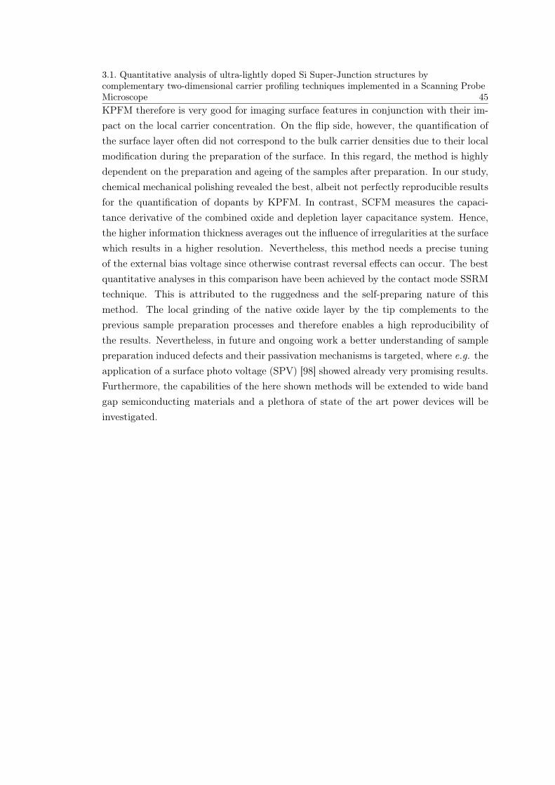
3.1. Quantitative analysis of ultra-lightly doped Si Super-Junction structures bycomplementary two-dimensional carrier profiling techniques implemented in a Scanning ProbeMicroscope 45KPFM therefore is very good for imaging surface features in conjunction with their im-pact on the local carrier concentration. On the flip side, however, the quantification ofthe surface layer often did not correspond to the bulk carrier densities due to their localmodification during the preparation of the surface. In this regard, the method is highlydependent on the preparation and ageing of the samples after preparation. In our study,chemical mechanical polishing revealed the best, albeit not perfectly reproducible resultsfor the quantification of dopants by KPFM. In contrast, SCFM measures the capaci-tance derivative of the combined oxide and depletion layer capacitance system. Hence,the higher information thickness averages out the influence of irregularities at the surfacewhich results in a higher resolution. Nevertheless, this method needs a precise tuningof the external bias voltage since otherwise contrast reversal effects can occur. The bestquantitative analyses in this comparison have been achieved by the contact mode SSRMtechnique. This is attributed to the ruggedness and the self-preparing nature of thismethod. The local grinding of the native oxide layer by the tip complements to theprevious sample preparation processes and therefore enables a high reproducibility ofthe results. Nevertheless, in future and ongoing work a better understanding of samplepreparation induced defects and their passivation mechanisms is targeted, where e.g. theapplication of a surface photo voltage (SPV) [98] showed already very promising results.Furthermore, the capabilities of the here shown methods will be extended to wide bandgap semiconducting materials and a plethora of state of the art power devices will beinvestigated.
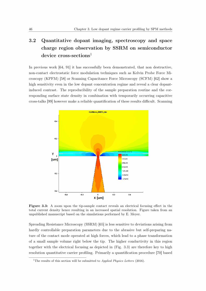
46 Chapter 3. Low dopant regime carrier profiling by SPM methods
3.2 Quantitative dopant imaging, spectroscopy and spacecharge region observation by SSRM on semiconductordevice cross-sections1
In previous work [64, 91] it has successfully been demonstrated, that non destructive,non-contact electrostatic force modulation techniques such as Kelvin Probe Force Mi-croscopy (KPFM) [58] or Scanning Capacitance Force Microscopy (SCFM) [62] show ahigh sensitivity even in the low dopant concentration regime and reveal a clear dopant-induced contrast. The reproducibility of the sample preparation routine and the cor-responding surface state density in combination with temporarily occurring capacitivecross-talks [99] however make a reliable quantification of these results difficult. Scanning
Figure 3.3: A zoom upon the tip-sample contact reveals an electrical focusing effect in thetotal current density hence resulting in an increased spatial resolution. Figure taken from anunpublished manuscript based on the simulations performed by E. Meyer.
Spreading Resistance Microscopy (SSRM) [65] is less sensitive to deviations arising fromhardly controllable preparation parameters due to the abrasive but self-preparing na-ture of the contact mode operated at high forces, which lead to a phase transformationof a small sample volume right below the tip. The higher conductivity in this regiontogether with the electrical focusing as depicted in (Fig. 3.3) are therefore key to highresolution quantitative carrier profiling. Primarily a quantification procedure [70] based
1The results of this section will be submitted to Applied Physics Letters (2016).
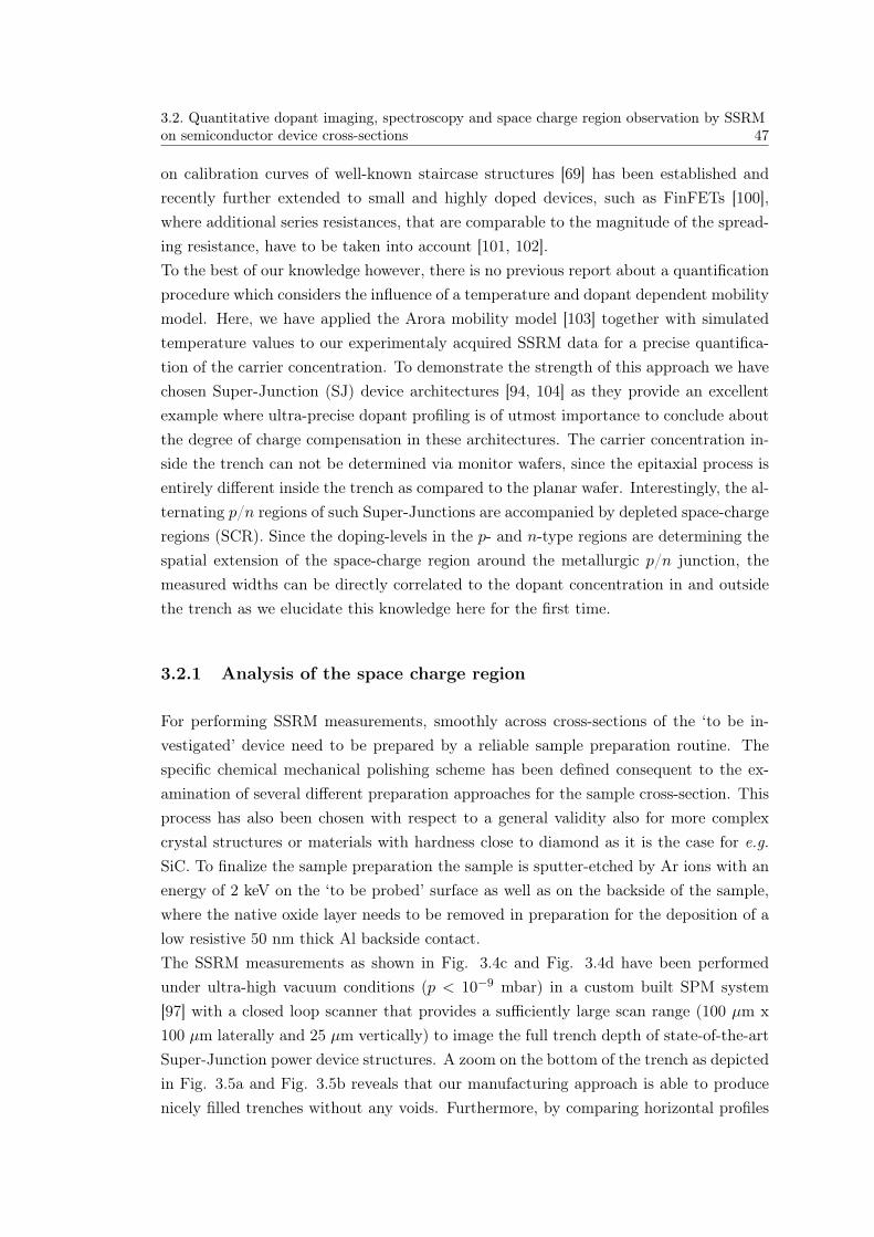
3.2. Quantitative dopant imaging, spectroscopy and space charge region observation by SSRMon semiconductor device cross-sections 47
on calibration curves of well-known staircase structures [69] has been established andrecently further extended to small and highly doped devices, such as FinFETs [100],where additional series resistances, that are comparable to the magnitude of the spread-ing resistance, have to be taken into account [101, 102].To the best of our knowledge however, there is no previous report about a quantificationprocedure which considers the influence of a temperature and dopant dependent mobilitymodel. Here, we have applied the Arora mobility model [103] together with simulatedtemperature values to our experimentaly acquired SSRM data for a precise quantifica-tion of the carrier concentration. To demonstrate the strength of this approach we havechosen Super-Junction (SJ) device architectures [94, 104] as they provide an excellentexample where ultra-precise dopant profiling is of utmost importance to conclude aboutthe degree of charge compensation in these architectures. The carrier concentration in-side the trench can not be determined via monitor wafers, since the epitaxial process isentirely different inside the trench as compared to the planar wafer. Interestingly, the al-ternating p/n regions of such Super-Junctions are accompanied by depleted space-chargeregions (SCR). Since the doping-levels in the p- and n-type regions are determining thespatial extension of the space-charge region around the metallurgic p/n junction, themeasured widths can be directly correlated to the dopant concentration in and outsidethe trench as we elucidate this knowledge here for the first time.
3.2.1 Analysis of the space charge region
For performing SSRM measurements, smoothly across cross-sections of the ‘to be in-vestigated’ device need to be prepared by a reliable sample preparation routine. Thespecific chemical mechanical polishing scheme has been defined consequent to the ex-amination of several different preparation approaches for the sample cross-section. Thisprocess has also been chosen with respect to a general validity also for more complexcrystal structures or materials with hardness close to diamond as it is the case for e.g.SiC. To finalize the sample preparation the sample is sputter-etched by Ar ions with anenergy of 2 keV on the ‘to be probed’ surface as well as on the backside of the sample,where the native oxide layer needs to be removed in preparation for the deposition of alow resistive 50 nm thick Al backside contact.The SSRM measurements as shown in Fig. 3.4c and Fig. 3.4d have been performedunder ultra-high vacuum conditions (p < 10−9 mbar) in a custom built SPM system[97] with a closed loop scanner that provides a sufficiently large scan range (100 µm x100 µm laterally and 25 µm vertically) to image the full trench depth of state-of-the-artSuper-Junction power device structures. A zoom on the bottom of the trench as depictedin Fig. 3.5a and Fig. 3.5b reveals that our manufacturing approach is able to producenicely filled trenches without any voids. Furthermore, by comparing horizontal profiles
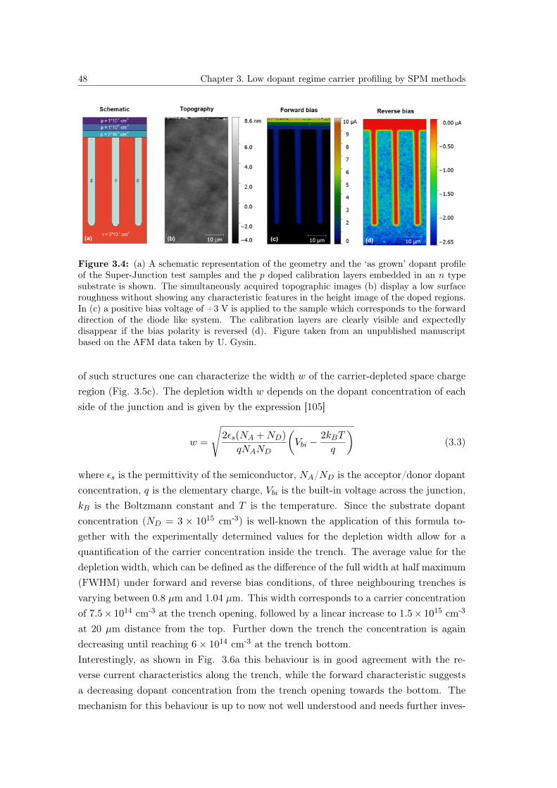
48 Chapter 3. Low dopant regime carrier profiling by SPM methods
Figure 3.4: (a) A schematic representation of the geometry and the ‘as grown’ dopant profileof the Super-Junction test samples and the p doped calibration layers embedded in an n typesubstrate is shown. The simultaneously acquired topographic images (b) display a low surfaceroughness without showing any characteristic features in the height image of the doped regions.In (c) a positive bias voltage of +3 V is applied to the sample which corresponds to the forwarddirection of the diode like system. The calibration layers are clearly visible and expectedlydisappear if the bias polarity is reversed (d). Figure taken from an unpublished manuscriptbased on the AFM data taken by U. Gysin.
of such structures one can characterize the width w of the carrier-depleted space chargeregion (Fig. 3.5c). The depletion width w depends on the dopant concentration of eachside of the junction and is given by the expression [105]
w =
√2εs(NA +ND)
qNAND
(Vbi −
2kBT
q
)(3.3)
where εs is the permittivity of the semiconductor, NA/ND is the acceptor/donor dopantconcentration, q is the elementary charge, Vbi is the built-in voltage across the junction,kB is the Boltzmann constant and T is the temperature. Since the substrate dopantconcentration (ND = 3 × 1015 cm-3) is well-known the application of this formula to-gether with the experimentally determined values for the depletion width allow for aquantification of the carrier concentration inside the trench. The average value for thedepletion width, which can be defined as the difference of the full width at half maximum(FWHM) under forward and reverse bias conditions, of three neighbouring trenches isvarying between 0.8 µm and 1.04 µm. This width corresponds to a carrier concentrationof 7.5× 1014 cm-3 at the trench opening, followed by a linear increase to 1.5× 1015 cm-3
at 20 µm distance from the top. Further down the trench the concentration is againdecreasing until reaching 6× 1014 cm-3 at the trench bottom.Interestingly, as shown in Fig. 3.6a this behaviour is in good agreement with the re-verse current characteristics along the trench, while the forward characteristic suggestsa decreasing dopant concentration from the trench opening towards the bottom. Themechanism for this behaviour is up to now not well understood and needs further inves-

3.2. Quantitative dopant imaging, spectroscopy and space charge region observation by SSRMon semiconductor device cross-sections 49
Figure 3.5: The technologically most relevant region at the trench bottom is shown. At apositive bias voltage current is conducted through the p-pillars (a). If the bias polarity getsreversed, the n-type substrate becomes conductive. A comparison of horizontal profiles forthese two configurations allows for drawing conclusions on the width of the space charge region,which later on can be related to the carrier concentration inside the trench. The hole currenthas thereby been multiplied by a factor of three due to the reduced hole mobility. Figures takenfrom an unpublished manuscript based on the AFM data taken by U. Gysin.
tigation. From a fabrication and preparation perspective it is suggested that the trenchopening exhibits a higher dopant concentration since it is rather intuitive that dopantsare more easily incorporated there. The polishing with Al2O3 particles could also intro-duce additional acceptor impurities. On the other hand also dopant out-diffusion cantake place during the polishing process.
3.2.2 Quantification by means of the Arora mobility model
Beside the analysis of the space charge region that develops at the boundary betweenp and n-doped pillars a quantification based on the Arora mobility model [103] hasbeen investigated. In contrast to other mobility models the Arora model takes a dopantand temperature dependent mobility into account which needs to be considered in in-termediate dopant concentration regimes. For the limiting cases of very high or verylow concentrations the mobility is either determined by impurity scattering or phononscattering. The hole mobility according to the Aroroa model is given by the expression[103]
µh = 54.3T−0.57n +
1.36× 10⁸T−2.23
1 + [N/(2.35× 1017T 2.4n )]0.88T−0.146
n
(3.4)
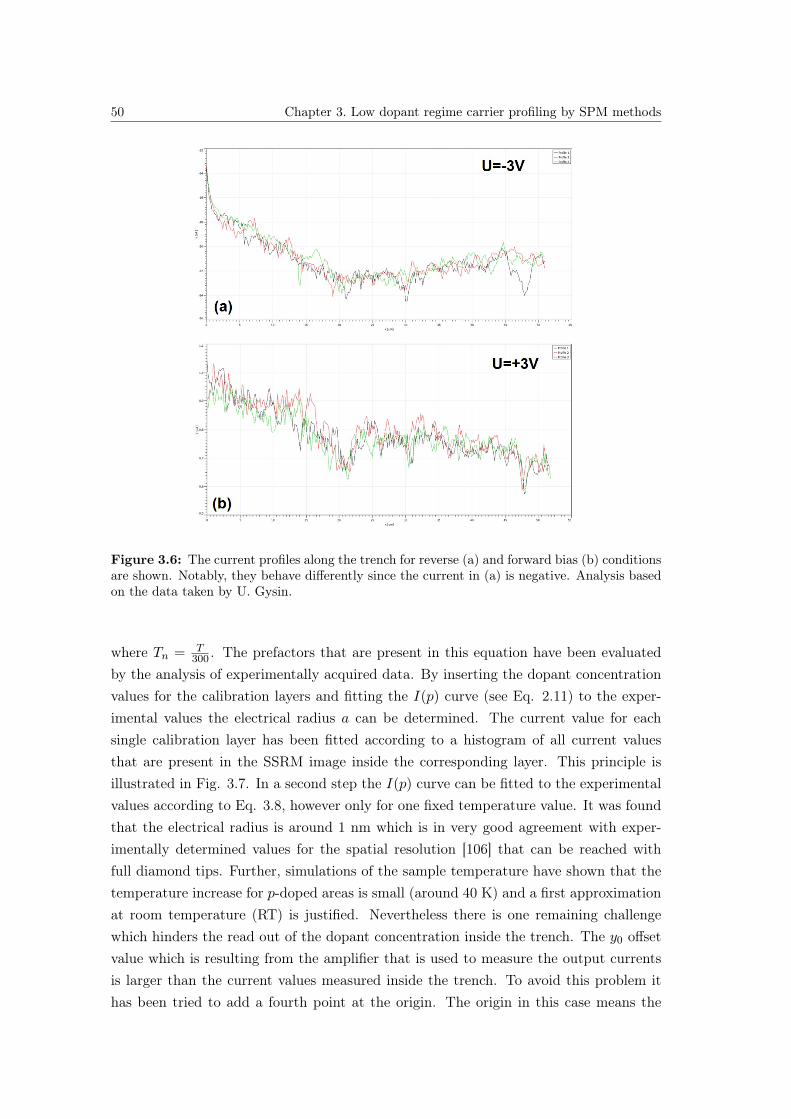
50 Chapter 3. Low dopant regime carrier profiling by SPM methods
Figure 3.6: The current profiles along the trench for reverse (a) and forward bias (b) conditionsare shown. Notably, they behave differently since the current in (a) is negative. Analysis basedon the data taken by U. Gysin.
where Tn = T300 . The prefactors that are present in this equation have been evaluated
by the analysis of experimentally acquired data. By inserting the dopant concentrationvalues for the calibration layers and fitting the I(p) curve (see Eq. 2.11) to the exper-imental values the electrical radius a can be determined. The current value for eachsingle calibration layer has been fitted according to a histogram of all current valuesthat are present in the SSRM image inside the corresponding layer. This principle isillustrated in Fig. 3.7. In a second step the I(p) curve can be fitted to the experimentalvalues according to Eq. 3.8, however only for one fixed temperature value. It was foundthat the electrical radius is around 1 nm which is in very good agreement with exper-imentally determined values for the spatial resolution [106] that can be reached withfull diamond tips. Further, simulations of the sample temperature have shown that thetemperature increase for p-doped areas is small (around 40 K) and a first approximationat room temperature (RT) is justified. Nevertheless there is one remaining challengewhich hinders the read out of the dopant concentration inside the trench. The y0 offsetvalue which is resulting from the amplifier that is used to measure the output currentsis larger than the current values measured inside the trench. To avoid this problem ithas been tried to add a fourth point at the origin. The origin in this case means the
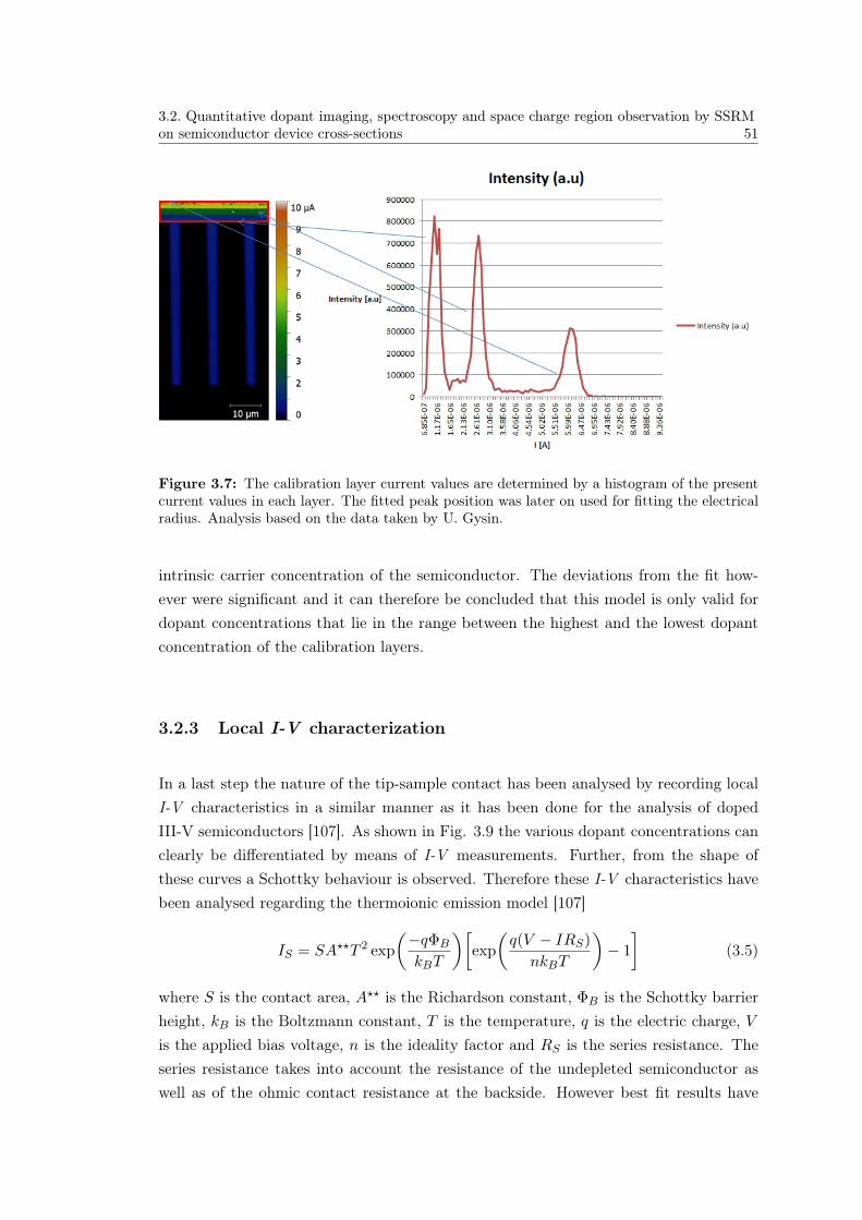
3.2. Quantitative dopant imaging, spectroscopy and space charge region observation by SSRMon semiconductor device cross-sections 51
Figure 3.7: The calibration layer current values are determined by a histogram of the presentcurrent values in each layer. The fitted peak position was later on used for fitting the electricalradius. Analysis based on the data taken by U. Gysin.
intrinsic carrier concentration of the semiconductor. The deviations from the fit how-ever were significant and it can therefore be concluded that this model is only valid fordopant concentrations that lie in the range between the highest and the lowest dopantconcentration of the calibration layers.
3.2.3 Local I-V characterization
In a last step the nature of the tip-sample contact has been analysed by recording localI-V characteristics in a similar manner as it has been done for the analysis of dopedIII-V semiconductors [107]. As shown in Fig. 3.9 the various dopant concentrations canclearly be differentiated by means of I-V measurements. Further, from the shape ofthese curves a Schottky behaviour is observed. Therefore these I-V characteristics havebeen analysed regarding the thermoionic emission model [107]
IS = SA??T 2 exp
(−qΦB
kBT
)[exp
(q(V − IRS)
nkBT
)− 1
](3.5)
where S is the contact area, A?? is the Richardson constant, ΦB is the Schottky barrierheight, kB is the Boltzmann constant, T is the temperature, q is the electric charge, Vis the applied bias voltage, n is the ideality factor and RS is the series resistance. Theseries resistance takes into account the resistance of the undepleted semiconductor aswell as of the ohmic contact resistance at the backside. However best fit results have
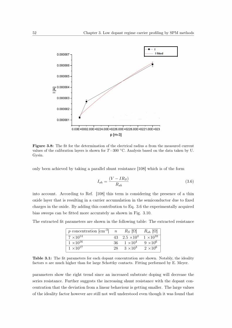
52 Chapter 3. Low dopant regime carrier profiling by SPM methods
Figure 3.8: The fit for the determination of the electrical radius a from the measured currentvalues of the calibration layers is shown for T=300 C. Analysis based on the data taken by U.Gysin.
only been achieved by taking a parallel shunt resistance [108] which is of the form
Ish =(V − IRS)
Rsh(3.6)
into account. According to Ref. [108] this term is considering the presence of a thinoxide layer that is resulting in a carrier accumulation in the semiconductor due to fixedcharges in the oxide. By adding this contribution to Eq. 3.6 the experimentally acquiredbias sweeps can be fitted more accurately as shown in Fig. 3.10.
The extracted fit parameters are shown in the following table: The extracted resistance
p concentration [cm-3] n RS [Ω] Rsh [Ω]7 ×10¹⁴ 43 2.5 ×10⁴ 1 ×10¹⁰
1 ×10¹⁶ 36 1 ×10⁴ 9 ×10⁶
1 ×10¹⁷ 28 3 ×10³ 2 ×10⁶
Table 3.1: The fit parameters for each dopant concentration are shown. Notably, the idealityfactors n are much higher than for large Schottky contacts. Fitting performed by E. Meyer.
parameters show the right trend since an increased substrate doping will decrease theseries resistance. Further suggests the increasing shunt resistance with the dopant con-centration that the deviation from a linear behaviour is getting smaller. The large valuesof the ideality factor however are still not well understood even though it was found that

3.2. Quantitative dopant imaging, spectroscopy and space charge region observation by SSRMon semiconductor device cross-sections 53
Figure 3.9: The I-V characteristics for the differently p-doped calibration layers are shown.Data recorded by U. Gysin.
point contact systems exhibit larger values for the ideality factor [109].As shown in the simulations of Fig. 3.3 there is a hole depleted surface layer present inthe proximity of the tip. In experiments on nanoscale I-V measurements it has beenreported that a surface recombination and generation current can decouple majority andminority currents [110, 111]. While the majority current is flowing across the surface theminority current is flowing along the surface and can be of a similar magnitude or evenlarger than the actual majority current that is flowing across the interface. In the casereported here the minority electron current is not dominant, however it is likely that theideality factor is nevertheless influenced.
3.2.4 Conclusions
In this section the quantification possibilities of SSRM measurements have been ad-dressed based on two different methods. On the one hand the alternating pillar structuregives rise to a space charge region at the pn junction which can be quantified by thecomparison of vertical profiles along the recorded SSRM images under forward and re-verse bias. Due to the low dopant concentration inside the trench of the Super-Junctionarchitecture an extended space-charge region could be observed whereof a large fractionis inside the carrier depleted trench.On the other hand a quantification procedure based on the Arora mobility model hasbeen introduced. By the use of three layers of well-known dopant concentration the

54 Chapter 3. Low dopant regime carrier profiling by SPM methods
Figure 3.10: The experimentally acquired I-V data is shown up to a bias voltage of 5 V andcompared to the corresponding fit that is taking a series and parallel resistance into account.Analysis performed by E. Meyer.
measured current could be fitted as a function of the dopant concentration. The impactof Joule heating has been simulated and was found to be small, which justified a firstapproximation at RT. The electrical radius a and the y0 offset due to the used amplifierfor the current measurement were thereby the only fit parameters and the electrical ra-dius was in good agreement with the literature.At this point however it is hard to judge which method shall be preferred in termsof the quantification of dopant profiles inside the trench since further challenges needto be overcome. While for the first method the correlation of the width of the SCRalong the trench and the corresponding current profiles needs further investigation thesecond method was currently suffering from an inappropriate choice of the dopant con-centrations of the calibration layers. Also attention has to be paid on the nature of thetip-sample contact which is showing rather a Schottky than an ohmic behaviour. Forthis nanoscale Schottky contacts so far the best agreement between the experimentaland theoretical values has been achieved by considering a parallel shunt resistance thattake the presence of a thin oxide layer with fixed positive charges into account. Thehigh ideality factors might be caused by minority electron currents that spread alongthe surface and influence the I-V characteristics across the contact itself.
CHAPTER 4
Characterization of active device areas in 4H-SiC
Within this chapter electronically active dopant profiles of epitaxially grown n-type 4H-SiC calibration layer structures with dopant concentrations ranging from 3× 1015 cm-3
to 1 × 1019 cm-3 have been investigated by non-contact Scanning Probe Microscopy(SPM) methods. It has been shown that Kelvin Probe Force Microscopy (KPFM) andElectrostatic Force Microscopy (EFM) are capable of resolving two-dimensional carriermaps in the low doping concentration regime with high spatial resolution. Furthermore,different information depths of this wide band gap semiconductor material could beassessed due to the inherent properties of each profiling method. Additionally a resolu-tion enhancement has been observed under laser illumination which was attributed toreduced band-bending conditions. To gauge the SPM signals, epitaxially grown layerswere primarily calibrated in terms of their dopant concentration by C-V measurements.Further, the shielding cell-architecture of a buried grid (BG) Junction Barrier Schottky(JBS) diode consisting of multiple consecutive p+-implanted stripes below the interfaceof the metal/semiconductor junction has been investigated by performing non-contactScanning Probe Microscopy (SPM) and Secondary Electron Potential Contrast (SEPC)measurements on device cross-sections. It has been shown that these techniques arecapable of mapping two-dimensional (2D) carrier distributions inside the active devicearea, however with different resolution and quantification possibilities.
55
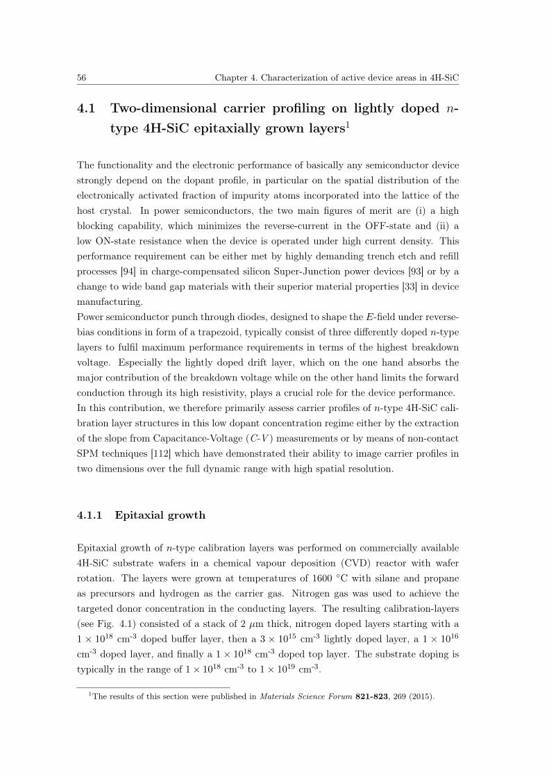
56 Chapter 4. Characterization of active device areas in 4H-SiC
4.1 Two-dimensional carrier profiling on lightly doped n-type 4H-SiC epitaxially grown layers1
The functionality and the electronic performance of basically any semiconductor devicestrongly depend on the dopant profile, in particular on the spatial distribution of theelectronically activated fraction of impurity atoms incorporated into the lattice of thehost crystal. In power semiconductors, the two main figures of merit are (i) a highblocking capability, which minimizes the reverse-current in the OFF-state and (ii) alow ON-state resistance when the device is operated under high current density. Thisperformance requirement can be either met by highly demanding trench etch and refillprocesses [94] in charge-compensated silicon Super-Junction power devices [93] or by achange to wide band gap materials with their superior material properties [33] in devicemanufacturing.Power semiconductor punch through diodes, designed to shape the E-field under reverse-bias conditions in form of a trapezoid, typically consist of three differently doped n-typelayers to fulfil maximum performance requirements in terms of the highest breakdownvoltage. Especially the lightly doped drift layer, which on the one hand absorbs themajor contribution of the breakdown voltage while on the other hand limits the forwardconduction through its high resistivity, plays a crucial role for the device performance.In this contribution, we therefore primarily assess carrier profiles of n-type 4H-SiC cali-bration layer structures in this low dopant concentration regime either by the extractionof the slope from Capacitance-Voltage (C-V ) measurements or by means of non-contactSPM techniques [112] which have demonstrated their ability to image carrier profiles intwo dimensions over the full dynamic range with high spatial resolution.
4.1.1 Epitaxial growth
Epitaxial growth of n-type calibration layers was performed on commercially available4H-SiC substrate wafers in a chemical vapour deposition (CVD) reactor with waferrotation. The layers were grown at temperatures of 1600 C with silane and propaneas precursors and hydrogen as the carrier gas. Nitrogen gas was used to achieve thetargeted donor concentration in the conducting layers. The resulting calibration-layers(see Fig. 4.1) consisted of a stack of 2 µm thick, nitrogen doped layers starting with a1 × 1018 cm-3 doped buffer layer, then a 3 × 1015 cm-3 lightly doped layer, a 1 × 10¹⁶
cm-3 doped layer, and finally a 1× 1018 cm-3 doped top layer. The substrate doping istypically in the range of 1× 1018 cm-3 to 1× 1019 cm-3.
1The results of this section were published in Materials Science Forum 821-823, 269 (2015).
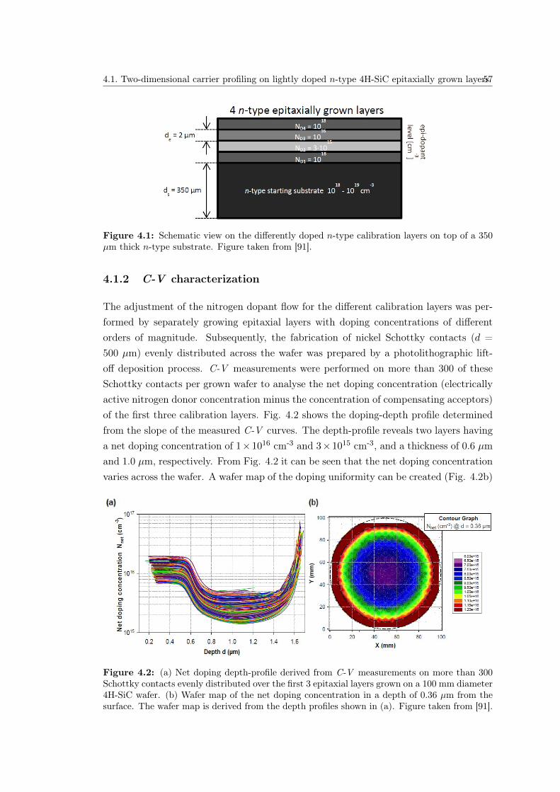
4.1. Two-dimensional carrier profiling on lightly doped n-type 4H-SiC epitaxially grown layers57
Figure 4.1: Schematic view on the differently doped n-type calibration layers on top of a 350µm thick n-type substrate. Figure taken from [91].
4.1.2 C-V characterization
The adjustment of the nitrogen dopant flow for the different calibration layers was per-formed by separately growing epitaxial layers with doping concentrations of differentorders of magnitude. Subsequently, the fabrication of nickel Schottky contacts (d =500 µm) evenly distributed across the wafer was prepared by a photolithographic lift-off deposition process. C-V measurements were performed on more than 300 of theseSchottky contacts per grown wafer to analyse the net doping concentration (electricallyactive nitrogen donor concentration minus the concentration of compensating acceptors)of the first three calibration layers. Fig. 4.2 shows the doping-depth profile determinedfrom the slope of the measured C-V curves. The depth-profile reveals two layers havinga net doping concentration of 1×1016 cm-3 and 3×1015 cm-3, and a thickness of 0.6 µmand 1.0 µm, respectively. From Fig. 4.2 it can be seen that the net doping concentrationvaries across the wafer. A wafer map of the doping uniformity can be created (Fig. 4.2b)
Figure 4.2: (a) Net doping depth-profile derived from C-V measurements on more than 300Schottky contacts evenly distributed over the first 3 epitaxial layers grown on a 100 mm diameter4H-SiC wafer. (b) Wafer map of the net doping concentration in a depth of 0.36 µm from thesurface. The wafer map is derived from the depth profiles shown in (a). Figure taken from [91].

58 Chapter 4. Characterization of active device areas in 4H-SiC
by extracting the net doping concentration at a certain depth of the profile and plot itas a function of the Schottky contact position. Due to the rotation of the wafer duringthe growth process, the doping uniformity exhibits a rotational symmetry. In our case,the center circular area with 80 mm diameter (10 mm edge exclusion) has an average netdoping concentration of 8.47×1015 cm-3 at a depth of 0.36 µm and a standard deviationover mean uniformity of 12% (Dopant range: 7.14× 10¹⁵ − 10.51× 1015 cm-3).
4.1.3 SPM-Based two-dimensional carrier profiling
The working principle of KPFM [58] and EFM [90] is based on their sensitivity todifferent electrostatic force components with differing characteristic information depthswhich arise under the influence of an external bias voltage V = VDC + VAC × sin(ωt)
between the tip and the sample:
Fω = −∂C∂z
(VDC − VCPD)VAC sin(ωt) (4.1)
F2ω =∂C
∂z
V 2AC
4cos(2ωt) (4.2)
Due to the variety of different possible cleaving planes in 4H-SiC, cross-sections wereprepared by a grinding step followed by chemical mechanical polishing with diamond par-ticles in different grain sizes and a Syton SF1 finish, which resulted in a sub-nanometersurface roughness (Fig. 4.3a).Nevertheless, as shown in Fig. 4.3b, fine scratches due to our preparation method stillremain visible in the compensating DC bias image influencing the measured values forthe Contact Potential Difference (CPD), while in the amplitude signal of the EFM image(Fig. 4.3c) this effect gets less pronounced. This can be attributed to the influence ofthe capacitance variation on the different force components. Since for KPFM measure-ments the CPD gets compensated by an external DC bias, the Fω force component (Eq.4.1) vanishes and with it the influence of changes in the capacitance signal. In contrast,the response of the semiconductor material to the oscillating term by the external biasvoltage induces periodic accumulation and depletion of free charge carriers resulting ina variable depletion layer capacitance. Hence, the amplitude of the F2ω component (Eq.4.2) is probing rather extended depletion layers, whereas KPFM is very sensitive to sur-face defects and adsorbates.Our measurements were performed under ultra-high vacuum (UHV) conditions, whichenabled us to simultaneously acquire topographic images (Fig. 4.3a), due to the highQ-factor of the first and second resonance frequency of the PtIr-coated NanosensorsPPP-NCLPt cantilever optimized for dynamic mode operation. Further details on theexperimental setup are published elsewhere [97]. Since there are no topographic featuresvisible, we attribute the nature of the physical contrast (Fig. 4.3b,c) to a pure dopant

4.1. Two-dimensional carrier profiling on lightly doped n-type 4H-SiC epitaxially grown layers59
Figure 4.3: Simultaneously acquired topographic image (a) while KPFM (b) and 2ω EFM (c)measurements were performed by the oscillation of the second eigenmode. To avoid roundingeffects at the sample edges two samples were glued together with non-conductive epoxy. Figuretaken from [91].
effect. In KPFM, the measured CPD = (Φs − Φt)/q allows for drawing conclusionsabout the dopant dependent work function of the inspected sample, while in EFM, thecharge carrier concentration of the sample affects the magnitude of the amplitude signal.Differences between the second (ND2 = 3× 1015 cm -3) and the third (ND3 = 1 × 10¹⁶
cm -3) epitaxially grown calibration layer corresponding to a calculated ∆CPD ≈ 31
mV could be resolved.Still, the transition region in the KPFM image (Fig. 4.3b) gets smeared out due tosurface defects, which makes it difficult to determine the position of the metallurgicaljunction. This effect can be illustrated in the energy band diagram (Fig. 4.4a) of thetip-semiconductor system. Defect states within the band gap influence the position ofthe Fermi level resulting in an increased sample work function. However, almost idealflatband conditions (Fig. 4.4b) can be restored by illuminating the sample with laserlight (λ = 500 nm with 50 nm bandwidth, 2.5 W/cm2 intensity). The diffusion of photo-generated electron-hole pairs towards the surface creates a Surface Photo Voltage (SPV)[98], which counteracts the defect-induced work function increase. As can be seen in theKPFM image of the same structure under illumination (Fig. 4.4c) a significant contrastenhancement especially at the border between two differently doped layers was achieveddue to the interaction with laser light.

60 Chapter 4. Characterization of active device areas in 4H-SiC
Figure 4.4: Energy band diagrams without (a) and with (b) laser illumination taken from[113]. KPFM image (c) under reduced band bending conditions. Entire figure taken from [91].
4.1.4 Conclusions
It is important to note that the influence of dopant depletion or accumulation togetherwith other surface defects needs to be controlled. Their influence here is, as demon-strated, low enough to avoid complete pinning of the Fermi level, but nevertheless com-promises the quantification of bulk dopant concentrations as measured by C-V mea-surements with low lateral resolution. In this contribution we have shown that SPMmethods such as KPFM and EFM are highly valuable complementary tools to inves-tigate low n-type dopant concentrations of 4H-SiC calibration layers with high spatialresolution. The probed physical quantity of these methods is different i.e. they involveSchottky transport, work function and capacitance measurements with different lateralresolution but also differ in their information depth. The latter is thereby restricted tosingle atomic layers in C-V measurements and KPFM and slightly less critical for EFMmeasurements. While for C-V measurements the large contact area and the nature ofthe dopant concentration extraction from the slope 1/C2(V ) minimize the contributionof surface states, in KPFM a distortion of the measurement results due to defect-inducedband bending could be overcome by the application of a SPV resulting in a passivation

4.1. Two-dimensional carrier profiling on lightly doped n-type 4H-SiC epitaxially grown layers61
of surface states and therefore in a significant enhancement of the resolution.
62 Chapter 4. Characterization of active device areas in 4H-SiC
4.2 Junction Barrier Schottky (JBS) Rectifier Interface En-gineering Facilitated by Two-Dimensional (2D) DopantImaging2
State-of-the-art energy efficient power conversion systems for traction or medium voltagedrive applications (e.g. 3.3 kV application voltage) require an energy efficient rectifiersolution. Such a technology should offer low switching losses during the reverse recoveryas well as superior static characteristics such as a low ON-state voltage drop and a lowleakage current level in the OFF-state. While SiC Schottky Barrier Diodes (SBD) areable to outperform Si p-i-n diodes in terms of switching speed due to their unipolarnature and specific ON-resistance for high breakdown voltages due to the beneficial ma-terial properties of SiC, these devices suffer from relatively large leakage currents forreverse-voltages above 1.5 kV [114]. Mainly the almost an order of magnitude higher(as compared to Si) electrical field E at the interface between the carrier-depleted wideband gap material and the Schottky-metal has an undesired impact on the shape of theSchottky barrier ΦB,n which connects the quantum mechanical energy levels of the semi-conductor and the metal. Image force induced barrier lowering [61] facilitates thermionicemission for low electric fields while Fowler-Nordheim tunneling [61, 115] is the dominantleakage mechanism at high reverse voltages close to avalanche breakdown.
4.2.1 JBS device design
The Junction Barrier Schottky (JBS) [116] architecture (Fig. 4.5) diminishes the in-fluence of the image force by employing highly doped p+-areas to effectively shield theSchottky-interface from high E-fields. The working principle of this p+-implanted gridpattern inside the drift layer can be understood as a superposition of reverse biased pnjunctions whose depletion fronts merge to sustain high cathode voltages along the wholedevice. In forward direction this design has two different effects. On the one hand due tothe suppression of Schottky-barrier lowering a metal characterized by a lower Schottky-barrier height in contact to the 4H-SiC crystal can be chosen to reduce the ON-statevoltage drop, while on the other hand an electron current can only flow between thep+-regions which leads to an increase of the specific ON-resistance.
Therefore, the trade-off between the active area consumption of these p+-grids andtheir shielding effect has been precisely analysed and optimized by means of numericalsimulations [118]. It was found that the Schottky-contact can be most effectively shieldedby narrow and deeply implanted p+-areas. In this contribution, we investigate a recentdescendant of this device architecture, namely the buried grid (BG) JBS design [119].
2The results of this section were published in Materials Science Forum 858, 497 (2016).
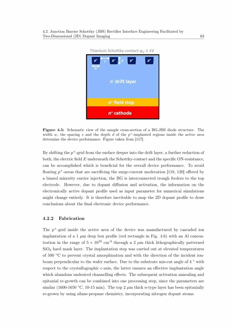
4.2. Junction Barrier Schottky (JBS) Rectifier Interface Engineering Facilitated byTwo-Dimensional (2D) Dopant Imaging 63
Figure 4.5: Schematic view of the sample cross-section of a BG-JBS diode structure. Thewidth w, the spacing s and the depth d of the p+-implanted regions inside the active areadetermine the device performance. Figure taken from [117].
By shifting the p+-grid from the surface deeper into the drift layer, a further reduction ofboth, the electric field E underneath the Schottky-contact and the specific ON-resistance,can be accomplished which is beneficial for the overall device performance. To avoidfloating p+-areas that are sacrificing the surge-current moderation [118, 120] offered bya biased minority carrier injection, the BG is interconnected trough feeders to the topelectrode. However, due to dopant diffusion and activation, the information on theelectronically active dopant profile used as input parameter for numerical simulationsmight change entirely. It is therefore inevitable to map the 2D dopant profile to drawconclusions about the final electronic device performance.
4.2.2 Fabrication
The p+-grid inside the active area of the device was manufactured by cascaded ionimplantation of a 1 µm deep box profile (red rectangle in Fig. 4.6) with an Al concen-tration in the range of 5 × 1019 cm-3 through a 2 µm thick lithographically patternedSiO2 hard mask layer. The implantation step was carried out at elevated temperaturesof 500 C to prevent crystal amorphization and with the direction of the incident ion-beam perpendicular to the wafer surface. Due to the substrate mis-cut angle of 4 withrespect to the crystallographic c-axis, the latter ensures an effective implantation anglewhich abandons undesired channelling effects. The subsequent activation annealing andepitaxial re-growth can be combined into one processing step, since the parameters aresimilar (1600-1650 C, 10-15 min). The top 2 µm thick n-type layer has been epitaxiallyre-grown by using silane-propane chemistry, incorporating nitrogen dopant atoms.
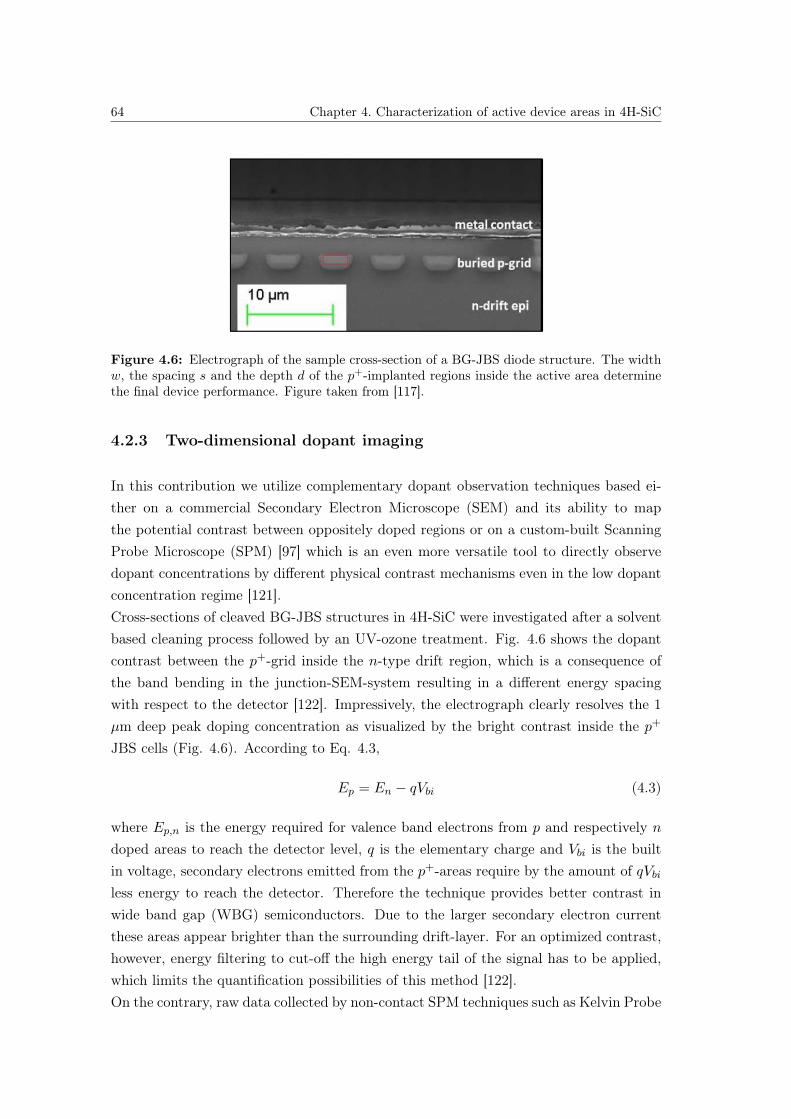
64 Chapter 4. Characterization of active device areas in 4H-SiC
Figure 4.6: Electrograph of the sample cross-section of a BG-JBS diode structure. The widthw, the spacing s and the depth d of the p+-implanted regions inside the active area determinethe final device performance. Figure taken from [117].
4.2.3 Two-dimensional dopant imaging
In this contribution we utilize complementary dopant observation techniques based ei-ther on a commercial Secondary Electron Microscope (SEM) and its ability to mapthe potential contrast between oppositely doped regions or on a custom-built ScanningProbe Microscope (SPM) [97] which is an even more versatile tool to directly observedopant concentrations by different physical contrast mechanisms even in the low dopantconcentration regime [121].Cross-sections of cleaved BG-JBS structures in 4H-SiC were investigated after a solventbased cleaning process followed by an UV-ozone treatment. Fig. 4.6 shows the dopantcontrast between the p+-grid inside the n-type drift region, which is a consequence ofthe band bending in the junction-SEM-system resulting in a different energy spacingwith respect to the detector [122]. Impressively, the electrograph clearly resolves the 1µm deep peak doping concentration as visualized by the bright contrast inside the p+
JBS cells (Fig. 4.6). According to Eq. 4.3,
Ep = En − qVbi (4.3)
where Ep,n is the energy required for valence band electrons from p and respectively ndoped areas to reach the detector level, q is the elementary charge and Vbi is the builtin voltage, secondary electrons emitted from the p+-areas require by the amount of qVbiless energy to reach the detector. Therefore the technique provides better contrast inwide band gap (WBG) semiconductors. Due to the larger secondary electron currentthese areas appear brighter than the surrounding drift-layer. For an optimized contrast,however, energy filtering to cut-off the high energy tail of the signal has to be applied,which limits the quantification possibilities of this method [122].On the contrary, raw data collected by non-contact SPM techniques such as Kelvin Probe
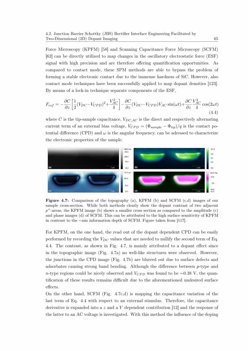
4.2. Junction Barrier Schottky (JBS) Rectifier Interface Engineering Facilitated byTwo-Dimensional (2D) Dopant Imaging 65
Force Microscopy (KPFM) [58] and Scanning Capacitance Force Microscopy (SCFM)[62] can be directly utilized to map changes in the oscillatory electrostatic force (ESF)signal with high precision and are therefore offering quantification opportunities. Ascompared to contact mode, these SPM methods are able to bypass the problem offorming a stable electronic contact due to the immense hardness of SiC. However, alsocontact mode techniques have been successfully applied to map dopant densities [123].By means of a lock-in technique separate components of the ESF,
Fesf = −∂C∂z
[1
2(VDC−VCPD)2+
V 2AC
4
]−∂C∂z
(VDC−VCPD)VAC sin(ωt)+∂C
∂z
V 2AC
4cos(2ωt)
(4.4)where C is the tip-sample capacitance, VDC,AC is the direct and respectively alternatingcurrent term of an external bias voltage, VCPD = (Φsample − Φtip)/q is the contact po-tential difference (CPD) and ω is the angular frequency, can be adressed to characterizethe electronic properties of the sample.
Figure 4.7: Comparison of the topography (a), KPFM (b) and SCFM (c,d) images of oursample cross-section. While both methods clearly show the dopant contrast of two adjacentp+-areas, the KPFM image (b) shows a smaller cross section as compared to the amplitude (c)and phase images (d) of SCFM. This can be attributed to the high surface sensitivity of KPFMin contrast to the ∼nm information depth of SCFM. Figure taken from [117].
For KPFM, on the one hand, the read out of the dopant dependent CPD can be easilyperformed by recording the VDC values that are needed to nullify the second term of Eq.4.4. The contrast, as shown in Fig. 4.7, is mainly attributed to a dopant effect sincein the topographic image (Fig. 4.7a) no well-like structures were observed. However,the junctions in the CPD image (Fig. 4.7b) are blurred out due to surface defects andadsorbates causing strong band bending. Although the difference between p-type andn-type regions could be nicely observed and VCPD was found to be ∼0.38 V, the quan-tification of these results remains difficult due to the aforementioned undesired surfaceeffects.On the other hand, SCFM (Fig. 4.7c,d) is mapping the capacitance variation of thelast term of Eq. 4.4 with respect to an external stimulus. Therefore, the capacitancederivative is expanded into a z and a V dependent contribution [12] and the response ofthe latter to an AC voltage is investigated. With this method the influence of the doping
66 Chapter 4. Characterization of active device areas in 4H-SiC
concentration upon the variable depletion layer capacitance can be studied especially inthe low doped regime, since those regions show a higher amplitude signal due to thegreater change in the capacitance derivative signal. Hence, the highly doped p+-regionsin Fig. 4.7c appear darker than the lightly doped drift layer. Interestingly, additionalfeatures at the border of our structures have been observed. The contrast of these fea-tures gets even more pronounced in the SCFM phase image which contains informationabout the dopant characteristics (n or p). According to previous studies [124], we at-tribute this effect to a bias dependent contrast reversal which is more likely to occur inWBG materials such as 4H-SiC due to their higher interfacial trap density. Similar toKPFM, SCFM is offering a quantification potential as this technique inherently involveslocal capacitance spectroscopy measurements. However, further theoretical studies arenecessary and until now a quantification is only possible by a comparison to preciselygauged calibration samples that were beforehand analyzed by C-V measurements [91].
4.2.4 Conclusions
Dopant concentration profiles are designed and manufactured to determine the elec-tronic behavior of every semiconductor device. Notably it is difficult to warrant their3D distribution within the device during manufacturing and during cyclic use. Here,SPM-derived methods allow for a unique access to dopant profiles along cross-sectionsof basically every device architecture. The present results on BG-JBS devices in SiCevidence that topographic, capacitive and surface potential contributions regarding thedopant density can be separated and analyzed. The observed differences in the reso-lution can be attributed to the underlying physical mechanism that is utilized for theobservation. While KPFM is a surface sensitive technique that critically depends on thesample preparation, SCFM is probing rather extended depletion layers, therefore aver-aging out surface-distortions induced by the sample preparation and making it a quiteattractive candidate for quantitative dopant mapping. In comparison to SEPC imagesthe two SPM signals exhibit much more quantitative results. However, for routine mea-surements to observe the profile shape, SEPC provides a quick alternative as comparedto SPM-based methods.In ongoing and future studies, the contrast mechanisms, the resolution and the feasibilityof calibrated dopant maps shall be explored. Additionally, different device segments ofdevice architectures at different stages of manufacturing and use provide very interest-ing specimens to reveal further insights into the atomistic processes in conjunction withdopant implantation and diffusion. Thus, these techniques open up new possibilitiesto investigate semiconductor and device physics down to the level of ultra-low dopantconcentrations and with nanometer scale resolution.
CHAPTER 5
On the assessment of channel mobilities in 4H-SiC trench MOSFETs
The aim of this chapter is to combine the U-MOSFET design with its U-shape trench-gate architecture which is well established in silicon technology and benefits from areduction in cell pitch size as well as from the elimination of the junction-FET regionwith the superior material properties of 4H-SiC. While current planar SiC MOSFETdevices are challenged by a high ON-state resistance caused by relatively poor channelmobilities due to different scattering processes at the 4H-SiC/insulator interface, ourhybrid approach benefits by the normal carrier injection in the inversion channel formedalong the 1120 direction which exhibits a higher channel mobility. In the followingparagraphs focus will be given on special lateral test structures which have a similar ar-chitecture as compared to vertical power devices but enable an exclusive characterizationof the channel mobility. In vertical power devices however only the total ON-resistancewhich consists of various different resistance components can be assessed. Numericalsimulations on the trench width and the gate insulator thickness have been performedto study their influence on the electronic performance. Furthermore, a brief insight onthe dry-etching process of trench structures in 4H-SiC will be given.
67
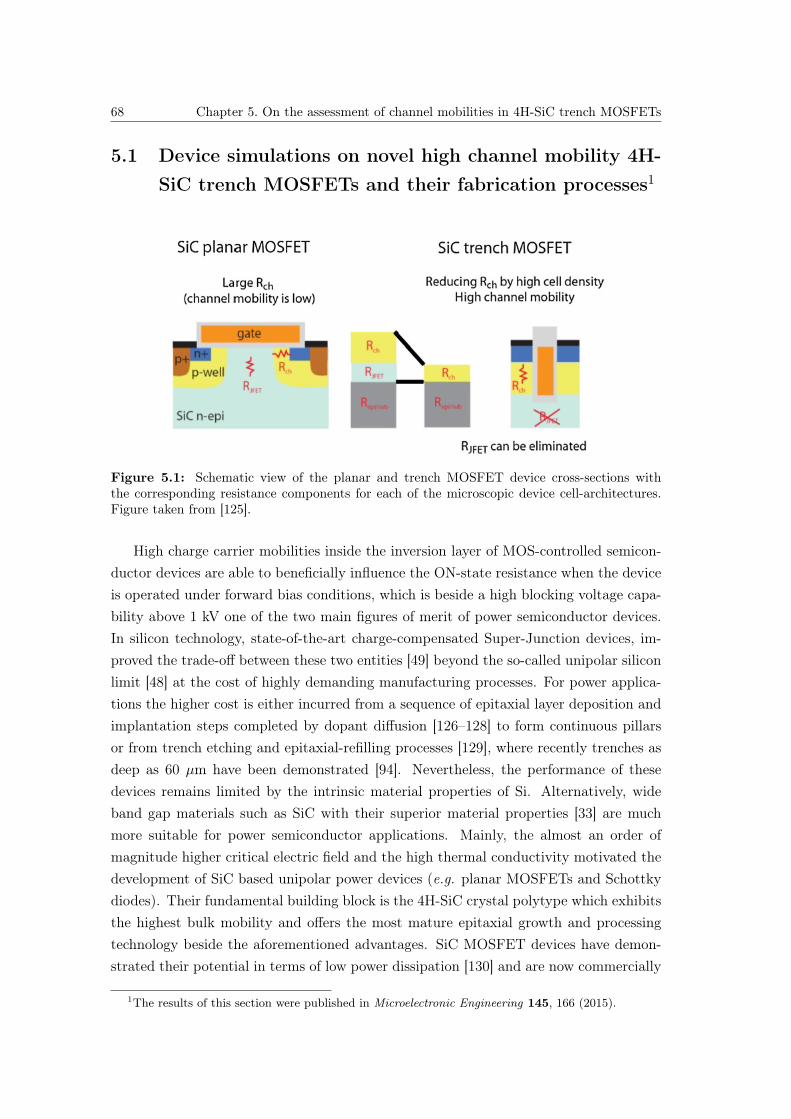
68 Chapter 5. On the assessment of channel mobilities in 4H-SiC trench MOSFETs
5.1 Device simulations on novel high channel mobility 4H-SiC trench MOSFETs and their fabrication processes1
Figure 5.1: Schematic view of the planar and trench MOSFET device cross-sections withthe corresponding resistance components for each of the microscopic device cell-architectures.Figure taken from [125].
High charge carrier mobilities inside the inversion layer of MOS-controlled semicon-ductor devices are able to beneficially influence the ON-state resistance when the deviceis operated under forward bias conditions, which is beside a high blocking voltage capa-bility above 1 kV one of the two main figures of merit of power semiconductor devices.In silicon technology, state-of-the-art charge-compensated Super-Junction devices, im-proved the trade-off between these two entities [49] beyond the so-called unipolar siliconlimit [48] at the cost of highly demanding manufacturing processes. For power applica-tions the higher cost is either incurred from a sequence of epitaxial layer deposition andimplantation steps completed by dopant diffusion [126–128] to form continuous pillarsor from trench etching and epitaxial-refilling processes [129], where recently trenches asdeep as 60 µm have been demonstrated [94]. Nevertheless, the performance of thesedevices remains limited by the intrinsic material properties of Si. Alternatively, wideband gap materials such as SiC with their superior material properties [33] are muchmore suitable for power semiconductor applications. Mainly, the almost an order ofmagnitude higher critical electric field and the high thermal conductivity motivated thedevelopment of SiC based unipolar power devices (e.g. planar MOSFETs and Schottkydiodes). Their fundamental building block is the 4H-SiC crystal polytype which exhibitsthe highest bulk mobility and offers the most mature epitaxial growth and processingtechnology beside the aforementioned advantages. SiC MOSFET devices have demon-strated their potential in terms of low power dissipation [130] and are now commercially
1The results of this section were published in Microelectronic Engineering 145, 166 (2015).
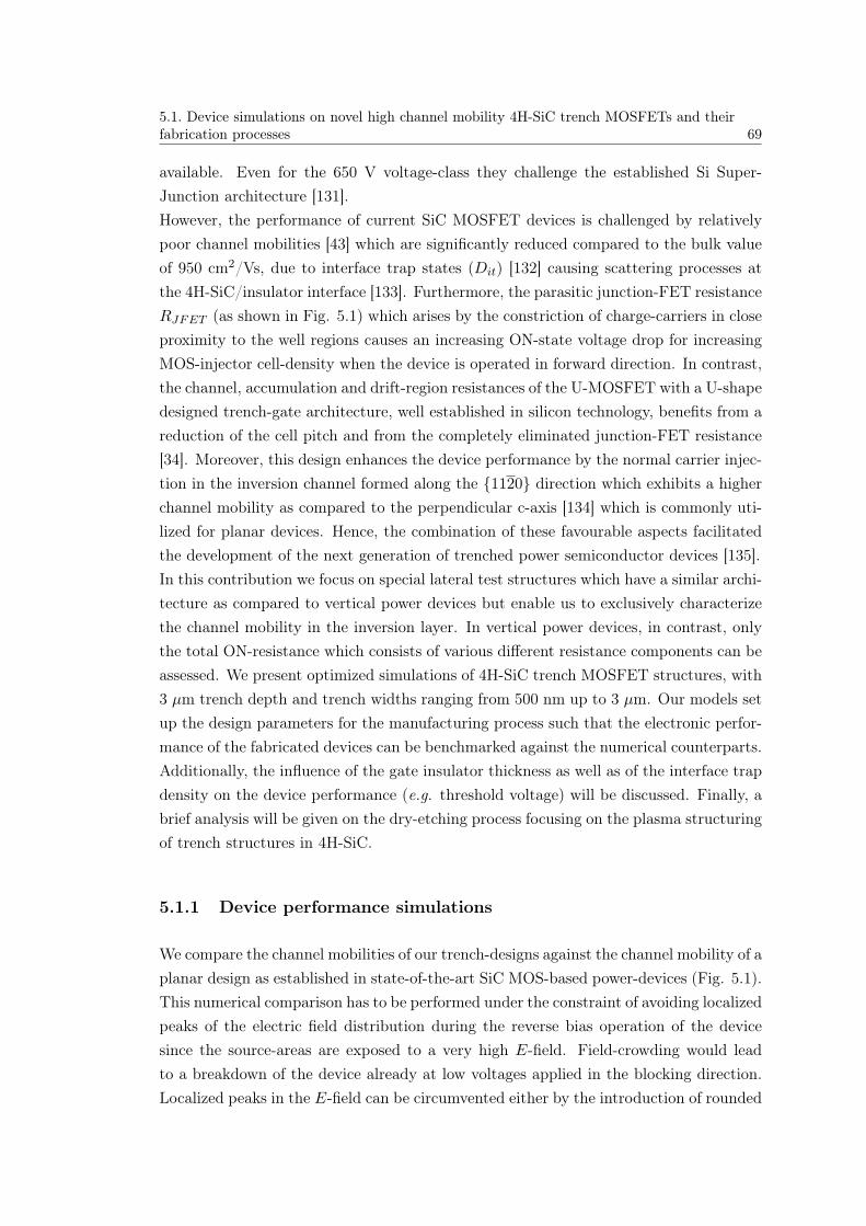
5.1. Device simulations on novel high channel mobility 4H-SiC trench MOSFETs and theirfabrication processes 69
available. Even for the 650 V voltage-class they challenge the established Si Super-Junction architecture [131].However, the performance of current SiC MOSFET devices is challenged by relativelypoor channel mobilities [43] which are significantly reduced compared to the bulk valueof 950 cm2/Vs, due to interface trap states (Dit) [132] causing scattering processes atthe 4H-SiC/insulator interface [133]. Furthermore, the parasitic junction-FET resistanceRJFET (as shown in Fig. 5.1) which arises by the constriction of charge-carriers in closeproximity to the well regions causes an increasing ON-state voltage drop for increasingMOS-injector cell-density when the device is operated in forward direction. In contrast,the channel, accumulation and drift-region resistances of the U-MOSFET with a U-shapedesigned trench-gate architecture, well established in silicon technology, benefits from areduction of the cell pitch and from the completely eliminated junction-FET resistance[34]. Moreover, this design enhances the device performance by the normal carrier injec-tion in the inversion channel formed along the 1120 direction which exhibits a higherchannel mobility as compared to the perpendicular c-axis [134] which is commonly uti-lized for planar devices. Hence, the combination of these favourable aspects facilitatedthe development of the next generation of trenched power semiconductor devices [135].In this contribution we focus on special lateral test structures which have a similar archi-tecture as compared to vertical power devices but enable us to exclusively characterizethe channel mobility in the inversion layer. In vertical power devices, in contrast, onlythe total ON-resistance which consists of various different resistance components can beassessed. We present optimized simulations of 4H-SiC trench MOSFET structures, with3 µm trench depth and trench widths ranging from 500 nm up to 3 µm. Our models setup the design parameters for the manufacturing process such that the electronic perfor-mance of the fabricated devices can be benchmarked against the numerical counterparts.Additionally, the influence of the gate insulator thickness as well as of the interface trapdensity on the device performance (e.g. threshold voltage) will be discussed. Finally, abrief analysis will be given on the dry-etching process focusing on the plasma structuringof trench structures in 4H-SiC.
5.1.1 Device performance simulations
We compare the channel mobilities of our trench-designs against the channel mobility of aplanar design as established in state-of-the-art SiC MOS-based power-devices (Fig. 5.1).This numerical comparison has to be performed under the constraint of avoiding localizedpeaks of the electric field distribution during the reverse bias operation of the devicesince the source-areas are exposed to a very high E-field. Field-crowding would leadto a breakdown of the device already at low voltages applied in the blocking direction.Localized peaks in the E-field can be circumvented either by the introduction of rounded
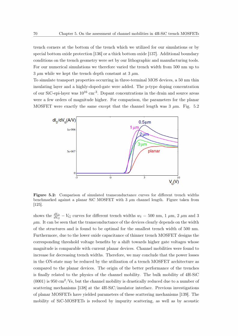
70 Chapter 5. On the assessment of channel mobilities in 4H-SiC trench MOSFETs
trench corners at the bottom of the trench which we utilized for our simulations or byspecial bottom oxide protection [136] or a thick bottom oxide [137]. Additional boundaryconditions on the trench geometry were set by our lithographic and manufacturing tools.For our numerical simulations we therefore varied the trench width from 500 nm up to3 µm while we kept the trench depth constant at 3 µm.To simulate transport properties occurring in three-terminal MOS devices, a 50 nm thininsulating layer and a highly-doped-gate were added. The p-type doping concentrationof our SiC-epi-layer was 1016 cm-3. Dopant concentrations in the drain and source areaswere a few orders of magnitude higher. For comparison, the parameters for the planarMOSFET were exactly the same except that the channel length was 3 µm. Fig. 5.2
Figure 5.2: Comparison of simulated transconductance curves for different trench widthsbenchmarked against a planar SiC MOSFET with 3 µm channel length. Figure taken from[125].
shows the dIDdVG− VG curves for different trench widths wt = 500 nm, 1 µm, 2 µm and 3
µm. It can be seen that the transconductance of the devices clearly depends on the widthof the structures and is found to be optimal for the smallest trench width of 500 nm.Furthermore, due to the lower oxide capacitance of thinner trench MOSFET designs thecorresponding threshold voltage benefits by a shift towards higher gate voltages whosemagnitude is comparable with current planar devices. Channel mobilities were found toincrease for decreasing trench widths. Therefore, we may conclude that the power lossesin the ON-state may be reduced by the utilization of a trench MOSFET architecture ascompared to the planar devices. The origin of the better performance of the trenchesis finally related to the physics of the channel mobility. The bulk mobility of 4H-SiC(0001) is 950 cm2/Vs, but the channel mobility is drastically reduced due to a number ofscattering mechanisms [138] at the 4H-SiC/insulator interface. Previous investigationsof planar MOSFETs have yielded parameters of these scattering mechanisms [139]. Themobility of SiC-MOSFETs is reduced by impurity scattering, as well as by acoustic
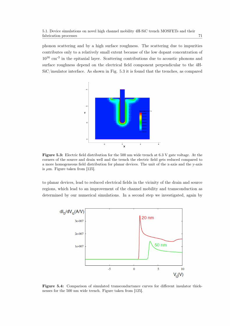
5.1. Device simulations on novel high channel mobility 4H-SiC trench MOSFETs and theirfabrication processes 71
phonon scattering and by a high surface roughness. The scattering due to impuritiescontributes only to a relatively small extent because of the low dopant concentration of1016 cm-3 in the epitaxial layer. Scattering contributions due to acoustic phonons andsurface roughness depend on the electrical field component perpendicular to the 4H-SiC/insulator interface. As shown in Fig. 5.3 it is found that the trenches, as compared
Figure 5.3: Electric field distribution for the 500 nm wide trench at 6.3 V gate voltage. At thecorners of the source and drain well and the trench the electric field gets reduced compared toa more homogeneous field distribution for planar devices. The unit of the x-axis and the y-axisis µm. Figure taken from [125].
to planar devices, lead to reduced electrical fields in the vicinity of the drain and sourceregions, which lead to an improvement of the channel mobility and transconduction asdetermined by our numerical simulations. In a second step we investigated, again by
Figure 5.4: Comparison of simulated transconductance curves for different insulator thick-nesses for the 500 nm wide trench. Figure taken from [125].

72 Chapter 5. On the assessment of channel mobilities in 4H-SiC trench MOSFETs
means of numerical simulations, the influence of the thickness of the gate insulator whichwe primarily set to 50 nm. As shown in Fig. 5.4, a reduction in the insulator thicknessto 20 nm is decreasing the threshold voltage while at the same time the channel-mobilitystays almost constant. The higher maximum value of the transconductance curve forthe smaller insulator thickness suggests lower switching losses but could also lead to apremature breakdown of the device.
5.1.2 Dry-etching of trenched MOS-controlled FETs
For inductively-coupled plasma (ICP) etching of targeted 3 µm deep trenches in 4H-SiCspecial test structures for chip sizes of 10 mm × 11 mm have been designed and producedby electron-beam lithography. As a hard mask material Chromium (Cr) has been chosensince it can be easily deposited by electron-beam evaporation and since it offers a highenough selectivity to etch 3 µm deep trenches for our process. The fabrication consistedof the following process sequence: Electron-beam evaporation of 100 nm of Cr, spincoating of 270 nm PMMA (950 k 4%) on top of the hard mask, electron-beam writing ofthe trench test structures into the PMMA layer, PMMA development, selective openingof the Cr hard mask by a reactive ion-etching (RIE) process using a plasma consisting ofa Cl2/O2 gas mixture. As a starting point for the ICP dry-etching process a SF6-based
Figure 5.5: Cross section of the etched trench profile of the 0.5 µm wide trench as imaged bySEM. Figure taken from [125].
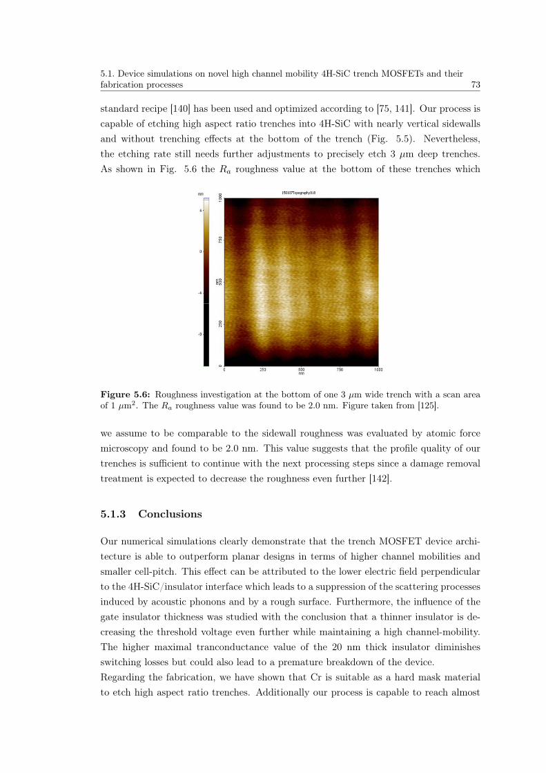
5.1. Device simulations on novel high channel mobility 4H-SiC trench MOSFETs and theirfabrication processes 73
standard recipe [140] has been used and optimized according to [75, 141]. Our process iscapable of etching high aspect ratio trenches into 4H-SiC with nearly vertical sidewallsand without trenching effects at the bottom of the trench (Fig. 5.5). Nevertheless,the etching rate still needs further adjustments to precisely etch 3 µm deep trenches.As shown in Fig. 5.6 the Ra roughness value at the bottom of these trenches which
Figure 5.6: Roughness investigation at the bottom of one 3 µm wide trench with a scan areaof 1 µm2. The Ra roughness value was found to be 2.0 nm. Figure taken from [125].
we assume to be comparable to the sidewall roughness was evaluated by atomic forcemicroscopy and found to be 2.0 nm. This value suggests that the profile quality of ourtrenches is sufficient to continue with the next processing steps since a damage removaltreatment is expected to decrease the roughness even further [142].
5.1.3 Conclusions
Our numerical simulations clearly demonstrate that the trench MOSFET device archi-tecture is able to outperform planar designs in terms of higher channel mobilities andsmaller cell-pitch. This effect can be attributed to the lower electric field perpendicularto the 4H-SiC/insulator interface which leads to a suppression of the scattering processesinduced by acoustic phonons and by a rough surface. Furthermore, the influence of thegate insulator thickness was studied with the conclusion that a thinner insulator is de-creasing the threshold voltage even further while maintaining a high channel-mobility.The higher maximal tranconductance value of the 20 nm thick insulator diminishesswitching losses but could also lead to a premature breakdown of the device.Regarding the fabrication, we have shown that Cr is suitable as a hard mask materialto etch high aspect ratio trenches. Additionally our process is capable to reach almost

74 Chapter 5. On the assessment of channel mobilities in 4H-SiC trench MOSFETs
perfect vertical sidewalls which support high mobilities. Furthermore, trenching effectsat the bottom of the trench could be eliminated by the optimization of the plasma dis-charge conditions. Nevertheless, further experiments to precisely determine the etchingrate still have to be performed.

CHAPTER 6
Summary and outlook
This thesis provides a detailed description of two fundamental aspects of semiconductortechnology, namely the characterization of electronically active dopant profiles whichdetermine the final device performance and the fabrication of power MOSFETs in SiC,whose wide band gap is offering superior power handling capabilities as compared to Si.Since the basic process flow of state of the art semiconductor devices requires variousprocessing steps until the final device is manufactured powerful metrology tools areurgently needed to monitor the dopant architecture after each step and to ensure thedesired device functionality at the end of the whole manufacturing cycle. Therefore itcan be understood that these two topics are strongly correlated even though the twoprojects have been independently initiated in the beginning.Within the following paragraphs a review on the past four years of my PhD work thatwas conducted at the Paul Scherrer Institute within the Laboratory for Micro- andNanotechnology will be given. Therefore the initial goals of each project project, theachievements and the importance of these results for the corresponding community willbe summarized.In the second part the work that is still ongoing as well as possible continuation strategieswill be discussed by the means of the acquired knowledge within this work and of thewhole research area.
75
76 Chapter 6. Summary and outlook
6.1 Achievements
The goal of the first project that is within the scope of this thesis was to address thecapabilities of SPM-based microscopy methods in terms of the quantification of electron-ically active dopant profiles. At the initial stage the scientific community recognized theimportance of characterization tools with a high spatial resolution that are able to quan-titatively assess informations on carrier and dopant profiles. The driving force behindthis development however was given by the ongoing miniaturization of devices. Herethe main focus was different since two dimensional electrical characterization tools wereneeded especially in areas where the assessment by C-V measurements of entire layerswas not sufficient anymore and on the other hand the sensitivity of carrier profilingmethods to the low dopant regime was investigated. The latter is of utmost importantfor lightly doped drift layers in power devices that are needed to sustain high reversevoltages without a premature breakdown of the device. For the assessment of the sen-sitivity of SPM-based methods special Si test structures were beforehand manufacturedin a similar way as Si Super-junction MOSFETs. Instead of the different terminals thatare present at the wafer surface in a real MOSFET these test structures have been com-plemented by calibration layers that were well-characterized by C-V measurements andlater on used to gauge the acquired SPM signals.From a material perspective Si was chosen to start with since it is still the most widelyused substrate even for power applications. The extension towards wide band gap ma-terials however was planned from the beginning. Among other things this was one ofthe main reasons to develop a polishing procedure since SiC can not be cleaved in avery controllable manner. Further a waste of the at this time costlier material shouldbe prevented. The focus on lightly doped layers was also driven by SiC since the in-trinsic carrier concentration is much lower than in Si and therefore a higher sensitivityfor this material is needed. Last but not least an explanation why the focus in thiswork is given to carrier and not dopant profiling techniques can be found by lookingat the different ionization energies of donor/acceptor atoms in SiC. Holes are tightlybound and therefore not all acceptors are ionized after the activation annealing. Thediscrepancy between the carrier and the dopant profile in this case can be sufficient tocause a malfunctioning of the device.As mentioned above one of the first achievements was the establishment of a reproduciblecross-section preparation routine that ensures a low surface state density and thereforeenables KPFM measurements. If this would not be the case the Fermi level would bepinned to defect states and the quantification possibilities of this method would com-pletely vanish. On this basis the comparison of three different SPM based methods,namely KPFM, SCFM and SSRM has been performed within the same custom builtAFM equipment. This has been a clear advancement as compared to previous studies
6.1. Achievements 77
since so far different methods were compared between different laboratories and also onthe basis of different calibration samples. Further the same parameters of the samplepreparation routine could not be guaranteed. Within the here presented analysis it wasfound that different information depths can be mapped depending on the underlyingphysical contrast mechanism of each method. Based on this investigation it can be con-cluded that the only reliable quantitative results can be gained by SSRM measurementssince for KPFM the high surface sensitivity of this method is prone to surface depletioneffects. SCFM on the other hand shows a high sensitivity for lightly doped layers andthe extended depletion capacitance is averaging out surface effects. The shape of thecorresponding spectroscopy curves however is not yet well understood. The often men-tioned disadvantage of SSRM, namely the destructive operation in contact mode, wasactually found to be key for a reliable quantification procedure due to the additionalself-preparation of the surface during the measurement. Notably, also the non-contactmeasurements were performed on the cross-section of a dedicated specimen which re-quires a ’destruction’ of the device.These findings were a high enough motivation to study the potential of SSRM in moredetail. Three possible methods for quantifying the carrier concentration inside the p-pillars of Super-junctions have been identified and discussed within this work. Onemethod is based on the variation of the width of the SCR under forward and reversebiasing the tip-sample junction. An other approach that has not been addressed so farwas the consideration of a dopant and temperature dependent mobility model for fittingthe experimental data of the calibration layers. Especially for dopant concentrationsaround NA,D = 1017 cm-3 the mobility is far away from being constant and insteadshows large variations with an increase or decrease of the concentration. Further, thenature of the tip-sample contact has been studied by I-V measurements. A Schottkycontact behaviour was observed and a clear differentiation of the resulting I-V curvesfor each concentration was possible. These data sets were fitted by an extended ther-moionic emission model which takes also a shunt resistance into account. The extractedfit parameters were showing reasonable trends however the quantification potential bythe dopant dependent barrier lowering contribution still needs further investigation.Simultaneously to the above described developments these concepts have been extendedto SiC where two technologically relevant problems have been analysed. One of them isthe characterization of epitaxially grown n-type 4H-SiC layers while the other one is theimaging of a p-doped shielding structure of a Schottky barrier diode. It was found thatresolution at the boundaries between differently doped n-type regions is blurred out dueto the presence of surface defects that cause band bending effects. The application ofa surface photo voltage which gets established under laser illumination of the samplewas able to diminish this effect. This is due to the fact electron-hole pairs are generatedwithin the semiconductor that can diffuse towards the surface and passivate those defect

78 Chapter 6. Summary and outlook
states. Hence this analysis method is a suitable tool to characterize the sharpness of thejunction between differently doped epitaxial layers. For the shielding structures presentbelow the Schottky contact the EFM based methods revealed more details as comparedto SEPC measurements.The second project that is covered within the scope of this thesis was related to thefabrication of lateral trench MOSFETs in 4H-SiC. Notably, the structure is very similarto vertical power devices that have been already fabricated and characterized. The nov-elty of the here presented structure lies in the fact that the channel resistance can beprecisely addressed. Especially in the medium power range the ON-state resistance con-tribution of the channel is quite significant while in the high power regime the resistancecontribution of the drift region is dominant. In the initial stage of this project focuswas given to device simulations to determine the optimal trench geometry in terms ofa high channel mobility. In parallel ICP etch tests on small chips have been performedto determine the optimal etching parameters for the desired trench structures. This hasbeen done in an iterative trial and error manner that was backed up by the few availableliterature reports. After the optimization of this challenging process the whole processflow with the corresponding mask layouts has been designed. Based on this design theion implantation step was carried out by a subcontractor and in parallel first MOS Ca-pacitors have been fabricated. The challenging oxidation step as well as the necessity ofadditional outsourced processes however lead to the fact that work towards a full trenchMOSFET is still ongoing.
6.2. Ongoing and future work 79
6.2 Ongoing and future work
Regarding the dopant imaging project further investigations on the SSRM quantificationprocedure are still ongoing. Most recent results according to the I-V measurements haveshown a Schottky contact behaviour. In contrast the fit of the experimental data thatis based on the Arora mobility model was taking only an ohmic contact into account.Therefore this model needs to be extended accordingly. Further, due to the low dopantconcentration inside the trench new calibration structures have to be fabricated wherethe lowest doping level of one of the calibration layers has to be below the doping con-centration inside the trench.Once these challenges are overcome one can think of the visualization of dopant profilesand the corresponding space charge regions during the operation of the device as it hasbeen done for SCM measurements [143]. These kind of measurements on one hand wouldneed a proper contact patterning of the backside contact and of the contacts where thevoltage is applied to the device. On the other hand a modification of the AFM system isrequired. Problems regarding the ageing of devices could in this way be systematicallystudied. From this possibility the device failure analysis would benefit since to the bestof my knowledge this is nowadays only done after the device is fully broken after numer-ous load and unload cycles. However it is speculated that modifications of the dopantprofile occur beforehand. Therefore new insights in terms of a reliable device design canbe gathered.Regarding the second project preliminary results suggested that the thermal oxidegrowth on 4H-SiC is limited due to the maximum operating temperature of our oxi-dation furnace of 1050 C. Due to the presence of C atoms the oxidation process isshowing a higher complexity and the subsequent passivation mechanisms to neutralizethe effect of interface trap states are not yet well understood. In the case of trenchdevices it also has to be considered that a thermally grown oxide is anisotropic. For aSi-face substrate as it was used here this would result in a higher oxide thickness at thetrench sidewalls as compared to the trench bottom. The highest electric fields when thedevice is operated in reverse direction however is expected to built up at the horizontalinterface at the trench bottom. Therefore in our configuration this anisotropy wouldresult in a lower voltage class of the device. Hence, high k-materials with a larger di-electric constant that can be conformally deposited by Atomic Layer Deposition (ALD)are promising candidates as gate insulators. Furthermore, high-k gate dielectrics inducea lower electric field inside the thin conducting channel that is formed when the gatevoltage exceeds the threshold voltage. This allows fore a more reliable gate operationat lower gate voltages since the threshold voltage is shifted to lower values due to thehigher gate capacitance as compared to SiO2. The unfavourable effect of a high dielectricconstant on the mobility gets compensated by a higher transconductance. Potential im-

80 Chapter 6. Summary and outlook
provements have already been demonstrated in planar devices [144, 145] and the logicalnext step is to use this technology also for trench MOSFETs. The addition of a nitrogenconditioning step [146] before the ALD deposition of the gate insulator is expected toproduce a high quality surface in terms of a low roughness and a low density of interfacestates. Hence the combination of these two concepts might enable a new class of highenergy efficient power MOSFETs.

Bibliography
[1] T. Jenkins. A brief history of ... semiconductors. Physics Education, 40(5):430,2005.
[2] L. Łukasiak and A. Jakubowski. History of semiconductors. Journal of Telecom-munications and information technology, pages 3–9, 2010.
[3] G. Busch. Early history of the physics and chemistry of semiconductors-fromdoubts to fact in a hundred years. European Journal of Physics, 10(4):254, 1989.
[4] A. Volta and Hon. G. E. Cowper. Del Modo di Render Sensibilissima la piuDebole Elettricita sia Naturale, sia Artificiale. By Mr. Alexander Volta, Professorof Experimental Philosophy in Como, &c. &c.; Communicated by the Right Hon.George Earl Cowper, F. R. S. Philosophical Transactions of the Royal Society ofLondon, 72:237–xxxiii, 1782.
[5] M. Faraday. Experimental Researches in Electricity. Fourth Series. PhilosophicalTransactions of the Royal Society of London, 123:507–522, 1833.
[6] H. Davy. Farther Researches on the Magnetic Phaenomena Produced by Electric-ity; With Some New Experiments on the Properties of Electrified Bodies in TheirRelations to Conducting Powers and Temperature. Philosophical Transactions ofthe Royal Society of London, 111:425–439, 1821.
[7] E. Riecke. Zur Theorie des Galvanismus und der Wärme. Annalen der Physik,302(11):353–581, 1898.
[8] J. J. Thomson. XL. Cathode Rays . Philosophical Magazine Series 5, 44(269):293–316, 1897.
81
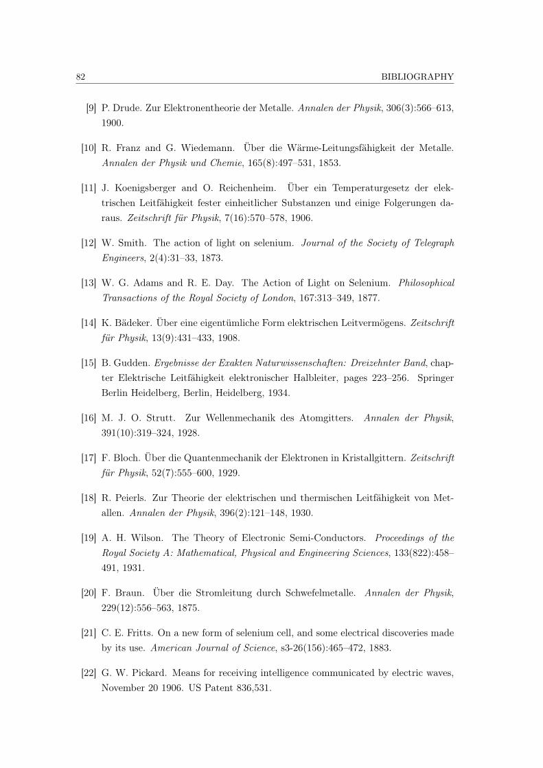
82 BIBLIOGRAPHY
[9] P. Drude. Zur Elektronentheorie der Metalle. Annalen der Physik, 306(3):566–613,1900.
[10] R. Franz and G. Wiedemann. Über die Wärme-Leitungsfähigkeit der Metalle.Annalen der Physik und Chemie, 165(8):497–531, 1853.
[11] J. Koenigsberger and O. Reichenheim. Über ein Temperaturgesetz der elek-trischen Leitfähigkeit fester einheitlicher Substanzen und einige Folgerungen da-raus. Zeitschrift für Physik, 7(16):570–578, 1906.
[12] W. Smith. The action of light on selenium. Journal of the Society of TelegraphEngineers, 2(4):31–33, 1873.
[13] W. G. Adams and R. E. Day. The Action of Light on Selenium. PhilosophicalTransactions of the Royal Society of London, 167:313–349, 1877.
[14] K. Bädeker. Über eine eigentümliche Form elektrischen Leitvermögens. Zeitschriftfür Physik, 13(9):431–433, 1908.
[15] B. Gudden. Ergebnisse der Exakten Naturwissenschaften: Dreizehnter Band, chap-ter Elektrische Leitfähigkeit elektronischer Halbleiter, pages 223–256. SpringerBerlin Heidelberg, Berlin, Heidelberg, 1934.
[16] M. J. O. Strutt. Zur Wellenmechanik des Atomgitters. Annalen der Physik,391(10):319–324, 1928.
[17] F. Bloch. Über die Quantenmechanik der Elektronen in Kristallgittern. Zeitschriftfür Physik, 52(7):555–600, 1929.
[18] R. Peierls. Zur Theorie der elektrischen und thermischen Leitfähigkeit von Met-allen. Annalen der Physik, 396(2):121–148, 1930.
[19] A. H. Wilson. The Theory of Electronic Semi-Conductors. Proceedings of theRoyal Society A: Mathematical, Physical and Engineering Sciences, 133(822):458–491, 1931.
[20] F. Braun. Über die Stromleitung durch Schwefelmetalle. Annalen der Physik,229(12):556–563, 1875.
[21] C. E. Fritts. On a new form of selenium cell, and some electrical discoveries madeby its use. American Journal of Science, s3-26(156):465–472, 1883.
[22] G. W. Pickard. Means for receiving intelligence communicated by electric waves,November 20 1906. US Patent 836,531.
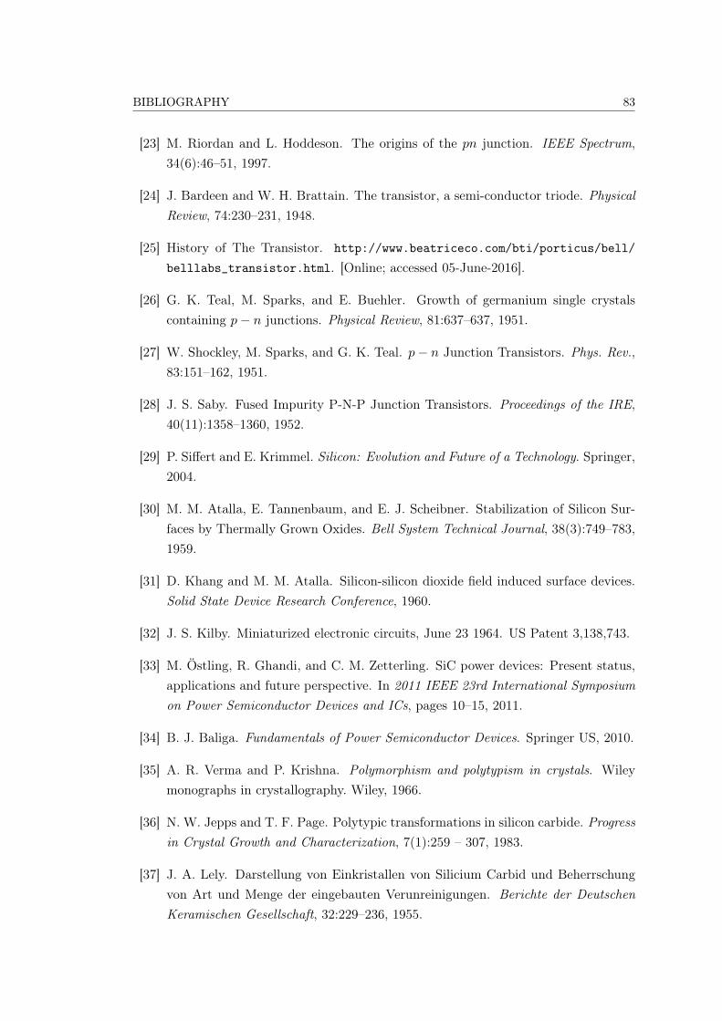
BIBLIOGRAPHY 83
[23] M. Riordan and L. Hoddeson. The origins of the pn junction. IEEE Spectrum,34(6):46–51, 1997.
[24] J. Bardeen and W. H. Brattain. The transistor, a semi-conductor triode. PhysicalReview, 74:230–231, 1948.
[25] History of The Transistor. http://www.beatriceco.com/bti/porticus/bell/
belllabs_transistor.html. [Online; accessed 05-June-2016].
[26] G. K. Teal, M. Sparks, and E. Buehler. Growth of germanium single crystalscontaining p− n junctions. Physical Review, 81:637–637, 1951.
[27] W. Shockley, M. Sparks, and G. K. Teal. p− n Junction Transistors. Phys. Rev.,83:151–162, 1951.
[28] J. S. Saby. Fused Impurity P-N-P Junction Transistors. Proceedings of the IRE,40(11):1358–1360, 1952.
[29] P. Siffert and E. Krimmel. Silicon: Evolution and Future of a Technology. Springer,2004.
[30] M. M. Atalla, E. Tannenbaum, and E. J. Scheibner. Stabilization of Silicon Sur-faces by Thermally Grown Oxides. Bell System Technical Journal, 38(3):749–783,1959.
[31] D. Khang and M. M. Atalla. Silicon-silicon dioxide field induced surface devices.Solid State Device Research Conference, 1960.
[32] J. S. Kilby. Miniaturized electronic circuits, June 23 1964. US Patent 3,138,743.
[33] M. Östling, R. Ghandi, and C. M. Zetterling. SiC power devices: Present status,applications and future perspective. In 2011 IEEE 23rd International Symposiumon Power Semiconductor Devices and ICs, pages 10–15, 2011.
[34] B. J. Baliga. Fundamentals of Power Semiconductor Devices. Springer US, 2010.
[35] A. R. Verma and P. Krishna. Polymorphism and polytypism in crystals. Wileymonographs in crystallography. Wiley, 1966.
[36] N. W. Jepps and T. F. Page. Polytypic transformations in silicon carbide. Progressin Crystal Growth and Characterization, 7(1):259 – 307, 1983.
[37] J. A. Lely. Darstellung von Einkristallen von Silicium Carbid und Beherrschungvon Art und Menge der eingebauten Verunreinigungen. Berichte der DeutschenKeramischen Gesellschaft, 32:229–236, 1955.
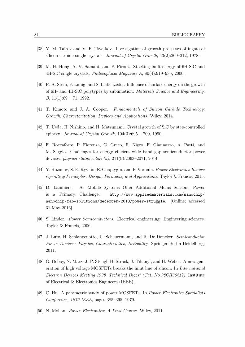
84 BIBLIOGRAPHY
[38] Y. M. Tairov and V. F. Tsvetkov. Investigation of growth processes of ingots ofsilicon carbide single crystals. Journal of Crystal Growth, 43(2):209–212, 1978.
[39] M. H. Hong, A. V. Samant, and P. Pirouz. Stacking fault energy of 6H-SiC and4H-SiC single crystals. Philosophical Magazine A, 80(4):919–935, 2000.
[40] R. A. Stein, P. Lanig, and S. Leibenzeder. Influence of surface energy on the growthof 6H- and 4H-SiC polytypes by sublimation. Materials Science and Engineering:B, 11(1):69 – 71, 1992.
[41] T. Kimoto and J. A. Cooper. Fundamentals of Silicon Carbide Technology:Growth, Characterization, Devices and Applications. Wiley, 2014.
[42] T. Ueda, H. Nishino, and H. Matsunami. Crystal growth of SiC by step-controlledepitaxy. Journal of Crystal Growth, 104(3):695 – 700, 1990.
[43] F. Roccaforte, P. Fiorenza, G. Greco, R. Nigro, F. Giannazzo, A. Patti, andM. Saggio. Challenges for energy efficient wide band gap semiconductor powerdevices. physica status solidi (a), 211(9):2063–2071, 2014.
[44] Y. Rozanov, S. E. Ryvkin, E. Chaplygin, and P. Voronin. Power Electronics Basics:Operating Principles, Design, Formulas, and Applications. Taylor & Francis, 2015.
[45] D. Lammers. As Mobile Systems Offer Additional Mems Sensors, Poweris a Primary Challenge. http://www.appliedmaterials.com/nanochip/
nanochip-fab-solutions/december-2013/power-struggle. [Online; accessed31-May-2016].
[46] S. Linder. Power Semiconductors. Electrical engineering: Engineering sciences.Taylor & Francis, 2006.
[47] J. Lutz, H. Schlangenotto, U. Scheuermann, and R. De Doncker. SemiconductorPower Devices: Physics, Characteristics, Reliability. Springer Berlin Heidelberg,2011.
[48] G. Deboy, N. Marz, J.-P. Stengl, H. Strack, J. Tihanyi, and H. Weber. A new gen-eration of high voltage MOSFETs breaks the limit line of silicon. In InternationalElectron Devices Meeting 1998. Technical Digest (Cat. No.98CH36217). Instituteof Electrical & Electronics Engineers (IEEE).
[49] C. Hu. A parametric study of power MOSFETs. In Power Electronics SpecialistsConference, 1979 IEEE, pages 385–395, 1979.
[50] N. Mohan. Power Electronics: A First Course. Wiley, 2011.
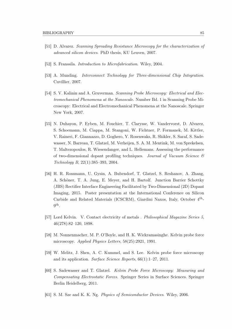
BIBLIOGRAPHY 85
[51] D. Alvarez. Scanning Spreading Resistance Microscopy for the characterization ofadvanced silicon devices. PhD thesis, KU Leuven, 2007.
[52] S. Franssila. Introduction to Microfabrication. Wiley, 2004.
[53] A. Munding. Interconnect Technology for Three-dimensional Chip Integration.Cuvillier, 2007.
[54] S. V. Kalinin and A. Gruverman. Scanning Probe Microscopy: Electrical and Elec-tromechanical Phenomena at the Nanoscale. Number Bd. 1 in Scanning Probe Mi-croscopy: Electrical and Electromechanical Phenomena at the Nanoscale. SpringerNew York, 2007.
[55] N. Duhayon, P. Eyben, M. Fouchier, T. Clarysse, W. Vandervorst, D. Alvarez,S. Schoemann, M. Ciappa, M. Stangoni, W. Fichtner, P. Formanek, M. Kittler,V. Raineri, F. Giannazzo, D. Goghero, Y. Rosenwaks, R. Shikler, S. Saraf, S. Sade-wasser, N. Barreau, T. Glatzel, M. Verheijen, S. A. M. Mentink, M. von Sprekelsen,T. Maltezopoulos, R. Wiesendanger, and L. Hellemans. Assessing the performanceof two-dimensional dopant profiling techniques. Journal of Vacuum Science &Technology B, 22(1):385–393, 2004.
[56] H. R. Rossmann, U. Gysin, A. Bubendorf, T. Glatzel, S. Reshanov, A. Zhang,A. Schöner, T. A. Jung, E. Meyer, and H. Bartolf. Junction Barrier Schottky(JBS) Rectifier Interface Engineering Facilitated by Two-Dimensional (2D) DopantImaging, 2015. Poster presentation at the International Conference on SiliconCarbide and Related Materials (ICSCRM), Giardini Naxos, Italy, October 4th-9th.
[57] Lord Kelvin. V. Contact electricity of metals . Philosophical Magazine Series 5,46(278):82–120, 1898.
[58] M. Nonnenmacher, M. P. O’Boyle, and H. K. Wickramasinghe. Kelvin probe forcemicroscopy. Applied Physics Letters, 58(25):2921, 1991.
[59] W. Melitz, J. Shen, A. C. Kummel, and S. Lee. Kelvin probe force microscopyand its application. Surface Science Reports, 66(1):1–27, 2011.
[60] S. Sadewasser and T. Glatzel. Kelvin Probe Force Microscopy: Measuring andCompensating Electrostatic Forces. Springer Series in Surface Sciences. SpringerBerlin Heidelberg, 2011.
[61] S. M. Sze and K. K. Ng. Physics of Semiconductor Devices. Wiley, 2006.
86 BIBLIOGRAPHY
[62] K. Kobayashi, H. Yamada, and K. Matsushige. Dopant profiling on semiconductingsample by scanning capacitance force microscopy. Applied Physics Letters, 81(14),2002.
[63] A. Kikukawa, S. Hosaka, and R. Imura. Vacuum compatible high-sensitive Kelvinprobe force microscopy. Review of Scientific Instruments, 67(4), 1996.
[64] U. Gysin, E. Meyer, Th. Glatzel, G. Günzburger, H. R. Rossmann, T. A. Jung,S. Reshanov, A. Schöner, and H. Bartolf. Dopant imaging of power semiconductordevice cross sections. Microelectronic Engineering, 160:18 – 21, 2016.
[65] P. De Wolf, J. Snauwaert, T. Clarysse, W. Vandervorst, and L. Hellemans. Charac-terization of a point-contact on silicon using force microscopy-supported resistancemeasurements. Applied Physics Letters, 66(12):1530–1532, 1995.
[66] T. Clarysse, D. Vanhaeren, I. Hoflijk, and W. Vandervorst. Characterization ofelectrically active dopant profiles with the spreading resistance probe. MaterialsScience and Engineering: R: Reports, 47(5):123–206, 2004.
[67] P. Eyben. Scanning spreading resistance microscopy: High resolution two-dimensional carrier profiling of semiconductor structures. PhD thesis, KU Leuven,2004.
[68] R. Holm and E. Holm. Electric contacts: theory and application. Springer-Verlag,1967.
[69] T. Clarysse, M. Caymax, P. De Wolf, T. Trenkler, W. Vandervorst, J. S. McMur-ray, J. Kim, C. C. Williams, J. G. Clark, and G. Neubauer. Epitaxial staircasestructure for the calibration of electrical characterization techniques. Journal ofVacuum Science & Technology B, 16(1):394–400, 1998.
[70] P. Eyben, M. Xu, N. Duhayon, T. Clarysse, S. Callewaert, and W. Vandervorst.Scanning spreading resistance microscopy and spectroscopy for routine and quanti-tative two-dimensional carrier profiling. Journal of Vacuum Science & TechnologyB, 20(1), 2002.
[71] H.R. Rossmann, A. Bubendorf, F. Zanella, N. Marjanovic, M. Schnieper, E. Meyer,T.A. Jung, J. Gobrecht, R.A. Minamisawa, and H. Bartolf. Physical Studies of SiCNano-Trench-MOSFETs, 2015. Prolongation proposal for the NanoSiCTrenchFETproject.
[72] A. Baudrant. Silicon Technologies: Ion Implantation and Thermal Treatment.ISTE. Wiley, 2013.
BIBLIOGRAPHY 87
[73] M. D. Henry. ICP etching of Silicon. PhD thesis, California Institute of Technology,2010.
[74] F. A. Khan and I. Adesida. High rate etching of SiC using inductively coupledplasma reactive ion etching in SF6-based gas mixtures. Applied Physics Letters,75(15), 1999.
[75] D. Alquier, E. Collard, J. F. Michaud, and J. Biscarrat. ICP Etching of 4H-SiCSubstrates. In Silicon Carbide and Related Materials 2012, volume 740 ofMaterialsScience Forum, pages 825–828. Trans Tech Publications, 2013.
[76] H. Ru, Y. Yin-Tang, and F. Xiao-Ya. Microtrenching geometry of 6H-SiC plasmaetching. Vacuum, 84(3):400 – 404, 2009.
[77] B. E. Deal and A. S. Grove. General Relationship for the Thermal Oxidation ofSilicon. Journal of Applied Physics, 36(12), 1965.
[78] Y. Song, S. Dhar, L. C. Feldman, G. Chung, and J. R. Williams. Modified DealGrove model for the thermal oxidation of silicon carbide. Journal of AppliedPhysics, 95(9), 2004.
[79] Y. Hijikata, H. Yaguchi, and S. Yoshida. A Kinetic Model of Silicon CarbideOxidation Based on the Interfacial Silicon and Carbon Emission Phenomenon.Applied Physics Express, 2(2):021203, 2009.
[80] V. V. Afanasev, M. Bassler, G. Pensl, and M. Schulz. Intrinsic SiC/SiO2 InterfaceStates. physica status solidi (a), 162(1):321–337, 1997.
[81] G. Liu, B. R. Tuttle, and S. Dhar. Silicon carbide: A unique platform for metal-oxide-semiconductor physics. Applied Physics Reviews, 2(2), 2015.
[82] Y. Nanen, M. Kato, J. Suda, and T. Kimoto. Effects of Nitridation on 4H-SiCMOSFETs Fabricated on Various Crystal Faces. IEEE Transactions on ElectronDevices, 60(3):1260–1262, 2013.
[83] S. Y. Han, K. H. Kim, J. K. Kim, H. W. Jang, K. H. Lee, N.-K. Kim, E. D. Kim,and J.-L. Lee. Ohmic contact formation mechanism of ni on n-type 4h-sic. AppliedPhysics Letters, 79(12):1816–1818, 2001.
[84] S. A. Reshanov, K. V. Emtsev, F. Speck, K.-Y. Gao, T. K. Seyller, G. Pensl, andL. Ley. Effect of an intermediate graphite layer on the electronic properties ofmetal/SiC contacts. physica status solidi (b), 245(7):1369–1377, 2008.
[85] D. K. Schroder. Semiconductor Material and Device Characterization. Wiley,2006.
88 BIBLIOGRAPHY
[86] R. Subrahmanyan. Methods for the measurement of two-dimensional doping pro-files. Journal of Vacuum Science & Technology B, 10(1):358–368, 1992.
[87] 3rd International Technology Roadmap for Semiconductors 2013 Edition.
[88] P. De Wolf, R. Stephenson, T. Trenkler, T. Clarysse, T. Hantschel, and W. Van-dervorst. Status and review of two-dimensional carrier and dopant profiling us-ing scanning probe microscopy. Journal of Vacuum Science & Technology B,18(1):361–368, 2000.
[89] P. C. Zalm. Ultra shallow doping profiling with SIMS. Reports on Progress inPhysics, 58(10):1321, 1995.
[90] Y. Martin, D. W. Abraham, and H. K. Wickramasinghe. High-resolution ca-pacitance measurement and potentiometry by force microscopy. Applied PhysicsLetters, 52(13):1103, 1988.
[91] E. Meyer, S. Reshanov, H. Bartolf, A. Schöner, U. Gysin, A. Bubendorf, T. Glatzel,H. R. Rossmann, and T. A. Jung. Two-Dimensional Carrier Profiling on LightlyDoped n-Type 4H-SiC Epitaxially Grown Layers. In Silicon Carbide and RelatedMaterials 2014, volume 821 of Materials Science Forum, pages 269–272. TransTech Publications, 2015.
[92] W. Saito. Theoretical limits of superjunction considering with charge imbalancemargin. In 2015 IEEE 27th International Symposium on Power SemiconductorDevices IC’s (ISPSD), pages 125–128, 2015.
[93] T. Fujihira. Theory of Semiconductor Superjunction Devices. Japanese Journalof Applied Physics, 36(Part 1, No. 10):6254–6262, 1997.
[94] H. Bartolf, A. Mihaila, I. Nistor, M. Jurisch, B. Leibold, and M. Zimmermann. De-velopment of a 60 µm Deep Trench and Refill Process for Manufacturing Si-BasedHigh-Voltage Super-Junction Structures. IEEE Transactions on SemiconductorManufacturing, 26(4):529–541, 2013.
[95] A. Kikukawa, S. Hosaka, and R. Imura. Vacuum compatible high-sensitive Kelvinprobe force microscopy. Review of Scientific Instruments, 67(4):1463–1467, 1996.
[96] J. R. Matey and J. Blanc. Scanning capacitance microscopy. Journal of AppliedPhysics, 57(5):1437–1444, 1985.
[97] U. Gysin, T. Glatzel, T. Schmölzer, A. Schöner, S. Reshanov, H. Bartolf, andE. Meyer. Large area scanning probe microscope in ultra-high vacuum demon-strated for electrostatic force measurements on high-voltage devices. BeilsteinJournal of Nanotechnology, 6:2485–2497, 2015.
BIBLIOGRAPHY 89
[98] L. Kronik. Surface photovoltage phenomena: theory, experiment, and applications.Surface Science Reports, 37(1-5):1–206, 1999.
[99] C. Sommerhalter, T. Glatzel, T. W. Matthes, A. Jäger-Waldau, and M. C. Lux-Steiner. Kelvin probe force microscopy in ultra high vacuum using amplitude mod-ulation detection of the electrostatic forces. Applied Surface Science, 157(4):263 –268, 2000.
[100] J. Mody, R. Duffy, P. Eyben, J. Goossens, A. Moussa, W. Polspoel, B. Berghmans,M. J. H. van Dal, B. J. Pawlak, M. Kaiser, R. G. R. Weemaes, and W. Vandervorst.Experimental studies of dose retention and activation in fin field-effect-transistor-based structures. Journal of Vacuum Science & Technology B, 28(1), 2010.
[101] P. Eyben, P. Bisiaux, A. Schulze, A. Nazir, and W. Vandervorst. Fast Fouriertransform scanning spreading resistance microscopy: a novel technique to over-come the limitations of classical conductive AFM techniques. Nanotechnology,26(35):355702, 2015.
[102] A. Schulze, R. Cao, P. Eyben, T. Hantschel, and W. Vandervorst. Outwittingthe series resistance in scanning spreading resistance microscopy. Ultramicroscopy,161:59–65, 2016.
[103] N. D. Arora, J. R. Hauser, and D. J. Roulston. Electron and hole mobilities insilicon as a function of concentration and temperature. IEEE Transactions onElectron Devices, 29(2):292–295, 1982.
[104] L. Zhang, M. Koike, M. Ono, S. Itai, K. Matsuzawa, S. Ono, W. Saito, M. Ya-maguchi, Y. Hayase, and K. Hara. Comprehensive 2d-carrier profiling of low-doping region by high-sensitivity scanning spreading resistance microscopy (ssrm)for power device applications. Microelectronics Reliability, 55(9-10):1559–1563,2015. Proceedings of the 26th European Symposium on Reliability of ElectronDevices 2015.
[105] D. Schröder. Leistungselektronische Bauelemente. Springer-Lehrbuch. SpringerBerlin Heidelberg, 2008.
[106] T. Hantschel, C. Demeulemeester, P. Eyben, V. Schulz, O. Richard, H. Bender, andW. Vandervorst. Conductive diamond tips with sub-nanometer electrical resolutionfor characterization of nanoelectronics device structures. physica status solidi (a),206(9):2077–2081, 2009.
[107] R. P. Lu, K. L. Kavanagh, S. J. Dixon-Warren, A. J. Spring-Thorpe, R. Streater,and I. Calder. Scanning spreading resistance microscopy current transport studies
90 BIBLIOGRAPHY
on doped III-V semiconductors. Journal of Vacuum Science & Technology B, 20(4),2002.
[108] P. Chattopadhyay. The effect of shunt resistance on the electrical characteristics ofSchottky barrier diodes. Journal of Physics D: Applied Physics, 29(3):823, 1996.
[109] R. J. Hillard, R. G. Mazur, H. L. Berkowitz, and P. Raj-Choudhury. Profiling ofsilicon and III-V compounds by point contact techniques. Solid State Technology,32(8):119–126, 1989.
[110] L. Hao and P. A. Bennett. Minority carrier effects in nanoscale Schottky contacts.Nanotechnology, 20(35):355201, 2009.
[111] L. Hao and P. A. Bennett. Analytic model for minority carrier effects in nanoscaleSchottky contacts. Journal of Applied Physics, 108(1), 2010.
[112] P. De Wolf, R. Stephenson, T. Trenkler, T. Clarysse, T. Hantschel, and W. Van-dervorst. Status and review of two-dimensional carrier and dopant profiling usingscanning probe microscopy. Journal of Vacuum Science & Technology B, 18(1):361,2000.
[113] A. Henning, G. Günzburger, R. Jöhr, Y. Rosenwaks, B. Bozic-Weber, C. E. House-croft, E. C. Constable, E. Meyer, and T. Glatzel. Kelvin probe force microscopyof nanocrystalline TiO2 photoelectrodes. Beilstein Journal of Nanotechnology,4:418–428, 2013.
[114] K. Asano, T. Hayashi, R. Saito, and Y. Sugawara. High temperature static anddynamic characteristics of 3.7 kV high voltage 4H-SiC JBS. In Power Semicon-ductor Devices and ICs, 2000. Proceedings. The 12th International Symposium on,pages 97–100, 2000.
[115] M. Kushibe, S. Imai, T. Shinohe, T. Hatakeyama, and T. Watanabe. OptimumDesign of a SiC Schottky Barrier Diode Considering Reverse Leakage Current dueto a Tunneling Process. In Silicon Carbide and Related Materials - 2002, volume433 of Materials Science Forum, pages 831–834. Trans Tech Publications, 2003.
[116] B. M. Wilamowski. Schottky diodes with high breakdown voltages. Solid-StateElectronics, 26(5):491 – 493, 1983.
[117] E. Meyer, H. Bartolf, A. Schöner, A. Zhang, U. Gysin, A. Bubendorf, T. Glatzel,S. A. Reshanov, H.R. Rossmann, and T.A. Jung. Junction Barrier Schottky (JBS)Rectifier Interface Engineering Facilitated by Two-Dimensional (2D) Dopant Imag-ing. In Silicon Carbide and Related Materials 2015, volume 858 of Materials Sci-ence Forum, pages 497–500. Trans Tech Publications, 2016.

BIBLIOGRAPHY 91
[118] H. Bartolf, V. K. Sundaramoohrty, and A. Mihaila. Simulation Study of aJBS-Rectifier with Close to Schottky-Interface Conduction Investigated for High-Voltage Classes. In Silicon Carbide and Related Materials - 2002, Proc. 12thInternational Seminar on Power Semiconductors, pages 85–90, 2014.
[119] M. Bakowski, J.-K. Lim, and W. Kaplan. Merits of Buried Grid Technology forSiC JBS Diodes. ECS Transactions, 50(3):415–424, 2013.
[120] H. Bartolf, A. Mihaila, L. Knoll, V. K. Sundaramoorthy, R. A. Minamisawa, andE. Bianda. JBS power-rectifiers for 1.7 kV applications with conduction propertiesclose to pure Schottky-design. In 2015 17th European Conference on Power Elec-tronics and Applications (EPE15 ECCE-Europe). Institute of Electrical & Elec-tronics Engineers (IEEE), 2015.
[121] H. Bartolf, U. Gysin, H. R. Rossmann, A. Bubendorf, T. Glatzel, T. A. Jung,E. Meyer, M. Zimmermann, S. Reshanov, and A. Schöner. Development of powersemiconductors by quantitative nanoscale dopant imaging. In 2015 IEEE 27th In-ternational Symposium on Power Semiconductor Devices & ICs (ISPSD). Instituteof Electrical & Electronics Engineers (IEEE), 2015.
[122] M. Buzzo. Dopant imaging and profiling of wide bandgap semiconductor devices.PhD thesis, ETH Zurich, 2007.
[123] F. Roccaforte, F. Giannazzo, M. Saggio, and P. Fiorenza. Nanoscale Characteriza-tion of SiC Interfaces and Devices. In Silicon Carbide and Related Materials 2013,volume 778 of Materials Science Forum, pages 407–413. Trans Tech Publications,2014.
[124] K. M. Wong, W. K. Chim, and J. Yan. Physical mechanism of oxide interfa-cial traps, carrier mobility degradation and series resistance on contrast rever-sal in scanning-capacitance-microscopy dopant concentration extraction. AppliedPhysics Letters, 87(5), 2005.
[125] H.R. Rossmann, A. Bubendorf, F. Zanella, N. Marjanovic, M. Schnieper, E. Meyer,T.A. Jung, J. Gobrecht, R.A. Minamisawa, and H. Bartolf. Device Simulationson Novel High Channel Mobility 4H-SiC Trench MOSFETs and Their FabricationProcesses. Microelectronic Engineering, 145:166 – 169, 2015. Micro/Nano De-vices and Systems 2014 An open focused special thematic issue of MicroelectronicEngineering.
[126] Y. Onishi, S. Iwamoto, T. Sato, T. Nagaoka, K. Ueno, and T. Fujihira. 24 mω cm2
680 v silicon superjunction MOSFET. In Proceedings of the 14th InternationalSymposium on Power Semiconductor Devices and Ics. Institute of Electrical &Electronics Engineers (IEEE).
92 BIBLIOGRAPHY
[127] W. Saito, L. Omura, S. Aida, S. Koduki, M. Izumisawa, H. Yoshioka, and T. Ogura.A 20 mΩ cm2 600 V-class superjunction MOSFET. In Power SemiconductorDevices and ICs, 2004. Proceedings. ISPSD 04. The 16th International Symposiumon, pages 459–462, 2004.
[128] M. Rub, M. Bar, G. Deml, H. Kapels, M. Schmitt, S. Sedlmaier, C. Tolksdorf, andA. Willmeroth. A 600V 8.7Ohmmm2Lateral Superjunction Transistor. In 2006IEEE International Symposium on Power Semiconductor Devices and IC’s, pages1–4, 2006.
[129] S. Iwamoto, K. Takahashi, H. Kuribayashi, S. Wakimoto, K. Mochizuki, andH. Nakazawa. Above 500V class Superjunction MOSFETs fabricated by deeptrench etching and epitaxial growth. In Proceedings. ISPSD ’05. The 17th In-ternational Symposium on Power Semiconductor Devices and ICs, 2005., pages31–34, 2005.
[130] A. Bolotnikov, P. Losee, K. Matocha, J. Glaser, J. Nasadoski, L. Wang, A. Elasser,S. Arthur, Z. Stum, P. Sandvik, Y. Sui, T. Johnson, J. Sabate, and L. Stevanovic.3.3kV SiC MOSFETs designed for low on-resistance and fast switching. In 201224th International Symposium on Power Semiconductor Devices and ICs, pages389–392, 2012.
[131] Raytheon UK to develop 650V/60A SiC MOSFET for auto maker.http://www.semiconductor-today.com/news_items/2014/NOV/RAYTHEON-UK_
281114.shtml, 2014. [Online; accessed 19-May-2016].
[132] P. Deak, J. M. Knaup, T. Hornos, C. Thill, A. Gali, and T. Frauenheim. Themechanism of defect creation and passivation at the SiC/SiO2 interface. Journalof Physics D: Applied Physics, 40(20):6242, 2007.
[133] J. Rozen, A. C. Ahyi, X. Zhu, J. R. Williams, and L. C. Feldman. Scaling Be-tween Channel Mobility and Interface State Density in SiC MOSFETs. IEEETransactions on Electron Devices, 58(11):3808–3811, 2011.
[134] H. Yano, T. Hirao, T. Kimoto, H. Matsunami, K. Asano, and Y. Sugawara. Highchannel mobility in inversion layers of 4H-SiC MOSFETs by utilizing 1120 face.IEEE Electron Device Letters, 20(12):611–613, 1999.
[135] T. Nakamura, Y. Nakano, M. Aketa, R. Nakamura, S. Mitani, H. Sakairi, andY. Yokotsuji. High performance SiC trench devices with ultra-low ron. In ElectronDevices Meeting (IEDM), 2011 IEEE International, pages 599–601, 2011.
[136] M. Imaizumi, N. Miura, S. Nakata, Y. Kagawa, R. Tanaka, S. Yamakawa, Y. Ya-mamoto, N. Fujiwara, K. Sugawara, and Y. Fukui. 4H-SiC Trench MOSFET with
BIBLIOGRAPHY 93
Bottom Oxide Protection. In Silicon Carbide and Related Materials 2013, volume778 of Materials Science Forum, pages 919–922. Trans Tech Publications, 2014.
[137] J. Morimoto, K. Hamada, N. Soejima, Y. Watanabe, T. Takaya, H.and Yamamoto,and J. Sakakibara. 4H-SiC Trench MOSFET with Thick Bottom Oxide. In SiliconCarbide and Related Materials 2012, volume 740 ofMaterials Science Forum, pages683–686. Trans Tech Publications, 2013.
[138] V. Tilak, K. Matocha, and G. Dunne. Electron-Scattering Mechanisms in HeavilyDoped Silicon Carbide MOSFET Inversion Layers. IEEE Transactions on ElectronDevices, 54(11):2823–2829, 2007.
[139] H. Linewih, S. Dimitrijev, and K. Y. Cheong. Channel-carrier mobility parametersfor 4H SiC MOSFETs. Microelectronics Reliability, 43(3):405 – 411, 2003.
[140] F. A. Khan and I. Adesida. High rate etching of SiC using inductively coupledplasma reactive ion etching in SF6-based gas mixtures. Applied Physics Letters,75(15), 1999.
[141] G. M. Beheim and L. J. Evans. Control of Trenching and Surface Roughness inDeep Reactive Ion Etched 4H and 6H SiC. In Symposium B Silicon Carbide 2006Materials, Processing and Devices, volume 911 of MRS Proceedings, 2006.
[142] J. Morimoto, H. Watanabe, T. Yamamoto, Y. Watanabe, K. Tsuruta, S. Onda,Shinichiro Miyahara, and N. Soejima. Effect of Damage Removal Treatment afterTrench Etching on the Reliability of Trench MOSFET. In Silicon Carbide andRelated Materials 2012, volume 740 of Materials Science Forum, pages 789–792.Trans Tech Publications, 2013.
[143] K. Kimura, K. Kobayashi, H. Yamada, K. Matsushige, and K. Usuda. Two-dimensional carrier profiling on operating Si metal-oxide semiconductor field-effecttransistor by scanning capacitance microscopy. Journal of Vacuum Science & Tech-nology B, 24(3), 2006.
[144] N. Miura, S. Hino, T. Hatayama, E. Tokumitsu, T. Oomori, and J. Kato. Anoma-lously High Channel Mobility in SiC-MOSFETs with Al2O3/SiOx/SiC Gate Struc-ture . In Silicon Carbide and Related Materials 2007, volume 600 of MaterialsScience Forum, pages 683–686. Trans Tech Publications, 2009.
[145] D. J. Lichtenwalner, V. Misra, S. Dhar, S.-H. Ryu, and A. Agarwal. High-mobilityenhancement-mode 4H-SiC lateral field-effect transistors utilizing atomic layer de-posited Al2O3 gate dielectric. Applied Physics Letters, 95(15), 2009.

94 BIBLIOGRAPHY
[146] J. Rozen, M. Nagano, and H. Tsuchida. Enhancing interface quality by gate di-electric deposition on a nitrogen-conditioned 4H-SiC surface. Journal of MaterialsResearch, 28:28–32, 2013.
Acknowledgments
This thesis is the final result of my four year long stay at PSI. During this period of timeI had the chance to take part in different multinational research collaborations, whosignificantly contributed to the deepening of my physics understanding. Furthermore,thanks to the outstanding knowledge of my colleagues this stage was characterized byan ongoing learning process which helped me to face and overcome complex challengesarising during my PhD life. Within the following paragraphs and lines I want to expressmy gratitude to them and also to thank the people from my private surroundings whoalways supported me even in more difficult times.
In the first place I want to thank my supervisor Thomas Jung for the opportunity towork in his group and for his tremendous support throughout this whole thesis. Healways had an open door for scientific as well as non-scientific discussions which keptmy motivation continuously high.
I gratefully acknowledge Ernst Meyer and Holger Bartolf whose complementary scientificadvice accompanied me from my first day at PSI until my PhD defense. Without ourintense discussions the projects - which were initiated by Holger Bartolf with his draftfor the dopant imaging (WBG-NPA) project - would not have been such a great success.Furthermore Holger Bartolf designed the trench MOSFET test structure and his sugges-tions on the plasma conditions were crucial for the achievement of microtrenching-freetrench shapes. Ernst Meyer’s simulations helped a lot in deepening our understandingof the experimental results.
A special thanks goes to Jens Gobrecht and the fabrication and characterization expertshere at LMN. Martin Bednarzik and Christopher Wild helped me establishing a new SiCetching process, Vaitliy Guzenko and Istvan Mohacsi did a great job with our e-beammachine, Dario Marty took away the fear from working with HF from me, Stefan Stutzintroduced me to chemical mechanical polishing and Anja Weber to our in-house SEM.
95

96 Acknowledgments
Furthermore I would like to thank the SPM community from Ernst Meyer’s group at theUniversity of Basel. Urs Gysin performed all the UHV-SPM measurements, while ThiloGlatzel helped a lot with analysing the data and Alexander Bubendorf contributed tothe simulations.
I shall not forget our collaborators from CSEM, ABB and Ascatron for bringing in theirexpertise. Frederic Zanella, Nenad Marjanovic and Marc Schnieper from CSEM did agreat job in designing the mask layouts for our trenches and in steering the project.Renato Minamisawa from ABB - as former LMN staff - I could always consult if I hadquestions regarding the cleanroom fabrication. The high quality 4H-SiC wafers providedby Sergey Reshanov and Adolf Schöner from Ascatron made some of our research possiblein the first place.
Many thanks goes to my recent and former colleagues who have been helping me withthe experimental work, with the data analysis and for keeping a great team spirit. Iam grateful to Jan Girovsky, Jan Nowakowski, Milos Baljozovic, Dorota Siewert, Chris-tian Wäckerlin, Tatjana Hählen, Nirmalya Ballav, Dipanwita Dutta, Rolf Schelldorfer,Massimo Camarda and Judith Wörle.
Apart from the professional part of my thesis, there was always a non-negligible privatecontribution from my friends who helped me either to relax or stay focussed dependingon the situation: Thank you Stephan, Clemens, Albert, Max, Tamara, Maxim, Florian,Leander, Dominik, Ines, and many more.
The biggest thank you goes to my family and to my girlfriend Sandra for their supportduring my education, for all the encouragement and their love.
Publication list
The following chapter summarizes the scientific achievements that were accomplishedduring the course of my projects and organizes the results in lists corresponding to theway how they were presented.
Scientific articles:
1. H. R. Rossmann, U. Gysin, A. Bubendorf, T. Glatzel, S. Reshanov, A. Schöner,T. A. Jung, E. Meyer and H. Bartolf, "Two-Dimensional Carrier Profiling onLightly Doped n-Type 4H-SiC Epitaxially Grown Layers", Materials Science Fo-rum 821-823, 269 (2015).
2. H. Bartolf, U. Gysin, T. Glatzel, H. R. Rossmann, T. A. Jung, S. Reshanov,A. Schöner and E. Meyer, "Improving the Design of the Shield for the ElectricField in SiC-Based Schottky-Rectifiers and Ion-Implantation Cascades by SPMDopant-Imaging", Microelectronic Engineering 148, 1 (2015).
3. H. R. Rossmann, A. Bubendorf, F. Zanella, N. Marjanovic, M. Schnieper, E. Meyer,T. A. Jung, J. Gobrecht, R. Minamisawa and H. Bartolf, "Device Simulations onNovel High Channel Mobility 4H-SiC Trench MOSFETs and Their FabricationProcesses", Microelectronic Engineering 145, 166 (2015).
4. H. Bartolf, U. Gysin, H. R. Rossmann, A. Bubendorf, T. Glatzel, T. A. Jung,E. Meyer, M. Zimmermann, S. Reshanov and A. Schöner, "Development of power
97

98 Publication list
semiconductors by quantitative nanoscale dopant imaging", Proceedings of the 27thInternational Symposium on Power Semiconductor Devices & IC’s (ISPSD), 281(2015).
5. U. Gysin, E. Meyer, T. Glatzel, G. Günzburger, H. R. Rossmann, T. A. Jung,S. Reshanov, A. Schöner and H. Bartolf, "Dopant imaging of power semiconduc-tor device cross sections", Microelectronic Engineering 160, 18 (2016).
6. H. R. Rossmann, U. Gysin, A. Bubendorf, T. Glatzel, S. Reshanov, A. Zhang,A. Schöner, T. A. Jung, E. Meyer and H. Bartolf, "Junction Barrier Schottky(JBS) Rectifier Interface Engineering Facilitated by Two-Dimensional (2D) DopantImaging", Materials Science Forum 858, 497 (2016).
7. J. Girovsky, J. Nowakowski, Md. Ehesan Ali, M. Baljozovic,H. R. Rossmann, T. Nijs,E. Aeby, S. Nowakowska, D. Siewert, G. Srivastava, C. Wäckerlin, J. Dreiser, S. De-curtins, Shi-Xia Liu, P. M. Oppeneer, T. A. Jung and N. Ballav, "Long-range fer-rimagnetic order in a two-dimensional supramolecular Kondo lattice", submittedto Nature Materials, (2016).
8. H. R. Rossmann et al. "Quantitative Dopant Imaging, Spectroscopy and SpaceCharge Region Observation by SSRM on Semiconductor Device Cross-Sections",in preparation (2016).
99
Conference contributions:
Oral presentations
1. H. R. Rossmann, U. Gysin, A. Bubendorf, T. Glatzel, H. Bartolf, T. A. Jung andE. Meyer, "Two-dimensional dopant concentration imaging by means of scanningprobe microscopy techniques", LMN Science talk, Villigen, Switzerland, August29th, 2013
2. H. R. Rossmann, U. Gysin, A. Bubendorf, T. Glatzel, H. Bartolf, T. A. Jung andE. Meyer, "Electronically active dopant profiling of power semiconductor struc-tures by complementary Scanning Probe Microscopy (SPM) techniques", SLSSymposium on Imaging, Villigen, Switzerland, June 8th, 2014
3. H. R. Rossmann, U. Gysin, A. Bubendorf, T. Glatzel, S. Reshanov, A. Schöner,T. A. Jung, E. Meyer and H. Bartolf, "Two-Dimensional Carrier Profiling onLightly Doped n-type 4H-SiC Epitaxially Grown Layers", European Conferenceon Silicon Carbide and Related Materials (ECSCRM), Grenoble, France, Septem-ber 21st-25th, 2014
4. H. R. Rossmann, A. Bubendorf, U. Gysin, T. Glatzel, F. Zanella, N. Marjanovic,M. Schnieper, H. Bartolf, R. Minamisawa, E. Meyer, T. A. Jung and J. Gobrecht,"Characterization and fabrication of high mobility nanoscale trench MOSFETs in4H-SiC", LMN Science talk, Villigen, Switzerland, March 12th, 2015
5. H. R. Rossmann, A. Bubendorf, F. Zanella, N. Marjanovic, M. Schnieper, E. Meyer,T. A. Jung, J. Gobrecht,R. Minamisawa and H. Bartolf, "On the Assessment ofChannel Mobilities in 4H-SiC Trench MOSFETs", SNI Annual meeting, Lenzer-heide, Switzerland, September 3rd-4th, 2015

100 Publication list
Poster presentations
1. H. R. Rossmann, U. Gysin, A. Bubendorf, H. Bartolf , T. A. Jung, T. Glatzeland E. Meyer, "Analysis of power semiconductor diodes by the means of ScanningProbe Microscopy", Nanotechnology for SME: Funding opportunities and collabo-rations with universities, Windisch, Switzerland, November 22nd, 2012
2. U. Gysin, H. R. Rossmann, A. Bubendorf, H. Bartolf , T. A. Jung, T. Glatzeland E. Meyer, "Dopant Concentration Imaging by Means of Scanning Probe Mi-croscopy Methods", Swiss Nano Convention (SNC), Basel, Switzerland, May 23rd-24th, 2013
3. H. R. Rossmann, U. Gysin, A. Bubendorf, T. Glatzel, H. Bartolf , T. A. Jung, andE. Meyer, "Towards ultra-low dopant concentration carrier profiling and quantifica-tion by complementary Scanning Probe Microscopy (SPM) techniques", 5th Inter-national Workshop on Advanced Scanning Probe Microscopy Techniques (ASXMT),Karlsruhe, Germany, February 24th-25th, 2014
4. U. Gysin, T. Glatzel, E. Meyer, H. R. Rossmann, T. A. Jung and H. Bartolf,"Dopant imaging of Si and SiC structures using different SPM methods", SwissNano Convention (SNC), Brugg-Windisch, Switzerland, May 21st-22nd, 2014
5. H. R. Rossmann, F. Zanella, N. Marjanovic, M. Schnieper, T. A. Jung, E. Meyer,J. Gobrecht, R. Minamisawa and H. Bartolf, "Device simulation and fabricationof novel 4H-SiC nano trench MOSFET devices", Swiss Nano Convention (SNC),Brugg-Windisch, Switzerland, May 21st-22nd, 2014
6. H. R. Rossmann, F. Zanella, N. Marjanovic, M. Schnieper, T. A. Jung, E. Meyer,J. Gobrecht, R. Minamisawa and H. Bartolf, "Device simulations and fabricationprocesses of novel 4H-SiC nano trench MOSFETs", SNI Annual meeting, Lenzer-heide, Switzerland, September 11th-12th, 2014
7. U. Gysin, T. Glatzel, H. R. Rossmann, T. A. Jung, E. Meyer, S. Reshanov, A. Schönerand H. Bartolf, "Designing the Shield for the Electric Field in High-Voltage SiC-Based Schottky-Rectifiers by Ion-Implantation and SPM Dopant-Imaging", 40th
Int. Micro and Nano Engineering Conference (MNE), Lausanne, Switzerland,

101
September 22nd-26th, 2014
8. H. R. Rossmann,C. Wäckerlin, J. Nowakowski, Shi-Xia Liu, M. Jaggi, J. Girovsky,D. Siewert, A. Wäckerlin, M. Baljozovic, A. Kleibert, P. M. Oppeneer, F. Nolting,S. Decurtins, T. A. Jung and N. Ballav, "Chemically programmable 2D electronspin array", Spinmol Conference 2014, Ascona, Switzerland, October 26th-30th,2014
9. H. Bartolf, H. R. Rossmann, A. Bubendorf, U. Gysin, T. Glatzel, T. A. Jung,E. Meyer, M. Zimmermann, S. Reshanov and A. Schöner, "Development of PowerSemiconductors by Quantitative Nanoscale Dopant Imaging", 27th InternationalSymposium on Power Semiconductor Devices and ICs 2015 (ISPSD), Hong-Kong,China, May 11th-14th, 2015
10. H. R. Rossmann, A. Bubendorf, F. Zanella, N. Marjanovic, M. Schnieper, T. A. Jung,E. Meyer, J. Gobrecht, R. Minamisawa and H. Bartolf, "Numerical Simulationson Novel High Channel Mobility 4H-SiC U-MOSFET Devices and their Fabrica-tion", Swiss Nano Convention (SNC), Neuchatel, Switzerland, May 27th-28th, 2015
11. H. R. Rossmann, D. Dutta, S. Goedecker, L. Zhu, S. Roy, A. Bubendorf, F. Zanella,N. Marjanovic, M. Schnieper, E. Meyer, T. A. Jung, J Gobrecht, R. Minamisawa,J. Lehmann, H. Bartolf, A. Schöner and S. Gerstl, "Novel High Channel MobilitySiC- MOSFET Devices and their Fabrication", i-net Nano Technology Event «In-novation Landscape Nano», Muttenz, Switzerland, September 9th, 2015
12. H. R. Rossmann, U. Gysin, A. Bubendorf, T. Glatzel, H. Bartolf , T. A. Jung,and E. Meyer, "Power Semiconductor Device Development Facilitated by DopantImaging on the Nanometer Scale", i-net Nano Technology Event «Innovation Land-scape Nano», Muttenz, Switzerland, September 9th, 2015
13. H. R. Rossmann, U. Gysin, A. Bubendorf, T. Glatzel, S. Reshanov, A. Zhang,A. Schöner, T. A. Jung, E. Meyer and H. Bartolf, "Junction Barrier Schottky(JBS) Rectifier Interface Engineering Facilitated by Two-Dimensional (2D) DopantImaging", International Conference on Silicon Carbide and Related Materials (IC-SCRM), Giardini Naxos, Italy, October 4th-9th, 2015

Curriculum Vitae
Name: Harald RossmannBorn: April 20th 1986 in Vienna, AustriaNationality: AustrianE-Mail: [email protected]
Education:
07/2012–07/2016 University of Basel, Basel, SwitzerlandPhD student in experimental physics
• Molecular Nanoscience group: Prof. Dr. Thomas A. Jung
• PhD thesis within the framework of power semiconductor device fabricationand characterization
01/2011–07/2012 Austrian Academy of Sciences, Vienna, AustriaDiploma student at the Institute for Quantum Optics and Quantum Information(IQOQI)
• Research group: o.Univ.-Prof. Dr. Anton Zeilinger
• Diploma thesis with the focus on the generation and evaluation of quantumrandom numbers and their application in different quantum optics experi-ments
10/2005–07/2012 Technical University of Vienna, Vienna, AustriaDiploma curriculum: E810 Technical physics
• Obtained first class honours at the diploma examination
103

104 Curriculum Vitae
• Specialization: Atomic physics
09/1996–06/2004 GRG1 Stubenbastei, Vienna, AustriaLinguistic branch (French from the third and Latin from the fifth grade)
• Obtained first class honours
Work experience:
08/2010–09/2010 Universidade Estadual Paulista (UNESP), Presidente Prudente,BrazilLaboratory intern
• Detection of alpha-rays in the environment (e.g. air, drinking water) by themeans of CR-39 trace detectors and the corresponding optical characteriza-tion and analysis in the laboratory
• Applied methods: Light microscopy, Raman and IR-spectroscopy
09/2009–07/2010 Accenture GmbH, Vienna, AustriaIntern in the project management office (PMO)
• Support of the PMO in all their activities, such as project replanning, changerequest and issue management as well as the preparation of the project leadersmeeting during the implementation of new core banking system at a majorAustrian bank
06/2009–08/2009 Paul Scherrer Institute, Villigen, SwitzerlandSummer student
• Research conducted in the field of surface science to gain a better understand-ing of the magnetic interaction between metal-tetraphenyl-porphyrines withferromagnetic substrates and the influence of a chemical stimulus
• Applied methods: XPS, UPS, LEED and STM
07/2008 Institute for Applied Physics (TU Vienna), Vienna, AustriaFreelancer
• Analysis and presentation of recent developments in the automotive industryregarding alternative fuel and powertrain concepts with the focus on emergingbattery technologies

105
Professional qualifications:Computer skills
• Software: Windows 7, MS Office, MS Sharepoint, Linux Ubuntu, Open Office,Origin, Unifit, Corel Draw
• Programming languages: FORTRAN 77, C, C++, MATLAB
• Graphical programming: LabView 8.5
Language skills
• German: Mother tongue
• English: Fluent in written and spoken
• French: Very good command in written and spoken
• Portugese: Basic spoken communication skills
Activities and interests
• Member of the “students4excellence” high potential programme
• National finalist at the “Henkel Innovation Challenge”
• Member of the TU Vienna Buddynetwork
• Selection interviewer at the AFS intercultural exchange programme
• B driving license
The following professors have contributed to my education:Thomas Jung, Ernst Meyer, Jens Gobrecht, Anton Zeilinger, Herbert Störi, Jörg Schmied-mayer, Ille Gebeshuber