miniaturization and optimization of electrically small
TRANSCRIPT

Miniaturization and Optimization of
Electrically Small Antennas, with
Investigation into Emergent
Fabrication Techniques
A THESIS SUBMITTED TO
THE DEPARTMENT OF ELECTRONIC AND ELECTRICAL ENGINEERING
FACULTY OF ENGINEERING
UNIVERSITY OF SHEFFIELD
FOR THE DEGREE OF
DOCTOR OF PHILOSOPHY
By
Saad Mufti
December 2017

ii
(This page intentionally left blank.)

iii
Abstract
With the paradigm shift in personal communications favouring wireless over
wired, the demand for efficient, low-cost, and compact antennas is booming.
The proliferation of mobile electronic devices (laptops and tablets, fitness
trackers, ‘smart’ phones and watches), together with the desire for longer battery
life, poses a unique challenge to antenna designers; there is an unavoidable
trade-off between miniaturization and performance (in terms of range and
efficiency).
The size of an antenna is inherently linked to the wavelengths(s) of the
electromagnetic waves that it must transmit and/or receive. Due to real-estate
pressures, most modern antennas found in electronics are classed as electrically
small, i.e. operating at wavelength(s) many times greater than their largest
dimension. Theory dictates that the best possible compromise between size and
performance is achievable when an antenna fully occupies a volume, the radius
of which is defined by an imaginary sphere circumscribing its largest dimension.
This Thesis demonstrates the design and optimization of low-cost, easy-to-
fabricate, electrically small antennas through the integration of novel digitated
structures into a family of antennas known as inverted-F. The effects of these
digitated structures are catalogued using simulated models and measured
prototypes throughout.
Whereas the limitations of traditional industrial processes might once have
constrained the imaginations of antenna designers, there is now tremendous
potential in successful exploitation of emergent manufacturing processes – such
as additive manufacturing (or 3D printing) – to realize complex, voluminous
antenna designs.
This Thesis also presents pioneering measured results for three-dimensional,
electrically small antennas fabricated using powder bed fusion additive
manufacturing. The technology is demonstrated to be well suited for

iv
prototyping, with recommendations provided for further maturation. It is hoped
that these promising early results spur further investigation and unleash bold
new avenues for a new class of efficient, low-cost, and compact antennas.

v
Acknowledgements
I would like to express my heartfelt gratitude for every person that has
contributed to this project and provided their support – from my doctorate
applications to the writing of this Thesis.
First and foremost, I want to thank my two supervisors, Professor Alan Tennant
and Doctor Luke Seed. I deeply appreciate their contributions to my funding
along with the Department, and their wisdom, ideas and general mentorship. I
am especially grateful for their confidence in me, and for granting me the
freedom to explore many projects and ideas.
I would also like to thank Doctor Jonathan Rigelsford for his benevolent aid
with antenna measurements and publications, Doctor Gavin Williams for
imparting his knowledge of all matters relating to the clean room laboratory,
Doctor Christopher Smith for printing 3D antennas, and all the countless other
academics, researchers, lab assistants, and administrative staff for their support
and cooperation. Thanks also to my colleagues and friends from the Department
and beyond, indeed all over the world, for their intellectual engagement and for
all the moments of shared joy and laughter.
My sincerest thanks go to my dad, Tahir Mufti, and my mom, Doctor Naira
Siddiqi. Their unconditional love and steadfast support is akin to a perennial
lighthouse, allowing me the courage to tread uncharted waters.
Finally, it is my privilege to thank my wife and partner Tabitha Mufti, for her
constant love and encouragement, and especially for her invaluable help with
the preparation of this Thesis.

vi
(This page intentionally left blank.)

vii
List of Publications
The following is a list of peer reviewed publications based on the work
presented in this Thesis:
S. Mufti, C. Smith, A. Tennant, and L. Seed “Selective Electron Beam Melting
Manufacturing of Electrically Small Antennas”, Advances in Science,
Technology and Engineering Systems Journal, vol. 2, no. 6, pp. 70-75, 2017.
S. Mufti, A. Tennant, L. Seed, and C. J. Smith, “Efficiency measurements of
additive manufactured electrically small antennas,” International Workshop on
Antenna Technology: Small Antennas, Innovative Structures, and Applications,
Athens, 2017, pp. 347-349.
S. Mufti, C. J. Smith, A. Tennant, and L. Seed, “Improved efficiency electrically
small planar inverted-F antenna,” 10th European Conference on Antennas and
Propagation, Davos, 2016, pp. 1-4.
S. Mufti, A. Tennant, and L. Seed, “3D printed electrically small planar
inverted-F antenna: Efficiency improvement through voluminous expansion,”
IEEE International Symposium on Antennas and Propagation, Fajardo, 2016,
pp. 811-812.
S. Mufti, A. Tennant and L. Seed, “Electrically small modified planar inverted-
F antenna,” 9th European Conference on Antennas and Propagation, Lisbon,
2015, pp. 1-4.
S. Mufti, A. Tennant and L. Seed, “3D electrically small dome antenna,”
Loughborough Antennas and Propagation Conference, Loughborough, 2014,
pp. 653-656.

viii
S. Mufti, G. Williams, A. Tennant and L. Seed, “Design and fabrication of
meander line antenna on glass substrate,” Loughborough Antennas &
Propagation Conference, Loughborough, 2013, pp. 559-562.

ix
Table of Contents
Abstract iii
Acknowledgements v
List of Publications vii
Table of Contents ix
List of Figures xiii
List of Tables xxiii
Nomenclature xxv
Introduction 1
1.1. Thesis Structure 3
1.2. Definition of Small Antennas 4
1.3. Fundamental Limitations of Electrically Small Antennas 6
1.3.1. Practical Design Considerations 9
1.4. Literature Review 10
1.4.1. Common Miniaturization Techniques 10
1.4.2. Recent Developments 13
1.4.3. Case Study: From Monopole to Inverted-F Antenna 20
1.4.4. Comments 22
1.5. Research Objectives 23
Theoretical Background for Electrically Small Antennas 25
2.1. Antenna Performance Metrics 25
2.1.1. Radiation Pattern and Gain 25
2.1.2. Input Impedance 33
2.1.3. Radiation Efficiency 37

x
2.1.4. Quality Factor 40
2.2. Fabrication Methods 41
2.2.1. Photolithography 41
2.2.2. Additive Manufacture 43
Miniaturization using Centrally Populated Digitated Structure 47
3.1. From a Traditional Inverted-F to a Compact, Circular, Inverted-F
Antenna 47
3.1.1. Traditional inverted-F antenna design 48
3.1.2. Circular inverted-F antenna design 48
3.1.3. Equivalent circuit 49
3.1.4. Performance comparison 50
3.2. 2.45 GHz Electrically Small Inverted-F Antenna 55
3.2.1. Antenna Design – Mini-SMP Connector 55
3.2.2. Results and Discussion – Mini-SMP Connector 56
3.2.3. Antenna Design – SMP Connector 59
3.2.4. Results and Discussion – SMP Connector 60
3.2.5. Comments 63
3.3. 530 MHz Dual Resonance Electrically Small Planar Inverted-F
Antenna 64
3.3.1. Antenna Design 65
3.3.2. Results and Discussion 67
3.3.3. Comments 75
3.4. Summary 76
Detailed Analysis of Centrally Populated Digitated Structure 79
4.1. The Simplified Digitated Structure 79
4.1.1. Circular Digitated Inverted-F Antenna Design 79

xi
4.1.2. Equivalent Circuit 80
4.2. Simulated Parametric Study 81
4.3. Comparison with Measurements 84
4.3.1. S11 and Fractional Bandwidth 85
4.3.2. Radiation Efficiency Computation using Wheeler Cap 86
4.3.3. Realized Gain and Radiation Patterns 92
4.4. Antenna Synthesis Examples 97
4.5. Comparison with selected ESAs from Literature 99
4.6. Summary 102
Investigation of Fabrication Techniques 105
5.1. Meanderline Antenna 106
5.1.1. Antenna Optimization 106
5.1.2. Fabrication 110
5.1.3. Results and Discussion 111
5.1.4. Comments 113
5.2. Modified Dome Antenna 114
5.3. Additive Manufactured Planar Inverted-F Antennas 119
5.3.1. Voluminous Expansion of PIFAs 120
5.3.2. Fabrication 122
5.3.3. Results and Discussion 126
5.3.4. Comments 131
5.4. Summary 134
Conclusions 137
6.1. Recommendations for Future Work 139
6.1.1. Antenna Design 139
6.1.2. Antenna Measurements 140

xii
6.1.3. Additive Manufacture and Material Characterization 141
6.2. Concluding Remarks 142
References 143
Appendix – Computer Generated Holograms 155

xiii
List of Figures
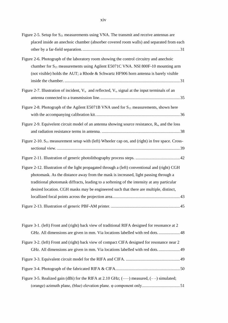
Figure 1-1. 2D illustration of the Chu sphere, with radius a, circumscribing the maximum
dimension of a generic antenna structure. For ka = 0.5, the enclosed volume equals
λ3/48π2. ................................................................................................................................. 5
Figure 1-2. Lower bound on Q plotted for three different values of radiation efficiency, (orange)
100%, (blue) 50%, (green) 5%. ............................................................................................ 8
Figure 1-3. Qratio vs ka value scatter plot for selected antennas from literature review; (orange-
diamond) antennas with measured radiation efficiency either reported or extractable from
data provided, (blue-circle) antennas with simulated radiation efficiency provided. Note
that for a linearly polarized ESA, the limit for Qratio is 1.5. ................................................ 14
Figure 1-4. Illustration of three types of antennas: (left) wire monopole, (top-right) inverted-L
antenna, and (bottom-right) inverted-F antenna. ................................................................ 20
Figure 1-5. Simulated S11 for (orange) monopole, (blue) ILA, and (green) IFA. The repective
resonance frequencies (and ka values) are 2.75 GHz (1.4), 3.00 GHz (0.78), and 3.75 GHz
(1.0). ................................................................................................................................... 22
Figure 2-1. CST MWS model and simulated radiation pattern (3D, directivity) of a typical
circular patch antenna, designed for resonance at 3 GHz (ka = 3.7). Color scheme: red
(max) – green – blue (min); max. directivity ≈ 7.5 dBi. .................................................... 26
Figure 2-2. CST MWS model and simulated radiation pattern (3D, directivity) of a typical half-
wave dipole antenna, designed for resonance at 3 GHz (ka = 1.4). Color scheme: red (max)
– green – blue (min); max. directivity ≈ 2.1 dBi. ............................................................... 26
Figure 2-3. Simulated direcitvity in (left) decibels and (right) linear scale, for the half-wave
dipole of Figure 2-2; (orange) azimuth plane, (blue) elevation plane; max. directivity ≈ 2.1
dBi or 1.6 (linear). .............................................................................................................. 27
Figure 2-4. Simulated direcitvity in decibels for (left) φ component, and (right) θ component,
for the half-wave dipole of Figure 2-2; (orange) azimuth plane, (blue) elevation plane.
Note that average magnitude for φ component is at-least 100 dB above that for θ
component. ......................................................................................................................... 30
xiv
Figure 2-5. Setup for S21 measurements using VNA. The transmit and receive antennas are
placed inside an anechoic chamber (absorber covered room walls) and separated from each
other by a far-field separation. ............................................................................................ 31
Figure 2-6. Photograph of the laboratory room showing the control circuitry and anechoic
chamber for S21 measurements using Agilent E5071C VNA. NSI 800F-10 mounting arm
(not visible) holds the AUT; a Rhode & Schwartz HF906 horn antenna is barely visible
inside the chamber. ............................................................................................................. 31
Figure 2-7. Illustration of incident, Vi, and reflected, Vr, signal at the input terminals of an
antenna connected to a transmission line. ........................................................................... 35
Figure 2-8. Photograph of the Agilent E5071B VNA used for S11 measurements, shown here
with the accompanying calibration kit. ............................................................................... 36
Figure 2-9. Equivelent circuit model of an antenna showing source resistance, Rs, and the loss
and radiation resistance terms in antenna. .......................................................................... 38
Figure 2-10. S11 measurement setup with (left) Wheeler cap on, and (right) in free space. Cross-
sectional view. .................................................................................................................... 39
Figure 2-11. Illustration of generic photolithography process steps. .......................................... 42
Figure 2-12. Illustration of the light propagated through a (left) conventional and (right) CGH
photomask. As the distance away from the mask is increased, light passing through a
traditional photomask diffracts, leading to a softening of the intensity at any particular
desired location. CGH masks may be engineered such that there are multiple, distinct,
locallized focal points across the projection area................................................................ 43
Figure 2-13. Illustration of generic PBF-AM printer. ................................................................. 45
Figure 3-1. (left) Front and (right) back view of traditional RIFA designed for resonance at 2
GHz. All dimensions are given in mm. Via locations labelled with red dots. .................... 48
Figure 3-2. (left) Front and (right) back view of compact CIFA designed for resonance near 2
GHz. All dimensions are given in mm. Via locations labelled with red dots. .................... 49
Figure 3-3. Equivalent circuit model for the RIFA and CIFA. ................................................... 49
Figure 3-4. Photograph of the fabricated RIFA & CIFA. ............................................................ 50
Figure 3-5. Realized gain (dBi) for the RIFA at 2.10 GHz; (–––) measured, (– –) simulated;
(orange) azimuth plane, (blue) elevation plane. φ component only.................................... 51

xv
Figure 3-6. Realized gain (dBi) for the RIFA at 2.10 GHz; (–––) measured, (– –) simulated;
(light-orange) azimuth plane, (light-blue) elevation plane. θ component only. ................. 51
Figure 3-7. Realized gain (dBi) for the CIFA at 2.10 GHz; (–––) measured, (– –) simulated;
(orange) azimuth plane, (blue) elevation plane. φ component only. .................................. 52
Figure 3-8. Realized gain (dBi) for the CIFA at 2.10 GHz; (–––) measured, (– –) simulated;
(light-orange) azimuth plane, (light-blue) elevation plane. θ component only. ................. 52
Figure 3-9. Measured radiation efficiency for (orange) CIFA, and (blue) RIFA; (–––) straight
connector (– –) right-angle connector. Plotted for ±10 MHz about resonance frequency. 54
Figure 3-10. Front views of the (left) CDIFAmSMP and (right) equivalent CIFAmSMP. All
dimensions are given in mm. Via locations labelled with red dots. ................................... 55
Figure 3-11. Photograph of the fabricated CDIFAmSMP mounted on a custom-made mSMP–SMA
adaptor. ............................................................................................................................... 56
Figure 3-12. S11 results for the CDIFAmSMP; (orange) measured, (blue) simulated; (– –) antenna
with feed structure, (···) antenna-only simulation; (grey) CIFAmSMP antenna-only
simulation. .......................................................................................................................... 57
Figure 3-13. Measured input impedance of the CDIFAmSMP; (orange) resistance, R, and (blue)
reactance, jX. Plotted for ±10 MHz around the resonant frequency. ................................. 57
Figure 3-14. Radiation efficiency of the CDIFAmSMP; (orange) measured, (blue) simulated; (– –)
antenna with feed structure simulation, (···) antenna-only simulation. Plotted for ±10 MHz
around resonance frequency. .............................................................................................. 58
Figure 3-15. Realized gain (dBi) for the CDIFAmSMP at resonance; (–––) measured, (– –)
simulated (antenna with feed structure); (orange) azimuth plane, (blue) elevation plane.
Combined absolute gain (φ and θ components). ................................................................ 59
Figure 3-16. Photograph of two fabricated CDIFASMP and Molex series 73386 SMP–SMA
adaptor. ............................................................................................................................... 60
Figure 3-17. S11 results for the CDIFASMP; (orange) measured, (blue) simulated; (– –) antenna
with SMP solder pad simulation, (···) antenna-only simulation. ....................................... 61
Figure 3-18. Radiation efficiency for the CDIFASMP; (orange) measured, (blue) simulated; (–––)
measurement with Wheeler cap box in parallel alignment, (– · –) measurement with
Wheeler cap box in diamond alignment; (···) simulation for antenna with SMP solder pad,
(– –) simulation for antenna-only. Plotted for ±10 MHz around resonance frequency. ..... 62

xvi
Figure 3-19. Realized gain (dBi) for the CDIFAmSMP at resonance; (–––) measured, (– –)
simulated (antenna with solder pad); (orange) azimuth plane, (blue) elevation plane.
Combined absolute gain (φ and θ components). ................................................................. 63
Figure 3-20. Illustration of the current paths on an (top) IFA and (bottom) PIFA. The ground
plane acts to reflect the EM waves born of these currents, and create the so-called ‘image
antenna’. .............................................................................................................................. 65
Figure 3-21. Front views of the (top) CDPIFA, (bottom-left) CPIFA2A, and (bottom-right)
CPIFA1A. Red and Cyan dots designate position of feed point and shorting pin,
respectively. Note that maximum overall dimension of all simulated and fabricated models
is 50 mm. ............................................................................................................................ 66
Figure 3-22. Photographs of the fabricated (left) CDPIFA and (right) CPIFA2A. ....................... 66
Figure 3-23. Simulated S11 for (orange) CDPIFA, (blue) CPIFA2A, and (green) CPIFA1A. ........ 68
Figure 3-24. Simulated S11 for CDPIFA, parameterised ang_f. Legend shown to the right, units
are degrees (°). Original parameter combination shown in orange. .................................... 69
Figure 3-25. Simulated S11 for CDPIFA, parameterised ang_s. Legend shown to the right, units
are degrees (°). Original parameter combination shown in orange. .................................... 69
Figure 3-26. Simulated S11 for CDPIFA, parameterised ang_t. Legend shown to the right, units
are degrees (°). Original parameter combination shown in orange. .................................... 70
Figure 3-27. Simulated S11 for CDPIFA, parameterised l_gap. Legend shown to the right, units
are mm. Original parameter combination shown in orange. ............................................... 70
Figure 3-28. S11 results for CDPIFA; (orange) measured, (blue) simulated. .............................. 71
Figure 3-29. S11 results for CPIFA2A; (orange) measured, (blue) simulated. .............................. 71
Figure 3-30. Peak normalized radiation pattern (dBi) for the CDPIFA; (top) 1st resonance,
(bottom) 2nd resonance; (left) φ component, (right) θ component; (–––) measured, (– –)
simulated; (orange) azimuth plane, (blue) elevation plane. ................................................ 72
Figure 3-31. Peak normalized radiation pattern (dBi) for the CPIFA2A; (top) 1st resonance,
(bottom) 2nd resonance; (left) φ component, (right) θ component; (–––) measured, (– –)
simulated; (orange) azimuth plane, (blue) elevation plane. ................................................ 73
Figure 3-32. Mean* simulated gain for the CDPIFA as a function of frequency; (purple) φ
component, (green) θ component, (red-dashed) combined total. ........................................ 74
Figure 3-33. Mean* simulated gain for the CPIFA2A as a function of frequency; (purple) φ
component, (green) θ component, (red-dashed) combined total. ........................................ 74

xvii
Figure 4-1. (left) Front and (right) back view of compact CDIFALC, showing the dimensions p
and q which fully describe the simplified digitated structure. All dimensions are given in
mm. Via locations labelled with red dots. .......................................................................... 80
Figure 4-2. Equivalent circuit model for the CDIFALC. Addition of digitated structure increases
the self-inductance and self-capacitance of the antenna. .................................................... 80
Figure 4-3. Simulated resonance frequency of CDIFA for varying dimensions of p and q in mm.
............................................................................................................................................ 81
Figure 4-4. Simulated ka of CDIFA for varying dimensions of p and q in mm. ........................ 82
Figure 4-5. Simulated radiation efficiency of CDIFA for varying dimensions of p and q in mm.
............................................................................................................................................ 83
Figure 4-6. Simulated mean* realized gain of CDIFA for varying dimensions of p and q in mm.
............................................................................................................................................ 83
Figure 4-7. Photograph of the various fabricated CDIFALC (top; left to right) CDIFAL1C1,
CDIFAL1C2, CDIFAL1C3; (middle; left to right) CDIFAL2C1, CDIFAL2C2, CDIFAL2C3;
(bottom; left to right) CDIFAL3C1, CDIFAL3C2, CDIFAL3C3. ............................................... 84
Figure 4-8. Range of frequencies where measured S11 ≤ −3 dB for the various CDIFALC as listed
in Table 4-1. Corresponding FBW−3dB is marked as percentage. ....................................... 86
Figure 4-9. Photographs of Wheeler cap measurement setup, (left) side length 10 cm in diamond
alignment, (right) side length 5 cm in parallel alignment. ................................................. 87
Figure 4-10. Different adaptors used to feed antennas for efficiency measurements: i) 4 cm bare,
ii) 4 cm covered, iii) 4 cm covered, iv) 8 cm bare, v) 8 cm covered. ................................. 87
Figure 4-11. Measured radiation efficiency for the CDIFAL1C1, using 4 cm adaptor; (orange) box
parallel aligned, (blue) box diamond aligned. Plotted for ±10 MHz around resonance
frequency. ........................................................................................................................... 88
Figure 4-12. Measured radiation efficiency for the CDIFAL1C1; (orange) 4 cm adaptor, (blue)
other 4 cm adaptor, (green) 8 cm adaptor. Plotted for ±10 MHz around resonance
frequency. ........................................................................................................................... 89
Figure 4-13. Measured radiation efficiency for the CDIFAL1C1; (blue) 4 cm adaptor without
ferrite sleeves, (green) 8 cm adaptor without ferrite sleeves; (orange) (===) 4 cm adaptor
with ferrite sleeves. Plotted for ±10 MHz around resonance frequency. ........................... 90
Figure 4-14. (orange-square) Simulated radiation efficiency, and (blue-circle) simulated
resonance frequency for the CDIFAL1C1, for varying lengths of coaxial cable (cm);

xviii
simulation is carried out using bare coaxial cable only to model the adaptor – no ferrite
sleeves are modelled. .......................................................................................................... 90
Figure 4-15. Measured radiation efficiency for the CDIFAL1C1; (orange) 4 cm straight
terminated adaptor, (blue) 4 cm right-angle terminated adaptor. Plotted for ±10 MHz
around resonance frequency. .............................................................................................. 91
Figure 4-16. Photograph of AUT mounted on NSI 800F-10 Z-arm inside anechoic chamber. .. 93
Figure 4-17. Realized gain (dBi) for the CDIFAL1C1 at 1.94 GHz; (–––) measured, (– –)
simulated; (orange) azimuth plane, (blue) elevation plane. φ component only. ................. 94
Figure 4-18. Realized gain (dBi) for the CDIFAL1C1 at 1.94 GHz; (–––) measured, (– –)
simulated; (light-orange) azimuth plane, (light-blue) elevation plane. θ component only. 94
Figure 4-19. Realized gain (dBi) for the CDIFAL2C2 at 1.68 GHz; (–––) measured, (– –)
simulated; (orange) azimuth plane, (blue) elevation plane. φ component only. ................. 95
Figure 4-20. Realized gain (dBi) for the CDIFAL2C2 at 1.68 GHz; (–––) measured, (– –)
simulated; (light-orange) azimuth plane, (light-blue) elevation plane. θ component only. 95
Figure 4-21. Realized gain (dBi) for the CDIFAL3C3 at 1.16 GHz; (–––) measured, (– –)
simulated; (orange) azimuth plane, (blue) elevation plane. φ component only. ................. 96
Figure 4-22. Realized gain (dBi) for the CDIFAL3C3 at 1.16 GHz; (–––) measured, (– –)
simulated; (light-orange) azimuth plane, (light-blue) elevation plane. θ component only. 96
Figure 4-23. Simulated (top) radiation efficiency and (bottom) S11 for the (blue) CDIFA433MHz,
(orange) CDIFA2.4GHz, and (green) CDIFA5.9GHz. ................................................................ 99
Figure 4-24. Qratio vs ka value scatter plot for CDIFASMP (yellow-square) and CDIFALC (green-
triangle), with selected antennas from literature review for comparison (c.f. Figure 1-3).
.......................................................................................................................................... 100
Figure 4-25. (–––) Measured and (– –) simulated S11 results for the CDIFAL1C1 (orange),
CDIFAL2C2 (blue), CDIFAL3C3 (green). ............................................................................. 101
Figure 4-26. Qratio vs ka value scatter plot for CDIFALC computed using (green-triangle)
measured and (red-triangle) simulated FBW-3dB and ηr, with selected antennas from
literature review for comparison (c.f. Figure 1-3). ........................................................... 102
Figure 5-1. Front view of MLA model, (yellow) metal, (teal) substrate; ground plane extents are
shown with a patterned fill. ............................................................................................... 107

xix
Figure 5-2. Simulated S11 for MLA, parameterised hground. Legend shown to the right, units are
mm. Original parameter combination shown in orange. .................................................. 108
Figure 5-3. Simulated S11 for MLA, parameterised strack. Legend shown to the right, units are
mm. Original parameter combination shown in orange. .................................................. 109
Figure 5-4. Simulated S11 for MLA, parameterised iloop. Legend shown to the right, units are
mm. Original parameter combination shown in orange. .................................................. 109
Figure 5-5. Simulated S11 for MLA, parameterised wloop. Legend shown to the right, units are
mm. Original parameter combination shown in orange. .................................................. 110
Figure 5-6. Photograph of the manufactured MLA, mounted on an SMA connector (solder not
yet applied). ...................................................................................................................... 111
Figure 5-7. S11 results for the MLA; (orange) measured, (blue) simulated; (– –) simulation with
optimized parameters, (···) simulation with all track widths reduced by 35%. ............... 112
Figure 5-8. Realized gain (dBi) for the MLA at 2.2 GHz; (–––) measured φ component, (– –)
simulated φ component, (···) simulated θ component; (orange) azimuth plane, (blue)
elevation plane.................................................................................................................. 113
Figure 5-9. CST MWS 3D model of (left) MHDAA and (right) MHDAB; grey tracks are
metallizations (PEC). ....................................................................................................... 115
Figure 5-10. Photograph of 3D dome antenna, MHDAA, mounted in ancheoic chamber for
radiation pattern measurements. ....................................................................................... 115
Figure 5-11. S11 for (orange) MHDAA; (–––) measured and (– –) simulated. .......................... 116
Figure 5-12. S11 for (blue) MHDAB; (–––) measured and (– –) simulated. Simulated curve for
(green) MHDAB with straight microstrips is also included. ............................................. 117
Figure 5-13. Peak normalized radiation pattern (dBi) for the MHDAA; (left) θ component,
(right) φ component; (–––) measured, (– –) simulated; (orange) azimuth plane, (blue)
elevation plane. Cross-polar at least 15 dB below co-polar. ............................................ 118
Figure 5-14. Peak normalized radiation pattern (dBi) for the MHDAB, measured at 520 MHz;
(left) θ component, (right) φ component; (–––) measured, (– –) simulated; (orange)
azimuth plane, (blue) elevation plane. Cross-polar at least 15 dB below co-polar. ......... 118
Figure 5-15. Peak normalized radiation pattern (dBi) for the MHDAB, measured at 710 MHz;
(left) θ component, (right) φ component; (–––) measured, (– –) simulated; (orange)
azimuth plane, (blue) elevation plane. Cross-polar at least 10 dB below co-polar. ......... 119

xx
Figure 5-16. Cross-sectional view of CAD models simulated in CST MWS, for progressively
greater voluminous expansion. ......................................................................................... 121
Figure 5-17. Simulated resonance frequency of (orange) 1st and (blue) 2nd resonances as a
function of h. Fabricated antennas are annotated. ............................................................. 122
Figure 5-18. Simulated radiation efficiency of (orange) 1st and (blue) 2nd resonances as a
function of h. Fabricated antennas are annotated. ............................................................. 122
Figure 5-19. Photograph of antenna part (material: titanium alloy) fabricated using SLM PBF-
AM. ................................................................................................................................... 124
Figure 5-20. Photograph of antenna part (material: titanium alloy) fabricated using SEBM PBF-
AM. ................................................................................................................................... 124
Figure 5-21. Photograph of two SEBM PBF-AM fabricated antenna prototypes, shown
assembled; (left) full-spherical, (right) flat. ...................................................................... 125
Figure 5-22. S11 results for PBF-AM flat CDPIFA; (orange) measured, (blue) simulated.
Radiation efficiency at respective resonance frequencies, for the 2nd resonance; (purple)
measured, (green) simulated. ............................................................................................ 127
Figure 5-23. S11 results for PBF-AM part-spherical CDPIFA; (orange) measured, (blue)
simulated. Radiation efficiency at respective resonance frequencies, for the 2nd resonance;
(purple) measured, (green) simulated. .............................................................................. 128
Figure 5-24. S11 results for PBF-AM full-spherical CDPIFA, sample A; (orange) measured,
(blue) simulated. Radiation efficiency at respective resonance frequencies, for the 2nd
resonance; (purple) measured, (green) simulated. ............................................................ 128
Figure 5-25. S11 results for PBF-AM full-spherical CDPIFA, sample B; (orange) measured,
(blue) simulated. Radiation efficiency at respective resonance frequencies, for the 2nd
resonance; (purple) measured, (green) simulated. ............................................................ 129
Figure 5-26. Realized gain (dBi) for the full-spherical ESA at 1.7 GHz; (orange) measured –
sample A, (green) measured – sample B, (blue) simulated; azimuth plane. Combined
absolute gain (φ and θ components). ................................................................................ 130
Figure 5-27. Realized gain (dBi) for the full-spherical ESA at 1.7 GHz. (orange) measured –
sample A, (green) measured – sample B, (blue) simulated; elevation plane. Combined
absolute gain (φ and θ components). ................................................................................ 131
Figure 5-28. Simulated resonance frequency of (orange) 1st and (blue) 2nd resonances as a
function of h. Extremes are annotated. ............................................................................. 132

xxi
Figure 5-29. Simulated radiation efficiency of (orange) 1st and (blue) 2nd resonances as a
function of h. Extremes are annotated. ............................................................................. 133
Figure 5-30. Photograph of unused antenna part fabricated using SEBM PBF-AM, illustrating
the improvement to surface finish through process optimization (c.f. Figure 5-20). ....... 134

xxii
(This page intentionally left blank.)

xxiii
List of Tables
Table 3-1. Summary of average forward measured gain (±90°) for the RIFA and CIFA. All
values are presented in dBi. ................................................................................................ 53
Table 3-2. Comparison of simulated mean gain and radiation efficiency for the CDPIFA and
CPIFA2A. ............................................................................................................................ 75
Table 4-1. Parameter combinations and resonant frequencies of the fabricated CDIFALC. ....... 85
Table 4-2. Radiation efficiency, ηr (%) of various AUTs at resonance. ..................................... 92
Table 4-3. Q, Qlb and Qratio of various AUTs at resonance.......................................................... 92
Table 4-4. Summary of average forward measured gain (±90°) for the CDIFAL1C1, CDIFAL2C2,
and CDIFAL3C3. All values are presented in dBi. ............................................................... 97
Table 5-1. Parameter list for optimized MLA. .......................................................................... 107
Table 5-2. Simulated and measured resonant frequency and radiation efficiency at 2nd resonance
for PBF-AM fabricated CDPIFAs. ................................................................................... 129

xxiv
(This page intentionally left blank.)

xxv
Nomenclature
2D Two dimensional
3D Three dimensional
4D Four dimensional
AM Additive manufacturing
AUT Antenna under test
CAD Computer aided design
CDIFA Circular, digitated inverted-F antenna
CDPIFA Circular, digitated planar inverted-F antenna
CGH Computer generated hologram/holographic/holography
CIFA Circular inverted-F antenna
CNC Computer numerical control
CPIFA Circular planar inverted-F antenna
CPW Co-planar waveguide
CST MWS CST Microwave Studio
dB Decibel(s)
dBi Decibels over isotropic
DRA Dielectric resonator antenna
EM Electromagnetic
ESA Electrically small antenna
FBW Fractional bandwidth
GPS Global positioning system
HIS High impedance surface
IFA Inverted-F antenna
ILA Inverted-L antenna

xxvi
IoT Internet of Things
MHDA Meanderline hemispherical dome antenna
MLA Meanderline antenna
NIC Negative impedance converter
PBF Powder bed fusion
PCB Printed circuit board
PEC Perfect Electrical Conductor
PIFA Planar inverted-F antenna
RF Radiofrequency
RIFA Rectangular inverted-F antenna
RL Return loss
SEBM Selective electron beam melting
SGA Standard gain antenna
SLA Stereolithography apparatus (type of AM)
SLM Selective laser melting
SNR Signal-to-noise ratio
STL Stereolithography
VNA Vector network analyzer
a Radius of an imaginary sphere circumscribing the
maximum dimension of the antenna
C Capacitance/capacitor
D Directivity
FBW-3dB Half power fractional bandwidth
fC Centre frequency
fh Upper frequency

xxvii
fl Lower frequency
G Gain
Gr Realized gain
k Wavenumber
L Inductance/inductor
M Impedance mismatch factor
P Polarization mismatch factor
PAUT Power received by AUT
Pi Incident signal power
Pin Input (accepted) power
Pr Reflected signal power
Prad Power radiated
PSGA Power received by SGA
Q Quality factor (of antenna)
Qlb Lower bound on Q
Qlb-Chu Lower bound on Q, derived from the work of Chu, Lan
Jen
Qratio Ratio of quality factor of antenna under test to the
fundamental minimum limit on quality factor for an
antenna of the same geometry and radiation efficiency
R Resistance/resistor
RA Total resistance of antenna
Rloss Loss resistance
Rrad Radiation resistance
RS Source resistance
S11 Ratio of reflected to incident wave voltage at port 1 (in
two-port VNA)
S21 Ratio of reflected wave voltage at port 2 to incident wave
voltage at port 1 (in two-port VNA)

xxviii
SFS S11 for antenna in free space
SWC S11 for antenna enclosed in Wheeler cap
tanδ Loss tangent
U0 Radiation intensity of an isotropic source radiating the
same power as AUT
Ui Radiation intensity of an isotropic source operating at the
same input power as AUT
Umax Maximum radiation intensity
Vi Incident signal voltage
Vr Reflected signal voltage
XA Total reactance of antenna
XC Capacitive reactance
XL Inductive reactance
ZA Input impedance of antenna
ZNA Normalized input impedance of antenna
ZTL Characteristic impedance of the transmission line
Γ Voltage reflection coefficient
εr Relative permittivity
ηr Radiation efficiency
θ Angle in the z-x plane
λ Wavelength
σ Conductivity
φ Angle in the x-y plane

Chapter 1 1
CHAPTER 1
Introduction
Miniaturization is perhaps the defining trend in the design and manufacture of
modern electronics. Spurred by the demand for ever higher productivity and
mobility, the constituent parts of modern electronic devices are encouraged to
take an ever-smaller form factor. Central processing units have traditionally
received the most attention towards this aim, governed loosely by the well-
known Moore’s Law [1-4], though the philosophy has since been extended to
entire systems [5]. Historically, process resolutions (fabrication) and heat
dispersal have been the primary hurdles; the trend is so mature that limits on
miniaturization are now believed to be set by quantum tunnelling effects present
at the molecular level [6, 7]. Batteries and power sources have similarly
improved leaps and bounds to keep up pace [8-10].
For electronics relying on wireless connectivity, small antennas are vitally
important. In some cases, the antenna even determines the absolute limits on
system performance [5, 11]; the miniaturization of these antennas in a similar
vein to other electronics components is responsible for the continued
development and deployment of ever more sophisticated wireless
communications systems and the modern ‘information’ economy. The original
debate over wired versus wireless networks in terms of safety, range, set-up and
operational costs, and so forth is as valid as ever. However, the boom in personal
computing and communication devices, together with the rise in popularity of
‘smart’ gadgets – all linked together with the Internet of Things (IoT) – has led
to a paradigm shift in the preference of wireless communications over wired
[12], due in part to the desire for connectivity at all times and places. Indeed, in
many applications, real estate is a prime commodity and wireless networks

Chapter 1 2
employing small antennas are the only viable option; examples include personal
communication gadgets (for the sake of portability), healthcare monitoring
equipment (for the safety and comfort of the patient), and even military
equipment (for ease of concealment). Novel security measures for wireless
communications – such as directional modulation [13, 14] – address a relative
disadvantage of wireless communications, helping to ensure the continuation of
this trend.
Pioneered by Hertz in 1888 and popularized by Marconi in 1901 [15, 16], an
antenna is a device which interfaces free space electromagnetic (EM) radiation,
specifically radio waves, with guided waves (waveguides) or electrical energy
(circuits), and vice versa. In essence, these are conductive structures engineered
to ‘resonate’ at a particular frequency of operation; their physical dimensions
are consequently determined primarily by the wavelength at this operational
frequency, related by a physical constant – the speed of light in the medium of
operation (often free space). To take only a few examples and typical
frequencies, the global positioning system (GPS) operates at a typical frequency
of 1.5 GHz, 3G and 4G mobile phone systems at 800 MHz, and Wi-Fi and
Bluetooth at 2.4 GHz; wavelengths (in free space) at these frequencies are
approximately 20 cm, 38 cm, and 13 cm, respectively. For comparison, a typical
‘smart’ watch has a maximum dimension of 4 cm [17]. Thus, many practical
small antennas used in mobile (especially handheld) wireless devices are classed
as electrically small – that is, operating at wavelengths several times larger than
their physical size.
Research in the field of electrically small antennas (ESA) is centred around the
same aims which govern the miniaturization of electronics in general: improved
performance for a fixed area/volume, and preventing performance degradation
as the volume is shrunk. Consequently, ESAs are most often discussed in terms
of their fundamental performance limitations; the field was popularized by a
seminal paper authored by Harold Wheeler in 1947 titled ‘Fundamental
Limitations of Small Antennas’ [18]. These limitations, expanded later in this
Thesis, are low efficiency, narrow bandwidth, and a poor impedance match to
the rest of the radiofrequency (RF) front-end [11, 19-22]. As explained later,

Chapter 1 3
novel three-dimensional (3D) antenna designs may be employed to overcome
some of these limitations [11, 19-22]; structures hitherto too complex to
fabricate with traditional processes may soon be realized with emergent
technologies such as holographic photolithography and three dimensional (3D)
printing [23-25].
1.1. Thesis Structure
This Thesis documents research conducted by the author towards practical
antenna design, encompassing modifications to the antenna’s structure to
optimize performance, as well as an investigation of novel manufacturing
techniques.
Chapter 1 – Introduction – covers the formal definitions of ESAs, and the
theoretical and practical limitations on the design of ESAs. This is followed by
a literature review of popular and recent antenna designs, grouped by various
miniaturization techniques. The chapter concludes with a review of the aims and
motivations of this research.
Chapter 2 – Theoretical Background for Electrically Small Antennas –
covers the various performance metrics used throughout the document to
analyse antennas, as well as the measurement techniques and setups used. The
second part of the chapter provides an overview of manufacturing processes for
antennas, from the traditional photolithography to the emergent 3D printing.
Chapter 3 – Miniaturization using Centrally Populated Digitated Structure
– covers the design and analysis of two novel ESAs: single resonance inverted-
F antenna (IFA), and dual resonance planar inverted-F antenna (PIFA).
Simulation and measurement results are provided to illustrate the effects of
miniaturization on the antenna’s performance; practical considerations for the
accurate measurement of radiation efficiency are highlighted.
Chapter 4 – Detailed Analysis of Centrally Populated Digitated Structure –
provides an in-depth analysis of the novel contribution leading to miniaturized

Chapter 1 4
antennas. An abstraction of the centrally populated digitated structure is
introduced for the sake of simplicity, and an extensive parameter study provided
to aid rapid design tuning of the digitated IFA. Finally, antenna performance is
compared to some recent antennas discussed in the literature review.
Chapter 5 – Investigation of Fabrication Techniques – covers three antenna
types fabricated in-house as part of a concurrent investigation of fabrication
techniques. Pioneering measured results for 3D printed metallic antennas are
provided; the advantages and limitations of this emergent fabrication technique
in the context of antenna fabrication are also discussed.
Chapter 6 – Conclusions – concludes this Thesis. Limitations of the work
undertaken are highlighted, and recommendations are made for the refinement
of current results, as well as the exploration of related lines of research.
The appendix – Computer Generated Holograms – provides a summary of
the work undertaken during the early stages of this project towards the
realization of holographic photolithography.
1.2. Definition of Small Antennas
In order to distinguish between the physical and electrical size of an antenna, its
dimensions are expressed in terms of the operating wavelength (or frequency);
generally, the largest dimension of an ESA is a small fraction (typically a tenth)
of its operating wavelength. A precise definition is not available in the IEEE
Standard for Definitions of Terms for Antennas [26], and thus there are more
than one practical definitions considered by the antenna research community. A
widely accepted definition for as ESA is one whose maximum dimension is less
than or equal to λ/2π, referred to as a radianlength (where λ is the symbol for
wavelength) [19, 20]. Antenna geometries abiding by this demarcation radiate
the first order spherical modes of a small Hertzian dipole [20] – an infinitesimal
theoretical construct which provides the basis for the analysis of more
complicated antenna geometries. Throughout this Thesis, a popular equivalent
formulation is used:
Chapter 1 5
𝑘𝑎 ≤ 0.5
Equation 1-1
where k is the wavenumber (equal to 2π/λ), and a is the radius of an imaginary
sphere circumscribing the maximum dimension of the antenna, also referred to
as the Chu sphere in acknowledgement of the seminal work on the fundamental
limitations of ESAs carried out by Chu in 1948 [27]. This is illustrated in Figure
1-1. If the antenna is mounted on a very large ground plane, then by default the
Chu sphere will incorporate the ‘image’ of the antenna within the ground plane;
the actual dimension of the ground plane need not be incorporated into the
parameter a. However, it becomes necessary to include the entire structure in
consideration for a if the ground plane is comparatively sized to the antenna, or
is deliberately designed to affect the antenna’s performance (e.g. defected
ground structures).
Another commonly used definition for ESAs is 𝑘𝑎 ≤ 1, so that the radius and
not the diameter of the antenna equals one radianlength. Such an antenna would
Figure 1-1. 2D illustration of the Chu sphere, with radius a, circumscribing the
maximum dimension of a generic antenna structure. For ka = 0.5, the enclosed
volume equals λ3/48π2.
radius = a
Chu
sphere
∼

Chapter 1 6
be enclosed in a radiansphere, which represents the boundary between the near-
and far-field radiation for a small Hertzian dipole [20, 28].
As such, a physically small antenna of maximum dimension 5 cm (i.e. a = 2.5
cm) would be considered electrically small if operating at 1 GHz (ka = 0.5), but
not if operating at 3 GHz (ka = 1.6). In general, the performance of an antenna
will suffer as it is forced to operate in the region where it would be considered
electrically small.
1.3. Fundamental Limitations of Electrically Small Antennas
As the electrical size of an antenna is reduced, its radiation pattern tends towards
that of a Hertzian (very small) dipole [19, 20], and is therefore not a property
that can be engineered towards specifications. Note that the radiation pattern of
a Hertzian dipole is similar to that of the half-wave dipole shown in Figure 2-2
(with maximum directivity ≈ 1.8 dBi* instead of 2.1 dBi). In fact, most
applications requiring ESAs often tend to demand omni-directional patterns;
handheld and body-mounted devices, for instance, may be positioned in any
number of orientations during use. Additionally, many modern wireless devices
are employed in environments polluted with scattered and multipath fields,
resulting in received signals arriving from multiple directions and with varying
polarizations. The polarization mismatch factor, P (≤1), is thus often ignored in
the analysis of ESAs. Due to this limitation on directivity, and the non-
consideration of polarization mismatch, a good impedance match and high
radiation efficiency are the main influences on antenna gain which can be
engineered towards a specific target. These are often combined into a single
metric called the Qratio, described here.
The quality factor, Q, of an antenna can be related to its impedance match and
fractional bandwidth (FBW):
* dBi is decibels over isotropic (see Chapter 2).

Chapter 1 7
𝑄𝑎𝑛𝑡𝑒𝑛𝑛𝑎 =(𝑉𝑆𝑊𝑅−3𝑑𝐵 − 1)
𝐹𝐵𝑊−3𝑑𝐵√𝑉𝑆𝑊𝑅−3𝑑𝐵
Equation 1-2
This relationship is explained in greater detail in Chapter 2, with Equation 1-2
repeated as Equation 2-26. Considerable work has been carried out on the
theoretical performance limitations of ESAs, resulting in the formulation of key
limits on the lower bound of Q, termed Qlb. These limits can be formulated in
terms of the electrical size and radiation efficiency of the antenna, as presented
in Equation 1-3. A specialized figure of merit, namely the Qratio (which is simply
the ratio of the Q of an antenna over its theoretical lower bound), is therefore a
useful way of quantifying the performance of any ESA. It also allows for an
easier comparison across various ESA topologies and designs.
The earliest work on fundamental limitations of ESAs was conducted by
Wheeler in 1947 [18], refined subsequently by Chu [27] and McLean [29],
amongst others [30-33]; see [20] for a summary of major contributions to this
line of research. For linearly polarized, single-mode antennas, the following
expression for the lower bound on Q (the Chu limit) is commonly used [19]:
𝑄𝑙𝑏−𝐶ℎ𝑢 = 𝜂𝑟 (1
(𝑘𝑎)3+
1
𝑘𝑎)
Equation 1-3
where ηr is the radiation efficiency of the antenna (see Chapter 2).
The lower bound for Q is plotted in Figure 1-2 for three different values of
radiation resistance. The corresponding limit for a circularly polarized antenna
is approximately half of this limit [20]. The main implication is that there are
fundamental upper limits on the radiation efficiency and/or bandwidth for a
given size of antenna; moreover, as the electrical size of the antenna is reduced,
the quality factor tends to increase. Considering again the imaginary Chu sphere
illustrated in Figure 1-1, work by Wheeler and others has also indicated that for
the same maximum dimension, an antenna fully utilizing the available volume

Chapter 1 8
has the lowest Q compared to any other geometries within the same volume [11,
19, 20]. In other words, the ‘best’ compromise between the occupied volume,
bandwidth, and efficiency is realized when most of the available volume is
utilized for the radiating structure. Much of the work mentioned focuses on
establishing an upper limit on the bandwidth (so that the bandwidth is expressed
as a function of the lower bound on Q), as ESAs typically exhibit very narrow
fractional bandwidths, down to a few percent [19]. Considered in isolation, high
radiation efficiencies (ηr ≥ 90% [19]) are possible with the use of highly efficient
conductors and a very good impedance match at resonance, though the resulting
bandwidth is inevitably narrow.
From Equation 1-2 and Equation 1-3, an expression for Qratio can be derived:
𝑄𝑟𝑎𝑡𝑖𝑜 =𝑄𝑎𝑛𝑡𝑒𝑛𝑛𝑎
𝑄𝑙𝑏−𝐶ℎ𝑢=
(𝑉𝑆𝑊𝑅−3𝑑𝐵 − 1)(𝑘𝑎)3
(𝐹𝐵𝑊−3𝑑𝐵√𝑉𝑆𝑊𝑅−3𝑑𝐵)(1 + (𝑘𝑎)2)(𝜂𝑟)
Equation 1-4
Large parts of Chapter 3 and the entirety of Chapter 4 deal with linearly
polarized ESAs, with a single impedance resonance within the antenna’s
fractional bandwidth. Under these conditions, the expression for Qratio given in
Figure 1-2. Lower bound on Q plotted for three different values of radiation
efficiency, (orange) 100%, (blue) 50%, (green) 5%.
0.1
1
10
100
0 0.5 1 1.5 2
Qlb
-Ch
u
ka

Chapter 1 9
Equation 1-4 is valid and therefore included in the discussion. However, parts
of Chapter 3 and Chapter 5 deal with ESAs where the intent is to tune two
resonances close together such that they fall within a single fractional bandwidth
(as a means of further increasing bandwidth). There is still no consensus as to
what fundamental limits apply to such antennas [19, 34], and therefore the
parameter Qratio is not used in the discussion of such antennas.
1.3.1. Practical Design Considerations
It can be observed from Equation 1-2 that the Q of an antenna is inversely related
to its fractional bandwidth, and from Equation 1-3 that the degree of
miniaturization (note that this is the inverse of ka) is inversely related to the
antenna’s radiation efficiency, through a lower bound for Q. It is also
understood from Equation 1-5 (note: repeated as Equation 2-22 in Chapter 2
where radiation efficiency is formally defined) that a high radiation resistance,
Rrad, leads to a higher radiation efficiency.
𝜂𝑟 =𝑃𝑟𝑎𝑑
𝑃𝑖𝑛=
𝑃𝑟𝑎𝑑
𝑃𝑟𝑎𝑑 + 𝑃𝑙𝑜𝑠𝑠=
𝑅𝑟𝑎𝑑
𝑅𝑟𝑎𝑑 + 𝑅𝑙𝑜𝑠𝑠=
𝑅𝑟𝑎𝑑
𝑅𝐴
Equation 1-5
Therefore, it is important not only to match the resistive component of an
antenna, RA, to 50 Ω (in a typical 50 Ω system), but also to ensure that Rrad and
not Rloss (loss resistance) is the main contributor to RA. This is particularly
challenging since electrically small antennas tend to have a low radiation
resistance, with a large reactive component of impedance [19].
From this discussion, it is clear that miniaturization is at odds with performance.
Bandwidth and radiation efficiency are the two key properties which may be
improved (within fundamental limitations), though there is often a trade-off
between miniaturization and performance depending on the application at hand.
For instance, it is a known practice to purposefully mismatch an ESA to obtain
marginal improvements in its bandwidth [19], a practice not immediately
obvious from the metric Qratio. Narrower bandwidth antennas are more
susceptible to frequency detuning from nearby objects (due to narrow

Chapter 1 10
bandwidths, a slight shift in the resonance frequency from the actual operational
frequency could significantly increase the mismatch factor).
Taking a broader view still, material considerations and even ease of
manufacture all play a big part in the final structure and make up of an antenna.
Cell phone antennas, for example, have transitioned from monopole whip
antennas encased in radomes and strategically placed away from the main phone
circuitry to complex configurations often printed on the same printed circuit
board (PCB) as the rest of the electronic circuitry. It would not be a wild claim
to make that material losses due to the dielectric of the PCB are unavoidable for
practical modern antennas. Despite the knowledge that utilizing the full
available volume (theoretically) generally improves antenna performance [11,
19, 20], it might not be practical to design such an antenna where the real estate
is simply not available for voluminous structures. There are questions over
whether standard manufacturing techniques can be suitably adapted to the
manufacture of such antenna structures. Solutions may be found via the use of
novel fabrication techniques, such as 3D printing, though it is yet unclear if such
processes can deliver to the tolerance levels expected by antenna designers all
the way through to the end-user.
1.4. Literature Review
This section provides a non-exhaustive list of common miniaturization
techniques for the design of ESAs, grouped by the type of materials, structures,
and/or components required. Often, two or more of these techniques are
combined for the design of practical ESAs. This is highlighted in an overview
of recently reported ESAs, and a case study on the evolution of the IFA from a
wire monopole. For a more extensive survey of influential ESAs, refer to [11],
[20], and [35].
1.4.1. Common Miniaturization Techniques
Miniaturizing may be viewed from two perspectives, which are often combined
for practical antenna design. The first is to simply lower the resonance
Chapter 1 11
frequency for an antenna of given dimensions (i.e. same physical size). Often,
care is taken to minimize the deterioration in the performance of the antenna as
its electrical size is reduced. Another approach is to improve the performance
of an antenna for a given electrical size, in terms of its impedance match,
radiation efficiency, and fractional bandwidth. (It should be noted that the
electrical size is defined by the largest dimension and its circumscribing sphere;
however, expansion into the 3rd dimension is not always a practical option.)
As explained later in Chapter 2, a well matched resonant antenna has no reactive
component in its feed point impedance, with the resistive component matched
to that of the feed line (cable). Note that it is still possible to impedance match
antennas where the condition of zero net reactance is not satisfied through the
antenna geometry itself, with the use of a capacitor or inductor, as required, to
tune the perceived feed point reactance to zero [19, 20]. These passive
components may be integrated into the geometry of the antenna itself (for
instance chip capacitors may be directly soldered onto tracks on a PCB), or used
to create an external two-port (i.e. one input, one output) matching network.
Such reactive components may theoretically be used to tune any antenna to
resonance at a desired operational frequency, thereby resulting in an electrically
small radiator. Practical usage of this technique, however, is limited by the range
of frequencies over which matching is required, and the degree to which
additional losses are introduced by the matching components [11, 19, 20]. That
is, any gains made by an improved mismatch factor may well be negated by the
extra losses incurred due to these matching components. The complexity of
fabrication is also increased leading to slower throughput and increased costs.
Wideband matching is possible with the use of negative impedance converters
(NIC) [11, 20, 36]. These are two-port networks comprised of a combination of
active devices (diodes) with the usual passive reactive components, and
designed to cancel out the reactive part of an antenna’s impedance over a wide
band of frequencies. A biasing DC voltage is required for the active
components, thereby increasing the energy drain. Moreover, such an external
matching network would need to be considered as part of the antenna structure,
effectively raising the ka value of the antenna to be miniaturized.

Chapter 1 12
An alternative technique to achieve the same tuning effect is the clever use of
geometry, shaping the antenna structure such that equivalent inductance or
capacitance is added to its feed point impedance. One approach to reducing the
resonance frequency is simply to increase the total length of wire or printed
metal tracks, or equivalently, increasing the path of current flow (e.g. with the
use of slots and notches on a planar antenna) [11, 19, 20]. In particular, to
increase self-inductance, structures such as meanderlines and helical coils may
be employed [11, 19, 20]. Another way to increase self-inductance is the use of
a parallel stub (as in an inverted-F antenna) near the feed point of the antenna
[19, 20]. A top hat (as in the case of top loaded monopoles) may be used to
increase the self-capacitance [11, 19, 20]. On planar topologies, this may be
accomplished with a bend in the main radiating arm, as is the case with an
inverted-L antenna (ILA). Such modifications to geometry can be viewed as a
‘better’ use of the available space or volume.
The same approach can be extended to the use of fractal geometries [37], and
further abstracted to the use of optimization algorithms (such as the genetic
algorithm [38]) to extract the best possible performance from a given shape or
volume through any possible geometrical configuration [11, 19, 20]. A bowtie
antenna is a modification on a simple dipole which results in an improvement
in bandwidth; a less constrained current path can support more radiating modes
[11, 20]. Similarly, two resonances forced close together, such that they share
the same half-power fractional bandwidth, FBW−3dB (see Chapter 2), act to
practically improve the antenna’s bandwidth [19].
Material loading is another technique to reduce the resonance frequency of an
antenna for a given dimension [11, 19, 20], as seen with dielectric resonator
antennas (DRA). For instance, the antenna may be encased in a high permittivity
and/or permeability dielectric, resulting in a slower phase velocity for the
current and increasing the electrical length. Once again, there is a trade-off
between miniaturization and increased dielectric losses.
Yet another miniaturization technique is based on the exploitation of
metamaterials – structures or materials designed with unusual physical
Chapter 1 13
properties. For instance, high impedance surfaces (HIS) can be incorporated into
the antenna’s ground plane to smooth out the forward radiation pattern (by
suppressing currents on the edge of a ground plane), or reduce the profile of
antennas mounted horizontally and in close proximity to a ground plane (by
reinforcing the currents on the antenna rather than cancelling them out) [39].
Recent advances in the miniaturization of metamaterial structures [40, 41]
(typical periodicity reduced from ~ λ/10 to λ/50) using lumped components can
potentially lead to further reduced profile of ESAs mounted over HIS, albeit at
the cost of reduced efficiency. Metamaterial-inspired antennas [42-44] make use
of the resonance behaviour of the unit cells which comprise metamaterials. One
to a few unit cells are placed in close proximity to an antenna such that coupling
fields excite the unit cells at their designed resonance frequency. This frequency
may be much lower than that of the antenna by itself, thereby effectively
realizing a miniaturized antenna structure [11, 20]. Similar structures may also
be incorporated as slots in planar antennas to accomplish radiation at a lower
frequency to that of the antenna by itself.
1.4.2. Recent Developments
This section provides an overview of recent (since 2000) developments in ESA
design; effort is made to present a wide array of design philosophies and
miniaturization techniques. Selected references are given, with a brief summary
of the design principle and reported performance. None of the antennas
discussed here violate the physical limits on performance set by the lower bound
on Q. Where possible, the figures of merit ka and radiation efficiency, at
resonance, are reported; otherwise, the dimensions of the antenna are presented
in terms of the operating wavelength. Bandwidth is omitted, as there are several
possible definitions (see Chapter 2 for more on these metrics); instead, the Qratio
(either reported, or calculated from the information provided in order to be
consistent with the definition used in Equation 1-4) is highlighted. A brief
review of antennas manufactured with novel fabrication techniques is also
provided towards the end of this section.

Chapter 1 14
A scatter plot of the Qratio versus ka for selected antennas is presented in Figure
1-3 with individual markers annotated with the reference number in square
brackets. The markers are grouped by references where measurements were
fully characterized, and others where simulations and measurements were
combined in reporting the various performance metrics.
In 2007, Stuart and Tran [45] reported a multi-arm spherical ESA and
demonstrated fabrication using planar printed elements mechanically joined
together; a coplanar strip feed line populated with chip capacitors was used to
match the impedance of the radiator to 50 Ω. A single resonance version of the
antenna has a ka value of 0.54, radiation efficiency 94%, and a corresponding
Qratio of 1.9. Bandwidth enhancement is demonstrated by increasing the number
of arms, resulting in two closely spaced resonances. In 2010, Best and Hanna
[46] compiled the theoretical properties of various wire-grid voluminous
antennas. In particular, a spherical capped (top loaded for increased self-
capacitance) dipole, with a helical (for increased self-inductance) vertical
element was shown to have a ka value of 0.26, (simulated) radiation efficiency
of 93%, and a corresponding Qratio of 1.7.
Figure 1-3. Qratio vs ka value scatter plot for selected antennas from literature
review; (orange-diamond) antennas with measured radiation efficiency either
reported or extractable from data provided, (blue-circle) antennas with simulated
radiation efficiency provided. Note that for a linearly polarized ESA, the limit for
Qratio is 1.5.
[45]
[48]
[48]
[54]
[54] [54]
[58]
[65]
[61]
[46]
[50]
[52]
[57](1.5)
1
10
100
0.1 0.2 0.3 0.4 0.5 0.6 0.7
Qra
tio
ka

Chapter 1 15
In 2004, Anguera et al. [47] reported a microstrip patch antenna (a ≈ 28 mm)
miniaturized with the use of slots in the radiating patch to influence the self-
inductance and self-capacitance of the antenna. They report a reduction in ka
from 1.20 to 0.70, with respective Qratio of 48.9 and 166.7. Over this range, the
reported (simulated) radiation efficiency drops from 86% to 23%. Finally, a
parasitic patch is suggested as a means to excite two closely-spaced resonances,
improving the bandwidth and the directivity of the antenna. In 2007, Feldner et
al. [48] reported on the miniaturization of a PIFA (a ≈ 30 mm; excluding 1.5 m2
ground plane), accomplished with capacitive loading and switchable (using
transistors) shorting pins. The tuneable antenna is demonstrated to cover ka
from 0.26 to 0.29, with respective Qratio of 12.3 and 31.8 at these extremes. The
efficiency is reported as 5.5% over the corresponding frequency range (note that
radiation efficiency varies depending on how many switches are in the “on”
state and contributing to insertion loss). A key attraction of this structure is that
the PIFA is designed as housing for the battery and required switching network.
The same year, Wong, Chang, and Lin [49] demonstrated improved shielding
for PIFAs mounted on mobile phone PCBs with the use of shielding strips at the
ends of the antenna to suppress fringing fields.
In 2006, Waterhouse and Novak [50] reported a slot antenna (a ≈ 69 mm),
miniaturized with the use of a meandered slot, impedance matched to 50 Ω using
a co-planar waveguide (CPW) feed [51]. The antenna has a ka value of 0.62,
reported efficiency of 75%, and a corresponding Qratio of 2.7. The antenna is
designed to be uni-planar (all tracks on a single face of the substrate), and thus
well-suited to existing fabrication techniques. In 2008, Hong and Sarabandi [52]
reported a cavity-backed composite slot loop antenna (a ≈ 52 mm), which
makes use of meandering tracks and an integrated feed network to miniaturize
a standard loop and improve its impedance match. At its operating frequency,
the antenna has a ka of 0.51, (computed) radiation efficiency of 49%, and Qratio
of 12.9. The authors also demonstrate that halving the height of the antenna,
with the rest of its dimensions unchanged, has the effect of dropping the
radiation efficiency to 30%, with a respective Qratio of 26.6. In 2005, Latif,
Shafai, and Sharma [53] demonstrated the use of self-complementary slot

Chapter 1 16
structures to excite multiple modes and enhance the bandwidth of miniaturized
slot antennas.
In 2005, Hosung et al. [54] utilized a genetic algorithm to generate high
efficiency, arbitrarily-shaped wire antennas. They report measurements on three
designs (aimed resonance frequency of 400 MHz), with ka values of 0.34, 0.42,
and 0.50. The respective radiation efficiency values are 84%, 92%, and 94%,
with the corresponding Qratio of 3.9, 2.6, and 2.5. All antennas are inherently
3D, with no dielectric materials; hence the high values of efficiency. The
extremely low values of Qratio are testament to the utility of optimization
techniques in ESA design, though these come at the cost of a lack of intuitive
understanding of the antenna’s behaviour. Further miniaturization at the
expense of bandwidth and efficiency was demonstrated in [55], where
computationally optimized antennas are immersed in a high permittivity
dielectric powder. In 2004, Altshuler [56] demonstrated the improvement in
matching for computationally optimized antennas with the placement of an
inductive matching post near the feed point, principally similar to their
application in IFAs.
In 2006, Rodenbeck [57] demonstrated an ESA designed to be integrated on the
reverse of a PCB housing control electronics and batteries. The antenna
comprises a meanderline section fed with a capacitive strip for improved
impedance matching. The ka value at resonance is 0.35, reported (calculated)
efficiency 40%, and the corresponding Qratio 1.9. Measurements taken without
the batteries provide similar results, thereby proving the antenna’s performance
is insensitive to the presence of the batteries. In 2014, Deepak et al. [58] reported
a compact printed antenna using a chip inductor to miniaturize the radiator, and
a CPW feed for impedance matching. The antenna has a ka value of 0.29 at
resonance, with efficiency reported at 70%, and a corresponding Qratio of 7.4.
In 2010, Ghosh et al. [59] reported an easy-to-fabricate wire dipole (a ≈ 16 mm),
loaded with loops (increasing the self-inductance) to reduce its electrical size.
The antenna has a ka value of 1.04 at resonance, radiation efficiency 97%, and
a corresponding Qratio of 2.7. The unloaded version of the same antenna has a

Chapter 1 17
ka value of 1.40 and Qratio of 6.1. A counterpart loaded monopole has a ka value
of 1.07 and a Qratio of 1.7 (due to improved bandwidth over the dipole). This
simple technique is shown to provide considerable reduction in electrical size;
however, the very low figures for Qratio correspond to antennas slightly over the
widely accepted ka limit for an ESA.
In 2013, Tang and Ziolkowski [60] reported on a metamaterial-inspired antenna
(a ≈ 40 mm), based on the design guidelines introduced in [42, 43]. The antenna
consists of a ground plane integrated with complementary split ring resonators,
excited by a perpendicularly placed, miniaturized (with the use of a top hat)
monopole. The authors highlighted the need for a sleeve balun (length
approximately 70 mm) to minimize the impact of the leakage currents on the
coaxial cable during measurements. The antenna (excluding balun) has a ka
value of 0.86, (simulated) radiation efficiency of 98%, and a corresponding
Qratio of 49. Theoretical Qratio as low as 5.2 (for ka of 0.8) has been reported for
similar antenna designs in [61]. Preliminary results by the same group show
improvements in the bandwidth of similar metamaterial-inspired antennas with
the use of an integrated NIC matching network [62], though efficiency values
were not reported (still under investigation).
In 2010, Zhu et al. [63] reported a loaded split ring dipole antenna (a ≈ 43 mm)
placed over the miniaturized HIS surface of [40, 41], with a combined
antenna/metamaterial thickness at resonane of λ/44. Further modifications on
this design were reported in [64], making the antenna tuneable with the use of
varactor diodes. The tunable antenna is demonstrated to cover ka of 0.33 to 0.45,
with a corresponding Qratio at the upper end of operational frequency of 3.9, and
radiation efficiency 24% (measured radiation efficiency not reported at lower
end of operating frequency).
In 2010, Kim [65] reported a 3D spherical antenna (a ≈ 40 mm) where split rings
are coupled to a centrally excited radiating element; the design approach is to
establish a uniform current distribution over the surface of the sphere. At
resonance, the antenna has a ka value of 0.18, with a radiation efficiency of
73%, and a Qratio of 3.7. A planar variant using a similar design approach [66]

Chapter 1 18
reported a Qratio of 7.5, for a ka of 1.3 and radiation efficiency 23%. In 2016,
Madsen, Zhou, and Sievenpiper [67] presented a simplified variant of the 3D
spherical antenna for ease of manufacture, also exhibiting dual resonances for
bandwidth enhancement.
In 2002, Lee et al. [68] reported on the miniaturization of a dielectric (relative
permittivity, εr = 10) resonator antenna with a top hat. Excluding the ground
plane, the electrical size of the radiator is reduced from 0.19𝜆 to 0.15𝜆 at the
expense of bandwidth. A patch antenna loaded with a dielectric (εr = 10)
resonator was reported in [69] as having a ka value of 0.62; bandwidth
enhancements through an increase in the height of the antenna are proposed in
[70].
The various contributions highlighted so far feature either antennas that have
been designed for fabrication using traditional methods, or complex antennas
where the primary aim has been to push the boundaries on performance versus
miniaturization, with fabrication as an afterthought. As a specific example, the
antenna described in [67] is an approximation of the spherical antenna described
in [65] for ease of fabrication; still, the authors of [67] comment on how the
accuracy of their approximation was constrained by fabrication considerations.
In light of such limitations (primarily the patterning and metallization of non-
planar substrates), there has been an upturn recently in the attention given to
non-traditional fabrication techniques for the manufacture of inherently 3D
antenna designs, such that the geometry of the antenna is not limited by
fabrication.
In 2010, Anagnostou et al. [71] reported a flexible IFA (a ≈ 28 mm), realized
by direct-write printing of metal tracks onto a paper substrate. The antenna has
a ka value of 1.4 at resonance, with a reported efficiency of 82%. A key benefit
of this fabrication technique is the ability to manufacture flexible antennas,
which can be used in wearable electronics, for example. The direct-write
process is well-suited to rapid prototyping, but is not ideal for mass fabrication
due to the serial, time-consuming nature of the process. In 2011, Adams et al.
[72] reported electrically small, multi-arm conformal meandered antennas, with
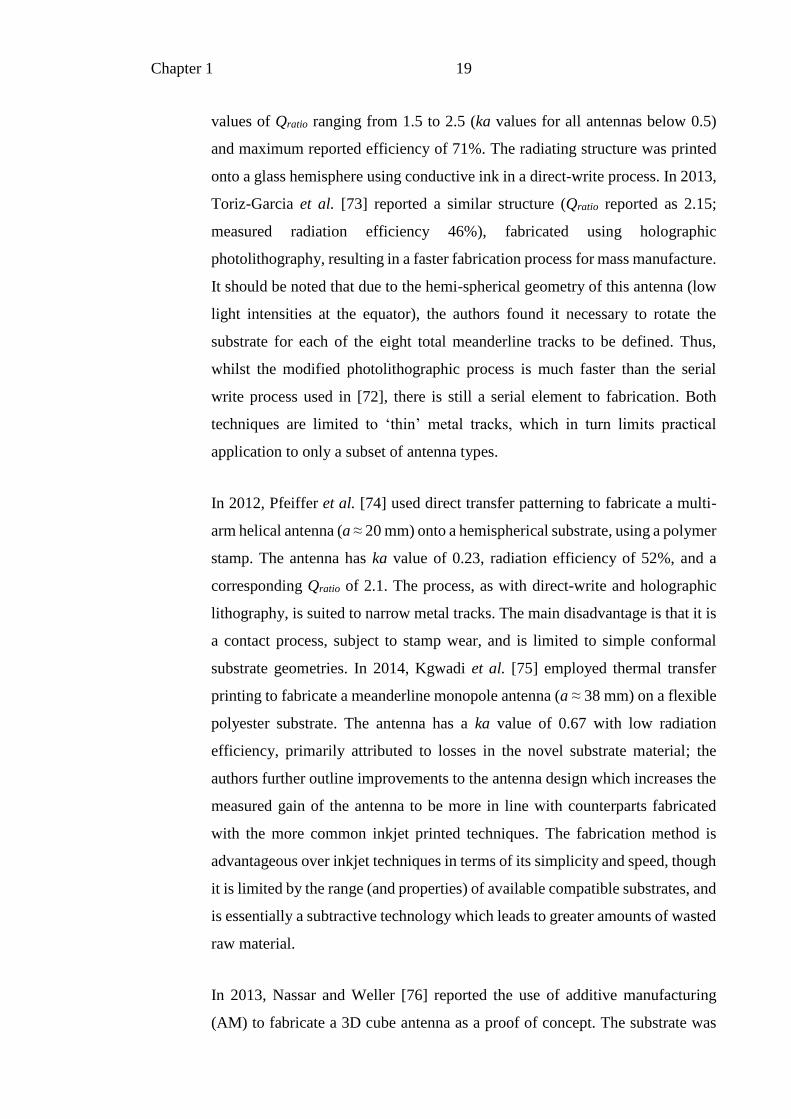
Chapter 1 19
values of Qratio ranging from 1.5 to 2.5 (ka values for all antennas below 0.5)
and maximum reported efficiency of 71%. The radiating structure was printed
onto a glass hemisphere using conductive ink in a direct-write process. In 2013,
Toriz-Garcia et al. [73] reported a similar structure (Qratio reported as 2.15;
measured radiation efficiency 46%), fabricated using holographic
photolithography, resulting in a faster fabrication process for mass manufacture.
It should be noted that due to the hemi-spherical geometry of this antenna (low
light intensities at the equator), the authors found it necessary to rotate the
substrate for each of the eight total meanderline tracks to be defined. Thus,
whilst the modified photolithographic process is much faster than the serial
write process used in [72], there is still a serial element to fabrication. Both
techniques are limited to ‘thin’ metal tracks, which in turn limits practical
application to only a subset of antenna types.
In 2012, Pfeiffer et al. [74] used direct transfer patterning to fabricate a multi-
arm helical antenna (a ≈ 20 mm) onto a hemispherical substrate, using a polymer
stamp. The antenna has ka value of 0.23, radiation efficiency of 52%, and a
corresponding Qratio of 2.1. The process, as with direct-write and holographic
lithography, is suited to narrow metal tracks. The main disadvantage is that it is
a contact process, subject to stamp wear, and is limited to simple conformal
substrate geometries. In 2014, Kgwadi et al. [75] employed thermal transfer
printing to fabricate a meanderline monopole antenna (a ≈ 38 mm) on a flexible
polyester substrate. The antenna has a ka value of 0.67 with low radiation
efficiency, primarily attributed to losses in the novel substrate material; the
authors further outline improvements to the antenna design which increases the
measured gain of the antenna to be more in line with counterparts fabricated
with the more common inkjet printed techniques. The fabrication method is
advantageous over inkjet techniques in terms of its simplicity and speed, though
it is limited by the range (and properties) of available compatible substrates, and
is essentially a subtractive technology which leads to greater amounts of wasted
raw material.
In 2013, Nassar and Weller [76] reported the use of additive manufacturing
(AM) to fabricate a 3D cube antenna as a proof of concept. The substrate was
Chapter 1 20
fabricated using stereolithography apparatus (SLA) [24], and subsequently
patterned with conductive ink. In the same year, Kim [77] reported a multi-arm
helical antenna (a ≈ 26 mm), similar to the one presented in [74], where a plastic
support structure was fabricated using AM and subsequently coated with several
layers of copper paint. The antenna has a ka value of 0.40, radiation efficiency
of 80%, and a corresponding Qratio of 2.2. Both examples illustrate the benefits
of AM as a means of rapid prototyping and initial testing of complex antenna
geometries. The metal coating process can be improved and automated by the
nascent Aerosol Jet technology [78, 79], which is able to spray coat metals onto
conformal substrates. Extending the use of AM to outright ‘print’ metallic
structures is another alternative which can lead towards the potential adoption
of the technology for mass manufacture as well as rapid prototyping.
1.4.3. Case Study: From Monopole to Inverted-F Antenna
This case study looks at the evolution of an IFA from a monopole (illustrated in
Figure 1-4), as an early example of an ESA design which combines geometrical
shaping techniques for miniaturization and matching.
A brief summary of the impedance properties of these antennas is provided here;
full discourse can be found in many RF textbooks, such as [22]. The ILA is
Figure 1-4. Illustration of three types of antennas: (left) wire monopole, (top-right)
inverted-L antenna, and (bottom-right) inverted-F antenna.
∼
∼
∼
≈ λ/4
≈ λ/4
≈ λ/4
a
a
a

Chapter 1 21
realized simply by bending the monopole, with the resultant geometry
resembling the letter ‘L’. This serves to reduce the profile (height) of the
antenna; moreover, the horizontal section acts to increase the capacitance to
ground. The addition of the shorted shunt stub results in an IFA (named so
because the resultant geometry resembles the letter ‘F’); this stub acts to
increase the inductance of the antenna (the exact value is determined primarily
by the length and width of this stub). The resulting structure thus has increased
self-capacitance and self-inductance, with the ability to tune these separately for
optimization at a desired frequency. An added benefit of implementing a shunt
stub (as shown) to increase the self-inductance is that the radiation resistance of
the antenna structure is increased. The impedance can be tuned by the relative
positioning of the feed with respect to the shorting pin. Note that the reduction
in ka value is accompanied by a reduction in gain.
The S11 (see Chapter 2; measure of how well antenna is matched to feed – lower
is better, minima gives frequency of resonance) results are provided in Figure
1-5. It can be seen that the IFA has a lower ka value than the monopole, and a
better match to 50 Ω than the ILA. Metal tracks were modelled as infinitely thin,
with a width of 1 mm and total length 25 mm (equal to λ/4 at 3 GHz). All
configurations were modelled separately over a perfect electrical conductor
(PEC) ground plane several times the operating wavelength. Note that in
computing the ka value of the monopole, the parameter a equals 25.0 mm.
However, for the ILA and IFA, a is halved to 12.5 mm, with the chosen
configuration. (Note that for an antenna above a large ground plane, the
parameter a is determined with the inclusion of the ‘image’ of the antenna in the
ground plane.)

Chapter 1 22
1.4.4. Comments
Various miniaturization techniques were covered in the literature review, and
their application to modern antenna design demonstrated through a host of
recently published ESAs. It is important to note that in the design of an antenna,
the desired application (and in turn specific design parameters such as range,
coverage, power consumption, etc.) determine which of these techniques are
employed. For instance, lumped reactive components can be used to easily tune
an antenna to resonance at frequencies lower than their corresponding physical
dimensions would dictate; however, in certain applications, the added losses
might be undesirable, even at the cost of a more complex design process.
Tuneable antennas using active components exemplify novel solutions to the
bandwidth limitations of ESAs, but the added complexity to fabrication is a
potential hindrance to low cost and high-volume production. A small antenna
that requires a large and complex feed network would in fact be as impractical
as a larger design; in this instance, an antenna designer might be willing to
sacrifice performance for a less-than-optimal matching network. Even a well-
designed ESA might require imaginative metamaterials in order to keep a low
overall profile and improved platform tolerance.
Figure 1-5. Simulated S11 for (orange) monopole, (blue) ILA, and (green) IFA. The
repective resonance frequencies (and ka values) are 2.75 GHz (1.4), 3.00 GHz
(0.78), and 3.75 GHz (1.0).
-18
-15
-12
-9
-6
-3
0
1 2 3 4 5
S1
1(d
B)
Frequency (GHz)

Chapter 1 23
The case study provided an illustrative summary of the design and evolution of
the IFA, which is one of the more common antenna types used in modern
electronics due to its compact size and ease of tuning [22]. The following
chapters provide a more in-depth study of geometrical manipulation techniques
applied to such antennas to further lower their resonant frequency and provide
greater control over their input impedance, whilst keeping the maximum
occupied volume constant. Such an approach is favoured over others due to the
simplicity of design, and consequently, fabrication. Limitations are addressed
with the use of advanced, pioneering manufacturing methods – with the
consistent aim of ease of fabrication.
The antenna designs presented in this Thesis were modelled and optimized
using a specialist 3D EM simulation tool: CST Microwave Studio ® (CST
MWS) [80]. Measurements were subsequently conducted to complement the
simulated results, for which one or both of the time and frequency domain
solvers were used. The time domain solver was typically used initially, with a
hexahedral mesh, to efficiently (computationally) obtain the broadband
frequency behaviour of the antenna under consideration. The frequency domain
solver is typically more computationally intensive, and was employed
subsequently, with a tetrahedral mesh, to obtain results over a narrow frequency
range; this setup is especially apt for antennas possessing electrically small
features and/or 3D features, according to the software’s application notes. For
both solvers, the mesh was sequentially refined to obtain results with a suitably
low error threshold; results from both solvers and measurements were used to
settle on a suitable compromise between accuracy and computational intensity.
1.5. Research Objectives
There were two main research objectives set out for this project.
The first, addressing antenna design, was twofold: (i) investigate and implement
novel miniaturization techniques for planar antennas suited to traditional
fabrication techniques, and (ii) investigate and implement techniques for
improving the performance of the realized ESA.

Chapter 1 24
A novel digitated structure was integrated into a compact, circular profile IFA,
and is introduced in Chapter 3. The same principle is abstracted into a simpler
design to provide a more intuitive understanding of the antenna’s behaviour,
presented in Chapter 4.
From the various techniques available for improving ESA performance, dual
mode operation and voluminous expansion were investigated further; these are
reported in Chapter 3 and Chapter 5, respectively.
Following on from this, the second objective was set to investigate suitable and
viable fabrication techniques for the voluminous, 3D antenna variants.
Holographic photolithography was briefly considered, but additive
manufacturing was ultimately chosen for prototyping and further investigation,
with findings reported in Chapter 5.
A further, overarching objective set out for this project was the fabrication and
measurement of any antenna designs put forth for discussion, so as to improve
confidence beyond only simulated predictions.

Chapter 2 25
CHAPTER 2
Theoretical Background for Electrically Small Antennas
This chapter starts with an overview of the performance metrics commonly used
in the analysis of ESAs, and the measurement setup employed for each of them.
The antenna quality factor is also introduced, to tie in with the commonly used
Qratio metric discussed in Chapter 1. This is followed by an introduction to
antenna fabrication techniques, with focus set on photolithography and additive
manufacturing.
2.1. Antenna Performance Metrics
This section provides a primer on relevant ESA performance metrics, and
provides a description of the measurement techniques and setups used for the
data presented in this Thesis.
2.1.1. Radiation Pattern and Gain
The radiation pattern of an antenna is a spatial representation the EM field
generated by the antenna, as characterized by quantities such as radiation
intensity, directivity, realized gain, etc. [22, 26]. An antenna’s radiation pattern
may be represented either graphically or mathematically, and is typically
described in the far-field (where the pattern shape is invariant over distance
from antenna), along a spherical surface around its centre. Figure 2-1 and Figure
2-2 illustrate the directivity patterns of a typical patch antenna (directional
pattern) and a half-wave dipole antenna (omni-directional pattern), respectively.

Chapter 2 26
3D patterns like the ones shown in Figure 2-2 are often split up into two two-
dimensional (2D) principal plane patterns. Typically, these are the E-plane
(containing the electric field vector in the direction of maximum radiation) and
H-plane (containing the magnetic field vector in the direction of maximum
radiation) patterns. For the sake of convenience, the E-plane is further usually
aligned with one of the geometrical principal planes: either azimuthal or
Figure 2-1. CST MWS model and simulated radiation pattern (3D, directivity) of a
typical circular patch antenna, designed for resonance at 3 GHz (ka = 3.7). Color
scheme: red (max) – green – blue (min); max. directivity ≈ 7.5 dBi.
x
y
zθ
φ
Figure 2-2. CST MWS model and simulated radiation pattern (3D, directivity) of a
typical half-wave dipole antenna, designed for resonance at 3 GHz (ka = 1.4). Color
scheme: red (max) – green – blue (min); max. directivity ≈ 2.1 dBi.
x
y
zθ
φ

Chapter 2 27
elevation [22]. Figure 2-3 shows the 2D principal plane patterns in decibels (dB)
and linear scale for a half-wave dipole antenna with the E-plane aligned with
the geometrical x-y plane (elevation), and the H-plane aligned with the
geometrical z-x plane (azimuth). The decibel (dB) system is employed to
accentuate finer details when there are large variances in a quantity; it is a
logarithmic transformation of a linear scale, depending on whether the displayed
quantity is a power or field (voltage) ratio:
𝑣𝑎𝑙𝑢𝑒|𝑑𝐵 = {
10 log10(𝑣𝑎𝑙𝑢𝑒 |𝑙𝑖𝑛𝑒𝑎𝑟, 𝑝𝑜𝑤𝑒𝑟)
020 log10(𝑣𝑎𝑙𝑢𝑒 |𝑙𝑖𝑛𝑒𝑎𝑟, 𝑓𝑖𝑒𝑙𝑑)
Equation 2-1
In reality, it is rare for the E-plane and H-plane to coincide perfectly with the
principal geometrical planes. For the sake of consistency, all subsequent
radiation patterns provided in this Thesis are presented as 2D patterns in the
azimuth (z-x) and elevation (x-y) planes, with magnitudes given in the dB scale;
local coordinates are displayed with each new geometry to aid the reader.
The directivity, D, (in a particular direction) of an antenna is defined as the
radiation intensity of the antenna (in that direction) relative to the radiation
Figure 2-3. Simulated direcitvity in (left) decibels and (right) linear scale, for the
half-wave dipole of Figure 2-2; (orange) azimuth plane, (blue) elevation plane;
max. directivity ≈ 2.1 dBi or 1.6 (linear).
180°
-135°
-90°
-45°
0°
45°
90°
135°
-30
-20
-10
0
10180°
-135°
-90°
-45°
0°
45°
90°
135°
0
0.5
1
1.5
2
Chapter 2 28
intensity of an isotropic† source (uniformly, in all directions) radiating the same
power [22, 26]. In other words, it reveals whether or not the antenna favours
radiation in certain directions over others, and to what extent. Usually quoted
for the direction where radiation intensity is maximum, it can be expressed
mathematically as [22]:
𝐷𝑚𝑎𝑥 =𝑈𝑚𝑎𝑥
𝑈0=
4𝜋𝑈𝑚𝑎𝑥
𝑃𝑟𝑎𝑑
Equation 2-2
where Umax is the maximum radiation intensity (units: W/steradian) of the
antenna, and U0 is the radiation intensity of an isotropic source radiating the
same power. U0 can be expressed in terms of the total power radiated, Prad, as
[22]:
𝑈0 =𝑃𝑟𝑎𝑑
4𝜋
Equation 2-3
Another useful metric for characterizing the behaviour of an antenna is obtained
by considering the antenna’s conductional and dielectric losses. The gain, G,
(in a particular direction) of an antenna is defined as the radiation intensity of
the antenna (in that direction) relative to the radiation intensity of an isotropic
source radiating with the same input (accepted) power [22, 26]. Also typically
quoted for the direction where it is maximum, gain can be expressed
mathematically as [22]:
𝐺𝑚𝑎𝑥 =𝑈𝑚𝑎𝑥
𝑈𝑖=
4𝜋𝑈𝑚𝑎𝑥
𝑃𝑖𝑛
Equation 2-4
† An isotropic source is an ideal point source that radiates energy uniformly in all directions
[22,26]; as seen in the definition of directivity, it serves as a useful reference to practical, real
antennas.
Chapter 2 29
where Ui is the radiation intensity of an isotropic source radiating with the input
(accepted) power, Pin. Ui can be expressed mathematically as:
𝑈𝑖 =𝑃𝑖𝑛
4𝜋
Equation 2-5
Thus, gain is similar to directivity, and takes into account the power accepted
by the antenna rather than simply the power it radiates. Accordingly, the two
can be related by a simple expression [22]:
𝐺 = 𝜂𝑟𝐷
Equation 2-6
where ηr (≤1) is termed the radiation efficiency of the antenna. If the losses due
to impedance mismatch are included, a new metric called realized gain (Gr) is
obtained. It may be expressed in terms of directivity and the impedance
mismatch factor, M (≤1), as [22, 26]:
𝐺𝑟 = 𝜂𝑟𝑀𝐷
Equation 2-7
Gain is typically presented in the dB scale; being a power ratio, the conversion
from linear to dB (using Equation 2-1) is:
𝐺𝑟|𝑑𝐵 = 10 log10(𝐺𝑟)
Equation 2-8
Since the ratio is defined with respect to an isotropic radiator (G = 0 dB, or 1),
gain is often expressed as dBi (dB over isotropic).
In a system of antennas (i.e. at least one transmitting and one receiving), the
polarization of the radiated EM field may be considered, depending on the
application. The polarization of an antenna is essentially the orientation of the
E-field vector which composes the radiated EM field. For maximum power
transfer between two antennas, they should have the same polarization [22];

Chapter 2 30
losses due to polarization mismatch can be reflected in the gain by adding the
polarization mismatch factor, P (≤1), to the right-hand side of Equation 2-7.
Figure 2-4 shows the same data as shown in Figure 2-3, in dB, but separated for
the φ and θ components; for this example, these can also be designated the co-
and cross- polar patterns, respectively. In practice, for linear polarization,
magnitude in the co-polar plane is generally around 20 dB above that in the
cross-polar plane. The relationship between the total gain, in dB, and partial
gains in the φ and θ components, is simply [22]:
𝐺|𝑑𝐵 = 10 log10(𝐺𝜑 + 𝐺𝜃)
Equation 2-9
There are a few different techniques for measuring the gain of an antenna; the
most common of these is the gain transfer method [22]. The technique uses a
standard gain antenna (SGA) as a reference antenna, to which the gain of the
antenna under test (AUT) is related. The gain, GSGA, and polarization (typically
linear) of the SGA are pre-known. Figure 2-5 depicts a typical laboratory setup
for gain measurement, with the transmit and receive antennas placed inside an
anechoic chamber (to minimize wayward radiation and noise). A photograph of
the laboratory setup at the University of Sheffield is shown in Figure 2-6.
Figure 2-4. Simulated direcitvity in decibels for (left) φ component, and (right) θ
component, for the half-wave dipole of Figure 2-2; (orange) azimuth plane, (blue)
elevation plane. Note that average magnitude for φ component is at-least 100 dB
above that for θ component.
180°
-135°
-90°
-45°
0°
45°
90°
135°
-30
-20
-10
0
10180°
-135°
-90°
-45°
0°
45°
90°
135°
-150
-110
-70
-30
10

Chapter 2 31
With the SGA fixed as the transmit antenna, two sets of S21 measurements are
performed on the receive antenna: once for the power received with the AUT,
termed PAUT, and subsequently for power received with an identical SGA,
termed PSGA. For each set of measurements, the geometrical position of the
transmit and receive antennas is fixed, as is the input power. In a two-port vector
Figure 2-5. Setup for S21 measurements using VNA. The transmit and receive
antennas are placed inside an anechoic chamber (absorber covered room walls) and
separated from each other by a far-field separation.
Absorber
Vector Network Analyzer
Transmit, Tx Receive, Rx
far-field separation
1 2
Figure 2-6. Photograph of the laboratory room showing the control circuitry and
anechoic chamber for S21 measurements using Agilent E5071C VNA. NSI 800F-
10 mounting arm (not visible) holds the AUT; a Rhode & Schwartz HF906 horn
antenna is barely visible inside the chamber.
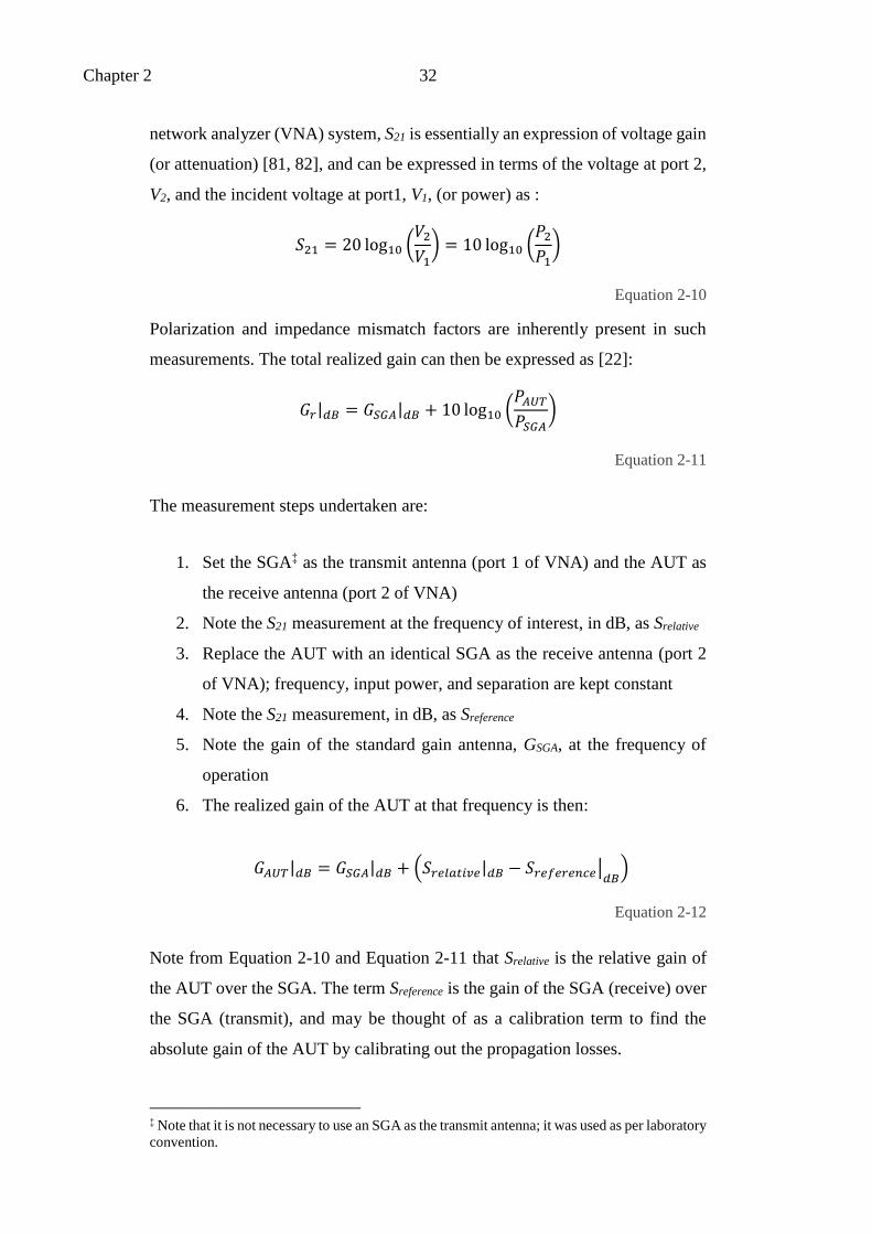
Chapter 2 32
network analyzer (VNA) system, S21 is essentially an expression of voltage gain
(or attenuation) [81, 82], and can be expressed in terms of the voltage at port 2,
V2, and the incident voltage at port1, V1, (or power) as :
𝑆21 = 20 log10 (𝑉2
𝑉1) = 10 log10 (
𝑃2
𝑃1)
Equation 2-10
Polarization and impedance mismatch factors are inherently present in such
measurements. The total realized gain can then be expressed as [22]:
𝐺𝑟|𝑑𝐵 = 𝐺𝑆𝐺𝐴|𝑑𝐵 + 10 log10 (𝑃𝐴𝑈𝑇
𝑃𝑆𝐺𝐴)
Equation 2-11
The measurement steps undertaken are:
1. Set the SGA‡ as the transmit antenna (port 1 of VNA) and the AUT as
the receive antenna (port 2 of VNA)
2. Note the S21 measurement at the frequency of interest, in dB, as Srelative
3. Replace the AUT with an identical SGA as the receive antenna (port 2
of VNA); frequency, input power, and separation are kept constant
4. Note the S21 measurement, in dB, as Sreference
5. Note the gain of the standard gain antenna, GSGA, at the frequency of
operation
6. The realized gain of the AUT at that frequency is then:
𝐺𝐴𝑈𝑇|𝑑𝐵 = 𝐺𝑆𝐺𝐴|𝑑𝐵 + (𝑆𝑟𝑒𝑙𝑎𝑡𝑖𝑣𝑒|𝑑𝐵 − 𝑆𝑟𝑒𝑓𝑒𝑟𝑒𝑛𝑐𝑒|𝑑𝐵
)
Equation 2-12
Note from Equation 2-10 and Equation 2-11 that Srelative is the relative gain of
the AUT over the SGA. The term Sreference is the gain of the SGA (receive) over
the SGA (transmit), and may be thought of as a calibration term to find the
absolute gain of the AUT by calibrating out the propagation losses.
‡ Note that it is not necessary to use an SGA as the transmit antenna; it was used as per laboratory
convention.
Chapter 2 33
For measurements where the frequencies of interest were above 1 GHz, a Rhode
& Schwartz HF906 horn antenna [83] was used as the transmit and reference
antenna. For frequencies below 1 GHz, no SGA was available, and the same
measurement setup was used to obtain the radiation patterns of the AUT without
peak gain information.
2.1.2. Input Impedance
Antennas being transducers, it is important to establish a metric which quantifies
the coupling between the input signal and the radiated EM fields. Generally
referred to as the matching of the antenna, it may be characterized by several
metrics, including voltage standing wave ratio, return loss, and S11. All of these
depend on the input impedance (impedance at the terminals) of the antenna;
the antenna’s input impedance, ZA, (as a function of frequency) is typically
written in terms of its real and imaginary components as [22]:
𝑍𝐴 = 𝑅𝐴 + 𝑗𝑋𝐴 = (𝑅𝑟𝑎𝑑 + 𝑅𝑙𝑜𝑠𝑠) + 𝑗𝑋𝐴
Equation 2-13
where Rrad is radiation resistance, Rloss is loss resistance (comprising of
conductional and dielectric losses), RA is the total antenna resistance, and XA is
reactance (determined primarily by the self-inductance and self-capacitance
within the antenna structure). Denoting the characteristic impedance of the
transmission line feeding into an antenna as ZTL (note that ZTL is treated as 50 Ω
throughout this Thesis), its normalized input impedance, ZNA, is given by:
𝑍𝑁𝐴 =𝑍𝐴
𝑍𝑇𝐿
Equation 2-14
At the frequency of operation (often resonance), ZNA for an antenna should
ideally equal 1 + 𝑗0, implying the absence of a reactive component, and with
the resistive component of the antenna’s impedance equalling that of the
transmission line. Resonance is defined as the frequency point(s) where the
reactive component of impedance equals zero [22]; an antenna can be made self-
Chapter 2 34
resonant by tuning the feed point inductance, L, and capacitance, C, such that
the total feed point reactance equals zero. This condition can be expressed
mathematically in terms of the capacitive and inductive reactances, XC and XL
respectively, as [19]:
𝑐
With the reactance tuned to zero, there is still the remaining challenge of tuning
the feed point resistance of the antenna to 50 Ω – assuming typical usage in a
50 Ω system. (Note that if the antenna is meant to be incorporated in a system
with a different characteristic impedance, say 10 Ω, then its resistive component
needs to also be 10 Ω for a good match.)
The preceding is an ideal scenario which would result in a impedance mismatch
factor, M, of 1; the relationship between M and impedance is given by [22]:
𝑀 = 1 − |𝑍𝐴 − 𝑍𝑇𝐿
𝑍𝐴 + 𝑍𝑇𝐿|
2
= 1 − |𝛤|2
Equation 2-15
where Γ is termed the voltage reflection coefficient and is the complex ratio of
the reflected signal, Vr, to the incident signal, Vi, at a terminal [22]:
𝛤 =𝑉𝑟
𝑉𝑖
Equation 2-16
The reflections (illustrated in Figure 2-7) occur where a mismatch exists
between the antenna and the transmission line; the ratio of the peak-to-minimum
amplitude of the resulting standing wave is termed the voltage standing wave
ratio (VSWR), which can be expressed in terms of Γ as [22]:
𝑉𝑆𝑊𝑅 =1 + |𝛤|
1 − |𝛤|
Equation 2-17

Chapter 2 35
A similar ratio of the incident to reflected power is termed return loss, RL,
given in the linear scale by [11]:
𝑅𝐿 =𝑃𝑖
𝑃𝑟= (
𝑉𝑖
𝑉𝑟)
2
Equation 2-18
where Pi is the power in the incident signal, and Pr is the power in the reflected
signal. As with directivity and gain, return loss is often presented in the decibel
scale; using Equation 2-18 and Equation 2-1, the expression becomes:
𝑅𝐿|𝑑𝐵 = 10 log10 (𝑃𝑖
𝑃𝑟) = 20 log10 (
𝑉𝑖
𝑉𝑟)
Equation 2-19
Using Equation 2-16 and Equation 2-19, return loss can therefore be represented
as a function of Γ as:
𝑅𝐿|𝑑𝐵 = −20 log10|𝛤|
Equation 2-20
The parameter return loss can also be expressed in terms of the parameter S11,
which is often the parameter measured using a VNA. In a two-port VNA system,
S11 is essentially the voltage reflection coefficient, Γ [81, 82]. Thus, using
Equation 2-20, it may be equated, in the dB scale, to the return loss and the input
impedance of the antenna as:
Figure 2-7. Illustration of incident, Vi, and reflected, Vr, signal at the input terminals
of an antenna connected to a transmission line.
~ZA
ZTL
Vr
Vi
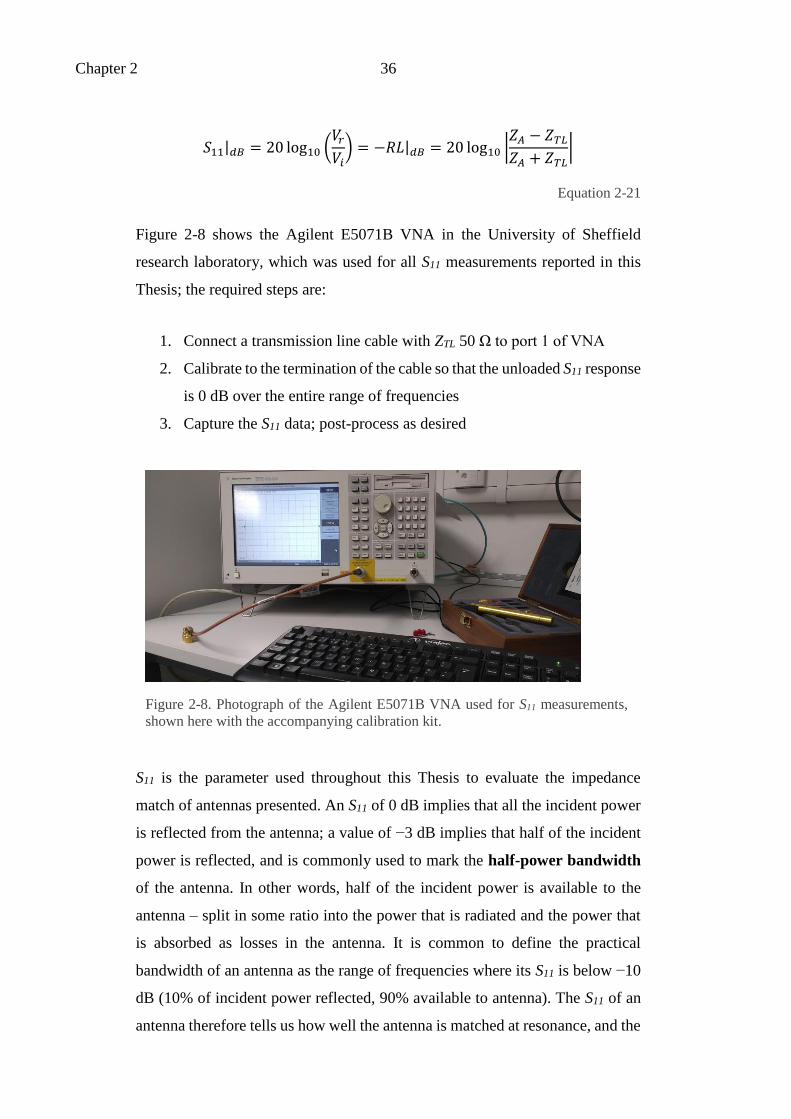
Chapter 2 36
𝑆11|𝑑𝐵 = 20 log10 (𝑉𝑟
𝑉𝑖) = −𝑅𝐿|𝑑𝐵 = 20 log10 |
𝑍𝐴 − 𝑍𝑇𝐿
𝑍𝐴 + 𝑍𝑇𝐿|
Equation 2-21
Figure 2-8 shows the Agilent E5071B VNA in the University of Sheffield
research laboratory, which was used for all S11 measurements reported in this
Thesis; the required steps are:
1. Connect a transmission line cable with ZTL 50 Ω to port 1 of VNA
2. Calibrate to the termination of the cable so that the unloaded S11 response
is 0 dB over the entire range of frequencies
3. Capture the S11 data; post-process as desired
S11 is the parameter used throughout this Thesis to evaluate the impedance
match of antennas presented. An S11 of 0 dB implies that all the incident power
is reflected from the antenna; a value of −3 dB implies that half of the incident
power is reflected, and is commonly used to mark the half-power bandwidth
of the antenna. In other words, half of the incident power is available to the
antenna – split in some ratio into the power that is radiated and the power that
is absorbed as losses in the antenna. It is common to define the practical
bandwidth of an antenna as the range of frequencies where its S11 is below −10
dB (10% of incident power reflected, 90% available to antenna). The S11 of an
antenna therefore tells us how well the antenna is matched at resonance, and the
Figure 2-8. Photograph of the Agilent E5071B VNA used for S11 measurements,
shown here with the accompanying calibration kit.

Chapter 2 37
range of frequencies over which it can be expected to perform up to some pre-
defined standards. Note that other metrics might ultimately influence the
practical bandwidth, including but not limited to gain, polarization, and/or
efficiency.
2.1.3. Radiation Efficiency
The efficiency of an antenna may be characterized by its radiation or total
efficiencies. From Equation 2-6, we observe that the radiation efficiency can be
derived from the gain and directivity of the antenna, if both are available.
Radiation efficiency is defined as the power radiated by an antenna, Prad,
relative to the power accepted by the antenna, Pin, [22, 26] and may be related
to the radiation resistance and loss resistance as :
𝜂𝑟 =𝑃𝑟𝑎𝑑
𝑃𝑖𝑛=
𝑃𝑟𝑎𝑑
𝑃𝑟𝑎𝑑 + 𝑃𝑙𝑜𝑠𝑠=
𝑅𝑟𝑎𝑑
𝑅𝑟𝑎𝑑 + 𝑅𝑙𝑜𝑠𝑠=
𝑅𝑟𝑎𝑑
𝑅𝐴
Equation 2-22
If the losses due to impedance mismatch are considered, the realized radiation
efficiency (or total efficiency) of the antenna is obtained, and is a useful
practical metric for assessing the performance of an antenna in a system.
A common measurement method employs the use of a Wheeler cap [28] to
separate the Rrad and Rloss terms to subsequently compute the efficiency.
Theoretically, a PEC in the shape of a sphere and the electrical size of one
radiansphere would prevent any radiation from the antenna, whilst not
disturbing the antenna’s near-field [84, 85]. In practice, the geometry may be
different, for instance a cuboid, and the size is non-critical as long as radiation
is prevented and near-fields left undisturbed [11].
Using the constant-loss-resistor method [86], reflectivity (or S11) measurements
easily obtained from a VNA can be used to obtain the Rloss and RA terms required
to compute efficiency. The technique works for resonant antennas (i.e. ideally
no reactive component), with the key assumption that Rloss remains constant

Chapter 2 38
with and without the Wheeler cap encasing the AUT. An equivalent circuit
model showing only the resistive components is shown in Figure 2-9.
The technique is shown to compute the efficiency to satisfactory levels and is
commonly employed for ESA measurements; it is favoured here over other,
more precise techniques due to comparative ease of measurement [11]. Figure
2-10 illustrates a typical measurement setup. With the cap in place, reflecting
all the power radiated by the AUT, Rrad equals zero, leaving only the Rloss term.
The expression for S11(WC) becomes [86]:
𝑆𝑊𝐶 =𝑅𝑙𝑜𝑠𝑠 − 𝑅𝑆
𝑅𝑙𝑜𝑠𝑠 + 𝑅𝑆
Equation 2-23
A subsequent measurement in free space then yields RA. The expression for
S11(FS) is [86]:
𝑆𝐹𝑆 =(𝑅𝑟𝑎𝑑 + 𝑅𝑙𝑜𝑠𝑠) − 𝑅𝑆
(𝑅𝑟𝑎𝑑 + 𝑅𝑙𝑜𝑠𝑠) + 𝑅𝑆
Equation 2-24
Figure 2-9. Equivelent circuit model of an antenna showing source resistance, Rs,
and the loss and radiation resistance terms in antenna.
~
Rloss
Rrad
RS
Pr
Pi
S11

Chapter 2 39
This method is used to compute radiation efficiency from measurements for all
such data presented in this Thesis. The measurement steps undertaken are:
1. Connect a transmission line cable with ZTL 50 Ω to port 1 of VNA
2. Calibrate to the termination of the cable so that the S11 response is 0 dB
over the entire range of frequencies
3. Place the AUT inside a suitably sized Wheeler cap and note the S11
measurement, in linear scale, as SWC
4. Remove the Wheeler cap and note the free space S11 measurement, in
linear scale, as SFS
5. Manipulating Equation 2-23 and Equation 2-24 to obtain expressions for
Rrad and Rloss, the radiation efficiency is given by:
𝜂𝑟 = 1 −(1 − 𝑆𝐹𝑆)(1 + 𝑆𝑊𝐶)
(1 + 𝑆𝐹𝑆)(1 − 𝑆𝑊𝐶)
Equation 2-25
Figure 2-10. S11 measurement setup with (left) Wheeler cap on, and (right) in free
space. Cross-sectional view.
Vector Network Analyzer
1
AUT
≈ λ/2π
Vector Network Analyzer
1
AUT
Wheeler cap free space
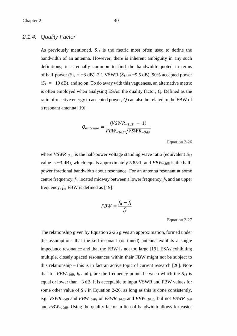
Chapter 2 40
2.1.4. Quality Factor
As previously mentioned, S11 is the metric most often used to define the
bandwidth of an antenna. However, there is inherent ambiguity in any such
definitions; it is equally common to find the bandwidth quoted in terms
of half-power (S11 = −3 dB), 2:1 VSWR (S11 ≈ −9.5 dB), 90% accepted power
(S11 = −10 dB), and so on. To do away with this vagueness, an alternative metric
is often employed when analysing ESAs: the quality factor, Q. Defined as the
ratio of reactive energy to accepted power, Q can also be related to the FBW of
a resonant antenna [19]:
𝑄𝑎𝑛𝑡𝑒𝑛𝑛𝑎 =(𝑉𝑆𝑊𝑅−3𝑑𝐵 − 1)
𝐹𝐵𝑊−3𝑑𝐵√𝑉𝑆𝑊𝑅−3𝑑𝐵
Equation 2-26
where VSWR−3dB is the half-power voltage standing wave ratio (equivalent S11
value is −3 dB), which equals approximately 5.85:1, and FBW−3dB is the half-
power fractional bandwidth about resonance. For an antenna resonant at some
centre frequency, fc, located midway between a lower frequency, fl, and an upper
frequency, fh, FBW is defined as [19]:
𝐹𝐵𝑊 =𝑓ℎ − 𝑓𝑙
𝑓𝑐
Equation 2-27
The relationship given by Equation 2-26 gives an approximation, formed under
the assumptions that the self-resonant (or tuned) antenna exhibits a single
impedance resonance and that the FBW is not too large [19]. ESAs exhibiting
multiple, closely spaced resonances within their FBW might not be subject to
this relationship – this is in fact an active topic of current research [26]. Note
that for FBW−3dB, fh and fl are the frequency points between which the S11 is
equal or lower than −3 dB. It is acceptable to input VSWR and FBW values for
some other value of S11 in Equation 2-26, as long as this is done consistently,
e.g. VSWR−6dB and FBW−6dB, or VSWR−10dB and FBW−10dB, but not VSWR−6dB
and FBW−10dB. Using the quality factor in lieu of bandwidth allows for easier
Chapter 2 41
comparison between various ESAs, particularly as there are fundamental
limitations on the Q that are dependent on the antenna’s electrical size and
radiation efficiency (see Chapter 1).
2.2. Fabrication Methods
This section provides an overview of common and incipient fabrication methods
for the manufacture of antennas. Limitations of a conventional process
(photolithography) are highlighted in the context of inherently 3D antenna
structures; potential alternative fabrication methods are stated, with emphasis
on AM methods.
2.2.1. Photolithography
Photolithography (optical lithography) is a popular process for the fabrication
of integrated circuits and PCBs, including printed antennas [87]. A generic
outline of the process is presented in Figure 2-11.
For low throughput fabrication, as with research, the first step in a typical
photolithography process is typically to coat the entirety of the substrate’s
surface with metal (via thin film deposition processes such as vacuum
deposition, or direct sputtering [88]; this may be followed by electroplating to
increase the thickness of the metal). Often, this initial step is skipped in favour
of purchasing metallized substrates, for instance copper clad FR4. The next step
is proper alignment of the metallized substrate under a photomask; this may be
either a positive or a negative mask, depending on the type of photoresist used.
Photoresists are classed as either positive tone (soluble in a specialized
developer solution once exposed to light) or negative tone (insoluble in
specialized developer solution once exposed to light). Once the substrate
material is coated with a suitable resist, it is exposed to light (depending on the
tone of the resist, a photomask either allows or blocks light through to the area
of interest). A specialized developer solution (again, dependent on the
photoresist used) is then used to remove any excess resist that remains. The
result is a substrate with defined metallic tracks and geometries as per the
required application (e.g. see patch antenna model in Figure 2-1).

Chapter 2 42
It is widely acknowledged that the key to a uniform (profile of) metal coating is
good alignment between the substrate and the photomask. Often, these two need
to be in (near) contact to minimize any diffraction of the light passing through;
diffracted fields would result in uneven exposure and subsequently hinder the
development of the photoresist. As such, a key limitation of traditional
photolithography processes is their unsuitability to non-planar substrate
topologies.
Several solutions have been proposed to overcome this limitation [23, 89-92].
One is the use of conformal photomasks, designed to mate as closely as possible
with the desired non-planar substrate; this approach is very limited in the types
of substrates that can be accommodated, often allowing for only the simplest
non-planar topographies. An alternative is to directly write onto a substrate
Figure 2-11. Illustration of generic photolithography process steps.
Substrate
Photoresist
Metal
(c) Alignment
Photomask
Substrate
Photoresist
Metal
(b) Photoresist coat
Substrate
Metal
(a) Metallization
Substrate
Photoresist
Metal
(d) Exposure
Photomask
Substrate
Metal
(e) Development
Photoresist
Substrate
Metal
(f) Etching
Photoresist
Substrate
Metal
(g) Cleaning

Chapter 2 43
material with conductive ink, or alternatively etch using a laser; these
approaches are, however, limited to a low throughput due to the need to scan
the entirety of the substrate surface in a serial manner. A popular alternative
fabrication method, namely computer numerical control (CNC) machining, is
similarly limited due to its approach of milling away excess metal from
substrates. Whilst modern CNC mills may have multi-axis control, resulting in
the capability of forming complex 3D parts, often the process results in a large
amount of waste (when compared to additive technologies, discussed later).
Another alternative is the use of computer generated holographic (CGH) masks
[23], which allow localized focusing of the optical wave fronts penetrating the
mask. Figure 2-12 illustrates the behaviour of light which has been propagated
through a conventional and a CGH photomask. Holography, in simple terms, is
the process of storing/extracting 3D data in/from a 2D format, using the
principle of interference of (coherent) optical wave fronts [93]. The combination
of holography and photolithography, therefore, allows for the patterning of 3D
substrates.
2.2.2. Additive Manufacture
Additive manufacture, also commonly known as 3D printing, is an umbrella
term given to a range of processes where raw materials are joined up layer by
layer to form objects [24, 94-96]; a distinction is made versus formative (desired
object shape acquired through application of pressure to raw materials, for
instance forging, bending, casting, compaction, etc.) and subtractive (desired
object shape acquired by selective removal of material, for instance milling,
drilling, etching, etc.) manufacturing processes [97].
Figure 2-12. Illustration of the light propagated through a (left) conventional and
(right) CGH photomask. As the distance away from the mask is increased, light
passing through a traditional photomask diffracts, leading to a softening of the
intensity at any particular desired location. CGH masks may be engineered such
that there are multiple, distinct, locallized focal points across the projection area.
Photomask CGH-mask
dis
tan
ce,
z

Chapter 2 44
The numerous technologies classified under AM may be grouped by the raw
materials used (polymers and/or metals), the raw material delivery system
(powder bed, wire feed, etc.), and the heat source (laser, electron beam), among
others; a complete overview of the different technologies may be found in [24].
Through liaison with the Mercury Centre [98] in the University of Sheffield,
powder bed fusion (PBF) processes were trialled to fabricate 3D antenna
geometries. These are one of the earliest commercialized AM processes, and
continue to be one of the most popular [24]. Compared to other AM techniques,
its main advantages are low cost (due in part to its popularity and widespread
adoption), and versatility (supports all types of raw materials); the main
disadvantages (comparatively) are higher power consumption and lower build
volumes.
Figure 2-13 gives a generic illustration of a PBF-AM printer. Pre-processing
involves the conversion of a computer-aided design (CAD) model to a
stereolithography (STL) file, which describes the meshed surface of the object
or part. The STL file is subsequently loaded into an AM printer, where the
specifics of build time, resolution, temperature may be adjusted. A rake or a
roller is used to distribute powder from the cartridges onto the work area,
creating a thin (typically 100 µm) layer of powder. The heat source is then
guided to deliver energy to the surface of the powder bed, melting§ and/or
sintering the powder into the desired shape. A new layer of powder is
subsequently deposited onto a lowered powder bed, melted, and the process
repeated to realize the 3D solid object or part. Surrounding powder remains
loose and is often reclaimed to be used towards a future build.
§ Note that in practice, various fusion processes take place simultaneously, as detailed in [24].
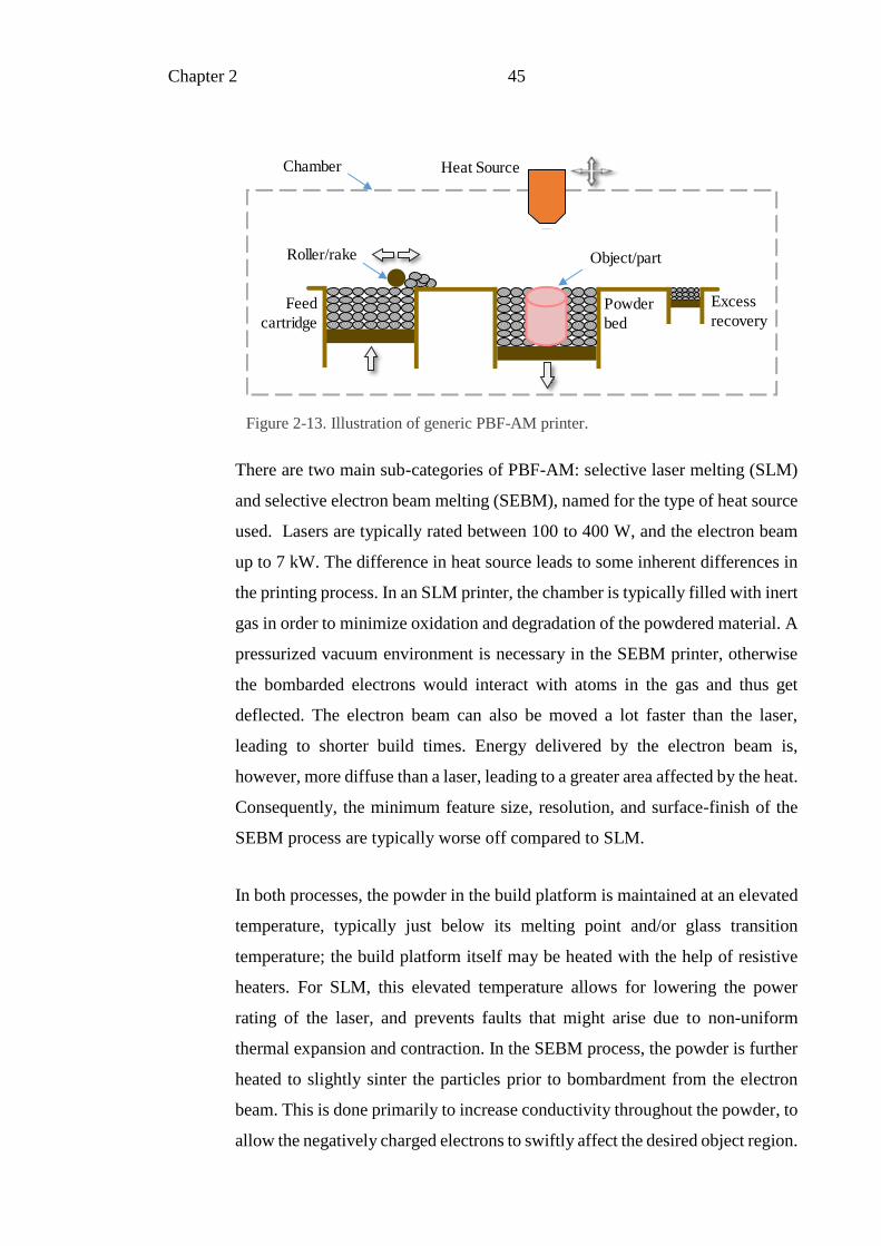
Chapter 2 45
There are two main sub-categories of PBF-AM: selective laser melting (SLM)
and selective electron beam melting (SEBM), named for the type of heat source
used. Lasers are typically rated between 100 to 400 W, and the electron beam
up to 7 kW. The difference in heat source leads to some inherent differences in
the printing process. In an SLM printer, the chamber is typically filled with inert
gas in order to minimize oxidation and degradation of the powdered material. A
pressurized vacuum environment is necessary in the SEBM printer, otherwise
the bombarded electrons would interact with atoms in the gas and thus get
deflected. The electron beam can also be moved a lot faster than the laser,
leading to shorter build times. Energy delivered by the electron beam is,
however, more diffuse than a laser, leading to a greater area affected by the heat.
Consequently, the minimum feature size, resolution, and surface-finish of the
SEBM process are typically worse off compared to SLM.
In both processes, the powder in the build platform is maintained at an elevated
temperature, typically just below its melting point and/or glass transition
temperature; the build platform itself may be heated with the help of resistive
heaters. For SLM, this elevated temperature allows for lowering the power
rating of the laser, and prevents faults that might arise due to non-uniform
thermal expansion and contraction. In the SEBM process, the powder is further
heated to slightly sinter the particles prior to bombardment from the electron
beam. This is done primarily to increase conductivity throughout the powder, to
allow the negatively charged electrons to swiftly affect the desired object region.
Figure 2-13. Illustration of generic PBF-AM printer.
Feed
cartridge
Powder
bed
Roller/rake
Chamber
Object/part
Heat Source
Excess
recovery

Chapter 2 46
This eliminates the need for any sacrificial support structures under overhanging
features, which are sometimes required in SLM printers.
Of the available printers, two were suitable for metallic printing. These were the
laser based Renishaw AM250 [99] and electron beam based Arcam A2 [100].
Plastic support structures were outsourced and printed on machines supplied by
EOS [101] and MakerBot [102].

Chapter 3 47
CHAPTER 3
Miniaturization using Centrally Populated Digitated Structure
In this chapter, a novel contribution to small antenna design is introduced – the
centrally populated digitated structure. The first section compares a
traditional, rectangular IFA (RIFA) with a miniaturized circular IFA (CIFA),
which forms the basis of the antenna profile used throughout this Thesis. This
is followed by the analysis of Inverted-F and planar inverted-F antennas
miniaturized with this technique.
3.1. From a Traditional Inverted-F to a Compact, Circular, Inverted-F Antenna
As previously discussed, practical designs of ESAs must incorporate ways to
miniaturize an antenna (i.e. lower the resonance frequency for fixed overall
dimensions), ensure that conductive and dielectric losses are minimized (reduce
Rloss), and improve the impedance match at resonance (minimize XA and increase
Rrad to 50 Ω). The printed IFA was chosen for further investigation, primarily
due to the ease of manufacture with traditional photolithography techniques, and
in part due to its ubiquity in electronic devices. This section compares a typical,
traditional IFA to a compact, circular profile IFA, which is subsequently
miniaturized and optimized.

Chapter 3 48
3.1.1. Traditional inverted-F antenna design
A traditional RIFA is designed for resonance at 2 GHz; the CAD model consists
of copper (conductivity, σ = 5.8E+7 Sm-1) metallization and lossy FR4 (εr = 4.3,
and loss tangent, tanδ = 0.025) as the substrate. Note that copper and FR4 are
modelled as 35 μm and 0.8 mm thick respectively throughout, unless otherwise
stated. Figure 3-1 shows the front and back of the CAD model. The radius of
the maximum circumscribing sphere, a, is 30 mm. A solder pad is the only
metallization on the back of the antenna; a discrete port is used here to model
the antenna feed. At the point of self-resonance, the antenna has a ka value of
1.26. Note that the total length of the radiating arm and the side length of the
ground plane are approximately equal. The 2 GHz operating frequency was
chosen for practical reasons; antennas operating at higher frequencies would be
too small to easily fabricate or measure, whereas antennas operating at lower
frequencies could not be measured for gain using the HF906 standard gain
antenna (minimum operating frequency 1 GHz) available.
3.1.2. Circular inverted-F antenna design
A compact, circular IFA (CIFA) is realized by truncating the long ground plane
found in traditional designs, and by bending the radiating arm of the antenna in
along a circular arc. The dimensions are chosen so as to achieve self-resonance
Figure 3-1. (left) Front and (right) back view of traditional RIFA designed for
resonance at 2 GHz. All dimensions are given in mm. Via locations labelled with
red dots.
x
y
zθ
φ
23.3
1.0
a
5.4
31.0
5.4
8.8
vias
1.0
9.0
0.7
20.0
0.3
1.5
18.0
vias
vias
24.0
1.0
29.7
vias 1.0
5.4
5.4
5.4
29.7
p
5.4
24.0
q
vias

Chapter 3 49
close to 2 GHz. Note that in order to achieve resonance near 2 GHz, the length
of the curved radiating arm needs to be approximately equal to that of the
radiating arm of the RIFA. Figure 3-2 shows the front and back of the CAD
model; the dimension, a, also the radius of the antenna, is 12 mm. The simulated
antenna is resonant at 2.15 GHz.
3.1.3. Equivalent circuit
Figure 3-3 shows the equivalent circuit model of the antennas discussed above.
The capacitance, C, models the open circuit between the horizontal arm of the
antenna and the ground plane; the inductance, L, models the loop created
between the vertical length of the radiating arm and the short circuit at the
feeding point. The real part of the antenna’s impedance is modelled by the
resistor, R. The overall dimensions of the antenna (specifically the length of the
radiating arm) determine its resonant frequency; the location of the feed point
can be tailored to alter C and L so as to achieve a purely resistive value of the
input impedance.
Figure 3-2. (left) Front and (right) back view of compact CIFA designed for
resonance near 2 GHz. All dimensions are given in mm. Via locations labelled with
red dots.
x
y
zθ
φ
23.3
1.0
a
5.4
31.0
5.4
8.8
vias
1.0
9.0
0.7
20.0
0.3
1.5
18.0
vias
vias
24.0
1.0
29.7
vias 1.0
5.4
5.4
5.4
29.7
p
5.4
24.0
q
vias
Figure 3-3. Equivalent circuit model for the RIFA and CIFA.
~
L R C

Chapter 3 50
3.1.4. Performance comparison
The fabricated antennas are shown in Figure 3-4. The RIFA and CIFA were
both measured to be resonant at 2.10 GHz. In order to examine the effects of the
reduced ground plane and miniaturization, the measured realized gain patterns
are presented in Figure 3-5 (RIFA, φ component), Figure 3-6 (RIFA, θ
component), Figure 3-7 (CIFA, φ component), and Figure 3-8 (CIFA, θ
component), as computed using the gain transfer method. Simulation results are
also provided for comparison. It can be seen that the principal polarization of
both antennas is in the vertical plane (φ component); measured gain for the φ
component is on average slightly over 10 dB higher than for the θ component.
Table 3-1 summarizes the average forward measured gain (±90°) for the two
antennas.
Figure 3-4. Photograph of the fabricated RIFA & CIFA.

Chapter 3 51
Figure 3-5. Realized gain (dBi) for the RIFA at 2.10 GHz; (–––) measured, (– –)
simulated; (orange) azimuth plane, (blue) elevation plane. φ component only.
180°
-135°
-90°
-45°
0°
45°
90°
135°
-35
-25
-15
-5
5
Figure 3-6. Realized gain (dBi) for the RIFA at 2.10 GHz; (–––) measured, (– –)
simulated; (light-orange) azimuth plane, (light-blue) elevation plane. θ component
only.
180°
-135°
-90°
-45°
0°
45°
90°
135°
-75
-55
-35
-15
5

Chapter 3 52
Figure 3-7. Realized gain (dBi) for the CIFA at 2.10 GHz; (–––) measured, (– –)
simulated; (orange) azimuth plane, (blue) elevation plane. φ component only.
180°
-135°
-90°
-45°
0°
45°
90°
135°
-35
-25
-15
-5
5
Figure 3-8. Realized gain (dBi) for the CIFA at 2.10 GHz; (–––) measured, (– –)
simulated; (light-orange) azimuth plane, (light-blue) elevation plane. θ component
only.
180°
-135°
-90°
-45°
0°
45°
90°
135°
-75
-55
-35
-15
5

Chapter 3 53
The combined average forward measured gain (±90°) for the φ component is
−0.97 dBi and −5.22 dBi for the RIFA and CIFA, respectively. In other words,
there is a reduction of approximately 4 dBi in the average forward gain, which
comes with a reduction in the respective ka values from 1.32 to 0.53 (using
measured resonance at 2.10 GHz). For comparison, a recently published CPW-
fed inverted-F antenna achieved a peak gain of 1.4 dBi at its centre frequency
of 2.045 GHz, with a respective ka value of 1.67 [103].
This 4 dBi reduction in gain can alternatively be linked to a reduction in ground
plane area from about 0.04λ2 to 0.01λ2. Whilst not strictly equivalent, a study on
the effects of ground plane sizes of the closely related planar inverted-F antenna
has demonstrated a steady decrease in gain (~ 4.7 dBi to ~ 1.2 dBi; a reduction
of about 3.5 dBi) as the ground plane size was reduced from 2.8λ2 to 0.16λ2,
with no further decrease as the size was reduced from 0.16λ2 to 0.04λ2 [104]. It
should be noted that the precise effects of ground plane on the antenna
performance are complex and are dependent, along with the ground plane size,
on the relative placement of the antenna with respect to the ground plane [105].
To further investigate the performance of the antennas, the radiation efficiency
is computed using the constant-loss-resistor Wheeler cap method. Results are
Table 3-1. Summary of average forward measured gain (±90°) for the RIFA and
CIFA. All values are presented in dBi.
RIFA CIFA
φ
component
θ
component
φ
component
θ
component
Measured
azimuth plane -0.30 -12.65 -4.17 -14.15
Simulated
azimuth plane 0.38 -15.08 -3.49 -24.74
Measured
elevation plane -1.64 -12.12 -6.26 -16.58
Simulated
elevation plane -2.31 -43.97 -4.92 -45.18

Chapter 3 54
shown in Figure 3-9. Measurements were taken with the antennas parallel
(straight connector) and perpendicular (right-angle connector) to the ground
plane of the Wheeler cap. This was done to ensure precision in the
measurements; a high discrepancy would indicate that either the antenna is not
positioned centrally or the cap is too small and causing too much interference
to the near field (a more detailed study on the accuracy and precision of radiation
efficiency measurements can be found in Chapter 4). At their measured resonant
frequency of 2.10 GHz, the RIFA has a maximum radiation efficiency of 88%
and the CIFA of 49% (averaged); note that measurement precision is about ±10
percentage points. Hence, going by measured results, we see a drop of
approximately 39 percentage points in the radiation efficiency as we move from
a traditional IFA design to one that is more compact. For the sake of
completeness, at their respective simulated resonant frequencies, the RIFA
(2.00 GHz) had a simulated radiation efficiency of 92%, while for the CIFA
(2.15 GHz) it was 60%.
Figure 3-9. Measured radiation efficiency for (orange) CIFA, and (blue) RIFA;
(–––) straight connector (– –) right-angle connector. Plotted for ±10 MHz about
resonance frequency.
0
20
40
60
80
100
2.09 2.10 2.11
Rad
iati
on E
ffic
iency
(%
)
Frequency (GHz)

Chapter 3 55
3.2. 2.45 GHz Electrically Small Inverted-F Antenna
Based on the CIFA design presented above, the addition of a centrally populated
digitated structure was proposed. This structure would raise the self-inductance
and self-capacitance of the antenna, allowing for more precise impedance
matching and the added benefit of further reducing the resonant frequency of
the antenna.
3.2.1. Antenna Design – Mini-SMP Connector
An antenna based on this compact design, operating at a desired frequency of
2.4 GHz, was designed and optimized in CST MWS. The antenna was simulated
with copper metallization on a 0.8 mm thick lossy FR4 substrate (εr = 4.3,
tanδ = 0.025). For resonance at 2.4 GHz, the optimized design has a total
diameter of 18 mm. Maintaining the same overall dimensions for a CIFA
resulted in it resonating at 2.8 GHz. Figure 3-10 shows the front view of this
circular, digitated IFA design (CDIFAmSMP), along with the equivalent
CIFAmSMP design having the same overall dimension. The antennas are fed from
the bottom of the substrate, and the excitation of the radiating arm achieved
using through-vias, as shown in Figure 3-10. The digits increase capacitance to
the ground plane, as well as introducing several inductive loops to increase the
antenna’s self-inductance.
Figure 3-10. Front views of the (left) CDIFAmSMP and (right) equivalent CIFAmSMP.
All dimensions are given in mm. Via locations labelled with red dots.
x
y
zθ
φ
23.3
1.0
a
5.4
31.0
5.4
8.8
vias
1.0
9.0
0.7
20.0
0.3
1.5
18.0
vias
vias
24.0
1.0
29.7
vias 1.0
5.4
5.4
5.4
29.7
p
5.4
24.0
q
vias

Chapter 3 56
The small physical size of the antenna necessitated the use of a mini-SMP
(mSMP) connector; to allow for measurements, a custom mSMP–SMA adaptor
was fashioned, as calibration kits for the VNA were only available with SMA
type connections. A photograph of the fabricated CDIFAmSMP is shown in
Figure 3-11. The adaptor shown is 4.5 cm long, and for simulations of the
antenna with feed structure, is modelled as a coaxial cable of the same length.
3.2.2. Results and Discussion – Mini-SMP Connector
Figure 3-12 compares the measured S11 of the CDIFAmSMP with simulated
results. At the measured resonant frequency of 2.36 GHz, the measured
impedance of the antenna is 49.1 – j1.6 (Figure 3-13). The corresponding ka
value for the antenna only is 0.44, and the FBW−3dB equals 10%. Simulation
results are provided for the antenna only model, as well as the model containing
a length of coaxial cable. Of note is the additional loss incurred due to the feed
cable, which has an effect on the magnitude of the return loss, widening the
FBW−3dB; these effects are well documented and something antenna designers
need to be aware of when working with ESAs [11, 106]. For the sake of
completeness, simulation results for the antenna-only model of CIFAmSMP are
also included in Figure 3-12.
Figure 3-11. Photograph of the fabricated CDIFAmSMP mounted on a custom-made
mSMP–SMA adaptor.

Chapter 3 57
The radiation efficiency of the CDIFAmSMP was computed using the constant-
loss-resistor Wheeler cap measurement method [86] (as described in Chapter 2),
using an aluminium box of side length 10 cm; the results are plotted in Figure
3-14. Once again, simulation results are provided for the antenna only model,
as well as the antenna with feed cable. At resonance, the measured radiation
efficiency for the CDIFAmSMP is 70%, though it should be noted that there is a
Figure 3-12. S11 results for the CDIFAmSMP; (orange) measured, (blue) simulated;
(– –) antenna with feed structure, (···) antenna-only simulation; (grey) CIFAmSMP
antenna-only simulation.
-25
-20
-15
-10
-5
0
2.0 2.2 2.4 2.6 2.8 3.0
S1
1(d
B)
Frequency (GHz)
Figure 3-13. Measured input impedance of the CDIFAmSMP; (orange) resistance, R,
and (blue) reactance, jX. Plotted for ±10 MHz around the resonant frequency.
-2
0
2
4
30
40
50
60
2.35 2.36 2.37
Rea
ctan
ce, jX
(Ω
)
Res
ista
nce
, R
(Ω
)
Frequency (GHz)
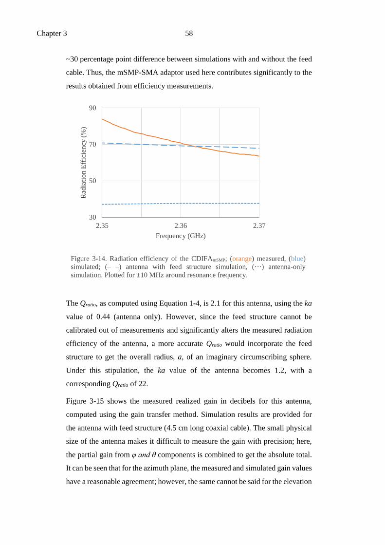
Chapter 3 58
~30 percentage point difference between simulations with and without the feed
cable. Thus, the mSMP-SMA adaptor used here contributes significantly to the
results obtained from efficiency measurements.
The Qratio, as computed using Equation 1-4, is 2.1 for this antenna, using the ka
value of 0.44 (antenna only). However, since the feed structure cannot be
calibrated out of measurements and significantly alters the measured radiation
efficiency of the antenna, a more accurate Qratio would incorporate the feed
structure to get the overall radius, a, of an imaginary circumscribing sphere.
Under this stipulation, the ka value of the antenna becomes 1.2, with a
corresponding Qratio of 22.
Figure 3-15 shows the measured realized gain in decibels for this antenna,
computed using the gain transfer method. Simulation results are provided for
the antenna with feed structure (4.5 cm long coaxial cable). The small physical
size of the antenna makes it difficult to measure the gain with precision; here,
the partial gain from φ and θ components is combined to get the absolute total.
It can be seen that for the azimuth plane, the measured and simulated gain values
have a reasonable agreement; however, the same cannot be said for the elevation
Figure 3-14. Radiation efficiency of the CDIFAmSMP; (orange) measured, (blue)
simulated; (– –) antenna with feed structure simulation, (···) antenna-only
simulation. Plotted for ±10 MHz around resonance frequency.
30
50
70
90
2.35 2.36 2.37
Rad
iati
on
Eff
icie
ncy
(%
)
Frequency (GHz)
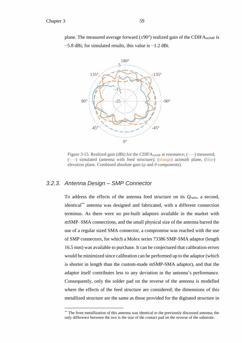
Chapter 3 59
plane. The measured average forward (±90°) realized gain of the CDIFAmSMP is
−5.8 dBi; for simulated results, this value is −1.2 dBi.
3.2.3. Antenna Design – SMP Connector
To address the effects of the antenna feed structure on its Qratio, a second,
identical** antenna was designed and fabricated, with a different connection
terminus. As there were no pre-built adaptors available in the market with
mSMP–SMA connections, and the small physical size of the antenna barred the
use of a regular sized SMA connector, a compromise was reached with the use
of SMP connectors, for which a Molex series 73386 SMP-SMA adaptor (length
16.5 mm) was available to purchase. It can be conjectured that calibration errors
would be minimized since calibration can be performed up to the adaptor (which
is shorter in length than the custom-made mSMP-SMA adaptor), and that the
adaptor itself contributes less to any deviation in the antenna’s performance.
Consequently, only the solder pad on the reverse of the antenna is modelled
where the effects of the feed structure are considered; the dimensions of this
metallized structure are the same as those provided for the digitated structure in
** The front metallization of this antenna was identical to the previously discussed antenna; the
only difference between the two is the size of the contact pad on the reverse of the substrate.
Figure 3-15. Realized gain (dBi) for the CDIFAmSMP at resonance; (–––) measured,
(– –) simulated (antenna with feed structure); (orange) azimuth plane, (blue)
elevation plane. Combined absolute gain (φ and θ components).
180°
-135°
-90°
-45°
0°
45°
90°
135°
-25
-15
-5
5

Chapter 3 60
Figure 3-10; a photograph of the antenna and the SMP-SMA adaptor is shown
in Figure 3-16.
3.2.4. Results and Discussion – SMP Connector
The measured S11 for the CDIFASMP is presented in Figure 3-17. Simulated
results for the CDIFASMP (including solder pad), as well as the previously
presented simulation results for the CDIFAmSMP (i.e. antenna-only), are also
included. The measured antenna, resonant at 2.33 GHz, has a frequency shift of
3% from the optimized design, and a FBW−3dB of 15% (wider bandwidth as a
result of increased losses). At this frequency, the CDIFA has a ka value of 0.44
considering only the antenna, and 0.59 if the Molex SMP-SMA adaptor is
included to obtain the parameter a.
Figure 3-16. Photograph of two fabricated CDIFASMP and Molex series 73386
SMP–SMA adaptor.

Chapter 3 61
The radiation efficiency of the CDIFASMP was computed using the constant-
loss-resistor Wheeler cap method, using a Wheeler cap box of side length 10
cm. The measured results are compared with simulations for the antenna with
SMP solder pad in Figure 3-18; at resonance, the maximum measured radiation
efficiency is 39%. In order to assess the effects of the orientation of the Wheeler
cap with respect to the antenna, measurements were taken for two orientations
of the Wheeler cap boxes (placed in parallel and diamond alignments, with
respect to the ground plate below, see Figure 4-9); there was an average
difference of 3 percentage points between the two readings. Furthermore, it can
be seen that there is good agreement between measured and simulated results;
as in fact there is between the two different simulation models.
Figure 3-17. S11 results for the CDIFASMP; (orange) measured, (blue) simulated;
(– –) antenna with SMP solder pad simulation, (···) antenna-only simulation.
-25
-20
-15
-10
-5
0
2.0 2.2 2.4 2.6 2.8
S1
1(d
B)
Frequency (GHz)

Chapter 3 62
Subsequently, using Equation 1-4, and substituting the ka value of 0.59 (SMP-
SMA adaptor included), the Qratio for the CDIFA is computed to be 5.0
(excluding the adaptor yields a ka value of 0.44 with corresponding Qratio of
2.4).
Figure 3-19 shows the measured realized gain in decibels for this antenna,
computed using the gain transfer method. The small physical size of the antenna
made it difficult to measure the gain with precision; thus, the partial gain from
φ and θ components is combined to get the absolute total (see Chapter 2).
Simulation results provided here include the solder pad on the reverse of the
antenna. The measured average forward gain of the CDIFASMP is −8.2 dBi; for
simulated results, this value is −5.0 dBi. Overall, there is slightly better
agreement between measurements and simulations, as compared to the gain of
the CDIFAmSMP provided in Figure 3-15.
Figure 3-18. Radiation efficiency for the CDIFASMP; (orange) measured, (blue)
simulated; (–––) measurement with Wheeler cap box in parallel alignment, (– · –)
measurement with Wheeler cap box in diamond alignment; (···) simulation for
antenna with SMP solder pad, (– –) simulation for antenna-only. Plotted for ±10
MHz around resonance frequency.
25
30
35
40
45
50
2.32 2.33 2.34
Rad
iati
on
Eff
icie
ncy
(%
)
Frequency (GHz)
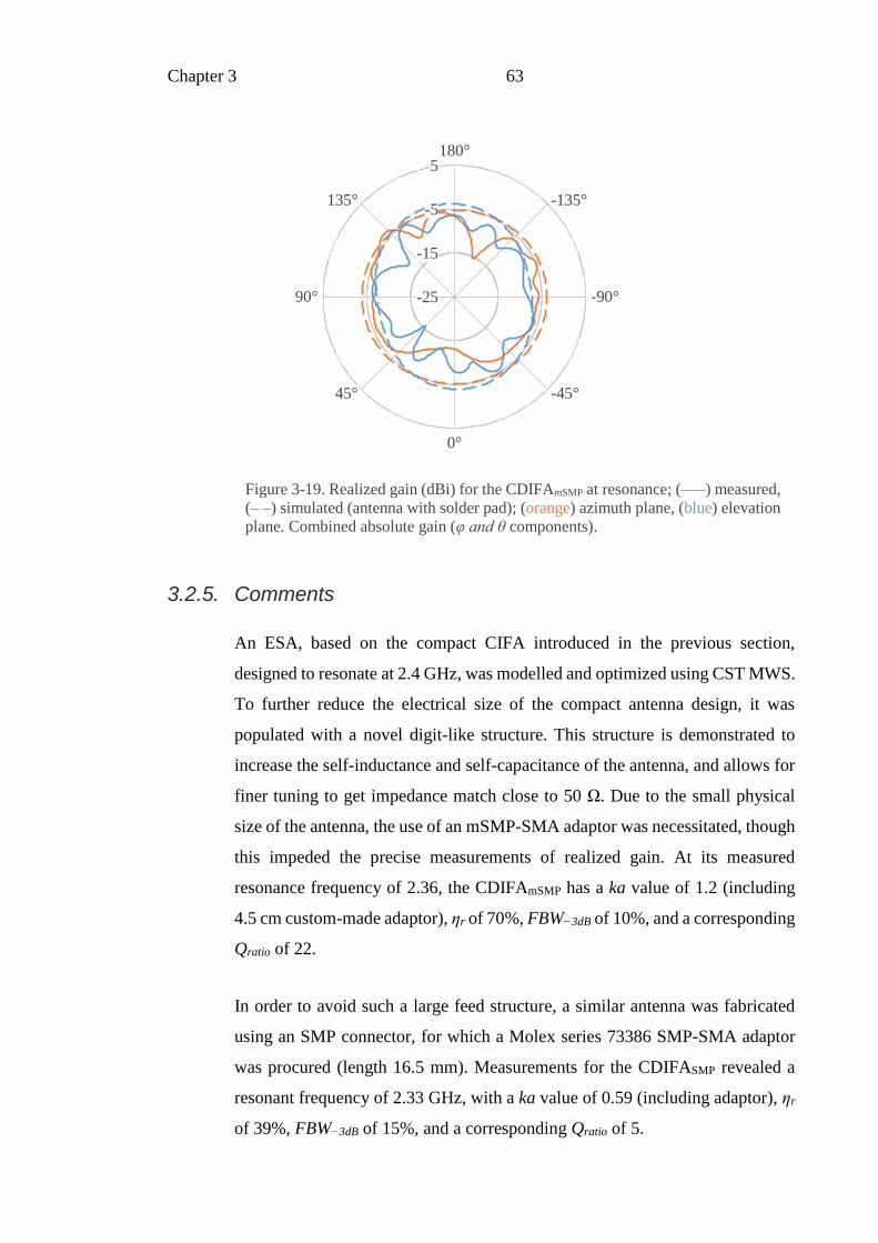
Chapter 3 63
3.2.5. Comments
An ESA, based on the compact CIFA introduced in the previous section,
designed to resonate at 2.4 GHz, was modelled and optimized using CST MWS.
To further reduce the electrical size of the compact antenna design, it was
populated with a novel digit-like structure. This structure is demonstrated to
increase the self-inductance and self-capacitance of the antenna, and allows for
finer tuning to get impedance match close to 50 Ω. Due to the small physical
size of the antenna, the use of an mSMP-SMA adaptor was necessitated, though
this impeded the precise measurements of realized gain. At its measured
resonance frequency of 2.36, the CDIFAmSMP has a ka value of 1.2 (including
4.5 cm custom-made adaptor), ηr of 70%, FBW−3dB of 10%, and a corresponding
Qratio of 22.
In order to avoid such a large feed structure, a similar antenna was fabricated
using an SMP connector, for which a Molex series 73386 SMP-SMA adaptor
was procured (length 16.5 mm). Measurements for the CDIFASMP revealed a
resonant frequency of 2.33 GHz, with a ka value of 0.59 (including adaptor), ηr
of 39%, FBW−3dB of 15%, and a corresponding Qratio of 5.
Figure 3-19. Realized gain (dBi) for the CDIFAmSMP at resonance; (–––) measured,
(– –) simulated (antenna with solder pad); (orange) azimuth plane, (blue) elevation
plane. Combined absolute gain (φ and θ components).
180°
-135°
-90°
-45°
0°
45°
90°
135°
-25
-15
-5
5

Chapter 3 64
Gain pattern measurements were conducted for both the CDIFAmSMP and
CDIFASMP, with neither exhibiting satisfactory agreement with respective
simulations. The difference between simulations and measurements can be
explained by a combination of the following: antenna not level with standard
horn, antenna phase centre not coinciding with centre of rotation of mount,
energy loss in soldered feed connectors, tolerance of substrate material
properties (specifically losses), energy loss due to mSMP-SMA feed structure
or SMP-SMA adaptor. Suggestions for improved measurement results are
provided later as recommendations for future work.
3.3. 530 MHz Dual Resonance Electrically Small Planar Inverted-F Antenna
Bandwidth enhancement for ESAs was investigated with the use of two closely
spaced resonances. Using a similar profile as the CDIFA, along with the
addition of a ground plane on the reverse of the substrate, the antenna can be
fed, as depicted in Figure 3-20, to support two current paths along the edges of
the top metallization. Subsequently, resonances corresponding to the current
paths may be engineered such that they fall close enough together to increase
the effective bandwidth of the antenna. The resulting structure resembles a
variant of the inverted-F antenna – the planar inverted-F antenna. The effects of
a centrally populated digitated structure integrated within this new compact
PIFA were investigated as a means to facilitate miniaturization.

Chapter 3 65
3.3.1. Antenna Design
The circular, digitated, planar inverted-F antenna (CDPIFA) is derived from the
CDIFA of the previous section. Fabrication considerations are the main reason
for the different layout of the digits. Having shorter digits on either side of
copper tracks allows for fewer support structures when building the antenna
using AM (see Chapter 5). The layout is also prefered for holographic
lithography where the negative space between metallizations can be projected
using a computer generated holographic mask; the present structure was found
to optimize faster and with a better contrast ratio when compared to the style of
digits discussed previously.
Figure 3-21 shows the front view of this CDPIFA; the back is completely
metallized and forms the ground plane of this type of antenna. For comparison,
and to facilitate discussion of the optimized design, two variations of a simpler,
circular PIFA design are also included (not to scale). These are termed CPIFA1A
Figure 3-20. Illustration of the current paths on an (top) IFA and (bottom) PIFA.
The ground plane acts to reflect the EM waves born of these currents, and create
the so-called ‘image antenna’.
Ifeed location
shorting pin location
I
feed location
“ground
plane” front
metallization
substrate
front
metallization
“ground
plane”
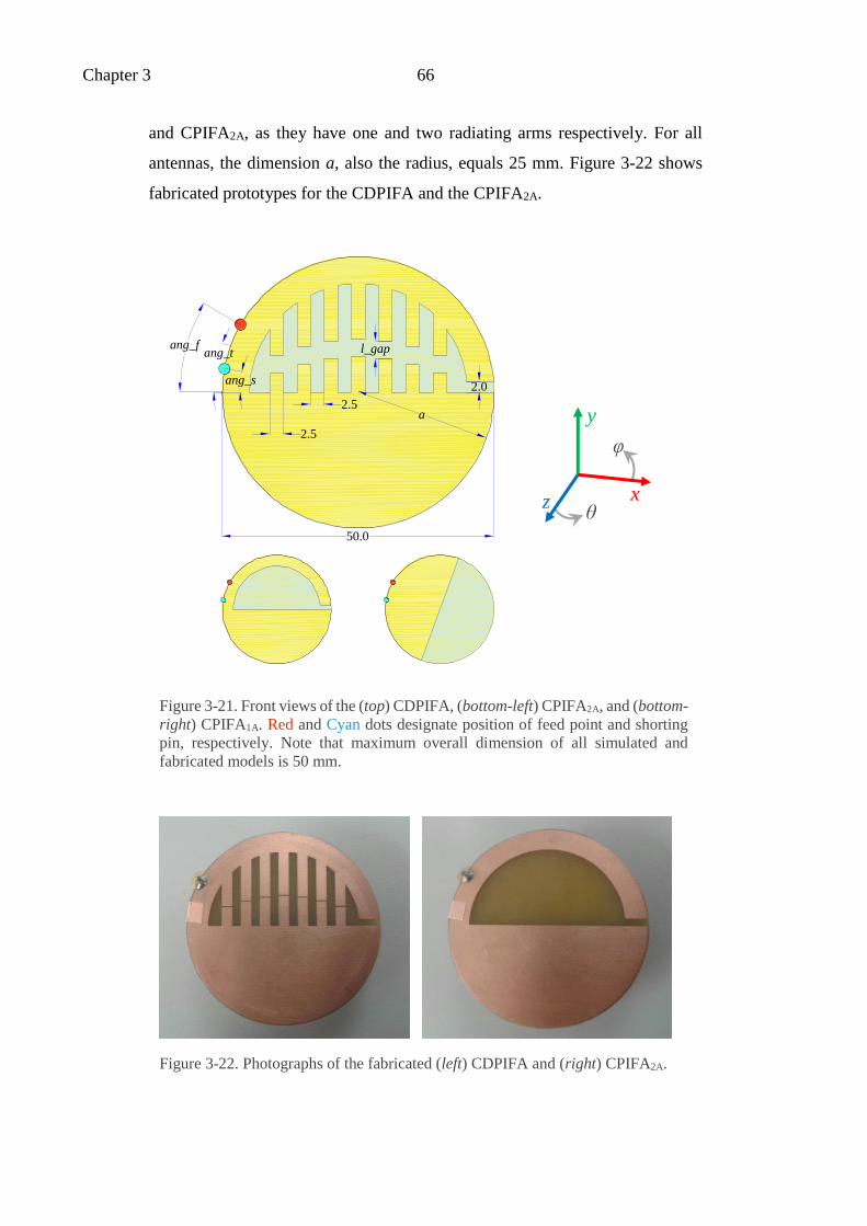
Chapter 3 66
and CPIFA2A, as they have one and two radiating arms respectively. For all
antennas, the dimension a, also the radius, equals 25 mm. Figure 3-22 shows
fabricated prototypes for the CDPIFA and the CPIFA2A.
Figure 3-21. Front views of the (top) CDPIFA, (bottom-left) CPIFA2A, and (bottom-
right) CPIFA1A. Red and Cyan dots designate position of feed point and shorting
pin, respectively. Note that maximum overall dimension of all simulated and
fabricated models is 50 mm.
x
y
zθ
φ
24.0
9.0
0.7
20.0
0.3
1.5
18.0
23.3
1.0
a
5.4
a
29.729.729.7
5.4
5.4p q
24.0
5.4
5.41.0
29.7
31.0
5.4
8.8
50.0
2.0
a
ang_t l_gap
2.5
2.5
ang_s
ang_f
38.1 wtaper
hground
wloop
25.4
strackiloop
ltaper
wtrack
h = 2 mm h = 20 mm h = 30 mm
Figure 3-22. Photographs of the fabricated (left) CDPIFA and (right) CPIFA2A.

Chapter 3 67
3.3.2. Results and Discussion
Figure 3-23 shows the simulated S11 characteristics for the three antennas; where
the parameters of the CDPIFA are as follows: ang_f = 30°, ang_s = 10°, ang_t
= 20°, and l_gap = 0.50 mm. As illustrated, ang_f is the angle in degrees as
measured from the line of azimuth of the antenna to the feed point, ang_s is a
similar angle, but measured up to the shorting pin, ang_t is the angle measured
up to the midway between the feed point and shorting point (when both are
rotated in tandem with relative positions fixed), and finally l_gap is the distance
in millimetres between the top and bottom digits. For simplicity, all other
parameters of the digitated structure are kept constant.
Comparing the plots for CPIFA1A and CPIFA2A, it is evident that dual resonance
behaviour is established with the addition of a second radiating arm to the
antenna. Moreover, the S11 plot for the CDPIFA exhibits two resonances close
together around 540 MHz (with resonances evident at 530 MHz and 550 MHz).
In an application where impedance matching is the primary marker for
bandwidth, such a profile for return loss exhibits a much wider bandwidth than
either of the two resonances of the CPIFA2A. Furthermore, the resonances are
themselves lower down the frequency scale due to the miniaturization effects
manifested by the centrally populated digits.

Chapter 3 68
Here, a detailed review of the optimization process for the CDPIFA is presented,
using the parameters highlighted in Figure 3-21, in order to examine the
antenna’s return loss behaviour. Parametric results for ang_f, ang_s, ang_t, and
l_gap are provided in Figure 3-24, Figure 3-25, Figure 3-26, and Figure 3-27,
respectively.
Varying the relative position of the shorting pin to the feed point – either by
varying ang_f or ang_s results in changing the inductive loop formed in the
PIFA. Varying the gap between the digits in l_gap results in changing the added
capacitance. These parameters can therefore be altered to fine-tune the
impedance match of the CDPIFA. Moreover, varying the parameter ang_t has
the effect of changing the relative lengths of the available current paths, which
in turn determines the frequency of resonance for the antenna. This parameter
can therefore be tuned to bring the two resonances close together.
Figure 3-23. Simulated S11 for (orange) CDPIFA, (blue) CPIFA2A, and (green)
CPIFA1A.
-18
-15
-12
-9
-6
-3
0
400 500 600 700 800 900 1,000
S1
1(d
B)
Frequency (MHz)

Chapter 3 69
Figure 3-24. Simulated S11 for CDPIFA, parameterised ang_f. Legend shown to the
right, units are degrees (°). Original parameter combination shown in orange.
-18
-15
-12
-9
-6
-3
0
400 500 600 700
S1
1(d
B)
Frequency (MHz)
ang_f = 30
ang_f = 28
ang_f = 29
ang_f = 31
ang_f = 32
Figure 3-25. Simulated S11 for CDPIFA, parameterised ang_s. Legend shown to the
right, units are degrees (°). Original parameter combination shown in orange.
-18
-15
-12
-9
-6
-3
0
400 500 600 700
S1
1(d
B)
Frequency (MHz)
ang_s = 10
ang_s = 08
ang_s = 09
ang_s = 11
ang_s = 12

Chapter 3 70
Figure 3-28 and Figure 3-29 compare the measured S11 characteristics of the
fabricated prototypes shown in Figure 3-22 with simulations. Evidently,
measured and simulated results are in good agreement. The slightly lower
resonances observed for the measured results may be attributed to a slightly
higher relative permittivity of substrate, and/or slight changes in the application
Figure 3-26. Simulated S11 for CDPIFA, parameterised ang_t. Legend shown to the
right, units are degrees (°). Original parameter combination shown in orange.
-18
-15
-12
-9
-6
-3
0
400 500 600 700
S1
1(d
B)
Frequency (MHz)
ang_t = 20
ang_t = 05
ang_t = 10
ang_t = 15
ang_t = 25
Figure 3-27. Simulated S11 for CDPIFA, parameterised l_gap. Legend shown to the
right, units are mm. Original parameter combination shown in orange.
-18
-15
-12
-9
-6
-3
0
400 500 600 700
S1
1(d
B)
Frequency (MHz)
l_gap = 0.50
l_gap = 0.75
l_gap = 1.25
l_gap = 1.75
l_gap = 2.25

Chapter 3 71
of the shorting pins and feed connectors in the prototypes versus the simulated
models. Measurements show that the CDPIFA is resonant at 506 and 544 MHz,
with a FBW−3dB of 13%. For S11 below −3 dB, the antenna’s ka value lies
between 0.26 and 0.29.
Figure 3-28. S11 results for CDPIFA; (orange) measured, (blue) simulated.
-18
-15
-12
-9
-6
-3
0
450 500 550 600 650 700 750
S1
1(d
B)
Frequency (MHz)
Figure 3-29. S11 results for CPIFA2A; (orange) measured, (blue) simulated.
-18
-15
-12
-9
-6
-3
0
450 500 550 600 650 700 750
S1
1(d
B)
Frequency (MHz)
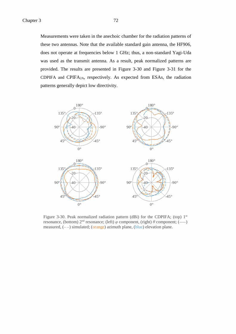
Chapter 3 72
Measurements were taken in the anechoic chamber for the radiation patterns of
these two antennas. Note that the available standard gain antenna, the HF906,
does not operate at frequencies below 1 GHz; thus, a non-standard Yagi-Uda
was used as the transmit antenna. As a result, peak normalized patterns are
provided. The results are presented in Figure 3-30 and Figure 3-31 for the
CDPIFA and CPIFA2A, respectively. As expected from ESAs, the radiation
patterns generally depict low directivity.
Figure 3-30. Peak normalized radiation pattern (dBi) for the CDPIFA; (top) 1st
resonance, (bottom) 2nd resonance; (left) φ component, (right) θ component; (–––)
measured, (– –) simulated; (orange) azimuth plane, (blue) elevation plane.
180°
-135°
-90°
-45°
0°
45°
90°
135°
-40
-20
0180°
-135°
-90°
-45°
0°
45°
90°
135°
-40
-20
0
180°
-135°
-90°
-45°
0°
45°
90°
135°
-40
-20
0180°
-135°
-90°
-45°
0°
45°
90°
135°
-40
-20
0

Chapter 3 73
It can be seen that for either antenna, the θ component is dominant in the first
resonance, and the φ component is dominant in the second. This behaviour can
be seen more clearly in Figure 3-32 and Figure 3-33 for the for the CDPIFA and
CPIFA2A, respectively, where the mean simulated gain is plotted as a function
of frequency. The mean simulated gain for these antennas, with φ and θ
components combined, is given in Table 3-2.
Figure 3-31. Peak normalized radiation pattern (dBi) for the CPIFA2A; (top) 1st
resonance, (bottom) 2nd resonance; (left) φ component, (right) θ component; (–––)
measured, (– –) simulated; (orange) azimuth plane, (blue) elevation plane.
180°
-135°
-90°
-45°
0°
45°
90°
135°
-40
-20
0180°
-135°
-90°
-45°
0°
45°
90°
135°
-40
-20
0
180°
-135°
-90°
-45°
0°
45°
90°
135°
-40
-20
0180°
-135°
-90°
-45°
0°
45°
90°
135°
-40
-20
0

Chapter 3 74
Figure 3-32. Mean* simulated gain for the CDPIFA as a function of frequency;
(purple) φ component, (green) θ component, (red-dashed) combined total.
* mean gain computed from the absolute values over entire range of φ and θ.
-50
-40
-30
-20
-10
400 500 600 700
Gai
n (
dB
i)
Frequency (MHz)
Figure 3-33. Mean* simulated gain for the CPIFA2A as a function of frequency;
(purple) φ component, (green) θ component, (red-dashed) combined total.
* mean gain computed from the absolute values over entire range of φ and θ.
-50
-40
-30
-20
-10
400 500 600 700
Gai
n (
dB
i)
Frequency (MHz)

Chapter 3 75
3.3.3. Comments
The CDPIFA presented and analysed here may be termed an orthogonal-mode,
dual-resonance antenna, i.e. two modes of resonance which are orthogonally
polarized. Thus, it can be utilised to transmit/receive two separate signals at
either resonance, or the same signal with polarization-insensitivity (for example
in applications where circular polarization is tolerated or even purposely
utilized). Improvements to the bandwidth (as determined from the return loss)
are possible by optimizing the structure such that the two resonances operate
close together, which is an advantage over the IFA counterparts. A high
miniaturization factor is achieved, with ka value between 0.26 and 0.29 over the
antennas FBW−3dB of 13%. However, the CDPIFA is a very inefficient antenna,
greatly susceptible to losses in the substrate. This would limit practical
application to only low-bitrate applications, for example, a signalling system on
‘smart’ streetlamps, or IoT enabled devices which have a low on-off time ratio.
Whilst substrate losses can be reduced with the use of more expensive, low-loss
substrates than FR4, this would also deteriorate the match of the antenna at
impedance; further optimization of the antenna design is needed to raise the
radiation resistance at its terminals. Note that the parameter Qratio is not directly
Table 3-2. Comparison of simulated mean gain and radiation efficiency for the
CDPIFA and CPIFA2A.
CDPIFA CPIFA2A
1st
resonance
2nd
resonance
1st
resonance
2nd
resonance
Simulated Resonance
Frequency (MHz) 529 561 572 692
Measured Resonance
Frequency (MHz) 506 544 560 674
Mean* simulated gain
(dBi) -18.4 -16.8 -17.4 -13.5
Simulated Radiation
efficiency (%) 1.6 2.4 2.1 5.3
* mean gain computed from the absolute values over entire range of φ and θ.

Chapter 3 76
applicable to antennas exhibiting two resonances close together, as there is not
yet a consensus within the antenna community regarding whether the
relationships between Q and bandwidth hold for such behaviour [19].
3.4. Summary
This chapter introduced the novel, centrally populated digitated structure,
applied to inverted-F and planar inverted-F antennas. This added structure may
be intuitively likened to additional self-inductance and self-capacitance, a claim
which is explored in greater detail in the following chapter.
First, a traditional, rectangular, IFA was compared to a compact, circular IFA.
Results show that a reduction in ka of 1.32 to 0.53 is achievable at the expense
of realized gain (which drops from 0.97 dBi to −5.22 dBi). A drop in the
radiation efficiency is also observed, with measured values of 88% and 49% for
the RIFA and CIFA, respectively.
Next, the digitated structure was introduced, and the resulting antenna is termed
CDIFASMP. Designed for resonance at 2.4 GHz (measured resonance at
2.33 GHz), the antenna has a ka value of 0.44 (considering only the antenna),
or 0.59 (taking into account the length of the SMP-SMA adaptor used for
measurements). At this frequency, the radiating metallization has a maximum
dimension of 13.6 mm (approximately a tenth of the operational wavelength).
The small physical size of the antenna hampered precise gain and pattern
measurements, though a reasonable similarity between simulations and
measurements can be observed. An alternative metric, in the form of radiation
efficiency was subsequently computed using the constant-loss-resistor Wheeler
cap method, and found to be 39%. Using the measured FBW−3dB of 15%, and
substituting these values into Equation 1-4, the Qratio of this antenna is calculated
to be 5.0.
Finally, a planar derivative of the same design, and optimized for dual-
resonance behaviour is presented, termed the CDPIFA. A parameter study is
reported, focusing on optimizing the resonance frequency of two distinct bands

Chapter 3 77
of operation, with one each belonging to a horizontally and vertically polarized
mode. This CDPIFA is shown to be extremely electrically small, with the lowest
ka value at 0.26. However, in its current configuration, the antenna is highly
lossy, and thereby only suited to a limited range of applications.

Chapter 3 78
(This page intentionally left blank.)

Chapter 4 79
CHAPTER 4
Detailed Analysis of Centrally Populated Digitated Structure
In this chapter, an abstraction of the digitated structure is presented. As
described earlier, the digitated structure adds inductance and capacitance to the
antenna. To offer a more intuitive explanation for this behaviour, it can be
hypothesized that a single vertical and horizontal digit each can replace our
more complex digitated structure, at the expense of less precise control over the
input impedance.
4.1. The Simplified Digitated Structure
4.1.1. Circular Digitated Inverted-F Antenna Design
Figure 4-1 shows the front and back of the CAD model of the compact CIFA
with an integrated abstracted digitated structure, termed here the circular,
digitated, inverted-F antenna LC (CDIFALC); the LC term in subscript is
inspired from the symbols for inductance and capacitance. As previously
reported, this additional digitated structure adds inductance and capacitance to
the antenna, which allows for frequency tuning, keeping the overall dimensions
of the antenna constant. For this circular, planar antenna, the dimension a is also
the radius, and equals 12 mm.

Chapter 4 80
Note that the overall dimensions of this antenna are kept identical to the CIFA
from Chapter 3 to allow for direct comparison; in fact, the principle of
miniaturization expanded upon here may be applied at any frequency, within
reason (i.e. substrate effects might vary too much at very high frequencies), as
shown later in this chapter.
4.1.2. Equivalent Circuit
Figure 4-2 shows the equivalent circuit model of the CDIFALC. An additional
series inductor, LV, and a parallel capacitor, CH, are added to the circuit shown
in Figure 3-3 to model the effects of the digitated structure. This implies that
additional capacitance and inductance can be introduced without altering the
overall dimensions of the antenna, or even the relative lengths of the radiating
arm and inductive loop shortening the arm to the ground plane. The remainder
of this chapter details the effects on the antenna’s performance of effectively
varying these LV and CH components.
Figure 4-1. (left) Front and (right) back view of compact CDIFALC, showing the
dimensions p and q which fully describe the simplified digitated structure. All
dimensions are given in mm. Via locations labelled with red dots.
x
y
zθ
φ
23.3
1.0
a
5.4
31.0
5.4
8.8
vias
1.0
9.0
0.7
20.0
0.3
1.5
18.0
vias
vias
24.0
1.0
29.7
vias 1.0
5.4
5.4
5.4
29.7
p
5.4
24.0
q
vias
Figure 4-2. Equivalent circuit model for the CDIFALC. Addition of digitated
structure increases the self-inductance and self-capacitance of the antenna.
~
L R C
CH
LV
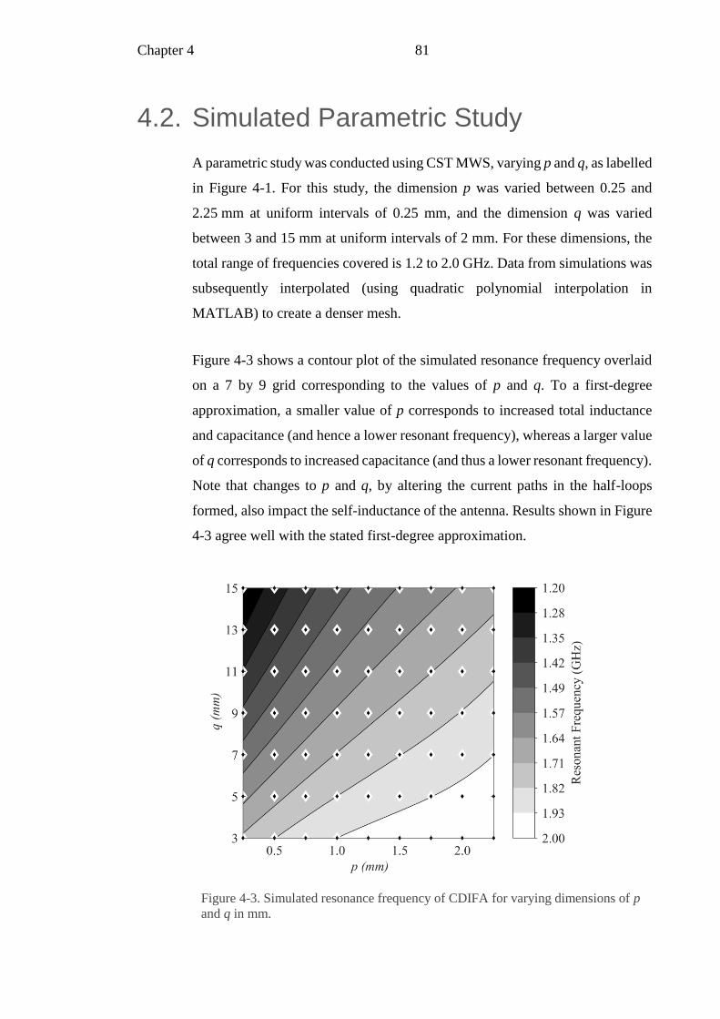
Chapter 4 81
4.2. Simulated Parametric Study
A parametric study was conducted using CST MWS, varying p and q, as labelled
in Figure 4-1. For this study, the dimension p was varied between 0.25 and
2.25 mm at uniform intervals of 0.25 mm, and the dimension q was varied
between 3 and 15 mm at uniform intervals of 2 mm. For these dimensions, the
total range of frequencies covered is 1.2 to 2.0 GHz. Data from simulations was
subsequently interpolated (using quadratic polynomial interpolation in
MATLAB) to create a denser mesh.
Figure 4-3 shows a contour plot of the simulated resonance frequency overlaid
on a 7 by 9 grid corresponding to the values of p and q. To a first-degree
approximation, a smaller value of p corresponds to increased total inductance
and capacitance (and hence a lower resonant frequency), whereas a larger value
of q corresponds to increased capacitance (and thus a lower resonant frequency).
Note that changes to p and q, by altering the current paths in the half-loops
formed, also impact the self-inductance of the antenna. Results shown in Figure
4-3 agree well with the stated first-degree approximation.
Figure 4-3. Simulated resonance frequency of CDIFA for varying dimensions of p
and q in mm.
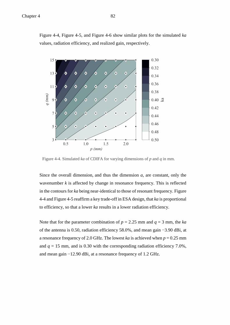
Chapter 4 82
Figure 4-4, Figure 4-5, and Figure 4-6 show similar plots for the simulated ka
values, radiation efficiency, and realized gain, respectively.
Since the overall dimension, and thus the dimension a, are constant, only the
wavenumber k is affected by change in resonance frequency. This is reflected
in the contours for ka being near-identical to those of resonant frequency. Figure
4-4 and Figure 4-5 reaffirm a key trade-off in ESA design, that ka is proportional
to efficiency, so that a lower ka results in a lower radiation efficiency.
Note that for the parameter combination of p = 2.25 mm and q = 3 mm, the ka
of the antenna is 0.50, radiation efficiency 58.0%, and mean gain −3.90 dBi, at
a resonance frequency of 2.0 GHz. The lowest ka is achieved when p = 0.25 mm
and q = 15 mm, and is 0.30 with the corresponding radiation efficiency 7.0%,
and mean gain −12.90 dBi, at a resonance frequency of 1.2 GHz.
Figure 4-4. Simulated ka of CDIFA for varying dimensions of p and q in mm.

Chapter 4 83
These results show clearly the relationship between the dimensions of the
centrally populated digits and the effects on antenna resonance due to the added
Figure 4-5. Simulated radiation efficiency of CDIFA for varying dimensions of p
and q in mm.
Figure 4-6. Simulated mean* realized gain of CDIFA for varying dimensions of p
and q in mm.
* mean gain computed from the absolute values over entire range of φ and θ.
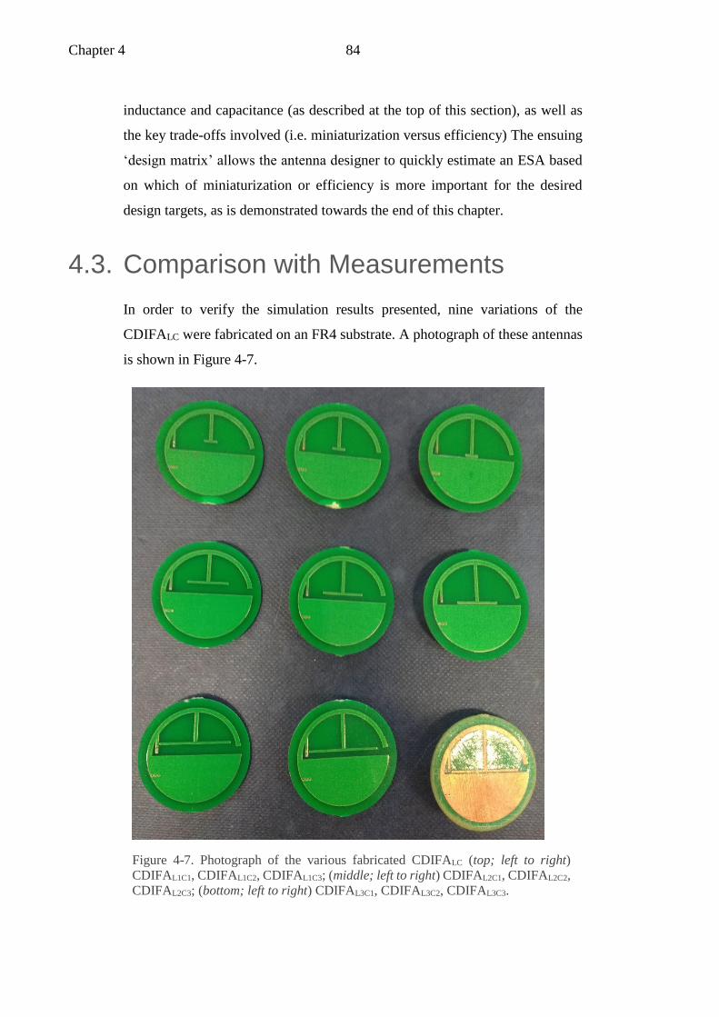
Chapter 4 84
inductance and capacitance (as described at the top of this section), as well as
the key trade-offs involved (i.e. miniaturization versus efficiency) The ensuing
‘design matrix’ allows the antenna designer to quickly estimate an ESA based
on which of miniaturization or efficiency is more important for the desired
design targets, as is demonstrated towards the end of this chapter.
4.3. Comparison with Measurements
In order to verify the simulation results presented, nine variations of the
CDIFALC were fabricated on an FR4 substrate. A photograph of these antennas
is shown in Figure 4-7.
Figure 4-7. Photograph of the various fabricated CDIFALC (top; left to right)
CDIFAL1C1, CDIFAL1C2, CDIFAL1C3; (middle; left to right) CDIFAL2C1, CDIFAL2C2,
CDIFAL2C3; (bottom; left to right) CDIFAL3C1, CDIFAL3C2, CDIFAL3C3.

Chapter 4 85
Measurements were taken for S11, efficiency and realized gain. SMP-SMA
adaptors were fashioned with ferrite sleeves covering semi-rigid coaxial cable.
It was determined from measurements that the ferrite core covering helped
eliminate leakage current on the surface of the semi-rigid cable, as seen from
the convergence of simulations and measurements provided later in this section.
4.3.1. S11 and Fractional Bandwidth
Table 4-1 lists the parameter combinations used for the various CDIFALC, and
compares their measured and simulated resonance frequencies. The FBW−3dB
for the antennas is given in Figure 4-8.
Table 4-1. Parameter combinations and resonant frequencies of the fabricated
CDIFALC.
AUT p (mm) q (mm)
Resonant
frequency
(GHz)
Simulated
Resonant
frequency
(GHz)
Measured
CDIFAL1C1 2.25 3.0 2.00 1.94
CDIFAL1C2 2.25 9.0 1.93 1.88
CDIFAL1C3 2.25 15.0 1.78 1.72
CDIFAL2C1 1.25 3.0 1.88 1.81
CDIFAL2C2 1.25 9.0 1.74 1.68
CDIFAL2C3 1.25 15.0 1.45 1.39
CDIFAL3C1 0.25 3.0 1.73 1.66
CDIFAL3C2 0.25 9.0 1.54 1.49
CDIFAL3C3 0.25 15.0 1.20 1.16

Chapter 4 86
As with simulations, it is observed that an increase in the length of either the
vertical or the horizontal digit results in a lower resonant frequency. On average,
there is a 3.5% frequency shift in the measured resonant frequency compared to
simulated results. As the frequency is consistently shifted down, it is likely an
effect of the material properties of the substrate deviating, within tolerance,
from the quoted value, εr = 4.3. Finally, it can be observed that the FBW−3dB is
reduced as the resonance frequency is lowered, implying an increased Q.
4.3.2. Radiation Efficiency Computation using Wheeler Cap
Radiation efficiency was computed using the constant-loss-resistor Wheeler cap
method. Different sized Wheeler caps were used depending on the resonant
frequency of the AUT, since it is a requirement of the calculation method that
the inner walls of the cap are at-least a diameter (or side length) of λ/π at the
frequency of interest. Measurements were taken for two orientations of the
Wheeler cap boxes (placed in diamond and parallel alignments, with respect to
the ground plate below). Figure 4-9 shows two different Wheeler cap boxes in
these alignments.
Figure 4-8. Range of frequencies where measured S11 ≤ −3 dB for the various
CDIFALC as listed in Table 4-1. Corresponding FBW−3dB is marked as percentage.
9.6 %
9.4 %
8.5 %
9.3 %
8.5 %
6.9 %
8.2 %
7.3 %
5.8 %
CDIFAL1C1
CDIFAL1C2
CDIFAL1C3
CDIFAL2C1
CDIFAL2C2
CDIFAL2C3
CDIFAL3C1
CDIFAL3C2
CDIFAL3C3
1.0 1.2 1.4 1.6 1.8 2.0 2.2
Frequency (GHz)

Chapter 4 87
Efficiency measurements were repeated under various test setups to determine
the precision of the computed results; results are presented here for the
CDIFAL1C1. Figure 4-10 displays the various adaptors used.
First, the CDIFAL1C1 was placed using a straight terminated SMP-SMA adaptor
of length 4 cm (tolerance ±0.4 cm), with the semi-rigid coaxial cable covered in
ferrite sleeves. Measurements were taken for the antenna placed in a 5 cm side
Figure 4-9. Photographs of Wheeler cap measurement setup, (left) side length 10
cm in diamond alignment, (right) side length 5 cm in parallel alignment.
Figure 4-10. Different adaptors used to feed antennas for efficiency measurements:
i) 4 cm bare, ii) 4 cm covered, iii) 4 cm covered, iv) 8 cm bare, v) 8 cm covered.
i)
ii)
iii)
iv)
v)

Chapter 4 88
length box placed in two different alignments (diamond and parallel). The
antenna was resonant at 1.94 GHz; results are presented in Figure 4-11. It can
be seen that the orientation of the Wheeler cap box has negligible effect on the
computed radiation efficiency, indicating that the cap is able to adequately
reflect the radiated fields originating from the antenna. A maximum error of 2
percentage points was obtained using similar measurements conducted for the
other antennas.
Next, measurements for the CDIFAL1C1 were repeated, placing the Wheeler cap
box in parallel alignment with the ground plate, using three different SMP-SMA
adaptors – all with ferrite sleeves covering the length of the coaxial cable. Two
short adaptors of cable length 4 cm and one long adaptor of cable length 8 cm
are used. A box of side length 5 cm was used for the two shorter adaptors, whilst
a box of side length 10 cm was required to accommodate the larger adaptor. For
all three adaptors, the antenna was resonant at 1.94 GHz; results are presented
in Figure 4-12. The computed radiation efficiency at resonance is 56%, 54%,
and 47%, respectively (maximum difference 9 percentage points); similar
measurements were repeated for other antennas with the maximum error
standing at 10 percentage points.
Figure 4-11. Measured radiation efficiency for the CDIFAL1C1, using 4 cm adaptor;
(orange) box parallel aligned, (blue) box diamond aligned. Plotted for ±10 MHz
around resonance frequency.
20
30
40
50
60
70
1.93 1.94 1.95
Rad
iati
on E
ffic
ien
cy (
%)
Frequency (GHz)

Chapter 4 89
Next, measurements for the CDIFAL1C1 were repeated using a 4 cm and 8 cm
adaptor, both without the ferrite sleeve covering. The resonance frequency of
the antenna was 1.97 GHz and 1.92 GHz, respectively; results are presented in
Figure 4-13, along with the results computed using a 4 cm ferrite covered
adaptor for comparison. The computed value of radiation efficiency is 88% and
82% for the 4 cm and 8 cm bare adaptors, respectively.
Figure 4-14 shows the simulated radiation efficiency and corresponding
resonance frequency for the CDIFAL1C1 using a bare coaxial cable to model the
adaptors without ferrite sleeves; the variation in efficiency and resonant
frequency over cable length is obvious. It can be seen that for a cable length of
4 cm, radiation efficiency is 84% (at corresponding resonance frequency of 1.95
GHz), and for a cable length of 8 cm, radiation efficiency is 70% (at
corresponding resonance frequency of 2.00 GHz). Moreover, using a coaxial
cable of length 0.2 cm, the simulated radiation efficiency is 51%, at a
corresponding resonance frequency of 2 GHz – this result is much closer to
computed efficiency values computed with SMP-SMA adaptors where the
coaxial cable is covered with ferrite sleeves, and indeed close to simulated
results where only the solder pad is modelled on the reverse of the antenna.
Figure 4-12. Measured radiation efficiency for the CDIFAL1C1; (orange) 4 cm
adaptor, (blue) other 4 cm adaptor, (green) 8 cm adaptor. Plotted for ±10 MHz
around resonance frequency.
20
30
40
50
60
70
1.93 1.94 1.95
Rad
iati
on
Eff
icie
ncy
(%
)
Frequency (GHz)
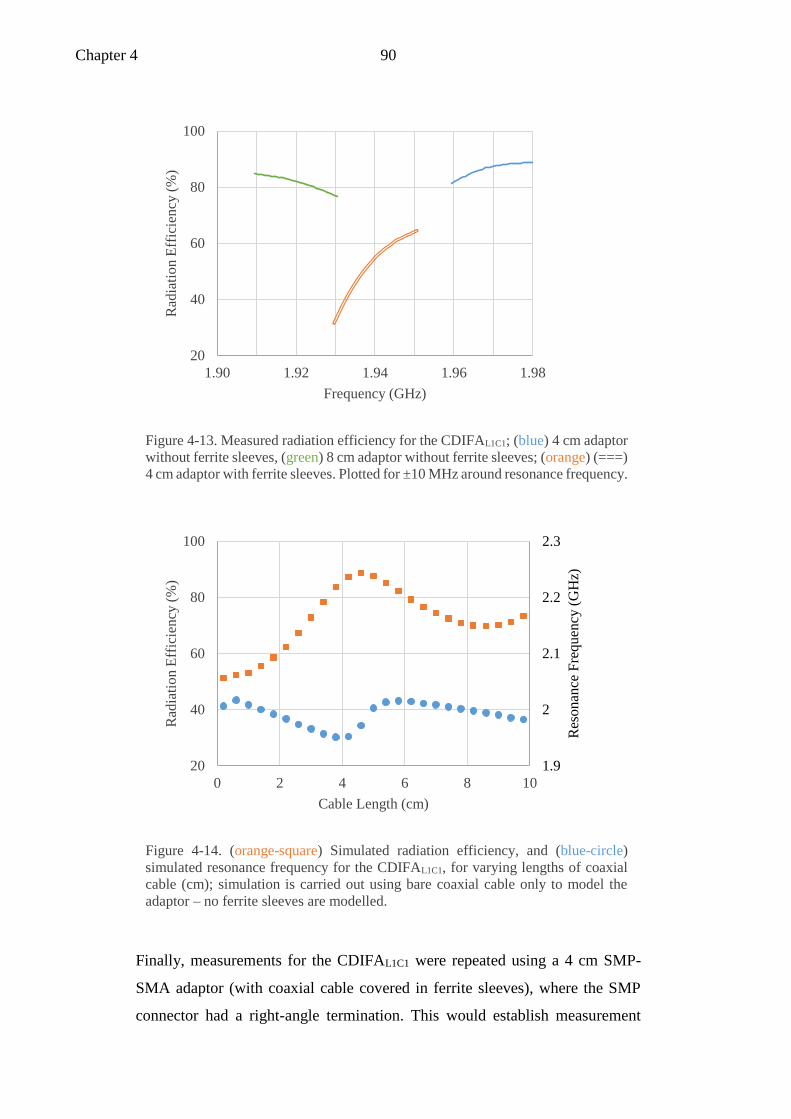
Chapter 4 90
Finally, measurements for the CDIFAL1C1 were repeated using a 4 cm SMP-
SMA adaptor (with coaxial cable covered in ferrite sleeves), where the SMP
connector had a right-angle termination. This would establish measurement
Figure 4-13. Measured radiation efficiency for the CDIFAL1C1; (blue) 4 cm adaptor
without ferrite sleeves, (green) 8 cm adaptor without ferrite sleeves; (orange) (===)
4 cm adaptor with ferrite sleeves. Plotted for ±10 MHz around resonance frequency.
20
40
60
80
100
1.90 1.92 1.94 1.96 1.98
Rad
iati
on
Eff
icie
ncy
(%
)
Frequency (GHz)
Figure 4-14. (orange-square) Simulated radiation efficiency, and (blue-circle)
simulated resonance frequency for the CDIFAL1C1, for varying lengths of coaxial
cable (cm); simulation is carried out using bare coaxial cable only to model the
adaptor – no ferrite sleeves are modelled.
1.9
2
2.1
2.2
2.3
20
40
60
80
100
0 2 4 6 8 10
Res
onan
ce F
requen
cy (
GH
z)
Rad
iati
on E
ffic
iency
(%
)
Cable Length (cm)

Chapter 4 91
precision dependent on the orientation of the AUT. The antenna was resonant
at 1.94 GHz; radiation efficiency results are presented in Figure 4-15, along with
those for the 4 cm straight SMP-SMA adaptor. It can be seen that radiation
efficiency computed using the right-angle terminated adaptor is 54% (deviation
of 2 percentage points from straight terminated adaptor). Similar measurements
for other antennas revealed a maximum error of 6 percentage points between
the efficiency values computed for straight and right-angle terminated adaptors.
With a characterization of the precision for these efficiency measurements,
results were computed for the nine CDIFALC, using the 4 cm straight terminated
SMP-SMA adaptor (with semi-rigid coaxial cable covered in ferrite sleeves),
and with the Wheeler cap placed parallel to the ground plate. Results are listed
in Table 4-2. These results, together with the FBW−3dB results from Figure 4-8,
were substituted into Equation 1-4 to obtain the Qratio of the antennas. Table 4-3
lists the Qratio for each antenna, together with its Q and the corresponding lower
limit. The Qratio for the antennas discussed here ranges from 3.5 to 11.2; as with
the discussion of simulation results above, the bandwidth and efficiency of the
antennas is reduced along with a reduction in their ka values.
Figure 4-15. Measured radiation efficiency for the CDIFAL1C1; (orange) 4 cm
straight terminated adaptor, (blue) 4 cm right-angle terminated adaptor. Plotted for
±10 MHz around resonance frequency.
20
30
40
50
60
70
1.93 1.94 1.95
Rad
iati
on E
ffic
ien
cy (
%)
Frequency (GHz)

Chapter 4 92
4.3.3. Realized Gain and Radiation Patterns
Lastly, results from gain measurements are presented for three selected
antennas, namely the, CDIFAL1C1 (Figure 4-17: φ component; Figure 4-18: θ
Table 4-2. Radiation efficiency, ηr (%) of various AUTs at resonance.
AUT Simulated ηr Measured ηr
CDIFAL1C1 58 56
CDIFAL1C2 53 53
CDIFAL1C3 40 34
CDIFAL2C1 50 49
CDIFAL2C2 38 38
CDIFAL2C3 16 15
CDIFAL3C1 37 35
CDIFAL3C2 22 21
CDIFAL3C3 07 07
Table 4-3. Q, Qlb and Qratio of various AUTs at resonance.
AUT Q Qlb-Chu Qratio
CDIFAL1C1 20.8 6.0 3.5
CDIFAL1C2 21.2 6.1 3.5
CDIFAL1C3 23.5 5.0 4.7
CDIFAL2C1 21.6 6.3 3.4
CDIFAL2C2 23.6 5.9 4.0
CDIFAL2C3 28.9 3.9 7.3
CDIFAL3C1 24.6 5.7 4.3
CDIFAL3C2 27.6 4.6 6.1
CDIFAL3C3 34.4 3.1 11.2

Chapter 4 93
component), CDIFAL2C2 (Figure 4-19: φ component; Figure 4-20: θ
component), and CDIFAL3C3 (Figure 4-21: φ component; Figure 4-22: θ
component). The measurements were carried out in an anechoic chamber using
NSI 800F-10 measurement setup with an Agilent E5071B network analyzer;
Figure 4-16 shows an AUT mounted in the chamber. The gain was computed
using the gain transfer method with a Rhode & Schwartz HF906 horn antenna
as the reference.
Measured and simulated results show good agreement, especially in the φ
component; however, measured results for the θ component are consistently
higher than simulated predictions. This is in part due to the sensitivity of the
measurement setup, and in part due to the amplified effects of artefacts in the
measurement of these physically and electrically small antennas. Note in
particular the undulating pattern for the CDIFAL3C3, where external effects are
felt the strongest due to a very small ka value of 0.29. Polarization is typically
not an important consideration for ESAs, due mainly to the nature of
applications they are commonly found in, though detailed polarization
measurements can be identified as an area of continued research.
Figure 4-16. Photograph of AUT mounted on NSI 800F-10 Z-arm inside anechoic
chamber.

Chapter 4 94
Figure 4-17. Realized gain (dBi) for the CDIFAL1C1 at 1.94 GHz; (–––) measured,
(– –) simulated; (orange) azimuth plane, (blue) elevation plane. φ component only.
180°
-135°
-90°
-45°
0°
45°
90°
135°
-35
-25
-15
-5
5
Figure 4-18. Realized gain (dBi) for the CDIFAL1C1 at 1.94 GHz; (–––) measured,
(– –) simulated; (light-orange) azimuth plane, (light-blue) elevation plane. θ
component only.
180°
-135°
-90°
-45°
0°
45°
90°
135°
-75
-55
-35
-15
5

Chapter 4 95
Figure 4-19. Realized gain (dBi) for the CDIFAL2C2 at 1.68 GHz; (–––) measured,
(– –) simulated; (orange) azimuth plane, (blue) elevation plane. φ component only.
180°
-135°
-90°
-45°
0°
45°
90°
135°
-35
-25
-15
-5
5
Figure 4-20. Realized gain (dBi) for the CDIFAL2C2 at 1.68 GHz; (–––) measured,
(– –) simulated; (light-orange) azimuth plane, (light-blue) elevation plane. θ
component only.
180°
-135°
-90°
-45°
0°
45°
90°
135°
-75
-55
-35
-15
5

Chapter 4 96
From the gain patterns, it can be seen that the primary polarization lies in the φ
component; the combined average forward measured gain (±90°) for the φ
component is −6.32 dBi, −5.99 dBi, and −10.08 dBi for the CDIFAL1C1,
CDIFAL2C2, and CDIFAL3C3, respectively. (Note that there is a more pronounced
Figure 4-21. Realized gain (dBi) for the CDIFAL3C3 at 1.16 GHz; (–––) measured,
(– –) simulated; (orange) azimuth plane, (blue) elevation plane. φ component only.
180°
-135°
-90°
-45°
0°
45°
90°
135°
-35
-25
-15
-5
5
Figure 4-22. Realized gain (dBi) for the CDIFAL3C3 at 1.16 GHz; (–––) measured,
(– –) simulated; (light-orange) azimuth plane, (light-blue) elevation plane. θ
component only.
180°
-135°
-90°
-45°
0°
45°
90°
135°
-75
-55
-35
-15
5
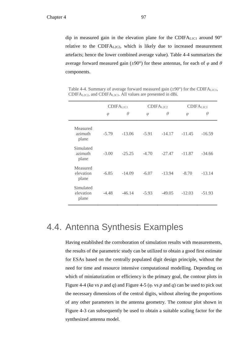
Chapter 4 97
dip in measured gain in the elevation plane for the CDIFAL1C1 around 90°
relative to the CDIFAL2C2, which is likely due to increased measurement
artefacts; hence the lower combined average value). Table 4-4 summarizes the
average forward measured gain (±90°) for these antennas, for each of φ and θ
components.
4.4. Antenna Synthesis Examples
Having established the corroboration of simulation results with measurements,
the results of the parametric study can be utilized to obtain a good first estimate
for ESAs based on the centrally populated digit design principle, without the
need for time and resource intensive computational modelling. Depending on
which of miniaturization or efficiency is the primary goal, the contour plots in
Figure 4-4 (ka vs p and q) and Figure 4-5 (ηr vs p and q) can be used to pick out
the necessary dimensions of the central digits, without altering the proportions
of any other parameters in the antenna geometry. The contour plot shown in
Figure 4-3 can subsequently be used to obtain a suitable scaling factor for the
synthesized antenna model.
Table 4-4. Summary of average forward measured gain (±90°) for the CDIFAL1C1,
CDIFAL2C2, and CDIFAL3C3. All values are presented in dBi.
CDIFAL1C1 CDIFAL2C2 CDIFAL3C3
φ θ φ θ φ θ
Measured
azimuth
plane
-5.79 -13.06 -5.91 -14.17 -11.45 -16.59
Simulated
azimuth
plane
-3.00 -25.25 -4.70 -27.47 -11.87 -34.66
Measured
elevation
plane
-6.85 -14.09 -6.07 -13.94 -8.70 -13.14
Simulated
elevation
plane
-4.48 -46.14 -5.93 -49.05 -12.03 -51.93

Chapter 4 98
To illustrate this design guideline, ESAs based on the geometry of the CDIFALC
are synthesized for operation at 433 MHz (extreme miniaturization), 2.4 GHz
(maximum efficiency), and 5.9 GHz (at least 40% efficiency). Simulated results
for S11 and radiation efficiency are provided in Figure 4-23.
To synthesize an ESA operating at 433 MHz, and with the lowest ka, we pick
out the values of 0.25 mm and 15 mm for p and q respectively, using Figure 4-4,
as these dimensions correspond to the highest degree of miniaturization. Then,
using Figure 4-3, we can see that this antenna would resonate around 1.2 GHz.
Thus, for operation at 433 MHz, the entire antenna is scaled by a factor of 2.8.
To synthesize an ESA operating at 2.4 GHz, and with the highest radiation
efficiency, we pick out the values of 2.25 mm and 3 mm for p and q respectively,
using Figure 4-5, as these dimensions correspond to the highest efficiency.
Then, using Figure 4-3, we can see that this antenna would resonate around 2.0
GHz. Thus, for operation at 2.4 GHz, the entire antenna is scaled by a factor of
0.83.
A number of possible combinations of p and q may be employed to synthesize
an ESA operating at 5.9 GHz with radiation efficiency at least 40%. Assuming
that miniaturization is a secondary aim, we pick out the values of 1.5 mm and 9
mm for p and q respectively, using Figure 4-5, which correspond to
approximately 40% efficiency. Again, using Figure 4-3, we can see that the
resonance frequency of the antenna is approximately 1.8 GHz. Thus, for
operation at 5.9 GHz, the entire antenna is scaled by a factor of 0.30.

Chapter 4 99
4.5. Comparison with selected ESAs from Literature
Figure 4-24 shows a scatter plot of Qratio versus ka for the CDIFASMP (presented
in Chapter 3), and nine variants of the CDIFALC (presented in Chapter 4), along
with selected antennas from the literature review. (For a similar plot with data
points for antennas from the literature review labelled with their respective
reference numbers, see Figure 1-3.) In these terms, it can be seen that the single
resonance antennas presented in this Thesis are comparable to various other
published antennas (which include planar as well as 3D variants). There is a
general trend of increasing Qratio as ka diminishes, which highlights the
difficulty in sustaining comparable performance in ESAs as their electrical size
is reduced. In the figure presented, the only antenna to buck this trend with
measured results is the perfectly spherical 3D wire-grid antenna by Kim [65].
Figure 4-23. Simulated (top) radiation efficiency and (bottom) S11 for the (blue)
CDIFA433MHz, (orange) CDIFA2.4GHz, and (green) CDIFA5.9GHz.
2.3 2.4 2.5
Frequency (GHz)
-25
-20
-15
-10
-5
0
5.8 5.9 6
S1
1(d
B)
Frequency (GHz)
-25
-20
-15
-10
-5
0
0.3 0.4 0.5
S1
1(d
B)
Axis Title
0
20
40
60
80
0.3 0.4 0.5
Radia
tion E
ffic
iency (
%)
Frequency (GHz)
2.3 2.4 2.5
Frequency (GHz)
0
20
40
60
80
5.8 5.9 6
Radia
tion E
ffic
iency (
%)
Frequency (GHz)

Chapter 4 100
From the previous discourse, it is clearly established that measured results for
radiation efficiency line up well with simulation results where only the back
panel is modelled, implying that the SMP-SMA adaptor cables do not need to
be incorporated when computing the ka and subsequently the Qratio for these
antennas. However, it should be noted that the measured results present an
exaggerated FBW, as compared to simulations (computed values show that
simulated FBW-3dB ranges between 50 – 60 % of the measured values, as seen
in Figure 4-25). A likely cause for this increased measured bandwidth is that
while the modified adaptors supress leakage current and thus wayward
radiation, they add some loss to the antenna.
Figure 4-24. Qratio vs ka value scatter plot for CDIFASMP (yellow-square) and
CDIFALC (green-triangle), with selected antennas from literature review for
comparison (c.f. Figure 1-3).
[Chapter 4] [Chapter 3]
[65]
1
10
100
0.1 0.2 0.3 0.4 0.5 0.6 0.7
Qra
tio
ka

Chapter 4 101
Computations taking into account this narrower bandwidth would thus result in
a more accurate depiction of the antenna’s Q. Subsequently, Qratio values are
computed using the simulation results for bandwidth and efficiency, and plotted
in Figure 4-26. As expected, ka values are approximately the same as before,
with an increase in the computed Qratio. Note that the data point for the
CDIFASMP (Chapter 3) incorporates the overall dimension of the antenna
(including the commercially available adaptor used) as well as the increased
bandwidth.
As recommended in the future work section in Chapter 6, the data presented
here may be refined with opto-electric measurement equipment so that only the
antenna itself is the device under test. Additionally, similar antennas may be
designed at a lower resonance frequency to facilitate the use of regular SMA
connectors, such that the calibrated frame of reference for VNA measurements
is moved closer to the actual antenna structure.
Figure 4-25. (–––) Measured and (– –) simulated S11 results for the CDIFAL1C1
(orange), CDIFAL2C2 (blue), CDIFAL3C3 (green).
-36
-30
-24
-18
-12
-6
0
1.0 1.2 1.4 1.6 1.8 2.0 2.2
S1
1(d
B)
Frequency (GHz)

Chapter 4 102
4.6. Summary
This chapter reviewed in detail a new design approach to the optimization of
electrically small antennas. The novel, centrally populated digitated structure
introduced in the previous chapter is abstracted to a simpler structure consisting
of a single vertical and horizontal digit, modelled as an additional series inductor
and parallel capacitor added to the equivalent circuit of a traditional IFA.
A thorough parametric study of the resultant CDIFALC confirms that the key
optimization parameters can be distilled to the lengths of the two digits, which
act as added self-capacitance and self-inductance. The results of the parameter
study produced a ‘design matrix’, which allows the antenna designer to swiftly
decide on the geometrical proportions depending on which of miniaturization
or efficiency is the desired goal at a particular frequency of operation. Thus, a
good first estimate for the digitated IFA can be obtained without the need for
complex computational simulations.
As pointed out earlier, further efficiency and bandwidth gains can be made using
volumetric designs [11, 19, 20]. However, the low profile of planar antennas
Figure 4-26. Qratio vs ka value scatter plot for CDIFALC computed using (green-
triangle) measured and (red-triangle) simulated FBW-3dB and ηr, with selected
antennas from literature review for comparison (c.f. Figure 1-3).
[Chapter 4] [Chapter 3]
[65]
1
10
100
0.1 0.2 0.3 0.4 0.5 0.6 0.7
Qra
tio
ka

Chapter 4 103
translates to high versatility, with narrowband ESAs (such as those discussed in
this chapter) employed in low data rate applications – from the ever-popular
‘smart’ consumer electronics to telemetry uses in industries such as
telecommunications, defence, and healthcare.
Measurement accuracy for the results presented in this section was improved
over previous sections with the use of custom made SMP-SMA adaptors that
comprise a semi-rigid coaxial interconnect surrounded with ferrite loops to
suppress leakage currents. To further alienate the unwanted effects of current-
carrying conductors in the vicinity of the antennas, optical interconnects may be
used (explained in Chapter 6). Finally, a natural continuation of the research
presented thus far, which has focused on antenna design, would be to extend the
design methodology to other types of antennas, such as loops, slots, etc.

Chapter 4 104
(This page intentionally left blank.)

Chapter 5 105
CHAPTER 5
Investigation of Fabrication Techniques
This chapter discusses three types of antennas which were fabricated in-house
as part of an investigation into the prototyping and measurement of inherently
3D antenna designs. For a background on the fabrication processes discussed
here, see Chapter 2.
The first antenna presented is a planar meanderline antenna, fabricated using
photolithography on a glass substrate. The exercise was conducted primarily as
a pre-cursor to holographic photolithography, which was later supplanted with
a greater focus on AM fabrication processes. This was due, in part, to unforeseen
limitations in equipment and personnel during the course of the research, but
primarily due to the opportunity of pioneering measured results for metallic 3D
printed antennas using AM. As such, the next antenna presented is a dome
antenna, based on the design proposed in [72], modified for dual-band
behaviour, and fabricated by ‘damascening’ [107] conductive ink onto a 3D
printed substrate. The substrate is a hemisphere printed out of ABS plastic, with
indented grooves in place of a conductive radiating structure; these grooves
were later filled in with conductive silver paint.
The practical experience gained from these two early ventures was carried
forward into the design, fabrication, and measurement of the planar antennas
presented in preceding chapters as well as the metallic 3D printed antennas
presented in the last section of this chapter. These were fabricated using SEBM
PBF-AM, which is one of the few AM technologies able to directly print metals
[24, 94-96]. Spherical, part-spherical, and flat variants of the same conductor

Chapter 5 106
profile were fabricated to corroborate simulation predictions; measured results
for matching, radiation efficiency, and gain are presented. The metallic
conductors are printed from a titanium alloy, and rested on top of a hollow
plastic substrate printed out of nylon with very thin walls, acting primarily as
support for the metallized structure.
5.1. Meanderline Antenna
As previously mentioned, introducing bends to the radiating arm of a monopole
to achieve a meanderline geometry is useful in reducing the overall electrical
size of the antenna. For the printed monopole variation as discussed here, the
absence of a large ground plane is advantageous in integrated applications
where the availability of space is limited.
5.1.1. Antenna Optimization
A compact, planar meanderline antenna (MLA) was designed on a 1.2 mm thick
glass substrate (εr = 4.8, tanδ = 0.0054) for resonance at 2.45 GHz, with largest
dimension equal to 0.31λ. (The antenna design is based on an MLA on an FR4
dielectric substrate [108].) Glass was chosen as the substrate material since it
can be subjected to processes such as vacuum deposition and withstand
chemical etchants, and may be blown into spherical shapes for experimentation
with holographic photolithography. Figure 5-1 shows the front schematic of the
antenna. The radiating element consists of seven half-turns expanding outwards,
progressing along the y-axis, and is fed by a tapered microstrip line; a partial
ground plane covers the reverse of the substrate.
Table 5-1 lists the optimized parameter values for resonance at 2.45 GHz. The
total track length of the radiating section is 69 mm, fitted inside an area of size
9.6 mm by 36 mm. A gentle taper is used to better match the impedance of the
feed line to that of the radiating section. Considering the total size of the
antenna, the parameter a equals 23 mm; at its simulated resonance frequency of
2.43 GHz, its ka value is 1.2. The antenna is thus on the border of being
categorized as an ESA.
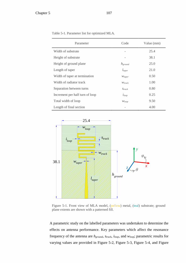
Chapter 5 107
A parametric study on the labelled parameters was undertaken to determine the
effects on antenna performance. Key parameters which affect the resonance
frequency of the antenna are hground, strack, iloop, and wloop; parametric results for
varying values are provided in Figure 5-2, Figure 5-3, Figure 5-4, and Figure
Table 5-1. Parameter list for optimized MLA.
Parameter Code Value (mm)
Width of substrate - 25.4
Height of substrate - 38.1
Height of ground plane hground 25.0
Length of taper ltaper 21.0
Width of taper at termination wtaper 0.50
Width of radiator track wtrack 1.00
Separation between turns strack 0.80
Increment per half turn of loop iloop 0.25
Total width of loop wloop 9.50
Length of final section - 4.00
Figure 5-1. Front view of MLA model, (yellow) metal, (teal) substrate; ground
plane extents are shown with a patterned fill.
x
y
zθ
φ
38.1 wtaper
hground
wloop
25.4
strackiloop
ltaper
wtrack

Chapter 5 108
5-5, respectively. The performance characteristics of the MLA are a function of
the antenna’s current distribution as well as the induced current distribution on
the finite ground plane; thus the size of the ground plane can be varied to achieve
the best possible match at the desired frequency. Other parameters which affect
the resonance frequency vary the overall length of the conductor. The width of
the taper at the feed point and where it meets the radiating structure can be
appropriately adjusted to achieve the best impedance match. The width of the
tracks in the radiating section, keeping all other parameters constant, does not
have a significant effect on the resonance frequency, but affects the input
impedance of the radiating structure.
Figure 5-2. Simulated S11 for MLA, parameterised hground. Legend shown to the
right, units are mm. Original parameter combination shown in orange.
-20
-15
-10
-5
0
1.5 2.0 2.5 3.0 3.5
S1
1(d
B)
Frequency (GHz)
h_ground = 25
h_ground = 22
h_ground = 28

Chapter 5 109
Figure 5-3. Simulated S11 for MLA, parameterised strack. Legend shown to the right,
units are mm. Original parameter combination shown in orange.
-20
-15
-10
-5
0
1.5 2.0 2.5 3.0 3.5
S1
1(d
B)
Frequency (GHz)
s_track = 0.8
s_track = 0.6
s_track = 1.0
Figure 5-4. Simulated S11 for MLA, parameterised iloop. Legend shown to the right,
units are mm. Original parameter combination shown in orange.
-20
-15
-10
-5
0
1.5 2.0 2.5 3.0 3.5
S1
1(d
B)
Frequency (GHz)
i_loop = 0.25
i_loop = 0.00
i_loop = 0.50

Chapter 5 110
5.1.2. Fabrication
The optimized MLA design was fabricated in-house using the photolithographic
fabrication process. For this initial antenna fabrication, a simple negative mask
was used instead of a CGH, as the substrate is planar. A 2 μm coating of Fuji
Photo Film Co. Ltd BPRS200 photoresist was subsequently applied and treated
via exposure to ultraviolet light passed through a negative mask displayed on an
acetate film. After developing the resist, a seed layer (approximately 200 nm
thick in total) of titanium followed by gold was deposited using thermal
evaporation. Subsequently, after etching away excess photoresist (and metal)
using solvents, a copper layer approximately 3-5 μm thick was electroplated
onto this seed metal layer; note that skin depth of copper at 2.4 GHz is 1.3 μm.
The ground plane was fashioned using adhesive copper tape on the reverse of
the substrate. Despite accounting for diffraction effects, actual patterned track
widths were approximately 35% thinner than intended; this was due to low
intensity of light projected at the edges of the defined tracks. Figure 5-6 shows
a photograph of the antenna mounted on a standard SMA connector.
Figure 5-5. Simulated S11 for MLA, parameterised wloop. Legend shown to the right,
units are mm. Original parameter combination shown in orange.
-20
-15
-10
-5
0
1.5 2.0 2.5 3.0 3.5
S1
1(d
B)
Frequency (GHz)
w_loop = 9.5
w_loop = 7.5
w_loop = 11.5

Chapter 5 111
5.1.3. Results and Discussion
Figure 5-7 compares the measured S11 characteristics of the fabricated antenna
with simulated results for optimized parameters, and for all track widths reduced
by 35%. The reduction of the track widths also results in an increase in the
separation between horizontal sections, and therefore meaningfully alters the
antenna performance. Faults in the tracks, especially in the feed line taper are
evident (see Figure 5-6), and are due to improper adhesion of metal on glass;
this is likely due to human errors during the fabrication process, for instance the
introduction of dust on the substrate. Another potential source of error is a sub-
optimal soldered connection between the SMA connector and the antenna. As a
result, the S11 response of the measured MLA is seen to have an abnormal level
of perturbations. At its resonance frequency of 2.2 GHz, the antenna has a ka
value of 1.1; corresponding FBW−3dB and FBW−6dB values are 27% and 13%,
respectively. Note that for the measured S11 response shown in Figure 5-7, the
half-power cut-off is not a reliable measure of fractional bandwidth, whereas
the quarter-power cut-off (FBW−6dB) is more in line with simulation (also
approximately 13%).
Figure 5-6. Photograph of the manufactured MLA, mounted on an SMA connector
(solder not yet applied).

Chapter 5 112
Figure 5-8 shows the measured realized gain in decibels for this antenna,
computed using the gain transfer method. Measured results are only available
for the dominant φ component; simulated results are presented for both φ (co-
polar) and θ (cross-polar) components, and show a difference of more than 20
dB between the two. Measured results for the azimuth plane agree very well
with simulations; in the elevation plane, measured gain is lopsided which is
likely due to the phase centre of the antenna not aligning perfectly with the
centre of rotation of the antenna mount. The average forward gain (±90°) for the
φ component of the MLA is −0.1 dBi (simulation), and −1.8 dBi (measurement).
Figure 5-7. S11 results for the MLA; (orange) measured, (blue) simulated; (– –)
simulation with optimized parameters, (···) simulation with all track widths
reduced by 35%.
-20
-15
-10
-5
0
1.8 2.2 2.6 3.0
S1
1(d
B)
Frequency (MHz)
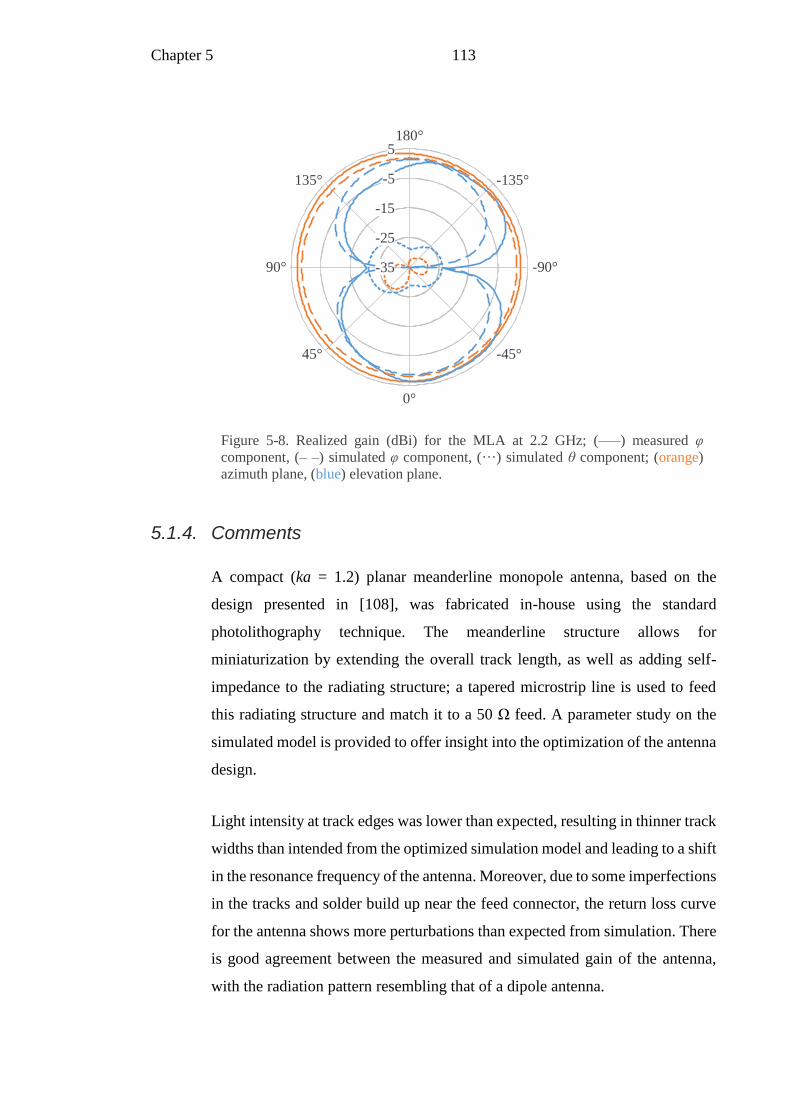
Chapter 5 113
5.1.4. Comments
A compact (ka = 1.2) planar meanderline monopole antenna, based on the
design presented in [108], was fabricated in-house using the standard
photolithography technique. The meanderline structure allows for
miniaturization by extending the overall track length, as well as adding self-
impedance to the radiating structure; a tapered microstrip line is used to feed
this radiating structure and match it to a 50 Ω feed. A parameter study on the
simulated model is provided to offer insight into the optimization of the antenna
design.
Light intensity at track edges was lower than expected, resulting in thinner track
widths than intended from the optimized simulation model and leading to a shift
in the resonance frequency of the antenna. Moreover, due to some imperfections
in the tracks and solder build up near the feed connector, the return loss curve
for the antenna shows more perturbations than expected from simulation. There
is good agreement between the measured and simulated gain of the antenna,
with the radiation pattern resembling that of a dipole antenna.
Figure 5-8. Realized gain (dBi) for the MLA at 2.2 GHz; (–––) measured φ
component, (– –) simulated φ component, (···) simulated θ component; (orange)
azimuth plane, (blue) elevation plane.
180°
-135°
-90°
-45°
0°
45°
90°
135°
-35
-25
-15
-5
5

Chapter 5 114
5.2. Modified Dome Antenna
Based on a previously published antenna design [72, 109], a rapid prototype of
a meanderline hemispherical dome antenna (MHDA) was fabricated on 3D
printed plastic (ABS) and damascened with conductive silver paste to overlay
metal tracks. The work is a precursor to the following section where the
digitated antenna designs discussed earlier are voluminously expanded and
fabricated using 3D printing techniques.
Figure 5-9 shows the CST MWS models of two such antennas. As before, the
elevation plane is the geometrical x-y plane, while the azimuth plane is the
geometrical z-x plane. Both consist of conformal meanderlines on a
hemispherical ABS substrate (εr ≈ 3, tanδ = 0.009) of radius 40 mm. The
antennas are placed on a square FR4 substrate (εr = 4.3,
tanδ = 0.025) of area 16 cm2, with a coaxial feed inserted in the centre for
excitation. The MHDAA consists of eight identical arms (each with a total length
of 425 mm) for even current distribution on the surface of the sphere, and fed
by microstrip feed lines for improved impedance matching. Designed for
closely spaced dual-resonance behaviour, the MHDAB consists of two sets of
four arms each; the longer arms have a length of 520 mm (and are fed by
meandering microstrips), whilst the shorter arms have a length of 260 mm (and
are fed by straight microstrips).
Note that the different geometries were put in place to investigate the effects of
a relative phase delay between the two sets of meanderlines. However, this line
of inquiry was placed out of the scope of the project due to an increased focus
on planar antenna design and the fabrication of the digitated inverted-F based
antennas, as these offered an increased potential for novel research.
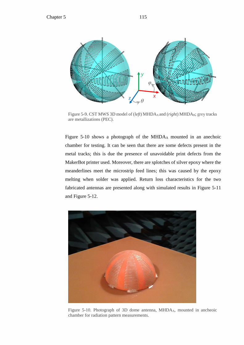
Chapter 5 115
Figure 5-10 shows a photograph of the MHDAA mounted in an anechoic
chamber for testing. It can be seen that there are some defects present in the
metal tracks; this is due the presence of unavoidable print defects from the
MakerBot printer used. Moreover, there are splotches of silver epoxy where the
meanderlines meet the microstrip feed lines; this was caused by the epoxy
melting when solder was applied. Return loss characteristics for the two
fabricated antennas are presented along with simulated results in Figure 5-11
and Figure 5-12.
Figure 5-9. CST MWS 3D model of (left) MHDAA and (right) MHDAB; grey tracks
are metallizations (PEC).
x
y
zθ
φ
Figure 5-10. Photograph of 3D dome antenna, MHDAA, mounted in ancheoic
chamber for radiation pattern measurements.

Chapter 5 116
Measured results for the MHDAA show that the antenna is resonant at the
expected frequency, but that the match is much worse than predicted from
simulations. This is primarily due to the sub-optimal connection between the
microstrip feed lines and the radiating arms. Similarly, for the MHDAB, it can
be seen that whilst the antenna has two distinct measured resonances, the actual
resonance values do not line up well with simulations. The two resonances from
the long and short arms, which were lined up close together to increase
bandwidth at the low frequency point are seen to separate in measurements,
implying that fabricated tracks are not continuous (i.e. shorter current paths);
similar defects along the meanderlines can be seen for the antenna shown in
Figure 5-10. The marked deviation of measured results from simulation
predictions confirmed expectations of poor performance from these antennas
due to various setbacks in the fabrication process, in particular the metal tracks
and connections.
Figure 5-11. S11 for (orange) MHDAA; (–––) measured and (– –) simulated.
-15
-12
-9
-6
-3
0
400 500 600 700 800 900
S1
1(d
B)
Frequency (MHz)

Chapter 5 117
The radiation pattern of the fabricated antennas was measured using a non-
standard Yagi-Uda as the transmit antenna. Therefore, only the peak normalized
radiation patterns are provided.
The MHDAA was measured at its resonance frequency of 670 MHz, and is
shown compared to the pattern at its simulated resonance frequency of 655 MHz
in Figure 5-13. The main polarization is along the θ component. Measurements
and simulations line up well in the azimuth plane, except for a dip around ±110°
present in simulation but absent from measurements; the measured pattern in
the elevation plane is consistently larger than the simulation counterpart. This
deviation is most likely a result of misalignment: the results are in line with the
antenna being placed lower than its phase centre.
Figure 5-12. S11 for (blue) MHDAB; (–––) measured and (– –) simulated. Simulated
curve for (green) MHDAB with straight microstrips is also included.
-15
-12
-9
-6
-3
0
400 500 600 700 800 900
S1
1(d
B)
Frequency (MHz)

Chapter 5 118
The MHDAB was measured twice at its resonances of 520 MHz and 710 MHz,
which are both compared with the pattern at the deeper resonance point at
665 MHz (in reality, two resonances close together), in Figure 5-14 and Figure
5-15, respectively. The resulting plots exhibit the same trends as those reviewed
for Figure 5-13: main polarization is along the θ component, measurements are
slightly more symmetric compared to simulations in the azimuth plane, and
measurements are steadily higher than simulations in the elevation plane due to
the antenna being placed lower than its phase centre.
Figure 5-13. Peak normalized radiation pattern (dBi) for the MHDAA; (left) θ
component, (right) φ component; (–––) measured, (– –) simulated; (orange)
azimuth plane, (blue) elevation plane. Cross-polar at least 15 dB below co-polar.
180°
-135°
-90°
-45°
0°
45°
90°
135°
-30
-20
-10
0180°
-135°
-90°
-45°
0°
45°
90°
135°
-75
-50
-25
0
Figure 5-14. Peak normalized radiation pattern (dBi) for the MHDAB, measured at
520 MHz; (left) θ component, (right) φ component; (–––) measured, (– –)
simulated; (orange) azimuth plane, (blue) elevation plane. Cross-polar at least 15
dB below co-polar.
180°
-135°
-90°
-45°
0°
45°
90°
135°
-30
-20
-10
0180°
-135°
-90°
-45°
0°
45°
90°
135°
-70
-55
-40
-25
-10

Chapter 5 119
Though the fabricated antennas did not perform as desired, due to a number of
issues in the fabrication process, the endeavour provided useful insight into the
skills and tools required to extract and process CAD models into 3D printable
files, and the subsequent pre-processing and post-processing involved in the
printing process. The practical skills gained were carried forward into the
fabrication and measurement of voluminous variants of the CDPIFA introduced
in Chapter 3.
5.3. Additive Manufactured Planar Inverted-F Antennas
Based on the CDPIFA covered in Chapter 3, inherently 3D antennas were
modelled and subsequently fabricated using powder bed fusion additive
manufacture, PBF-AM. This section counts towards a practical validation of
small antenna theory, which states that the performance of such an antenna (in
terms of bandwidth and efficiency) can be improved by occupying more of the
Chu sphere around the largest dimension of the antenna [11, 19, 20].
Simulated results for radiation efficiency are presented for the PIFA as it is
voluminously extended into the 3rd dimension. The results are validated with
three PBF-AM fabricated antennas: flat, part-spherical (~66% fill-factor), and
Figure 5-15. Peak normalized radiation pattern (dBi) for the MHDAB, measured at
710 MHz; (left) θ component, (right) φ component; (–––) measured, (– –)
simulated; (orange) azimuth plane, (blue) elevation plane. Cross-polar at least 10
dB below co-polar.
180°
-135°
-90°
-45°
0°
45°
90°
135°
-30
-20
-10
0180°
-135°
-90°
-45°
0°
45°
90°
135°
-70
-55
-40
-25
-10

Chapter 5 120
full-spherical (~100% fill-factor). Radiation pattern measurements are also
provided for the full-spherical variation, and resemble those of the various small
antennas discussed thus far. Finally, we compare the effectiveness of the two
different heat sources for the fabrication of complex geometries (as necessitated
by the centrally populated digitated structure), and assess the viability of PBF-
AM, in its current state, as a possible fabrication method for inherently 3D
antennas.
Due to the novelty of PBF-AM applied to RF applications, it was not possible
to obtain accurate or reliable EM properties for the constituent raw materials,
i.e. the powdered forms of metal and plastic used. Whilst the mechanical
properties (and changes therein during the printing process) of the various raw
materials used in AM have been extensively studied due to the proliferation of
3D printed parts in structural and mechanical applications, EM properties are
not as well known. Indeed, one the key challenges identified in any review of
AM technology is the need for better understanding of material properties [110-
113].
Therefore, in the absence of such information from manufacturers, and without
reliable research databases on such material properties, their EM properties
were approximated in CST MWS using materials closely resembling these and
already included in the software’s material library. The antennas are modelled
with a hollow substrate with εr of 1.2, arrived at through iterative simulations,
and tanδ of 0.06 (comparable to FR4), and a metal based on the properties of
copper, but with reduced conductivity (σ = 5.8E5 Sm-1).
5.3.1. Voluminous Expansion of PIFAs
Figure 5-16 shows cross-sectional CAD model views of three PIFAs,
increasingly occupying the full volume of an imaginary sphere; in each case,
the width of the antennas is 30 mm. Simulated results for the resonance
frequency and efficiency as a function of the parameter h (as described in Figure
5-16) are provided in Figure 5-17 and Figure 5-18, respectively.
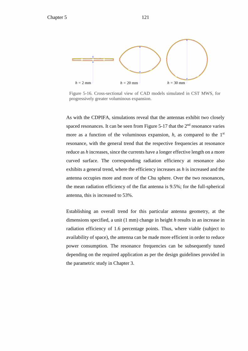
Chapter 5 121
As with the CDPIFA, simulations reveal that the antennas exhibit two closely
spaced resonances. It can be seen from Figure 5-17 that the 2nd resonance varies
more as a function of the voluminous expansion, h, as compared to the 1st
resonance, with the general trend that the respective frequencies at resonance
reduce as h increases, since the currents have a longer effective length on a more
curved surface. The corresponding radiation efficiency at resonance also
exhibits a general trend, where the efficiency increases as h is increased and the
antenna occupies more and more of the Chu sphere. Over the two resonances,
the mean radiation efficiency of the flat antenna is 9.5%; for the full-spherical
antenna, this is increased to 53%.
Establishing an overall trend for this particular antenna geometry, at the
dimensions specified, a unit (1 mm) change in height h results in an increase in
radiation efficiency of 1.6 percentage points. Thus, where viable (subject to
availability of space), the antenna can be made more efficient in order to reduce
power consumption. The resonance frequencies can be subsequently tuned
depending on the required application as per the design guidelines provided in
the parametric study in Chapter 3.
Figure 5-16. Cross-sectional view of CAD models simulated in CST MWS, for
progressively greater voluminous expansion.
h = 2 mm h = 20 mm h = 30 mm

Chapter 5 122
5.3.2. Fabrication
PBF-AM processes comprise the layered, sequential build-up of 3D parts or
structures. This is achieved by decomposing the 3D part into a stack of 2D cross-
sectional layers. A thin layer of powder (ranging from ~10 to ~100 µm) is
Figure 5-17. Simulated resonance frequency of (orange) 1st and (blue) 2nd
resonances as a function of h. Fabricated antennas are annotated.
flat part-
spherical
full-
spherical
1.4
1.6
1.8
2.0
2.2
0 10 20 30
Res
on
ance
Fre
qu
ency
(G
Hz)
h (mm)
Figure 5-18. Simulated radiation efficiency of (orange) 1st and (blue) 2nd resonances
as a function of h. Fabricated antennas are annotated.
flat part-
spherical
full-
spherical
0
20
40
60
80
0 10 20 30
Rad
iati
on E
ffic
iency
(%
)
h (mm)

Chapter 5 123
deposited onto a printing bed and a suitable heat source subsequently used to
melt the cross-sectional layers, one at a time [24]. Two predominant
technologies are SLM and SEBM, with laser and electron beam as the respective
heat sources. In general, slower build times allow for a more robust structure
and a more homogeneous deposition of material throughout the thickness of the
structure; faster build times are (potentially) approachable as the machine
operators gain more confidence in the process timelines required for optimal
build quality.
The SLM process was trialed first, on a Renishaw AM250 printer [99], as it
typically provides higher resolution than SEBM and can yield parts with a
smoother surface finish. A key disadvantage, however, is that SLM is much less
capable of manufacturing overhanging features such as the centrally populated
digits on these antennas. Usually, this limitation is overcome with the use of
sacrificial support structures, analogous to the use of scaffolding in building
construction. Whilst these support structures were intentionally melted in such
a fashion as to reduce their structural integrity, the force needed to remove these
damaged the digits beyond an acceptable degree. Some of the clipped support
structures also left small stubs between two digits which presented an issue in
terms of regulating the current paths on the antenna. A photograph of an antenna
part fabricated with SLM is shown in Figure 5-19, where the partly-removed
support structures can be clearly seen. The support structures which are on the
outside of the surface can easily be buffed away; however, removal of those
behind the digits resulted in distortion of the structure.
With the issue of the support structures proving too problematic, the SEBM
process was used instead, on an Arcam A2 printer [100]. The process is better
suited to the current antenna geometry as the metal powder is pre-sintered before
further processing by the SEBM heat source, removing the need for support
structures. A photograph of an antenna part fabricated with SEBM is shown in
Figure 5-20. Evidently, the surface finish and resolution are much worse than
the laser processed counterpart. This is due to the use of coarser powder layers
with the SEBM process (40-105 µm compared to 15-45 µm for the laser
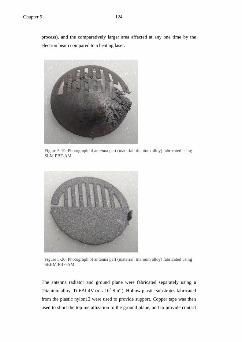
Chapter 5 124
process), and the comparatively larger area affected at any one time by the
electron beam compared to a heating laser.
The antenna radiator and ground plane were fabricated separately using a
Titanium alloy, Ti-6Al-4V (σ ≈ 105 Sm-1). Hollow plastic substrates fabricated
from the plastic nylon12 were used to provide support. Copper tape was then
used to short the top metallization to the ground plane, and to provide contact
Figure 5-19. Photograph of antenna part (material: titanium alloy) fabricated using
SLM PBF-AM.
Figure 5-20. Photograph of antenna part (material: titanium alloy) fabricated using
SEBM PBF-AM.

Chapter 5 125
pads for soldering SMA connectors. Photographs of two fabricated prototypes
are shown in Figure 5-21.
In total, for this project, four iterations of fabrication were performed; each
iteration sought to improve build quality, specifically the surface finish. The
build process for the four SEBM fabricated antennas presented in this chapter
is described as follows:
▪ The Arcam A2 printer was run under a vacuum of about 0.0001 mbar; a
slight amount of helium was inserted into the chamber to help dissipate
the charge induced into the powder bed by the electron beam
▪ All parts were built on a stainless-steel plate, which was heated to 730 °C
by the electron beam before any powder was deposited
▪ For each layer of powder deposited (50 µm thick), the beam was first
defocused and scanned across the layer at a high speed (30 ms-1) with
2.3 kW power, for around 15 seconds, to sinter the powder
▪ Each part area was subsequently melted using a focused beam with a
back and forth raster pattern at a speed of around 0.35 ms-1 with 300 W
power
Figure 5-21. Photograph of two SEBM PBF-AM fabricated antenna prototypes,
shown assembled; (left) full-spherical, (right) flat.

Chapter 5 126
▪ Thereafter, successive powder layers were deposited and the previous
sintering and melting steps repeated until the antenna parts were fully
realized
Eighteen antenna parts (radiator and ground plane separate, i.e. total of nine
antennas) were printed, with a total printing time of 2 hours and 24 minutes. The
entire printing process, including post-processing, was completed within 4
hours. Of the total nine antennas, three each were flat, part-spherical, and full-
spherical. Some parts were damaged or lost in postprocessing, where
pressurized air was used to separate the final melted parts from sintered powder
blocks, due to inexperience; some others were rendered unusable at the
assembly stage due to the application of excessive mechanical force.
5.3.3. Results and Discussion
As pointed out earlier, due to the uncertainties in material properties,
measurements were carried out for return loss and efficiency, and the results
used in a feedback loop to more accurately reflect the construction of the
simulation models in CST MWS. As such, it is not possible at this stage to
compare these AM fabricated antennas to antennas fabricated using
conventional techniques.
Return loss measurements for the antennas were performed using a VNA. The
radiation efficiency was subsequently computed with measurements taken with
the antennas enclosed in a Wheeler cap box, using the constant-loss-resistor
method (see Chapter 2, [86]). Due to low measurement precision, only the
efficiencies for the second resonance were computed, since the absolute figures
are higher and therefore negative/invalid results unlikely. Two sets of
measurements provided for the full-spherical antenna serve to illustrate
measurement precision.
Figure 5-22, Figure 5-23, Figure 5-24, and Figure 5-25 compare the measured
and simulated S11 parameter for the flat, part-spherical and two full-spherical
prototypes, respectively. Simulated efficiency at resonance and measured
efficiency for 20 MHz bandwidth about the resonance frequency are also

Chapter 5 127
displayed. As for the agreement between measurements and simulations, it can
be said that only a general trend is visible, with a considerable and noticeable
departure in the exact values for resonance frequencies, bandwidths, and
efficiencies. These differences may be attributed to the host of difficulties
discussed above in the manufacture and accurate simulation of the antennas.
Nevertheless, with the quality of samples currently available and the state of
knowledge about material properties, an adequate first impression is evident in
the trends observed in simulations and measurements: namely the lowering of
the second resonance frequency as the parameter h is increased, and a
subsequent increase in the radiation efficiency.
Figure 5-22. S11 results for PBF-AM flat CDPIFA; (orange) measured, (blue)
simulated. Radiation efficiency at respective resonance frequencies, for the 2nd
resonance; (purple) measured, (green) simulated.
0
20
40
60
80
-18
-12
-6
0
1.2 1.4 1.6 1.8 2.0
Rad
iati
on E
ffic
iency
(%
)
S1
1(d
B)
Frequency (GHz)
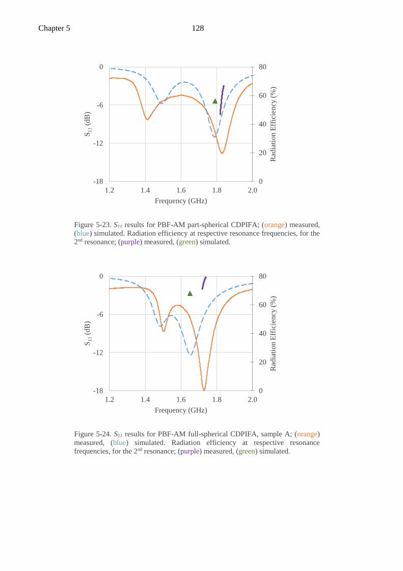
Chapter 5 128
Figure 5-23. S11 results for PBF-AM part-spherical CDPIFA; (orange) measured,
(blue) simulated. Radiation efficiency at respective resonance frequencies, for the
2nd resonance; (purple) measured, (green) simulated.
0
20
40
60
80
-18
-12
-6
0
1.2 1.4 1.6 1.8 2.0
Rad
iati
on
Eff
icie
ncy
(%
)
S1
1(d
B)
Frequency (GHz)
Figure 5-24. S11 results for PBF-AM full-spherical CDPIFA, sample A; (orange)
measured, (blue) simulated. Radiation efficiency at respective resonance
frequencies, for the 2nd resonance; (purple) measured, (green) simulated.
0
20
40
60
80
-18
-12
-6
0
1.2 1.4 1.6 1.8 2.0
Rad
iati
on E
ffic
iency
(%
)
S1
1(d
B)
Frequency (GHz)

Chapter 5 129
Key results for the 2nd resonance of each antenna are summarized in Table 5-2.
Note that the parameter Qratio is not directly applicable to antennas exhibiting
two resonances close together, as there is not yet a consensus in the antenna
community for whether the relationships between Q and bandwidth hold for
such behaviour [19].
Figure 5-25. S11 results for PBF-AM full-spherical CDPIFA, sample B; (orange)
measured, (blue) simulated. Radiation efficiency at respective resonance
frequencies, for the 2nd resonance; (purple) measured, (green) simulated.
0
20
40
60
80
-18
-12
-6
0
1.2 1.4 1.6 1.8 2.0
Rad
iati
on
Eff
icie
ncy
(%
)
S1
1(d
B)
Frequency (GHz)
Table 5-2. Simulated and measured resonant frequency and radiation efficiency at
2nd resonance for PBF-AM fabricated CDPIFAs.
Flat Part-
spherical
Full-
spherical
(sample A)
Full-
spherical
(sample B)
Simulated
frequency (GHz) 1.93 1.79 1.65 -
Measured
frequency (GHz) 1.84 1.83 1.73 1.68
Simulated
efficiency (%) 14 56 68 -
Measured
efficiency (%) 11 59 76 60

Chapter 5 130
Lastly, the realized gain for the fully-spherical CDPIFA was measured in an
anechoic chamber, as described in Chapter 2. Due to the particular feed location
for this antenna, partial power gains were measured with respect to vertical and
horizontal polarizations, and the gain transfer method (see Chapter 2) used
subsequently to compute the total realized gain. Figure 5-26 and Figure 5-27
plot the results for azimuth and elevation planes respectively, measured at 1.7
GHz. As observed with previous ESA gain measurements, there is a large
degree of undulation in the radiation patterns; in particular, there are some
artefacts due to the setup (antenna holder) in the azimuth plane towards the rear
of the antenna. There is, however, good agreement between the two measured
patterns, with a total average difference of 1.7 dB.
Figure 5-26. Realized gain (dBi) for the full-spherical ESA at 1.7 GHz; (orange)
measured – sample A, (green) measured – sample B, (blue) simulated; azimuth
plane. Combined absolute gain (φ and θ components).
180°
-135°
-90°
-45°
0°
45°
90°
135°
-25
-15
-5
5
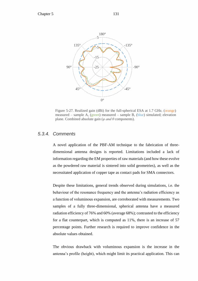
Chapter 5 131
5.3.4. Comments
A novel application of the PBF-AM technique to the fabrication of three-
dimensional antenna designs is reported. Limitations included a lack of
information regarding the EM properties of raw materials (and how these evolve
as the powdered raw material is sintered into solid geometries), as well as the
necessitated application of copper tape as contact pads for SMA connectors.
Despite these limitations, general trends observed during simulations, i.e. the
behaviour of the resonance frequency and the antenna’s radiation efficiency as
a function of voluminous expansion, are corroborated with measurements. Two
samples of a fully three-dimensional, spherical antenna have a measured
radiation efficiency of 76% and 60% (average 68%); contrasted to the efficiency
for a flat counterpart, which is computed as 11%, there is an increase of 57
percentage points. Further research is required to improve confidence in the
absolute values obtained.
The obvious drawback with voluminous expansion is the increase in the
antenna’s profile (height), which might limit its practical application. This can
Figure 5-27. Realized gain (dBi) for the full-spherical ESA at 1.7 GHz. (orange)
measured – sample A, (green) measured – sample B, (blue) simulated; elevation
plane. Combined absolute gain (φ and θ components).
180°
-135°
-90°
-45°
0°
45°
90°
135°
-25
-15
-5
5

Chapter 5 132
be partly addressed by a variation in antenna design where the rear metallization
(ground plane) is kept flat as the top radiator is voluminously expanded. Such a
structure, with a flat ground plane, would be better suited to the majority of
applications where traditional, planar antennas are currently installed since the
antenna can simply be placed on top of an existing metallized surface. However,
due in part to less accurate reproductions of currents on the surface of the new
hemispherical antennas, a sacrifice in the radiation efficiency is to be expected.
Figure 5-28 and Figure 5-29 plot the simulated resonance frequency and
efficiency as a function of the parameter h for these hemispherical variations
(note that for diameter 30 mm, maximum value of h for full-hemisphere is
16 mm instead of 30 mm for full-sphere). The trends in resonance frequency
and radiation efficiency follow those previously established in Figure 5-17 and
Figure 5-18. Over the two resonances, the mean radiation efficiency of the flat
antenna is 9.5%; for the full-hemispherical antenna, this is increased to 40.5%.
Figure 5-28. Simulated resonance frequency of (orange) 1st and (blue) 2nd
resonances as a function of h. Extremes are annotated.
flat full-
hemispheric
al
1.4
1.6
1.8
2.0
2.2
0 4 8 12 16
Res
onan
ce F
requen
cy (
GH
z)
h (mm)
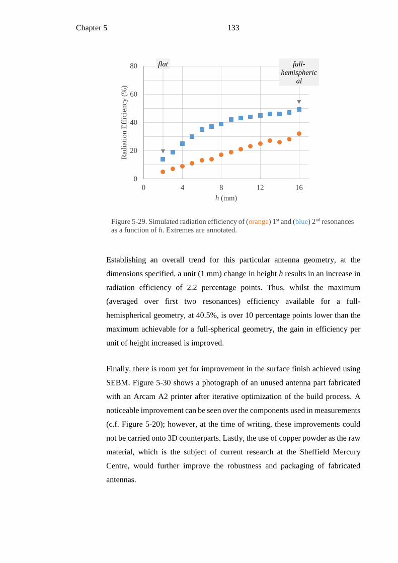
Chapter 5 133
Establishing an overall trend for this particular antenna geometry, at the
dimensions specified, a unit (1 mm) change in height h results in an increase in
radiation efficiency of 2.2 percentage points. Thus, whilst the maximum
(averaged over first two resonances) efficiency available for a full-
hemispherical geometry, at 40.5%, is over 10 percentage points lower than the
maximum achievable for a full-spherical geometry, the gain in efficiency per
unit of height increased is improved.
Finally, there is room yet for improvement in the surface finish achieved using
SEBM. Figure 5-30 shows a photograph of an unused antenna part fabricated
with an Arcam A2 printer after iterative optimization of the build process. A
noticeable improvement can be seen over the components used in measurements
(c.f. Figure 5-20); however, at the time of writing, these improvements could
not be carried onto 3D counterparts. Lastly, the use of copper powder as the raw
material, which is the subject of current research at the Sheffield Mercury
Centre, would further improve the robustness and packaging of fabricated
antennas.
Figure 5-29. Simulated radiation efficiency of (orange) 1st and (blue) 2nd resonances
as a function of h. Extremes are annotated.
flat full-
hemispheric
al
0
20
40
60
80
0 4 8 12 16
Rad
iati
on
Eff
icie
ncy
(%
)
h (mm)
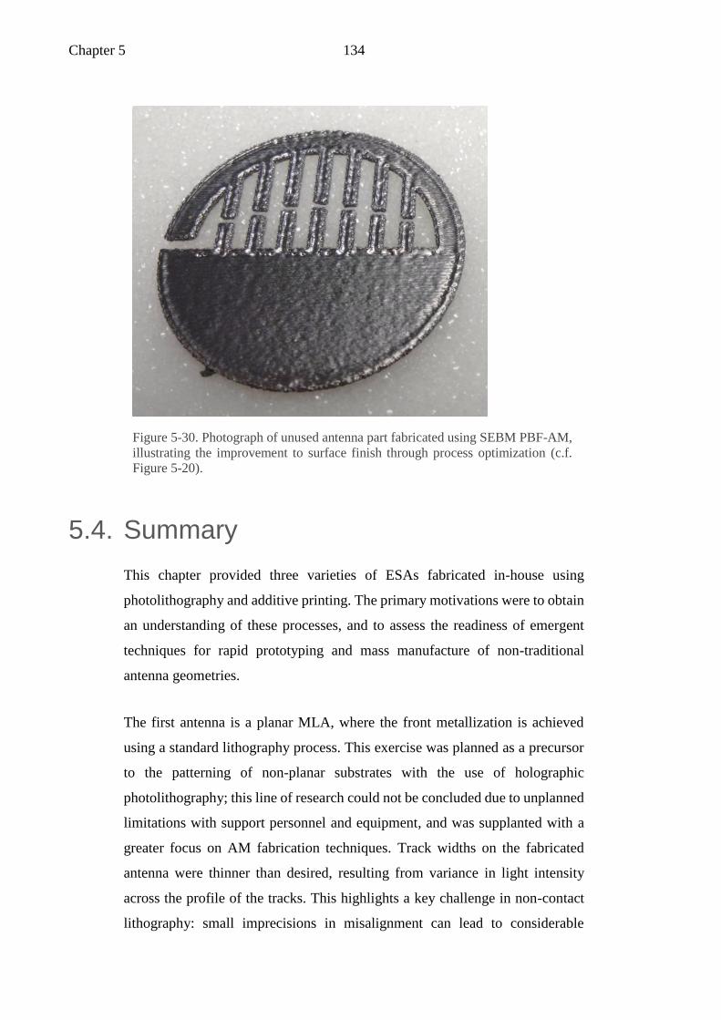
Chapter 5 134
5.4. Summary
This chapter provided three varieties of ESAs fabricated in-house using
photolithography and additive printing. The primary motivations were to obtain
an understanding of these processes, and to assess the readiness of emergent
techniques for rapid prototyping and mass manufacture of non-traditional
antenna geometries.
The first antenna is a planar MLA, where the front metallization is achieved
using a standard lithography process. This exercise was planned as a precursor
to the patterning of non-planar substrates with the use of holographic
photolithography; this line of research could not be concluded due to unplanned
limitations with support personnel and equipment, and was supplanted with a
greater focus on AM fabrication techniques. Track widths on the fabricated
antenna were thinner than desired, resulting from variance in light intensity
across the profile of the tracks. This highlights a key challenge in non-contact
lithography: small imprecisions in misalignment can lead to considerable
Figure 5-30. Photograph of unused antenna part fabricated using SEBM PBF-AM,
illustrating the improvement to surface finish through process optimization (c.f.
Figure 5-20).

Chapter 5 135
changes in final patterned tracks. In a similar vein, such ‘misalignments’ would
be unavoidable for the case of non-planar substrates, where light projected
through standard photolithographic masks diffracts as it exits the mask. This is
a limitation directly overcome by holographic photolithography where
specialist masks are engineered in such a way that emergent light beams can be
locally focused as per the topography of the substrate. Still, the process is unable
to accommodate inherently 3D structures without the use of complex optics to
illuminate areas of a substrate which would lie under a shadow when illuminated
directly from above.
Next, the focus was shifted to the use of AM techniques. At first, two variants
of a dome antenna were fabricated; the substrates were 3D printed with ABS
plastic, and metal tracks subsequently defined by damascening conductive silver
paint onto the substrate. Due to unavoidable print defects in the indented
grooves, the fabricated tracks had poor definition; moreover, the integrity of
connections between the meanderlines and feed lines was compromised during
soldering. As a result, measurements and simulations were not closely aligned.
Finally, the suitability of PBF-AM to directly fabricate metallic prototypes was
investigated. Through this technique, it was possible to fabricate variants of the
CDPIFAs discussed in Chapter 3 with varying heights (or volume).
Measurements show an increase in the radiation efficiency with an increase in
volume; this trend is corroborated with simulations. As the height of the antenna
is increased, the measured radiation efficiencies for a flat, part-spherical, and
full-spherical are 11%, 59%, and 68% (averaged between two samples),
respectively. However, a key limitation in the confidence of the actual
efficiency values is a lack of knowledge of the material properties, and how
these change as the powdered form of raw materials is sintered and melted to
form solid structures.
It can be argued that the techniques used to realize holographic
photolithography may be incorporated into existing industrial processes (of
photolithography). As such, this technique may be better suited in the near term
as a means of fabricating inherently 3D antenna designs (note that underlying

Chapter 5 136
features would still require careful attention; thus, monolithic fabrication would
still not be possible). On the other hand, this past decade has seen exponential
growth in the availability and sophistication of AM techniques, prompting
further research into the fabrication of RF components. As material properties
are better understood and the printing process optimized for electronics (and
especially RF components), PBF-AM is poised to be uniquely suitable for both
rapid prototyping and mass fabrication of antennas.
It is hoped that results presented here catalyze further research into 3D printed
RF components, to drive further maturation of the technology. Possible next
steps are detailed investigation of the material properties under flux, the use of
higher conductivity metals, and continued improvements in the surface finish
and integrity of printed structures. With better understanding of material
properties, reliability analyses would be an immediate next step. Ultimately,
future research can investigate the suitability of AM for mass manufacture of
RF parts.
Chapter 6 137
CHAPTER 6
Conclusions
The aim of this Thesis was to investigate the miniaturization and optimization
of antennas, with considerations for fabrication. Like the many modern antennas
found in mobile electronic devices, an antenna is classed as electrically small if
it operates at a wavelength(s) many times its physical size. More specifically,
taking the radius of the smallest sphere (termed the Chu sphere) that would
completely encapsulate a particular antenna as a, an antenna is classed as
electrically small if the product of the wavenumber k (= 2π/λ) and the parameter
a is less than or equal to 0.5 (also acceptable is ka ≤ 1.0). These values represent
an imaginary spherical boundary containing the first order radiation modes, and
the demarcation between near and far fields of a Hertzian antenna, respectively.
Furthermore, it is widely accepted that as the electrical size of an antenna is
reduced, its performance (in terms of gain, efficiency, and bandwidth)
deteriorates. Generally, the radiation resistance decreases, while the reactive
component of its impedance increases, leading to a poor match with the feed
line or network. The following is a summary of the contributions of this Thesis.
An extensive literature review was presented, covering a range of
miniaturization techniques applied to antennas. The relative advantages and
disadvantages were discussed, and geometrical shaping was identified as a
miniaturization technique which could be intuitively applied and would result
in an antenna that would be simple to fabricate with traditional techniques. To
these ends, a novel, digitated structure was integrated into an IFA to reduce its
electrical size by increasing the antenna’s self-inductance and self-capacitance.
The presence of a large number of tuneable parameters means that the antenna
is well suited for computational optimization algorithms, in order to determine
the best possible impedance match at a desired frequency. Additionally, the

Chapter 6 138
digitated structure can be abstracted into a simpler, two-element design, which
is more suitable for gaining an intuitive understanding. In terms of ease of
manufacture, the uni-planar CDIFA is well suited to traditional fabrication
techniques, such as photolithography and machine etching. Through vias are
employed to feed the antenna, which is a standard process in PCB manufacture.
The absence of lumped reactive components (i.e. chip capacitors or inductors)
further simplifies the fabrication process, lowering manufacturing costs.
Furthermore, the antennas are very low profile, capable of integration directly
into the main PCB of an electronic device. The compact profile of the antenna
is especially suited to handheld mobile devices such as ‘smart’ watches, as
proposed in [114].
Bandwidth enhancement was investigated through a variant of the IFA, with the
new structure closely resembling a PIFA. Termed the CDPIFA, the front
metallization of this antenna is similar to that of the CDIFA; the back is
completely metallized, and therefore does not require any extra processing for
etching techniques. A shorting pin between the radiator and ground sections is
realized with copper tape, though it can be replaced by through vias in future
iterations for increased stability. This antenna structure offers two paths (in
opposing directions) for current flow, the respective lengths of which can be
altered to tune two resonances (with orthogonal polarity) close together. Due
mainly to losses in the substrate, these antennas were found to be very low
efficiency, though the extended bandwidth makes them tolerant to
environmental effects (such as detuning). With their low efficiency, the
antennas are more suited to receive than transmit applications where the signal-
to-noise ratio (SNR) of the incoming signal is often the main limiter in terms of
system performance [22].
It is widely accepted that the ‘best’ compromise between miniaturization and
performance is achieved when an ESA makes full use of the Chu sphere as
determined by its maximum dimension. From the perspective of planar printed
antennas, this implies an increase in height, and a spherical shape. Additive
manufacturing was employed to fabricate variants of the CDPIFA with different
heights, i.e. different fill factors with respect to the Chu sphere. Whilst the
material properties of raw materials used in PBF-AM are not yet fully

Chapter 6 139
characterized, measured results follow theoretical expectations of an increase in
the radiation efficiency as the antenna is made more voluminous.
A planar MLA and a 3D dome antenna with meanderlines were also prototyped
using traditional photolithography and additive printing (and subsequent
metallization with conductive ink), respectively, to develop an intimate
understanding of these fabrication processes alongside research into antenna
miniaturization. Research into the investigation of computer generated
holograms for holographic lithography was subsequently pivoted in favour of
the investigation of the suitability and readiness of AM to prototype ESAs,
primarily due to the opportunity for pioneering measured results of metallic 3D
printed antennas. The PBF-AM process employed for the fabrication of 3D
CDPIFAs is one of the few AM technologies able to directly print metals. As
the process gains further sophistication, it could emerge as a viable option for
the mass manufacture of monolithic, inherently 3D antennas.
6.1. Recommendations for Future Work
This section provides recommendations for the refinement of the results and
ideas presented in the Thesis, and offers some clues for further research work
which can be built on the current work.
6.1.1. Antenna Design
The design methodology employed for antenna miniaturization was based on
geometrical shaping, mainly due to the subsequent ease of manufacture using
traditional methods; this was achieved with the use of a centrally populated
digitated structure in variants of IFAs. A natural extension of the work would
be to investigate the effects of similar structures on other antenna types, such as
loop or slot, and to produce simple predictive models for a first estimate of
antenna performance based on only a few parameters.
Furthermore, having established the usefulness of PBF-AM in rapid prototyping
and potential for mass manufacture, the antenna design stage may be revisited
with added freedoms in terms of inherently 3D designs. For instance, layered

Chapter 6 140
conducting structures may be incorporated in a conformal configuration to
further miniaturize multi-element antenna structures; one example is passive
directive elements on patch or Yagi-Uda type antennas, another is underhanging
capacitive ‘top hats’. The technique is particularly suited to the fabrication of
all-metal, space-filling, wire-type antenna structures generated using
computational algorithms. As printing speeds are increased, PBF-AM can be
integrated more closely into the design process, offering a quick first estimate
of the measured performance of antenna structures designed in CAD and
simulation software such as CST MWS.
6.1.2. Antenna Measurements
A range of different antennas were measured and their results presented in the
course of the discussion thus far. It can be observed that the radiation patterns
obtained for antennas with ka greater than 1 are far better defined than those
whose ka value is less than 1 (i.e. ESAs). Part of the low resolution and precision
of these measurements is the difficulty in correct alignment of the (also)
physically small antenna structures, which can be improved with careful design
of the support apparatus around the AUT.
The use of a copper-clad coaxial feed cable further contributed to any
imprecisions and inaccuracies in the measured results, and made straightforward
simulation of the antenna structures difficult. This is understood to be primarily
due to leakage currents forming on the feed cable and contributing to the EM
fields radiated by the antenna itself. These unwanted effects may be eliminated
with the use of an optical fibre cable instead of the traditional coaxial cables,
together with some type of opto-electric field sensors and RF-optical
transducers [11]. Efforts were made to employ such a measurement setup at the
National Physical Laboratory (NPL) [115, 116], but were ultimately set aside
due to financial constraints. This sort of setup might appear more cost-effective
for potential future work where measurement accuracy is of greater concern.
Chapter 6 141
6.1.3. Additive Manufacture and Material Characterization
It was emphasized that PBF-AM is currently limited only to prototyping of
antennas, due to the dearth of knowledge regarding the EM properties of raw
materials used. This has been identified as a key challenge in the development
of AM in general [110-113], with future progress poised to extend the
application of AM to general mass manufacture. In particular, unknown changes
to material properties during the fabrication process limit the usefulness of raw
material properties. However, existing measurement techniques can be
employed to approximate the electrical permittivity and loss tangent of
dielectrics (e.g. coaxial probe and free-space methods for powders, and
transmission line method for 3D printed solids) [117, 118], as well as the
electrical conductivity of metals [119, 120] fabricated using AM. As process
tolerances are better understood and formalized, such methods can be used to
create a database of the properties of various AM fabricated materials.
It was also demonstrated that there is room for improvement in the quality (in
terms of resolution and surface finish) of parts that can presently be produced.
Further optimization of the printing process, together with the use of materials
traditionally employed for electronics (e.g. copper) can lead to improvements in
the quality of antenna parts realized with the current state of art. (The liaising
Mercury Centre recently started its investigation of copper as a raw material for
AM processes.)
Lack of flexibility in AM parts is currently a major limitation for the technique
compared to processes such as conformal direct-write printing or direct transfer
patterning. Recently though, the concept of four dimensional (4D) printed metal
has been publicized [121, 122], whereby flexible, shape-altering metallic
structures can be realized using enhanced AM techniques; typically, the material
properties are a function of potential external stimuli such as temperature or
pressure. Such advances have the potential to significantly hasten the
proliferation of AM in antenna research and development.

Chapter 6 142
6.2. Concluding Remarks
Through this report, I have presented findings on an intuitive design
methodology covering the integration of digitated structures in inverted-F and
related antennas, and produced pioneering measured results for voluminous
(3D) metallic antennas fabricated with PBF-AM.
A ‘design matrix’ was produced, linking key parameters of a simplified
digitated structure to antenna miniaturization and efficiency; its use as a means
for antenna designers to obtain rapid first estimates over a range of frequencies
without the use of costly computational simulations was also demonstrated.
Several prototypes were fabricated as well, using traditional processes, and
shown to compare well with published antennas from literature. Indeed, there is
scope yet for further formalization of parametric characterization approach,
either in terms of more performance metrics, or a more detailed equivalent
circuit model. While practical challenges endure in the measurement of
electrically small antennas such as those discussed, I remain sanguine that these
will not hold hostage future practical research, and hopeful that the
measurement procedures detailed here would be of aid in such undertakings.
Pilot investigations into PBF-AM fabricated antennas have demonstrated that
the technology is ready for prototyping purposes, justifying further investigation
of this and related AM technologies for RF components. I am optimistic that
these findings will be of aid to future researchers, and that this collaborative
venture will embolden an appetite for further concerted interdisciplinary
teamwork.

143
References
[1] A. B. Frazier, R. O. Warrington, and C. Friedrich, “The miniaturization
technologies: past, present, and future,” IEEE Transactions on Industrial
Electronics, vol. 42, no. 5, pp. 423-430, 1995.
[2] R. R. Schaller, “Moore's law: past, present and future,” IEEE Spectrum, vol. 34,
no. 6, pp. 52-59, 1997.
[3] E. Mollick, “Establishing Moore's law,” IEEE Annals of the History of
Computing, vol. 28, no. 3, pp. 62-75, 2006.
[4] J. U. Knickerbocker et al., “Three-dimensional silicon integration,” IBM Journal
of Research and Development, vol. 52, no. 6, pp. 553-569, 2008.
[5] R. R. Tummala and M. Swaminathan, Introduction to System-on-Package (SOP):
Miniaturization of the Entire System. USA: McGraw-Hill, 2008.
[6] R. W. Keyes, “Physical limits in digital electronics,” Proceedings of the IEEE,
vol. 63, no. 5, pp. 740-767, 1975.
[7] R. W. Keyes, “Fundamental limits of silicon technology,” Proceedings of the
IEEE, vol. 89, no. 3, pp. 227-239, 2001.
[8] Y. Nishi, “Lithium ion secondary batteries; past 10 years and the future,” Journal
of Power Sources, vol. 100, no. 1, pp. 101-106, 2001.
[9] K. Lahiri, A. Raghunathan, S. Dey, and D. Panigrahi, “Battery-driven system
design: a new frontier in low power design,” in Proceedings of ASP-DAC/VLSI
Design 2002. 7th Asia and South Pacific Design Automation Conference and 15h
International Conference on VLSI Design, Bangalore, India, 2002, pp. 261-267.
[10] R. Nagai, F. Kita, and M. Yamada, “Development of highly reliable high-capacity
batteries for mobile devices and small-to medium-sized batteries for industrial
applications,” Energy, vol. 450, no. 400, p. 350, 2003.
[11] K. Fujimoto and H. Morishita, Modern Small Antennas. USA: Cambridge
University Press, 2014.
[12] A. Mieczakowski, T. Goldhaber, and J. Clarkson, “Culture, communication and
change: Summary of an investigation of the use and impact of modern media and
technology in our lives,” Engineering Design Centre, University of Cambridge,
Cambridge, 2011.
144
[13] H. Z. Shi and A. Tennant, “Simultaneous, multichannel, spatially directive data
transmission using direct antenna modulation,” IEEE Transactions on Antennas
and Propagation, Article vol. 62, no. 1, pp. 403-410, Jan 2014.
[14] Y. Ding and V. Fusco, “A review of directional modulation technology,”
International Journal of Microwave and Wireless Technologies, vol. 8, no. 7, pp.
981-993, Nov 2016.
[15] P. S. Carter and H. H. Beverage, “Early history of the antennas and propagation
field until the end of World War I: Part I - antennas,” Proceedings of the IRE, vol.
50, no. 5, pp. 679-682, 1962.
[16] J. D. Kraus, Antennas, 2nd ed. USA: McGraw-Hill, 1988.
[17] Apple Inc. (2017, Nov. 7). Apple Watch series 2 - technical specifications
[online]. Available: https://support.apple.com/kb/SP746. (Accessed: 2017/12/11)
[18] H. A. Wheeler, “Fundamental limitations of small antennas,” Proceedings of the
IRE, vol. 35, no. 12, pp. 1479-1484, 1947.
[19] S. R. Best, “Small and fractal antennas,” in Modern Antenna Handbook, C. A.
Balanis, Ed. USA: John Wiley & Sons, 2008, pp. 475-528.
[20] J. L. Volakis, C. C. Chen, and K. Fujimoto, Small Antennas: Miniaturization
Techniques and Applications. USA: McGraw-Hill, 2010.
[21] R. C. Hansen and R. E. Collin, Small Antenna Handbook. USA: John Wiley &
Sons, 2011.
[22] C. A. Balanis, Antenna Theory: Analysis and Design, 4th ed. USA: John Wiley &
Sons, 2016.
[23] A. Maiden, “Lithography in three dimensions using computer-generated
holograms,” Ph.D. dissertation, School of Engineering, Durham University, 2005.
[24] I. Gibson, D. W. Rosen, and B. Stucker, Additive Manufacturing Technologies:
Rapid Prototyping to Direct Digital Manufacturing. USA: Springer, 2010.
[25] J. Hoerber, J. Glasschroeder, M. Pfeffer, J. Schilp, M. Zaeh, and J. Franke,
“Approaches for additive manufacturing of 3D electronic applications,” Procedia
CIRP, vol. 17, pp. 806-811, 2014.
[26] IEEE Standard for Definitions of Terms for Antennas, IEEE Std 145-2013
(Revision of IEEE Std 145-1993), 2014.

145
[27] L. J. Chu, “Physical limitations of omni-directional antennas,” Journal of Applied
Physics, vol. 19, no. 12, pp. 1163-1175, 1948.
[28] H. A. Wheeler, “The radiansphere around a small antenna,” Proceedings of the
IRE, vol. 47, no. 8, pp. 1325-1331, 1959.
[29] J. S. McLean, “A re-examination of the fundamental limits on the radiation Q of
electrically small antennas,” IEEE Transactions on Antennas and Propagation,
vol. 44, no. 5, pp. 672-676, 1996.
[30] R. F. Harrington, “Effect of antenna size on gain, bandwidth, and efficiency,”
Journal of Research of the National Bureau of Standards, vol. 64D, no. 1, pp. 1-
12, 1960.
[31] R. C. Hansen, “Fundamental limitations in antennas,” Proceedings of the IEEE,
vol. 69, no. 2, pp. 170-182, 1981.
[32] H. L. Thal, “New radiation Q limits for spherical wire antennas,” IEEE
Transactions on Antennas and Propagation, vol. 54, no. 10, pp. 2757-2763, 2006.
[33] M. Gustafsson, C. Sohl, and G. Kristensson, “Physical limitations on antennas of
arbitrary shape,” Proceedings of the Royal Society A: Mathematical Physical and
Engineering Sciences, vol. 463, no. 2086, pp. 2589-2607, 2007.
[34] H. R. Stuart, S. R. Best, and A. D. Yaghjian, “Limitations in relating quality factor
to bandwidth in a double resonance small antenna,” IEEE Antennas and Wireless
Propagation Letters, vol. 6, pp. 460-463, 2007.
[35] D. Sievenpiper et al., “Experimental validation of performance limits and design
guidelines for small antennas,” IEEE Transactions on Antennas and Propagation,
vol. 60, no. 1, pp. 8-19, 2012.
[36] S. E. Sussman-Fort and R. M. Rudish, “Non-Foster impedance matching of
electrically-small antennas,” IEEE Transactions on Antennas and Propagation,
vol. 57, no. 8, pp. 2230-2241, 2009.
[37] J. P. Gianvittorio and Y. Rahmat-Samii, “Fractal antennas: a novel antenna
miniaturization technique, and applications,” IEEE Antennas and Propagation
Magazine, vol. 44, no. 1, pp. 20-36, 2002.
[38] J. M. Johnson and V. Rahmat-Samii, “Genetic algorithms in engineering
electromagnetics,” IEEE Antennas and Propagation Magazine, vol. 39, no. 4, pp.
7-21, 1997.
[39] D. Sievenpiper, “Review of theory, fabrication, and applications of high
impedance ground planes,” in Metamaterials: Physics and Engineering

146
Explorations, N. Engheta and R. W. Ziolkowski, Eds. USA: John Wiley & Sons,
2006, pp. 287-376.
[40] H. Liu, K. L. Ford, and R. J. Langley, “Miniaturised artificial magnetic conductor
design using lumped reactive components,” Electronics Letters, vol. 45, no. 6, pp.
294-295, 2009.
[41] H. L. Liu, K. L. Ford, and R. J. Langley, “Design methodology for a miniaturized
frequency selective surface using lumped reactive components,” IEEE
Transactions on Antennas and Propagation, vol. 57, no. 9, pp. 2732-2738, 2009.
[42] R. W. Ziolkowski and A. Erentok, “Metamaterial-based efficient electrically
small antennas,” IEEE Transactions on Antennas and Propagation, vol. 54, no.
7, pp. 2113-2130, 2006.
[43] A. Erentok and R. W. Ziolkowski, “Metamaterial-inspired efficient electrically
small antennas,” IEEE Transactions on Antennas and Propagation, vol. 56, no.
3, pp. 691-707, 2008.
[44] Y. D. Dong and T. Itoh, “Metamaterial-based antennas,” Proceedings of the IEEE,
vol. 100, no. 7, pp. 2271-2285, 2012.
[45] H. R. Stuart and C. Tran, “Small spherical antennas using arrays of
electromagnetically coupled planar elements,” IEEE Antennas and Wireless
Propagation Letters, vol. 6, pp. 7-10, 2007.
[46] S. R. Best and D. L. Hanna, “A performance comparison of fundamental small-
antenna designs,” IEEE Antennas and Propagation Magazine, vol. 52, no. 1, pp.
47-70, 2010.
[47] J. Anguera, L. Boada, C. Puente, C. Borja, and J. Soler, “Stacked H-shaped
microstrip patch antenna,” IEEE Transactions on Antennas and Propagation, vol.
52, no. 4, pp. 983-993, 2004.
[48] L. M. Feldner, C. T. Rodenbeck, C. G. Christodoulou, and N. Kinzie, “Electrically
small frequency-agile PIFA-as-a-package for portable wireless devices,” IEEE
Transactions on Antennas and Propagation, vol. 55, no. 11, pp. 3310-3319, 2007.
[49] K. L. Wong, C. H. Chang, and Y. C. Lin, “Printed PIFA EM compatible with
nearby conducting elements,” IEEE Transactions on Antennas and Propagation,
vol. 55, no. 10, pp. 2919-2922, 2007.
[50] R. B. Waterhouse and D. Novak, “Uni-planar folded meander line slot antenna
with short circuit,” IEEE Transactions on Antennas and Propagation, vol. 54, no.
11, pp. 3549-3551, 2006.

147
[51] R. N. Simons, Coplanar Waveguide Circuits, Components, and Systems. John
Wiley & Sons, 2001.
[52] W. Hong and K. Sarabandi, “Low profile miniaturized planar antenna with
omnidirectional vertically polarized radiation,” IEEE Transactions on Antennas
and Propagation, vol. 56, no. 6, pp. 1533-1540, 2008.
[53] S. I. Latif, L. Shafai, and S. K. Sharma, “Bandwidth enhancement and size
reduction of microstrip slot antennas,” IEEE Transactions on Antennas and
Propagation, vol. 53, no. 3, pp. 994-1003, 2005.
[54] C. Hosung, R. L. Rogers, and L. Hao, “Design of electrically small wire antennas
using a pareto genetic algorithm,” IEEE Transactions on Antennas and
Propagation, vol. 53, no. 3, pp. 1038-1046, 2005.
[55] E. E. Altshuler, “Electrically small genetic antennas immersed in a dielectric,” in
IEEE Antennas and Propagation Society Symposium, 2004, Monterey, USA,
2004, vol. 3, pp. 2317-2320.
[56] E. E. Altshuler, “A method for matching an antenna having a small radiation
resistance to a 50-ohm coaxial line,” IEEE Transactions on Antennas and
Propagation, vol. 53, no. 9, pp. 3086-3089, 2005.
[57] C. T. Rodenbeck, “Planar miniature RFID antennas suitable for integration with
batteries,” IEEE Transactions on Antennas and Propagation, vol. 54, no. 12, pp.
3700-3706, 2006.
[58] U. Deepak, P. Mohanan, C. M. Nijas, and T. K. Roshna, “Compact CPW fed
electrically small antenna for WLAN application,” Electronics Letters, vol. 50,
no. 2, pp. 62-64, 2014.
[59] B. Ghosh, S. M. Haque, D. Mitra, and S. Ghosh, “A loop loading technique for
the miniaturization of non-planar and planar antennas,” IEEE Transactions on
Antennas and Propagation, vol. 58, no. 6, pp. 2116-2121, 2010.
[60] M. C. Tang and R. W. Ziolkowski, “A study of low-profile, broadside radiation,
efficient, electrically small antennas based on complementary split ring
resonators,” IEEE Transactions on Antennas and Propagation, vol. 61, no. 9, pp.
4419-4430, 2013.
[61] N. Zhu and R. W. Ziolkowski, “Metamaterial-inspired, near-field resonant
parasitic GPS antennas: designs and experiments,” in 2011 IEEE International
Symposium on Antennas and Propagation (APSURSI), Spokane, USA, 2011, pp.
658-660.

148
[62] N. Zhu and R. W. Ziolkowski, “Broad-bandwidth, electrically small antenna
augmented with an internal non-Foster element,” IEEE Antennas and Wireless
Propagation Letters, vol. 11, pp. 1116-1120, 2012.
[63] S. Zhu, K. L. Ford, A. Tennant, and R. J. Langley, “Miniaturised split ring antenna
over loaded AMC surface,” in 2010 Loughborough Antennas & Propagation
Conference, 2010, pp. 305-308.
[64] S. Zhu, D. G. Holtby, K. L. Ford, A. Tennant, and R. J. Langley, “Compact low
frequency varactor loaded tunable SRR antenna,” IEEE Transactions on Antennas
and Propagation, vol. 61, no. 4, pp. 2301-2304, 2013.
[65] O. S. Kim, “Low-Q electrically small spherical magnetic dipole antennas,” IEEE
Transactions on Antennas and Propagation, vol. 58, no. 7, pp. 2210-2217, 2010.
[66] M. D. Chiou and S. Y. Chen, “An electrically small planar antenna using
complementary split-ring resonators,” in 2012 International Symposium on
Antennas and Propagation (ISAP), Nagoys, Japan, 2012, pp. 1313-1316.
[67] K. N. Madsen, Y. Zhou, and D. F. Sievenpiper, “A simplified low-Q electrically
small magnetic dipole antenna,” IEEE Antennas and Wireless Propagation
Letters, vol. 15, pp. 1975-1978, 2016.
[68] M. T. Lee, K. M. Luk, K. W. Leung, and M. K. Leung, “A small dielectric
resonator antenna,” IEEE Transactions on Antennas and Propagation, vol. 50, no.
10, pp. 1485-1487, 2002.
[69] K. Y. Hui and K. M. Luk, “A miniature dielectric resonator loaded patch antenna,”
IEEE Transactions on Antennas and Propagation, vol. 53, no. 6, pp. 2118-2122,
2005.
[70] K. Y. Hui and K. M. Luk, “Bandwidth enhancement of small dielectric resonator
loaded patch antenna,” IEEE Transactions on Antennas and Propagation, vol. 54,
no. 6, pp. 1882-1885, 2006.
[71] D. E. Anagnostou, A. A. Gheethan, A. K. Amert, and K. W. Whites, “A direct-
write printed antenna on paper-based organic substrate for flexible displays and
WLAN applications,” Journal of Display Technology, vol. 6, no. 11, pp. 558-564,
2010.
[72] J. J. Adams et al., “Conformal printing of electrically small antennas on three-
dimensional surfaces,” Advanced Materials, vol. 23, no. 11, pp. 1335-1340, 2011.
[73] J. J. Toriz-Garcia et al., “Fabrication of a 3D electrically small antenna using
holographic photolithography,” Journal of Micromechanics and
Microengineering, vol. 23, no. 5, p. 5, 2013, Art. no. 055010.

149
[74] C. Pfeiffer, X. Xu, S. R. Forrest, and A. Grbic, “Direct transfer patterning of
electrically small antennas onto three-dimensionally contoured substrates,”
Advanced Materials, vol. 24, no. 9, pp. 1166-1170, 2012.
[75] M. Kgwadi, C. J. Vourch, D. J. Harrison, and T. D. Drysdale, “On-demand
printing of antennas for TV white-space communications,” in 2014
Loughborough Antennas and Propagation Conference (LAPC), Loughborough,
UK, 2014, pp. 553-556.
[76] I. T. Nassar and T. M. Weller, “An electrically-small, 3-D cube antenna fabricated
with additive manufacturing,” in 2013 IEEE Radio and Wireless Symposium,
2013, pp. 262-264.
[77] O. S. Kim, “3D printing electrically small spherical antennas,” in 2013 IEEE
Antennas and Propagation Society International Symposium (APSURSI),
Orlando, USA, 2013, pp. 776-777.
[78] N. Arnal et al., “3D digital manufacturing and characterization of antennas
integrated in mobile handset covers,” in 2015 IEEE 16th Annual Wireless and
Microwave Technology Conference (WAMICON), Cocoa Beach, USA, 2015, pp.
1-5.
[79] H. Yuxiao, C. Oakley, P. Chahal, J. Albrecht, and J. Papapolymerou, “Aerosol Jet
printed 24 GHz end-fire quasi-Yagi-Uda antenna on a 3-D printed cavity
substrate,” in 2017 International Workshop on Antenna Technology: Small
Antennas, Innovative Structures, and Applications (iWAT), Athens, Greece, 2017,
pp. 179-182.
[80] CST Computer Simulation Technology AG. (n.d.). CST Microwave Studio - 3D
EM simulation software [online]. Available:
https://www.cst.com/products/cstmws. (Accessed: 2017/12/11)
[81] D. M. Pozar, Microwave Engineering, 4th ed. USA: John Wiley & Sons, 2011.
[82] E. Bogatin, Signal and Power Integrity – Simplified, 2nd ed. USA: Prentice Hall,
2010.
[83] Rhode and Schwarz GmbH and Co. KG. (n.d.). Brochures and Data Sheets for
Product HF906 - Rhode and Schwarz United Kingdom [online]. Available:
https://www.rohde-schwarz.com/uk/brochure-datasheet/hf906/. (Accessed:
2017/12/11)
[84] E. Newman, P. Bohley, and C. Walter, “Two methods for the measurement of
antenna efficiency,” IEEE Transactions on Antennas and Propagation, vol. 23,
no. 4, pp. 457-461, 1975.

150
[85] D. M. Pozar and B. Kaufman, “Comparison of three methods for the measurement
of printed antenna efficiency,” IEEE Transactions on Antennas and Propagation,
vol. 36, no. 1, pp. 136-139, 1988.
[86] D. Agahi and W. Domino, “Efficiency measurements of portable-handset
antennas using the Wheeler cap,” Applied Microwave and Wireless, vol. 36, no.
1, pp. 34-42, 2000.
[87] H. J. Levinson, Principles of Lithography, 3rd ed. USA: SPIE Press, 2010.
[88] K. Seshan, Ed. Handbook of Thin Film Deposition: Processes and Techniques,
2nd ed. Noyes Publications, 2002.
[89] Y. N. Xia and G. M. Whitesides, “Soft lithography,” Annual Review of Materials
Science, vol. 28, no. 1, pp. 153-184, 1998.
[90] T. Ito and S. Okazaki, “Pushing the limits of lithography,” Nature, vol. 406, no.
6799, pp. 1027-1031, 2000.
[91] D. Radtke and U. D. Zeitner, “Laser-lithography on non-planar surfaces,” Optics
Express, vol. 15, no. 3, pp. 1167-1174, 2007.
[92] M. J. Madou, Manufacturing Techniques for Microfabrication and
Nanotechnology (Fundamentals of Microfabrication and Nanotechnology Vol. 2).
CRC Press, 2011.
[93] J. W. Goodman, Introduction to Fourier Optics, 2nd ed. USA: McGraw-Hill,
1996.
[94] W. E. Frazier, “Metal additive manufacturing: a review,” Journal of Materials
Engineering and Performance, vol. 23, no. 6, pp. 1917-1928, 2014.
[95] C. Korner, “Additive manufacturing of metallic components by selective electron
beam melting – a review,” International Materials Reviews, vol. 61, no. 5, pp.
361-377, 2016.
[96] F. Calignano et al., “Overview on additive manufacturing technologies,”
Proceedings of the IEEE, vol. 105, no. 4, pp. 593-612, 2017.
[97] Standard Terminology for Additive Manufacturing – General Principles –
Terminology, ISO/ASTM52900-15, 2015.
[98] University of Sheffield. (n.d.). About us - Engineering at Sheffield - Faculties -
The University of Sheffield [online]. Available:
https://www.sheffield.ac.uk/faculty/engineering/about-us/research. (Accessed:
2017/12/11)
151
[99] Renishaw PLC. (n.d.). Renishaw: enhancing efficiency in manufacturing and
healthcare [online]. Available: http://www.renishaw.com/en. (Accessed:
2017/12/11)
[100] Arcam AB. (n.d.). Arcam AB - Additive Manufacturing for Implants and
Aerospace, EBM [online]. Available: http://www.arcam.com. (Accessed:
2017/12/11)
[101] EOS GmbH. (n.d.). EOS e-Manufacturing Solutions: Industrial 3D Printing
[online]. Available: https://www.eos.info/en. (Accessed: 2017/12/11)
[102] MakerBot Industries LLC. (n.d.). Connected 3D Printing Solutions [online].
Available: https://www.makerbot.com. (Accessed: 2017/12/11)
[103] Y. L. Kuo and K. L. Wong, “Coplanar waveguide-fed folded inverted-F antenna
for UMTS application,” Microwave and Optical Technology Letters, vol. 32, no.
5, pp. 364-366, 2002.
[104] M. C. Huynh and W. Stutzman, “Ground plane effects on planar inverted-F
antenna (PIFA) performance,” IEE Proceedings - Microwaves, Antennas and
Propagation, vol. 150, no. 4, pp. 209-213, 2003.
[105] S. R. Best, “A discussion on small antennas operating with small finite ground
planes,” in IEEE International Workshop on Antenna Technology Small Antennas
and Novel Metamaterials, 2006., 2006, pp. 152-155.
[106] J. T. Bernhard, J. J. Adams, M. D. Anderson, and J. M. Martin, “Measuring
electrically small antennas: details and implications,” in 2009 IEEE International
Workshop on Antenna Technology (iWAT), Santa Monica, USA, 2009, pp. 1-4.
[107] The Editors of Encyclopædia Britannica. (2013, Oct. 04). damascening [online].
Available: https://www.britannica.com/art/damascening. (Accessed: 2017/12/11)
[108] M. I. Jais et al., “Design analysis of 2.45 GHz meander line antenna (MLA),” in
2012 3rd International Conference on Intelligent Systems Modelling and
Simulation (ISMS), Kota Kinabalu, Malaysia, 2012, pp. 628-631.
[109] J. J. Adams, S. C. Slimmer, T. F. Malkowski, E. B. Duoss, J. A. Lewis, and J. T.
Bernhard, “Comparison of spherical antennas fabricated via conformal printing:
helix, meanderline, and hybrid designs,” IEEE Antennas and Wireless
Propagation Letters, vol. 10, pp. 1425-1428, 2011.
[110] Wohlers Associates Inc. (n.d.). Roadmap for Additive Manufacturing: Identifying
the Future of Freeform Processing [online]. Available:
https://wohlersassociates.com/roadmap2009.html. (Accessed: 2017/12/11)

152
[111] Y. Huang, M. C. Leu, J. Mazumder, and A. Donmez, “Additive manufacturing:
current state, future potential, gaps and needs, and recommendations,” Journal of
Manufacturing Science and Engineering, vol. 137, no. 1, Feb 2015, Art. no.
014001.
[112] J. A. Slotwinski and E. J. Garboczi, “Metrology needs for metal additive
manufacturing powders,” JOM, vol. 67, no. 3, pp. 538-543, 2015.
[113] S. K. Everton, M. Hirsch, P. Stravroulakis, R. K. Leach, and A. T. Clare, “Review
of in-situ process monitoring and in-situ metrology for metal additive
manufacturing,” Materials & Design, vol. 95, pp. 431-445, 2016.
[114] S. Mufti, A. Tennant, and L. Seed, “Compact electrically small antenna for smart
watch application,” in 2015 University of Sheffield Engineering Symposium
(USES), Sheffield, UK, 2015.
[115] T. H. Loh and M. Alexander, “New facility for minimally invasive measurements
of electrically small antennas,” in 2008 Loughborough Antennas and Propagation
Conference (LAPC), Loughboroug, UK, 2008, pp. 313-316.
[116] M. Alexander, T. H. Loh, and A. L. Betancort, “Measurement of electrically small
antennas via optical fibre,” in 2009 Loughborough Antennas and Propagation
Conference (LAPC), Loughborough, UK, 2009, pp. 653-656.
[117] Keysight. (2017, Mar. 07). Basics of Measuring the Dielectric Properties of
Materials (Application Note 5989-2589EN) [online]. Available:
http://literature.cdn.keysight.com/litweb/pdf/5989-2589EN.pdf. (Accessed:
2017/12/11)
[118] J. Baker-Jarvis, M. D. Janezic, and D. C. Degroot, “High-frequency dielectric
measurements,” IEEE Instrumentation & Measurement Magazine, vol. 13, no. 2,
pp. 24-31, 2010.
[119] Keysight. (2016, Jan. 28). Challenges and Solutions for Material
Science/Engineering Testing Applications (Application Note 992-1182EN)
[online]. Available: https://literature.cdn.keysight.com/litweb/pdf/5992-
1182EN.pdf. (Accessed: 2017/12/11)
[120] M. B. Heaney, “Electrical conductivity and resistivity,” in Electrical
Measurement, Signal Processing, and Displays, J. G. Webster, Ed. USA: CRC
Press, 2003, pp. 7-1 - 7-14.
[121] NASA Jet Propulsion Laboratory. (2017, Apr. 18). 'Space Fabric' Links Fashion
and Engineering [online]. Available:
https://www.jpl.nasa.gov/news/news.php?feature=6816. (Accessed: 2017/12/11)

153
[122] Z. X. Khoo et al., “3D printing of smart materials: a review on recent progresses
in 4D printing,” Virtual and Physical Prototyping, vol. 10, no. 3, pp. 103-122,
2015.

154
(This page intentionally left blank.)

155
Appendix – Computer Generated Holograms
This appendix provides an executive summary of the work done in the early
stages of this project towards the realization of computer generated holograms
(CGH). CGH are photolithographic masks synthesized using computational
iterative algorithms, and may be manifested either digitally or physically.
Popularized by Gabor in 1948, the concept of holography is centred on
recording the interference pattern as an object is illuminated with a light source
and the resulting wave-front intersected with a reference wave-front (the
original illumination beam). The CGH mask stores these interference patterns;
upon illumination by a suitable coherent light source, a virtual recreation of the
original information is possible. The following sections give a brief overview
of the laboratory setup, CGH algorithm, and the resulting CGH mask and
captured optical field; lastly, some resources for further reading are listed.
Laboratory Setup
The laboratory setup used for the exposure stage in holographic lithography is
shown in Figure A-1.
The optical source is a 110 mW rated laser (wavelength: 405 nm); the laser beam
is subsequently expanded and collimated to be able to cover the entire area –
Figure A-1. Laboratory setup for holographic photolithography; exposure stage.
Laser Ray shaping
optics
Beam-splitter Spatial line
modulator
Substrate to PC
z
CGH

156
roughly 133 mm2 (1920 by 1080 array of 8 μm2 pixels) – of the spatial line
modulator (digital projector) where the CGH is displayed. The desired image is
projected a distance z cm from the CGH, where the antenna substrate is placed
(metallized and covered with photoresist). In order to characterize the projected
image, a specialized camera was placed in lieu of actual substrates, at the
appropriate distance(s) away from the CGH.
Iterative Algorithm
The algorithm is initiated by creating a seed image based on the desired image
to be propagated onto the observation plane. The seed image consists of an
amplitude term closely resembling the desired image and a randomly generated
phase component.
The resultant complex field is propagated to the far-field holographic plane
using a transfer function, based on the angular spectrum propagation of optical
fields. At the hologram plane, the phase information is retained, but amplitude
is replaced by random values, or unity.
The new resultant field is subsequently propagated back to the image plane
using an inverse transfer function. At this stage, the amplitude is compared to
that of the desired image; if the error is above a certain threshold value, one of
two alternating constraints is applied.
In the first case, phase information is retained and the amplitude replaced with
the desired image amplitude. The resultant field replaces the original seed
image, and the algorithm is repeated. In the second case, the phase information
is combined with the phase of the original seed image, and the amplitude
replaced with the desired image amplitude. The resultant field replaces the
original seed image, and the algorithm is repeated. It was found experimentally
that the alternating of constraints reduced stagnation in error reduction between
the desired and propagated image amplitudes.
Once the error is acceptably low, the algorithm is terminated, and the phase
information obtained at the holographic plane is saved as the CGH mask, after
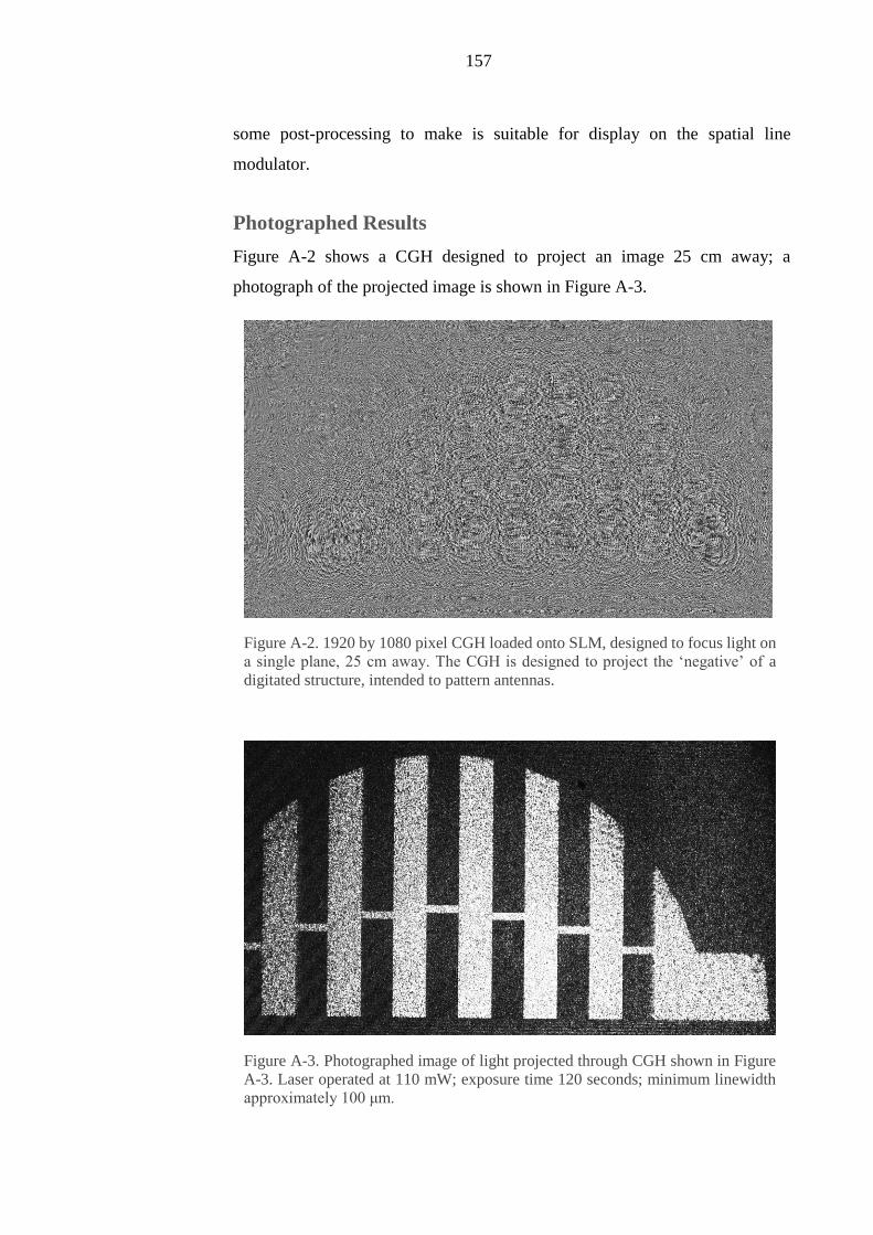
157
some post-processing to make is suitable for display on the spatial line
modulator.
Photographed Results
Figure A-2 shows a CGH designed to project an image 25 cm away; a
photograph of the projected image is shown in Figure A-3.
Figure A-2. 1920 by 1080 pixel CGH loaded onto SLM, designed to focus light on
a single plane, 25 cm away. The CGH is designed to project the ‘negative’ of a
digitated structure, intended to pattern antennas.
Figure A-3. Photographed image of light projected through CGH shown in Figure
A-3. Laser operated at 110 mW; exposure time 120 seconds; minimum linewidth
approximately 100 μm.

158
Further Reading
J. R. Fienup, “Phase retrieval algorithms: a comparison, “ Applied Optics, vol.
21, no. 15, pp. 2758-2769, 1982.
J. W. Goodman, Introduction to Fourier Optics, 2nd ed. USA: McGraw-Hill,
1996.
A. Maiden, “Lithography in three dimensions using computer-generated
holograms,” Ph.D. dissertation, School of Engineering, Durham University,
2005.
D. G. Voelz, Computational Fourier Optics: a MATLAB Tutorial. USA: SPIE
Press, 2011.
J. J. Cowling et al., “Three-dimensional holographic lithography by an iterative
algorithm,” Optics Letters, vol. 36, no. 13, pp. 2495-2497, 2011.
J. Cowling, “An Iterative Algorithm for Lithography on Three-Dimensional
Surfaces,” Ph.D. dissertation, School of Engineering and Computing Sciences,
Durham University, 2015.