miniaturised ultra wide band (uwb)antenna with
TRANSCRIPT

1
MINIATURISED ULTRA WIDE BAND (UWB)ANTENNA WITH BAND REJECTION CONFIGURABILITY
A Project report submitted in partial fulfillment of the requirements for
the award of the degree of
BACHELOR OF TECHNOLOGY
IN
ELECTRONICS AND COMMUNICATION ENGINEERING
Submitted by
K.V.Ratnavathi(316126512050) V.Sai Sandeep(316126512055)
SK.Riyaz Basha(316126512051) B.Suresh(316126512066)
Under the guidance of
Ms.M.Nirmala, M.Tech (ph.d)
Assistant Professor
DEPARTMENT OF ELECTRONICS AND COMMUNICATION ENGINEERING
ANIL NEERUKONDA INSTITUTE OF TECHNOLOGY AND SCIENCES
(UGC AUTONOMOUS)
(Permanently Affiliated to AU, Approved by AICTE and Accredited by NBA & NAAC with ‘A’ Grade
Sangivalasa, Bheemili mandal, visakhapatnam dist.(A.P)
2019-2020
2
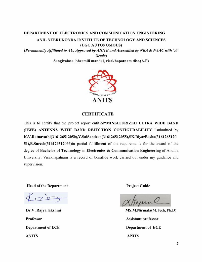
DEPARTMENT OF ELECTRONICS AND COMMUNICATION ENGINEERING
ANIL NEERUKONDA INSTITUTE OF TECHNOLOGY AND SCIENCES (UGC AUTONOMOUS)
(Permanently Affiliated to AU, Approved by AICTE and Accredited by NBA & NAAC with ‘A’ Grade)
Sangivalasa, bheemili mandal, visakhapatnam dist.(A.P)
CERTIFICATE
This is to certify that the project report entitled“MINIATURIZED ULTRA WIDE BAND
(UWB) ANTENNA WITH BAND REJECTION CONFIGURABILITY ”submitted by
K.V.Ratnavathi(316126512050),V.SaiSandeep(316126512055),SK.RiyazBasha(3161265120
51),B.Suresh(316126512066)in partial fulfillment of the requirements for the award of the
degree of Bachelor of Technology in Electronics & Communication Engineering of Andhra
University, Visakhapatnam is a record of bonafide work carried out under my guidance and
supervision.
Head of the Department Project Guide
Dr.V .Rajya lakshmi MS.M.Nirmala(M.Tech, Ph.D)
Professor Assistant professor
Department of ECE Department of ECE
ANITS ANITS

3
ACKNOWLEDGEMENT
I thank to my guide Ms.M.Nirmala, Assistant professor, Department of Electronics and
Communication Engineering, Anil Neerukonda Institute of Technology and Sciences (ANITS),
for spending her valuable time to review and analyze my project at every stage. I consider myself
extremely fortunate to have the opportunity of associating with her.
I express my deep sense of gratitude and respect to our beloved Head of the Department, Dr. V.
RAJYA LAKSHMI, Department of Electronics and Communication Engineering, for his
inspiration, adroit guidance and constructive criticism and providing us with the required
facilities for the partial completion of the project work.
I am very much thankful to the Principal and Management, ANITS, Sangivalasa, for their
encouragement and cooperation to carry out this work. I express my thanks to all teaching staff
of Dept. of ECE for providing a great assistance in accomplishment of my project.
I also express my thanks to all the non-teaching staff of Dept. of ECE for giving all the support
and suggestions to partially complete my project.
I cannot forget the heartiest regard, the never ending heartfelt stream of care and love of my
parents, friends bestowed on me. It is power of their coordination that gives me strength, courage
and confidence to materialize my dreams throughout the project period.
Project students:
K.V. Ratnavathi (316126512050)
V.Sai Sandeep(316126512055)
SK.Riyaz Basha (316126512051)
B. Suresh (316126512066)
1
ABSTRACT
The design of Ultra Wide band antenna are suitable for short range with high data speed in
wireless applications within the frequency band from (3.1-10.6GHZ). Ultra-Wide band
applications can coexist with other narrow band communications standards that occupy the same
spectrum .Military X band (7.25-7.745GHz), WLAN(5.15-5.725GHz) technology have played a
major role where electromagnetic interference occur with ultra-wide band applications.
While designing an antenna. Improvement in the antenna characteristics is a major demand of
the wireless industry that is growing rapidly. Microstrip antennas are used in extensive range of
applications such as wireless and biomedical diagnosis. A microstrip antenna quite has a lot of
advantages over the other antennas due to their light weight, robustness, low cost of production
and low profile nature. In this proposed project work, the simple rectangular patch antenna with
line feed is used .To avoid the interference with existed narrow band military X band and
WLAN applications, the UWB antenna with band notch characteristics is required. A notch band
is created in UWB antenna which provides non resonance to the military X band, WLAN. Band
rejection can be done by inserting diodes to slots and its switching conditions. The antenna size
can be reduced which achieves the miniaturization of antenna size, material cost and helpful in
portability that can be used in wide range of applications. ANSYS HFSS is used to analyze and
design this antenna.

2
CONTENTS
CHAPTER Page No.
I INTRODUCTION
1.1 Introduction to Antennas 6 1.2 Definition Of An Antenna 7
1.2.1 Need of antenna 7
1.3 Equivalent circuit of antenna 8
1.4 Basic Antenna Parameters 11
1.4.1 Radiation pattern 12
1.4.2 Beam width 12
1.4.3 Radiation intensity 13
1.4.4 Directivity 13 1.4.5 Return loss 13
1.4.6 VSWR 13 1.4.7 Gain 14 1.5 Radiation pattern 14 1.6 Types of Antennas 18
1.6.1 Log periodic antenna 18 1.6.2 Wired antennas 19
1.6.3 Helical Antenna 21 1.6.4 Yagi Uda antenna 21 1.6.5 Rectangular Microstrip antennas 21
II MICROSTRIP PATCH ANTENNA
2.1 Introduction 23
2.2 advantages and disadvantages of MPA 24
2.2.1 Advantages 24
2.2.2 Disadvantages 25
2.3 Feeding techniques 26
2.3.1 Inset feed 26
2.3.2 Feed with quarter wavelength transmission line 27
2.3.3 Coaxial feed or Probe feed 28
3
2.3.4 Coupled (indirect) feed 29
2.3.5 Aperture feed 30
2.4 Antenna design equations 30
III ULTRA WIDE BAND ANTENNAS
3.1 Introduction of UWB 34
3.2 UWB printed wide slot antennas 34
3.3Appilications of UWB Antenna 35
3.4 Problem statement 36
3.5Antenna design
3.5.1 Development of UWB 37
3.5.2 Inserting diodes 38
3.5.3 Diode switching conditions 39
IV HFSS
4.1 OVERVIEW 41
4.1.1 Designing using HFSS 42
4.2 FEM(finite element method) 45
4.3 Design procedure 47
4.3.1 Diode 47
4.3.2 Diode switching conditions 48
V. Results
5.1 Diodes OFF condition 50
5.2 Diodes ON condition 50
Conclusion 53
References 54
4
LIST OF FIGURES Page No
Fig1.1 Transmission line model of antenna 9
Fig1.2 Transmission line model 10
Fig1.3 Input impedance of transmission line 10
Fig1.4 Coaxial, Microstrip line & Two-wire line 11
Fig1.5 Radiation pattern in 3D plane of an antenna 12
Fig1.6 Radiation pattern of dipole antenna 15
Fig1.7 3D radiation pattern 16
Fig1.8 Omni directional radiation pattern 16
Fig1.9 Radiation pattern with side and back lobes 17
Fig1.10 Log periodic antenna12 19
Fig1.11 Wire antenna 19
Fig1.12 Dipole antenna 20
Fig1.13 Short dipole antenna 20
Fig1.14 Monopole antenna 20
Fig1.15 Loop antenna 20
Fig1.16 Helical antenna 21
Fig1.17 Yagi-uda antenna 21
Fig1.18 Rectangular microstrip antenna 22
Fig2.1 Microstrip patch antenna 24
Fig2.2 Patch antenna with an inset feed 27

5
Fig2.3 Patch antenna with a quarter-wavelength matching section 29
Fig2.4 Coaxial cable feed of patch antenna 29
Fig2.5 Coupled (indirect) inset feed 30
Fig 2.6 Aperture coupled feed 31
Fig3.1 a)taperd b)circular c) hexagonal d)semicircular arc 36
e)elliptical
Fig 3.2 patch 39
Fig 3.3 Ground 39
Fig 4.1.2(a) ground 44
Fig 4 .1.2(b) patch in mod 44
Fig 4.1.2(c) frequency sweep 45
Fig 4.3.1(a) series and parallel connection 48
Fig4.3.2.1 Diode ON condition 48
Fig 5.1.1 Diodes OFF condition s(1,1) plot 51
Fig 5.1.2 VSWR plot 51
Fig 5.1.3 Gain plot 51
Fig 5.2.1 Diodes ON condition s(1,1) plot 51
Fig 5.2.2 VSWR plot 53
Fig 5.2.3 Gain plot 53

6
CHAPTER I
INTRODUCTION
7
1.1 INTRODUCTION TO ANTENNAS
An Antenna is the interface between radio waves propagating through space and electric
currents moving in metal conductors, used with a transmitter or receiver. In transmission, a radio
transmitter supplies an electric current to the antenna's terminals, and the antenna radiates the
energy from the current as electromagnetic waves (radio waves). In reception, an antenna
intercepts some of the power of a radio wave in order to produce an electric current at its
terminals that is applied to a receiver to be amplified . Antennas are essential components of
all radio equipment.
1.2 DEFINITION OF AN ANTENNA
There are several definitions of antenna. They are as follows:
• An Antenna is a device that converts electronic signals to electromagnetic waves and vice
versa effectively with minimum loss of signals.
• An Antenna is a transducer that converts radio frequency (RF) fields into alternating
current or vice versa. There are both receiving and transmission antennas for sending or
receiving radio transmissions.
1.2.1 Need of Antenna
• In the field of communication systems, whenever the need for wireless communication
arises, there occurs the necessity of an Antenna. It has the capability of sending or
receiving the electromagnetic waves for the sake of communication, where you cannot
expect to lay down a wiring system.
8
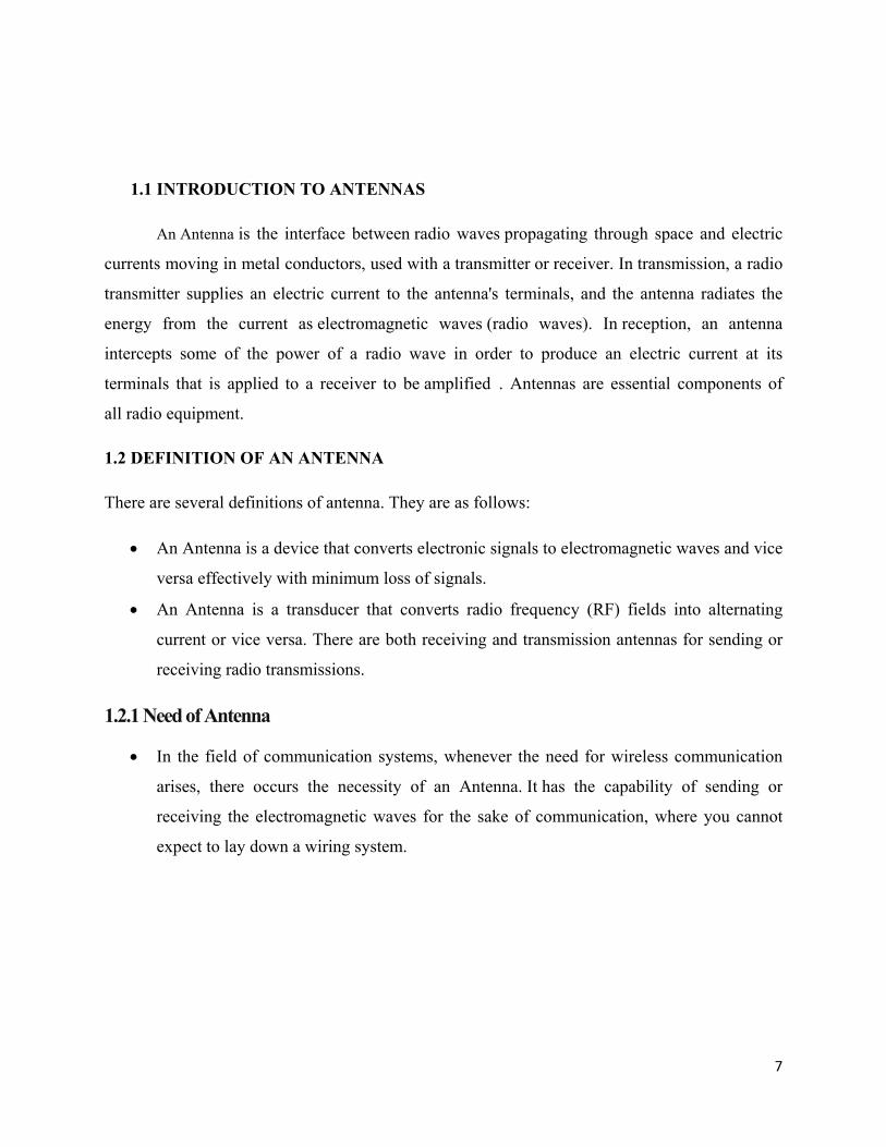
1.3 Equivalent circuit of antenna:
A Transmission-line Thevenin’s equivalent of the antenna system is shown in figure below. The transmission line is represented by a line with characteristics impedance Zs, and antenna is represented by a load ZL Where,
ZL =RL + jXL
Fig.1.1 transmission line model of antesnna
For high-frequency transmission lines, things behave quite differently. For instance, short-
circuits can actually have an infinite impedance; open-circuits can behave like short-circuited
wires. The impedance of some load (𝑍𝑍𝐿𝐿 = 𝑋𝑋𝐿𝐿 + 𝑗𝑗𝑌𝑌𝐿𝐿) can be transformed at the terminals of
the transmission line to an impedance much different than 𝑍𝑍𝐿𝐿.
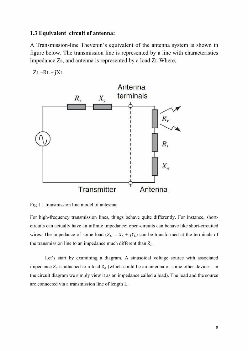
Let’s start by examining a diagram. A sinusoidal voltage source with associated
impedance 𝑍𝑍𝑆𝑆 is attached to a load 𝑍𝑍𝐴𝐴 (which could be an antenna or some other device – in
the circuit diagram we simply view it as an impedance called a load). The load and the source
are connected via a transmission line of length L.
9
Fig. 1.2 Transmission line model
In traditional low-frequency circuit analysis, the transmission line would not matter. As a
result, the current that flows in the circuit would simply be:
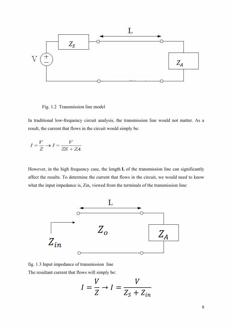
However, in the high frequency case, the length L of the transmission line can significantly
affect the results. To determine the current that flows in the circuit, we would need to know
what the input impedance is, Zin, viewed from the terminals of the transmission line:
fig. 1.3 Input impedance of transmission line
The resultant current that flows will simply be:
𝐼𝐼 =𝑉𝑉𝑍𝑍→ 𝐼𝐼 =
𝑉𝑉𝑍𝑍𝑆𝑆 + 𝑍𝑍𝑖𝑖𝑖𝑖
10
Since antennas are high-frequency devices (in the sense that their size is on the order of a half
wavlength or more), transmission line effects are often very important. That is, if the
length L of the transmission line significantly alters Zin, then the current into the antenna
from the source will be very small. Consequently, we will not be delivering power properly
to the antenna. The same problems hold true in the receiving mode: a transmission line can
skew impedance of the receiver sufficiently that almost no power is transferred from the
antenna.
Hence, a thorough understanding of antenna theory requires an understanding of transmission
lines. A great antenna can be hooked up to a great receiver, but if it is done with a length of
transmission line at high frequencies, the system will not work properly.
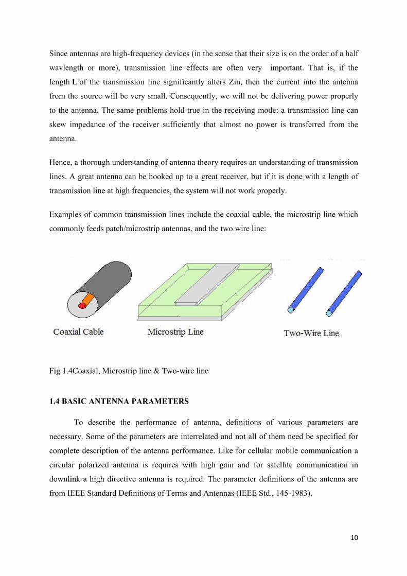
Examples of common transmission lines include the coaxial cable, the microstrip line which
commonly feeds patch/microstrip antennas, and the two wire line:
Fig 1.4Coaxial, Microstrip line & Two-wire line
1.4 BASIC ANTENNA PARAMETERS
To describe the performance of antenna, definitions of various parameters are
necessary. Some of the parameters are interrelated and not all of them need be specified for
complete description of the antenna performance. Like for cellular mobile communication a
circular polarized antenna is requires with high gain and for satellite communication in
downlink a high directive antenna is required. The parameter definitions of the antenna are
from IEEE Standard Definitions of Terms and Antennas (IEEE Std., 145-1983).
11
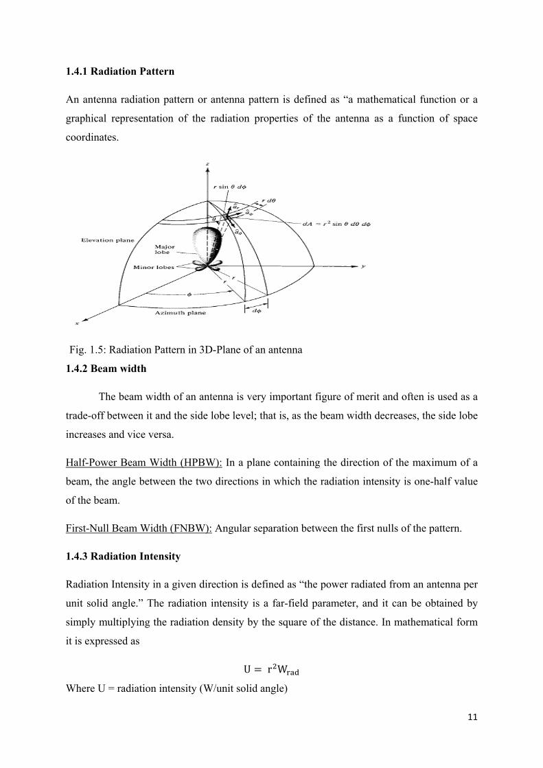
1.4.1 Radiation Pattern
An antenna radiation pattern or antenna pattern is defined as “a mathematical function or a
graphical representation of the radiation properties of the antenna as a function of space
coordinates.
Fig. 1.5: Radiation Pattern in 3D-Plane of an antenna
1.4.2 Beam width
The beam width of an antenna is very important figure of merit and often is used as a
trade-off between it and the side lobe level; that is, as the beam width decreases, the side lobe
increases and vice versa.
Half-Power Beam Width (HPBW): In a plane containing the direction of the maximum of a
beam, the angle between the two directions in which the radiation intensity is one-half value
of the beam.
First-Null Beam Width (FNBW): Angular separation between the first nulls of the pattern.
1.4.3 Radiation Intensity
Radiation Intensity in a given direction is defined as “the power radiated from an antenna per
unit solid angle.” The radiation intensity is a far-field parameter, and it can be obtained by
simply multiplying the radiation density by the square of the distance. In mathematical form
it is expressed as
U = r2Wrad
Where U = radiation intensity (W/unit solid angle)
12
𝑊𝑊𝑟𝑟𝑟𝑟𝑟𝑟 = radiation density (W/𝑚𝑚2)
1.4.4 Directivity
Directivity of an antenna shows that how much the antenna is able to radiate in a
particular given direction. The ratio of the radiation intensity in a given direction from the
antenna to the radiation intensity averaged over all directions.
Directivity = maximum radiation intensity
average radiation intensity
𝐷𝐷 = 𝑈𝑈𝑈𝑈0
=4𝜋𝜋𝑈𝑈𝑃𝑃𝑟𝑟𝑟𝑟𝑟𝑟
1.4.5 Return loss
Return loss is a measure of the effectiveness of power delivery from a transmission
line to a load such as an antenna. If the power incident on the antenna-under-test (AUT) is 𝑃𝑃𝑖𝑖𝑖𝑖
and the power reflected back to the source is 𝑃𝑃𝑟𝑟𝑟𝑟𝑟𝑟, then the return loss can be defined as
Return Loss = 10 log10 PinPref
dB
1.4.6 VSWR
VSWR describes how much energy is reflected from the antenna because of
impedance mismatching. A perfectly impedance antenna would have VSWR equal to one [1].
VSWR than 2:1(equivalent to a return loss of a -9.5dB) is considered to be acceptable for
most wireless applications because the time delay of any reflections is typically small, thus
providing small amounts of error within the receiver.
VSWR = 1 + Γ1 − Γ
Where, Γ is voltage reflection coefficient at the input terminals of the antenna.
1.4.7 Gain
Antenna Gain is also referred as Power gain or simply Gain. This combines of antenna
efficiency and directivity. For a transmitting antenna it shows how efficiently antenna is able
to radiate the given power into space in a particular direction. While in case of receiving
13
antenna it shows how well the antenna is to convert the received electromagnetic waves into
electrical power. When it is calculated with efficiency and directivity D it is referred as
Power Gain.
Power Gain = Eantenna. D
When the directivity with a particular direction is given it is known as Directive Gain.
Directive Gain (, ) =Eantenna. D (, )
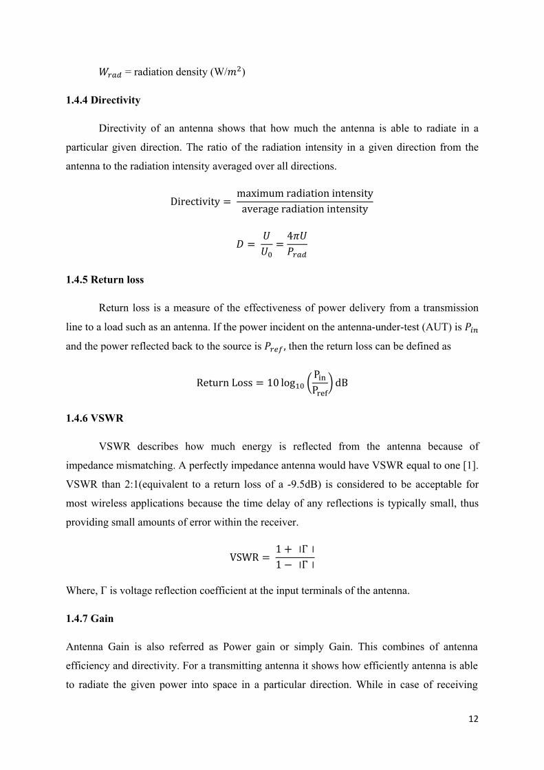
1.5 Radiation Pattern The energy radiated by an antenna is represented by the Radiation patternof the antenna. Radiation Patterns are diagrammatical representations of the distribution of radiated energy into space, as a function of direction.
Let us look at the pattern of energy radiation.
Fig 1.6 Radiation pattern of dipole antenna
14
The figure given above shows radiation pattern of a dipole antenna. The energy being radiated is represented by the patterns drawn in a particular direction. The arrows represent directions of radiation.
The radiation patterns can be field patterns or power patterns.
• The field patterns are plotted as a function of electric and magnetic fields. They are plotted on logarithmic scale.
• The power patterns are plotted as a function of square of the magnitude of electric and magnetic fields. They are plotted on logarithmic or commonly on dB scale.
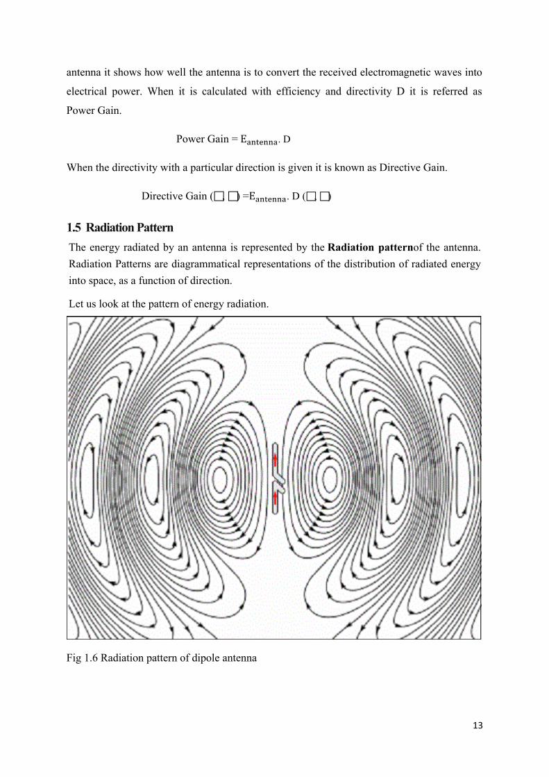
Radiation Pattern in 3D
The radiation pattern is a three-dimensional figure and represented in spherical coordinates (r, θ, Φ) assuming its origin at the center of spherical coordinate system. It looks like the following figure −
Fig 1.7 3D Radiation pattern
The given figure is a three dimensional radiation pattern for an Omni directional pattern. This clearly indicates the three co-ordinates (x, y, z).
Radiation Pattern in 2D
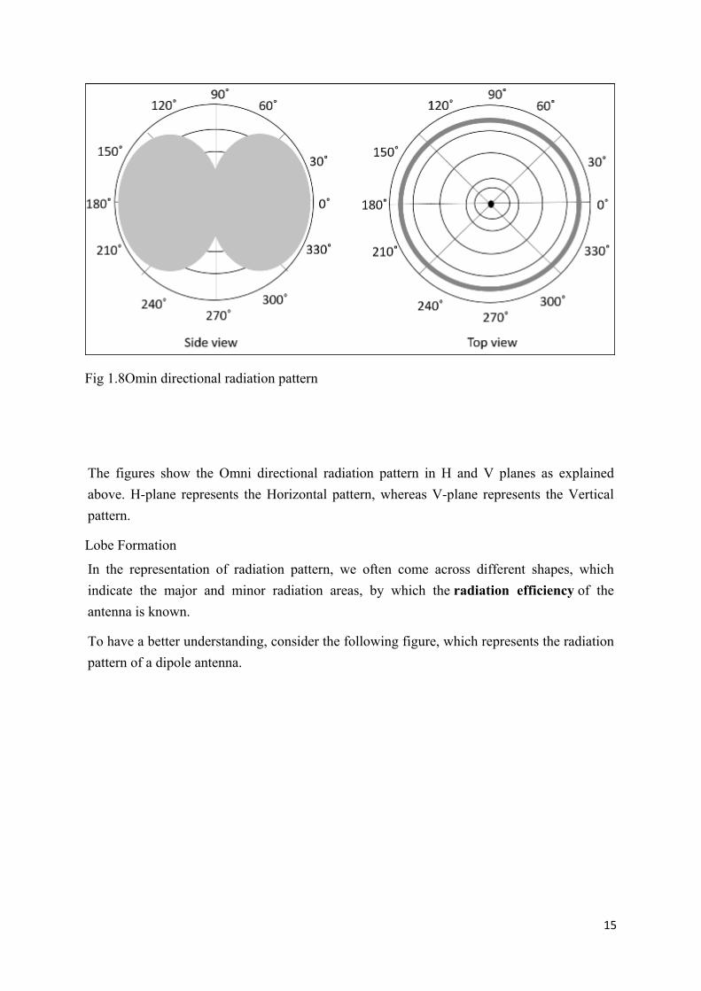
Two-dimensional pattern can be obtained from three-dimensional pattern by dividing it into horizontal and vertical planes. These resultant patterns are known as Horizontal pattern and Vertical pattern respectively.
15
Fig 1.8Omin directional radiation pattern
The figures show the Omni directional radiation pattern in H and V planes as explained above. H-plane represents the Horizontal pattern, whereas V-plane represents the Vertical pattern.
Lobe Formation
In the representation of radiation pattern, we often come across different shapes, which indicate the major and minor radiation areas, by which the radiation efficiency of the antenna is known.
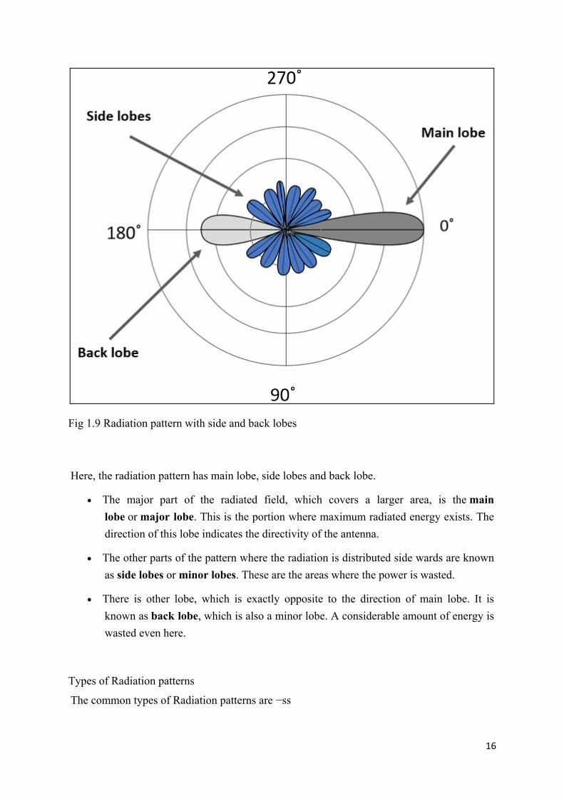
To have a better understanding, consider the following figure, which represents the radiation pattern of a dipole antenna.
16
Fig 1.9 Radiation pattern with side and back lobes
Here, the radiation pattern has main lobe, side lobes and back lobe.
• The major part of the radiated field, which covers a larger area, is the main lobe or major lobe. This is the portion where maximum radiated energy exists. The direction of this lobe indicates the directivity of the antenna.
• The other parts of the pattern where the radiation is distributed side wards are known as side lobes or minor lobes. These are the areas where the power is wasted.
• There is other lobe, which is exactly opposite to the direction of main lobe. It is known as back lobe, which is also a minor lobe. A considerable amount of energy is wasted even here.
Types of Radiation patterns
The common types of Radiation patterns are −ss
17
• Omni-directional pattern (also called non-directional pattern): The pattern usually has a doughnut shape in three-dimensional view. However, in two-dimensional view, it forms a figure-of-eight pattern.
• Pencil-beam pattern − The beam has a sharp directional pencil shaped pattern.
• Fan-beam pattern − The beam has a fan-shaped pattern.
• Shaped beam pattern − The beam, which is non-uniform and patternless is known as shaped beam.
A referential point for all these types of radiation is the isotropic radiation. It is important to
consider the isotropic radiation even though it is impractical.
1.6 TYPES OF ANTENNAS
We have different type of antennas. They are as follows:
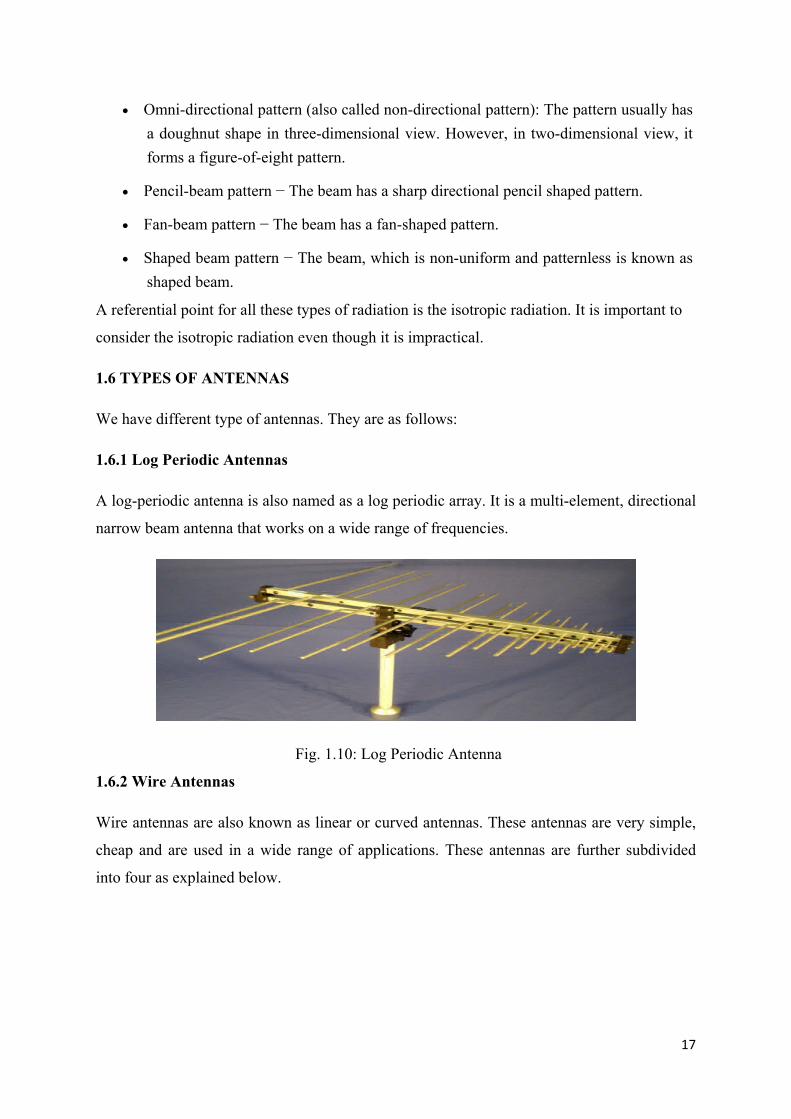
1.6.1 Log Periodic Antennas
A log-periodic antenna is also named as a log periodic array. It is a multi-element, directional
narrow beam antenna that works on a wide range of frequencies.
Fig. 1.10: Log Periodic Antenna
1.6.2 Wire Antennas
Wire antennas are also known as linear or curved antennas. These antennas are very simple,
cheap and are used in a wide range of applications. These antennas are further subdivided
into four as explained below.
18
Fig. 1.11: Wire Antenna
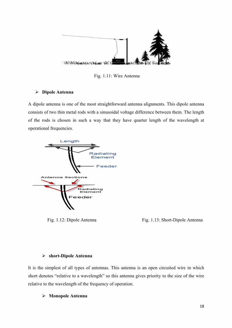
Dipole Antenna
A dipole antenna is one of the most straightforward antenna alignments. This dipole antenna
consists of two thin metal rods with a sinusoidal voltage difference between them. The length
of the rods is chosen in such a way that they have quarter length of the wavelength at
operational frequencies.
Fig. 1.12: Dipole Antenna Fig. 1.13: Short-Dipole Antenna
short-Dipole Antenna
It is the simplest of all types of antennas. This antenna is an open circuited wire in which
short denotes “relative to a wavelength” so this antenna gives priority to the size of the wire
relative to the wavelength of the frequency of operation.
Monopole Antenna
19
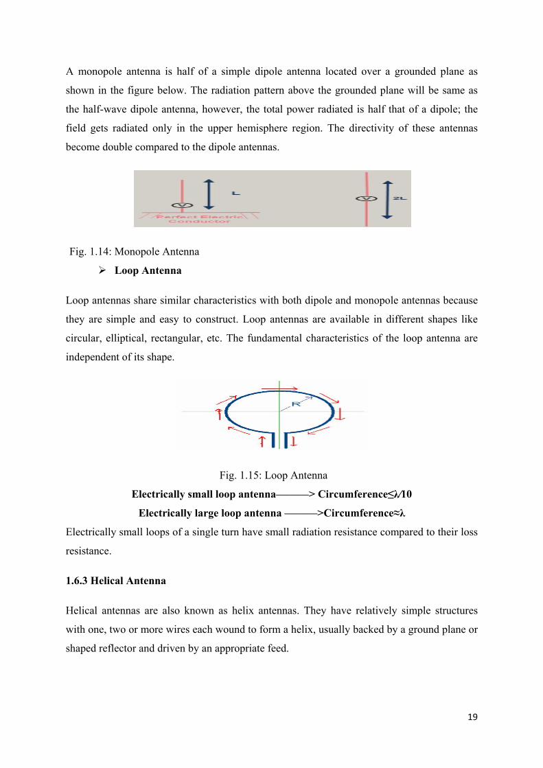
A monopole antenna is half of a simple dipole antenna located over a grounded plane as
shown in the figure below. The radiation pattern above the grounded plane will be same as
the half-wave dipole antenna, however, the total power radiated is half that of a dipole; the
field gets radiated only in the upper hemisphere region. The directivity of these antennas
become double compared to the dipole antennas.
Fig. 1.14: Monopole Antenna
Loop Antenna
Loop antennas share similar characteristics with both dipole and monopole antennas because
they are simple and easy to construct. Loop antennas are available in different shapes like
circular, elliptical, rectangular, etc. The fundamental characteristics of the loop antenna are
independent of its shape.
Fig. 1.15: Loop Antenna
Electrically small loop antenna———> Circumference≤λ⁄10
Electrically large loop antenna ———>Circumference≈λ
Electrically small loops of a single turn have small radiation resistance compared to their loss
resistance.
1.6.3 Helical Antenna
Helical antennas are also known as helix antennas. They have relatively simple structures
with one, two or more wires each wound to form a helix, usually backed by a ground plane or
shaped reflector and driven by an appropriate feed.
20
Fig. 1.16: Helical Antenna
1.6.4 Yagi-Uda Antenna
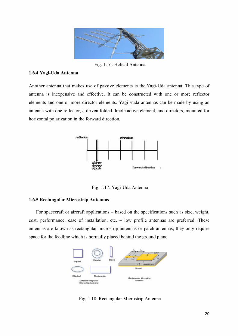
Another antenna that makes use of passive elements is the Yagi-Uda antenna. This type of
antenna is inexpensive and effective. It can be constructed with one or more reflector
elements and one or more director elements. Yagi vuda antennas can be made by using an
antenna with one reflector, a driven folded-dipole active element, and directors, mounted for
horizontal polarization in the forward direction.
Fig. 1.17: Yagi-Uda Antenna
1.6.5 Rectangular Microstrip Antennas
For spacecraft or aircraft applications – based on the specifications such as size, weight,
cost, performance, ease of installation, etc. – low profile antennas are preferred. These
antennas are known as rectangular microstrip antennas or patch antennas; they only require
space for the feedline which is normally placed behind the ground plane.
Fig. 1.18: Rectangular Microstrip Antenna
21
CHAPTER II MICROSTRIP PATCH ANTENNA
22
MICROSTRIP PATCH ANTENNA
Microstrip antenna was first introduced in the 1950s. this concept had to wait for about 20
years to be realized after the development of the printed circuit board (PCB) technology in
the 1970s. Since then, microstrip antennas are the most common types of antennas with wide
range of applications due to their apparent advantages of light weight, low profile, low cost,
planar configuration, easy of conformal, superior portability, suitable for array with the ease
of fabrication and integration with microwave monolithic integrate circuits (MMICs).They
have been widely engaged for the civilian and military applications such as radio-frequency
identification (RFID), broadcast radio, mobile systems, global positioning system (GPS),
television, multiple-input multiple-output (MIMO) systems, vehicle collision avoidance
system, satellite communications, surveillance systems, direction founding, radar systems,
remote sensing, missile guidance, and so on.
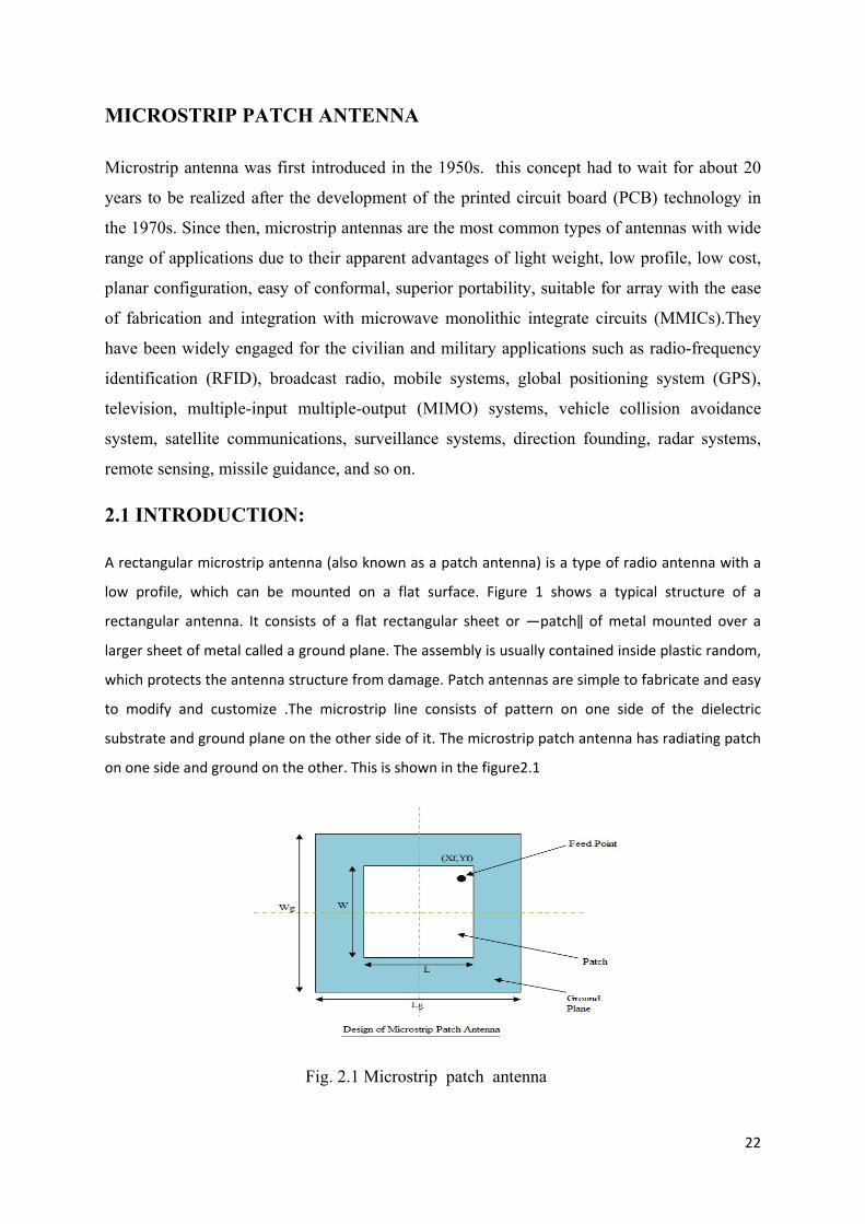
2.1 INTRODUCTION:
A rectangular microstrip antenna (also known as a patch antenna) is a type of radio antenna with a
low profile, which can be mounted on a flat surface. Figure 1 shows a typical structure of a
rectangular antenna. It consists of a flat rectangular sheet or ―patch‖ of metal mounted over a
larger sheet of metal called a ground plane. The assembly is usually contained inside plastic random,
which protects the antenna structure from damage. Patch antennas are simple to fabricate and easy
to modify and customize .The microstrip line consists of pattern on one side of the dielectric
substrate and ground plane on the other side of it. The microstrip patch antenna has radiating patch
on one side and ground on the other. This is shown in the figure2.1
Fig. 2.1 Microstrip patch antenna
23
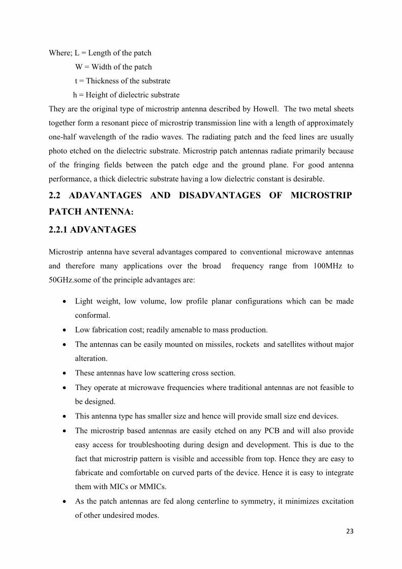
Where; L = Length of the patch
W = Width of the patch
t = Thickness of the substrate
h = Height of dielectric substrate
They are the original type of microstrip antenna described by Howell. The two metal sheets
together form a resonant piece of microstrip transmission line with a length of approximately
one-half wavelength of the radio waves. The radiating patch and the feed lines are usually
photo etched on the dielectric substrate. Microstrip patch antennas radiate primarily because
of the fringing fields between the patch edge and the ground plane. For good antenna
performance, a thick dielectric substrate having a low dielectric constant is desirable.
2.2 ADAVANTAGES AND DISADVANTAGES OF MICROSTRIP
PATCH ANTENNA:
2.2.1 ADVANTAGES
Microstrip antenna have several advantages compared to conventional microwave antennas
and therefore many applications over the broad frequency range from 100MHz to
50GHz.some of the principle advantages are:
• Light weight, low volume, low profile planar configurations which can be made
conformal.
• Low fabrication cost; readily amenable to mass production.
• The antennas can be easily mounted on missiles, rockets and satellites without major
alteration.
• These antennas have low scattering cross section.
• They operate at microwave frequencies where traditional antennas are not feasible to
be designed.
• This antenna type has smaller size and hence will provide small size end devices.
• The microstrip based antennas are easily etched on any PCB and will also provide
easy access for troubleshooting during design and development. This is due to the
fact that microstrip pattern is visible and accessible from top. Hence they are easy to
fabricate and comfortable on curved parts of the device. Hence it is easy to integrate
them with MICs or MMICs.
• As the patch antennas are fed along centerline to symmetry, it minimizes excitation
of other undesired modes.

24
• The microstrip patches of various shapes e.g. rectangular, square, triangular etc. are
easily etched.
• They have lower fabrication cost and hence they can be mass manufactured.
• They are capable of supporting multiple frequency bands (dual, triple).
• They support dual polarization types viz. linear and circular both.
• They are robust when mounted on rigid surfaces of the devices.
2.2.2 DISADVANTAGES:
Following are the disadvantages of Microstrip Antenna;
• The spurious radiation exists in various microstrip based antennas such as microstrip
patch antenna, microstrip slot antenna and printed dipole antenna.
• It offers low efficiency due to dielectric losses and conductor losses.
• It offers lower gain.
• It has higher level of cross polarization radiation.
• It has lower power handling capability.
• It has inherently lower impedance bandwidth.
• The microstrip antenna structure radiates from feeds and other junction points.
2.3 FEEDING TECHNIQUES
2.3.1 Inset Feed
Previously, the patch antenna was fed at the end as shown here. Since this typically yields a
high input impedance, we would like to modify the feed. Since the current is low at the ends
of a half-wave patch and increases in magnitude toward the center, the input impedance
(Z=V/I) could be reduced if the patch was fed closer to the center. One method of doing this
is by using an inset feed (a distance R from the end) as shown in Figure 2.2.
25
Fig. 2.2 Patch Antenna with an Inset Feed.
Since the current has a sinusoidal distribution, moving in a distance R from the end will
increase the current by cos(pi*R/L) - this is just noting that the wavelength is 2*L, and so the
phase difference is 2*pi*R/(2*L) = pi*R/L.
The voltage also decreases in magnitude by the same amount that the current increases.
Hence, using Z=V/I, the input impedance scales as:
In the above equation, Zin(0) is the input impedance if the patch was fed at the end. Hence,
by feeding the patch antenna as shown, the input impedance can be decreased. As an
example, if R=L/4, then cos(pi*R/L) = cos(pi/4), so that [cos(pi/4)]^2 = 1/2. Hence, a (1/8)-
wavelength inset would decrease the input impedance by 50%. This method can be used to
tune the input impedance to the desired value.
26
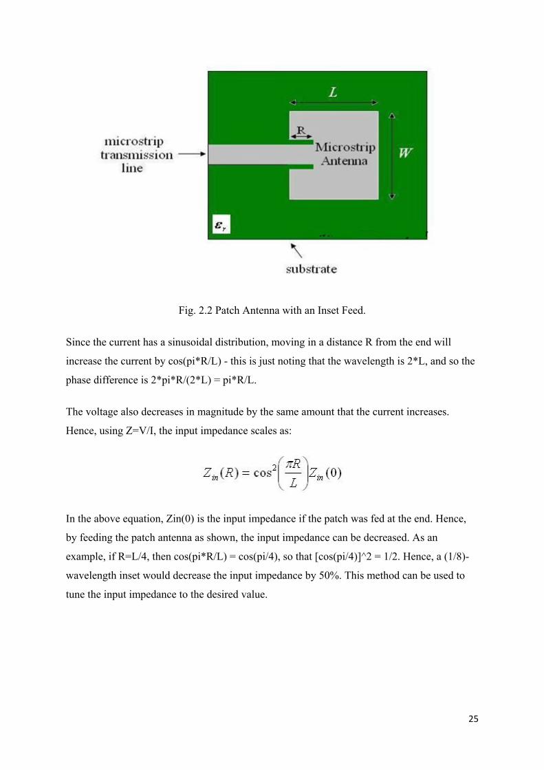
2.3.2 Feed with a Quarter-Wavelength Transmission Line
The microstrip antenna can also be matched to a transmission line of characteristic
impedance Z0 by using a quarter-wavelength transmission line of characteristic impedance
Z1 as shown in Figure 2.3.
Fig.2.3 Patch antenna with a quarter-wavelength matching section.
𝑍𝑍𝑖𝑖𝑖𝑖 = 𝑍𝑍0 =𝑍𝑍12
𝑍𝑍𝐴𝐴
This input impedance 𝑍𝑍𝑖𝑖𝑖𝑖can be altered by selection of the𝑍𝑍1, so that𝑍𝑍𝐼𝐼𝐼𝐼=𝑍𝑍0 and the antenna
is impedance matched. The parameter 𝑍𝑍1 can be altered by changing the width of the quarter-
wavelength strip. The wider the strip is, the lower the characteristic impedance (𝑍𝑍0) is for that
section of line.
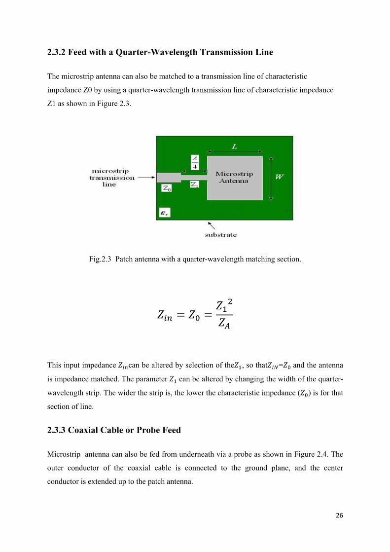
2.3.3 Coaxial Cable or Probe Feed
Microstrip antenna can also be fed from underneath via a probe as shown in Figure 2.4. The
outer conductor of the coaxial cable is connected to the ground plane, and the center
conductor is extended up to the patch antenna.
27
Fig. 2.4 Coaxial cable feed of patch antenna.
The position of the feed can be altered as before (in the same way as the inset feed, above) to
control the input impedance.
The coaxial feed introduces an inductance into the feed that may need to be taken into
account if the height h gets large (an appreciable fraction of a wavelength). In addition, the
probe will also radiate, which can lead to radiation in undesirable directions.
2.3.4 Coupled (Indirect) Feeds
The feeds above can be altered such that they do not directly touch the antenna. For instance,
the probe feed in Figure 3 can be trimmed such that it does not extend all the way up to the
antenna. The inset feed can also be stopped just before the patch antenna, as shown in Figure
2.5.
28
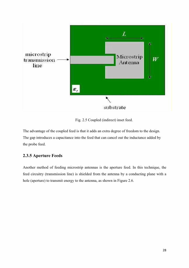
Fig. 2.5 Coupled (indirect) inset feed.
The advantage of the coupled feed is that it adds an extra degree of freedom to the design.
The gap introduces a capacitance into the feed that can cancel out the inductance added by
the probe feed.
2.3.5 Aperture Feeds
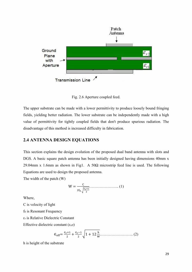
Another method of feeding microstrip antennas is the aperture feed. In this technique, the
feed circuitry (transmission line) is shielded from the antenna by a conducting plane with a
hole (aperture) to transmit energy to the antenna, as shown in Figure 2.6.
29
Fig. 2.6 Aperture coupled feed.
The upper substrate can be made with a lower permittivity to produce loosely bound fringing
fields, yielding better radiation. The lower substrate can be independently made with a high
value of permittivity for tightly coupled fields that don't produce spurious radiation. The
disadvantage of this method is increased difficulty in fabrication.
2.4 ANTENNA DESIGN EQUATIONS
This section explains the design evolution of the proposed dual band antenna with slots and
DGS. A basic square patch antenna has been initially designed having dimensions 40mm x
29.04mm x 1.6mm as shown in Fig1. A 50Ω microstrip feed line is used. The following
Equations are used to design the proposed antenna.
The width of the patch (W)
W = C
2f0 ∈r+12
………………….. (1)
Where,
C is velocity of light
f0 is Resonant Frequency
ԑr is Relative Dielectric Constant
Effective dielectric constant (ԑeff)
∈eff=∈r+12
+ ∈r−121 + 12 h
W…………………….. (2)
h is height of the substrate
30
Effective length (Leff)
Leff = C2f0∈eff
………………………… (3)
Length Extension (ΔL)
∆L = 0.412h(∈eff+0.3)(Wh+0.264)
(∈eff−0.258)(Wh+0.8)………………… (4)
Actual length of patch (L):
L = Leff − 2∆L………………………. (5)

31
CHAPTER 3
ULTRA-WIDEBAND ANTENNAS
32
3.1 INTRODUCTION OF UWB
An antenna is a transducer that converts guided electromagnetic energy in a transmission line
to radiated electromagnetic energy in free space. Antennas may also be viewed as an
impedance transformer, coupling between an input or line impedance, and the impedance of
free space.
The imminent widespread commercial deployment of ultra-wideband (UWB) systems has
sparked renewed interest in the subject of ultra-wideband antennas. The power levels
authorized by the FCC mean that every dB counts in a UWB system – as much or perhaps
even more so than in a standard narrowband system. Thus, an effective UWB antenna is a
critical part of an overall UWB system design.
UWB antennas have been in active commercial use for decades. In a sense, even the
venerable AM broadcast band antenna is “UWB” since it covers a band from 535- 1705 kHz
for a fractional bandwidth in excess of 100%. Because a high quality broadcast AM antenna
is really a tuned antenna designed to pick up an individual narrowband (10 kHz) channel, the
effective fractional bandwidth is really only 0.6-1.9% and only one channel can be received
at a time.
Starting in the early 1990s, the U.S. Army Research Laboratory (ARL) developed various
stationary and mobile ground-, foliage-, and wall-penetrating radar platforms that served to
detect and identify buried IEDs and hidden adversaries at a safe distance
3.2 UWB PRINTED WIDE SLOT ANTENNAS
The printed wide-slot antenna is another type of the most suitable candidates for UWB
applications. This type of antenna is commonly consists of a wide-slot and a tuning stub
connected with a microstrip or CPW feedline. Up to now, many wide-slot antennas, including
different wide-slots or tuning stubs, have been extensively studied on the antenna operation
bandwidth. Among various shapes of slot, the rectangular wide-slot is the simplest structure.
Based on the rectangular wide-slot, several shapes of the tuning stub are studied The antenna
bandwidth greatly depends on the length of the horizontal and vertical feed lines as well as on
the offset position of the feedline. The two slot antennas achieve the impedance bandwidth
ratios of 2.8:1 (1.7~ 4.9 GHz) and 3.5:1 (1.7~ 6.0 GHz), respectively. Yao et al. [proposed a
fan-shaped microstrip stub together with a strip, which contributes to a little wider with the
33
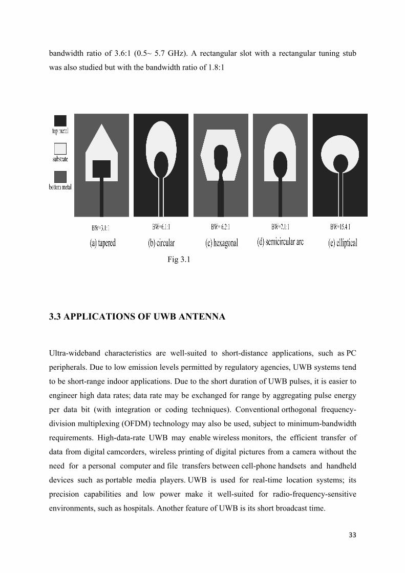
bandwidth ratio of 3.6:1 (0.5~ 5.7 GHz). A rectangular slot with a rectangular tuning stub
was also studied but with the bandwidth ratio of 1.8:1
Fig 3.1
3.3 APPLICATIONS OF UWB ANTENNA
Ultra-wideband characteristics are well-suited to short-distance applications, such as PC
peripherals. Due to low emission levels permitted by regulatory agencies, UWB systems tend
to be short-range indoor applications. Due to the short duration of UWB pulses, it is easier to
engineer high data rates; data rate may be exchanged for range by aggregating pulse energy
per data bit (with integration or coding techniques). Conventional orthogonal frequency-
division multiplexing (OFDM) technology may also be used, subject to minimum-bandwidth
requirements. High-data-rate UWB may enable wireless monitors, the efficient transfer of
data from digital camcorders, wireless printing of digital pictures from a camera without the
need for a personal computer and file transfers between cell-phone handsets and handheld
devices such as portable media players. UWB is used for real-time location systems; its
precision capabilities and low power make it well-suited for radio-frequency-sensitive
environments, such as hospitals. Another feature of UWB is its short broadcast time.
34
Ultra-wideband is also used in "see-through-the-wall" precision radar-imaging technology,
precision locating and tracking (using distance measurements between radios), and precision
time-of-arrival-based localization approaches. It is efficient, with a spatial capacity of
approximately 1013 bit/s/m². UWB radar has been proposed as the active sensor component
in an Automatic Target Recognition application, designed to detect humans or objects that
have fallen onto subway tracks.
In terms of military use, ultra-wideband gained widespread attention for its implementation
in synthetic aperture radar (SAR) technology. Due to how it retained high resolution despite
its use of lower frequencies, UWB SAR was heavily researched for its object-penetration
ability. . Examples include the railSAR, the boomSAR, the SIRE radar, and the SAFIRE
radar. ARL has also investigated the feasibility of whether UWB radar technology can
incorporate Doppler processing to estimate the velocity of a moving target when the platform
is stationary. While a 2013 report highlighted the issue with the use of UWB waveforms due
to target range migration during the integration interval, more recent studies have suggested
that UWB waveforms can demonstrate better performance compared to conventional Doppler
processing as long as a correct matched filter is used.
Ultra-wideband pulse Doppler radars have also been used to monitor vital signs of the human
body, such as heart rate and respiration signals as well as human gait analysis and fall
detection.
3.4 PROBLEM STATEMENT Ultra-Wide band antenna is designed with in the frequency band from (3.1-10.6GHZ). To
avoid the interference with existed narrow band military X band(7.25-7.745GHz), and
WLAN (5.15-5.725GHz) applications . A notch band is created in UWB antenna which
provides non resonance to the military X band, WLAN. Band rejection can be done by
inserting diodes to slots and its switching conditions.
35
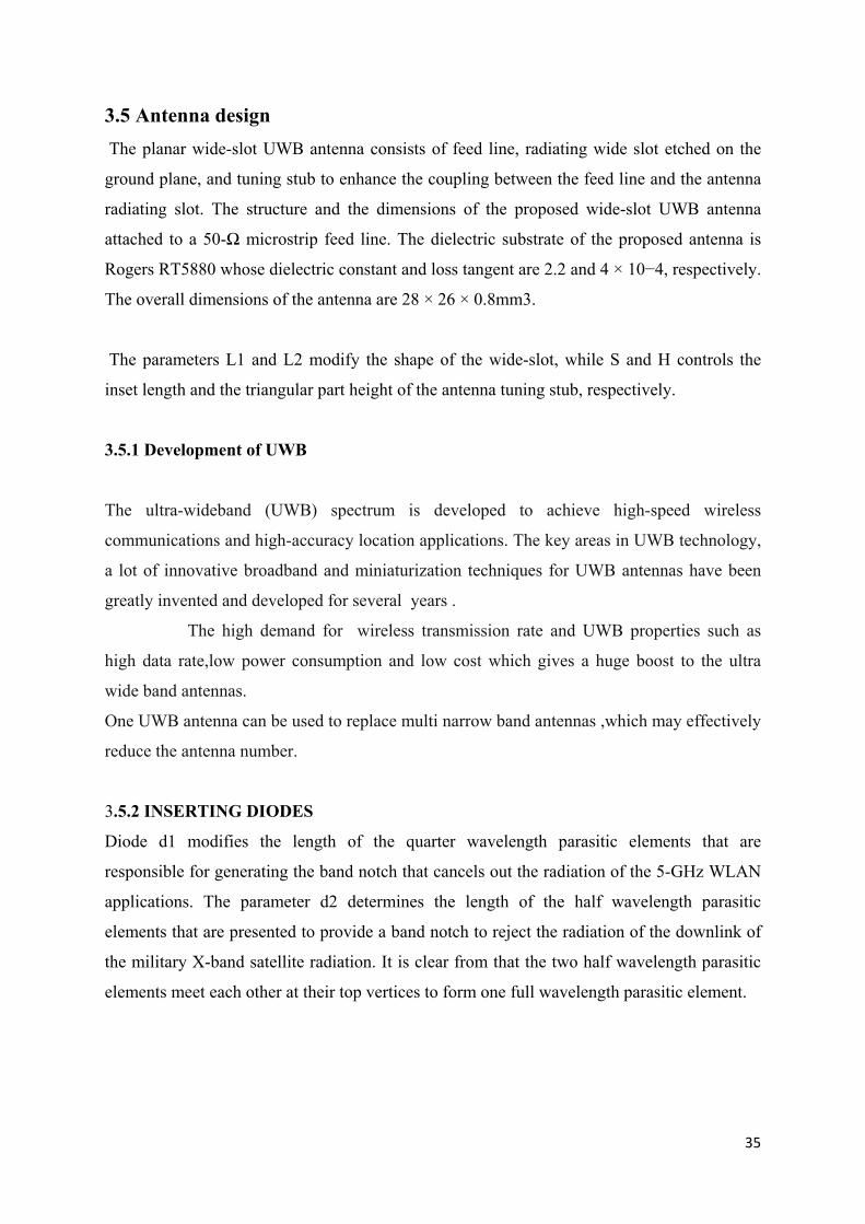
3.5 Antenna design The planar wide-slot UWB antenna consists of feed line, radiating wide slot etched on the
ground plane, and tuning stub to enhance the coupling between the feed line and the antenna
radiating slot. The structure and the dimensions of the proposed wide-slot UWB antenna
attached to a 50-Ω microstrip feed line. The dielectric substrate of the proposed antenna is
Rogers RT5880 whose dielectric constant and loss tangent are 2.2 and 4 × 10⁻⁴, respectively.
The overall dimensions of the antenna are 28 × 26 × 0.8mm3.
The parameters L1 and L2 modify the shape of the wide-slot, while S and H controls the
inset length and the triangular part height of the antenna tuning stub, respectively.
3.5.1 Development of UWB
The ultra-wideband (UWB) spectrum is developed to achieve high-speed wireless
communications and high-accuracy location applications. The key areas in UWB technology,
a lot of innovative broadband and miniaturization techniques for UWB antennas have been
greatly invented and developed for several years .
The high demand for wireless transmission rate and UWB properties such as
high data rate,low power consumption and low cost which gives a huge boost to the ultra
wide band antennas.
One UWB antenna can be used to replace multi narrow band antennas ,which may effectively
reduce the antenna number.
3.5.2 INSERTING DIODES
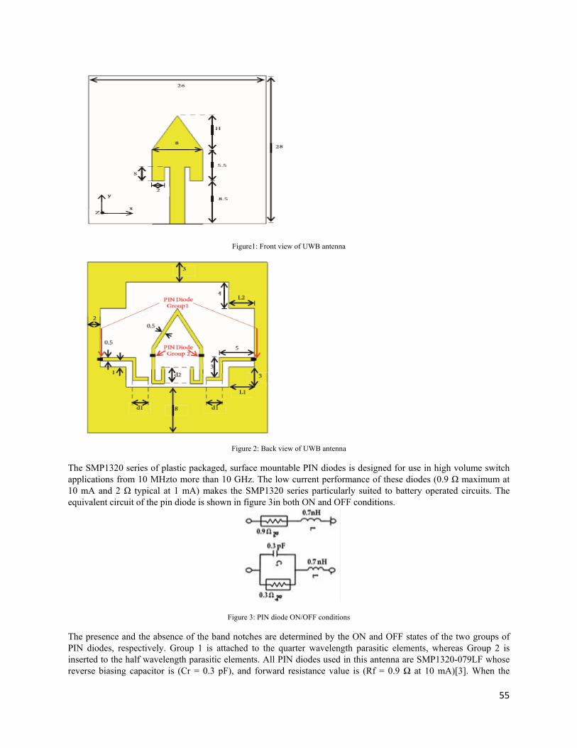
Diode d1 modifies the length of the quarter wavelength parasitic elements that are
responsible for generating the band notch that cancels out the radiation of the 5-GHz WLAN
applications. The parameter d2 determines the length of the half wavelength parasitic
elements that are presented to provide a band notch to reject the radiation of the downlink of
the military X-band satellite radiation. It is clear from that the two half wavelength parasitic
elements meet each other at their top vertices to form one full wavelength parasitic element.
36
Fig 3.2 patch
Fig 3.3 Ground
The presence and the absence of the band notches are determined by the ON and OFF states
of the two groups of PIN diodes, respectively. Group 1 is attached to the quarter wavelength
parasitic elements, whereas Group 2 is inserted to the half wavelength parasitic elements. All
PIN diodes used in this antenna are SMP1320-079LF whose reverse biasing capacitor is (Cr
= 0.3 pF), and forward resistance value is (Rf = 0.9 Ω at 10 mA). It is worth mentioning that
the OFF and ON states of the PIN diodes are simulated by the reverse biasing capacitance
and the forward biasing resistance, respectively, during the antenna simulation process.
3.5.3 DIODE SWITCHING CONDITIONS

37
DIODE ON CONDITION: In diode ON condition the inductor is in series with parallel
combination of resistance and capacitance
DIODE ON CONDITION: In diode OFF condition condition the inductor is in series with
capacitance

38
CHAPTER 4
HFSS

39
4.1 OVERVIEW HFSS is a high-performance full-wave electromagnetic field simulator for arbitrary 3D
volumetric passive device modeling that takes advantage of the familiar Microsoft Windows
graphical user interface. It integrates simulation, visualization, solid modeling, and
automation in an easy-to-learn environment.
HFSS includes:
1. A graphical interface to simplify design entry
2. A field solving engine with accuracy-driven adaptive solutions
3. Powerful post processor for displaying currents, fields and RF parameters
4. Automatic and adaptive mesh generation and refinement and tangential vector finite
elements
5. Macro feature allows for users to log sessions of design or simulation to an easy to
read file (useful in creating a library of structure based on a nominal structure)
6. A comprehensive materials database that contains permittivity-, permeability, electric-
, magnetic-loss tangents for common materials.
Typical HFSS Uses
1. PCB Board Modeling: Power and Ground Planes, Backplanes
2. EMC/EMI: Shield Enclosures, Coupling, Near- and Far- Radiation
3. Antennas/Mobile Communications: Patches, Horns, Radar Cross Section
4. Connectors: Coaxial (Coax), Transitions
5. Waveguide: Filters, Resonators, Transitions, Couplers
4.1.2 DESIGNING USING HFSS
Set up the Design
– Launch Ansoft HFSS, Set the Tool Option, Rename the open a New Project
Launch Ansoft HFSS
• To access Ansoft HFSS,click the Microsoft Startbutton, select Programs ,and select the Ansoft>HFSS 10 program group. Click HFSS 10. Setting Tool Options

40
• Select the menu item Tools>Options>HFSS Options
• HFSS Options Window: o Click the General Tab
Use wizards for data entry when creating new boundaries: Checked
Duplicate boundaries with geometry :Checked o Click the OK button
• Select the menu item Tools>Options>3D Modeler Options • 3D Modeler Options Window
o Click the Operation tab Automatically cover closed polylines:Checked
o Click the Drawing tab Edit property of new primitives:Checked
Click the OK
Save a New Project
• Click File>SaveAs • Use the file browser to locate the folder in which you want to save
the project andthen double click the folder’sname • Type Antenna and File Name text box and then clickSave. • Do not forget to save your design periodically throughout the design.
Create the 3-D model
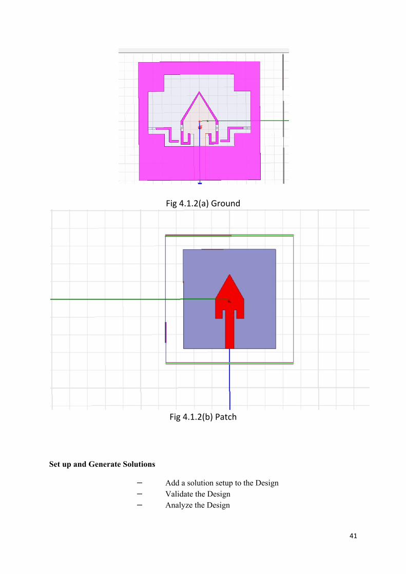
• Set the default material • Create Substrate • Create Infinite Ground • Assign boundary condition • Create conductor patches • Create Wave ports and Excitations • Set up the Radiation Boundary
41
Fig 4.1.2(a) Ground
Fig 4.1.2(b) Patch
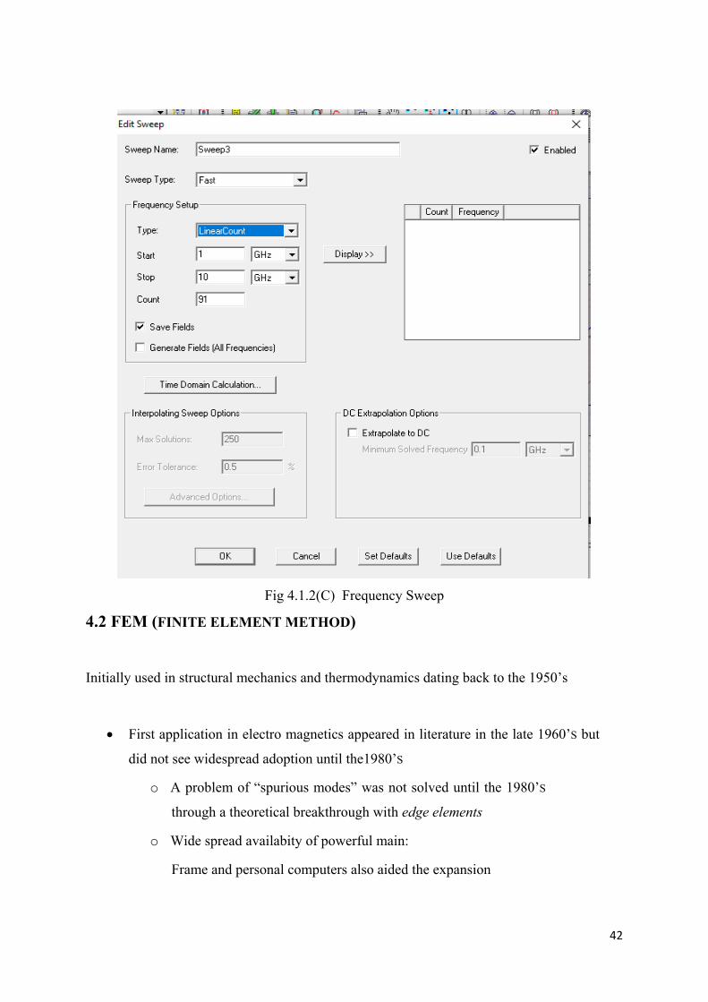
Set up and Generate Solutions
– Add a solution setup to the Design – Validate the Design – Analyze the Design
42
Fig 4.1.2(C) Frequency Sweep
4.2 FEM (FINITE ELEMENT METHOD)
Initially used in structural mechanics and thermodynamics dating back to the 1950’s
• First application in electro magnetics appeared in literature in the late 1960’S but
did not see widespread adoption until the1980’S
o A problem of “spurious modes” was not solved until the 1980’S
through a theoretical breakthrough with edge elements
o Wide spread availabity of powerful main:
Frame and personal computers also aided the expansion

43
Starts with the partial differential equation (PDE) form of Maxwell’s Equations
• Solution can be viewed from two main perspectives
o Variation analysis
Finds a variational functional whose minimum corresponds to the
solution of the PDE
o Weighted residuals
Introducesa“weighted”residualorerrorandusingGreen’sfunction,sh
iftoneofthe differentials in the PDE to the weighting functions
o In most applications these two viewpoints result in identical equations
• FEM can handle essentially two different types of EM problems
o Eigen analysis (source-free)
o Deterministic (driven)
• FEM does not include a radiation condition
o Open regions, such as antennas (see below), requires special treatment
Introduction of a artificial absorbing region within the mesh
Strengths • Handles complex geometries and material in homogeneities easily
• Handles dispersive or frequency-dependent materials easily
• Handles Eigen problems easily
• Has better frequency scaling characteristics that MOM (but usually requires a larger
set of unknowns)
• Easily applicable to “multi-physics” problems by coupling solutions in thermal or
mechanical to the EM solution
Weaknesses • Inefficient treatment of highly conducting radiators when compared to the MoM
• FEM meshes become very complex for large 3-D structures
• More difficult to implement than the FDTD thus limiting their use in commercial
software. Little code development is done by engineers
• Efficient preconditioned iterative solvers are required when higher-order elements are
used. Again, restricting the code development by individual engineers
44
Some Companies that market commercial FEM EM software: • Ansoft Corporation, Inc.
– High frequency structure simulator (HFSS)
• Ansys, Inc.
– Emag
• Comsol, Inc.
– COMSOL Multi physics with Electro magnetics Module
• Solid Works Corporation
– COSMOSEMS
4.3 DESIGN PROCEDURE
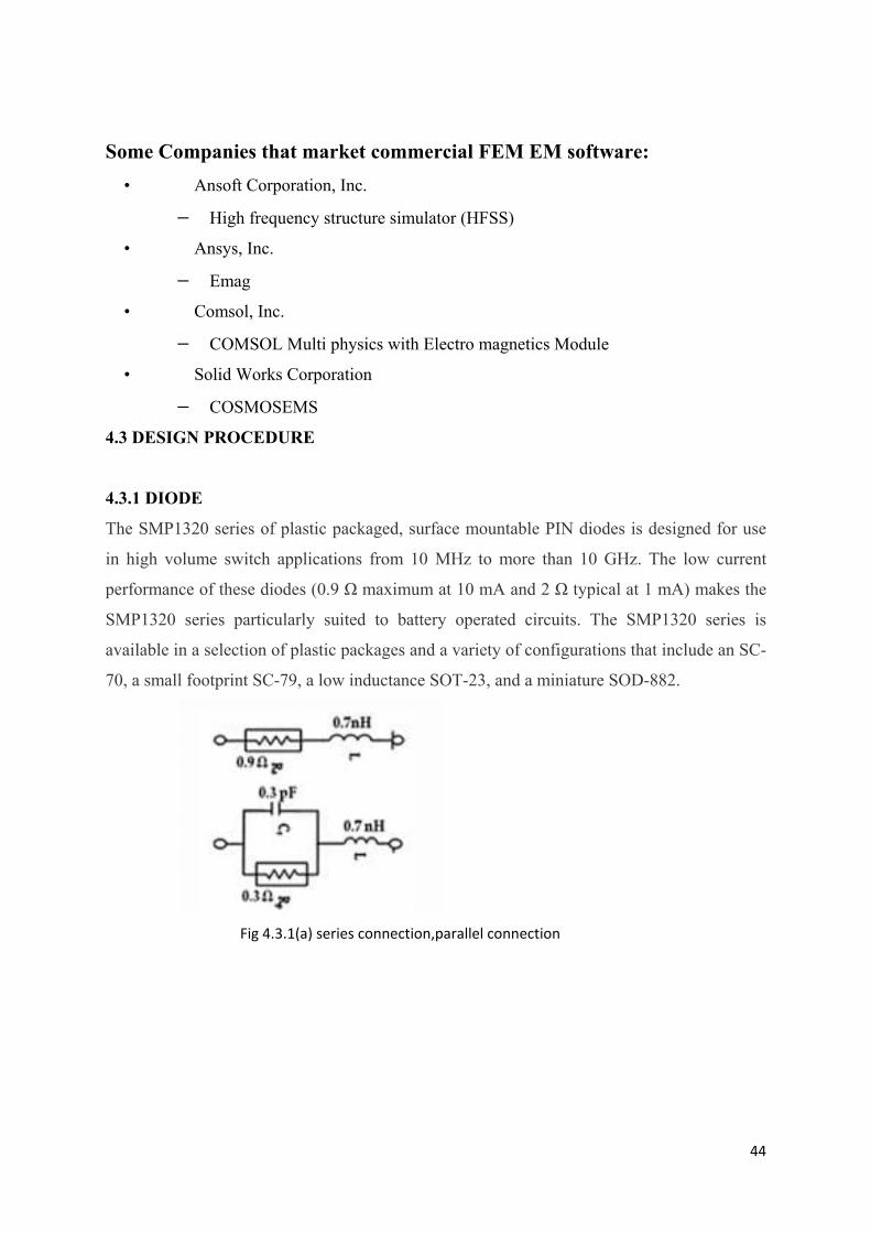
4.3.1 DIODE
The SMP1320 series of plastic packaged, surface mountable PIN diodes is designed for use
in high volume switch applications from 10 MHz to more than 10 GHz. The low current
performance of these diodes (0.9 Ω maximum at 10 mA and 2 Ω typical at 1 mA) makes the
SMP1320 series particularly suited to battery operated circuits. The SMP1320 series is
available in a selection of plastic packages and a variety of configurations that include an SC-
70, a small footprint SC-79, a low inductance SOT-23, and a miniature SOD-882.
Fig 4.3.1(a) series connection,parallel connection
45
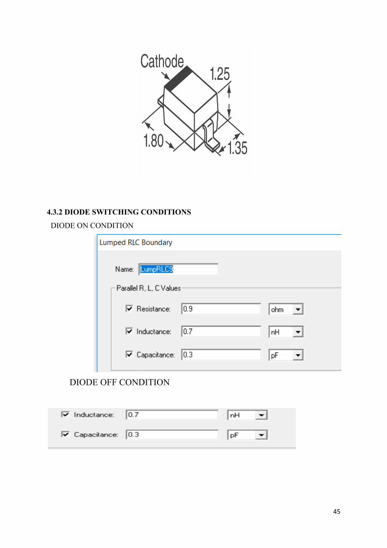
4.3.2 DIODE SWITCHING CONDITIONS
DIODE ON CONDITION
DIODE OFF CONDITION

46
CHAPTER 5
RESULTS
47
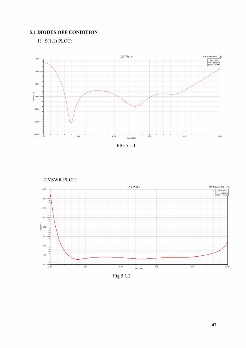
5.1 DIODES OFF CONDITION
1) S(1,1) PLOT:
FIG 5.1.1
2)VSWR PLOT:
Fig 5.1.2
2.00 4.00 6.00 8.00 10.00 12.00Freq [GHz]
-30.00
-25.00
-20.00
-15.00
-10.00
-5.00
0.00
dB(S
(1,1
))
UWB diodes OFFXY Plot 4 ANSOFT
Curve InfodB(S(1,1))
Setup1 : Sw eep
2.00 4.00 6.00 8.00 10.00 12.00Freq [GHz]
0.00
2.00
4.00
6.00
8.00
10.00
12.00
14.00
16.00
VSW
R(1
)
UWB diodes OFFXY Plot 5 ANSOFT
Curve InfoVSWR(1)
Setup1 : Sw eep
48
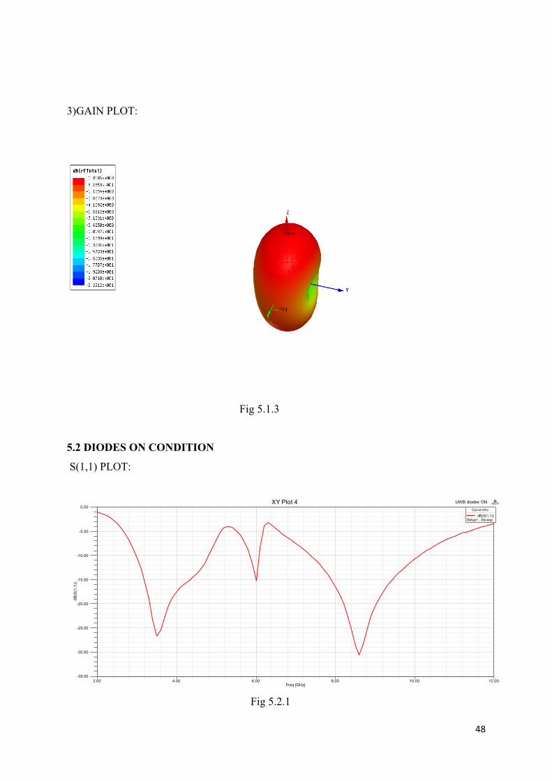
3)GAIN PLOT:
Fig 5.1.3
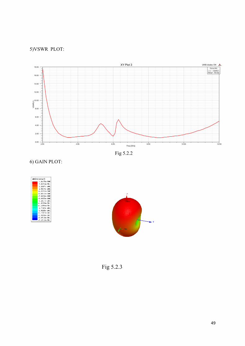
5.2 DIODES ON CONDITION
S(1,1) PLOT:
Fig 5.2.1
2.00 4.00 6.00 8.00 10.00 12.00Freq [GHz]
-35.00
-30.00
-25.00
-20.00
-15.00
-10.00
-5.00
0.00
dB(S
(1,1
))
UWB diodes ONXY Plot 4 ANSOFT
Curve InfodB(S(1,1))
Setup1 : Sw eep
49
5)VSWR PLOT:
Fig 5.2.2
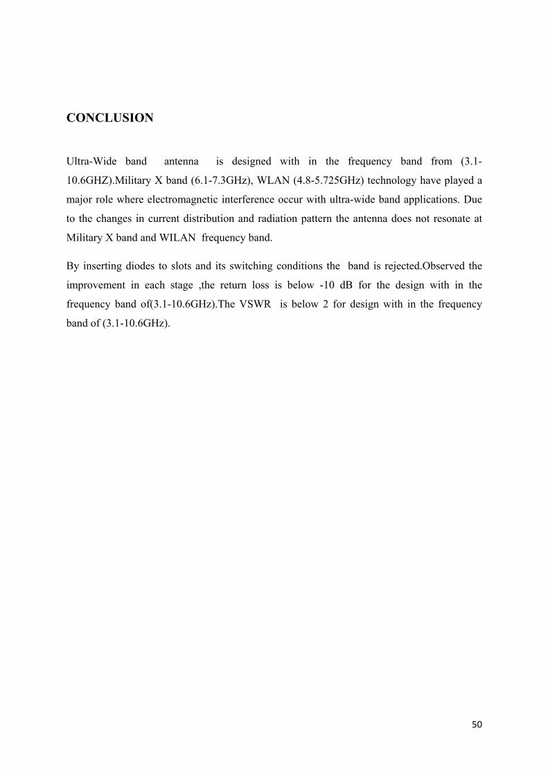
6) GAIN PLOT:
Fig 5.2.3
2.00 4.00 6.00 8.00 10.00 12.00Freq [GHz]
0.00
2.00
4.00
6.00
8.00
10.00
12.00
14.00
16.00
18.00
VSW
R(1
)
UWB diodes ONXY Plot 3 ANSOFT
Curve InfoVSWR(1)
Setup1 : Sw eep
50
CONCLUSION
Ultra-Wide band antenna is designed with in the frequency band from (3.1-
10.6GHZ).Military X band (6.1-7.3GHz), WLAN (4.8-5.725GHz) technology have played a
major role where electromagnetic interference occur with ultra-wide band applications. Due
to the changes in current distribution and radiation pattern the antenna does not resonate at
Military X band and WILAN frequency band.
By inserting diodes to slots and its switching conditions the band is rejected.Observed the
improvement in each stage ,the return loss is below -10 dB for the design with in the
frequency band of(3.1-10.6GHz).The VSWR is below 2 for design with in the frequency
band of (3.1-10.6GHz).
51
REFERENCES
[1]A Novel Printed UWB Slot Antenna With Reconfigurable Band-Notch
Characteristics Nasrin Tasouji, Javad Nourinia, Member, IEEE, Changiz Ghobadi, and
Farzad Tofigh, Student Member, IEEE
[2] A. Valizade, Ch. Ghobadi, J. Nourinia, and M. Ojaroudi. “A Novel Design of
Reconfigurable Slot Antenna With Switchable Band Notch and Multiresonance
Functions forUWBApplications”,IEEE Antennas and wireless propagation
letters,VOL.12,2013 Page(s): 1166 - 1169, October 2012
[3] Nasrin Tasouji, Javad Nourinia, Member, IEEE, Changiz Ghobadi, and Farzad
Tofigh, “A Novel Printed UWB Slot Antenna With Reconfigurable Band-Notch
Characteristics”. IEEE Antennas and wireless propagation letter IEEE. Page(s): 922 -
925, July 2013
[4]Bahareh Badamchi1, Javad Nourinia1, Changiz Ghobadi1, Arash Valizade
Shahmirzadi “Design of compact reconfigurable ultra-wideband slot antenna with
switchable single/dual band notch functions.” IET Microw. Antennas Propag.
Page(s): 541 - 548.June 2014
[5] Chao-Ming Luo, Jing-Song Hong, Muhammad Amin, and Lei Zhong School of
Physical Electronics,“Compact UWB Antenna with Triple Notched Bands
Reconfigurable” .Electronics letters.June 2016
[6] Anudeepa S. Kholapure1 and R.G. Karandikar2. ,”Antenna with reconfigurable
triple band notched characteristics for cognitive radio.” ICTACT Journal on
communication technology ,2016
[7] K. V. Ajetrao A. P. Dhande, “Phi Shape UWB Antenna with Band Notch
Characteristics.”, Engineering, Technology & Applied Science Research
Vol. 8, No. 4, 2018
[8] Saeed Ur Rahman | Qunsheng Cao | Yi Wang | Habib Ullah. , “Design of wideband
antenna with band notch characteristics based on single notching element” ,Int Journal
RF Microwave Computer Aided Eng, October 2018

52
[9] Amir H. Nazeri, A. Falahati, R.M. Edwards, “A Novel Compact Fractal UWB
Antenna with Triple Reconfigurable Notch Reject Bands Applications” International
Journal of Electronics and Communications , January 2019
Ultra Wide Band Antenna with Band Rejection Configurability for Wireless Applications
2
Abstract-: The design of Ultra Wide band antenna is suitable for short range with high data speed in wireless
applications within the frequency band from (3.1-10.6GHZ). Ultra-Wide band applications can coexist with other narrow band communications standards that occupy the same spectrum .Military X band (7.25-7.745GHz), WLAN (5.15-5.725GHz) technology have played a major role where electromagnetic interference occur with ultra-wide band applications. While designing an antenna, improvement in the antenna characteristics is a major demand of the wireless industry that is growing rapidly. Microstrip antennas are used in extensive range of applications such as wireless and biomedical diagnosis. A microstrip antenna quite has a lot of advantages over the other antennas due to their light weight, robustness, low cost of production and low profile nature. In this proposed project work, the simple rectangular patch antenna with line feed is used .To avoid the interference with existed narrow band military X band and WLAN applications, the UWB antenna with band notch characteristics is required. A notch band is created in UWB antenna which provides non resonance to the military X band, WLAN. Band rejection can be done by inserting diodes to slots and its switching conditions. The antenna size can be reduced which achieves the miniaturization of antenna size, material cost and helpful in portability that can be used in wide range of applications. ANSYS HFSS is used to analyze and design this antenna. Index Terms- Band notch, Interference, ultra wide band.
1. INTRODUCTION Due to the enormous deployment of wireless communication systems, the frequency spectrum allocation has witnessed a noticeable congestion in the last few decades. This serious issue has restricted the response to the incredible customers’ demand for new forms of high-performance communication systems. Cognitive radio (CR) [1] systems were invented to mitigate the limitations of the frequency spectrum allocation. As identified by the Federal Communication Commission (FCC) [2], about 70% of the allocated spectrum is idle for a remarkable amount of time. CR systems recruit the idle frequency, which is specified for a licensed user (primary user), for another unlicensed user (secondary user). In other words, the secondary user can communicate via the primary user’s channel as long as the primary user is in its idle mode. CR systems are divided into interweave and underlay systems. The former category of CR systems uses an ultrawide-band (UWB) antenna to sense the presence of the idle channels and another reconfigurable antenna [3] for communication purposes . On the other hand, the underlay CR systems, which represent the main scope of this work, utilize a single UWB antenna with reconfigurable band notches [4] to cancel the communication via the licensed channels during the active modes of the primary users. The underlay CR systems transmit a reduced amount of power along the UWB frequency band (3.1–10.6 GHz) [5] to minimize the interference with the already existing applications. Some applications do not accept any amount of interference, so the UWB antenna of the underlay systems should have the capability of band notch generation to completely eliminate the interference with these critical applications. Like the conventional frequency reconfiguration [6], the reconfiguration of the antenna band notch may be accomplished with the aid of radio frequency (RF) switches such as PIN diodes [7], MEMS switches, and photoconductive switches. In addition, the band notch center frequency can be tuned by attaching a varactor diode to the designed antenna. For planar monopole UWB antennas [8], reconfigurable band notches can be presented in many ways such as controlling the length of a slot etched on the ground plane, modifying the length of parasitic elements, or reshaping split ring
Ms. M. Nirmala Mr.S.Riyaz Basha Mr.V.Sai Sandeep Assistant Professor UG Student UG Student ANITS Visakhapatnam ANITS Visakhapatnam ANITS Visakhapatnam [email protected] [email protected] [email protected]
Ms. K.Ratnavathi Mr.B.Suresh UG Student UG Student ANITS Visakhapatnam ANITS Visakhapatnam [email protected] [email protected]
54
resonators. However, the band notch reconfiguration of wide-slot UWB antennas may be achieved by controlling the length of slots etched on the antenna tuning stubs, attaching a variable length parasitic element to the radiating stub , or modifying the length of parasitic elements attached to the tuning stub . A compact wide-slot UWB antenna with two sharp and reconfigurable band notches for underlay CR communications is proposed in this paper. The shapes of the slot and the tuning stub of the proposed antenna are modified so that the antenna operating bandwidth covers the entire UWB frequency spectrum (3.1–10.6 GHz). The two band notches are generated by presenting two parasitic elements within the antenna slot. The first band notch is generated by inserting a pair of quarter wavelength parasitic elements to the ground plane to reject the radiation of the 5GHz WLAN (5.15–5.725 GHz). A pair of half wavelength parasitic elements is engraved on the ground plane side of the antenna along the circumference of the antenna tuning stub to avoid the interference with the down link of the military X-band satellite communications (7.25–7.745 GHz). Each band notch is switched ON and OFF by a pair of PIN diodes. The measurements agree well with the simulated results and both verify the sharpness and successful reconfiguration of the two band notches.
2. ANTENNA DESIGN CONFIGURATION
This section explains the design evolution of the proposed dual band antenna with slots and DGS. A basic square patch antenna has been initially designed having dimensions 40mm x 29.04mm x 1.6mm as shown A 50Ω microstrip feed line is used. The following Equations are used to design the proposed antenna. The width of the patch (W) W = C
2f0 ∈r+12
………………………………………. (1)
Where, C is velocity of light f0 is Resonant Frequency εr is Relative Dielectric Constant Effective dielectric constant ԑeff is
∈eff=∈r+12
+ ∈r−121 + 12 h
W……………………. (2)
h is height of the substrate Effective length Leff is Leff = C
2f0∈eff………………………………………... (3)
Length Extension ΔL is
∆L = 0.412h(∈eff+0.3)(Wh+0.264)
(∈eff−0.258)(Wh+0.8)………………….. (4)
Actual length of patch L is L = Leff − 2∆L……………………………………… (5) The planar wide-slot UWB antenna consists of feed line, radiating wide slot etched on the ground plane, and tuning stub to enhance the coupling between the feed line and the antenna radiating slot. The structure and the dimensions of the proposed wide-slot UWB antenna attached to a 50-Ω microstrip feed line. The dielectric substrate of the proposed antenna is Rogers RT5880 whose dielectric constant and loss tangent are 2.2 and 4 × 10⁻⁴, respectively. The overall dimensions of the antenna are 28 × 26 × 0.8mm. The antenna layouts are shown in Figure 1 and Figure 2. Diode d1 modifies the length of the quarter wavelength parasitic elements that are responsible for generating the band notch that cancels out the radiation of the 5-GHz WLAN applications. The parameter d2 determines the length of the half wavelength parasitic elements that are presented to provide a band notch to reject the radiation of the downlink of the military X-band satellite radiation. It is clear from that the two half wavelength parasitic elements meet each other at their top vertices to form one full wavelength parasitic element.
55
Figure1: Front view of UWB antenna
Figure 2: Back view of UWB antenna
The SMP1320 series of plastic packaged, surface mountable PIN diodes is designed for use in high volume switch applications from 10 MHzto more than 10 GHz. The low current performance of these diodes (0.9 Ω maximum at 10 mA and 2 Ω typical at 1 mA) makes the SMP1320 series particularly suited to battery operated circuits. The equivalent circuit of the pin diode is shown in figure 3in both ON and OFF conditions.
Figure 3: PIN diode ON/OFF conditions
The presence and the absence of the band notches are determined by the ON and OFF states of the two groups of PIN diodes, respectively. Group 1 is attached to the quarter wavelength parasitic elements, whereas Group 2 is inserted to the half wavelength parasitic elements. All PIN diodes used in this antenna are SMP1320-079LF whose reverse biasing capacitor is (Cr = 0.3 pF), and forward resistance value is (Rf = 0.9 Ω at 10 mA)[3]. When the
56
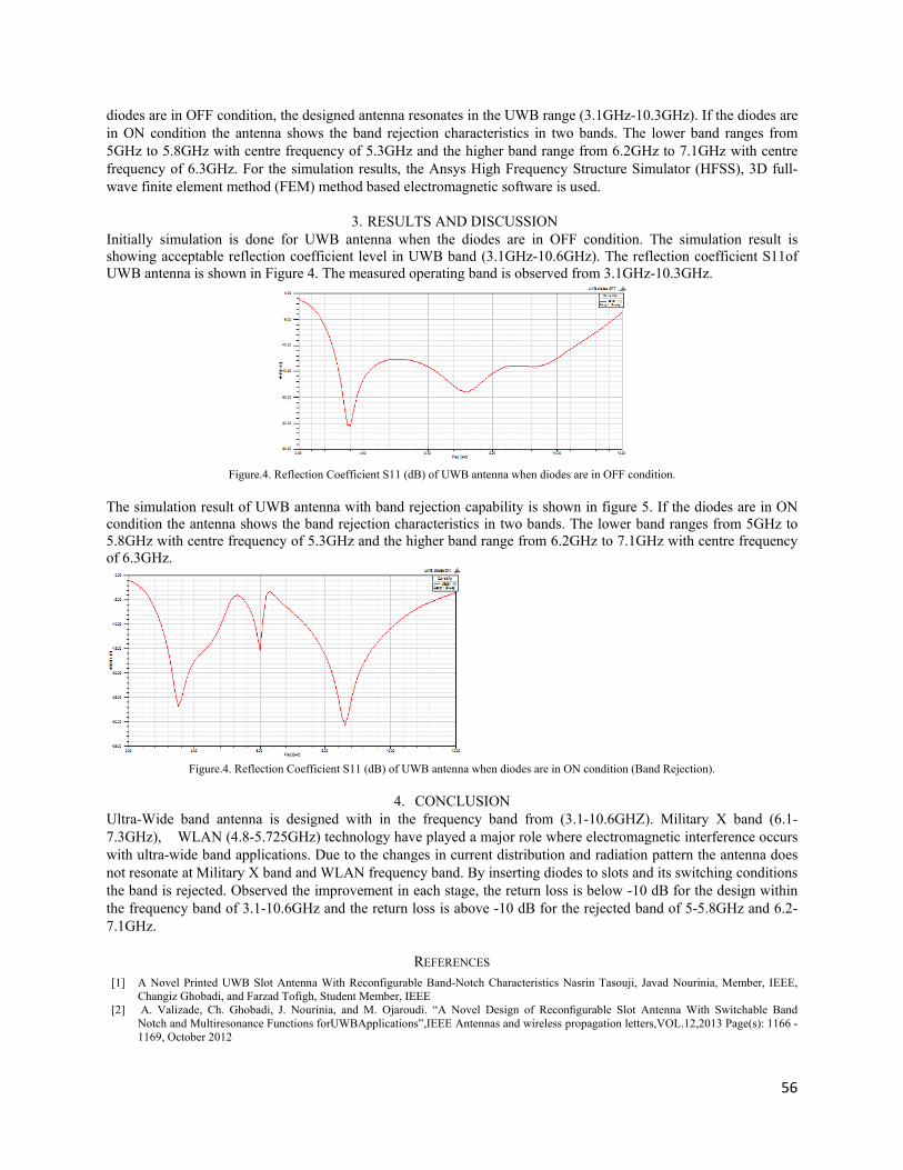
diodes are in OFF condition, the designed antenna resonates in the UWB range (3.1GHz-10.3GHz). If the diodes are in ON condition the antenna shows the band rejection characteristics in two bands. The lower band ranges from 5GHz to 5.8GHz with centre frequency of 5.3GHz and the higher band range from 6.2GHz to 7.1GHz with centre frequency of 6.3GHz. For the simulation results, the Ansys High Frequency Structure Simulator (HFSS), 3D full-wave finite element method (FEM) method based electromagnetic software is used.
3. RESULTS AND DISCUSSION Initially simulation is done for UWB antenna when the diodes are in OFF condition. The simulation result is showing acceptable reflection coefficient level in UWB band (3.1GHz-10.6GHz). The reflection coefficient S11of UWB antenna is shown in Figure 4. The measured operating band is observed from 3.1GHz-10.3GHz.
Figure.4. Reflection Coefficient S11 (dB) of UWB antenna when diodes are in OFF condition.
The simulation result of UWB antenna with band rejection capability is shown in figure 5. If the diodes are in ON condition the antenna shows the band rejection characteristics in two bands. The lower band ranges from 5GHz to 5.8GHz with centre frequency of 5.3GHz and the higher band range from 6.2GHz to 7.1GHz with centre frequency of 6.3GHz.
Figure.4. Reflection Coefficient S11 (dB) of UWB antenna when diodes are in ON condition (Band Rejection).
4. CONCLUSION Ultra-Wide band antenna is designed with in the frequency band from (3.1-10.6GHZ). Military X band (6.1-7.3GHz), WLAN (4.8-5.725GHz) technology have played a major role where electromagnetic interference occurs with ultra-wide band applications. Due to the changes in current distribution and radiation pattern the antenna does not resonate at Military X band and WLAN frequency band. By inserting diodes to slots and its switching conditions the band is rejected. Observed the improvement in each stage, the return loss is below -10 dB for the design within the frequency band of 3.1-10.6GHz and the return loss is above -10 dB for the rejected band of 5-5.8GHz and 6.2-7.1GHz.
REFERENCES [1] A Novel Printed UWB Slot Antenna With Reconfigurable Band-Notch Characteristics Nasrin Tasouji, Javad Nourinia, Member, IEEE,
Changiz Ghobadi, and Farzad Tofigh, Student Member, IEEE [2] A. Valizade, Ch. Ghobadi, J. Nourinia, and M. Ojaroudi. “A Novel Design of Reconfigurable Slot Antenna With Switchable Band
Notch and Multiresonance Functions forUWBApplications”,IEEE Antennas and wireless propagation letters,VOL.12,2013 Page(s): 1166 - 1169, October 2012

57
[3] Nasrin Tasouji, Javad Nourinia, Member, IEEE, Changiz Ghobadi, and Farzad Tofigh, “A Novel Printed UWB Slot Antenna With Reconfigurable Band-Notch Characteristics”. IEEE Antennas and wireless propagation letter IEEE. Page(s): 922 - 925, July 2013
[4] Bahareh Badamchi1, Javad Nourinia1, Changiz Ghobadi1, Arash Valizade Shahmirzadi “Design of compact reconfigurable ultra-wideband slot antenna with switchable single/dual band notch functions.” IET Microw. Antennas Propag. Page(s): 541 - 548.June 2014
[5] Chao-Ming Luo, Jing-Song Hong, Muhammad Amin, and Lei Zhong School of Physical Electronics,“Compact UWB Antenna with Triple Notched Bands Reconfigurable” .Electronics letters.June 2016
[6] Anudeepa S. Kholapure1 and R.G. Karandikar2. ,”Antenna with reconfigurable triple band notched characteristics for cognitive radio.” ICTACT Journal on communication technology ,2016
[7] K. V. Ajetrao A. P. Dhande, “Phi Shape UWB Antenna with Band Notch Characteristics.”, Engineering, Technology & Applied Science Research Vol. 8, No. 4, 2018
[8] Saeed Ur Rahman | Qunsheng Cao | Yi Wang | Habib Ullah. , “Design of wideband antenna with band notch characteristics based on single notching element” , Int Journal RF Microwave Computer Aided Eng, October 2018.
S