may/june 2018 - microchip technology
TRANSCRIPT

A MICROCHIP TECHNOLOGY INC. PUBLICATION
6 12 18Sense Your World
Reduce PCB Complexity and Cost
A Bias Towards DACs
MAY
/JUN
E 20
18
A MICROCHIP TECHNOLOGY INC. PUBLICATION
cont
ents
The Microchip name and logo, the Microchip logo, AnyRate, AVR, AVR logo, AVR Freaks, BeaconThings, BitCloud, CryptoMemory, CryptoRF, dsPIC, FlashFlex, flexPWR, Heldo, JukeBlox, KEELOQ, KEELOQ logo, Kleer, LANCheck, LINK MD, maXStylus, maXTouch, MediaLB, megaAVR, MOST, MOST logo, MPLAB, OptoLyzer, PIC, picoPower, PICSTART, PIC32 logo, Prochip Designer, QTouch, RightTouch, SAM-BA, SpyNIC, SST, SST Logo, SuperFlash, tinyAVR, UNI/O, and XMEGA are registered trademarks of Microchip Technology Incorporated in the U.S.A. and other countries. ClockWorks, The Embedded Control Solutions Company, EtherSynch, Hyper Speed Control, HyperLight Load, IntelliMOS, mTouch, Precision Edge, and Quiet-Wire are registered trademarks of Microchip Technology Incorporated in the U.S.A.Adjacent Key Suppression, AKS, Analog-for-the-Digital Age, Any Capacitor, AnyIn, AnyOut, BodyCom, chipKIT, chipKIT logo, CodeGuard, CryptoAuthentication, CryptoCompanion, CryptoController, dsPICDEM, dsPICDEM.net, Dynamic Average Matching, DAM, ECAN, EtherGREEN, In-Circuit Serial Programming, ICSP, Inter-Chip Connectivity, JitterBlocker, KleerNet, KleerNet logo, Mindi, MiWi, motorBench, MPASM, MPF, MPLAB Certified logo, MPLIB, MPLINK, MultiTRAK, NetDetach, Omniscient Code Generation, PICDEM, PICDEM.net, PICkit, PICtail, PureSilicon, QMatrix, RightTouch logo, REAL ICE, Ripple Blocker, SAM-ICE, Serial Quad I/O, SMART-I.S., SQI, SuperSwitcher, SuperSwitcher II, Total Endurance, TSHARC, USBCheck, VariSense, ViewSpan, WiperLock, Wireless DNA, and ZENA are trademarks of Microchip Technology Incorporated in the U.S.A. and other countries.SQTP is a service mark of Microchip Technology Incorporated in the U.S.A. Silicon Storage Technology is a registered trademark of Microchip Technology Inc. in other countries. GestIC and ULPP are registered trademarks of Microchip Technology Germany II GmbH & Co. & KG, a subsidiary of Microchip Technology Inc., in other countries. The LoRa name and associated logo are registered trademarks of Semtech Corporation or its subsidiaries. USB Type-C™ is a trademark of USB Implementers Forum. Arm and Cortex are registered trademarks of Arm Ltd. in the EU and other countries. All other trademarks mentioned herein are property of their respective companies. © 2018, Microchip Technology Incorporated, All Rights Reserved.
2
MAY
/JUN
E 20
18
COVER STORY 4 There’s a New Hero in Town
Your Favorite Tool for Debugging and Programming PIC® and dsPIC® Devices Is Now Even Better
NEW PRODUCTS 6 Sense Your World
New Family of 8-bit PIC Microcontrollers Is Ideal for Use in Sensor End Node Applications
8 Mission CriticalChoosing the Right Microcontroller to Create Responsive Command-and-Control Applications
10 Timing is EverythingNew Automotive-Grade MEMS Oscillators Meet Complex Demands of Emerging Automotive Applications
12 Reduce PCB Complexity and CostMicrochip’s First System on Module Features High-Performance SAMA5D27 Arm® Cortex®-A5 Based Microprocessor
NEW TOOL 14 Get Moving
Add Battery-Powered Activity Tracking, Security and Wireless Connectivity to Your New Medical Device Design
DESIGN CORNER 16 What Do You Need to Track?
18 A Bias Towards DACs
20 Why Google Cloud Platform?
23 Closing the IoT Security Loop
FEATURED VIDEO
Microchip MinutesSAM MCU Edition – Episode 1Low Power Overview
Microchip Technology Inc.2355 W. Chandler Blvd. | Chandler, AZ 85224 | www.microchip.com
Don’t Miss the Next Issue ofMicroSolutionsPublished six times a year, MicroSolutions is a valuable resource for product and technology news about Microchip’s innovative solutions. Subscribe today to receive email notifications when each new issue of MicroSolutions is ready. Use the link below:
Find Us on These Social Channels
CLICK TO SUBSCRIBE
EDITOR’S NOTE
3
A MICROCHIP TECHNOLOGY INC. PUBLICATION
6 12 18Sense Your World
Reduce PCB Complexity and Cost
A Bias Towards DACs
MAY
/JUN
E 20
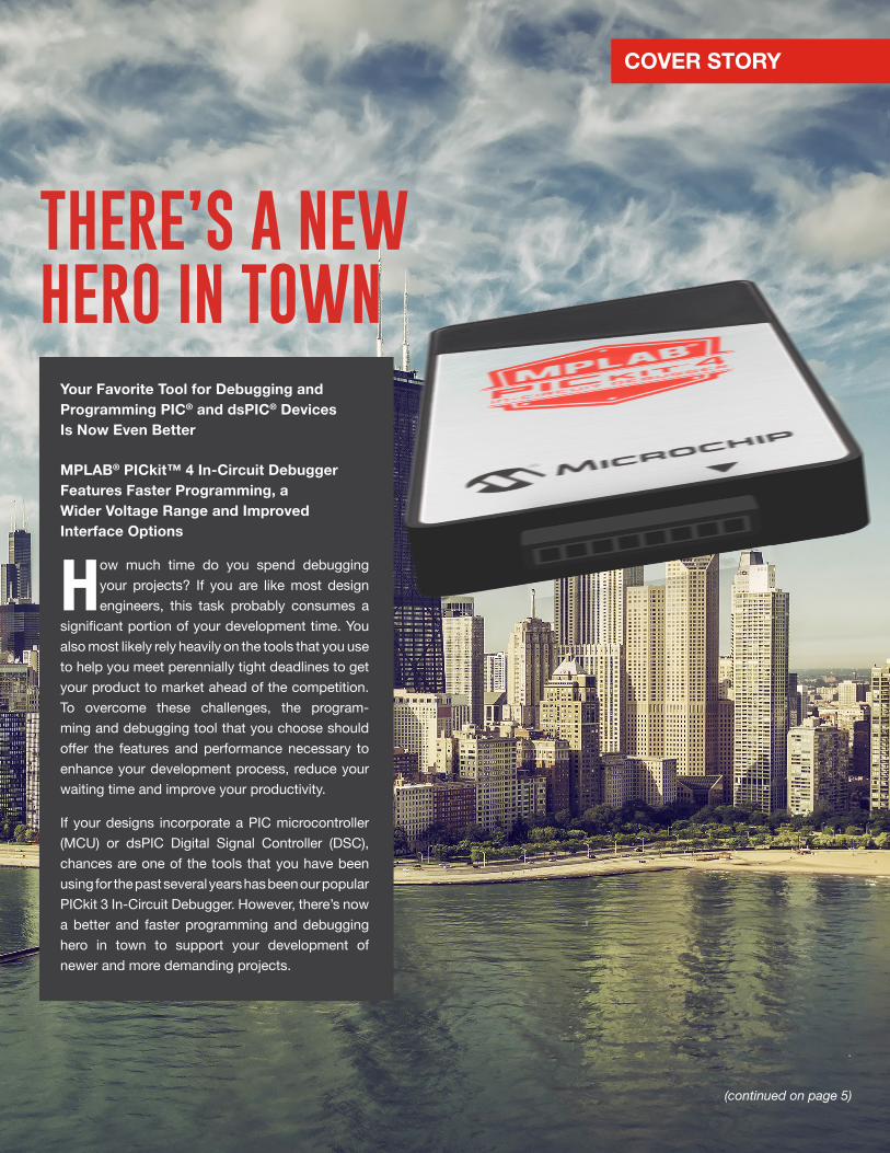
18An Incredible Journeywenty-seven years ago, few would have guessed that Microchip, a small semiconductor company just emerging from a pretty bleak situation, would grow to be recognized as a major industry leader and earn a place on the Nasdaq-100
Index. Steve Sanghi, currently Microchip’s Chief Executive Officer, has consistently led the company along its amazing trajectory to success that is marked by 109 consecutive quarters of profitability and a current sales revenue of approximately $4 billion.
On March 19, 2018, Microchip’s employees worldwide celebrated the 25th anniversary of Microchip’s Initial Public Offering (IPO) and listing on the Nasdaq Stock Market. To commemorate this significant milestone in the company’s history, Steve Sanghi had the honor of ringing the Closing Bell at the Nasdaq MarketSite in New York City on that same date. Noting that Microchip’s sales were only $89 million at the time of the IPO, Steve discussed the remarkable distance that the company has traveled. Over the ensuing years, Microchip has developed an extensive product portfolio through its strategy of new product development and strategic acquisitions. As a result, the company’s products are used in a vast array of applications being developed by over 115,000 customers worldwide.
We look forward to the future and continue to press towards our goal of being the very best embedded control solutions company ever. Our Microchip 2.0 growth initiative combines the company’s product, technology, system and employee strengths to enable us to offer Total System Solutions to our customers. This means that you can most likely find multiple Microchip solutions that will meet the requirements for your circuit board design.
We are here to provide you with the best devices, value and support to reduce your design risk and streamline your time to market. Visit www.microchip.com or get in touch with the nearest Microchip sales office to discuss your design goals and challenges with our technical sales and support professionals. We look forward to continuing our journey with you.
As always, we would be happy to get your feedback on MicroSolutions. Feel free to email us at [email protected].
3
EDITOR’S NOTE
T
Photo credit: Nasdaq, Inc.
4
(continued on page 5)
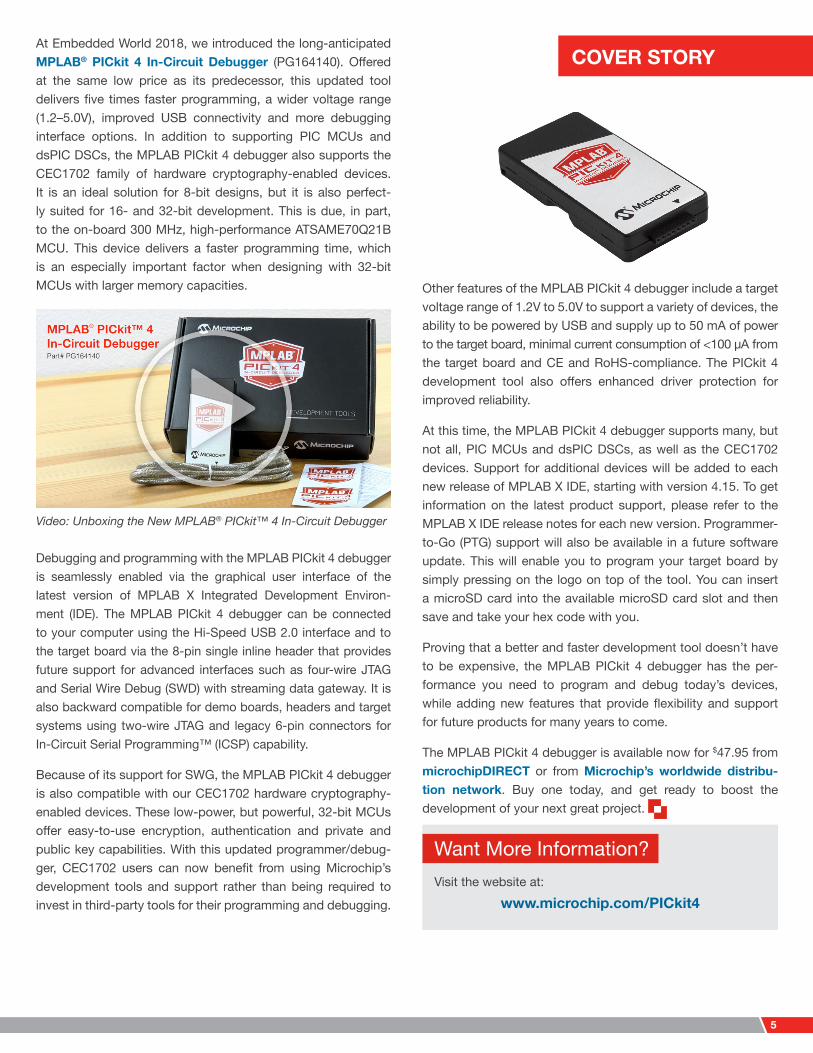
Your Favorite Tool for Debugging and Programming PIC® and dsPIC® Devices Is Now Even Better
MPLAB® PICkit™ 4 In-Circuit Debugger Features Faster Programming, a Wider Voltage Range and Improved Interface Options
How much time do you spend debugging your projects? If you are like most design engineers, this task probably consumes a
significant portion of your development time. You also most likely rely heavily on the tools that you use to help you meet perennially tight deadlines to get your product to market ahead of the competition. To overcome these challenges, the program-ming and debugging tool that you choose should offer the features and performance necessary to enhance your development process, reduce your waiting time and improve your productivity.
If your designs incorporate a PIC microcontroller (MCU) or dsPIC Digital Signal Controller (DSC), chances are one of the tools that you have been using for the past several years has been our popular PICkit 3 In-Circuit Debugger. However, there’s now a better and faster programming and debugging hero in town to support your development of newer and more demanding projects.
THERE’S A NEW HERO IN TOWN
COVER STORY
COVER STORY
5
At Embedded World 2018, we introduced the long-anticipated MPLAB® PICkit 4 In-Circuit Debugger (PG164140). Offered at the same low price as its predecessor, this updated tool delivers five times faster programming, a wider voltage range (1.2–5.0V), improved USB connectivity and more debugging interface options. In addition to supporting PIC MCUs and dsPIC DSCs, the MPLAB PICkit 4 debugger also supports the CEC1702 family of hardware cryptography-enabled devices. It is an ideal solution for 8-bit designs, but it is also perfect-ly suited for 16- and 32-bit development. This is due, in part, to the on-board 300 MHz, high-performance ATSAME70Q21B MCU. This device delivers a faster programming time, which is an especially important factor when designing with 32-bit MCUs with larger memory capacities.
Debugging and programming with the MPLAB PICkit 4 debugger is seamlessly enabled via the graphical user interface of the latest version of MPLAB X Integrated Development Environ-ment (IDE). The MPLAB PICkit 4 debugger can be connected to your computer using the Hi-Speed USB 2.0 interface and to the target board via the 8-pin single inline header that provides future support for advanced interfaces such as four-wire JTAG and Serial Wire Debug (SWD) with streaming data gateway. It is also backward compatible for demo boards, headers and target systems using two-wire JTAG and legacy 6-pin connectors for In-Circuit Serial Programming™ (ICSP) capability.
Because of its support for SWG, the MPLAB PICkit 4 debugger is also compatible with our CEC1702 hardware cryptography- enabled devices. These low-power, but powerful, 32-bit MCUs offer easy-to-use encryption, authentication and private and public key capabilities. With this updated programmer/debug-ger, CEC1702 users can now benefit from using Microchip’s development tools and support rather than being required to invest in third-party tools for their programming and debugging.
Video: Unboxing the New MPLAB® PICkit™ 4 In-Circuit Debugger
Other features of the MPLAB PICkit 4 debugger include a target voltage range of 1.2V to 5.0V to support a variety of devices, the ability to be powered by USB and supply up to 50 mA of power to the target board, minimal current consumption of <100 μA from the target board and CE and RoHS-compliance. The PICkit 4 development tool also offers enhanced driver protection for improved reliability.
At this time, the MPLAB PICkit 4 debugger supports many, but not all, PIC MCUs and dsPIC DSCs, as well as the CEC1702 devices. Support for additional devices will be added to each new release of MPLAB X IDE, starting with version 4.15. To get information on the latest product support, please refer to the MPLAB X IDE release notes for each new version. Programmer- to-Go (PTG) support will also be available in a future software update. This will enable you to program your target board by simply pressing on the logo on top of the tool. You can insert a microSD card into the available microSD card slot and then save and take your hex code with you.
Proving that a better and faster development tool doesn’t have to be expensive, the MPLAB PICkit 4 debugger has the per-formance you need to program and debug today’s devices, while adding new features that provide flexibility and support for future products for many years to come.
The MPLAB PICkit 4 debugger is available now for $47.95 from microchipDIRECT or from Microchip’s worldwide distribu-tion network. Buy one today, and get ready to boost the development of your next great project.
Want More Information?Visit the website at:
www.microchip.com/PICkit4
NEW PRODUCTS
6
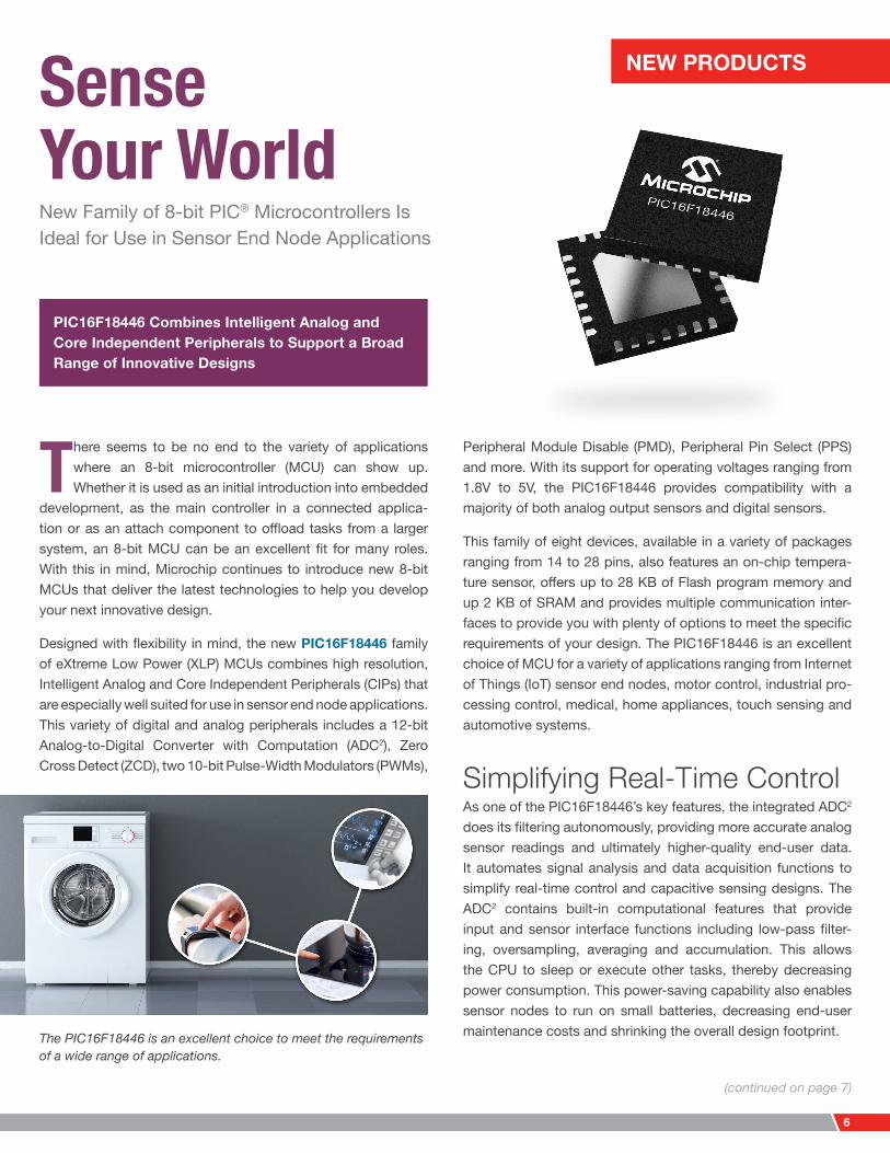
Sense Your WorldNew Family of 8-bit PIC® Microcontrollers Is Ideal for Use in Sensor End Node Applications
Peripheral Module Disable (PMD), Peripheral Pin Select (PPS) and more. With its support for operating voltages ranging from 1.8V to 5V, the PIC16F18446 provides compatibility with a majority of both analog output sensors and digital sensors.
This family of eight devices, available in a variety of packages ranging from 14 to 28 pins, also features an on-chip tempera-ture sensor, offers up to 28 KB of Flash program memory and up 2 KB of SRAM and provides multiple communication inter-faces to provide you with plenty of options to meet the specific requirements of your design. The PIC16F18446 is an excellent choice of MCU for a variety of applications ranging from Internet of Things (IoT) sensor end nodes, motor control, industrial pro-cessing control, medical, home appliances, touch sensing and automotive systems.
Simplifying Real-Time ControlAs one of the PIC16F18446’s key features, the integrated ADC2 does its filtering autonomously, providing more accurate analog sensor readings and ultimately higher-quality end-user data. It automates signal analysis and data acquisition functions to simplify real-time control and capacitive sensing designs. The ADC2 contains built-in computational features that provide input and sensor interface functions including low-pass filter-ing, oversampling, averaging and accumulation. This allows the CPU to sleep or execute other tasks, thereby decreasing power consumption. This power-saving capability also enables sensor nodes to run on small batteries, decreasing end-user maintenance costs and shrinking the overall design footprint.
There seems to be no end to the variety of applications where an 8-bit microcontroller (MCU) can show up. Whether it is used as an initial introduction into embedded
development, as the main controller in a connected applica-tion or as an attach component to offload tasks from a larger system, an 8-bit MCU can be an excellent fit for many roles. With this in mind, Microchip continues to introduce new 8-bit MCUs that deliver the latest technologies to help you develop your next innovative design.
Designed with flexibility in mind, the new PIC16F18446 family of eXtreme Low Power (XLP) MCUs combines high resolution, Intelligent Analog and Core Independent Peripherals (CIPs) that are especially well suited for use in sensor end node applications. This variety of digital and analog peripherals includes a 12-bit Analog-to-Digital Converter with Computation (ADC2), Zero Cross Detect (ZCD), two 10-bit Pulse-Width Modulators (PWMs),
PIC16F18446 Combines Intelligent Analog and Core Independent Peripherals to Support a Broad Range of Innovative Designs
(continued on page 7)
The PIC16F18446 is an excellent choice to meet the requirements of a wide range of applications.
NEW PRODUCTS
7
Enhanced System FeaturesMemory Access Partition (MAP) is a customizable Flash memory area that supports bootloader write protection to prevent acci-dental over-write for data protection. Device Information Area (DIA) offers protected storage for unique device identification and contains calibration data for the internal temperature sensor module and the Fixed Voltage Reference (FVR) reading.
Low-Power CapabilitiesIf you are designing a battery-powered application, you need to be able to optimize device performance and power consump-tion to extend battery life. The PIC16F18446 offers sleep cur-rents are as low as 50 nA as well as power saving functions like IDLE and DOZE modes. IDLE mode puts the CPU core to sleep while the internal peripherals continue to operate from the system clock. DOZE mode enables the CPU core to run at a slower speed than the system clock that is used by the internal peripherals. The Peripheral Module Disable (PMD) allows unused peripherals to be turned off individually, further reducing power consumption.
Faster Time to MarketInherently simple to understand and implement, the PIC16F18446 family’s Core Independent Peripherals enable you to accomplish tasks in hardware while freeing up the CPU to do other tasks or go to sleep. These hardware-based periph-erals offload timing-critical and core-intensive functions from the CPU, allowing it to focus on other critical tasks within the
Video: Overview of PIC16F18446 Family of 8-bit Microcontrollers
system. This decreases system complexity by eliminating the need for additional code and external components and also reduces power consumption, which allows for deterministic response time and decreased validation time.
Development ToolsTo further reduce your time to market, you can take advantage our comprehensive, easy-to-use development ecosystem. The PIC16F18446 family of MCUs is supported by MPLAB® Code Configurator (MCC). This free plug-in for use with MPLAB X Integrated Development Environment (IDE) or the cloud-based MPLAB Xpress IDE provides a graphical programming environment that generates seamless, easy-to-understand C code to be inserted into your project. Using an intuitive inter-face, it enables and configures a rich set of peripherals and functions specific to your application.
Available for a limited time and while supplies last, the MPLAB Xpress PIC16F18446 Evaluation Board will help jumpstart the development of your projects. It features the 20-pin PIC16F18446 MCU as the on-board processor and a unique drag-and-drop programmer for compatibility with almost any USB-connected PC, laptop or tablet without requiring any drivers. It also has a mikroBUS™-compatible socket, allowing for the easy addition of sensors, actuators or communications interfaces from Mikro-Elektronika’s extensive library of click boards™. The MPLAB Xpress PIC16F18446 Evaluation Board integrates seamlessly with our software tool chain so that you can quickly and easily build a working prototype in a short period of time.
If you are ready to begin creating a design to sense your world, the PIC16F18446 is available in a variety of packages and can be purchased from microchipDIRECT or from Microchip’s worldwide distribution network.
Want More Information?Visit the website at:
www.microchip.com/PIC16F18446Family
NEW PRODUCTS
8
Mission CriticalChoosing the Right Microcontroller to Create Responsive Command-and-Control Applications
hardware instead of through software. This decreases the amount of code needed and can tremendously reduce software efforts for faster time to market. For example, the Configurable Custom Logic (CCL) peripheral can connect the ADC to a cus-tomized combination of external triggers through hardware without interrupting the core, which improves response time while reducing power consumption. The ATmega4809 can also be added to a system to offload functions from more complex microprocessor (MPU) based designs. By using CIPs to execute command and control tasks in the MCU instead of in the MPU, the risk of delayed responses is decreased, resulting in a better end-user experience.
The Peripheral Event System is another important building
block for implementing real-time control.
The Peripheral Event System is another important building block for implementing real-time control in your application. This hardware-based connectivity matrix allows the peripherals on the ATmega4809 to communicate with one another without involving the core CPU. You can use this functionality to save energy, increase determinism in control loops, or both. Most importantly, the Event System is easily configured with our free software tools, helping decrease system validation time.
Microcontrollers (MCUs) are used in modern real-time control applications to increase their performance while also making them more efficient and reliable. For
many of these types of systems, analog data acquisition and processing are mission critical. The right MCU will decrease system response time and increase reliability while also helping to meet critical design requirements to reduce overall code footprint, validation time and development costs.
A new series of 8-bit megaAVR MCUs is now available to help you create highly responsive command-and-control applica-tions. The ATmega4809 family combines intelligent hardware peripherals with the low-power performance of the AVR® MCU core to extend the capabilities of real-time control systems. The processing power of the integrated high-speed Analog-to- Digital Converter (ADC) enables faster conversion of analog signals, resulting in deterministic system responses.
As the first megaAVR device to include Core Independent Peripherals (CIPs), the ATmega4809 can execute tasks in
New Series of 8-bit megaAVR® Devices Is Engineered for Real-Time Control
(continued on page 9)
Create highly responsive command-and-control applications with the ATmega4809.
NEW PRODUCTS
9
This new family of megaAVR MCUs uses the same robust architecture as the latest tinyAVR® 0- and 1-series devices, while offering increased memory and I/O options. With up to 48 KB of Flash memory in 28-, 32- and 48-pin packages, these devices suit a wide variety of application needs. They are ideal companions in complex MPU-based systems, or excellent standalone processors for use in command-and-control system designs.
The ATmega4809 has also been selected to be the on-board microcontroller of a next-generation Arduino® board. The addi-tion of the ATmega4809 to this board will allow developers to spend less time coding and more time creating. The hardware- based CIPs enable the creation of designs which are more efficient, while making the transition from project to production-ready easier than ever before.
Video: Overview of the ATmega4809 High-Performance AVR® Microcontroller
Development ToolsTo help jumpstart your development, the ATmega4809 Xplained Pro Evaluation Kit (ATmega4809-XPRO) is a USB-powered kit for rapid prototyping with the ATmega4809. It features touch buttons, LEDs and extension headers for quick setup, as well as an on-board programmer/debugger that seamlessly integrates with Atmel Studio 7 Integrated Development Environment (IDE) and Atmel START, a free online tool to configure peripher-als and software that accelerates development. This board also has a mikroBUS™-compatible socket, allowing for the easy addition of sensors, actuators or communications interfaces from MikroElektronika’s extensive library of click boards™.
To add the ATmega4809 to your latest command-and-control application, you can order it from microchipDIRECT or from Microchip’s worldwide distribution network.
Want More Information?Visit the website at:
www.microchip.com/ATmega4809
NEW PRODUCTS
10
Timing is EverythingNew Automotive-Grade MEMS Oscillators Meet Complex Demands of Emerging Automotive Applications
times and fixed frequency. Product development or release times can be delayed if a last-minute frequency change needs to be made. MEMS oscillators achieve frequency through pro-gramming, giving them the flexibility to quickly support new fre-quencies with shorter lead times. Because of this, they can also be rapidly ramped up to volume production to help meet tight product launch schedules.
MEMS oscillators achieve frequency
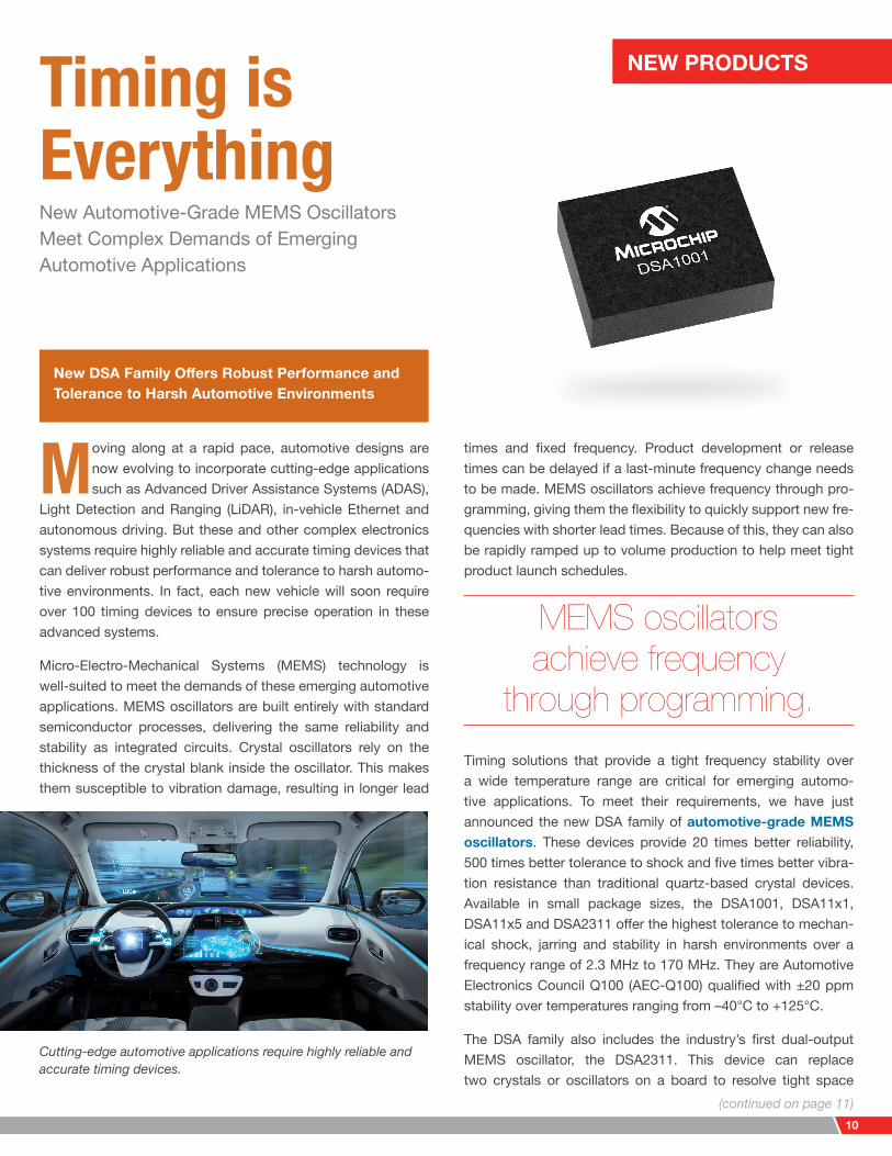
through programming.Timing solutions that provide a tight frequency stability over a wide temperature range are critical for emerging automo-tive applications. To meet their requirements, we have just announced the new DSA family of automotive-grade MEMS oscillators. These devices provide 20 times better reliability, 500 times better tolerance to shock and five times better vibra-tion resistance than traditional quartz-based crystal devices. Available in small package sizes, the DSA1001, DSA11x1, DSA11x5 and DSA2311 offer the highest tolerance to mechan-ical shock, jarring and stability in harsh environments over a frequency range of 2.3 MHz to 170 MHz. They are Automotive Electronics Council Q100 (AEC-Q100) qualified with ±20 ppm stability over temperatures ranging from –40°C to +125°C.
The DSA family also includes the industry’s first dual-output MEMS oscillator, the DSA2311. This device can replace two crystals or oscillators on a board to resolve tight space
Moving along at a rapid pace, automotive designs are now evolving to incorporate cutting-edge applications such as Advanced Driver Assistance Systems (ADAS),
Light Detection and Ranging (LiDAR), in-vehicle Ethernet and autonomous driving. But these and other complex electronics systems require highly reliable and accurate timing devices that can deliver robust performance and tolerance to harsh automo-tive environments. In fact, each new vehicle will soon require over 100 timing devices to ensure precise operation in these advanced systems.
Micro-Electro-Mechanical Systems (MEMS) technology is well-suited to meet the demands of these emerging automotive applications. MEMS oscillators are built entirely with standard semiconductor processes, delivering the same reliability and stability as integrated circuits. Crystal oscillators rely on the thickness of the crystal blank inside the oscillator. This makes them susceptible to vibration damage, resulting in longer lead
New DSA Family Offers Robust Performance and Tolerance to Harsh Automotive Environments
(continued on page 11)
Cutting-edge automotive applications require highly reliable and accurate timing devices.

NEW PRODUCTS
11
constraints, save costs and ease the design process. The DSA2311 comes in a concise 2.5 mm × 2.0 mm package and is well suited for applications that require a complex board with multiple controllers, such as infotainment systems and camera modules.
Development SupportOur ClockWorks® Configurator, a free online tool, makes it easy to select the right automotive-grade MEMS oscillator based on the frequency, package size and temperature range
that your design requires, and it also enables you to order free samples to get started with prototyping your project.
Devices in the DSA family of MEMS oscillators are some of the latest additions to Microchip’s comprehensive portfolio of automotive solutions, including microcontrollers, analog prod-ucts and connectivity components. This gives you the ability to consolidate suppliers for your system needs, plus get the extra assurance of knowing that these products are backed by Microchip’s customer-driven obsolescence policy, which ensures that devices will be available for as long as you need them.
If you are looking for timing devices that offer better performance, reliability and longevity for your automotive design, you can pur-chase devices in the DSA family from microchipDIRECT or from Microchip’s worldwide distribution network.
Want More Information?Visit the website at:
www.microchip.com/timing/automotive
ADASFrequency stability, robustness
InfotainmentSmall size, EMI reduction
ClusterSmall size, multi-options
Engine Control UnitTemperature performance,robustness
Adaptive HeadlightsEMI reduction, small size
Diagnosis UnitTemperature performance,small size
Anti-Lock Braking SystemRobustness, temperature performance
Transmission ControlRobustness, temperature performance
EthernetStability, low-jitter
Surround CamerasSmall size, robustness
Figure 1: Applications for Timing Solutions in Modern Vehicles
Click to Learn More
2018
MicrochipMASTERs The Premier Technical Training Conference
for Embedded Control Engineers
Phoenix, ArizonaWeek of August 20
(3½ or 5½ Day Programs)
Mark Your Calendars!
NEW PRODUCTS
12
Reduce PCB Complexity and CostMicrochip’s First System on Module Features High-Performance SAMA5D27 Arm® Cortex®-A5 Based Microprocessor
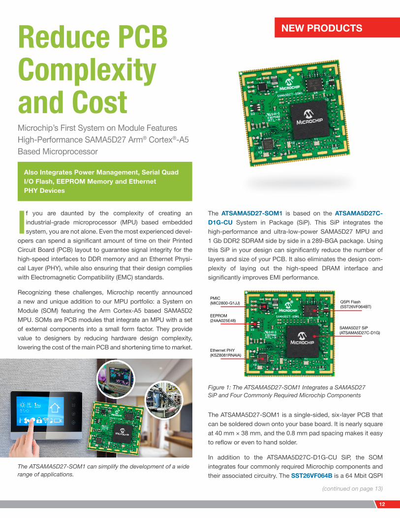
The ATSAMA5D27-SOM1 is based on the ATSAMA5D27C- D1G-CU System in Package (SiP). This SiP integrates the high-performance and ultra-low-power SAMA5D27 MPU and 1 Gb DDR2 SDRAM side by side in a 289-BGA package. Using this SiP in your design can significantly reduce the number of layers and size of your PCB. It also eliminates the design com-plexity of laying out the high-speed DRAM interface and significantly improves EMI performance.
The ATSAMA5D27-SOM1 is a single-sided, six-layer PCB that can be soldered down onto your base board. It is nearly square at 40 mm × 38 mm, and the 0.8 mm pad spacing makes it easy to reflow or even to hand solder.
In addition to the ATSAMA5D27C-D1G-CU SiP, the SOM integrates four commonly required Microchip components and their associated circuitry. The SST26VF064B is a 64 Mbit QSPI
PMIC(MIC2800-G1JJ)
EEPROM(24AA025E48)
Ethernet PHY(KSZ8081RNAIA)
QSPI Flash(SST26VF064BT)
SAMA5D27 SiP(ATSAMA5D27C-D1G)
If you are daunted by the complexity of creating an industrial-grade microprocessor (MPU) based embedded system, you are not alone. Even the most experienced devel-
opers can spend a significant amount of time on their Printed Circuit Board (PCB) layout to guarantee signal integrity for the high-speed interfaces to DDR memory and an Ethernet Physi-cal Layer (PHY), while also ensuring that their design complies with Electromagnetic Compatibility (EMC) standards.
Recognizing these challenges, Microchip recently announced a new and unique addition to our MPU portfolio: a System on Module (SOM) featuring the Arm Cortex-A5 based SAMA5D2 MPU. SOMs are PCB modules that integrate an MPU with a set of external components into a small form factor. They provide value to designers by reducing hardware design complexity, lowering the cost of the main PCB and shortening time to market.
Also Integrates Power Management, Serial Quad I/O Flash, EEPROM Memory and Ethernet PHY Devices
(continued on page 13)
The ATSAMA5D27-SOM1 can simplify the development of a wide range of applications.
Figure 1: The ATSAMA5D27-SOM1 Integrates a SAMA5D27 SiP and Four Commonly Required Microchip Components
NEW PRODUCTS
13
NOR Flash memory device that can be used to store the Linux® kernel or a Real-Time Operating System (RTOS) and/or user application code. The MIC2800 Power Management IC (PMIC) provides three regulated voltage outputs: 1.2 volts for the CPU, 1.7 volts for the DRAM in the SiP and 3.3 volts for everything else. The KSZ8081 10/100 Ethernet PHY transceiver and the 24AA025E48 serial EEPROM with a Media Access Control (MAC) address combine to add an Ethernet communication interface for the user console. Access to the peripheral features of the SAMA5D27 MPU is provided by 103 I/O lines. The ATSAMA5D27-SOM1 is certified for the industrial temperature range (–40°C to +85°C) and is designed to accommodate an optional metallic shield to reduce its exposure to external electro-magnetic radiation.
Lorem
Pin 1 of Module
25 MHz Crystal
PMIC
EEPROM
32 kHz Crystal
24 MHz Crystal
QSPI FLASH
Ethernet PHY
(SST26VF064B)(MIC2800-G1JJ)
(24AA025E48)
SAMA5D27 SiP(SAMA5D27C-D1G)
(KSZ8081RNAIA)
The ATSAMA5D27-SOM1’s design and components provide an optimized reference implementation for any system based on a SAMA5D2 SiP. To make it easy to get started with your layout, all the schematics and Gerber files you need are available free of charge. Based on our customer-driven obsolescence prac-tice, you can design the SOM into your application with confi-dence knowing that this solution will be available until you decide you no longer need it.
0.8 mm
PIN 1 CORNER40 mm
38 m
m 0.8 mm
0.2 mm
0.6 mm0.4 mm
The SAMA5D27 SOM1 Evaluation Kit 1 (ATSAMA5D27-SOM1-EK1) is a convenient evaluation and application development platform offering additional design support for your project. This board provides many connectivity interfaces including USB, Eth-ernet, standard SD card and microSD card, 24-bit parallel TFT LCD, JTAG, CAN and two mikroBUS™ click expansion headers to support over 300 MikroElektronika click boards™. Switches and a multi-color LED support user inputs and feedback.
Support for software development is available on the Linux4SAM wiki site, including board demo images and support for AT91 Bootstrap, U-Boot, Buildroot and Yocto build systems. We support the SAMA5D2 family in the mainline Linux OS distribu-tion. A SAMA5D2 software package (SoftPack) provides driver and demo code example support for RTOS and bare metal software development.
If you are ready to get started with your new design, you can purchase the ATSAMA5D27-SOM1 from microchipDIRECT or from Microchip’s worldwide distribution network. Visit our website to learn more about the SAMA5D2 SiP and SOM.
Want More Information?Visit the website at:
www.microchip.com/SAMA5D2SOM
Figure 2: ATSAMA5D27-SOM1 Dimensions
Figure 3: ATSAMA5D27-SOM1 Device Placement
SAMA5D27 SOM1 Evaluation Kit 1
NEW TOOL
14
Get MovingAdd Battery-Powered Activity Tracking, Security and Wireless Connectivity to Your New Medical Device Design
sleep quality, heart rate, body temperature, blood oxygen and other health-related parameters. Bluetooth® Low Energy (BLE) connectivity allows the demonstration board to wirelessly com-municate with tablets, smartphones or PCs so you can develop a smart health solution for the Internet of Things (IoT).*
Develop a smart health solution for the
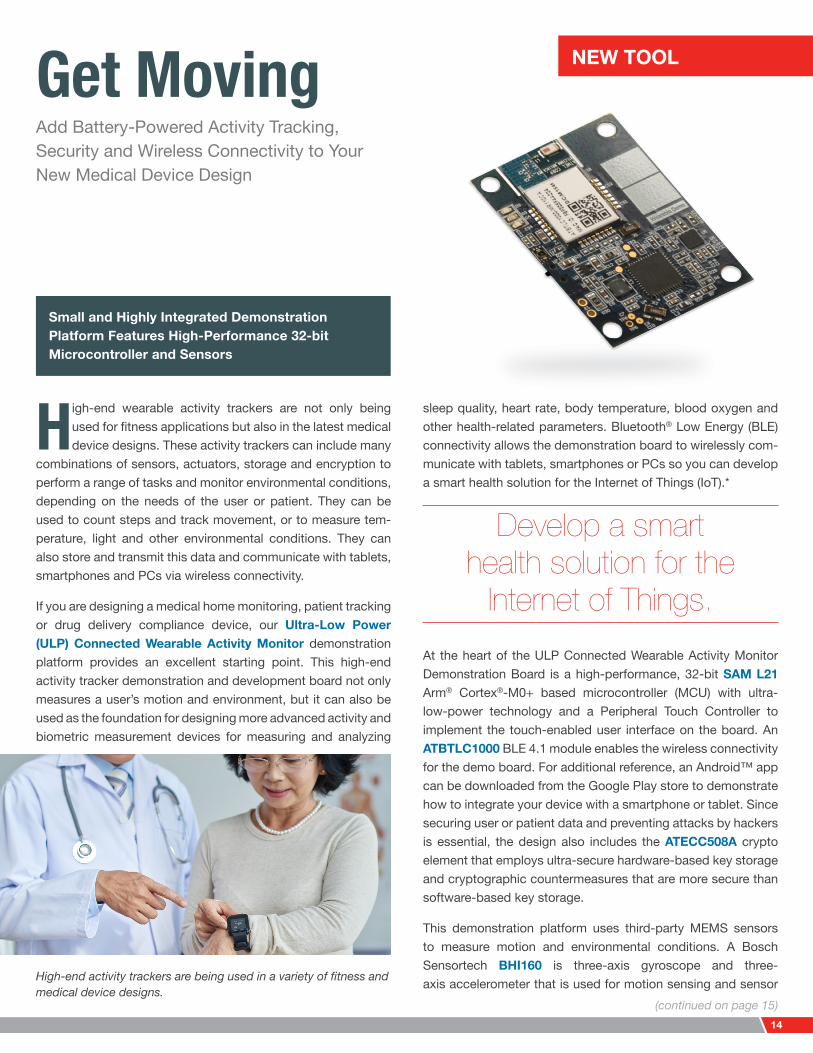
Internet of Things.At the heart of the ULP Connected Wearable Activity Monitor Demonstration Board is a high-performance, 32-bit SAM L21 Arm® Cortex®-M0+ based microcontroller (MCU) with ultra-low-power technology and a Peripheral Touch Controller to implement the touch-enabled user interface on the board. An ATBTLC1000 BLE 4.1 module enables the wireless connectivity for the demo board. For additional reference, an Android™ app can be downloaded from the Google Play store to demonstrate how to integrate your device with a smartphone or tablet. Since securing user or patient data and preventing attacks by hackers is essential, the design also includes the ATECC508A crypto element that employs ultra-secure hardware-based key storage and cryptographic countermeasures that are more secure than software-based key storage.
This demonstration platform uses third-party MEMS sensors to measure motion and environmental conditions. A Bosch Sensortech BHI160 is three-axis gyroscope and three- axis accelerometer that is used for motion sensing and sensor
High-end wearable activity trackers are not only being used for fitness applications but also in the latest medical device designs. These activity trackers can include many
combinations of sensors, actuators, storage and encryption to perform a range of tasks and monitor environmental conditions, depending on the needs of the user or patient. They can be used to count steps and track movement, or to measure tem-perature, light and other environmental conditions. They can also store and transmit this data and communicate with tablets, smartphones and PCs via wireless connectivity.
If you are designing a medical home monitoring, patient tracking or drug delivery compliance device, our Ultra-Low Power (ULP) Connected Wearable Activity Monitor demonstration platform provides an excellent starting point. This high-end activity tracker demonstration and development board not only measures a user’s motion and environment, but it can also be used as the foundation for designing more advanced activity and biometric measurement devices for measuring and analyzing
Small and Highly Integrated Demonstration Platform Features High-Performance 32-bit Microcontroller and Sensors
(continued on page 15)
High-end activity trackers are being used in a variety of fitness and medical device designs.
NEW TOOL
15
data processing. Also from Bosch Sensortec, a BME280 environmental sensor is used to measure humidity, pressure and temperature. The design also includes Vishay’s VEML6030 high-accuracy ambient light sensor. The sensor network is connected to the SAM L21 MCU through a two-wire interface.
Powered from a single 3V lithium coin cell battery, this small and low-power demonstration platform is an excellent option for developing medical patient tracking, patient compliance, patient biometric diagnostics, fitness activity tracking and other designs. The integrated sensors can be used to measure proximity, step count, free fall (detection), gyroscopic motion, ambient temperature, pressure (altitude), humidity and light. It also makes it easy to develop more advanced activity tracker functions (e.g. distance travelled, calories burned, sleep anal-ysis). Other biometric measurement capability—such as heart rate, blood oxygen and body temperature—can be added using our other medical reference designs. This platform’s high
level of integration results in low overall BOM cost to help you develop a competitively priced end product.
To help you get started with your wearable activity monitor design, you can download the user guide, schematics, hard-ware design package, firmware and demo app code for free from the ULP Connected Wearable Activity Monitor page on our website. If you would like to see a working demonstration of this reference design or have any questions about it, please contact your local Microchip Sales Representative.
*Microchip medical reference designs and demos are intended for evaluation and development purposes only. Use of Microchip devices in life support and/or safety applications is entirely at the buyer’s risk, and the buyer agrees to defend, indemnify and hold harmless Microchip from any and all damages, claims, suits, or expenses resulting from such use.
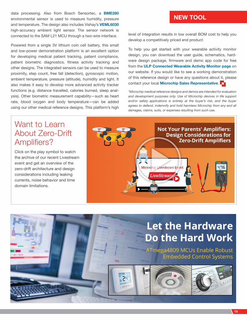
Want to Learn About Zero-Drift Amplifiers?Click on the play symbol to watch the archive of our recent Livestream event and get an overview of the zero-drift architecture and design considerations including leaking currents, noise behavior and time domain limitations.

DESIGN CORNER
16
For developers of many applications, the ability to identify and track detachable items—like connection wires, plastic tubes and printer cartridges—has long been considered
a nice-to-have feature. However, the difficulty of figuring out a low-cost way to add this capability to the manufacturing process usually results in this idea being left behind on the white board.
But we have an answer to this design challenge. The AT21CS01 is one of our highly reliable Single-Wire 1 Kb Serial EEPROMs that comes with a unique factory-programmed 64-bit serial number. It also offers a separate 128-bit user-writable space and four 256-bit EEPROM zones. The user can choose to make all five EEPROM zones (128-bit writable space and four 256-bit blocks) permanently written at any time so they can’t be hacked or accidentally changed.
The AT21CS01 uses a modified I2C interface that allows the device to extract power (Vcc) from the reading and writing sequences (pin SI/O). The second connection is system ground (pin Vss).
With this solution in mind, here are two examples of how the AT21CS01 1 Kb Serial EEPROM can be effectively used to provide a relatively low-cost solution for identifying and tracking detachable components.
(continued on page 17)
What Do You Need to Track?
Single-Wire Serial EEPROMs Provide Unique Serial Numbers to Help Identify and Track Detachable Components
Challenge #1 Medical Plastic TubingDesign Goals: A medical device uses a plastic tube that needs to be tracked. A new plastic tube must be assigned to and stay with each patient who uses the device. The base machine also may need to be shared with other patients. The device needs to reconfirm the tube identity on each insertion and read the tube usage history. The tube’s memory needs to track items such as patient ID number, timestamps for when it was used and possibly other data.
Figure 1: Using an AT21C201 Single-Wire EEPROM in a Medical Tubing Application
DESIGN CORNER
17
Concerns: The design uses low-temperature plastics that can’t endure high temperature cycles. Contact reliability is import-ant. Also, solder paste chemicals should not be used near the inhalation plastics.
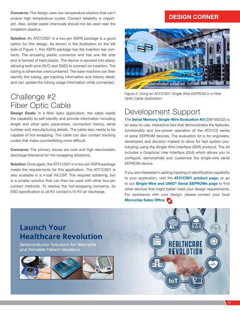
Solution: An AT21CS01 in a two-pin XSFN package is a good option for this design. As shown in the illustration on the left side of Figure 1, this XSFN package has flat insertion bar con-tacts. The encasing plastic connector end has one flat side and is formed of hard plastic. The device is epoxied into place, allowing both pins (SI/O and GND) to connect on insertion. The tubing is otherwise unencumbered. The base machine can then identify the tubing, get tracking information and history detail, and can update the tubing usage information while connected.
Challenge #2 Fiber Optic CableDesign Goals: In a fiber optic application, the cable needs the capability to self-identify and provide information including length and other optic parameters, connection history, serial number and manufacturing details. The cable also needs to be capable of hot-swapping. The cable can also contain tracking codes that make counterfeiting more difficult.
Concerns: The primary issues are cost and high electrostatic discharge tolerance for hot-swapping situations.
Solution: Once again, the AT21CS01 in a two-pin XSFN package meets the requirements for this application. The AT21CS01 is also available in a 4-ball WLCSP. This requires soldering, but is a smaller solution that can then be used with other two-pin contact methods. To resolve the hot-swapping concerns, its ESD specification is ±8 KV contact/±15 KV air discharge.
Figure 2: Using an AT21CS01 Single-Wire EEPROM in a Fiber Optic Cable Application
Development SupportThe Serial Memory Single-Wire Evaluation Kit (DM160232) is an easy-to-use, interactive tool that demonstrates the features, functionality and low-power operation of the AT21CS series of serial EEPROM devices. The evaluation kit is for engineers, developers and decision makers to allow for fast system pro-totyping using the Single-Wire Interface (SWI) protocol. The kit includes a Graphical User Interface (GUI) which allows you to configure, demonstrate and customize the single-wire serial EEPROM device.
If you are interested in adding tracking or identification capability to your application, visit the AT21CS01 product page, or go to our Single-Wire and UNIO® Serial EEPROMs page to find other devices that might better meet your design requirements. For assistance with your design, please contact your local Microchip Sales Office.
18(continued on page 19)
A Bias Towards DACs
DESIGN CORNER
Using a Digital-to-Analog Converter to Enhance Radio Frequency Applications
Biasing voltages are used to optimize performance in a variety of tuning circuits in Radio Frequency (RF) applications. As shown in the following examples, a
Digital-to-Analog Converter (DAC) can be a valuable addition to these types of designs.
Some RF power amplifier applications—such as GSM and CDMA cellular base stations, radar, CATV and portable radio devices—use LDMOS transistors. However, due to the charge build-up in the Drain-Gate region, there can be significant drifts of quiescent current (Idq) at a fixed-gate bias voltage (Vgs) over temperature. The Idq changes proportionally with both the gate bias voltage and temperature. To maintain the maximum output power with high linearity, the Idq needs to be constant over time across all operating temperature ranges. To achieve this goal, the gate bias voltage needs to be adjusted during operation to compensate the temperature changes.
In these types of applications, a DAC like the MCP4716 or MCP4726 can be used in the bias control circuits to maintain the Idq within a ±4% range. You can read more about this type of solution in AN1326: Using the MCP4728 12-bit DAC for LDMOS Amplifier Bias Control Applications.
Some simple RF circuits use a varactor, or varicap, diode to provide a capacitance that can be varied by changing the applied voltage. These types of diodes are often used for tuning circuits, such as RF oscillators and filters found in wireless applications such as wireless microphones and radios.
The varactor diode is operated under reverse bias, which creates a depletion zone around the P-N junction. Changing the level of the reverse bias changes the thickness of the deple-tion region and, thus, the effective capacitance of the diode. Increasing voltage causes a decrease in capacitance. Varactor diodes are specified with a nominal capacitance value and the range of capacitance that can be achieved with a maximum and minimum voltage level. A DAC can provide a convenient, cost-effective solution for creating the variable bias voltage.
Using a DAC does introduce sources of potential error. The varactor is affected by any form of amplitude variation of the bias voltage, resulting in an undesired shift in capacitance. Deterministic errors can be accounted for when using the microcontroller to program the DAC output voltage.
DESIGN CORNER
19
The primary sources of error that should be considered include:
• Varactor nonlinearity • Offset errors • DAC Integral Nonlinearity (INL)
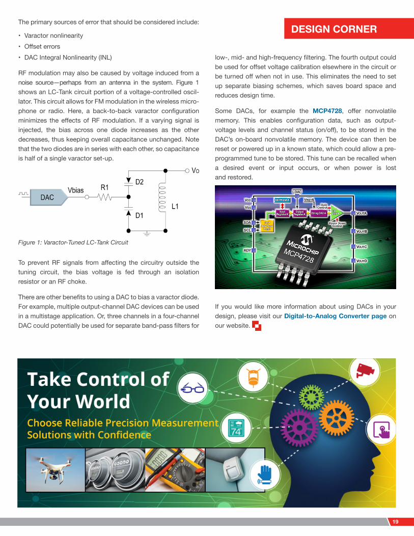
RF modulation may also be caused by voltage induced from a noise source—perhaps from an antenna in the system. Figure 1 shows an LC-Tank circuit portion of a voltage-controlled oscil-lator. This circuit allows for FM modulation in the wireless micro-phone or radio. Here, a back-to-back varactor configuration minimizes the effects of RF modulation. If a varying signal is injected, the bias across one diode increases as the other decreases, thus keeping overall capacitance unchanged. Note that the two diodes are in series with each other, so capacitance is half of a single varactor set-up.
To prevent RF signals from affecting the circuitry outside the tuning circuit, the bias voltage is fed through an isolation resistor or an RF choke.
There are other benefits to using a DAC to bias a varactor diode. For example, multiple output-channel DAC devices can be used in a multistage application. Or, three channels in a four-channel DAC could potentially be used for separate band-pass filters for
low-, mid- and high-frequency filtering. The fourth output could be used for offset voltage calibration elsewhere in the circuit or be turned off when not in use. This eliminates the need to set up separate biasing schemes, which saves board space and reduces design time.
Some DACs, for example the MCP4728, offer nonvolatile memory. This enables configuration data, such as output- voltage levels and channel status (on/off), to be stored in the DAC’s on-board nonvolatile memory. The device can then be reset or powered up in a known state, which could allow a pre- programmed tune to be stored. This tune can be recalled when a desired event or input occurs, or when power is lost and restored.
If you would like more information about using DACs in your design, please visit our Digital-to-Analog Converter page on our website.
Figure 1: Varactor-Tuned LC-Tank Circuit

DESIGN CORNER
20
Why Google Cloud Platform?
DESIGN CORNER
The Future of Computing is Flexibility: A Different Kind of CloudContributed by Google Cloud
Over the past two decades, we’ve seen three waves of innovation in the cloud computing market. The first wave was collocated hosting, giving customers financial effi-
ciencies in renting physical space rather than investing in data center real estate. The second wave, and what most clouds look like today, is the virtualized data center model where developers are still forced to spend much of their time “keeping the lights on” versus building great applications, and the third wave is a full-managed, serverless cloud environment.
About ten years ago, Google got sick of the limitations of physical, virtualized data centers and switched to a container- based, serverless architecture. This means developers don’t need to spin up servers, configure networks or patch operat-ing systems. They can focus on building innovative software, at scale. Products like YouTube, Gmail and Maps serve millions of users each minute. Yet the developers working on these appli-cations update production code multiple times a day without disruption, and their systems are resilient and secure.
Today, we’re delivering this vision to the rest of the world on Google Cloud Platform (GCP). With AppEngine, you never see servers or patches, and you can literally spend zero hours on administration per year. With BigQuery, you don’t have to provision and maintain an analytics cluster. With DataProc, our managed Hadoop and Spark service, you can be up and running in 90 seconds. We let customers focus on functionality, not managing infrastructure. Our customers are eager to leverage
services and technologies that have powered Google’s own internal infrastructure to build and deploy their solutions.
When building Google Cloud, we concentrated around three fundamental principles:
• Security, networking and infrastructure: Our infrastructure doesn’t rely on any single technology to make it secure. Rather, we build security through progressive layers that deliver true defense in depth. Our hardware infrastructure is also custom designed by Google “from chip to chiller” to precisely meet our requirements, including security. We operate one of the largest backbone networks in the world, connecting our data centers with hundreds of thousands of miles of fiber optic cable. According to a third-party estimate, more than 25% of global Internet traffic flows over our network in a given day. We have more than 100 points of presence across 33 coun-tries, and we continue adding and scaling zones and regions to meet customers’ preferences and policy requirements. The scale of our infrastructure allows us to absorb many Denial of Service (DoS) attacks, and we have multiple layers of pro-tection that further reduce the risk of any DoS impact. Finally, our operations teams detect threats and respond to incidents 24 × 7 × 365.
• Unlock data and accelerate development: Analytics and machine intelligence at web scale have been core to GCP
(continued on page 21)
DESIGN CORNER
21
since the beginning. Google BigQuery, Google Cloud Datalab and Google Cloud Dataproc—all based on the same distrib-uted data services that are used at Google—are changing how customers analyze and use data. Google is also known as a world leader in Artificial Intelligence (AI), with our ability to provide modern machine learning and pre-trained models for rich application development. We also have APIs for comput-er vision (video and still image), speech recognition (audio to text), natural language processing (gain context from words), translation and more. These services can be used by devel-opers with little to no experience using machine learning; they just need to be know how to use the API. This allows custom-ers to add machine learning technology to solve challenges in their business or provide new features to their customers.
• Open, enterprise-friendly: We think cloud customers need a flexible and responsive relationship with their providers. The best way to keep open source at the forefront is to build active communities around the technology. We are commit-ted to building communities around two of the most important innovations in the world: containers and machine learning. Kubernetes and Tensorflow are quickly becoming industry and developer standards, and we continue to invest in tech-nology that allows you to build the way you want. We believe, over time, you’ll value our investments in custom hardware, elastic compute and truly no ops services, but we aren’t going to hold you hostage with locked down/proprietary APIs. In fact, the latest release of Kubernetes is great for running federated clusters across zones, regions, or even across on-premises and cloud providers. Again, you choose the optimal architecture.
These three fundamental principles also make GCP an ideal cloud computing environment for the Internet of Things (IoT). Enterprises that rely on industrial devices such as sensors, conveyor belts, farming equipment, medical equipment and pumps—particularly, globally distributed ones—are struggling to monitor and manage these devices for several reasons, including operational cost and complexity, patchwork security, and data fragmentation. With Cloud IoT Core on GCP, custom-ers can easily connect and centrally manage millions of glob-ally dispersed connected devices. When used as part of the broader Google Cloud IoT solution, you can ingest all your IoT data and connect to our state-of-the-art analytics and machine learning services to gain actionable insights.
What about Security?In too many IoT implementations, Transport Layer Security (TLS) encryption is believed to provide sufficient security. But, just as you would not publish a list of social security numbers in a newspaper, you would not list private keys to all the web-sites using a network on a public web page. To provide the
best possible security, a device’s identity needs to be unique, protected, trusted and verifiable. A connected device’s private key is the most critical element in the authentication process. If a hacker owns your private key, he essentially becomes you.
For the past 20 years, the computing industry has been relying on trusted platform modules for security, while the phone industry has been using SIM cards to protect keys and cre-dentials. However, in today’s IoT devices, private keys often reside in the Flash memory of a microcontroller where they can be accessed very easily. Private keys can also be maliciously manipulated during the manufacturing of end products such as thermostats and HVAC systems, but also in more costly assets such as industrial equipment that is used to control major man-ufacturing plants. When the most critical source of security—the private key—is maliciously attacked, the identity of the IoT device is corrupted beyond the capabilities of any encryption scheme to protect it.
As security is one of the core principles of GCP, Microchip has partnered with the Cloud IoT Core to strengthen the authenti-cation security level between the IoT hardware and GCP. In a recent “Hardware Root of Trust with Google Cloud IoT Core and Microchip” webinar, representatives from Google Cloud Platform and Microchip discussed how to implement hardware- based security to meet the challenges of implementing an IoT solution. Our joint offering offers impressive benefits to the IoT developer including:
• Speeds up development time to reduce costs and accelerate time to market
• Easy-to-use solution reduces barriers and makes cloud technology accessible
• Global and proven robustness, elasticity and scalability; you pay for the way you use it, when you use it.
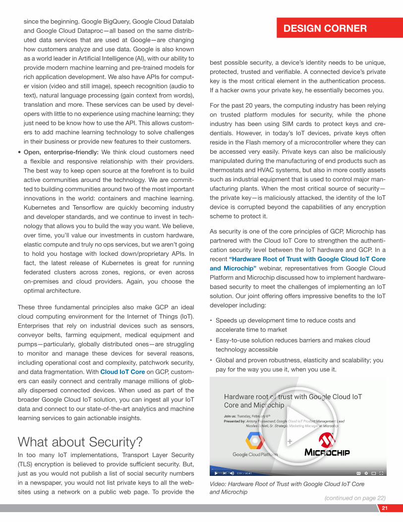
Video: Hardware Root of Trust with Google Cloud IoT Core and Microchip
(continued on page 22)
DESIGN CORNER
22
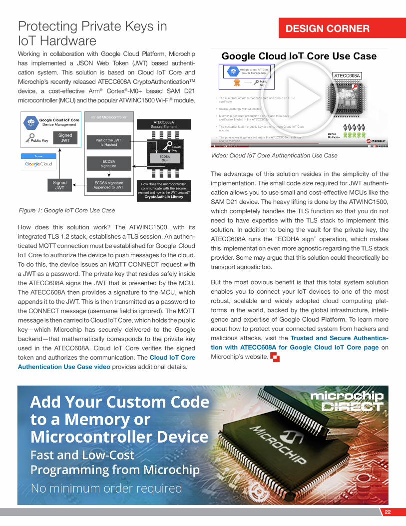
Protecting Private Keys in IoT HardwareWorking in collaboration with Google Cloud Platform, Microchip has implemented a JSON Web Token (JWT) based authenti-cation system. This solution is based on Cloud IoT Core and Microchip’s recently released ATECC608A CryptoAuthentication™ device, a cost-effective Arm® Cortex®-M0+ based SAM D21 microcontroller (MCU) and the popular ATWINC1500 Wi-Fi® module.
How does this solution work? The ATWINC1500, with its integrated TLS 1.2 stack, establishes a TLS session. An authen-ticated MQTT connection must be established for Google Cloud IoT Core to authorize the device to push messages to the cloud. To do this, the device issues an MQTT CONNECT request with a JWT as a password. The private key that resides safely inside the ATECC608A signs the JWT that is presented by the MCU. The ATECC608A then provides a signature to the MCU, which appends it to the JWT. This is then transmitted as a password to the CONNECT message (username field is ignored). The MQTT message is then carried to Cloud IoT Core, which holds the public key—which Microchip has securely delivered to the Google backend—that mathematically corresponds to the private key used in the ATECC608A. Cloud IoT Core verifies the signed token and authorizes the communication. The Cloud IoT Core Authentication Use Case video provides additional details.
SignedJWT
Google Cloud IoT CoreDevice Management
32-bit MicrocontrollerATECC608A
Secure Element
Public KeyPrivate Key
SignedJWT
How does the microcontroller communicate with the secure
element and how is the JWT created?CryptoAuthLib Library
ECDSA signature
Google IoT Core Use Cases
ECDSA signature Appended to JWT
Part of the JWT is Hashed
ECDSA Sign
Figure 1: Google IoT Core Use Case
The advantage of this solution resides in the simplicity of the implementation. The small code size required for JWT authenti-cation allows you to use small and cost-effective MCUs like the SAM D21 device. The heavy lifting is done by the ATWINC1500, which completely handles the TLS function so that you do not need to have expertise with the TLS stack to implement this solution. In addition to being the vault for the private key, the ATECC608A runs the “ECDHA sign” operation, which makes this implementation even more agnostic regarding the TLS stack provider. Some may argue that this solution could theoretically be transport agnostic too.
But the most obvious benefit is that this total system solution enables you to connect your IoT devices to one of the most robust, scalable and widely adopted cloud computing plat-forms in the world, backed by the global infrastructure, intelli-gence and expertise of Google Cloud Platform. To learn more about how to protect your connected system from hackers and malicious attacks, visit the Trusted and Secure Authentica-tion with ATECC608A for Google Cloud IoT Core page on Microchip’s website.
Video: Cloud IoT Core Authentication Use Case
23(continued on page 24)
Closing the IoT Security Loop
DESIGN CORNER
Much has been written about the need for Internet of Things (IoT) security and the problems that network access vulnerabilities can cause. However, there’s very
little discussion spent on how to solve those problems from a logistics standpoint. Specifically, how do device manufacturers address IoT security?
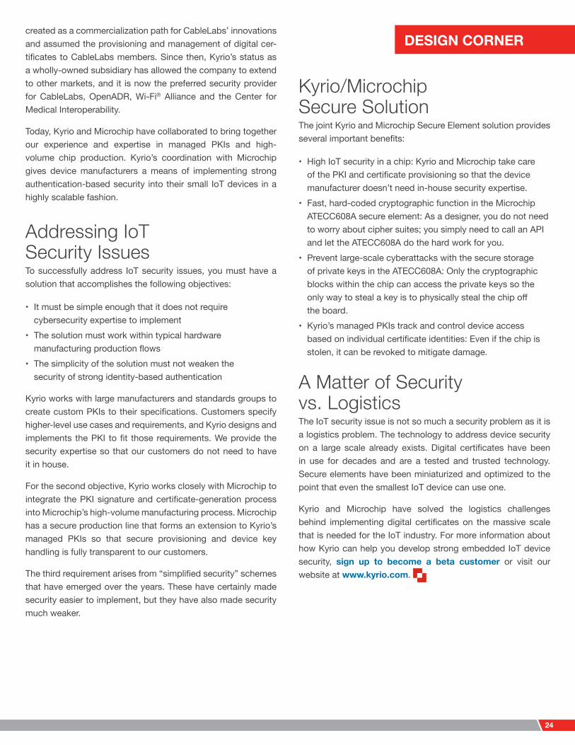
In his IoT security series published on the Kyrio blog, Ron Ih, Director of Business Development, has highlighted that even though encryption prevents eavesdropping, it does not iden-tify with whom you are communicating. If you cannot confirm identity, encryption becomes much less meaningful. The ability to verify the identity of whom you are communicating with is known as authentication, which is the cornerstone of any robust network security scheme.
Establishing Identity with Digital CertificatesDigital certificates are generated and cryptographically signed through a secure back-end system known as a Public Key Infra-structure (PKI). You can think of a managed PKI as the gov-ernment passport service and digital certificates as passports that devices use to verify their identities. A managed PKI has a certificate policy that is enforced by the Certificate Authority (CA). There are firm requirements for how certificates are issued and who can receive them, and even for signing authorized executable code.
Imagine that you could obtain a passport from anyone—with little or no control over how and to whom passports are issued. If that were the case, the passport loses meaning because it no longer proves anything. You have no way of knowing whether the passport is genuine. This is what you have if you use an unmanaged PKI.
Innovations from Kyrio, CableLabs and MicrochipIn 2001, CableLabs deployed one of the first large-scale autonomous device ecosystems using a managed PKI. Digital certificates were issued to verify compliance of cable modems and set-top boxes to adhere to the DOCSIS® communication standards, authenticate user subscriptions and ensure only authorized devices accessed the network. In 2012, Kyrio was
Encryption only prevents eavesdropping by malicious players. It doesn’t solve the problem of knowing who is on the other end of the communication line.
Managed PKIs with Microchip Secure ElementsContributed by Kyrio
DESIGN CORNER
24
created as a commercialization path for CableLabs’ innovations and assumed the provisioning and management of digital cer-tificates to CableLabs members. Since then, Kyrio’s status as a wholly-owned subsidiary has allowed the company to extend to other markets, and it is now the preferred security provider for CableLabs, OpenADR, Wi-Fi® Alliance and the Center for Medical Interoperability.
Today, Kyrio and Microchip have collaborated to bring together our experience and expertise in managed PKIs and high- volume chip production. Kyrio’s coordination with Microchip gives device manufacturers a means of implementing strong authentication-based security into their small IoT devices in a highly scalable fashion.
Addressing IoT Security IssuesTo successfully address IoT security issues, you must have a solution that accomplishes the following objectives:
• It must be simple enough that it does not require cybersecurity expertise to implement
• The solution must work within typical hardware manufacturing production flows
• The simplicity of the solution must not weaken the security of strong identity-based authentication
Kyrio works with large manufacturers and standards groups to create custom PKIs to their specifications. Customers specify higher-level use cases and requirements, and Kyrio designs and implements the PKI to fit those requirements. We provide the security expertise so that our customers do not need to have it in house.
For the second objective, Kyrio works closely with Microchip to integrate the PKI signature and certificate-generation process into Microchip’s high-volume manufacturing process. Microchip has a secure production line that forms an extension to Kyrio’s managed PKIs so that secure provisioning and device key handling is fully transparent to our customers.
The third requirement arises from “simplified security” schemes that have emerged over the years. These have certainly made security easier to implement, but they have also made security much weaker.
Kyrio/Microchip Secure Solution The joint Kyrio and Microchip Secure Element solution provides several important benefits:
• High IoT security in a chip: Kyrio and Microchip take care of the PKI and certificate provisioning so that the device manufacturer doesn’t need in-house security expertise.
• Fast, hard-coded cryptographic function in the Microchip ATECC608A secure element: As a designer, you do not need to worry about cipher suites; you simply need to call an API and let the ATECC608A do the hard work for you.
• Prevent large-scale cyberattacks with the secure storage of private keys in the ATECC608A: Only the cryptographic blocks within the chip can access the private keys so the only way to steal a key is to physically steal the chip off the board.
• Kyrio’s managed PKIs track and control device access based on individual certificate identities: Even if the chip is stolen, it can be revoked to mitigate damage.
A Matter of Security vs. LogisticsThe IoT security issue is not so much a security problem as it is a logistics problem. The technology to address device security on a large scale already exists. Digital certificates have been in use for decades and are a tested and trusted technology. Secure elements have been miniaturized and optimized to the point that even the smallest IoT device can use one.
Kyrio and Microchip have solved the logistics challenges behind implementing digital certificates on the massive scale that is needed for the IoT industry. For more information about how Kyrio can help you develop strong embedded IoT device security, sign up to become a beta customer or visit our website at www.kyrio.com.

COLORING PAGE
The Microchip name and logo and the Microchip logo are registered trademarks of Microchip Technology Incorporated in the U.S.A. and other countries. All other trademarks are the property of their registered owners. © 2017 Microchip Technology Inc. All rights reserved. 10/17DS20005875A
www.microchip.com/Serial-Number-EEPROM
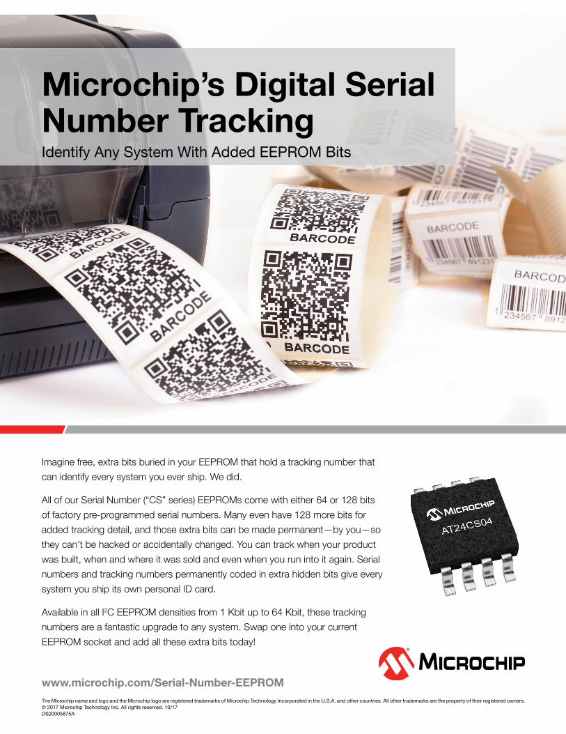
Microchip’s Digital Serial Number TrackingIdentify Any System With Added EEPROM Bits
Imagine free, extra bits buried in your EEPROM that hold a tracking number that can identify every system you ever ship. We did.
All of our Serial Number (“CS” series) EEPROMs come with either 64 or 128 bits of factory pre-programmed serial numbers. Many even have 128 more bits for added tracking detail, and those extra bits can be made permanent—by you—so they can’t be hacked or accidentally changed. You can track when your product was built, when and where it was sold and even when you run into it again. Serial numbers and tracking numbers permanently coded in extra hidden bits give every system you ship its own personal ID card.
Available in all I2C EEPROM densities from 1 Kbit up to 64 Kbit, these tracking numbers are a fantastic upgrade to any system. Swap one into your current EEPROM socket and add all these extra bits today!