luenberger disturbance observer-based deadbeat ... - mdpi
TRANSCRIPT
Citation: Yu, X.; Yang, Y.; Xu, L.; Ke,
D.; Zhang, Z.; Wang, F. Luenberger
Disturbance Observer-Based
Deadbeat Predictive Control for
Interleaved Boost Converter.
Symmetry 2022, 14, 924. https://
doi.org/10.3390/sym14050924
Academic Editor: Jan Awrejcewicz
Received: 30 March 2022
Accepted: 26 April 2022
Published: 1 May 2022
Publisher’s Note: MDPI stays neutral
with regard to jurisdictional claims in
published maps and institutional affil-
iations.
Copyright: © 2022 by the authors.
Licensee MDPI, Basel, Switzerland.
This article is an open access article
distributed under the terms and
conditions of the Creative Commons
Attribution (CC BY) license (https://
creativecommons.org/licenses/by/
4.0/).
symmetryS S
Article
Luenberger Disturbance Observer-Based Deadbeat PredictiveControl for Interleaved Boost ConverterXinhong Yu 1, Yumin Yang 1,2, Libin Xu 1,2, Dongliang Ke 1, Zhenbin Zhang 3 and Fengxiang Wang 1,2,*
1 Quanzhou Institute of Equipment Manufacturing, Haixi Institutes, Chinese Academy of Sciences,Quanzhou 362200, China; [email protected] (X.Y.); [email protected] (Y.Y.);[email protected] (L.X.) [email protected] (D.K.)
2 College of Electrical Engineering and Automation, Fuzhou University, Fuzhou 350108, China3 School of Electrical Engineering, Shandong University, Jinan 250100, China; [email protected]* Correspondence: [email protected]; Tel.:+86-0595-68187918
Abstract: A cascaded deadbeat predictive control strategy with online disturbance compensation isproposed for a three-phase interleaved boost converter in this paper. The topology of the three-phaseinterleaved converter is symmetric, so the inner loop controller is also designed symmetrically. For thepurpose of realizing the error-free tracking of reference value, the deadbeat predictive control methodis adopted for inner and outer loops with Luenberger observers, which are designed to estimateand compensate the disturbances of load variation in the power model as well as the unknownresistor of inductance in the current model. To eliminate the influence of a time delay, a two-steppredictive control method is adopted in the predictive model. In the aspect of parameter design, thepole placement method is adopted to determine the gain of the observer. A series of simulations andexperiments are carried out to test the proposed strategy under steady and dynamic conditions. Itis shown that the proposed control strategy has faster dynamic response and stronger robustnessagainst disturbance than the conventional model predictive control.
Keywords: interleaved boost converter; cascaded deadbeat predictive control; Luenberger observer;online disturbance compensation
1. Introduction
Boost converters, relying on their energy conversion, regulation, and other functions,have been widely used in fuel cell vehicle power systems [1], photovoltaic cells [2,3], UPS,energy storage systems, etc. In recent years, since the rapid development of the abovefields, the performance of boost converter is increasingly required to have better powerdensity, dynamic response capability, stability, reliability and so on.
Because of the increasing demand for equipment capacity and power levels, thereliability of power devices in traditional DC–DC converters faces great challenges. Whenthe input current ripple of the converter is large, the service life of the battery systemwill be affected. Meanwhile, in order to solve the problem of device stress when theconverters are applied in high-power occasions, scholars have improved the topology byintroducing interleaved [4], multi-level technology [5], etc. For high-power situations witha high current requirement, such as grid-connected inverters [6], power factor correction(PFC) [7,8], and voltage regulator modules [9], interleaved technology is currently themost popular solution. When boost converters are working under continuous currentmode (CCM), there is a right half-plane zero (RHP zero) in the open-loop transfer function.This proves that the boost converter belongs to the non-minimum phase system, whichtherefore reduces the dynamic performance of the converter [10]. Current-mode control,a widely used method, contains faster response and a larger bandwidth compared withthe conventional voltage-mode control [11]. Although the classical proportional-integral(PI) controller has been widely used in most control systems, the gain of the PI controller
Symmetry 2022, 14, 924. https://doi.org/10.3390/sym14050924 https://www.mdpi.com/journal/symmetry
Symmetry 2022, 14, 924 2 of 17
is difficult to determine. In addition, the fixed gain coefficient is not suitable for alloperating conditions.
Since the 21st century, model predictive control (MPC), as a typical representative ofthe advanced process control algorithm, has achieved all-round development and rapidlyextended its application field. MPC is famous for its simple principle, fast response speed,and its ability to deal with non-linear systems as well as multivariable constraints. It hasbeen widely studied by scholars as a promising control strategy and used in the controlof power electronics and electric drive in recent years [12,13]. However, the effectivenessof MPC is largely dependent on the accuracy of system modeling. Due to the various andunpredictable working conditions of the converter, both disturbances and uncertaintieswill result in adverse influences on the conventional MPC performance of the systems, suchas waveform distortion and slower dynamic response, as well as poor system stability. Inregard to boost converters, the most relevant elements are parameter mismatches, unknownchanges of the load and input voltage, as well as the existence of equivalent series resistance(ESR) in the inductance [2,14]. In order to ensure that the converter can obtain the desireddynamic response and stability, a lot of research related to enhancing the anti-interferenceability of the system has been proposed in the literature [15–24].
Observer adoption is one of the most direct and effective methods to estimate distur-bance and compensate for it online in control systems [15,25]. In [16], the robust controllerbased on the extended state observer is compared with the conventional PI controller inthe aspect of compensation. The study shows that the integral could act as an observer tocompensate for the effect of disturbance as well as the proportional, which could strengthenthe accuracy of tracking accuracy in steady state and accelerate the transient response.Overall, the robust controller has superior performance.
The finite control set MPC (FCS-MPC), is adopted in [17–19]. It is a four-order slidingmode observer based on an extended state model that was introduced in [18] to observe theoutput current and the input voltage. In [19], an observer-based modified model is used toreplace the original model to overcome the model mismatches. However, the FCS-MPC is avariable frequency control, which increases the difficulty of the design of the filter.
The continuous control set MPC (CCS-MPC) strategy is adopted in [20–24]. In [21], itis indicated that the steady-state error of the boost converter still exists in spite of using aPI controller to correct the voltage in current sensorless predictive control. By analyzing thesmall-signal model with parasitic parameters, a self-correction differential current observeris introduced to eliminate the steady-state error. But the process of small signal analysisand the design of the compensation net are complicated. In [22], to improve the accuracy,a sensorless explicit MPC scheme is introduced by using an extended Kalman filter toestimate the noise of measurement. However, the heavy calculation burden results inthe need for an offline process to tune the parameters. Furthermore, the PI controller isstill required for the voltage-loop control to compensate for the effects of the parasiticparameters and the existence of integrator; this, therefore, reduces the dynamic response.
In this paper, the model predictive control strategy of three-phase interleaved boostconverter (IBC) is studied. A cascaded deadbeat predictive control strategy based on onlinedisturbance compensation is designed. The strategy adopts deadbeat predictive controlin both inner and outer loops. Considering the symmetry of the topology, the inner loopcontroller can be designed symmetrically from a single phase. The load of the power modeland the lumped disturbance of the current model are estimated in real time by a Luenbergerdisturbance observer. Then it is compensated to the prediction model online by designing aLuenberger disturbance observer (LDO). A two-step predictive control method is adoptedin the predictive model to eliminate the effect of the time delay. For the configuration of theobserver gain coefficient, the closed-loop pole distribution trajectory of the current observerwas analyzed and the self-correcting gain under various working conditions was designedto accelerate the dynamic convergence rate of the observation error. The proposed methodimproves the robustness of the system and has faster dynamic response. Simulation andexperimental results prove the effectiveness of the proposed strategy.
Symmetry 2022, 14, 924 3 of 17
This article is organized as follows. In Section 2, a mathematical model of IBC ispresented. In Section 3, the proposed control method is designed based on the Luenbergerobserver as well as a two-step predictive model with the analysis of parameters tuning. InSection 4, the simulation and experiment results of conventional method and proposedmethod are given and analyzed. Finally, Section 5 concludes this article.
2. Model of the Interleaved Boost Converter
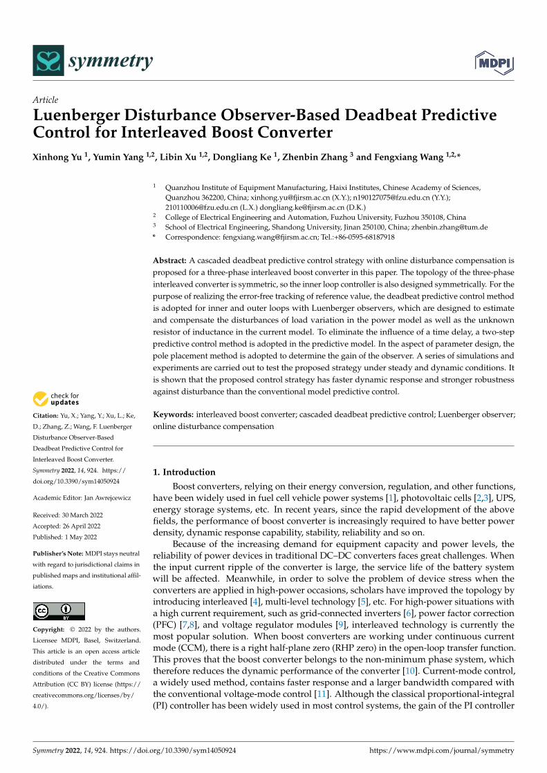
The topology of the main circuit is shown in Figure 1 to increase the power level.The three-phase IBC has three identical boost converters in parallel, where Vin stands forinput source voltage, Vo for output voltage, Ro for equivalent load resistance and C f foroutput capacitor. Each branch is composed of a controllable switch Si (i = 1, 2, 3), a diodeDi (i = 1, 2, 3) and an inductance Li (i = 1, 2, 3) with ESR RLi (i = 1, 2, 3).
3L
2L
1L
3LR
2LR
1LR
3D
2D
1D
1S 2S 3SfC oRinV
+
−oV
+
−
Figure 1. The topology of the three-phase IBC.
Because the proposed scheme is based on the CCS-MPC method, both the continuousand discrete time models need to be built to present the dynamic of the systems. Assumingthat the converter is operating under CCM. on the basis of the Kirchhoff’s Law and thestate-space averaging method [26], continuous-time model is expressed as follows:
diLi(t)dt
=Vin − iLi(t)RLi
Li− Vo(t)
Li[1− ui(t)]
dVo(t)dt
=3
∑i=1
iLi(t)C f
[1− ui(t)]−Vo(t)C f Ro
(i = 1, 2, 3), (1)
where ui(t) is the input of the system which stands for the duty cycle of the switch Si (i =1, 2, 3) respectively, and iLi is the inductance current.
A four-order system model, which is comprised of the state vectors, is applied on theconverter. The states variable is defined as x(t) = [ x1 x2 x3 x4 ]T = [ iLI iL2 iL3 Vo ]T . Thus thediscrete time model of the converter is presented as:
x(k + 1) = Ax(k) + B[x(k)]U + Evy(k) = Cx(k)
, (2)
where Ts is the sampling time, v = Vin, A =
1− TsRL1
L10 0 − Ts
L1
0 1− TsRL2L2
0 − TsL2
0 0 1− TsRL3L3
− TsL3
TsC f
TsC f
TsC f
1− TsC f Ro
,
E =
TsL1TsL2TsL30
, C =
1 0 0 00 1 0 00 0 1 00 0 0 1
, B =
TsL1
Vo(k) 0 00 Ts
L2Vo(k) 0
0 0 TsL3
Vo(k)− Ts
C fiL1(k) − Ts
C fiL2(k) − Ts
C fiL3(k)
, and
Symmetry 2022, 14, 924 4 of 17
U =
u1(k)u2(k)u3(k)
.
3. Controller Design
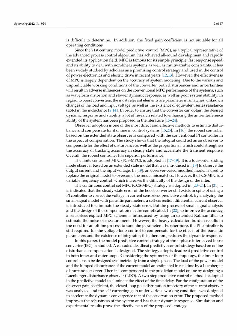
A cascaded deadbeat predictive control strategy with online disturbance compensationfor IBC is designed in this section. Because the boost converter belongs to a non-minimumphase system, to control the output voltage in a one-step prediction, controlling the induc-tance current should be placed in the first place. The control block diagram of the proposedcontrol strategy is presented in Figure 2.
CPS-PWMcost functionpower equilibrium*Li [ ]i ku
iS
load LDOIBC
[ 2]pLi ki +
current predictive model
lump disturbance LDO
current predictive model
lump disturbance LDO[ ]o kV [ ]in kV
ˆoR
[ ]ˆi kD [ ]o kV
[ ]Li ki
[ ]i ku
Figure 2. Control diagram of LDO-MPC.
For the conventional deadbeat predictive control method, the load resistance Ro andthe input source voltage Vin are generally regarded as time-invariant and known, and theequivalent series resistance RLi (i = 1, 2, 3) is neglected. However, in most application areas,the Ro and Vin always vary in an unknown manner and the existence of RLi (i = 1, 2, 3)makes the modeling imprecise. As a result, it leads to model mismatches, a steady-stateerror of output voltage and the deterioration of robustness and dynamic performance.Therefore, LDOs are designed to solve the above problem respectively in this work.
3.1. Design of the Voltage Loop3.1.1. Steady-State Inductance Current Reference
In the outer loop, it is supposed that the switching loss is ignored. Then the referencevalue of the inductance current was calculated based on the theory of power equilibrium,which is expressed as
viniin = C fdVo
dtVo(t) +
V2o (t)Ro
, (3)
where the value on the left side of the equal sign represents the input power of the converter,the first term on the right side of the equal sign represents the power absorbed by capacitorstorage, and the second term represents the power consumed on the load.
Equation (3) is discretized to obtain a discrete power state equation. By appointing theoutput voltage at k + 1 equal to the reference output V∗o , the input current reference i∗in ofthe converter is obtained:
i∗in =C f Vo(t)
TsVin[V∗o −Vo(k)] +
V2o (k)
VinRo. (4)
The digital controlled current-sharing method is adopted. In order to ensure three-phase branch currents are equal, the reference current value i∗Li of each phase is defined asone-third of the reference value i∗in as follows:
i∗Li =13
i∗in =C f Vo(k)3TsVin
[V∗o −Vo(k)] +V2
o (k)3VinRo
(i = 1, 2, 3). (5)

Symmetry 2022, 14, 924 5 of 17
3.1.2. Observation of the Load Resistance Ro
According to (5), the load resistance Ro is needed when calculating the referencei∗Li, so the observer is designed to observe the load without using the current sensor. Asmentioned above, Vo(t) is measurable whereas Ro(t) is unmeasurable, and the model ofthe system (1) can be written as
Vo(k + 1) = (1− Ts
RoC f)Vo(k) +
Ts
C f
VinVo(k)
iin(k)
Ro(k + 1) = Ro(k).(6)
Set output voltage Vo and load resistance as state variables, and the discrete Luenbergerobserver can be designed in the following form:
Vo(k + 1) = (1− Ts
RoC f)Vo(k) +
Ts
C f
Vin
Vo(k)iin(k) + L2[Vo(k)− Vo(k)]
Ro(k + 1) = Ro(k) + L1[Vo(k)− Vo(k)],(7)
where L1 and L2 stands for the observer gain.
3.2. Design of the Current Loop3.2.1. Design of the MPC
Assuming that the input voltage Vin and output voltage Vo are kept unchanged duringa sampling period, the inductance current is changing in a linear fashion. Based onEquation (1) and the forward Euler method, the inductance current ip
Li(k + 1)(i = 1, 2, 3) atk + 1 step, which is deduced from time k, is calculated as follows:
ipLi(k + 1) = (1− TsRLi
Li)iLi(k)−
Ts
Li[1− ui(k)]Vo(k) +
Ts
LiVin(k) (i = 1, 2, 3). (8)
Based on the predictive model, the proposed dead-beat control is designed. The costfunction can be designed as [27,28]:
g =3
∑i=1
[i∗Li − ip
Li(k + 1)]2
(i = 1, 2, 3). (9)
From (9), the optimal ipLi(k + 1) can be obtained by solving ∂g
∂u1(k)= 0, ∂g
∂u2(k)= 0 and
∂g∂u3(k)
= 0 to minimize g based on the deadbeat predictive control theory. The duty cycle iscalculated as
ui(k) = 1 +L
Vo(k)Ts[i∗Li − iLi(k)] +
RLiiLi(k)−Vin(k)Vo(k)
(i = 1, 2, 3). (10)
3.2.2. Observation of the Lumped Disturbance Di (i = 1, 2, 3)
According to (1), the lumped disturbance term can be expressed as
Di(t) =Vin − iLi(t)RLi
Li(i = 1, 2, 3). (11)
In this paper, the state variables iLi(t) (i = 1, 2, 3) are measurable, whereas Di(t) (i =1, 2, 3) is unknown. Assuming the value of Di(t) and Vo(t) are constant in one samplingperiod, the equation of state can be written as
Xdi(k + 1) = AdXdi(k) + Bdiui(k) + Edivd
Ydi(k + 1) = CdXdi(k + 1),(12)
Symmetry 2022, 14, 924 6 of 17
where Xdi(k) = [ iLi Di ]T , Cd = [ 1 0 ], Ad = [ 1 Ts0 1 ], Edi = [ − Ts
Li0 ]T , Bdi = [ TsVo(k)
Li0 ]T and
vd = Vo. So the LDO is described as follows:Xdi(k + 1) = AdXdi(k) + Bdiui(k) + Edivd + H[Ydi(k)− Ydi(k)]Ydi(k + 1) = CdXdi(k + 1),
(13)
where H = [ h1 h2 ]T is a designed 2× 1 dimension constant matrix.According to (12) and (13), the error of the state variable and the observed value at
time k + 1 is defined as
Xdi(k + 1) = Xdi(k + 1)− Xdi(k + 1) = (Ad −HCd)[Xdi(k)− Xdi(k)]. (14)
3.3. Time Delay
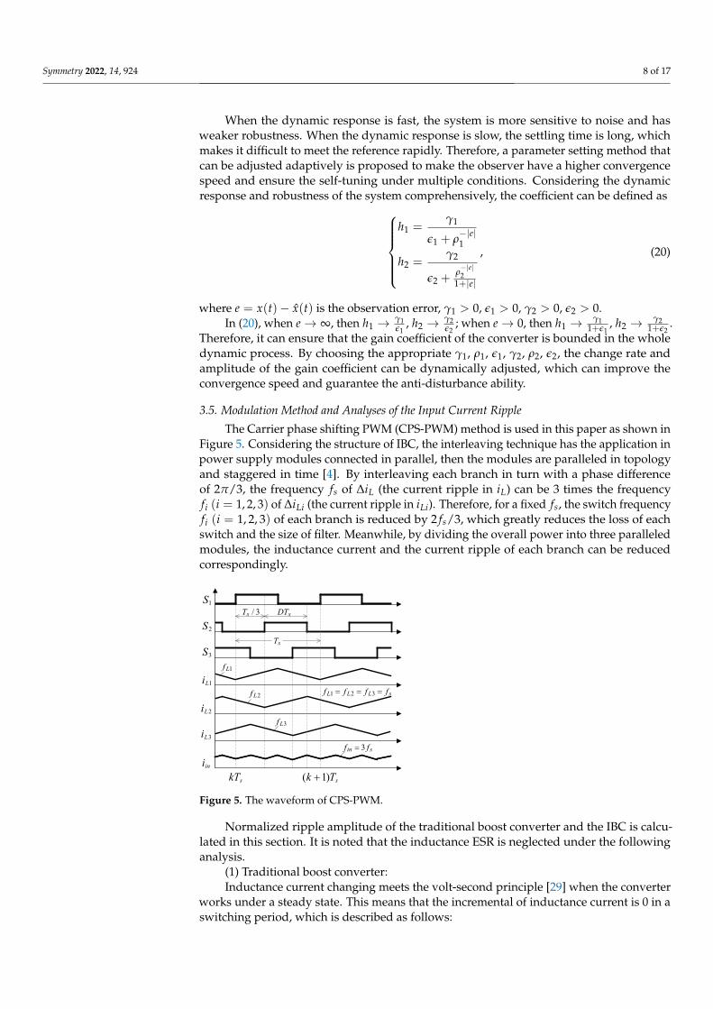
The system has inertial elements such as inductance and low-pass filters, as well asthe sampling and modulation processes. These will result in an inherent delay for twocycles. When the duty cycle D acted on the system at k− 1, the corresponding current wassampled at k by ADC module. Then the duty cycle D at k only can be output by CPS-PWMat k + 1. If the time delay problem is not considered when designing the controller, thecontrol performance of the system may deteriorate, such as the increase of the ripple. Inorder to avoid the inherent delay, this affects the accurate prediction of voltage and current.In this paper, a two-step prediction is used to compensate the inherent delay, and the time-sequence between the system state variable x(t) and the input u(t) after the time-delaycompensation is shown in Figure 3.
apply to the system
sample
apply to the system
sample
iS t
t
( 2)u k +
( )x k ( 1)x k + ( 2)x k +
( 3)u k +
Data Processing
( )u k
( )x k
( 1)u k +
( 1)x k +
( 2)u k +
( 2)x k +
( 1)u k +
Lii
k 1k + 2k +
( )u k ( 1)u k + ( 2)u k +
Algorithm
Output
Voltage
Pulse
apply to the system
sample
Figure 3. Timing sequence between the state variable and the input variable.
The following delay compensator is designed to improve the predictive model:x(k + 1) = Ax(k) + B[x(k)]U(k) + Evx(k + 2) = Ax(k + 1) + B[x(k + 1)]U(k + 1) + Ev
, (15)
where x(k), x(k + 1), x(k + 2) stand for the system state variables at k, k + 1, k + 2 respec-tively, and the cost function (9) is rewritten as follows:
J = [i∗L1 − ipL1(k + 2)]2 + [i∗L2 − ip
L2(k + 2)]2 + [i∗L3 − ipL3(k + 2)]2. (16)
3.4. Observer Stability Analysis and Parameters Tuning
In the above sections, a cascade deadbeat predictive control strategy based on anon-line compensation of disturbance is proposed. The observer gain coefficient is usuallydesigned as a fixed value, which only needs to satisfy that the matrix (Ad −HCd) is aHurwitz matrix to ensure the stability of the observer. The fixed value is given accordingto engineering practice. It relies heavily on experience and cannot be compatible with allworking conditions. An optimal design of the observer gain coefficient of the inner loop
Symmetry 2022, 14, 924 7 of 17
is given in this section so that it can update the value of the parameters according to thereal-time feedback data.
According to Equation (14), the characteristic equation can be written as follows:
D(z) = |zI− (Ad −HCd)| = p2z2 + p1z + p0, (17)
where p2 = 1, p1 = h1 − 2, p0 = 1− h1 + h2Ts.According to Jury stability criterion in the discrete domain, the roots of the characteris-
tic equation must be located in the unit circle to ensure asymptotic stability of the observer.Therefore, the following requirements must be satisfied:
D(1) > 0
(−1)nD(−1) > 0
|p0| < pn
, (18)
where n = 2 according to (17).On the basis of (18), a feasible range of the gain coefficient h1 and h2 is calculated as
h2Ts < h1 < 2 +h2Ts
2
0 < h1 <4Ts
(19)
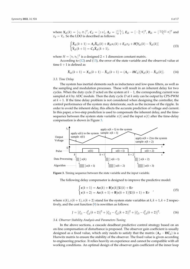
The gain coefficients can be further adjusted by plotting and analyzing the trajectoriesof the closed-loop pole distributions. As shown in Figure 4, there are 4 groups in total, andthe values of h1 are 0.2, 0.3, 0.4, 0.5 respectively, and h2 increases from 100 to 1000 with 100as the step length.
When h1 is fixed and h2 increases, the poles move away from the real axis at first.This means that the dynamic response of the system slows down, the damping coefficientdecreases, and the overshoot increases. When h2 continues to increase until the polesbecome conjugate poles, that is, moving away from the real axis to both sides, the dynamicresponse continues to slow down. Then oscillations occurred as the poles graduallyapproach the boundary of the unit circle.
When h2 is fixed as a small value and h1 increases, the poles first move to the negativedirection of the real axis, the dynamic response of the system becomes faster, the dampingcoefficient increases, and the overshoot decreases. When h2 is large and h1 increases, thepoles move to both sides of the real axis, and the dynamic response slows down.
Real axis
Imag
inary
ax
is
Figure 4. Closed-loop pole distribution trajectory when gain coefficient changes.
Symmetry 2022, 14, 924 8 of 17
When the dynamic response is fast, the system is more sensitive to noise and hasweaker robustness. When the dynamic response is slow, the settling time is long, whichmakes it difficult to meet the reference rapidly. Therefore, a parameter setting method thatcan be adjusted adaptively is proposed to make the observer have a higher convergencespeed and ensure the self-tuning under multiple conditions. Considering the dynamicresponse and robustness of the system comprehensively, the coefficient can be defined as
h1 =γ1
ε1 + ρ−|e|1
h2 =γ2
ε2 +ρ−|e|2
1+|e|
, (20)
where e = x(t)− x(t) is the observation error, γ1 > 0, ε1 > 0, γ2 > 0, ε2 > 0.In (20), when e→ ∞, then h1 → γ1
ε1, h2 → γ2
ε2; when e→ 0, then h1 → γ1
1+ε1, h2 → γ2
1+ε2.
Therefore, it can ensure that the gain coefficient of the converter is bounded in the wholedynamic process. By choosing the appropriate γ1, ρ1, ε1, γ2, ρ2, ε2, the change rate andamplitude of the gain coefficient can be dynamically adjusted, which can improve theconvergence speed and guarantee the anti-disturbance ability.
3.5. Modulation Method and Analyses of the Input Current Ripple
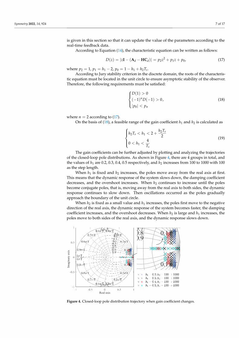
The Carrier phase shifting PWM (CPS-PWM) method is used in this paper as shown inFigure 5. Considering the structure of IBC, the interleaving technique has the application inpower supply modules connected in parallel, then the modules are paralleled in topologyand staggered in time [4]. By interleaving each branch in turn with a phase differenceof 2π/3, the frequency fs of ∆iL (the current ripple in iL) can be 3 times the frequencyfi (i = 1, 2, 3) of ∆iLi (the current ripple in iLi). Therefore, for a fixed fs, the switch frequencyfi (i = 1, 2, 3) of each branch is reduced by 2 fs/3, which greatly reduces the loss of eachswitch and the size of filter. Meanwhile, by dividing the overall power into three paralleledmodules, the inductance current and the current ripple of each branch can be reducedcorrespondingly.
1S
2S
3S
1Li
2Li
3Li
ini
skT ( 1) sk T+
1Lf
2Lf 1 2 3L L L sf f f f= = =
3Lf
3in sf f=
sT
sDT/ 3sT
Figure 5. The waveform of CPS-PWM.
Normalized ripple amplitude of the traditional boost converter and the IBC is calcu-lated in this section. It is noted that the inductance ESR is neglected under the followinganalysis.
(1) Traditional boost converter:Inductance current changing meets the volt-second principle [29] when the converter
works under a steady state. This means that the incremental of inductance current is 0 in aswitching period, which is described as follows:
Symmetry 2022, 14, 924 9 of 17
∆iL+ = ∆iL−
∆iL+ =VinL
DTs
∆iL− =Vo −Vin
L(1− D)Ts
, (21)
where Ts is the switching period and D is duty cycle.The ripple amplitude of the traditional boost converter is obtained as
∆iL =Vo
L fsD(1− D). (22)
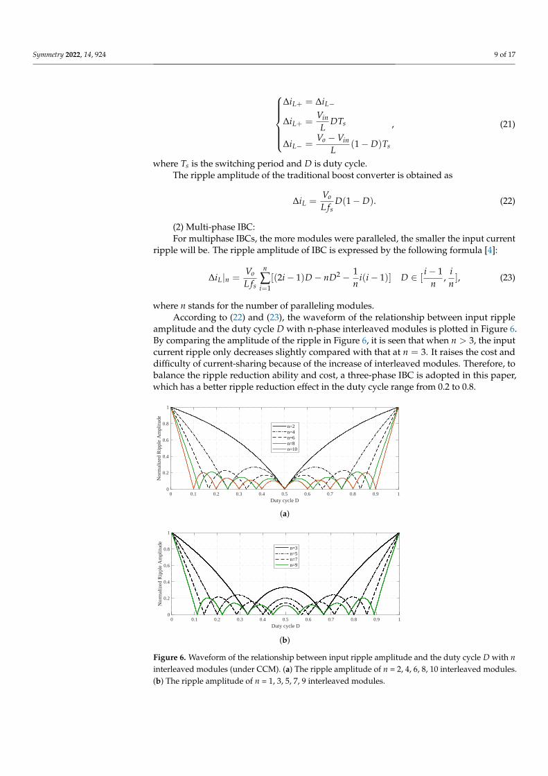
(2) Multi-phase IBC:For multiphase IBCs, the more modules were paralleled, the smaller the input current
ripple will be. The ripple amplitude of IBC is expressed by the following formula [4]:
∆iL|n =Vo
L fs
n
∑i=1
[(2i− 1)D− nD2 − 1n
i(i− 1)] D ∈ [i− 1
n,
in], (23)
where n stands for the number of paralleling modules.According to (22) and (23), the waveform of the relationship between input ripple
amplitude and the duty cycle D with n-phase interleaved modules is plotted in Figure 6.By comparing the amplitude of the ripple in Figure 6, it is seen that when n > 3, the inputcurrent ripple only decreases slightly compared with that at n = 3. It raises the cost anddifficulty of current-sharing because of the increase of interleaved modules. Therefore, tobalance the ripple reduction ability and cost, a three-phase IBC is adopted in this paper,which has a better ripple reduction effect in the duty cycle range from 0.2 to 0.8.
0 0.1 0.2 0.3 0.4 0.5 0.6 0.7 0.8 0.9 1Duty cycle D
0
0.2
0.4
0.6
0.8
1
Nor
mal
ized
Rip
ple
Am
plitu
de
n=2n=4n=6n=8n=10
(a)
0 0.1 0.2 0.3 0.4 0.5 0.6 0.7 0.8 0.9 1Duty cycle D
0
0.2
0.4
0.6
0.8
1
Nor
mal
ized
Rip
ple
Am
plitu
de
n=3n=5n=7n=9
(b)
Figure 6. Waveform of the relationship between input ripple amplitude and the duty cycle D with ninterleaved modules (under CCM). (a) The ripple amplitude of n = 2, 4, 6, 8, 10 interleaved modules.(b) The ripple amplitude of n = 1, 3, 5, 7, 9 interleaved modules.
Symmetry 2022, 14, 924 10 of 17
4. Simulation and Experiment Results
The simulations and experiments are carried out in this section. To evaluate thecorrectness and effectiveness of the proposed control strategy, simulations and experimentsare implemented for LDO-MPC and PI-MPC under several operating conditions. Thecorresponding main circuit parameters are listed in Table 1.
Table 1. Nominal Simulation Parameter of the Circuit.
Descriptions Symbol Values
Output voltage Vo 400 VInput voltage Vin 200 V
Inductance L1, L2, L3 1 mHInductance resistor RL1, RL2, RL3 0.3 Ω
Load resistor Ro 10 ΩInput capacitor Cin 2000 µF
Output capacitor C f 4000 µFSwitching frequency fs 10 kHz
4.1. Simulation Results4.1.1. Step Changes in the Output Voltage Reference
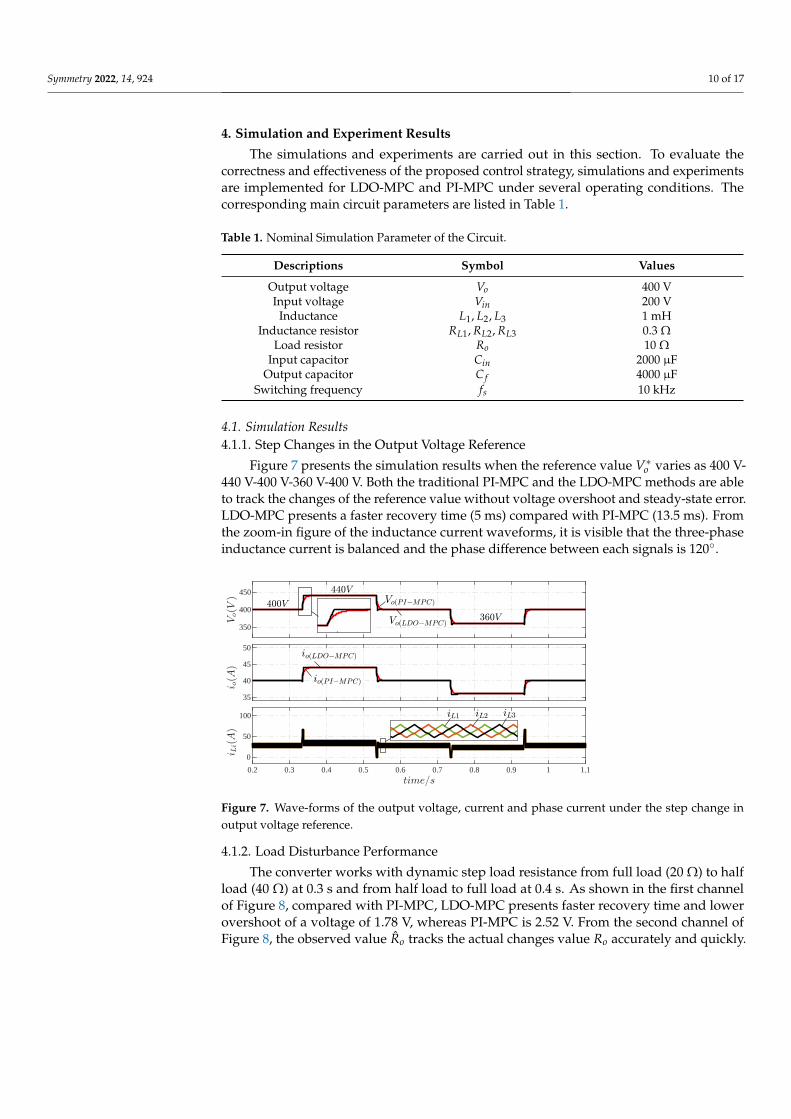
Figure 7 presents the simulation results when the reference value V∗o varies as 400 V-440 V-400 V-360 V-400 V. Both the traditional PI-MPC and the LDO-MPC methods are ableto track the changes of the reference value without voltage overshoot and steady-state error.LDO-MPC presents a faster recovery time (5 ms) compared with PI-MPC (13.5 ms). Fromthe zoom-in figure of the inductance current waveforms, it is visible that the three-phaseinductance current is balanced and the phase difference between each signals is 120.
350
400
450
35
40
45
50
0.2 0.3 0.4 0.5 0.6 0.7 0.8 0.9 1 1.1
0
50
100
Figure 7. Wave-forms of the output voltage, current and phase current under the step change inoutput voltage reference.
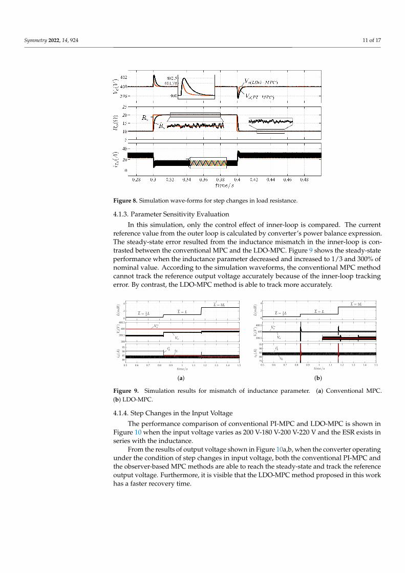
4.1.2. Load Disturbance Performance
The converter works with dynamic step load resistance from full load (20 Ω) to halfload (40 Ω) at 0.3 s and from half load to full load at 0.4 s. As shown in the first channelof Figure 8, compared with PI-MPC, LDO-MPC presents faster recovery time and lowerovershoot of a voltage of 1.78 V, whereas PI-MPC is 2.52 V. From the second channel ofFigure 8, the observed value Ro tracks the actual changes value Ro accurately and quickly.
Symmetry 2022, 14, 924 11 of 17
Figure 8. Simulation wave-forms for step changes in load resistance.
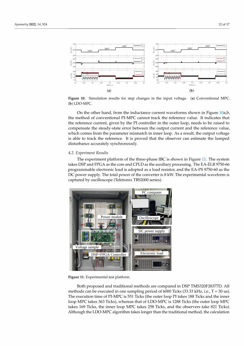
4.1.3. Parameter Sensitivity Evaluation
In this simulation, only the control effect of inner-loop is compared. The currentreference value from the outer loop is calculated by converter’s power balance expression.The steady-state error resulted from the inductance mismatch in the inner-loop is con-trasted between the conventional MPC and the LDO-MPC. Figure 9 shows the steady-stateperformance when the inductance parameter decreased and increased to 1/3 and 300% ofnominal value. According to the simulation waveforms, the conventional MPC methodcannot track the reference output voltage accurately because of the inner-loop trackingerror. By contrast, the LDO-MPC method is able to track more accurately.
0
2
4
10-3
399
399.5
400
400.5
0.5 0.6 0.7 0.8 0.9 1 1.1 1.2 1.3 1.4 1.5
80
85
90
95
(a)
0
2
4
10-3
399.5
400
400.5
0.5 0.6 0.7 0.8 0.9 1 1.1 1.2 1.3 1.4 1.5
75
80
85
90
95
(b)
Figure 9. Simulation results for mismatch of inductance parameter. (a) Conventional MPC.(b) LDO-MPC.
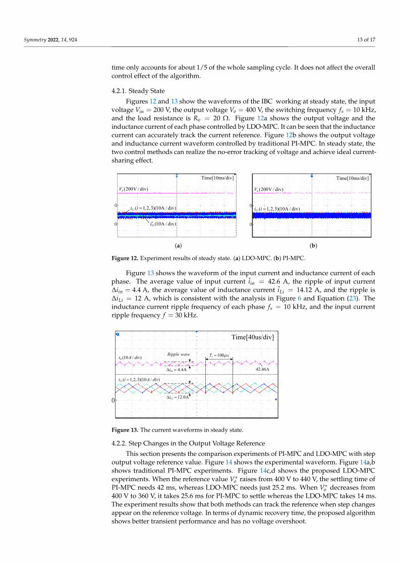
4.1.4. Step Changes in the Input Voltage
The performance comparison of conventional PI-MPC and LDO-MPC is shown inFigure 10 when the input voltage varies as 200 V-180 V-200 V-220 V and the ESR exists inseries with the inductance.
From the results of output voltage shown in Figure 10a,b, when the converter operatingunder the condition of step changes in input voltage, both the conventional PI-MPC andthe observer-based MPC methods are able to reach the steady-state and track the referenceoutput voltage. Furthermore, it is visible that the LDO-MPC method proposed in this workhas a faster recovery time.
Symmetry 2022, 14, 924 12 of 17
150
200
250
398
400
402
0.3 0.35 0.4 0.45 0.5 0.55 0.6 0.65 0.7
70
80
90
100
(a)
150
200
250
398
400
402
0.3 0.35 0.4 0.45 0.5 0.55 0.6 0.65 0.7
70
80
90
100
(b)
Figure 10. Simulation results for step changes in the input voltage. (a) Conventional MPC.(b) LDO-MPC.
On the other hand, from the inductance current waveforms shown in Figure 10a,b,the method of conventional PI-MPC cannot track the reference value. It indicates thatthe reference current, given by the PI controller in the outer loop, needs to be raised tocompensate the steady-state error between the output current and the reference value,which comes from the parameter mismatch in inner loop. As a result, the output voltageis able to track the reference. It is proved that the observer can estimate the lumpeddisturbance accurately synchronously.
4.2. Experiment Results
The experiment platform of the three-phase IBC is shown in Figure 11. The systemtakes DSP and FPGA as the core and CPLD as the auxiliary processing. The EA-ELR 9750-66programmable electronic load is adopted as a load resistor, and the EA-PS 9750-60 as theDC power supply. The total power of the converter is 8 kW. The experimental waveform iscaptured by oscilloscope (Tektronix TBS2000 series).
Voltage sample
Power module
DSP+FPGA Controller Electronic load
DC power supply
PC computer
Oscilloscope
Figure 11. Experimental test platform.
Both proposed and traditional methods are compared in DSP TMS320F28377D. Allmethods can be executed in one sampling period of 6000 Ticks (33.33 kHz, i.e., T = 30 us).The execution time of PI-MPC is 551 Ticks (the outer loop PI takes 188 Ticks and the innerloop MPC takes 363 Ticks), whereas that of LDO-MPC is 1288 Ticks (the outer loop MPCtakes 169 Ticks, the inner loop MPC takes 258 Ticks, and the observers take 821 Ticks).Although the LDO-MPC algorithm takes longer than the traditional method, the calculation
Symmetry 2022, 14, 924 13 of 17
time only accounts for about 1/5 of the whole sampling cycle. It does not affect the overallcontrol effect of the algorithm.
4.2.1. Steady State
Figures 12 and 13 show the waveforms of the IBC working at steady state, the inputvoltage Vin = 200 V, the output voltage Vo = 400 V, the switching frequency fs = 10 kHz,and the load resistance is Ro = 20 Ω. Figure 12a shows the output voltage and theinductance current of each phase controlled by LDO-MPC. It can be seen that the inductancecurrent can accurately track the current reference. Figure 12b shows the output voltageand inductance current waveform controlled by traditional PI-MPC. In steady state, thetwo control methods can realize the no-error tracking of voltage and achieve ideal current-sharing effect.
( 1,2,3)(10A / div)Lii i =
* (10A / div)Lii
0
0
Time[10ms/div]
(200V / div)oV
(a)
( 1,2,3)(10A / div)Lii i =
(200V / div)oV
Time[10ms/div]
0
0
(b)
Figure 12. Experiment results of steady state. (a) LDO-MPC. (b) PI-MPC.
Figure 13 shows the waveform of the input current and inductance current of eachphase. The average value of input current iin = 42.6 A, the ripple of input current∆iin = 4.4 A, the average value of inductance current iLi = 14.12 A, and the ripple is∆iLi = 12 A, which is consistent with the analysis in Figure 6 and Equation (23). Theinductance current ripple frequency of each phase fs = 10 kHz, and the input currentripple frequency f = 30 kHz.
42.46A
( 1,2,3)(10 / )Lii i A div=
100sT s=
12.0ALii =
Ripple wave
4.4Aini =
Time[40us/div]
0
(10 / )ini A div
Figure 13. The current waveforms in steady state.
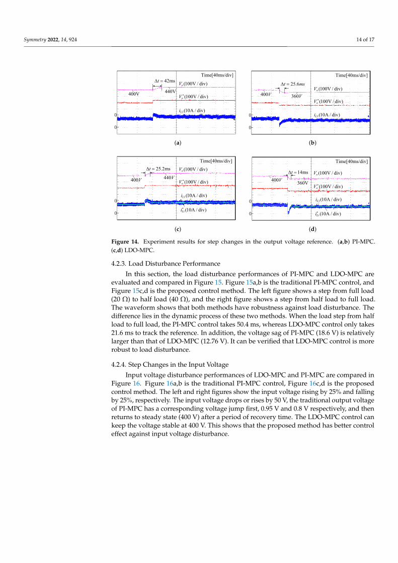
4.2.2. Step Changes in the Output Voltage Reference
This section presents the comparison experiments of PI-MPC and LDO-MPC with stepoutput voltage reference value. Figure 14 shows the experimental waveform. Figure 14a,bshows traditional PI-MPC experiments. Figure 14c,d shows the proposed LDO-MPCexperiments. When the reference value V∗o raises from 400 V to 440 V, the settling time ofPI-MPC needs 42 ms, whereas LDO-MPC needs just 25.2 ms. When V∗o decreases from400 V to 360 V, it takes 25.6 ms for PI-MPC to settle whereas the LDO-MPC takes 14 ms.The experiment results show that both methods can track the reference when step changesappear on the reference voltage. In terms of dynamic recovery time, the proposed algorithmshows better transient performance and has no voltage overshoot.
Symmetry 2022, 14, 924 14 of 17
400V440V
1(10A / div)Li
*(100V / div)oV
(100V / div)oV42mst =
0
0
Time[40ms/div]
(a)
400V 360V
1(10A / div)Li
*(100V / div)oV
(100V / div)oV25.6t ms =
0
0
Time[40ms/div]
(b)
400V440V
(100V / div)oV
*(100V / div)oV
1(10A / div)Li
* (10A / div)Lii
25.2mst =
0
0
Time[40ms/div]
(c)
360V400V
(100V / div)oV
*(100V / div)oV
1(10A / div)Li
* (10A / div)Lii
14mst =
0
0
Time[40ms/div]
(d)
Figure 14. Experiment results for step changes in the output voltage reference. (a,b) PI-MPC.(c,d) LDO-MPC.
4.2.3. Load Disturbance Performance
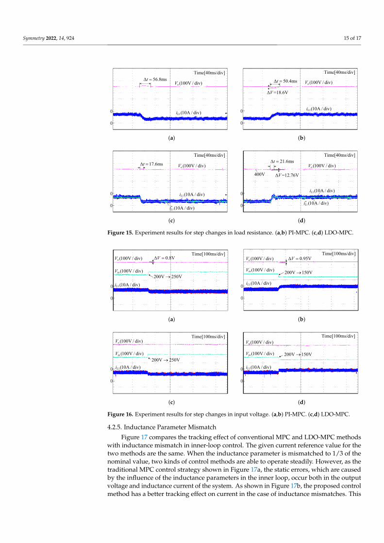
In this section, the load disturbance performances of PI-MPC and LDO-MPC areevaluated and compared in Figure 15. Figure 15a,b is the traditional PI-MPC control, andFigure 15c,d is the proposed control method. The left figure shows a step from full load(20 Ω) to half load (40 Ω), and the right figure shows a step from half load to full load.The waveform shows that both methods have robustness against load disturbance. Thedifference lies in the dynamic process of these two methods. When the load step from halfload to full load, the PI-MPC control takes 50.4 ms, whereas LDO-MPC control only takes21.6 ms to track the reference. In addition, the voltage sag of PI-MPC (18.6 V) is relativelylarger than that of LDO-MPC (12.76 V). It can be verified that LDO-MPC control is morerobust to load disturbance.
4.2.4. Step Changes in the Input Voltage
Input voltage disturbance performances of LDO-MPC and PI-MPC are compared inFigure 16. Figure 16a,b is the traditional PI-MPC control, Figure 16c,d is the proposedcontrol method. The left and right figures show the input voltage rising by 25% and fallingby 25%, respectively. The input voltage drops or rises by 50 V, the traditional output voltageof PI-MPC has a corresponding voltage jump first, 0.95 V and 0.8 V respectively, and thenreturns to steady state (400 V) after a period of recovery time. The LDO-MPC control cankeep the voltage stable at 400 V. This shows that the proposed method has better controleffect against input voltage disturbance.
Symmetry 2022, 14, 924 15 of 17
(100V / div)oV
1(10A / div)Li
56.8mst =
0
0
Time[40ms/div]
(a)
(100V / div)oV
1(10A / div)Li
50.4mst =
=18.6VV
0
0
Time[40ms/div]
(b)
(100V / div)oV
1(10A / div)Li
17.6mst =
0
0
Time[40ms/div]
* (10A / div)Lii
(c)
400V
(100V / div)oV21.6mst =
=12.76VV
1(10A / div)Li
* (10A / div)Lii
0
0
Time[40ms/div]
(d)
Figure 15. Experiment results for step changes in load resistance. (a,b) PI-MPC. (c,d) LDO-MPC.
(100V / div)inV
(100V / div)oV
1(10A / div)Li
200V 250V→
0.8VV =
0
0
Time[100ms/div]
(a)
(100V / div)oV
(100V / div)inV
1(10A / div)Li
200V 150V→
0.95VV =
0
0
Time[100ms/div]
(b)
(100V / div)oV
(100V / div)inV
1(10A / div)Li
200V 250V→
0
0
Time[100ms/div]
(c)
(100V / div)oV
(100V / div)inV
1(10A / div)Li
200V 150V→
0
0
Time[100ms/div]
(d)
Figure 16. Experiment results for step changes in input voltage. (a,b) PI-MPC. (c,d) LDO-MPC.
4.2.5. Inductance Parameter Mismatch
Figure 17 compares the tracking effect of conventional MPC and LDO-MPC methodswith inductance mismatch in inner-loop control. The given current reference value for thetwo methods are the same. When the inductance parameter is mismatched to 1/3 of thenominal value, two kinds of control methods are able to operate steadily. However, as thetraditional MPC control strategy shown in Figure 17a, the static errors, which are causedby the influence of the inductance parameters in the inner loop, occur both in the outputvoltage and inductance current of the system. As shown in Figure 17b, the proposed controlmethod has a better tracking effect on current in the case of inductance mismatches. This

Symmetry 2022, 14, 924 16 of 17
indicates that the inner loop observer can estimate the disturbance accurately and achieveno-error tracking, which is the same as the simulation results.
* (10A / div)Lii
(100V / div)oV
1(10A / div)Li00
Time[10ms/div]
(a)
* (10A / div)Lii
(100V / div)oV
1(10A / div)Li00
Time[10ms/div]
(b)
Figure 17. Experiment results for inductance parameter mismatch. (a) Conventional MPC.(b) LDO-MPC.
5. Conclusions
In this paper, the mathematical model of an interleaved boost converter is analyzed,and a cascaded deadbeat predictive control strategy with online disturbance compensationis proposed. The strategy realizes no steady-state error of voltage and current trackingwith disturbance compensation, which estimated the load of power model and the lumpeddisturbance of current model in real time. The tuning of observer gain coefficient isoptimized based on the pole placement method. At the same time, it overcomes theovershoot problem and has faster adjustment speed when the system is disturbed, whichimproves the anti-disturbance ability of the traditional method.
Author Contributions: Methodology, X.Y.; supervision, X.Y., D.K., Z.Z. and F.W.; writing—originaldraft, Y.Y.; writing—review and editing, L.X. All authors have read and agreed to the publishedversion of the manuscript.
Funding: This work was supported in part by the Science and Technology Program of Fujian Province202110039, Quanzhou Science and Technology Project 2020C073 and STS Plan in Fujian Provinceunder Grant 2021T3064, 2021T3035, 2020T3024.
Institutional Review Board Statement: Not applicable.
Informed Consent Statement: Not applicable.
Data Availability Statement: The data presented in this study are available within the article.
Conflicts of Interest: The authors declare no conflict of interest.
References1. Hasuka, Y.; Sekine, H.; Katano, K.; Nonobe, Y. Development of Boost Converter for MIRAI. In Proceedings of the SAE 2015 World
Congress & Exhibition, Detroit, Michigan, 21–23 April 2015.2. Ballo, A.; Grasso, A.D.; Palumbo, G.; Tanzawa, T. Charge Pumps for Ultra-Low-Power Applications: Analysis, Design and New
Solutions. IEEE Trans. Circuits Syst. II Express Briefs 2021, 68, 2895–2901. [CrossRef]3. Ballo, A.; Bottaro, M.; Grasso, A.D.; Palumbo, G. Regulated Charge Pumps: A Comparative Study by Means of Verilog-AMS.
Electronics 2020, 9, 998. [CrossRef]4. Chang, C.; Knights, M. Interleaving technique in distributed power conversion systems. IEEE Trans. Circuits Syst. I Fundam.
Theory Appl. 1995, 42, 245–251. [CrossRef]5. Pinheiro, J.; Vidor, D.; Grundling, H. Dual output three-level boost power factor correction converter with unbalanced loads. In
Proceedings of the PESC Record, 27th Annual IEEE Power Electronics Specialists Conference, Baveno, Italy, 23–27 June 1996;Volume 1, pp. 733–739.
6. Tamyurek, B.; Kirimer, B. An Interleaved High-Power Flyback Inverter for Photovoltaic Applications. IEEE Trans. Power Electron.2015, 30, 3228–3241. [CrossRef]
7. Yang, F.; Li, C.; Cao, Y.; Yao, K. Two-Phase Interleaved Boost PFC Converter With Coupled Inductor Under Single-PhaseOperation. IEEE Trans. Power Electron. 2020, 35, 169–184. [CrossRef]
8. Xu, H.; Chen, D.; Xue, F.; Li, X. Optimal Design Method of Interleaved Boost PFC for Improving Efficiency from SwitchingFrequency, Boost Inductor, and Output Voltage. IEEE Trans. Power Electron. 2019, 34, 6088–6107. [CrossRef]

Symmetry 2022, 14, 924 17 of 17
9. Liccardo, F.; Marino, P.; Torre, G.; Triggianese, M. Interleaved DC-DC Converters for Photovoltaic Modules. In Proceedings of the2007 International Conference on Clean Electrical Power, Capri, Italy, 21–23 May 2007; pp. 201–207.
10. Yao, C.; Ruan, X.; Cao, W.; Chen, P. A Two-Mode Control Scheme with Input Voltage Feed-Forward for the Two-Switch Buck-BoostDC–DC Converter. IEEE Trans. Power Electron. 2014, 29, 2037–2048. [CrossRef]
11. Wang, Y.; Ren, B.; Zhong, Q.C. Robust control of DC-DC boost converters for solar systems. In Proceedings of the 2017 AmericanControl Conference (ACC), Seattle, WA, USA, 24–26 May 2017; pp. 5071–5076.
12. Wang, F.; Xie, H.; Chen, Q.; Davari, S.A.; Rodríguez, J.; Kennel, R. Parallel Predictive Torque Control for Induction Machineswithout Weighting Factors. IEEE Trans. Power Electron. 2020, 35, 1779–1788. [CrossRef]
13. Wang, F.; Li, S.; Mei, X.; Xie, W.; Rodríguez, J.; Kennel, R.M. Model-Based Predictive Direct Control Strategies for Electrical Drives:An Experimental Evaluation of PTC and PCC Methods. IEEE Trans. Ind. Inform. 2015, 11, 671–681. [CrossRef]
14. Yang, Y.; Yu, X.; Huang, D.; Xia, A.; Chen, W.; Kong, X.; Wang, F. Predictive Control of Interleaved Boost Converter Based onLuenberger Disturbance Observer. In Proceedings of the 2021 IEEE 4th International Electrical and Energy Conference (CIEEC),Wuhan, China, 28–30 May 2021; pp. 1–6.
15. Wang, F.; Wang, J.; Kennel, R.M.; Rodríguez, J. Fast Speed Control of AC Machines Without the Proportional-Integral Controller:Using an Extended High-Gain State Observer. IEEE Trans. Power Electron. 2019, 34, 9006–9015. [CrossRef]
16. Zhuo, S.; Gaillard, A.; Xu, L.; Paire, D.; Gao, F. Extended State Observer-Based Control of DC–DC Converters for Fuel CellApplication. IEEE Trans. Power Electron. 2020, 35, 9923–9932. [CrossRef]
17. Yang, H.; Zhang, Y.; Liang, J.; Gao, J.; Walker, P.D.; Zhang, N. Sliding-Mode Observer Based Voltage-Sensorless Model PredictivePower Control of PWM Rectifier Under Unbalanced Grid Conditions. IEEE Trans. Ind. Electron. 2018, 65, 5550–5560. [CrossRef]
18. Oettmeier, F.M.; Neely, J.; Pekarek, S.; DeCarlo, R.; Uthaichana, K. MPC of Switching in a Boost Converter Using a Hybrid StateModel With a Sliding Mode Observer. IEEE Trans. Ind. Electron. 2009, 56, 3453–3466. [CrossRef]
19. Yang, J.; Zheng, W.X.; Li, S.; Wu, B.; Cheng, M. Design of a Prediction-Accuracy-Enhanced Continuous-Time MPC for DisturbedSystems via a Disturbance Observer. IEEE Trans. Ind. Electron. 2015, 62, 5807–5816. [CrossRef]
20. Cheng, L.; Acuna, P.; Aguilera, R.P.; Ciobotaru, M.; Jiang, J. Model predictive control for DC-DC boost converters with constantswitching frequency. In Proceedings of the 2016 IEEE 2nd Annual Southern Power Electronics Conference (SPEC), Auckland,New Zealand, 5–8 December 2016; pp. 1–6.
21. Zhang, Q.; Min, R.; Tong, Q.; Zou, X.; Liu, Z.; Shen, A. Sensorless Predictive Current Controlled DC–DC Converter With aSelf-Correction Differential Current Observer. IEEE Trans. Ind. Electron. 2014, 61, 6747–6757. [CrossRef]
22. Beccuti, A.G.; Mariethoz, S.; Cliquennois, S.; Wang, S.; Morari, M. Explicit Model Predictive Control of DC–DC Switched-ModePower Supplies with Extended Kalman Filtering. IEEE Trans. Ind. Electron. 2009, 56, 1864–1874. [CrossRef]
23. Buso, S.; Caldognetto, T.; Brandao, D.I. Dead-Beat Current Controller for Voltage-Source Converters With Improved Large-SignalResponse. IEEE Trans. Ind. Appl. 2016, 52, 1588–1596. [CrossRef]
24. Xu, Q.; Yan, Y.; Zhang, C.; Dragicevic, T.; Blaabjerg, F. An Offset-Free Composite Model Predictive Control Strategy for DC/DCBuck Converter Feeding Constant Power Loads. IEEE Trans. Power Electron. 2020, 35, 5331–5342. [CrossRef]
25. Wang, J.; Rong, J.; Yang, J. Adaptive Fixed-Time Position Precision Control for Magnetic Levitation Systems. IEEE Trans. Autom.Sci. Eng. 2022, 1–12. [CrossRef]
26. Middlebrook, R.D.; Cuk, S. A general unified approach to modelling switching-converter power stages. In Proceedings of the1976 IEEE Power Electronics Specialists Conference, Cleveland, OH, USA, 8–10 June 1976; pp. 18–34.
27. Wang, F.; Ke, D.; Yu, X.; Huang, D. Enhanced Predictive Model Based Deadbeat Control for PMSM Drives Using ExponentialExtended State Observer. IEEE Trans. Ind. Electron. 2022, 69, 2357–2369. [CrossRef]
28. Alexandrou, A.D.; Adamopoulos, N.K.; Kladas, A.G. Development of a Constant Switching Frequency Deadbeat PredictiveControl Technique for Field-Oriented Synchronous Permanent-Magnet Motor Drive. IEEE Trans. Ind. Electron. 2016, 63, 5167–5175.[CrossRef]
29. Erickson, R.W.; Maksimovic, D. Fundamentals of Power Electronics; Springer Science & Business Media: Berlin/Heidelberg,Germany, 2007.