low pass filter design comparison using agilent genesys
TRANSCRIPT
ISSN (Online) 2321 – 2004 ISSN (Print) 2321 – 5526
INTERNATIONAL JOURNAL OF INNOVATIVE RESEARCH IN ELECTRICAL, ELECTRONICS, INSTRUMENTATION AND CONTROL ENGINEERING Vol. 2, Issue 8, August 2014
Copyright to IJIREEICE www.ijireeice.com 1909
Low Pass Filter Design Comparison Using
Agilent Genesys
S.Srinath
Student, ECE, Vellore Institute of Technology, Vellore, India
Abstract: Wireless communication is becoming more and more popular. In this paper, a maximally flat low-pass filter
and a equal-ripple low-pass filter have been designed for Ultra High Frequency (UHF) band ie I.T.U. band 9
(Frequency 300Mhz – 3000Mhz; Wavelength 1m – 100mm).Application of UHF band includes television, microwave
ovens, mobile phones, wireless LAN, Bluetooth, etc. The filters are designed from the method of „Impedance and
Frequency Scaling‟. The design parameters and return loss are discussed. Also the amplitude (attenuation in dB) vs
frequency graph is obtained for both the filters and their results are compared and suitable conclusions are drawn. The
filters are designed using Agilent Genesys 2010.05
Keywords: Agilent Genesys Simulator; Low Pass Filter; Equal-ripple filter; Smith chart; Polar Chart; Maximally flat
filter; Wireless communication; UHF Band Spectrum; S Parameters.
I. INTRODUCTION
Various mobile cellular systems need a miniaturised size
filter which should ideally have a sharp cut-off. Also,
various radio frequency communication filters are gaining
popularity. Low pass filters are widely preferred today.
The need to filter out the transmitted and received signals
with a specific bandwidth has been the task for many
engineers today. Filter designs beyond 500MHz are
difficult to realize with discrete components because the wavelength becomes comparable with the physical filter
element dimensions, resulting in various losses severely
degrading the circuit performance. Thus to arrive at
practical filters, Impedance and Frequency Scaling is done
and the lumped elements are directly simulated using RF
simulator Agilent Genesys 2010.05. In this paper, a maximally flat low-pass filter and a equal-
ripple low-pass filter have been designed for Ultra High
Frequency (UHF) band with a cutoff frequency of
700Mhz and order 7. A lumped L-C network is modelled
with the „minimum inductor‟ and „minimum capacitor‟ configurations after Impedance and Frequency Scaling.
Then, the amplitude (attenuation in dB) vs frequency plot
is compared between the two filters. RF synthesis software
„Agilent Genesys 2010.05‟ is used for the purpose.
Agilent Genesys 2010.05 is an affordable,
accurate, easy-to-use RF and microwave simulation software created for the circuit
board and subsystem designer. It‟s key
features includes RF system analysis and
frequency planning with interactive root-
cause problem identification and linear and nonlinear RF
circuit simulators with optimization and statistical analysis
for high-performance and high-yield designs.
II. RELATED WORK
In this paper, a maximally flat low-pass filter and a equal-
ripple low-pass filter have been designed for Ultra High
Frequency (UHF) band with a cutoff frequency of 700Mhz and order 7. The filters have input and output
resistances of 50 ohms. The filters are designed from the
method of „Impedance and Frequency Scaling‟. The
design parameters and return loss are discussed. Also the
amplitude (attenuation in dB) vs frequency graph is
obtained for both the filters and their results are compared
and suitable conclusions are drawn. The filters are
designed using Agilent Genesys 2010.05
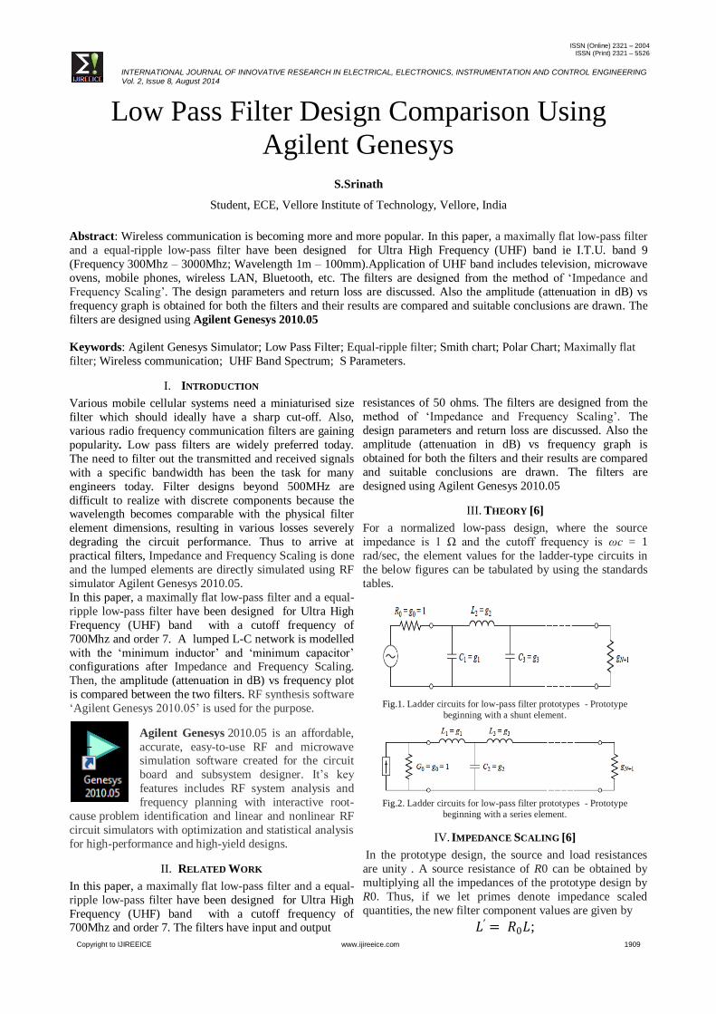
III. THEORY [6]
For a normalized low-pass design, where the source
impedance is 1 Ω and the cutoff frequency is ωc = 1
rad/sec, the element values for the ladder-type circuits in
the below figures can be tabulated by using the standards
tables.
Fig.1. Ladder circuits for low-pass filter prototypes - Prototype
beginning with a shunt element.
Fig.2. Ladder circuits for low-pass filter prototypes - Prototype
beginning with a series element.
IV. IMPEDANCE SCALING [6]
In the prototype design, the source and load resistances
are unity . A source resistance of R0 can be obtained by
multiplying all the impedances of the prototype design by
R0. Thus, if we let primes denote impedance scaled
quantities, the new filter component values are given by
𝐿′ = 𝑅0𝐿;
ISSN (Online) 2321 – 2004 ISSN (Print) 2321 – 5526
INTERNATIONAL JOURNAL OF INNOVATIVE RESEARCH IN ELECTRICAL, ELECTRONICS, INSTRUMENTATION AND CONTROL ENGINEERING Vol. 2, Issue 8, August 2014
Copyright to IJIREEICE www.ijireeice.com 1910
𝐶 ′ =𝐶
𝑅0;
𝑅′𝑆 = 𝑅0;
𝑅′𝐿 = 𝑅0𝑅𝐿; where L, C, and RL are the component values for the
original prototype.
V. FREQUENCY SCALING [6]
To change the cutoff frequency of a low-pass prototype
from unity to 𝜔𝑐 requires that we scale the frequency
dependence of the filter by the factor 1
𝜔𝑐, which is
accomplished by replacing 𝜔 by 𝜔
𝜔𝑐:
𝜔 ←𝜔
𝜔𝑐
Then the new power loss ratio will be
𝑃’𝐿𝑅 𝜔 = 𝑃𝐿𝑅 𝜔
𝜔 𝑐 ;
where ωc is the new cutoff frequency; cutoff occurs when 𝜔
𝜔𝑐= 1, or ω = ωc. This transformation can be viewed as
a stretching, or expansion, of the original passband. The
new element values are determined by applying the
substitution of 𝜔 ←𝜔
𝜔𝑐 to the series reactances, 𝑗𝜔𝐿𝑘 ,
and shunt susceptances, 𝑗𝜔𝐶𝑘 , of the prototype filter.
Thus,
𝑗 𝑋𝑘 = 𝑗(𝜔
𝜔 𝑐)𝐿𝑘 = 𝑗𝜔𝐿’𝑘 ,
𝑗 𝐵𝑘 = 𝑗 𝜔
𝜔 𝑐 𝐶𝑘 = 𝑗𝜔’𝐶𝑘 ,
which shows that the new element values are given by
𝐿′𝑘 =𝐿𝑘
𝜔𝑐
𝐶′𝑘 =𝐶𝑘
𝜔𝑐
When both impedance and frequency scaling are required,
the results of both Impedance and Frequency Scaling can
be combined to give
(1.) 𝐿’𝑘 =𝑅0𝐿𝑘
𝜔 𝑐
(2.) 𝐶’𝑘 =𝐶𝑘
𝑅0𝜔 𝑐
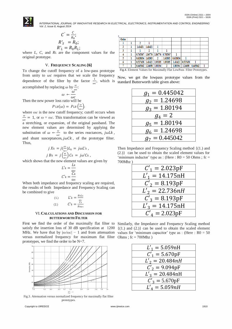
VI. CALCULATIONS AND DISCUSSION FOR
BUTTERWORTH FILTER
First we find the order of the maximally flat filter to
satisfy the insertion loss of 30 dB specification at 1200
MHz. We have that by |ω/ωc| − 1 and from attenuation
versus normalized frequency for maximum flat filter
prototypes, we find the order to be N=7.
Fig.3. Attenuation versus normalized frequency for maximally flat filter
prototypes.
Fig.4. Element Values for Maximally Flat LowPass Filter Prototypes.
Now, we get the lowpass prototype values from the
standard Butterworth table given above:
𝑔1 = 0.445042
𝑔2 = 1.24698
𝑔3 = 1.80194
𝑔4 = 2
𝑔5 = 1.80194
𝑔6 = 1.24698
𝑔7 = 0.445042
Then Impedance and Frequency Scaling method {(1.) and
(2.)} can be used to obtain the scaled element values for
„minimum inductor‟ type as : (Here : R0 = 50 Ohms ; fc =
700Mhz )
𝐶′1 = 2.023pF
𝐿′1 = 14.175nH
𝐶′2 = 8.193pF
𝐿′2 = 22.736𝑛𝐻
𝐶′3 = 8.193pF
𝐿′3 = 14.175nH
𝐶′4 = 2.023pF
Similarly, the Impedance and Frequency Scaling method
{(1.) and (2.)} can be used to obtain the scaled element values for „minimum capacitor‟ type as : (Here : R0 = 50
Ohms ; fc = 700Mhz )
𝐿′1 = 5.059nH
𝐶′1 = 5.670pF
𝐿′2 = 20.484𝑛𝐻
𝐶′2 = 9.094pF
𝐿′3 = 20.484nH
𝐶′3 = 5.670pF
𝐿′4 = 5.059𝑛𝐻
ISSN (Online) 2321 – 2004 ISSN (Print) 2321 – 5526
INTERNATIONAL JOURNAL OF INNOVATIVE RESEARCH IN ELECTRICAL, ELECTRONICS, INSTRUMENTATION AND CONTROL ENGINEERING Vol. 2, Issue 8, August 2014
Copyright to IJIREEICE www.ijireeice.com 1911
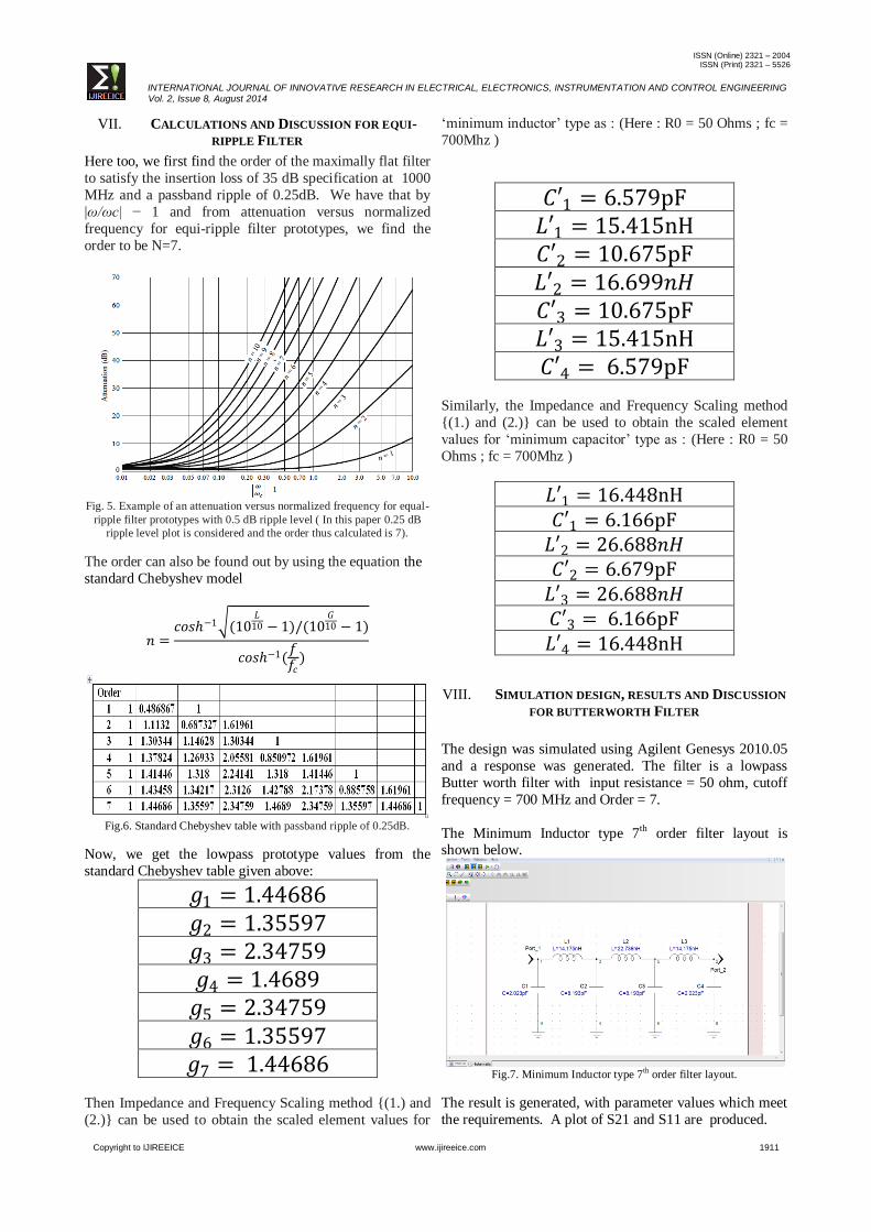
VII. CALCULATIONS AND DISCUSSION FOR EQUI-
RIPPLE FILTER
Here too, we first find the order of the maximally flat filter
to satisfy the insertion loss of 35 dB specification at 1000
MHz and a passband ripple of 0.25dB. We have that by
|ω/ωc| − 1 and from attenuation versus normalized
frequency for equi-ripple filter prototypes, we find the
order to be N=7.
Fig. 5. Example of an attenuation versus normalized frequency for equal-
ripple filter prototypes with 0.5 dB ripple level ( In this paper 0.25 dB
ripple level plot is considered and the order thus calculated is 7).
The order can also be found out by using the equation the
standard Chebyshev model
𝑛 =𝑐𝑜𝑠−1 (10
𝐿10 − 1)/(10
𝐺10 − 1)
𝑐𝑜𝑠−1(𝑓𝑓𝑐
)
Fig.6. Standard Chebyshev table with passband ripple of 0.25dB.
Now, we get the lowpass prototype values from the
standard Chebyshev table given above:
𝑔1 = 1.44686
𝑔2 = 1.35597
𝑔3 = 2.34759
𝑔4 = 1.4689
𝑔5 = 2.34759
𝑔6 = 1.35597
𝑔7 = 1.44686
Then Impedance and Frequency Scaling method {(1.) and
(2.)} can be used to obtain the scaled element values for
„minimum inductor‟ type as : (Here : R0 = 50 Ohms ; fc =
700Mhz )
𝐶′1 = 6.579pF
𝐿′1 = 15.415nH
𝐶′2 = 10.675pF
𝐿′2 = 16.699𝑛𝐻
𝐶′3 = 10.675pF
𝐿′3 = 15.415nH
𝐶′4 = 6.579pF
Similarly, the Impedance and Frequency Scaling method
{(1.) and (2.)} can be used to obtain the scaled element
values for „minimum capacitor‟ type as : (Here : R0 = 50
Ohms ; fc = 700Mhz )
𝐿′1 = 16.448nH
𝐶′1 = 6.166pF
𝐿′2 = 26.688𝑛𝐻
𝐶′2 = 6.679pF
𝐿′3 = 26.688𝑛𝐻
𝐶′3 = 6.166pF
𝐿′4 = 16.448nH
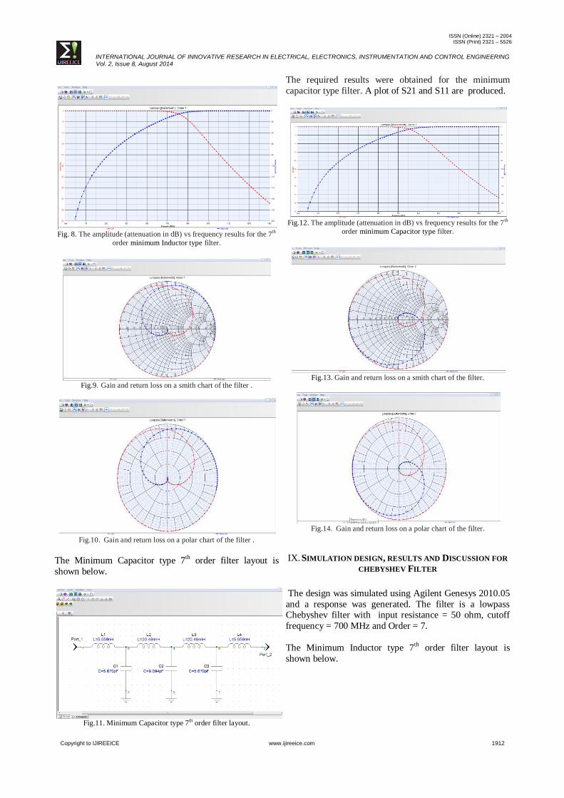
VIII. SIMULATION DESIGN, RESULTS AND DISCUSSION
FOR BUTTERWORTH FILTER
The design was simulated using Agilent Genesys 2010.05
and a response was generated. The filter is a lowpass
Butter worth filter with input resistance = 50 ohm, cutoff
frequency = 700 MHz and Order = 7.
The Minimum Inductor type 7th order filter layout is shown below.
Fig.7. Minimum Inductor type 7
th order filter layout.
The result is generated, with parameter values which meet
the requirements. A plot of S21 and S11 are produced.
ISSN (Online) 2321 – 2004 ISSN (Print) 2321 – 5526
INTERNATIONAL JOURNAL OF INNOVATIVE RESEARCH IN ELECTRICAL, ELECTRONICS, INSTRUMENTATION AND CONTROL ENGINEERING Vol. 2, Issue 8, August 2014
Copyright to IJIREEICE www.ijireeice.com 1912
Fig. 8. The amplitude (attenuation in dB) vs frequency results for the 7
th
order minimum Inductor type filter.
Fig.9. Gain and return loss on a smith chart of the filter .
Fig.10. Gain and return loss on a polar chart of the filter .
The Minimum Capacitor type 7th order filter layout is
shown below.
Fig.11. Minimum Capacitor type 7
th order filter layout.
The required results were obtained for the minimum
capacitor type filter. A plot of S21 and S11 are produced.
Fig.12. The amplitude (attenuation in dB) vs frequency results for the 7
th
order minimum Capacitor type filter.
Fig.13. Gain and return loss on a smith chart of the filter.
Fig.14. Gain and return loss on a polar chart of the filter.
IX. SIMULATION DESIGN, RESULTS AND DISCUSSION FOR
CHEBYSHEV FILTER
The design was simulated using Agilent Genesys 2010.05
and a response was generated. The filter is a lowpass Chebyshev filter with input resistance = 50 ohm, cutoff
frequency = 700 MHz and Order = 7.
The Minimum Inductor type 7th order filter layout is
shown below.
ISSN (Online) 2321 – 2004 ISSN (Print) 2321 – 5526
INTERNATIONAL JOURNAL OF INNOVATIVE RESEARCH IN ELECTRICAL, ELECTRONICS, INSTRUMENTATION AND CONTROL ENGINEERING Vol. 2, Issue 8, August 2014
Copyright to IJIREEICE www.ijireeice.com 1913
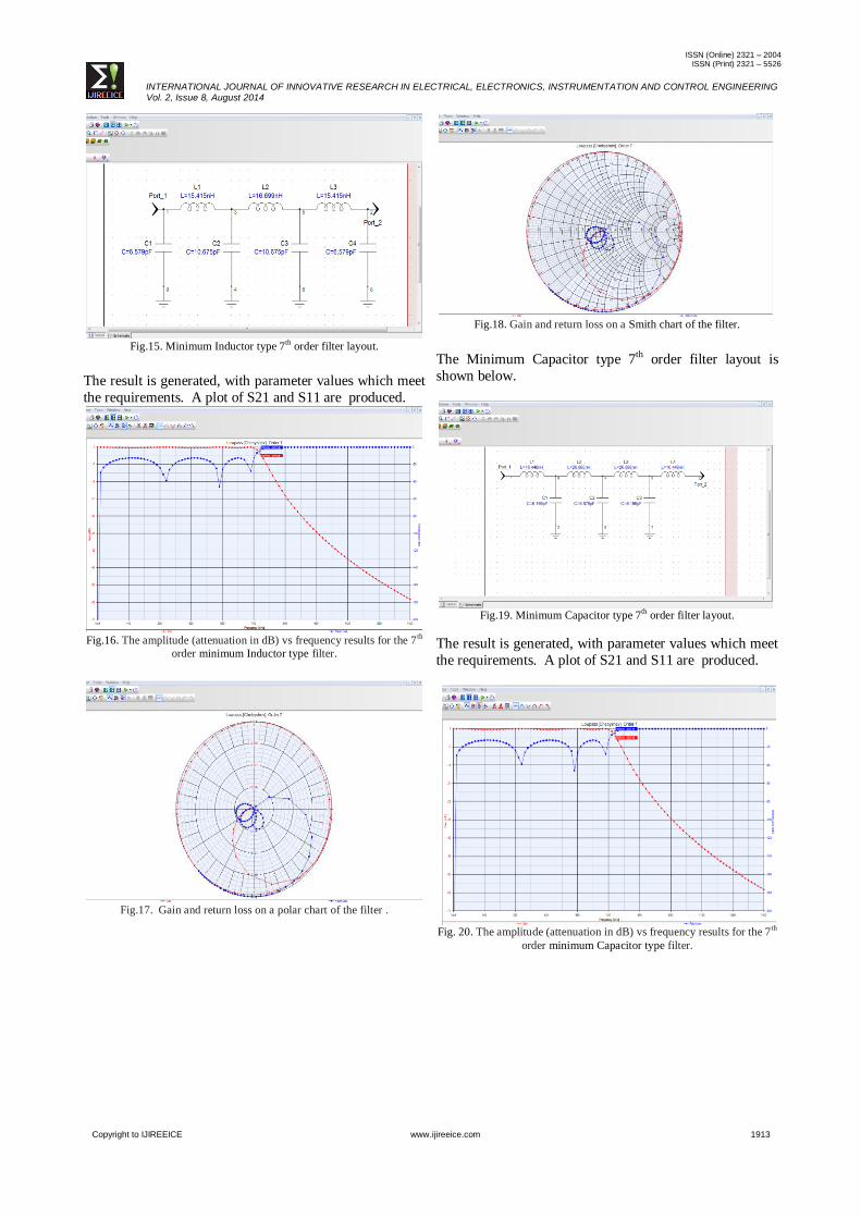
Fig.15. Minimum Inductor type 7
th order filter layout.
The result is generated, with parameter values which meet
the requirements. A plot of S21 and S11 are produced.
Fig.16. The amplitude (attenuation in dB) vs frequency results for the 7
th
order minimum Inductor type filter.
Fig.17. Gain and return loss on a polar chart of the filter .
Fig.18. Gain and return loss on a Smith chart of the filter.
The Minimum Capacitor type 7th order filter layout is
shown below.
Fig.19. Minimum Capacitor type 7
th order filter layout.
The result is generated, with parameter values which meet
the requirements. A plot of S21 and S11 are produced.
Fig. 20. The amplitude (attenuation in dB) vs frequency results for the 7
th
order minimum Capacitor type filter.
ISSN (Online) 2321 – 2004 ISSN (Print) 2321 – 5526
INTERNATIONAL JOURNAL OF INNOVATIVE RESEARCH IN ELECTRICAL, ELECTRONICS, INSTRUMENTATION AND CONTROL ENGINEERING Vol. 2, Issue 8, August 2014
Copyright to IJIREEICE www.ijireeice.com 1914
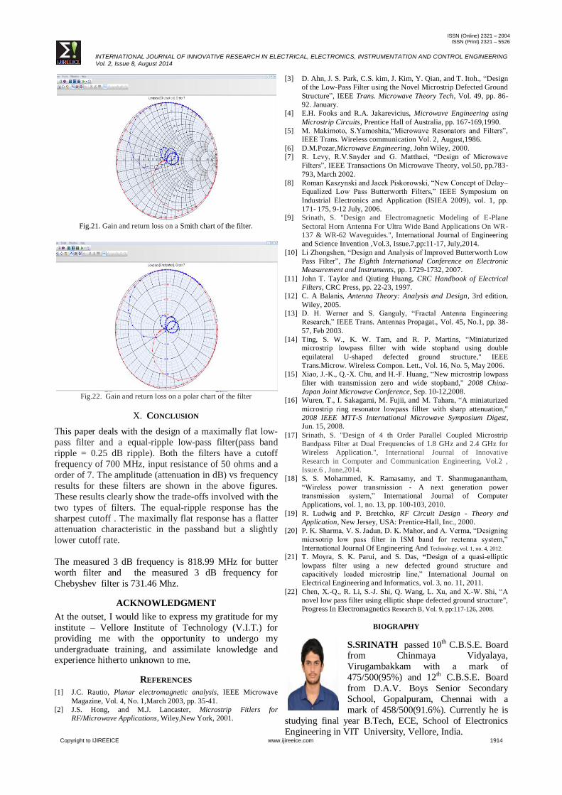
Fig.21. Gain and return loss on a Smith chart of the filter.
Fig.22. Gain and return loss on a polar chart of the filter
X. CONCLUSION
This paper deals with the design of a maximally flat low-
pass filter and a equal-ripple low-pass filter(pass band
ripple = 0.25 dB ripple). Both the filters have a cutoff
frequency of 700 MHz, input resistance of 50 ohms and a
order of 7. The amplitude (attenuation in dB) vs frequency
results for these filters are shown in the above figures.
These results clearly show the trade-offs involved with the
two types of filters. The equal-ripple response has the
sharpest cutoff . The maximally flat response has a flatter attenuation characteristic in the passband but a slightly
lower cutoff rate.
The measured 3 dB frequency is 818.99 MHz for butter
worth filter and the measured 3 dB frequency for
Chebyshev filter is 731.46 Mhz.
ACKNOWLEDGMENT
At the outset, I would like to express my gratitude for my
institute – Vellore Institute of Technology (V.I.T.) for
providing me with the opportunity to undergo my
undergraduate training, and assimilate knowledge and experience hitherto unknown to me.
REFERENCES
[1] J.C. Rautio, Planar electromagnetic analysis, IEEE Microwave
Magazine, Vol. 4, No. 1,March 2003, pp. 35-41.
[2] J.S. Hong, and M.J. Lancaster, Microstrip Fitlers for
RF/Microwave Applications, Wiley,New York, 2001.
[3] D. Ahn, J. S. Park, C.S. kim, J. Kim, Y. Qian, and T. Itoh., “Design
of the Low-Pass Filter using the Novel Microstrip Defected Ground
Structure”, IEEE Trans. Microwave Theory Tech, Vol. 49, pp. 86-
92. January.
[4] E.H. Fooks and R.A. Jakarevicius, Microwave Engineering using
Microstrip Circuits, Prentice Hall of Australia, pp. 167-169,1990.
[5] M. Makimoto, S.Yamoshita,“Microwave Resonators and Filters”,
IEEE Trans. Wireless communication Vol. 2, August,1986.
[6] D.M.Pozar,Microwave Engineering, John Wiley, 2000.
[7] R. Levy, R.V.Snyder and G. Matthaei, “Design of Microwave
Filters”, IEEE Transactions On Microwave Theory, vol.50, pp.783-
793, March 2002.
[8] Roman Kaszynski and Jacek Piskorowski, “New Concept of Delay–
Equalized Low Pass Butterworth Filters,” IEEE Symposium on
Industrial Electronics and Application (ISIEA 2009), vol. 1, pp.
171- 175, 9-12 July, 2006.
[9] Srinath, S. "Design and Electromagnetic Modeling of E-Plane
Sectoral Horn Antenna For Ultra Wide Band Applications On WR-
137 & WR-62 Waveguides.", International Journal of Engineering
and Science Invention ,Vol.3, Issue.7,pp:11-17, July,2014.
[10] Li Zhongshen, “Design and Analysis of Improved Butterworth Low
Pass Filter”, The Eighth International Conference on Electronic
Measurement and Instruments, pp. 1729-1732, 2007.
[11] John T. Taylor and Qiuting Huang, CRC Handbook of Electrical
Filters, CRC Press, pp. 22-23, 1997.
[12] C. A Balanis, Antenna Theory: Analysis and Design, 3rd edition,
Wiley, 2005.
[13] D. H. Werner and S. Ganguly, “Fractal Antenna Engineering
Research,” IEEE Trans. Antennas Propagat., Vol. 45, No.1, pp. 38-
57, Feb 2003.
[14] Ting, S. W., K. W. Tam, and R. P. Martins, “Miniaturized
microstrip lowpass fillter with wide stopband using double
equilateral U-shaped defected ground structure," IEEE
Trans.Microw. Wireless Compon. Lett., Vol. 16, No. 5, May 2006.
[15] Xiao, J.-K., Q.-X. Chu, and H.-F. Huang, “New microstrip lowpass
filter with transmission zero and wide stopband," 2008 China-
Japan Joint Microwave Conference, Sep. 10-12,2008.
[16] Wuren, T., I. Sakagami, M. Fujii, and M. Tahara, “A miniaturized
microstrip ring resonator lowpass fillter with sharp attenuation,"
2008 IEEE MTT-S International Microwave Symposium Digest,
Jun. 15, 2008.
[17] Srinath, S. "Design of 4 th Order Parallel Coupled Microstrip
Bandpass Filter at Dual Frequencies of 1.8 GHz and 2.4 GHz for
Wireless Application.", International Journal of Innovative
Research in Computer and Communication Engineering, Vol.2 ,
Issue.6 , June,2014.
[18] S. S. Mohammed, K. Ramasamy, and T. Shanmuganantham,
“Wireless power transmission - A next generation power
transmission system,” International Journal of Computer
Applications, vol. 1, no. 13, pp. 100-103, 2010.
[19] R. Ludwig and P. Bretchko, RF Circuit Design - Theory and
Application, New Jersey, USA: Prentice-Hall, Inc., 2000.
[20] P. K. Sharma, V. S. Jadun, D. K. Mahor, and A. Verma, “Designing
micrsotrip low pass filter in ISM band for rectenna system,”
International Journal Of Engineering And Technology, vol. 1, no. 4, 2012.
[21] T. Moyra, S. K. Parui, and S. Das, “Design of a quasi-elliptic
lowpass filter using a new defected ground structure and
capacitively loaded microstrip line,” International Journal on
Electrical Engineering and Informatics, vol. 3, no. 11, 2011.
[22] Chen, X.-Q., R. Li, S.-J. Shi, Q. Wang, L. Xu, and X.-W. Shi, “A
novel low pass filter using elliptic shape defected ground structure",
Progress In Electromagnetics Research B, Vol. 9, pp:117-126, 2008.
BIOGRAPHY
S.SRINATH passed 10th C.B.S.E. Board from Chinmaya Vidyalaya,
Virugambakkam with a mark of
475/500(95%) and 12th C.B.S.E. Board
from D.A.V. Boys Senior Secondary
School, Gopalpuram, Chennai with a
mark of 458/500(91.6%). Currently he is
studying final year B.Tech, ECE, School of Electronics
Engineering in VIT University, Vellore, India.