low dimension materials for extend/beyond
TRANSCRIPT
LOW DIMENSION MATERIALS FOR EXTEND/BEYOND CMOS
APPLICATIONS
by
Chin-Sheng Pang
A Dissertation
Submitted to the Faculty of Purdue University
In Partial Fulfillment of the Requirements for the degree of
Doctor of Philosophy
School of Electrical & Computer Engineering
West Lafayette, Indiana
May 2021
2
THE PURDUE UNIVERSITY GRADUATE SCHOOL
STATEMENT OF COMMITTEE APPROVAL
Dr. Zhihong Chen, Chair
School of Electrical & Computer Engineering
Dr. David B. Janes
School of Electrical & Computer Engineering
Dr. Joerg Appenzeller
School of Electrical & Computer Engineering
Dr. Peide (Peter) Ye
School of Electrical & Computer Engineering
Approved by:
Dr. Dimitrios Peroulis

3
ACKNOWLEDGMENTS
From the bottom of my heart, I would like to first appreciate my parents. Nothing can be
achieved by me without all of their supports.
I would like to appreciate my girlfriend Yu-Ching who always encourage me whenever I
felt frustrated during my PhD journey. Although we spend seven years keeping long-distance
relationship out of seven years and a half, I truly believe there is a bright future ahead of us to
explore together!
Prof. Zhihong Chen is one of the best mentors I met during my academic learning. She
spend numerous time helping me to improve my academic-relevant skills. I recall before my first
oral presentation for Device Research Conference in 2018, she discussed with me how to properly
present to different crowd of audience, and handwrote 4 pages of texts for me to prepare. She is
always open to my thoughts of research and kept encouraging me along the journey. I would like
to give her my great appreciation who makes me a well-trained PhD.
I would like to appreciate for all the fruitful discussions with prof. Joerg Appenzeller during
each of the group meeting. I enjoy the “challenging questions” he had raised, which facilitate my
PhD training and help me become well-prepared to tough questions from other researchers.
I am thankful to Prof. Peide Ye and Prof. David Janes as my committee members who
provided valuable suggestions to my research.
I would like to appreciate Prof. Sumeet Gupta who had fruitful discussions with me in my
research projects relevant to circuit implementations and demonstrations.
I am thankful to Dr. Terry Hung who gave me useful information prior to my decision of
joining the group and my moving to the West Lafayette, IN. He is also a great collaborator to work
with in some of my research projects.
I would like to appreciate Peng Wu who plays important role in my research by constantly
sharing and discussing academic-relevant materials with me. He always presented nice research
results which further facilitate my motivations to become a better PhD student.
I am thankful to Chin-Cheng Chiang, Tzu-Han Chang, and Pai-Ying Liao who spent lots
of time with me establishing a recipe for JEOL e-beam system, which proved to be extremely
important in my PhD research.

4
I appreciate all of my collaborators, Prof. Gerhard Klimeck, Prof. Robert M. Wallace, Prof.
Moon J. Kim, Shengjiao Zhang, Xiangkai Liu, Ruiping Zhou, Zheng Sun, Dr. Shu-Jen Han, Dr.
Hesameddin Ilatikhameneh, Dr. Chin-Yi Chen, Dr. Tarek Ameen, Dr. Rajib Rahman, Dr. Ava
Khosravi, Dr. Rafik Addou, Dr. Qingxiao Wang, Dr. Sergiy Krylyuk, Dr. Albert V. Davydov, Prof.
Mona E. Zaghloul, and Shiqi Guo that I am honored to work with on numerous impactful research
projects.
I am thankful to all my group members and alumni, Dr. Chun-Li Lo, Dr. Feng Zhang, Dr.
Ashish Penumatcha, Dr. Punyashloka Debashis, Dr. Vaibhav Ostwal, Suki Zhang, John Daniel,
Tingting Shen, Dr. Yuqi Zhu, Dr. Abhijith Prakash, Dr. Christopher Benjamin, Yuanqiu Tan,
Daniel Eppler, and Hao-Yu Lan who are willing to share information and have discussions with
me that are definitely helpful to my research.
I am appreciated to Yanbo He, Karam Cho, XinKang Chen, Dr. Rahul Ramamurthy, Dr.
Harsha Eragamreddy, Yen-Pu Chen, Dr. Mengwei Si and Dr. Mei-Chin Chen who had once
provided helps along my PhD journey.
The last but not least, I am extremely thankful to all the Brick staff members who maintain
an excellent environments for us to conduct our research. I would like to give my appreciation
especially to Justin Wirth and Bill Rowe who maintain the e-beam lithography systems; Dave
Lubelski, Kenny Schwartz, and Michael Bayless who work on metal evaporators; Jerry Shepard
who maintain the Fiji ALD; Neil Dilley who maintain the probe stations and help us to set up low-
temperature measurement; Dan Hosler, Richard Hosler, and Richard Harlan who work on CVD
systems and furnaces; and Joon Park who maintain the spinners and AFM.
Shout-outs to all the people who once gave me a hand during my PhD journey!
5
TABLE OF CONTENTS
LIST OF TABLES .......................................................................................................................... 8
LIST OF FIGURES ........................................................................................................................ 9
ABSTRACT .................................................................................................................................. 16
INTRODUCTION .............................................................................................. 18
1.1 Low Dimensional Materials for Extending/Beyond CMOS ............................................. 18
1.2 Structure of the Thesis ...................................................................................................... 19
MOBILITY EXTRACTION IN 2D TRANSITION METAL
DICHALCOGENIDE DEVICES – ON THE IMPORTANCE OF GATE MODULATED
CONTACT RESISTANCE .......................................................................................................... 21
2.1 Valid Methods for Mobility Extraction ............................................................................ 21
2.1.1 Hall Mobility from 4-terminal Measurement ............................................................ 21
2.1.2 Intrinsic Mobility from 4-terminal Measurement ...................................................... 21
2.1.3 Transfer Length Measurement from 2-terminal Devices .......................................... 22
2.2 Why Extraction from 2-terminal Devices is Not Suitable ................................................ 23
2.3 Overestimation of Mobility on SB Devices ...................................................................... 24
2.3.1 gm Overestimation from 2-terminal SB Devices ........................................................ 24
2.3.2 WSe2 Devices Implemented on Thin Dielectric ........................................................ 30
2.3.3 TMD-based Devices with Smaller Schottky-barrier Height ..................................... 32
2.4 Mobility and Contact Resistance vs Gate Field ................................................................ 35
2.4.1 Four-terminal Devices Implemented on 90nm SiO2 ................................................. 35
2.4.2 Four-terminal Devices Implemented on Thin Dielectric ........................................... 37
2.5 SiNx N-doping on WSe2 Devices Implemented on 90nm SiO2 ........................................ 39
2.6 Appendix ........................................................................................................................... 41
2.6.1 Convoluted gm with RC and RCH Dependence ........................................................... 41
2.6.2 Worst Case of Mobility Extraction ............................................................................ 41
2.7 Conclusion ........................................................................................................................ 42
DOPING STRATEGIES ON 2D WSE2 ............................................................. 43
3.1 Dealing with a Huge RC .................................................................................................... 43
3.2 SiNx N-doping .................................................................................................................. 45
6
3.3 O2-plasma P-doping .......................................................................................................... 47
3.3.1 Temperature-dependent Tunable Doping Scheme .................................................... 47
3.3.2 Direct Observations of Schottky-Barrier Realignment.............................................. 58
3.4 Nitric Oxide P-doping ....................................................................................................... 61
3.5 Appendix ........................................................................................................................... 64
3.6 Conclusion ........................................................................................................................ 65
ULTRA-SCALED DIELECTRIC FOR HIGH PERFORMANCE WS2-FETS . 66
4.1 Low Dimensional Materials as Promising Candidates for Logic Devices ....................... 66
4.2 Multilayer WS2 FETs ........................................................................................................ 67
4.2.1 Ultra-scale Dielectric WS2-FETs ............................................................................... 67
4.2.2 Off-state Behavior ..................................................................................................... 69
4.2.3 On-state Performance ................................................................................................ 73
4.3 Monolayer WS2 FETs ....................................................................................................... 80
4.3.1 Ultra-scale Dielectric WS2-FETs ............................................................................... 80
4.3.2 Off-state Behavior ..................................................................................................... 81
4.3.3 On-state Performance ................................................................................................ 84
4.4 Benchmarking ................................................................................................................... 87
4.4.1 Off-state Behavior ..................................................................................................... 87
4.4.2 On-state Performance ................................................................................................ 89
4.5 Conclusion ........................................................................................................................ 92
RECONFIGURABLE DEVICES – FOR MOSFET, TFET AND DIODE
OPERATION ........................................................................................................................... 93
5.1 Electrostatically Reconfigurable Devices ......................................................................... 93
5.2 Choice of Channel Materials in Our Study ....................................................................... 95
5.3 Device Implementation ..................................................................................................... 95
5.4 MOSFET/TFET Operation ............................................................................................... 99
5.4.1 MOSFET Operation (Thermionic Emission) ............................................................ 99
5.4.2 TFET Operation (Band-to-band Tunneling) ............................................................ 100
5.4.3 Atomistic Quantum Transport Simulation ............................................................... 104
5.4.4 Optimizing Channel Thicknesses ............................................................................ 106
5.5 Diode Operation .............................................................................................................. 107
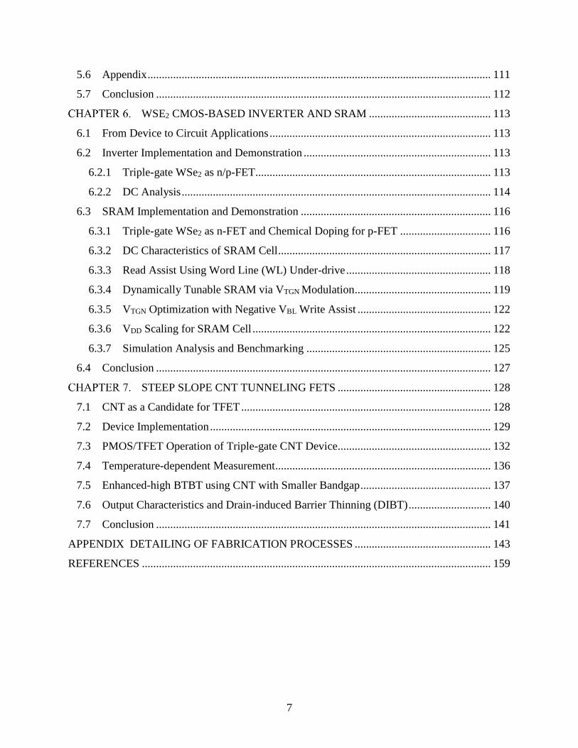
7
5.6 Appendix ......................................................................................................................... 111
5.7 Conclusion ...................................................................................................................... 112
WSE2 CMOS-BASED INVERTER AND SRAM ........................................... 113
6.1 From Device to Circuit Applications .............................................................................. 113
6.2 Inverter Implementation and Demonstration .................................................................. 113
6.2.1 Triple-gate WSe2 as n/p-FET ................................................................................... 113
6.2.2 DC Analysis ............................................................................................................. 114
6.3 SRAM Implementation and Demonstration ................................................................... 116
6.3.1 Triple-gate WSe2 as n-FET and Chemical Doping for p-FET ................................ 116
6.3.2 DC Characteristics of SRAM Cell ........................................................................... 117
6.3.3 Read Assist Using Word Line (WL) Under-drive ................................................... 118
6.3.4 Dynamically Tunable SRAM via VTGN Modulation ................................................ 119
6.3.5 VTGN Optimization with Negative VBL Write Assist ............................................... 122
6.3.6 VDD Scaling for SRAM Cell .................................................................................... 122
6.3.7 Simulation Analysis and Benchmarking ................................................................. 125
6.4 Conclusion ...................................................................................................................... 127
STEEP SLOPE CNT TUNNELING FETS ...................................................... 128
7.1 CNT as a Candidate for TFET ........................................................................................ 128
7.2 Device Implementation ................................................................................................... 129
7.3 PMOS/TFET Operation of Triple-gate CNT Device...................................................... 132
7.4 Temperature-dependent Measurement ............................................................................ 136
7.5 Enhanced-high BTBT using CNT with Smaller Bandgap .............................................. 137
7.6 Output Characteristics and Drain-induced Barrier Thinning (DIBT) ............................. 140
7.7 Conclusion ...................................................................................................................... 141
APPENDIX DETAILING OF FABRICATION PROCESSES ................................................ 143
REFERENCES ........................................................................................................................... 159

8
LIST OF TABLES
Table 4.1 Off-State Behaviors Comparison © [2021] IEEE ....................................................... 88
Table 6.1 Performance comparison of WSe2 SRAM to other flexible electronics technologies ©
[2018] IEEE ................................................................................................................................ 126
9
LIST OF FIGURES
Figure 2.1 (a) A schematic illustration and (b) scanning electron microscope (SEM) image of a 4-
terminal device structure, where LG is the channel length, dL is the distance between two voltage
probes V1 and V2, and Wprobe is the width of each voltage probe. ................................................ 22
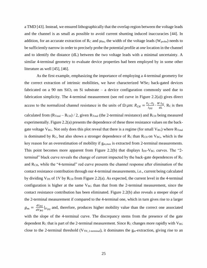
Figure 2.2 (a) 4-terminal (channel) and 2-terminal (total) as well as contact resistance as a function
of back-gate voltage. (b) Comparison of 2- and 4-terminal IDS-VBG measurements on the same
WSe2 FET, where distinct differences in slope and threshold voltage of the IDS-VBG curves are
observed. (c) Comparison of 2-terminal and 4-terminal transconductance extracted from Figure
2.2(b). (d) Comparison of the channel mobility values as a function of overdrive voltage for
different extraction methods. (e) Band diagrams of the WSe2 FET at the two threshold voltages.
(f) Log(RCH) vs log(VOV) with different VTH being used. (g) Log(RCH) vs. log(VBG-VTH_2-terminal)
for MoSe2-FETs, showing a slope that is smaller than “-1” for all devices irrespective of TCH. (h)
2-terminal and 4-terminal VTH for 8 different WSe2 devices on 90nm SiO2. ............................... 28
Figure 2.3 (a) Transfer and (b) output characteristics of a WSe2 FET implemented on a thin gate
dielectric. (c) Resistance values modulated by back-gated scheme on thin gate dielectric. (d)
Comparison of 2- and 4-terminal linear IDS-VBG for a WSe2 FET implemented on a thin gate
dielectric. Note that the slopes of the IDS-VBG curves and VTH extraction are similar (different
from Figure 2.2(b)). (e) Comparison of 2-terminal and 4-terminal transconductance extracted from
Figure 2.2(d). (f) Comparison of channel mobility values as a function of overdrive voltage with
different extraction methods. Note that the thin gate dielectric alleviates the contact resistance
contribution impact in 2-terminal measurements. ........................................................................ 31
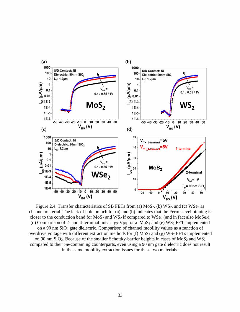
Figure 2.4 Transfer characteristics of SB FETs from (a) MoS2, (b) WS2, and (c) WSe2 as channel
material. The lack of hole branch for (a) and (b) indicates that the Fermi-level pinning is closer to
the conduction band for MoS2 and WS2 if compared to WSe2 (and in fact also MoSe2). (d)
Comparison of 2- and 4-terminal linear IDS-VBG for a MoS2 and (e) WS2 FET implemented on a
90 nm SiO2 gate dielectric. Comparison of channel mobility values as a function of overdrive
voltage with different extraction methods for (f) MoS2 and (g) WS2 FETs implemented on 90 nm
SiO2. Because of the smaller Schottky-barrier heights in cases of MoS2 and WS2 compared to their
Se-containing counterparts, even using a 90 nm gate dielectric does not result in the same mobility
extraction issues for these two materials. ..................................................................................... 33
Figure 2.5 Intrinsic mobility as a function of gate field extracted from 4-terminal devices for (a)
WSe2, (b) MoS2, and (c) WS2 with different channel thicknesses................................................ 36
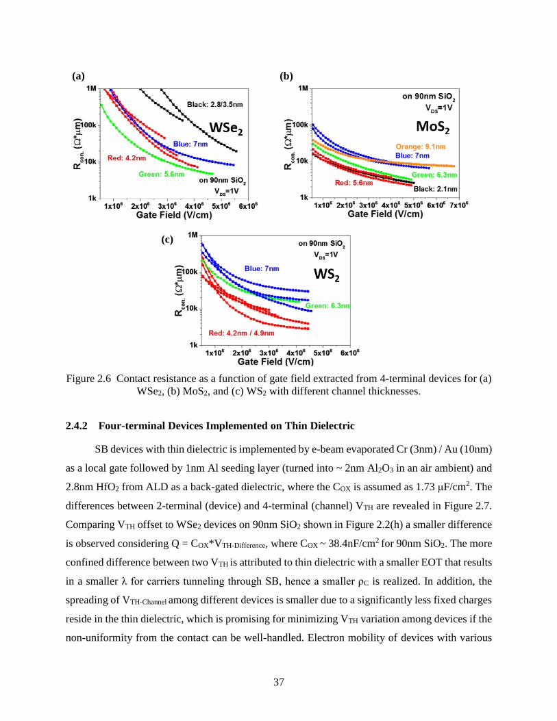
Figure 2.6 Contact resistance as a function of gate field extracted from 4-terminal devices for (a)
WSe2, (b) MoS2, and (c) WS2 with different channel thicknesses................................................ 37
Figure 2.7 2-terminal (device) and 4-terminal (channel) VTH for 7 different devices based on 4-
terminal WSe2 devices with thin dielectric. .................................................................................. 38
Figure 2.8 Intrinsic mobility as a function of gate field extracted from 4-terminal devices for (a)
WSe2 and (b) MoS2 with different channel thicknesses on thin dielectric. .................................. 38
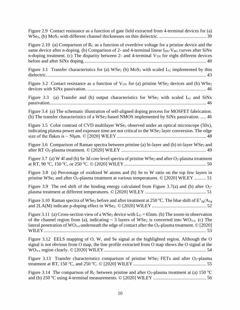
10
Figure 2.9 Contact resistance as a function of gate field extracted from 4-terminal devices for (a)
WSe2, (b) MoS2 with different channel thicknesses on thin dielectric. ........................................ 39
Figure 2.10 (a) Comparison of RC as a function of overdrive voltage for a pristine device and the
same device after n-doping. (b) Comparison of 2- and 4-terminal linear IDS-VBG curves after SiNx
n-doping treatment. (c) The disparity between 2- and 4-terminal VTH for eight different devices
before and after SiNx doping. ....................................................................................................... 40
Figure 3.1 Transfer characteristics for (a) WSe2 (b) MoS2 with scaled LG implemented by thin
dielectric. ....................................................................................................................................... 43
Figure 3.2 Contact resistance as a function of VOV for (a) pristine WSe2 devices and (b) WSe2
devices with SiNx passivation. ..................................................................................................... 46
Figure 3.3 (a) Transfer and (b) output characteristics for WSe2 with scaled LG and SiNx
passivation..................................................................................................................................... 46
Figure 3.4 (a) The schematic illustration of self-aligned doping process for MOSFET fabrication.
(b) The transfer characteristics of a WSe2-based NMOS implemented by SiNx passivation. ..... 46
Figure 3.5 Color contrast of CVD multilayer WSe2 observed under an optical microscope (50x),
indicating plasma power and exposure time are not critical to the WSe2 layer conversion. The edge
size of the flakes is ~ 50μm. © [2020] WILEY ............................................................................ 48
Figure 3.6 Comparison of Raman spectra between pristine (a) bi-layer and (b) tri-layer WSe2 and
after RT O2-plasma treatment. © [2020] WILEY ........................................................................ 49
Figure 3.7 (a) W 4f and (b) Se 3d core level spectra of pristine WSe2 and after O2-plasma treatment
at RT, 90 oC, 150 oC, or 250 oC. © [2020] WILEY ...................................................................... 50
Figure 3.8 (a) Percentage of oxidized W atoms and (b) Se to W ratio on the top few layers in
pristine WSe2 and after O2-plasma treatment at various temperatures. © [2020] WILEY .......... 51
Figure 3.9 The red shift of the binding energy calculated from Figure 3.7(a) and (b) after O2-
plasma treatment at different temperatures. © [2020] WILEY .................................................... 51
Figure 3.10 Raman spectra of WSe2 before and after treatment at 250 oC. The blue shift of E12g/A1g
and 2LA(M) indicate p-doping effect in WSe2. © [2020] WILEY .............................................. 52
Figure 3.11 (a) Cross-section view of a WSe2 device with LG = 65nm. (b) The zoom-in observation
of the channel region from (a), indicating ~ 3 layers of WSe2 is converted into WO3-x. (c) The
lateral penetration of WO3-x underneath the edge of contact after the O2-plasma treatment. © [2020]
WILEY .......................................................................................................................................... 53
Figure 3.12 EELS mapping of O, W, and Se signal at the highlighted region. Although the O
signal is not obvious from O map, the line profile extracted from O map shows the O signal at the
WO3-x region clearly. © [2020] WILEY ....................................................................................... 54
Figure 3.13 Transfer characteristics comparison of pristine WSe2 FETs and after O2-plasma
treatment at RT, 150 oC, and 250 oC. © [2020] WILEY .............................................................. 55
Figure 3.14 The comparison of RC between pristine and after O2-plasma treatment at (a) 150 oC
and (b) 250 oC using 4-terminal measurements. © [2020] WILEY ............................................. 56
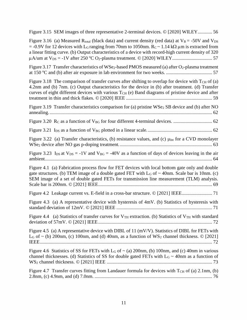
11
Figure 3.15 SEM images of three representative 2-terminal devices. © [2020] WILEY............ 56
Figure 3.16 (a) Measured Rtotal (black data) and current density (red data) at VB = -50V and VDS
= -0.9V for 12 devices with LG ranging from 70nm to 1050nm. RC ~ 1.14 k m is extracted from
a linear fitting curve. (b) Output characteristics of a device with record-high current density of 320
A/um at VDS = -1V after 250 oC O2-plasma treatment. © [2020] WILEY................................. 57
Figure 3.17 Transfer characteristics of WSe2-based PMOS measured (a) after O2-plasma treatment
at 150 oC and (b) after air exposure in lab environment for two weeks. ...................................... 57
Figure 3.18 The comparison of transfer curves after shifting to overlap for device with TCH of (a)
4.2nm and (b) 7nm. (c) Output characteristics for the device in (b) after treatment. (d) Transfer
curves of eight different devices with various TCH (e) Band diagrams of pristine device and after
treatment in thin and thick flakes. © [2020] IEEE ....................................................................... 59
Figure 3.19 Transfer characteristics comparison for (a) pristine WSe2 SB device and (b) after NO
annealing. ...................................................................................................................................... 62
Figure 3.20 RC as a function of VBG for four different 4-terminal devices. ................................ 62
Figure 3.21 IDS as a function of VBG plotted in a linear scale. ..................................................... 62
Figure 3.22 (a) Transfer characteristics, (b) resistance values, and (c) μInt for a CVD monolayer
WSe2 device after NO gas p-doping treatment. ............................................................................ 63
Figure 3.23 IDS at VDS = -1V and VBG = -40V as a function of days of devices leaving in the air
ambient. ......................................................................................................................................... 64
Figure 4.1 (a) Fabrication process flow for FET devices with local bottom gate only and double
gate structures. (b) TEM image of a double gated FET with LG of ~ 40nm. Scale bar is 10nm. (c)
SEM image of a set of double gated FETs for transmission line measurement (TLM) analysis.
Scale bar is 200nm. © [2021] IEEE .............................................................................................. 69
Figure 4.2 Leakage current vs. E-field in a cross-bar structure. © [2021] IEEE ......................... 71
Figure 4.3 (a) A representative device with hysteresis of 4mV. (b) Statistics of hysteresis with
standard deviation of 12mV. © [2021] IEEE ............................................................................... 71
Figure 4.4 (a) Statistics of transfer curves for VTH extraction. (b) Statistics of VTH with standard
deviation of 57mV. © [2021] IEEE .............................................................................................. 72
Figure 4.5 (a) A representative device with DIBL of 11 (mV/V). Statistics of DIBL for FETs with
LG of ~ (b) 200nm, (c) 100nm, and (d) 40nm, as a function of WS2 channel thickness. © [2021]
IEEE .............................................................................................................................................. 72
Figure 4.6 Statistics of SS for FETs with LG of ~ (a) 200nm, (b) 100nm, and (c) 40nm in various
channel thicknesses. (d) Statistics of SS for double gated FETs with LG ~ 40nm as a function of
WS2 channel thickness. © [2021] IEEE ....................................................................................... 73
Figure 4.7 Transfer curves fitting from Landauer formula for devices with TCH of (a) 2.1nm, (b)
2.8nm, (c) 4.9nm, and (d) 7.0nm. ................................................................................................. 76
12
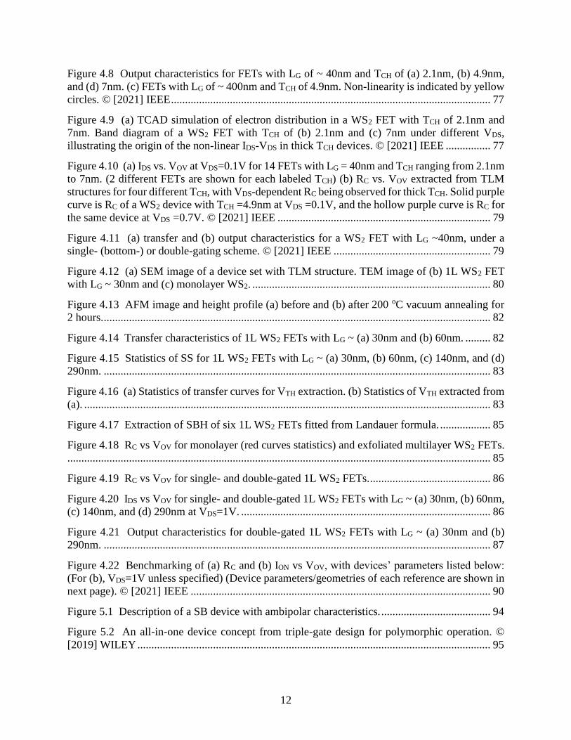
Figure 4.8 Output characteristics for FETs with LG of ~ 40nm and TCH of (a) 2.1nm, (b) 4.9nm,
and (d) 7nm. (c) FETs with LG of ~ 400nm and TCH of 4.9nm. Non-linearity is indicated by yellow
circles. © [2021] IEEE .................................................................................................................. 77
Figure 4.9 (a) TCAD simulation of electron distribution in a WS2 FET with TCH of 2.1nm and
7nm. Band diagram of a WS2 FET with TCH of (b) 2.1nm and (c) 7nm under different VDS,
illustrating the origin of the non-linear IDS-VDS in thick TCH devices. © [2021] IEEE ................ 77
Figure 4.10 (a) IDS vs. VOV at VDS=0.1V for 14 FETs with LG = 40nm and TCH ranging from 2.1nm
to 7nm. (2 different FETs are shown for each labeled TCH) (b) RC vs. VOV extracted from TLM
structures for four different TCH, with VDS-dependent RC being observed for thick TCH. Solid purple
curve is RC of a WS2 device with TCH =4.9nm at VDS =0.1V, and the hollow purple curve is RC for
the same device at VDS =0.7V. © [2021] IEEE ............................................................................ 79
Figure 4.11 (a) transfer and (b) output characteristics for a WS2 FET with LG ~40nm, under a
single- (bottom-) or double-gating scheme. © [2021] IEEE ........................................................ 79
Figure 4.12 (a) SEM image of a device set with TLM structure. TEM image of (b) 1L WS2 FET
with LG ~ 30nm and (c) monolayer WS2. ..................................................................................... 80
Figure 4.13 AFM image and height profile (a) before and (b) after 200 oC vacuum annealing for
2 hours. .......................................................................................................................................... 82
Figure 4.14 Transfer characteristics of 1L WS2 FETs with LG ~ (a) 30nm and (b) 60nm. ......... 82
Figure 4.15 Statistics of SS for 1L WS2 FETs with LG ~ (a) 30nm, (b) 60nm, (c) 140nm, and (d)
290nm. .......................................................................................................................................... 83
Figure 4.16 (a) Statistics of transfer curves for VTH extraction. (b) Statistics of VTH extracted from
(a). ................................................................................................................................................. 83
Figure 4.17 Extraction of SBH of six 1L WS2 FETs fitted from Landauer formula. .................. 85
Figure 4.18 RC vs VOV for monolayer (red curves statistics) and exfoliated multilayer WS2 FETs.
....................................................................................................................................................... 85
Figure 4.19 RC vs VOV for single- and double-gated 1L WS2 FETs. ........................................... 86
Figure 4.20 IDS vs VOV for single- and double-gated 1L WS2 FETs with LG ~ (a) 30nm, (b) 60nm,
(c) 140nm, and (d) 290nm at VDS=1V. ......................................................................................... 86
Figure 4.21 Output characteristics for double-gated 1L WS2 FETs with LG ~ (a) 30nm and (b)
290nm. .......................................................................................................................................... 87
Figure 4.22 Benchmarking of (a) RC and (b) ION vs VOV, with devices’ parameters listed below:
(For (b), VDS=1V unless specified) (Device parameters/geometries of each reference are shown in
next page). © [2021] IEEE ........................................................................................................... 90
Figure 5.1 Description of a SB device with ambipolar characteristics. ....................................... 94
Figure 5.2 An all-in-one device concept from triple-gate design for polymorphic operation. ©
[2019] WILEY .............................................................................................................................. 95
13
Figure 5.3 (a) to (d) Illustrations of device fabrication processes. (e) A colored SEM image of the
WSe2 triple-gate device. © [2019] WILEY .................................................................................. 97
Figure 5.4 (a) Photoluminescence spectrum and (b) Raman spectrum for monolayer CVD WSe2.
© [2019] WILEY .......................................................................................................................... 98
Figure 5.5 (a) AFM image and (b) height profile following the white dash line in (a). © [2019]
WILEY .......................................................................................................................................... 98
Figure 5.6 (a) Transfer characteristics at different VTGS, corresponding to MOSFET operation in
case I and TFET operation in case III, respectively. (b) - (d) Qualitative band diagrams of the
triple-gate device with different voltage bias configurations. © [2019] WILEY ....................... 102
Figure 5.7 n-type MOSFET operation biased at positive VTGD and VTGS. ................................ 103
Figure 5.8 Output characteristics for an n-MOSFET and a p-MOSFET. © [2019] WILEY .... 103
Figure 5.9 Transfer characteristics of a multi-layer WSe2 device at (a) positive VTGD = +2.5V for
n-type MOSFET to TFET transition and (b) negative VTGD = -2.5V for p-type MOSFET to TFET
transition. © [2019] WILEY ....................................................................................................... 104
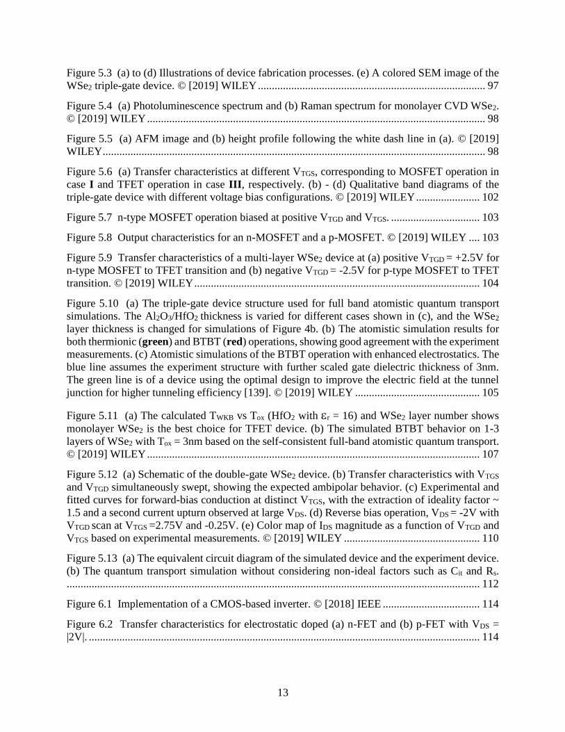
Figure 5.10 (a) The triple-gate device structure used for full band atomistic quantum transport
simulations. The Al2O3/HfO2 thickness is varied for different cases shown in (c), and the WSe2
layer thickness is changed for simulations of Figure 4b. (b) The atomistic simulation results for
both thermionic (green) and BTBT (red) operations, showing good agreement with the experiment
measurements. (c) Atomistic simulations of the BTBT operation with enhanced electrostatics. The
blue line assumes the experiment structure with further scaled gate dielectric thickness of 3nm.
The green line is of a device using the optimal design to improve the electric field at the tunnel
junction for higher tunneling efficiency [139]. © [2019] WILEY ............................................. 105
Figure 5.11 (a) The calculated TWKB vs Tox (HfO2 with r = 16) and WSe2 layer number shows
monolayer WSe2 is the best choice for TFET device. (b) The simulated BTBT behavior on 1-3
layers of WSe2 with Tox = 3nm based on the self-consistent full-band atomistic quantum transport.
© [2019] WILEY ........................................................................................................................ 107
Figure 5.12 (a) Schematic of the double-gate WSe2 device. (b) Transfer characteristics with VTGS
and VTGD simultaneously swept, showing the expected ambipolar behavior. (c) Experimental and
fitted curves for forward-bias conduction at distinct VTGS, with the extraction of ideality factor ~
1.5 and a second current upturn observed at large VDS. (d) Reverse bias operation, VDS = -2V with
VTGD scan at VTGS =2.75V and -0.25V. (e) Color map of IDS magnitude as a function of VTGD and
VTGS based on experimental measurements. © [2019] WILEY ................................................. 110
Figure 5.13 (a) The equivalent circuit diagram of the simulated device and the experiment device.
(b) The quantum transport simulation without considering non-ideal factors such as Cit and Rs.
..................................................................................................................................................... 112
Figure 6.1 Implementation of a CMOS-based inverter. © [2018] IEEE ................................... 114
Figure 6.2 Transfer characteristics for electrostatic doped (a) n-FET and (b) p-FET with VDS =
|2V|. ............................................................................................................................................. 114
14
Figure 6.3 (a) Voltage transfer curves of WSe2 CMOS logic inverter and (b) corresponding NML,
NMH, and NM/VDD extracted using piecewise linear approximation. © [2018] IEEE .............. 115
Figure 6.4 Voltage transfer curves of a WSe2 CMOS inverter with VDD supply from 2 to 3V. The
corresponding butterfly curves are presented as dotted lines. The inset shows the voltage gains for
various VDD. © [2018] IEEE ....................................................................................................... 115
Figure 6.5 (a) Illustration of p-FET with exposed extended S/D regions for O2-plasma treatment.
Transfer characteristics of (b) a pristine device with VBG-dependent current injection and (c) a p-
FET after O2-plasma treatment with VBG being floating. © [2018] IEEE .................................. 117
Figure 6.6 (a) SRAM cell design wit VDD connected to VTGN. (b) VTCs of two different device
sets. (c) NM extraction of hold and read from butterfly curves, and from write curves. The
individual NM values indicate a write-favored SRAM behavior. © [2018] IEEE ..................... 118
Figure 6.7 (a) Measured butterfly curves (considering symmetric SRAM) with WL under-drive
technique. (b) NM for R/W with respect to different VWL showing a significant enhancement in
read stability with read SNM = 0.39V at VWL = 0.8V. © [2018] IEEE...................................... 119
Figure 6.8 (a) SRAM cell design with VDD connected to VBL for hold operation and (b) an optical
image of the experimental device set. (c) VTCs and inset shows dynamically tunable NMs
extracted from butterfly curves, resulted from different doping strength of the n-FET by tuning
VTGN. © [2018] IEEE .................................................................................................................. 120
Figure 6.9 (a) SRAM cell design with VDD connected to VWL. VTCs with various VTGN at (b)
VBL=1.5V and (c) VBL=0V. (d) The square fitting for R/W NM evaluation at VTGN=1, 1.25, and
1.5V. (e) NM of R/W with respect to various VTNG. © [2018] IEEE ......................................... 121
Figure 6.10 (a) VTCs comparison with the negative VBL technique. (b) R/W NM with an enhanced
write stability along with the VTGN tunability. © [2018] IEEE .................................................. 122
Figure 6.11 Measured butterfly curves for (a) read and (b) write operation at different VDD. (c)
NM of R/W with respect to different VDD shows voltage scaling up to 1.2V. © [2018] IEEE .. 123
Figure 6.12 Measured butterfly curves with the GND lowering technique at different biased
voltages. © [2018] IEEE ............................................................................................................. 124
Figure 6.13 R/W NM with the negative VBL and GND lowering technique at various VDD shows
enhanced R/W stability for SRAM to operate at scaled VDD = 0.8V. © [2018] IEEE ............... 124
Figure 6.14 The model used to simulate WSe2-based SRAM transient behavior. © [2018] IEEE
..................................................................................................................................................... 125
Figure 6.15 Projected read/write time and power at different VDD from simulations calibrated to
experiments. © [2018] IEEE ....................................................................................................... 126
Figure 7.1 (a) Schematic illustration of a CNT triple-gate device. (b) SEM image of an as-
fabricated CNT triple-gate device. .............................................................................................. 130
Figure 7.2 (a) CNTs were transferred onto Si/SiO2 substrate and was identified rapidly by SEM.
(b) Pd was deposited 30nm by e-beam evaporator as S/D contact electrodes. (c) 6nm HfO2 was
deposited by ALD at 95oC followed by (d1) 30nm Ni deposited as VTGS/D electrodes, by using
15
PMMA lift-off process. (d2) SEM image after (d1) step. (e) The same ALD followed by (f1) the
same Ni deposition as VTG electrode was carried out by PMMA lift-off process. (f2) SEM image
of the as-fabricated tri-gate device. ............................................................................................. 131
Figure 7.3 (a) Transfer characteristics as a function of VTG at VDS = -0.5V, VTGD = -2V, and VTGS
varying from -1.25V to +3V. (b) Schematic band diagrams for varying VTGS at negative VTG and
VTGD. ........................................................................................................................................... 134
Figure 7.4 (a) Schematic illustration and (b) SEM image of the as-fabricated device with two local
bottom gates and one top gate. (c) Transfer characteristics for VTG sweeping from -2V to 2V as a
primary scan with VBGS varying from -2V to 3V. The SS.BTBT > 60mV/dec is revealed. .......... 135
Figure 7.5 (a) Transfer characteristics measured at T=150K, 200K and 295K. ITG is the TG leakage
current. (b) Cumulative data of SS extracted for thermionic emission (VTGS = -2V) and BTBT
(VTGS = 3V) operation. ................................................................................................................ 137
Figure 7.6 (a) Transmission probability as functions of EOT and Eg, with a set of equal probability
lines marked. Relative dielectric constant of ntε = 2 and tunneling window ΔΦ= 0.5eV are used
for the contour plot. Red solid stars are devices fabricated with the same EOT = 1.5nm but CNTs
with Eg = 1.4eV and 0.65eV, showing an increasing transmission probability of TWKB ~ 0.36 to
0.50 with decreasing bandgap. The red hollow star is a projection of TWKB ~ 0.66, using CNT with
Eg = 0.65eV and dielectric with EOT =0.5nm. (b) Transfer characteristics as a function of VTG at
VDS = -0.5V, VTGD = -2V and VTGS varying from -1.5V to +3V. (c) Cumulative data of SS extracted
for thermionic emission (VTGS = -1.5V) and BTBT (VTGS = 3V), both at VDS = -0.5V and VTGD =
-2V. ............................................................................................................................................. 139
Figure 7.7 (a) AFM image and (b) height profile of CNT used in the triple-gate device shown in
Figure 7.3(a). ............................................................................................................................... 140
Figure 7.8 (a) Characteristics for the PMOS operation with linear I-V at the low VDS regime. (b)
Characteristics for the TFET operation with non-linear features at low VDS, mainly due to the drain
induced barrier thinning effect. ................................................................................................... 141
16
ABSTRACT
2-dimensional layered materials, transition metal dichalcogenides (TMDs) are considered
promising candidates for the post-Si era. They have attracted wide attention from both fundamental
and applied research communities, owing to their unique material properties and potential
applications including logic and memory devices. The key reason that TMD materials are excellent
channel material choices for logic devices is that their inherent layered-structures allowing uniform
thickness control with atomic-level precision and can reach the ultimate monolayer thickness limit
of ~ 0.7nm, which is desirable for the implementation of ultra-scaled devices to maintain excellent
electrostatic control.
In this thesis, I will first focus on a unique contact gating on TMD-based Schottky-barrier
transistors and discuss in great detail the impacts of current injection from source/drain contacts
to channel regions in a typical back-gated structure. I will reveal a commonly observed
overestimation of TMD mobility when substantially large contact resistance has a strong gate
dependence, and suggest that an appropriate method is necessary for precise mobility extraction.
For extending CMOS beyond Si, various extrinsic doping schemes are investigated to achieve a
much-reduced contact resistance (RC) on tungsten diselenide (WSe2) which is associated with the
Schottky-barrier height. Devices implemented on ultra-thin gate dielectric are then explored on
tungsten disulfide (WS2) with various TMD body thicknesses (TCH), with an excellent off-state
behavior and on-state performance being achieved on properly selected TCH based on our statistics.
The observed ultra-low RC and record-high on-state current at a much-scaled overdrive (VOV)
highlights the advantages and necessities of exploiting ultra-thin gate dielectric on TMD-based
electronics.
The second part of the thesis focuses on beyond CMOS applications including
reconfigurable logics and tunneling field-effect transistors (TFET). Owing to ultra-thin TCH in low
dimensional materials, the triple-gate design allows efficient electrostatic control on WSe2 and
carbon nanotube (CNT) by creating various doping types and concentrations within different
channel segments. Therefore, a single triple-gate device can operate as a metal oxide
semiconductor field-effect transistor (MOSFET), a TFET, or a diode depending on the choice of
the gate biases. In the TFET mode, a steep subthreshold slope less than 60 mV/dec has been
achieved in the CNT devices at room temperature. To extend the applications from device to

17
circuits, the capability of modulating the device on-state performance is utilized in a WSe2 CMOS-
based inverter and static random access memory (SRAM) design to improve the read and write
stability and achieve a low voltage operation.
18
INTRODUCTION
1.1 Low Dimensional Materials for Extending/Beyond CMOS
The advent of complementary metal–oxide–semiconductor (CMOS) technology following
the Gordon Moore’s law [1] for the last few decades has changed our society dramatically. Silicon
as the main character has sustained demands of extreme device scaling for high integration density
and high speed to fulfill multiple functionalities of electronics with tolerant power consumption.
It is currently approaching the 5nm technology node at the year of 2021 [2]. Nevertheless, it is
foreseen that Si transistors would rapidly approach the scaled channel length limit due to the short
channel effect (SCE) of direct source-to-drain tunneling, thus leading to severe drain-induce
barrier lowering (DIBL) and subthreshold slope (SS) degradation, ending up with substantial off-
state leakage and unbearable power consumption.
Transition metal dichalcogenide (TMD) as layered 2D materials are of utmost potential
candidates to extend CMOS technology which have been received significant attention. Extensive
applications have been demonstrated in recent studies including logic-, opto-, flexible-, bio-/gas-
sensing, spin-, neuromorphic-, and memory-devices/electronics [3]–[15]. The reasons that make
these materials attractive are their semiconducting-behavior, a reasonable carrier effective mass
and bandgap, and particularly, their ultra-thin channel thickness (TCH ~ 0.7nm for 2D TMD
materials in monolayer form) that allows excellent gate control for ultra-scaled devices.
Importantly, an excellent electronic transport property is maintained even at such scaled channel
thickness compared to a severe mobility roll-off in Si material [16]–[18]. In addition, a lack of
dangling bonds provide a clean surface for dielectric implementation with a negligible interface
trap density theoretically to facilitate desired device performance.
The ultra-thin channel thickness of TMDs provides promising opportunities for tunneling
field-effect transistor (TFET) applications as well by taking advantage of much-improved
tunneling efficiency. For a conventional metal-oxide-semiconductor field-effect transistor
(MOSFET), a minimum gate voltage of 60mV is always required (to change the drain current by
one order of magnitude) at room temperature in the subthreshold region, i.e., SSmin of 60 mV/dec.
This fundamental limit is attributed to an injection of carriers with thermally broadened Fermi
function over an energy barrier, which restrains further downscaling of supply voltage for low
19
power applications [19], [20]. A TFET, however, is not bound by SSmin of 60 mV/dec at room
temperature due to a different operation mechanism. By creating a tunneling window in the
channel region, the band-to-band tunneling (BTBT) current can in principle achieve an abrupt
switching since the highly energetic carriers from the Fermi distribution are blocked by the
bandgap.
1.2 Structure of the Thesis
In chapter II, I will first discuss the unique gate-impacted carrier injection from the metal
source/drain (S/D) contacts into the channel region in Schottky-barrier (SB) transistors. In a typical
back-gated SB device, severe implications of gate-dependent contact resistance (RC) may nullify
the validation of the traditional approach of deriving field-effect mobility (μFE) from the maximum
transconductance (gm), which may be subjected to overestimation. The utilization of a carefully
designed 4-terminal FET geometry allows us to, 1. Evaluate an intrinsic channel properties (i.e.
intrinsic mobility μInt) and to, 2. Identify two different threshold voltages (i.e. 2-terminal and 4-
terminal VTH) which is very critical to extract carrier concentration. A comprehensive analysis
including the impact of effective oxide thickness (EOT) of the gate dielectric, different TMD
channel materials, and the involvement of extrinsic doping schemes which are carried out
experimentally.
As will be revealed in chapter II, the RC of WSe2 is usually larger than MoS2 and WS2 due
to the Fermi-level pinning closer to the middle of bandgap (EG), which results in a typical
ambipolar current behavior. As this ambipolarity can be useful for reconfigurable logics (chapter
V and VI), a large RC is certainly undesirable for high performance FET applications. Therefore,
reliable doping schemes to further reduce the characteristics length (λ) which in turn improves the
carrier tunneling through the SB is one of the promising strategies to reduce RC. In chapter III, I
will discuss three different doping schemes including SiNx n-doping, O2-plasma p-doping, and
nitric oxide p-doping on WSe2 which pave a way for high performance n- or p-type CMOS
applications. A significant VTH shift as an evidence of strong doping effects is observed, with
reduced RC < 500 (Ω*μm) being achieved which compares favorably to existing results on WSe2.
Another strategy to achieve low RC, especially at scaled overdrive voltage (VOV = VGS-
VTH) which is very limited studied, is presented in chapter IV by implementing devices on ultra-
scaled gate dielectric of 2.8nm HfO2. Statistical analyses on both off-state behavior and on-state
20
performance are performed for CVD monolayer WS2 and exfoliated multilayer WS2 with TCH
ranging from 2.1nm (~ 3 layers) to 7nm (~ 10 layers). Double-gated schemes were implemented
to further improve the off-state electrostatics and on-state performance. Ultra-low RC ~ 500 (Ω*μm)
at VOV of 1.5V and ION > 600 (μm/μA) at VDS of 1V and VOV of 2V are reported in our experiments
with proper selection of TCH which compare favorably to state-of-the-art results which typical
require rather large VOV. Further improved process integrations and revised top gate (TG)
geometries are necessary to facilitate the TMD-based CMOS for a beyond-Si era according to
IRDS (https://irds.ieee.org/).
In addition to achieve a TFET operation with an abrupt switching of SS < 60mV/dec,
reconfigurable logics is another category for beyond CMOS applications by offering an
opportunity for complex systems being implemented by a lower number of devices, and therefore
reducing the overwhelming power dissipation. Different from irreversible ion implantation [21]–
[23] on Si-based FETs, the concept of reconfigurable FETs utilizes electrostatic gating to the un-
doped SB contact to achieve conduction of both carrier types, which is known as an ambipolarity.
In chapter V, I demonstrate a triple-gate WSe2 device that can function as an MOSFET, TFET,
and diode depending on different applied gate voltages to achieve respective electrostatic doping
profiles [24]. Beyond device-level applications, the side gates can also be utilized to modulate the
carrier density in the extensive S/D regions to fine-tuned the noise margin (NM) in the inverter
[25] and to resolve the read/write conflict during an operation of the first CMOS-based WSe2 static
random-access-memory (SRAM) cell [26], as will be discussed in chapter VI. With our unique
gate strategy and by combining existing read/write assisted techniques [27], [28], the SRAM can
be operated at scaled VDD of 0.8V
Finally, besides 2D TMDs, one-dimensional (1D) carbon nanotubes (CNTs) are evaluated
as another potential candidates for TFET applications by taking advantage of ultra-thin TCH and a
smaller effective mass (m*) comparing to 2D TMDs. In chapter VII, CNTs with different EG is
investigated to further understand the impacts of tunneling behavior. SS of sub-60 mV/dec and a
record-high BTBT current per CNT are observed with a thin gate dielectric implementation and a
properly selected EG of CNT channel.
21
MOBILITY EXTRACTION IN 2D TRANSITION METAL
DICHALCOGENIDE DEVICES – ON THE IMPORTANCE OF GATE
MODULATED CONTACT RESISTANCE
2.1 Valid Methods for Mobility Extraction
Due to gate-dependent contact resistance (RC) for a typical back-gated Schottky-barrier
(SB) device, traditional approach of deriving field-effect mobility from the maximum
transconductance (gm) is in principle not correct and can even overestimate the mobility in some
scenario. Before discussing in more details, three valid methods for mobility extraction are
mentioned. In this chapter, 4-terminal devices are implemented to evaluate intrinsic mobility (μInt)
and RC as a function of gate field.
2.1.1 Hall Mobility from 4-terminal Measurement
The Hall effect was discovered by Hall in 1879 [29] who found that a magnetic field
applied perpendicular to the current flow direction produces an electric field perpendicular to the
magnetic field and the current. The total charge carrier concentration is obtained from nHall =
1
e(
dB
dRxy), where e and (
dB
dRxy) are electron charge and magnetic-field-dependence of Hall resistance.
And Hall mobility μHall equals σ / (nHall * e), where σ is conductivity. A more comprehensive
derivation can be found in [30].
2.1.2 Intrinsic Mobility from 4-terminal Measurement
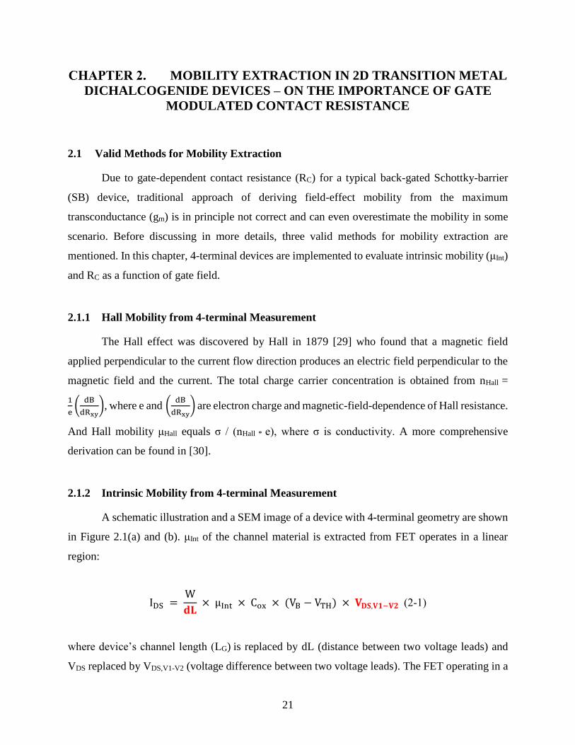
A schematic illustration and a SEM image of a device with 4-terminal geometry are shown
in Figure 2.1(a) and (b). μInt of the channel material is extracted from FET operates in a linear
region:
IDS = W
𝐝𝐋 × μInt × Cox × (VB − VTH) × 𝐕𝐃𝐒,𝐕𝟏−𝐕𝟐 (2-1)
where device’s channel length (LG) is replaced by dL (distance between two voltage leads) and
VDS replaced by VDS,V1-V2 (voltage difference between two voltage leads). The FET operating in a
22
linear region guarantees the carriers are uniformly distributed along the channel so the extracted
μInt is valid to represent the mobility of the devices. By using 4-terminal design, it rules out gate-
dependent SB contact effect when calculating the mobility, which avoids potential overestimation
that is discussed in section 2-3-1.
Figure 2.1 (a) A schematic illustration and (b) scanning electron microscope (SEM) image of a
4-terminal device structure, where LG is the channel length, dL is the distance between two
voltage probes V1 and V2, and Wprobe is the width of each voltage probe.
When only VS and VD electrodes are used together with the gate electrode in the measurement, it
is referred to as 2-terminal measurement.
2.1.3 Transfer Length Measurement from 2-terminal Devices
Another method to extract μInt is by exploiting transfer length measurement (TLM), where
devices of various LG are fabricated on a uniform channel material. The measured total resistance
(RTotal), consisting of contact (RC) and channel resistance (RCH), can be expressed as:
RTotal = 2*RC + RCH = 2*RC + ρshL
W (2-2)
where ρsh is sheet conductance. The key for accurate extractions on ρsh (thus mobility) and RC is
by measuring sufficient devices with enough span of LG, in order to get an accurate linear fitting
from RTotal vs LG plot. Notice that TLM is not suitable for device with large SBH (ex: WSe2) due
(a) (b)
23
to an incorrect threshold voltage (VTH) extracted from linear IDS-VG curves that is typically used
to define device’s VTH. It is discussed further in section 2-3-1.
2.2 Why Extraction from 2-terminal Devices is Not Suitable
The most widespread method for mobility extraction uses the peak transconductance
(gm,max) value to extract the highest field-effect mobility (μFE) from an FET with a source, a drain
and a gate contact (which we will refer to as “2-terminal FET” in the following) in the linear VDS
region employing:
gm
=∂ID
∂VGS
=W
L×μ
FE×Cox×VDS (2-3)
where ID is the drain current, VGS is an applied gate voltage, W/L is device’s channel width/length,
COX is the gate capacitance, and VDS is an applied drain voltage. This approach is valid for Si FETs,
since the highly doped source/drain (S/D) regions in conjunction with metal silicides create low
resistive ohmic contacts [31], [32] and the silicides are not under gate control. However, the story
is more complicated for most TMD-based FETs, where a gate-dependent contact resistance (RC)
arises in a back-gated (BG) device geometry due to a modulation in Schottky-barrier (SB) width
at the source/drain metal-to-channel interface. In addition, a pronounced Fermi-level pinning at
the metal-TMD interface constitutes a main hurdle for realizing a low-resistive contact in the S/D
regions [33]–[36]. Therefore, the common belief is that any contact resistance RC can only impede
the carrier transport and hence always results in an underestimation of μFE extracted from gm,max.
However, it is not a definite case. C. Liu et al. [37] investigated the gate-dependent RC
from simulation which leads to an overestimation of mobility values (although noted that the
concave-like RC vs VGS behavior given in their simulation is not a typical observation from
experimental results due to a screening effect of gate fields). J. R. Nasr et al. [38] revealed the
mobility overestimation by intentionally creating different channel threshold voltages (VTH) in a
dual-gate structure. H.-Y. Chang et al. [39] proposed the Y-function method to remove the RC
effect when evaluating the mobility values. Although the gate-dependent RC is pointed out in above
studies, a comprehensively analysis including the impact of effective oxide thickness (EOT) of the
gate dielectric, different TMD channel materials, and the involvement of extrinsic doping schemes
24
are yet carried out especially from experiments. These are all essential factors that will affect the
threshold voltage identification and the interplay between RC and channel resistance (RCH), which
eventually impact the evaluation of device metrics. It is especially important for devices with a
large SBH, for instance WSe2 where a feature of ambipolar characteristics are typically observe
due to the Fermi-level pinning closer to the middle of the bandgap [40], [41], or for the monolayer
TMDs where a larger bandgap is expected which attributed to a pronounced quantum confinement
[42].
In this chapter, we will first discuss why a careful extraction of the correct, i. e., intrinsic
mobility μint, explicitly mandates the use of a 4-terminal FET geometry for certain TMD FETs, e.
g., WSe2 devices with thick gate dielectrics. We will explain how μFE as defined above can be
larger than actual μint for those types of devices, revealing a rather surprising finding that this
artefact is a result of the contact gating. In this context, it is critical to evaluate the 2-terminal and
4-terminal threshold voltage (VTH_2-terminal and VTH_4-terminal), which can be vastly different for
certain TMD materials and gate dielectrics. In particular, we will also show how μint depends on
the gate voltage, which affects the carrier concentration in the channel. Note that for conventional
CMOS devices, an increase in carrier concentration deep in the device on-state typically implies a
reduction in mobility [17], [18], which is NOT observed in any of our TMD devices. Next, we will
discuss why 2-terminal FET measurements on MoS2 and WS2 (irrespective of gate oxide thickness)
as well as on WSe2 with thin gate dielectrics are adequate to extract intrinsic mobilities with a
moderate error. Lastly, we will discuss how SiNx doping in case of WSe2 devices with a thick gate
dielectric also allows recovering intrinsic device properties.
2.3 Overestimation of Mobility on SB Devices
2.3.1 gm Overestimation from 2-terminal SB Devices
A critical finding of our research is that 2-terminal and 4-terminal FET devices as defined
above can behave vastly different. In order to create our 4-terminal devices, in addition to the
conventional source/drain (VS/VD) contacts, two additional voltage leads (V1 and V2) as shown in
Figure 2.1(a) and (b) were defined, where LG and W are the channel length and channel width,
respectively. We avoid any etching process to create a Hall-bar structure which could potentially
lead to a significant amount of residue on the channel surface, impacting the intrinsic properties of
25
a TMD [43]. Instead, we ensured lithographically that the overlap region between the voltage leads
and the channel is as small as possible to avoid current shunting induced inaccuracies [44]. In
addition, for an accurate extraction of RC and μInt, the width of the voltage leads (Wprobe) needs to
be sufficiently narrow in order to precisely probe the potential profile at one location in the channel
and to identify the distance (dL) between the two voltage leads with a minimal uncertainty. A
similar 4-terminal geometry to evaluate device properties had been employed by in some other
literature as well [45], [46].
As the first example, emphasizing the importance of employing a 4-terminal geometry for
the correct extraction of intrinsic mobilities, we have characterized WSe2 back-gated devices
fabricated on a 90 nm SiO2 on Si substrate – a device configuration commonly used due to
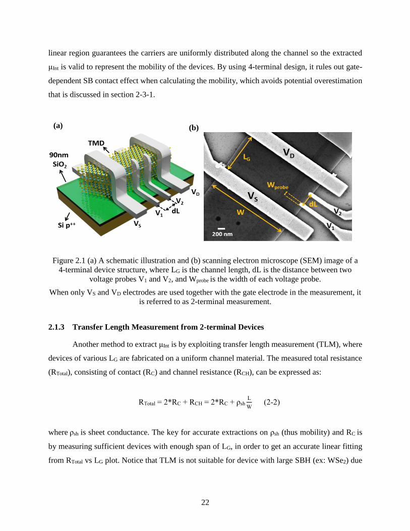
fabrication simplicity. The 4-terminal measurement (see red curve in Figure 2.2(a)) gives direct
access to the normalized channel resistance in the units of Ωμm: 𝑅𝐶𝐻 =𝑉1−𝑉2
𝐼𝐷𝑆∙
𝑊∙𝐿𝐺
𝑑𝐿. RC is then
calculated from (RTotal – RCH) / 2, given RTotal (the 2-terminal resistance) and RCH being measured
experimentally. Figure 2.2(a) presents the dependence of these three resistance values on the back-
gate voltage VBG. Not only does this plot reveal that there is a regime (for small VBG) where RTotal
is dominated by RC, but also shows a stronger dependence of RC than RCH on VBG, which is the
key reason for an overestimation of mobility if gm,max is extracted from 2-terminal measurements.
This point becomes more apparent from Figure 2.2(b) that displays IDS-VBG curves. The “2-
terminal” black curve reveals the change of current impacted by the back-gate dependences of RC
and RCH, while the “4-terminal” red curve presents the channel response after elimination of the
contact resistance contribution through our 4-terminal measurements, i.e., current being calculated
by dividing VDS of 1V by RCH from Figure 2.2(a). As expected, the current level in the 4-terminal
configuration is higher at the same VBG than that from the 2-terminal measurement, since the
contact resistance contribution has been eliminated. Figure 2.2(b) also reveals a steeper slope of
the 2-terminal measurement if compared to the 4-terminal one, which in turn gives rise to a larger
𝑔𝑚 = 𝑑𝐼𝐷𝑆
𝑑𝑉𝐵𝐺|𝑉𝐷𝑆
and, therefore, produces higher mobility value than the correct one associated
with the slope of the 4-terminal curve. The discrepancy stems from the presence of the gate
dependent RC that is part of the 2-terminal measurement. Since RC changes more rapidly with VBG
close to the 2-terminal threshold (VTH_2-terminal), it dominates the gm-extraction, giving rise to an
26
overestimation of mobility. A more detailed analysis concerning the convoluted gm-value in a 2-
terminal geometry is provided in the Appendix 2-6-1.
Another interesting aspect, which is apparent from Figure 2.2(b) is the difference between
the VTH_2-terminal and VTH_4-terminal values. There exists a substantial gate voltage range where the
current in the 2-terminal measurement is suppressed due to RC domination as discussed in the
context of Figure 2.2(a). This discrepancy between VTH_2-terminal and VTH_4-terminal is significant since
the actual amount of charges at a given back gate voltage in the device on-state is indeed 𝑄 = 𝐶𝑜𝑥 ∙
(𝑉𝐵𝐺 − 𝑉𝑇𝐻_4−𝑡𝑒𝑟𝑚𝑖𝑛𝑎𝑙) and thus a smaller Q-value would be extracted using the larger VTH_2-
terminal. An underestimated Q in turn results in an overestimated μ values. Thus, using the classical
2-terminal current equation of a MOSFET in its on-state and gm extracted from a 2-terminal
measurement will both result in systematic errors in the mobility extraction. Instead, the correct
current expression using the 4-terminal configuration should be applied as follows:
ID =W
dL× μint × Cox × (VBG − VTH_4−terminal) × VDS,V1−V2 (2-4)
where dL is the distance between two voltage leads and VDS,V1-V2 is the voltage drop across
them. Figure 2.2(c) compares the extracted 2-terminal and 4-terminal gm-values and Figure 2.2(d)
displays extracted mobility values as a function of overdrive voltage, according to different
extraction methods. In particular, Figure 2.2(d) compares the correct int with extracted μ-values
of the same device, employing gm from 2-terminal measurements (black filled squares) following
the approach from [47]–[50]. Note that different from silicon devices, there is barely any
dependence of int on overdrive voltage. This result is expected, considering that the position of
the electron wave function in the channel above threshold is almost entirely defined by the
geometry, i.e. the ultra-thin TMD body, and the gate voltage has little or no impact on that position.
Open black squares are a result of a method suggested by [51]–[55] that combines gm-values
extracted from 2-terminal measurements with an adjustment of channel voltage drop through their
4-terminal measurement. Note that the latter results in an even larger error and inaccurate gate
voltage dependent trend, which is discussed in greater detail in Appendix 2-6-2. Figure 2.2(e)
illustrates the impact of the metal contact on the carrier distribution in WSe2, which is the cause
for the different VTH-values. Due to Fermi level pinning at the metal contact, there is a depletion
of electrons near the contact region. As a result, when the channel region has reached threshold at
27
VBG=VTH_4-terminal. , the contact region is still below threshold. A larger VBG=VTH_2-terminal is
required to reach VTH in the contact region and enable the electron injection, as shown in the band
diagrams.
Whether the correct VTH has been used when analyzing device data, namely the VTH_4-
terminal, can also be examined by plotting log(RCH) vs. log(VOV) as shown in Figure 2.2(f). A slope
of “-1” is expected if the charge Q in the channel follows the expected 𝐶𝑜𝑥 ∙ (𝑉𝐵𝐺 − 𝑉𝑇𝐻) -
dependence, which is according to our findings always the case when VTH = VTH_4-terminal is used
in the charge expression. On the other hand, if the incorrect VTH_2-terminal is employed for materials
with a large SBH, a “wrong” slope smaller than “-1” will be observed as shown for the black curve.
The above statement is particularly important if using TLM instead of a 4-terminal geometry for
devices with large SBH, where the measurement cannot distinguish between the two different VTH.
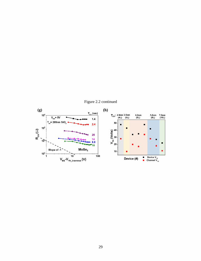
As shown in Figure 2.2(g) where TLM extracted RCH of MoSe2-FETs is displayed for various
channel thickness (TCH), slopes smaller than “-1” for all devices in the log(RCH) vs. log(VOV) plot
are observed. This is a clear evidence of the fact that WSe2 and MoSe2 fall into the same category
of high SBH devices and extra care needs to be taken when analyzing their mobilities. The statistics
of 2-terminal (device) and 4-terminal (channel) VTH are shown in Figure 2.2(h).
To summarize the above findings: Implementation of a 4-terminal geometry is essential to
accurately extract channel mobilities for SB-devices that include a strong gate-dependence of RC.
As we will discuss in the following, large SB heights and thick gate dielectrics as present in WSe2
devices discussed above make the extraction of mobility from 2-terminal measurements
particularly challenging.
28
Figure 2.2 (a) 4-terminal (channel) and 2-terminal (total) as well as contact resistance as a
function of back-gate voltage. (b) Comparison of 2- and 4-terminal IDS-VBG measurements on the
same WSe2 FET, where distinct differences in slope and threshold voltage of the IDS-VBG curves
are observed. (c) Comparison of 2-terminal and 4-terminal transconductance extracted from
Figure 2.2(b). (d) Comparison of the channel mobility values as a function of overdrive voltage
for different extraction methods. (e) Band diagrams of the WSe2 FET at the two threshold
voltages. (f) Log(RCH) vs log(VOV) with different VTH being used. (g) Log(RCH) vs. log(VBG-
VTH_2-terminal) for MoSe2-FETs, showing a slope that is smaller than “-1” for all devices
irrespective of TCH. (h) 2-terminal and 4-terminal VTH for 8 different WSe2 devices on 90nm
SiO2.
(d) (c)
(b) (a)
(f)
29
Figure 2.2 continued
(g) (h)
30
2.3.2 WSe2 Devices Implemented on Thin Dielectric
To further explore the impact of device geometry on mobility extraction, WSe2 FETs were
implemented on thin gate dielectrics. Transfer and output characteristics for a representative device
are shown in Figure 2.3(a) and (b), where steep subthreshold swings (SS) of ~75 mV/dec and
current saturation in the output characteristics are clearly observed. Figure 2.3(c) and (d) display
representative resistance and current curves similar to Figure 2.3(a) and (b). Interestingly, different
from Figure 2.3(a), RC is below RCH for these devices irrespective of the gate voltage. Moreover,
the slopes of the two curves in Figure 2.3(b) are rather similar, implying that similar gm values can
be extracted from the 2-terminal and 4-terminal measurements, as shown in Figure 2.3(e) and (f).
In particular, this suggests that the mobility extraction in the thin dielectric case is much less
sensitive to the measurement method. This experimental observation is the result of a reduced SB
width (λ) at the metal-to-channel interface, which is typically expressed as [56]:
ch ox ch oxλ= (ε /ε )T T
where Tch is the channel thickness, Tox is the oxide thickness, ch and ox are the dielectric
constants of channel and oxide, respectively. SB devices with small λ exhibit similar VTH_2-terminal
and VTH_4-terminal, as illustrated by the example in Figure 2.3(d). In other words, all the effects that
we discussed in the context of WSe2 devices on thick gate dielectrics:
1) there exists a gate voltage range where RC dominates over RCH
2) the slope of IDS vs. VBG curve is substantially smaller in the 4-terminal compared to the 2-
terminal case
3) there is a substantial difference between VTH_2-terminal and VTH_4-terminal
are no longer (or merely) present for the same channel material on a thin back gate dielectric.
The substantially reduced λ for the same SB height eliminates the impact of RC and makes
the difference between the 2-terminal and 4-terminal measurement much less apparent.
Therefore, the peak μFE extracted from a 2-terminal gm is now similar to the correctly
extracted μInt value. However, using the combined 2- and 4-terminal measurement method
[51]–[55] can still overestimate the mobility substantially, as shown Figure 2.3(f).
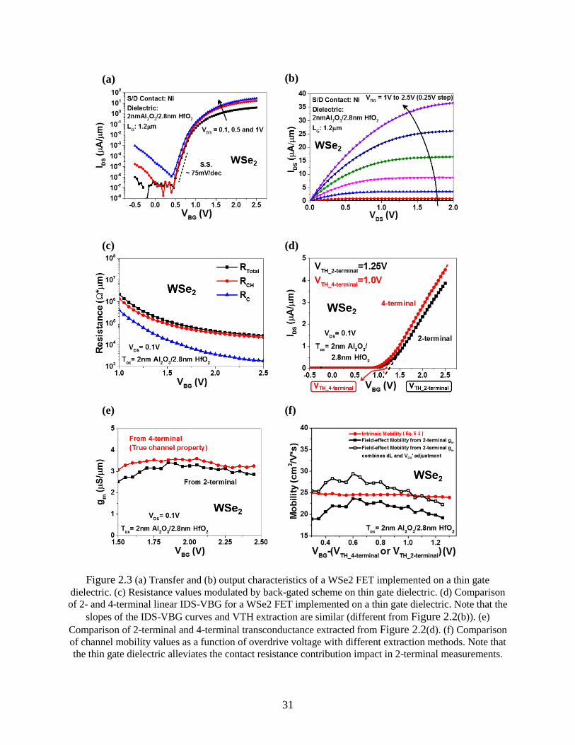
31
Figure 2.3 (a) Transfer and (b) output characteristics of a WSe2 FET implemented on a thin gate
dielectric. (c) Resistance values modulated by back-gated scheme on thin gate dielectric. (d) Comparison
of 2- and 4-terminal linear IDS-VBG for a WSe2 FET implemented on a thin gate dielectric. Note that the
slopes of the IDS-VBG curves and VTH extraction are similar (different from Figure 2.2(b)). (e)
Comparison of 2-terminal and 4-terminal transconductance extracted from Figure 2.2(d). (f) Comparison
of channel mobility values as a function of overdrive voltage with different extraction methods. Note that
the thin gate dielectric alleviates the contact resistance contribution impact in 2-terminal measurements.
(b) (a)
(c) (d)
(e) (f)
32
2.3.3 TMD-based Devices with Smaller Schottky-barrier Height
Up to now, we have focused our attention on WSe2 FETs that exhibit a rather large SBH
for electron injection. From the above discussion about RC, one can expect that reducing the SBH
should result in a similar device behavior as shown in Figure 2.3(d) since both the SB height and
width impact RC. Compared to WSe2, both MoS2 and WS2 exhibit a smaller SBH for electron
injection [7], [57], [58], corroborated by the lack of a hole branch, as shown in Figure 2.4(a) and
(b) comparing to (c). Indeed, MoS2 and WS2 FETs with thick back gate dielectrics do not show
the same discrepancy between 2- and 4-terminal measurements (see Figure 2.4(d) and (e)). Similar
to our discussion about WSe2 devices on thin gate dielectrics, mobility extraction is thus much less
impacted by RC and overestimation of mobility extracted from 2-terminal gm is not a concern in
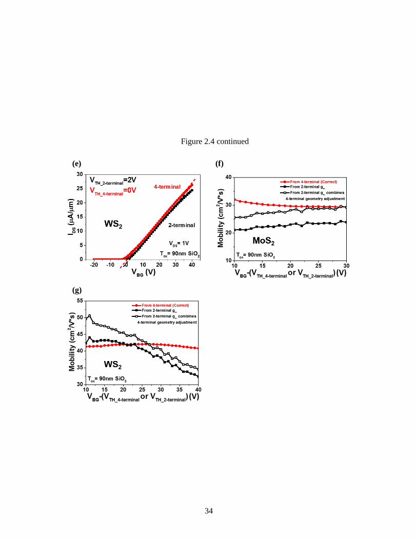
both MoS2 and WS2 devices, as shown in Figure 2.4(f) and (g).
33
Figure 2.4 Transfer characteristics of SB FETs from (a) MoS2, (b) WS2, and (c) WSe2 as
channel material. The lack of hole branch for (a) and (b) indicates that the Fermi-level pinning is
closer to the conduction band for MoS2 and WS2 if compared to WSe2 (and in fact also MoSe2).
(d) Comparison of 2- and 4-terminal linear IDS-VBG for a MoS2 and (e) WS2 FET implemented
on a 90 nm SiO2 gate dielectric. Comparison of channel mobility values as a function of
overdrive voltage with different extraction methods for (f) MoS2 and (g) WS2 FETs implemented
on 90 nm SiO2. Because of the smaller Schottky-barrier heights in cases of MoS2 and WS2
compared to their Se-containing counterparts, even using a 90 nm gate dielectric does not result
in the same mobility extraction issues for these two materials.
(c)
(b) (a)
(d)
34
Figure 2.4 continued
(e) (f)
(g)
35
2.4 Mobility and Contact Resistance vs Gate Field
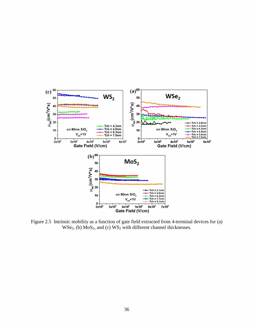
2.4.1 Four-terminal Devices Implemented on 90nm SiO2
μInt of electrons for devices with various channel thicknesses (Tch) are evaluated as a
function of gate field shown in Figure 2.5(a) to (c). we do not observe a discernible channel
thickness-dependence of μInt at room temperature, which is believed to be dominated by phonon
scattering [59]–[61]. We also want to point out that our reported μInt is a lower bound of the actual
mobility due to trapped charges and surface optical phonon scattering as compared to μInt measured
from devices fabricated on a smooth dielectric surface such as hexagonal boron nitride (hBN)
[61]–[63]. WS2 in terms of electron transport is in average the highest, which is in general
consistent with what has been previously reported [63].
RC calculated as (RTotal – RCH)/2 is shown in Figure 2.6 as a function of gate field. Ni is
used as S/D contact in all devices. We observe an increase of RC for thicker flakes compared to
thinner ones for all three TMDs which is attributed to an increase of interlayer resistance for thick
layer, since a typical SB device is gating from the bottom while the S/D contact is fabricated on
the top of a channel material.
36
Figure 2.5 Intrinsic mobility as a function of gate field extracted from 4-terminal devices for (a)
WSe2, (b) MoS2, and (c) WS2 with different channel thicknesses.
37
Figure 2.6 Contact resistance as a function of gate field extracted from 4-terminal devices for (a)
WSe2, (b) MoS2, and (c) WS2 with different channel thicknesses.
2.4.2 Four-terminal Devices Implemented on Thin Dielectric
SB devices with thin dielectric is implemented by e-beam evaporated Cr (3nm) / Au (10nm)
as a local gate followed by 1nm Al seeding layer (turned into ~ 2nm Al2O3 in an air ambient) and
2.8nm HfO2 from ALD as a back-gated dielectric, where the COX is assumed as 1.73 μF/cm2. The
differences between 2-terminal (device) and 4-terminal (channel) VTH are revealed in Figure 2.7.
Comparing VTH offset to WSe2 devices on 90nm SiO2 shown in Figure 2.2(h) a smaller difference
is observed considering Q = COX*VTH-Difference, where COX ~ 38.4nF/cm2 for 90nm SiO2. The more
confined difference between two VTH is attributed to thin dielectric with a smaller EOT that results
in a smaller λ for carriers tunneling through SB, hence a smaller ρC is realized. In addition, the
spreading of VTH-Channel among different devices is smaller due to a significantly less fixed charges
reside in the thin dielectric, which is promising for minimizing VTH variation among devices if the
non-uniformity from the contact can be well-handled. Electron mobility of devices with various
(a) (b)
(c)
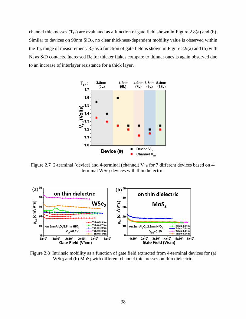
38
channel thicknesses (Tch) are evaluated as a function of gate field shown in Figure 2.8(a) and (b).
Similar to devices on 90nm SiO2, no clear thickness-dependent mobility value is observed within
the Tch range of measurement. RC as a function of gate field is shown in Figure 2.9(a) and (b) with
Ni as S/D contacts. Increased RC for thicker flakes compare to thinner ones is again observed due
to an increase of interlayer resistance for a thick layer.
Figure 2.7 2-terminal (device) and 4-terminal (channel) VTH for 7 different devices based on 4-
terminal WSe2 devices with thin dielectric.
Figure 2.8 Intrinsic mobility as a function of gate field extracted from 4-terminal devices for (a)
WSe2 and (b) MoS2 with different channel thicknesses on thin dielectric.
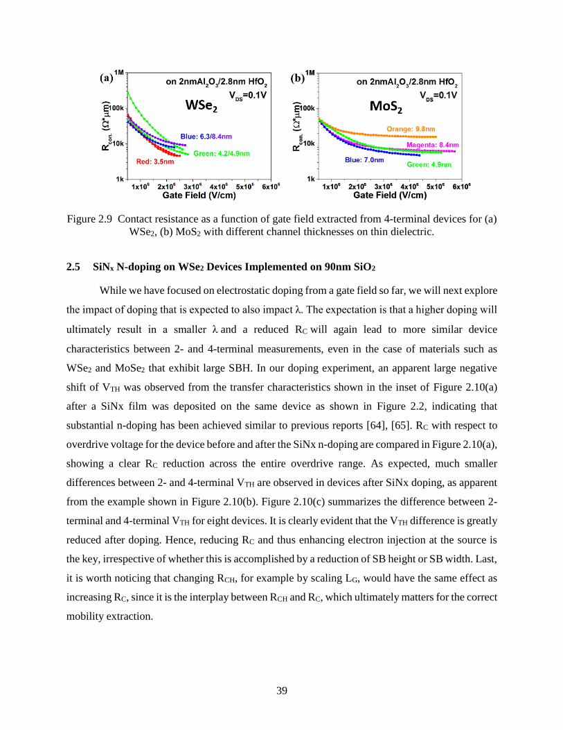
39
Figure 2.9 Contact resistance as a function of gate field extracted from 4-terminal devices for (a)
WSe2, (b) MoS2 with different channel thicknesses on thin dielectric.
2.5 SiNx N-doping on WSe2 Devices Implemented on 90nm SiO2
While we have focused on electrostatic doping from a gate field so far, we will next explore
the impact of doping that is expected to also impact λ. The expectation is that a higher doping will
ultimately result in a smaller λand a reduced RCwill again lead to more similar device
characteristics between 2- and 4-terminal measurements, even in the case of materials such as
WSe2 and MoSe2 that exhibit large SBH. In our doping experiment, an apparent large negative
shift of VTH was observed from the transfer characteristics shown in the inset of Figure 2.10(a)
after a SiNx film was deposited on the same device as shown in Figure 2.2, indicating that
substantial n-doping has been achieved similar to previous reports [64], [65]. RC with respect to
overdrive voltage for the device before and after the SiNx n-doping are compared in Figure 2.10(a),
showing a clear RC reduction across the entire overdrive range. As expected, much smaller
differences between 2- and 4-terminal VTH are observed in devices after SiNx doping, as apparent
from the example shown in Figure 2.10(b). Figure 2.10(c) summarizes the difference between 2-
terminal and 4-terminal VTH for eight devices. It is clearly evident that the VTH difference is greatly
reduced after doping. Hence, reducing RC and thus enhancing electron injection at the source is
the key, irrespective of whether this is accomplished by a reduction of SB height or SB width. Last,
it is worth noticing that changing RCH, for example by scaling LG, would have the same effect as
increasing RC, since it is the interplay between RCH and RC, which ultimately matters for the correct
mobility extraction.
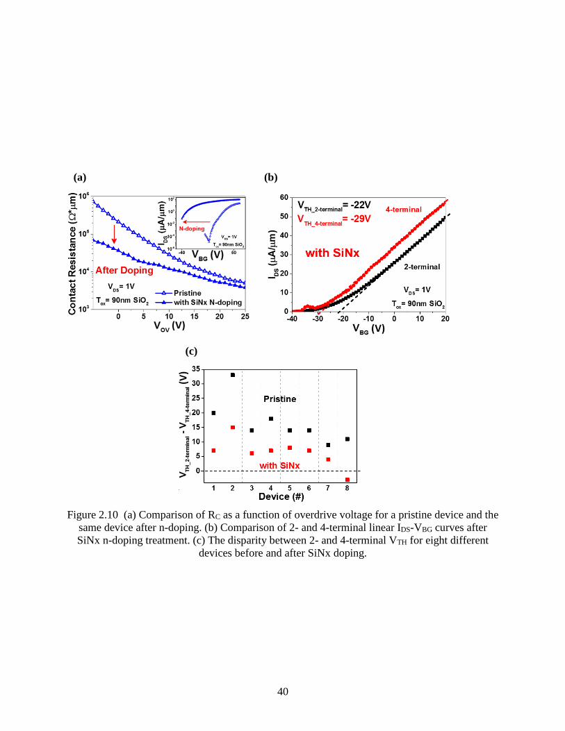
40
Figure 2.10 (a) Comparison of RC as a function of overdrive voltage for a pristine device and the
same device after n-doping. (b) Comparison of 2- and 4-terminal linear IDS-VBG curves after
SiNx n-doping treatment. (c) The disparity between 2- and 4-terminal VTH for eight different
devices before and after SiNx doping.
(a) (b)
(c)
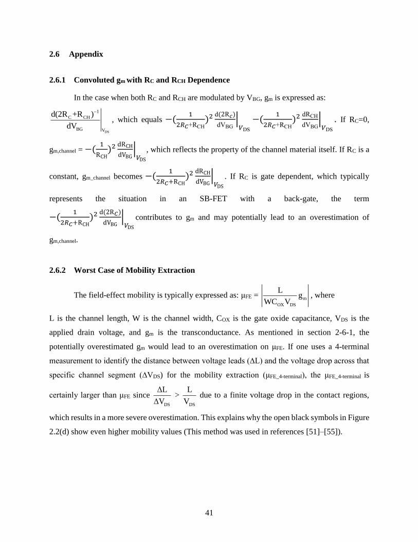
41
2.6 Appendix
2.6.1 Convoluted gm with RC and RCH Dependence
In the case when both RC and RCH are modulated by VBG, gm is expressed as:
DS
1
C CH
BG V
d(2R +R )
dV
, which equals −(1
2𝑅𝐶+RCH)2 d(2R𝑐)
dVBG|
𝑉DS
−(1
2𝑅𝐶+RCH)2 dRCH
dVBG|
𝑉DS
. If RC=0,
gm,channel = −(1
RCH)2 dRCH
dVBG|
𝑉DS
, which reflects the property of the channel material itself. If RC is a
constant, gm_channel becomes −(1
2𝑅𝐶+RCH)2 dRCH
dVBG|
𝑉DS
. If RC is gate dependent, which typically
represents the situation in an SB-FET with a back-gate, the term
−(1
2𝑅𝐶+RCH)2 d(2R𝐶)
dVBG|
𝑉DS
contributes to gm and may potentially lead to an overestimation of
gm,channel.
2.6.2 Worst Case of Mobility Extraction
The field-effect mobility is typically expressed as: μFE = m
OX DS
Lg
WC V, where
L is the channel length, W is the channel width, COX is the gate oxide capacitance, VDS is the
applied drain voltage, and gm is the transconductance. As mentioned in section 2-6-1, the
potentially overestimated gm would lead to an overestimation on μFE. If one uses a 4-terminal
measurement to identify the distance between voltage leads (∆L) and the voltage drop across that
specific channel segment (∆VDS) for the mobility extraction (μFE_4-terminal), the μFE_4-terminal is
certainly larger than μFE since DS
ΔL
ΔV >
DS
L
V due to a finite voltage drop in the contact regions,
which results in a more severe overestimation. This explains why the open black symbols in Figure
2.2(d) show even higher mobility values (This method was used in references [51]–[55]).
42
2.7 Conclusion
A comprehensive study on the mobility of four different TMD channel materials, i.e. MoS2,
WS2, MoSe2, and WSe2 has been presented. Particular attention has been paid to the importance
of performing 4-terminal device measurements if contact resistances are large compared to the
channel resistance. Interestingly, the mobility values extracted from 2-terminal gm-measurements
may suffer from potential overestimation, especially for devices with a large SB height associated
with Fermi-level pinning. An obvious disparity of 2- and 4-terminal VTH is observed in these
devices. This phenomenon is attributed to a large RC if compared with RCH and can be partially
mitigated in devices with a thin gate dielectric or intentionally doped FET channel. Our work also
revealed that μInt is rather insensitive to the gate field.
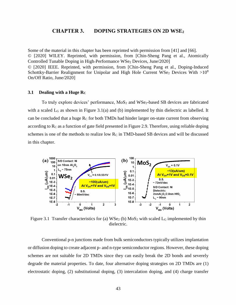
43
DOPING STRATEGIES ON 2D WSE2
Some of the material in this chapter has been reprinted with permission from [41] and [66].
© [2020] WILEY. Reprinted, with permission, from [Chin-Sheng Pang et al., Atomically
Controlled Tunable Doping in High‐Performance WSe2 Devices, June/2020]
© [2020] IEEE. Reprinted, with permission, from [Chin-Sheng Pang et al., Doping-Induced
Schottky-Barrier Realignment for Unipolar and High Hole Current WSe2 Devices With >108
On/Off Ratio, June/2020]
3.1 Dealing with a Huge RC
To truly explore devices’ performance, MoS2 and WSe2-based SB devices are fabricated
with a scaled LG as shown in Figure 3.1(a) and (b) implemented by thin dielectric as labelled. It
can be concluded that a huge RC for both TMDs had hinder larger on-state current from observing
according to RC as a function of gate field presented in Figure 2.9. Therefore, using reliable doping
schemes is one of the methods to realize low RC in TMD-based SB devices and will be discussed
in this chapter.
Figure 3.1 Transfer characteristics for (a) WSe2 (b) MoS2 with scaled LG implemented by thin
dielectric.
Conventional p-n junctions made from bulk semiconductors typically utilizes implantation
or diffusion doping to create adjacent p- and n-type semiconductor regions. However, these doping
schemes are not suitable for 2D TMDs since they can easily break the 2D bonds and severely
degrade the material properties. To date, four alternative doping strategies on 2D TMDs are (1)
electrostatic doping, (2) substitutional doping, (3) intercalation doping, and (4) charge transfer
44
doping. TMDs are specifically susceptible to electrostatic control due to their atomically thin
channel by nature. The advantages of non-destructive and reconfigurable properties through
capacitance coupling between gate and channel are expected to manifest itself in otherwise
unattainable doping scheme. However, more complicated structures will be expected which leads
to potential penalties of higher parasitic capacitance and larger footprint. Substitutional doping
through replacing host atoms with either cationic or anionic elements in TMDs can create n- or p-
type conductance depending on the numbers of valence electrons from the dopants [67]–[69].
Nevertheless, it is difficult to achieve a doping within selective regions since the dopants are
usually applied in situ during the growth process. Intercalation doping is commonly performed
through solution-based processing [70]–[72], which is not a semiconductor industrial-favored
method. Charge transfer doping utilizes interaction between host and adjacent mediums [73]–[75],
which avoids lattice distortion and preserves high mobility transport in TMDs. However, some of
the dopants are volatile in air which have their own scientific interests but not desired for practical
applications. Comprehensive discussions can be found in the review literature [76]
Besides channel doping for better conductance, a rather large contact resistance (RC) due
to SB contact remains a big challenge for TMD FETs, while it is widely acknowledged that
minimizing RC is essential to obtain high performance devices and to reveal intrinsic TMD
properties [73], [74], [77]. In general, there are two strategies to optimize current injection at a
metal-semiconductor (MS) interface. One method is to select a metal contact with the preferred
work function for electron or hole injection, given no strong Fermi level pinning at the contact
interface, which is typically not the case for TMDs [33]–[35]. The other method is to dope the
semiconductor degenerately to reduce the depletion width of the MS junction [64], [73]–[75].
From our study, we believe some specific doping schemes (ex: O2-plasma treatment on WSe2)
could modulate the MS interface property, leading to a reduced RC and to achieve high-
performance SB devices.
In this chapter, we evaluate three industrial compatible doping processes on WSe2 devices
including SiNx passivation for n-doping, O2-plasma treatment for tunable p-doping, and nitric
oxide annealing for p-doping. Reduced RC is extracted from 4-terminal devices measurement,
facilitating n-/p-type MOSFET and high-performance SB devices with scaled LG.
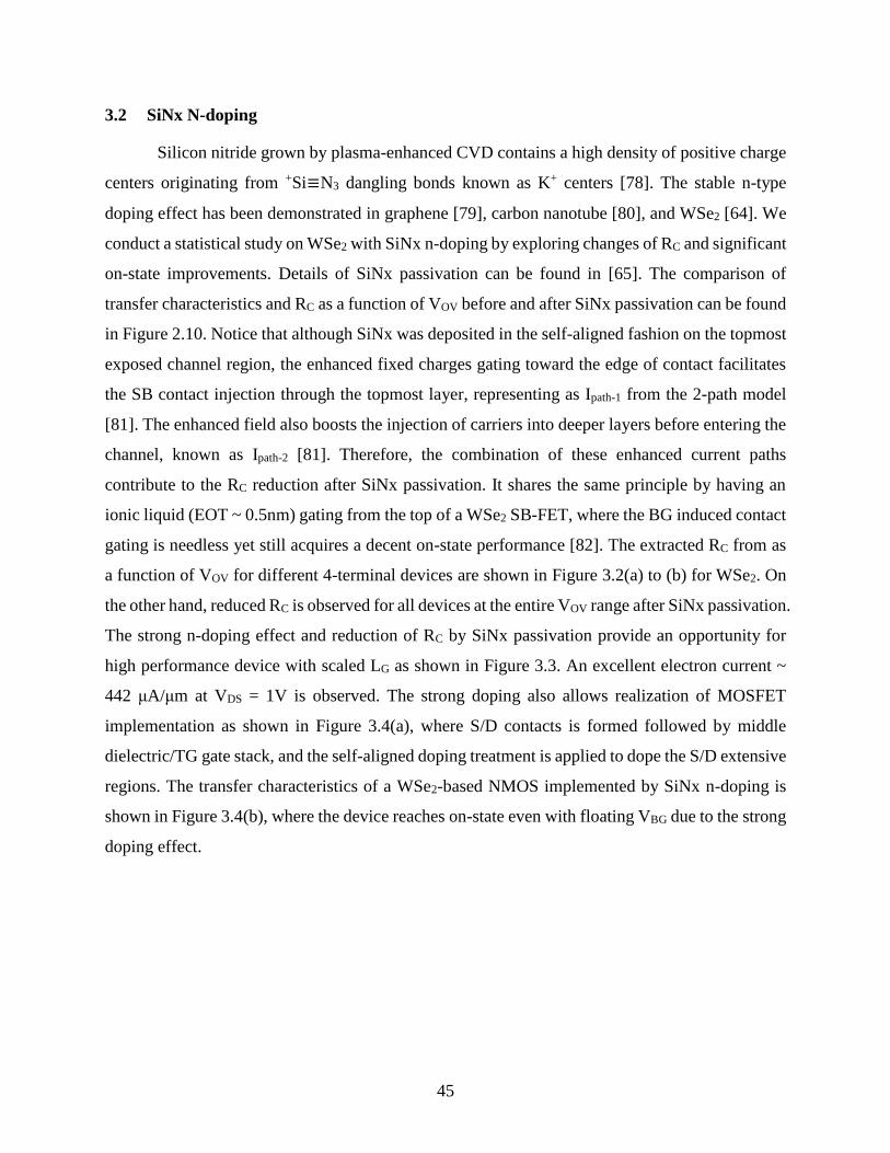
45
3.2 SiNx N-doping
Silicon nitride grown by plasma-enhanced CVD contains a high density of positive charge
centers originating from +Si≡N3 dangling bonds known as K+ centers [78]. The stable n-type
doping effect has been demonstrated in graphene [79], carbon nanotube [80], and WSe2 [64]. We
conduct a statistical study on WSe2 with SiNx n-doping by exploring changes of RC and significant
on-state improvements. Details of SiNx passivation can be found in [65]. The comparison of
transfer characteristics and RC as a function of VOV before and after SiNx passivation can be found
in Figure 2.10. Notice that although SiNx was deposited in the self-aligned fashion on the topmost
exposed channel region, the enhanced fixed charges gating toward the edge of contact facilitates
the SB contact injection through the topmost layer, representing as Ipath-1 from the 2-path model
[81]. The enhanced field also boosts the injection of carriers into deeper layers before entering the
channel, known as Ipath-2 [81]. Therefore, the combination of these enhanced current paths
contribute to the RC reduction after SiNx passivation. It shares the same principle by having an
ionic liquid (EOT ~ 0.5nm) gating from the top of a WSe2 SB-FET, where the BG induced contact
gating is needless yet still acquires a decent on-state performance [82]. The extracted RC from as
a function of VOV for different 4-terminal devices are shown in Figure 3.2(a) to (b) for WSe2. On
the other hand, reduced RC is observed for all devices at the entire VOV range after SiNx passivation.
The strong n-doping effect and reduction of RC by SiNx passivation provide an opportunity for
high performance device with scaled LG as shown in Figure 3.3. An excellent electron current ~
442 μA/μm at VDS = 1V is observed. The strong doping also allows realization of MOSFET
implementation as shown in Figure 3.4(a), where S/D contacts is formed followed by middle
dielectric/TG gate stack, and the self-aligned doping treatment is applied to dope the S/D extensive
regions. The transfer characteristics of a WSe2-based NMOS implemented by SiNx n-doping is
shown in Figure 3.4(b), where the device reaches on-state even with floating VBG due to the strong
doping effect.
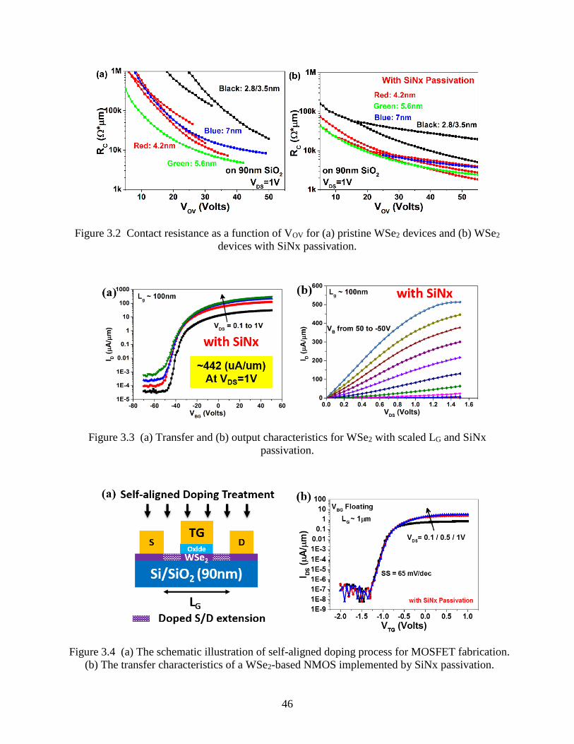
46
Figure 3.2 Contact resistance as a function of VOV for (a) pristine WSe2 devices and (b) WSe2
devices with SiNx passivation.
Figure 3.3 (a) Transfer and (b) output characteristics for WSe2 with scaled LG and SiNx
passivation.
Figure 3.4 (a) The schematic illustration of self-aligned doping process for MOSFET fabrication.
(b) The transfer characteristics of a WSe2-based NMOS implemented by SiNx passivation.
47
3.3 O2-plasma P-doping
3.3.1 Temperature-dependent Tunable Doping Scheme
Using O2-plasma to achieve a non-degenerate p-doping and atomically one-layered
conversion on WSe2 has been first shown in [47] and [83]. The p-doping is due to the formation
of WO3-x that is having a high electron affinity [84].In our research, different from the previously
reported self-limiting oxidation of only the topmost WSe2 layer in a remote plasma environment
[47], a direct O2-plasma is employed in our process. Interestingly, we found that the doping level
can be tuned from non-degenerate to degenerate by increasing the treatment temperature which
directly controls the number of WSe2 layers that get converted into WO3-x (0 < x < 1). Moreover,
this conversion is found to extend into the contact area by tens of nanometers, which can possibly
unpin the Fermi level of the metal contact and dope a small segment of WSe2 underneath the
contact, resulting in reduced contact resistance of the device. In additional, SB devices with
excellent hole current of ~ 320 μA/μm at VDS = -1V and PMOS with high air stability are achieved
as well.
To observe different layers conversion of WSe2, different samples were exposed to a direct
O2-plasma at various conditions. Simply comparing color contrast of the samples before and after
exposure under an optical microscope as shown in Figure 3.5, it was rather clear that process
temperature is more effective than plasma power or exposure time in controlling the WSe2
oxidation process. Raman spectra of three sets of pristine bi-layer and tri-layer CVD WSe2 samples
are presented in the top panels of Figure 3.6(a) and (b). Consistent with previous reports [85], the
1B2g Raman mode at 310 cm-1 only appears in multi-layers and bulk WSe2 but does not show up in
monolayers. In the bottom panel of Figure 3.6(a), the 1B2g peak vanished after the room
temperature (RT) O2-plasma treatment on all three bi-layer samples, indicating that only the
bottom WSe2 layer was left while the top layer was oxidized. In contrast, the 310 cm-1 peak
remained in the spectra for all three tri-layer samples (bottom panel of Figure 3.6(b)), suggesting
that only the top layer was converted to oxide while the bottom two layers were intact after the RT
treatment. Interestingly, when the temperature was raised to 150oC, no Raman peaks were
observed in bilayer samples after the treatment. We conclude that both layers were converted into
WO3-x. Therefore, different from the RT treatment, more than one layer of WSe2 can be converted
by O2-plasma at elevated temperatures.
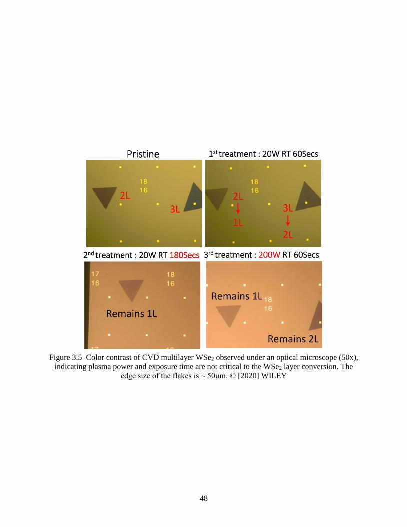
48
Figure 3.5 Color contrast of CVD multilayer WSe2 observed under an optical microscope (50x),
indicating plasma power and exposure time are not critical to the WSe2 layer conversion. The
edge size of the flakes is ~ 50μm. © [2020] WILEY
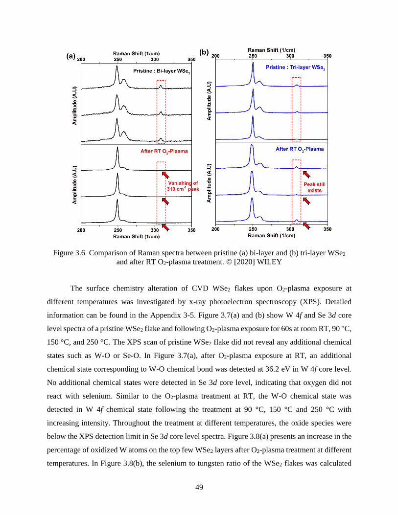
49
Figure 3.6 Comparison of Raman spectra between pristine (a) bi-layer and (b) tri-layer WSe2
and after RT O2-plasma treatment. © [2020] WILEY
The surface chemistry alteration of CVD WSe2 flakes upon O2-plasma exposure at
different temperatures was investigated by x-ray photoelectron spectroscopy (XPS). Detailed
information can be found in the Appendix 3-5. Figure 3.7(a) and (b) show W 4f and Se 3d core
level spectra of a pristine WSe2 flake and following O2-plasma exposure for 60s at room RT, 90 °C,
150 °C, and 250 °C. The XPS scan of pristine WSe2 flake did not reveal any additional chemical
states such as W-O or Se-O. In Figure 3.7(a), after O2-plasma exposure at RT, an additional
chemical state corresponding to W-O chemical bond was detected at 36.2 eV in W 4f core level.
No additional chemical states were detected in Se 3d core level, indicating that oxygen did not
react with selenium. Similar to the O2-plasma treatment at RT, the W-O chemical state was
detected in W 4f chemical state following the treatment at 90 °C, 150 °C and 250 °C with
increasing intensity. Throughout the treatment at different temperatures, the oxide species were
below the XPS detection limit in Se 3d core level spectra. Figure 3.8(a) presents an increase in the
percentage of oxidized W atoms on the top few WSe2 layers after O2-plasma treatment at different
temperatures. In Figure 3.8(b), the selenium to tungsten ratio of the WSe2 flakes was calculated
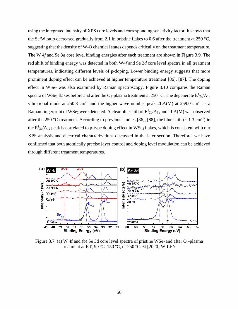
50
using the integrated intensity of XPS core levels and corresponding sensitivity factor. It shows that
the Se/W ratio decreased gradually from 2.1 in pristine flakes to 0.6 after the treatment at 250 °C,
suggesting that the density of W-O chemical states depends critically on the treatment temperature.
The W 4f and Se 3d core level binding energies after each treatment are shown in Figure 3.9. The
red shift of binding energy was detected in both W4f and Se 3d core level spectra in all treatment
temperatures, indicating different levels of p-doping. Lower binding energy suggests that more
prominent doping effect can be achieved at higher temperature treatment [86], [87]. The doping
effect in WSe2 was also examined by Raman spectroscopy. Figure 3.10 compares the Raman
spectra of WSe2 flakes before and after the O2-plasma treatment at 250 °C. The degenerate E12g/A1g
vibrational mode at 250.8 cm-1 and the higher wave number peak 2LA(M) at 259.0 cm-1 as a
Raman fingerprint of WSe2 were detected. A clear blue shift of E12g/A1g and 2LA(M) was observed
after the 250 °C treatment. According to previous studies [86], [88], the blue shift (~ 1.3 cm-1) in
the E12g/A1g peak is correlated to p-type doping effect in WSe2 flakes, which is consistent with our
XPS analysis and electrical characterizations discussed in the later section. Therefore, we have
confirmed that both atomically precise layer control and doping level modulation can be achieved
through different treatment temperatures.
Figure 3.7 (a) W 4f and (b) Se 3d core level spectra of pristine WSe2 and after O2-plasma
treatment at RT, 90 oC, 150 oC, or 250 oC. © [2020] WILEY
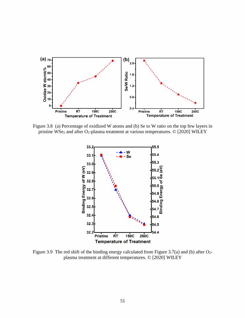
51
Figure 3.8 (a) Percentage of oxidized W atoms and (b) Se to W ratio on the top few layers in
pristine WSe2 and after O2-plasma treatment at various temperatures. © [2020] WILEY
Figure 3.9 The red shift of the binding energy calculated from Figure 3.7(a) and (b) after O2-
plasma treatment at different temperatures. © [2020] WILEY
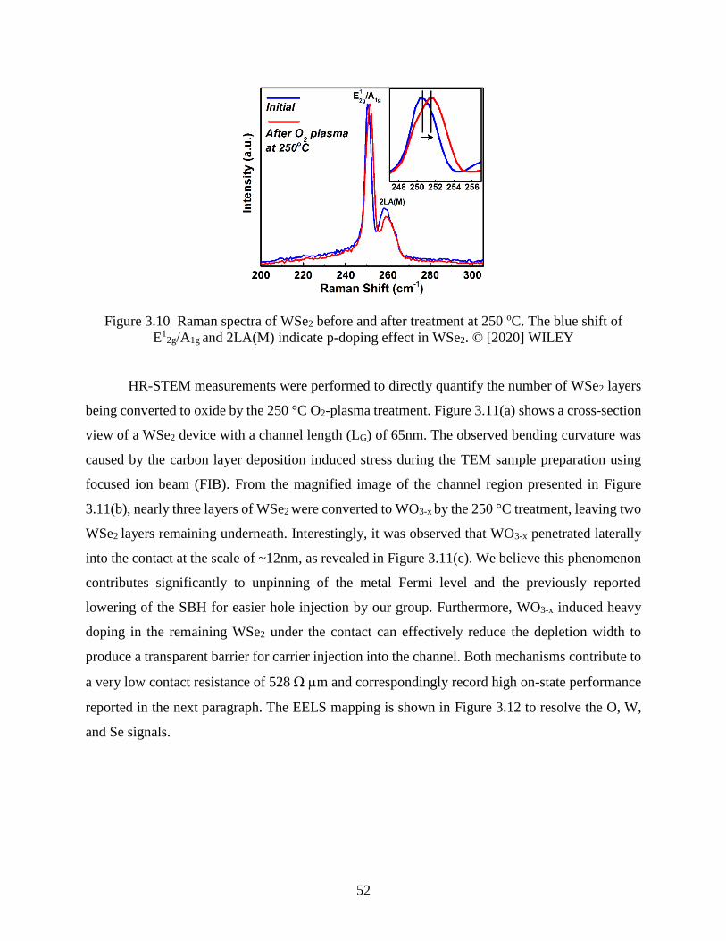
52
Figure 3.10 Raman spectra of WSe2 before and after treatment at 250 oC. The blue shift of
E12g/A1g and 2LA(M) indicate p-doping effect in WSe2. © [2020] WILEY
HR-STEM measurements were performed to directly quantify the number of WSe2 layers
being converted to oxide by the 250 °C O2-plasma treatment. Figure 3.11(a) shows a cross-section
view of a WSe2 device with a channel length (LG) of 65nm. The observed bending curvature was
caused by the carbon layer deposition induced stress during the TEM sample preparation using
focused ion beam (FIB). From the magnified image of the channel region presented in Figure
3.11(b), nearly three layers of WSe2 were converted to WO3-x by the 250 °C treatment, leaving two
WSe2 layers remaining underneath. Interestingly, it was observed that WO3-x penetrated laterally
into the contact at the scale of ~12nm, as revealed in Figure 3.11(c). We believe this phenomenon
contributes significantly to unpinning of the metal Fermi level and the previously reported
lowering of the SBH for easier hole injection by our group. Furthermore, WO3-x induced heavy
doping in the remaining WSe2 under the contact can effectively reduce the depletion width to
produce a transparent barrier for carrier injection into the channel. Both mechanisms contribute to
a very low contact resistance of 528 m and correspondingly record high on-state performance
reported in the next paragraph. The EELS mapping is shown in Figure 3.12 to resolve the O, W,
and Se signals.
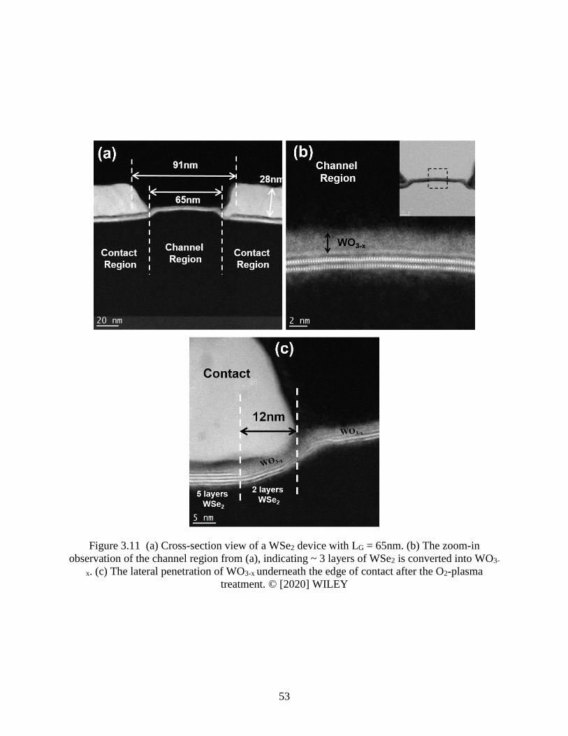
53
Figure 3.11 (a) Cross-section view of a WSe2 device with LG = 65nm. (b) The zoom-in
observation of the channel region from (a), indicating ~ 3 layers of WSe2 is converted into WO3-
x. (c) The lateral penetration of WO3-x underneath the edge of contact after the O2-plasma
treatment. © [2020] WILEY
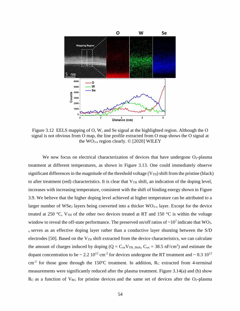
54
Figure 3.12 EELS mapping of O, W, and Se signal at the highlighted region. Although the O
signal is not obvious from O map, the line profile extracted from O map shows the O signal at
the WO3-x region clearly. © [2020] WILEY
We now focus on electrical characterization of devices that have undergone O2-plasma
treatment at different temperatures, as shown in Figure 3.13. One could immediately observe
significant differences in the magnitude of the threshold voltage (VTH) shift from the pristine (black)
to after treatment (red) characteristics. It is clear that VTH shift, an indication of the doping level,
increases with increasing temperature, consistent with the shift of binding energy shown in Figure
3.9. We believe that the higher doping level achieved at higher temperature can be attributed to a
larger number of WSe2 layers being converted into a thicker WO3-x layer. Except for the device
treated at 250 °C, VTH of the other two devices treated at RT and 150 °C is within the voltage
window to reveal the off-state performance. The preserved on/off ratios of ~107 indicate that WO3-
x serves as an effective doping layer rather than a conductive layer shunting between the S/D
electrodes [50]. Based on the VTH shift extracted from the device characteristics, we can calculate
the amount of charges induced by doping (Q = CoxVTH_Shift, Cox = 38.5 nF/cm2) and estimate the
dopant concentration to be ~ 2.2 1012 cm-2 for devices undergone the RT treatment and ~ 8.3 1012
cm-2 for those gone through the 150oC treatment. In addition, RC extracted from 4-terminal
measurements were significantly reduced after the plasma treatment. Figure 3.14(a) and (b) show
RC as a function of VBG for pristine devices and the same set of devices after the O2-plasma
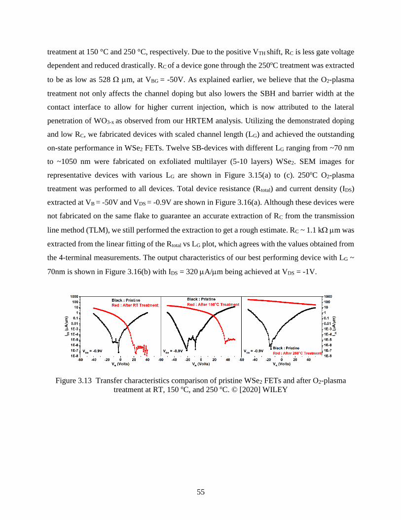
55
treatment at 150 °C and 250 °C, respectively. Due to the positive VTH shift, RC is less gate voltage
dependent and reduced drastically. RC of a device gone through the 250oC treatment was extracted
to be as low as 528 m, at VBG = -50V. As explained earlier, we believe that the O2-plasma
treatment not only affects the channel doping but also lowers the SBH and barrier width at the
contact interface to allow for higher current injection, which is now attributed to the lateral
penetration of WO3-x as observed from our HRTEM analysis. Utilizing the demonstrated doping
and low RC, we fabricated devices with scaled channel length (LG) and achieved the outstanding
on-state performance in WSe2 FETs. Twelve SB-devices with different LG ranging from ~70 nm
to ~1050 nm were fabricated on exfoliated multilayer (5-10 layers) WSe2. SEM images for
representative devices with various LG are shown in Figure 3.15(a) to (c). 250oC O2-plasma
treatment was performed to all devices. Total device resistance (Rtotal) and current density (IDS)
extracted at VB = -50V and VDS = -0.9V are shown in Figure 3.16(a). Although these devices were
not fabricated on the same flake to guarantee an accurate extraction of RC from the transmission
line method (TLM), we still performed the extraction to get a rough estimate. RC ~ 1.1 k m was
extracted from the linear fitting of the Rtotal vs LG plot, which agrees with the values obtained from
the 4-terminal measurements. The output characteristics of our best performing device with LG ~
70nm is shown in Figure 3.16(b) with IDS = 320 A/m being achieved at VDS = -1V.
Figure 3.13 Transfer characteristics comparison of pristine WSe2 FETs and after O2-plasma
treatment at RT, 150 oC, and 250 oC. © [2020] WILEY
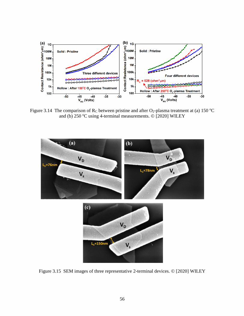
56
Figure 3.14 The comparison of RC between pristine and after O2-plasma treatment at (a) 150 oC
and (b) 250 oC using 4-terminal measurements. © [2020] WILEY
Figure 3.15 SEM images of three representative 2-terminal devices. © [2020] WILEY
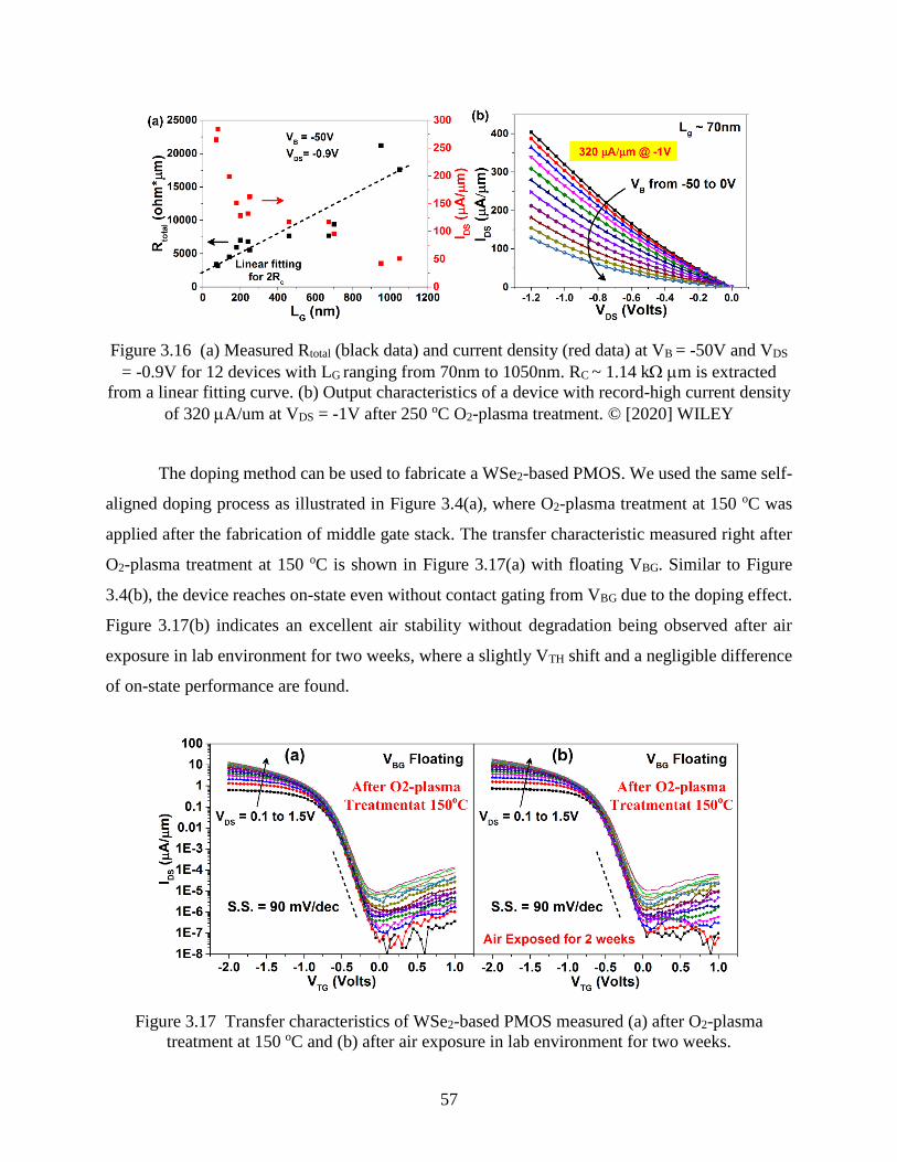
57
Figure 3.16 (a) Measured Rtotal (black data) and current density (red data) at VB = -50V and VDS
= -0.9V for 12 devices with LG ranging from 70nm to 1050nm. RC ~ 1.14 k m is extracted
from a linear fitting curve. (b) Output characteristics of a device with record-high current density
of 320 A/um at VDS = -1V after 250 oC O2-plasma treatment. © [2020] WILEY
The doping method can be used to fabricate a WSe2-based PMOS. We used the same self-
aligned doping process as illustrated in Figure 3.4(a), where O2-plasma treatment at 150 oC was
applied after the fabrication of middle gate stack. The transfer characteristic measured right after
O2-plasma treatment at 150 oC is shown in Figure 3.17(a) with floating VBG. Similar to Figure
3.4(b), the device reaches on-state even without contact gating from VBG due to the doping effect.
Figure 3.17(b) indicates an excellent air stability without degradation being observed after air
exposure in lab environment for two weeks, where a slightly VTH shift and a negligible difference
of on-state performance are found.
Figure 3.17 Transfer characteristics of WSe2-based PMOS measured (a) after O2-plasma
treatment at 150 oC and (b) after air exposure in lab environment for two weeks.
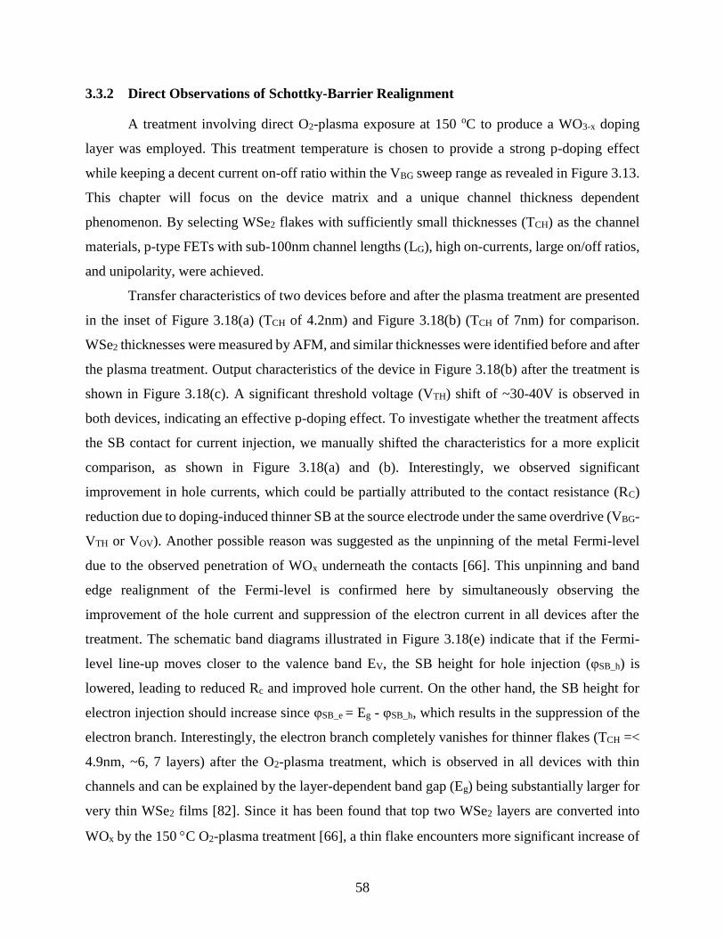
58
3.3.2 Direct Observations of Schottky-Barrier Realignment
A treatment involving direct O2-plasma exposure at 150 oC to produce a WO3-x doping
layer was employed. This treatment temperature is chosen to provide a strong p-doping effect
while keeping a decent current on-off ratio within the VBG sweep range as revealed in Figure 3.13.
This chapter will focus on the device matrix and a unique channel thickness dependent
phenomenon. By selecting WSe2 flakes with sufficiently small thicknesses (TCH) as the channel
materials, p-type FETs with sub-100nm channel lengths (LG), high on-currents, large on/off ratios,
and unipolarity, were achieved.
Transfer characteristics of two devices before and after the plasma treatment are presented
in the inset of Figure 3.18(a) (TCH of 4.2nm) and Figure 3.18(b) (TCH of 7nm) for comparison.
WSe2 thicknesses were measured by AFM, and similar thicknesses were identified before and after
the plasma treatment. Output characteristics of the device in Figure 3.18(b) after the treatment is
shown in Figure 3.18(c). A significant threshold voltage (VTH) shift of ~30-40V is observed in
both devices, indicating an effective p-doping effect. To investigate whether the treatment affects
the SB contact for current injection, we manually shifted the characteristics for a more explicit
comparison, as shown in Figure 3.18(a) and (b). Interestingly, we observed significant
improvement in hole currents, which could be partially attributed to the contact resistance (RC)
reduction due to doping-induced thinner SB at the source electrode under the same overdrive (VBG-
VTH or VOV). Another possible reason was suggested as the unpinning of the metal Fermi-level
due to the observed penetration of WOx underneath the contacts [66]. This unpinning and band
edge realignment of the Fermi-level is confirmed here by simultaneously observing the
improvement of the hole current and suppression of the electron current in all devices after the
treatment. The schematic band diagrams illustrated in Figure 3.18(e) indicate that if the Fermi-
level line-up moves closer to the valence band EV, the SB height for hole injection (φSB_h) is
lowered, leading to reduced Rc and improved hole current. On the other hand, the SB height for
electron injection should increase since φSB_e = Eg - φSB_h, which results in the suppression of the
electron branch. Interestingly, the electron branch completely vanishes for thinner flakes (TCH =<
4.9nm, ~6, 7 layers) after the O2-plasma treatment, which is observed in all devices with thin
channels and can be explained by the layer-dependent band gap (Eg) being substantially larger for
very thin WSe2 films [82]. Since it has been found that top two WSe2 layers are converted into
WOx by the 150 C O2-plasma treatment [66], a thin flake encounters more significant increase of
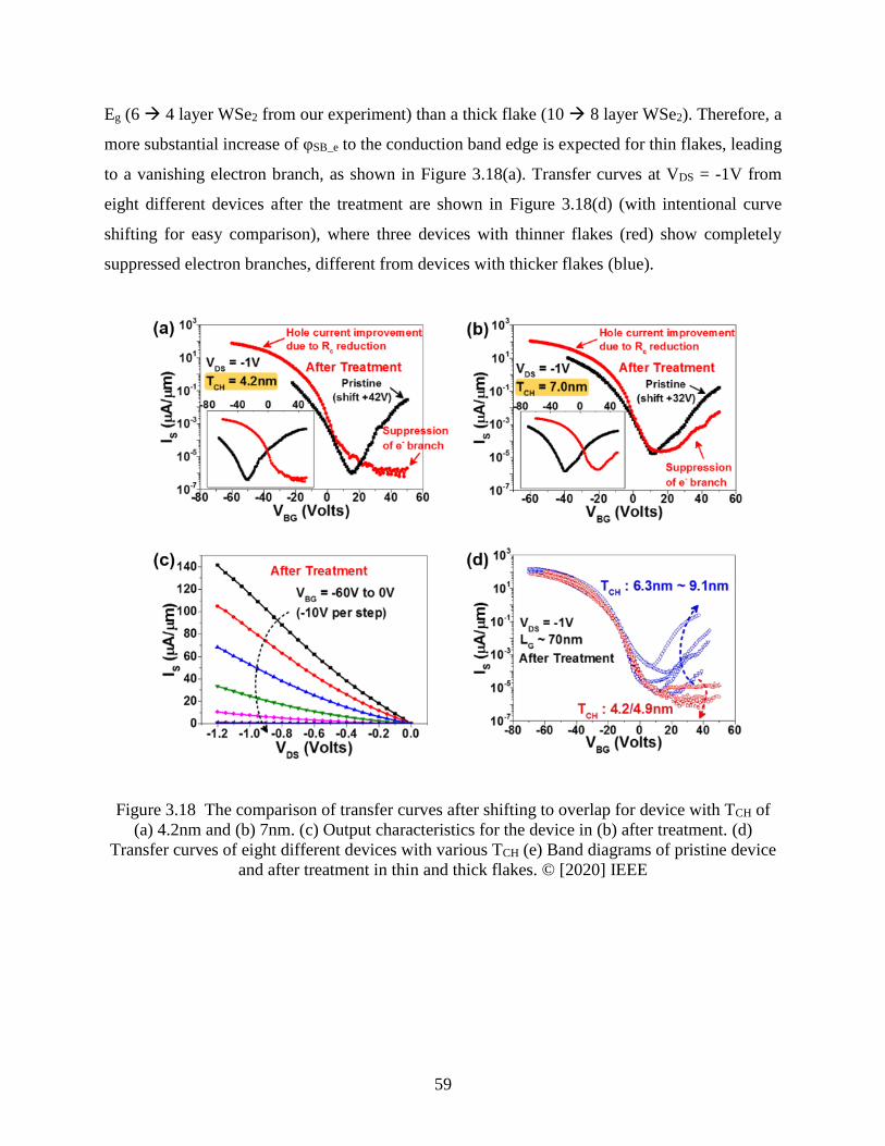
59
Eg (6 4 layer WSe2 from our experiment) than a thick flake (10 8 layer WSe2). Therefore, a
more substantial increase of φSB_e to the conduction band edge is expected for thin flakes, leading
to a vanishing electron branch, as shown in Figure 3.18(a). Transfer curves at VDS = -1V from
eight different devices after the treatment are shown in Figure 3.18(d) (with intentional curve
shifting for easy comparison), where three devices with thinner flakes (red) show completely
suppressed electron branches, different from devices with thicker flakes (blue).
Figure 3.18 The comparison of transfer curves after shifting to overlap for device with TCH of
(a) 4.2nm and (b) 7nm. (c) Output characteristics for the device in (b) after treatment. (d)
Transfer curves of eight different devices with various TCH (e) Band diagrams of pristine device
and after treatment in thin and thick flakes. © [2020] IEEE
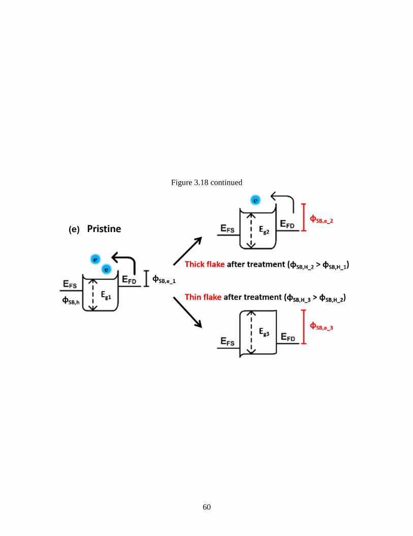
60
Figure 3.18 continued
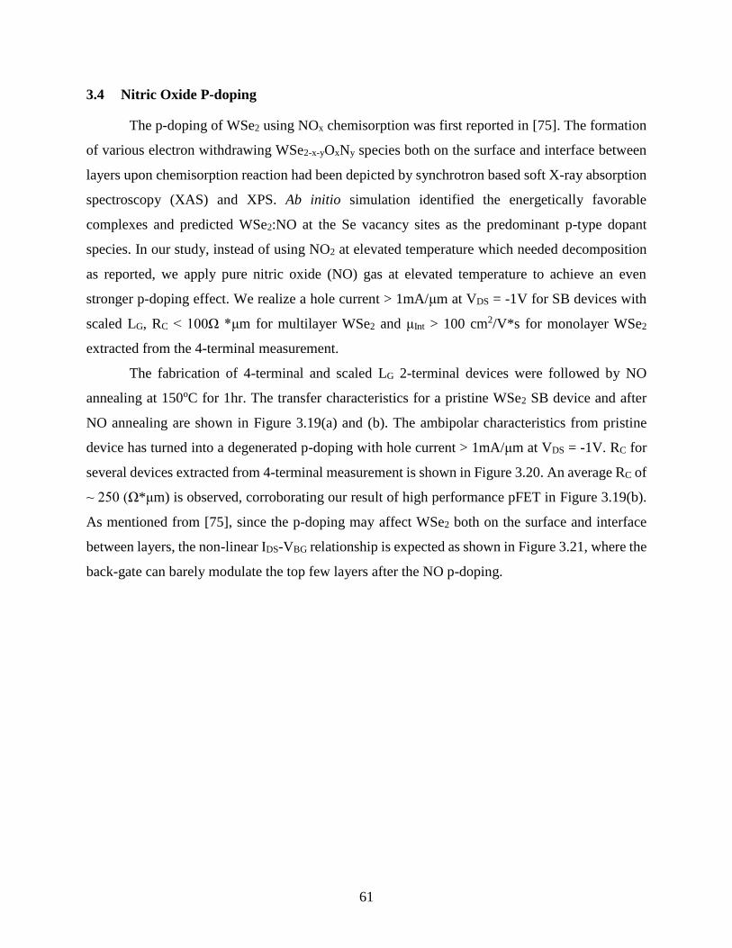
61
3.4 Nitric Oxide P-doping
The p-doping of WSe2 using NOx chemisorption was first reported in [75]. The formation
of various electron withdrawing WSe2-x-yOxNy species both on the surface and interface between
layers upon chemisorption reaction had been depicted by synchrotron based soft X-ray absorption
spectroscopy (XAS) and XPS. Ab initio simulation identified the energetically favorable
complexes and predicted WSe2:NO at the Se vacancy sites as the predominant p-type dopant
species. In our study, instead of using NO2 at elevated temperature which needed decomposition
as reported, we apply pure nitric oxide (NO) gas at elevated temperature to achieve an even
stronger p-doping effect. We realize a hole current > 1mA/μm at VDS = -1V for SB devices with
scaled LG, RC < 100Ω *μm for multilayer WSe2 and μInt > 100 cm2/V*s for monolayer WSe2
extracted from the 4-terminal measurement.
The fabrication of 4-terminal and scaled LG 2-terminal devices were followed by NO
annealing at 150oC for 1hr. The transfer characteristics for a pristine WSe2 SB device and after
NO annealing are shown in Figure 3.19(a) and (b). The ambipolar characteristics from pristine
device has turned into a degenerated p-doping with hole current > 1mA/μm at VDS = -1V. RC for
several devices extracted from 4-terminal measurement is shown in Figure 3.20. An average RC of
~ 250 (Ω*μm) is observed, corroborating our result of high performance pFET in Figure 3.19(b).
As mentioned from [75], since the p-doping may affect WSe2 both on the surface and interface
between layers, the non-linear IDS-VBG relationship is expected as shown in Figure 3.21, where the
back-gate can barely modulate the top few layers after the NO p-doping.
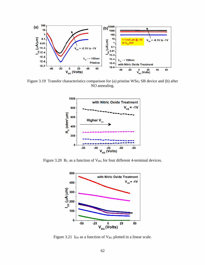
62
Figure 3.19 Transfer characteristics comparison for (a) pristine WSe2 SB device and (b) after
NO annealing.
Figure 3.20 RC as a function of VBG for four different 4-terminal devices.
Figure 3.21 IDS as a function of VBG plotted in a linear scale.
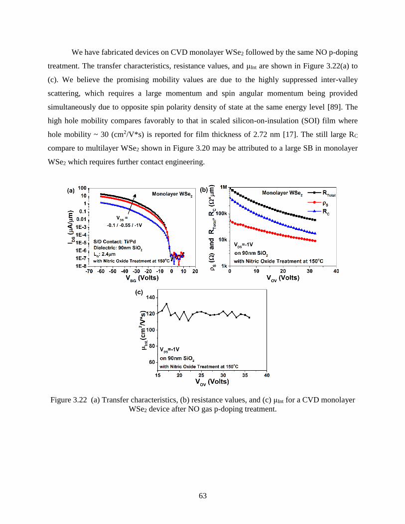
63
We have fabricated devices on CVD monolayer WSe2 followed by the same NO p-doping
treatment. The transfer characteristics, resistance values, and μInt are shown in Figure 3.22(a) to
(c). We believe the promising mobility values are due to the highly suppressed inter-valley
scattering, which requires a large momentum and spin angular momentum being provided
simultaneously due to opposite spin polarity density of state at the same energy level [89]. The
high hole mobility compares favorably to that in scaled silicon-on-insulation (SOI) film where
hole mobility ~ 30 (cm2/V*s) is reported for film thickness of 2.72 nm [17]. The still large RC
compare to multilayer WSe2 shown in Figure 3.20 may be attributed to a large SB in monolayer
WSe2 which requires further contact engineering.
Figure 3.22 (a) Transfer characteristics, (b) resistance values, and (c) μInt for a CVD monolayer
WSe2 device after NO gas p-doping treatment.
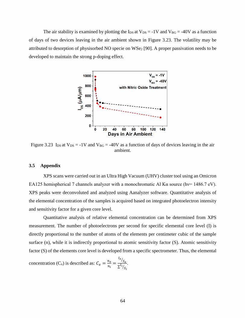
64
The air stability is examined by plotting the IDS at VDS = -1V and VBG = -40V as a function
of days of two devices leaving in the air ambient shown in Figure 3.23. The volatility may be
attributed to desorption of physisorbed NO specie on WSe2 [90]. A proper passivation needs to be
developed to maintain the strong p-doping effect.
Figure 3.23 IDS at VDS = -1V and VBG = -40V as a function of days of devices leaving in the air
ambient.
3.5 Appendix
XPS scans were carried out in an Ultra High Vacuum (UHV) cluster tool using an Omicron
EA125 hemispherical 7 channels analyzer with a monochromatic Al Kα source (hν= 1486.7 eV).
XPS peaks were deconvoluted and analyzed using Aanalyzer software. Quantitative analysis of
the elemental concentration of the samples is acquired based on integrated photoelectron intensity
and sensitivity factor for a given core level.
Quantitative analysis of relative elemental concentration can be determined from XPS
measurement. The number of photoelectrons per second for specific elemental core level (I) is
directly proportional to the number of atoms of the elements per centimeter cubic of the sample
surface (n), while it is indirectly proportional to atomic sensitivity factor (S). Atomic sensitivity
factor (S) of the elements core level is developed from a specific spectrometer. Thus, the elemental
concentration (Cx) is described as: 𝐶𝑥 =𝑛𝑥
𝑛𝑖=
𝐼𝑥𝑆𝑥
⁄
∑𝐼𝑖
𝑆𝑖⁄
.
65
3.6 Conclusion
Several doping strategies have been proposed to reduce the RC for WSe2 device. By using
fixed charge gating, the SiNx passivation brings significant n-type doping to WSe2 device,
facilitating NMOSFET and high performance SB devices (~442 μA/μm at VDS=1V)
implementation. Tunable p-type doping on WSe2 through O2-plasma treatment at different
temperatures are demonstrated, with comprehensive evidences from XPS, Raman, HRTEM and
electrical characteristics. We conclude that the doping level is determined by how many WSe2
layers being converted into WO3-x by the O2-plasma treatment. Larger number of layers are
converted at higher temperatures, resulting in thicker WO3-x for higher doping. The penetration of
WO3-x into the contact region is believed to contribute to the unpinning of the Fermi level and
thinning of the barrier width for higher current injection. Low RC ~528 *m was measured from
4-terminal measurements after 250 oC O2-plasma treatment, leading to an excellent hole current
(~320 at μA/μm at VDS= -1V) in WSe2 devices. Nitric oxide annealing on WSe2 forms various
electron withdrawing WSe2-x-yOxNy species both on the surface and interface between layers upon
chemisorption reaction, leading to a strong p-type doping effect. We realize a hole current >
1mA/μm at VDS = -1V for SB devices with scaled LG, RC < 100Ω *μm for multilayer WSe2 and
μInt > 100 cm2/V*s for monolayer WSe2 extracted from the 4-terminal measurement. While a
proper passivation is needed to maintain the strong p-doping effect.
66
ULTRA-SCALED DIELECTRIC FOR HIGH
PERFORMANCE WS2-FETS
Contents in chapter 4-2 and 4-4 has been presented in IEDM 2020 and accepted by IEEE
Transactions on Electron Devices journal (DOI: 10.1109/TED.2021.3058078). Contents in chapter
4-3 is currently submitted to 2021 VLSI Symposium.
4.1 Low Dimensional Materials as Promising Candidates for Logic Devices
As mentioned in section 1-1, 2D semiconducting transition metal dichalcogenides (TMDs)
are considered promising channel materials for ultra-scaled FET implementations to suppress
undesired short channel effects (SCEs). It is their inherent layered-structure that allows for ultimate
body thickness scaling into the sub-1nm range while preserving the desired electrostatics. Various
researchers to date have reported TMD devices with scaled channel lengths [8], [44], [91]–[97].
While some of them are able to achieve decent off-state behavior, the on-state performance is not
yet reaching the predicted values over 1 (mA/μm) [3], especially at a technological-relevant scaled
overdrive voltage (VOV = VGS-VTH, where VTH is the threshold voltage). A number of unanswered
questions and challenges are responsible for the currently off-target on-state performance. First,
Fermi-level pinning results in substantial Schottky-barrier height (SBHs) at the metal contact to
channel interface [7], [33]–[35], [98], which in turn gives rise to a large contact resistance (RC).
Since monolayer TMDs exhibit an even larger bandgap (Eg) than their multi-layer counterparts
due to more pronounced quantum confinement, even larger SBHs [42], [99], [100] and RC are
obtained in this case as will be pointed out in section 4-3. Second, it is a challenging endeavor to
deposit a scaled gate dielectric onto an inert TMD surface [101]–[103]. A rather large effective
oxide thickness (EOT) thus often prevents an efficient gate-control. Note that for most prototype
devices, contact gating is required to facilitate carrier injection. Third, prior to the work described
in this article, the impact of the TMD body thickness on the overall on-state and off-state device
performances has not been comprehensively characterized.
To address the above issues, we have performed a careful study on more than 50 multilayer
WS2 FETs and monolayer WS2 FETs to achieve a statistically relevant picture. Devices of
multilayer WS2 with body thicknesses (TCH) ranging from 2.1nm (~3 layers) to 7nm (~10 layers)
and channel lengths (LG) ranging from 40nm to 400nm were evaluated. Devices were all
67
implemented on 2.8nm HfO2 with an EOT of less than 1nm. Ideal off-state behavior was observed,
including near ideal subthreshold slopes (SS), a tight VTH distribution, and small drain-induced
barrier lowering (DIBL) given a proper selection of TCH. A record high on-state current and ultra-
low RC values were observed for FETs with TCH = 2.1nm at scaled VOV, achieving ~ 350 (μA/μm)
at VDS =VOV =1V and > 600 (μA/μm) at VOV =2V in a double-gated structure. We attribute the
achieved high performance to the utilization of ultra-scaled gate dielectrics and small channel body
thickness. For devices based on monolayer WS2, the best ION ~ 180 (μA/μm) at VDS =VOV =1V
and ION ~ 320 (μA/μm) at VOV =2V in a double-gated structure were achieved. A higher RC for
monolayer WS2 comparing to “thin” multilayer WS2 is attributed to a larger SBH associated with
metal-semiconductor interfaces.
To understand the impact of TCH on the on-state performance, a detailed discussion on a
unique gating effect in 2D TMD FETs that involves the region underneath the source/drain metal
contacts is presented [104]. Based on technology computer aided design (TCAD) simulations, we
conclude that the back-gating efficiency for thick body devices is lower than for thin ones, resulting
in a larger effective tunneling distance for carrier injection from the metal contact into the channel.
However, as mentioned above, the lower on-state performance for monolayer WS2 FETs implies
in particular that monolayer TMD devices are expected to receive the strongest contact gating and
good injection into the channel, but the device on-state may suffer from too large RC-values
associated with a large SBH at the contact interface as mentioned above [99], [100]. Therefore,
further studies on the topics of reliable doping schemes [41], [66], [73], [105], [106], phase change
contacts [9], [107], and contact Fermi-level de-pinning [52], [77], [108] are urgently required to
facilitate the integration of 2D TMD-based CMOS for a beyond-Si era.
4.2 Multilayer WS2 FETs
4.2.1 Ultra-scale Dielectric WS2-FETs
As shown in the process flow displayed in Figure 4.1(a), a gate-first process was employed
by patterning a local bottom gate (BG) from a Ti (3nm) / Au (7nm) stack followed by ~2.8nm
HfO2 deposition using ALD at 90oC serving as the gate dielectric. WS2 flakes were mechanically
exfoliated onto the bottom gates, followed by e-beam lithography to define Ni source/drain (S/D)
contacts and FET channels with LG ranging from 40nm to 400nm. WS2 flakes with TCH varying
68
from 2.1nm to 7nm were identified by utilizing an atomic force microscope (AFM). For devices
that went through a subsequent top gate (TG) fabrication process, 1.2nm Al was first deposited as
a seeding layer which turned into ~ 2.5nm Al2O3 as evident from the transmission electron
microscope (TEM) image shown in Figure 4.1(b), followed by ~5.5nm ALD HfO2 deposition. A
Ni gate electrode was then defined on top of these devices to complete the double gate device
structure. All metals were e-beam evaporated under chamber pressure ~ 5*10-7 torr. Devices were
annealed in vacuum at 385K for 6 hours (before top gate implementation) to reduce moisture and
trap charges. A scanning electron microscope (SEM) image of a set of devices with various LG is
shown in Figure 4.1(c). The TEM image shown in Figure 4.1(b) reveals that 3 layers of WS2 are
forming this particular FET channel sitting conformally on the 2.8nm HfO2 bottom gate dielectric.
Having both the body thickness and the gate dielectric being scaled is the key to simultaneously
achieve good off-state and excellent on-state performance at scaled VOV, as discussed in the
following.
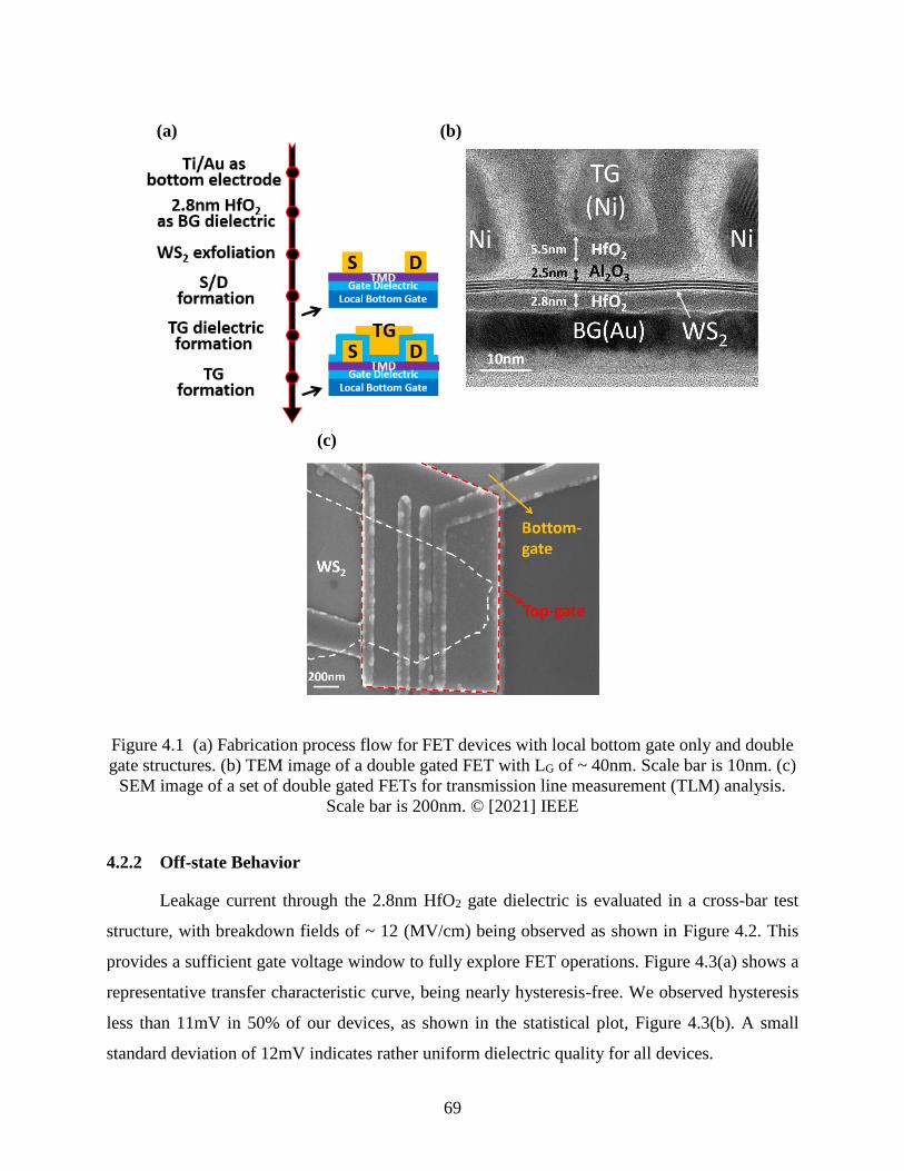
69
Figure 4.1 (a) Fabrication process flow for FET devices with local bottom gate only and double
gate structures. (b) TEM image of a double gated FET with LG of ~ 40nm. Scale bar is 10nm. (c)
SEM image of a set of double gated FETs for transmission line measurement (TLM) analysis.
Scale bar is 200nm. © [2021] IEEE
4.2.2 Off-state Behavior
Leakage current through the 2.8nm HfO2 gate dielectric is evaluated in a cross-bar test
structure, with breakdown fields of ~ 12 (MV/cm) being observed as shown in Figure 4.2. This
provides a sufficient gate voltage window to fully explore FET operations. Figure 4.3(a) shows a
representative transfer characteristic curve, being nearly hysteresis-free. We observed hysteresis
less than 11mV in 50% of our devices, as shown in the statistical plot, Figure 4.3(b). A small
standard deviation of 12mV indicates rather uniform dielectric quality for all devices.
(a) (b)
(c)
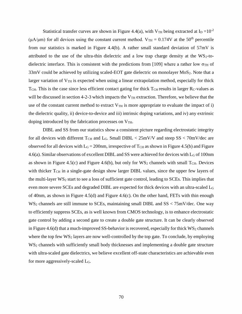
70
Statistical transfer curves are shown in Figure 4.4(a), with VTH being extracted at ID =10-2
(μA/μm) for all devices using the constant current method. VTH = 0.174V at the 50th percentile
from our statistics is marked in Figure 4.4(b). A rather small standard deviation of 57mV is
attributed to the use of the ultra-thin dielectric and a low trap charge density at the WS2-to-
dielectric interface. This is consistent with the predictions from [109] where a rather low σTH of
33mV could be achieved by utilizing scaled-EOT gate dielectric on monolayer MoS2. Note that a
larger variation of VTH is expected when using a linear extrapolation method, especially for thick
TCH. This is the case since less efficient contact gating for thick TCH results in larger RC-values as
will be discussed in section 4-2-3 which impacts the VTH extraction. Therefore, we believe that the
use of the constant current method to extract VTH is more appropriate to evaluate the impact of i)
the dielectric quality, ii) device-to-device and iii) intrinsic doping variations, and iv) any extrinsic
doping introduced by the fabrication processes on VTH.
DIBL and SS from our statistics show a consistent picture regarding electrostatic integrity
for all devices with different TCH and LG. Small DIBL < 25mV/V and steep SS < 70mV/dec are
observed for all devices with LG = 200nm, irrespective of TCH as shown in Figure 4.5(b) and Figure
4.6(a). Similar observations of excellent DIBL and SS were achieved for devices with LG of 100nm
as shown in Figure 4.5(c) and Figure 4.6(b), but only for WS2 channels with small TCH. Devices
with thicker TCH in a single-gate design show larger DIBL values, since the upper few layers of
the multi-layer WS2 start to see a loss of sufficient gate control, leading to SCEs. This implies that
even more severe SCEs and degraded DIBL are expected for thick devices with an ultra-scaled LG
of 40nm, as shown in Figure 4.5(d) and Figure 4.6(c). On the other hand, FETs with thin enough
WS2 channels are still immune to SCEs, maintaining small DIBL and SS < 75mV/dec. One way
to efficiently suppress SCEs, as is well known from CMOS technology, is to enhance electrostatic
gate control by adding a second gate to create a double gate structure. It can be clearly observed
in Figure 4.6(d) that a much-improved SS-behavior is recovered, especially for thick WS2 channels
where the top few WS2 layers are now well-controlled by the top gate. To conclude, by employing
WS2 channels with sufficiently small body thicknesses and implementing a double gate structure
with ultra-scaled gate dielectrics, we believe excellent off-state characteristics are achievable even
for more aggressively-scaled LG.
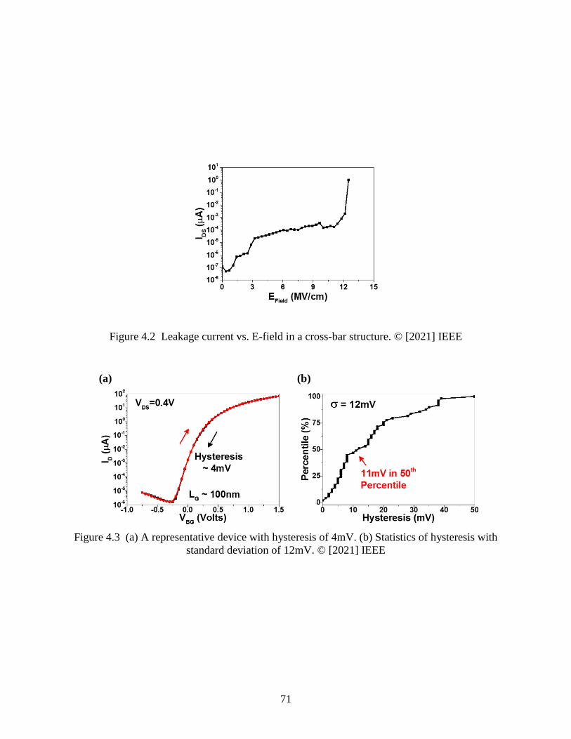
71
Figure 4.2 Leakage current vs. E-field in a cross-bar structure. © [2021] IEEE
Figure 4.3 (a) A representative device with hysteresis of 4mV. (b) Statistics of hysteresis with
standard deviation of 12mV. © [2021] IEEE
(a) (b)
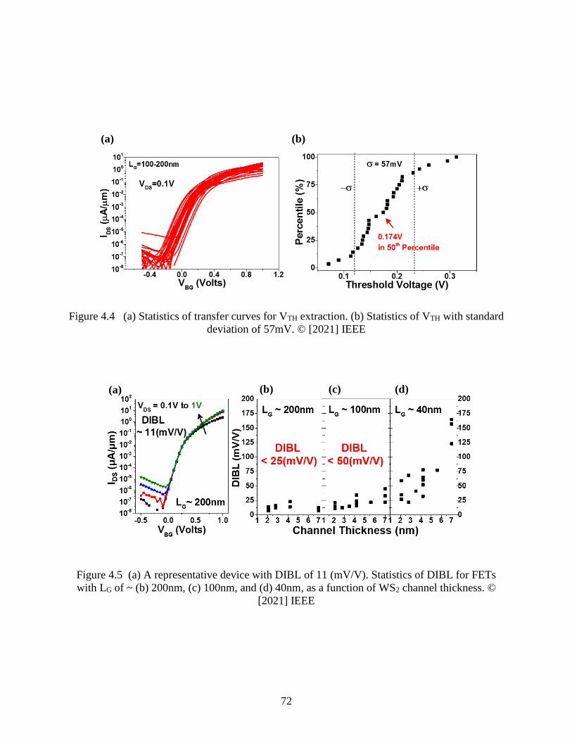
72
Figure 4.4 (a) Statistics of transfer curves for VTH extraction. (b) Statistics of VTH with standard
deviation of 57mV. © [2021] IEEE
Figure 4.5 (a) A representative device with DIBL of 11 (mV/V). Statistics of DIBL for FETs
with LG of ~ (b) 200nm, (c) 100nm, and (d) 40nm, as a function of WS2 channel thickness. ©
[2021] IEEE
(a) (b)
(a) (b) (c) (d)
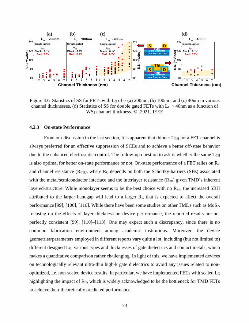
73
Figure 4.6 Statistics of SS for FETs with LG of ~ (a) 200nm, (b) 100nm, and (c) 40nm in various
channel thicknesses. (d) Statistics of SS for double gated FETs with LG ~ 40nm as a function of
WS2 channel thickness. © [2021] IEEE
4.2.3 On-state Performance
From our discussion in the last section, it is apparent that thinner TCH for a FET channel is
always preferred for an effective suppression of SCEs and to achieve a better off-state behavior
due to the enhanced electrostatic control. The follow-up question to ask is whether the same TCH
is also optimal for better on-state performance or not. On-state performance of a FET relies on RC
and channel resistance (RCH), where RC depends on both the Schottky-barriers (SBs) associated
with the metal/semiconductor interface and the interlayer resistance (Rint) given TMD’s inherent
layered-structure. While monolayer seems to be the best choice with no Rint, the increased SBH
attributed to the larger bandgap will lead to a larger RC that is expected to affect the overall
performance [99], [100], [110]. While there have been some studies on other TMDs such as MoS2,
focusing on the effects of layer thickness on device performance, the reported results are not
perfectly consistent [99], [110]–[113]. One may expect such a discrepancy, since there is no
common fabrication environment among academic institutions. Moreover, the device
geometries/parameters employed in different reports vary quite a lot, including (but not limited to)
different designed LG, various types and thicknesses of gate dielectrics and contact metals, which
makes a quantitative comparison rather challenging. In light of this, we have implemented devices
on technologically relevant ultra-thin high-k gate dielectrics to avoid any issues related to non-
optimized, i.e. non-scaled device results. In particular, we have implemented FETs with scaled LG
highlighting the impact of RC, which is widely acknowledged to be the bottleneck for TMD FETs
to achieve their theoretically predicted performance.
(a) (b) (c) (d)
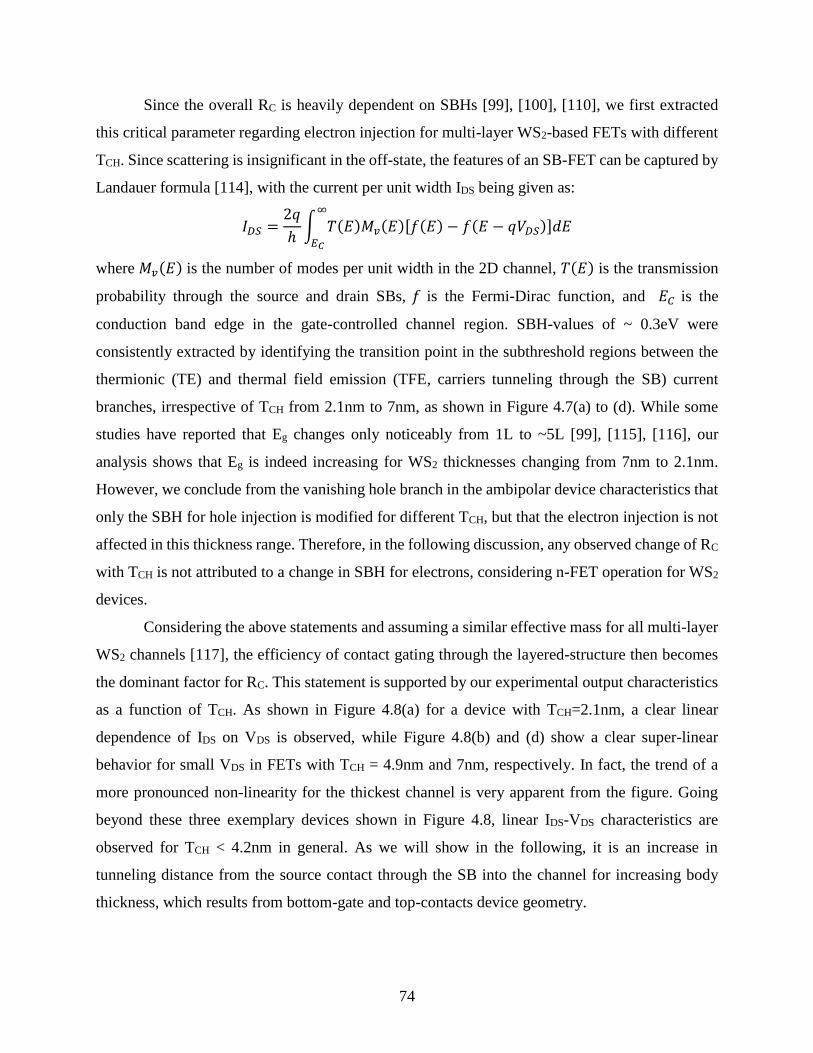
74
Since the overall RC is heavily dependent on SBHs [99], [100], [110], we first extracted
this critical parameter regarding electron injection for multi-layer WS2-based FETs with different
TCH. Since scattering is insignificant in the off-state, the features of an SB-FET can be captured by
Landauer formula [114], with the current per unit width IDS being given as:
𝐼𝐷𝑆 =2𝑞
ℎ∫ 𝑇(𝐸)𝑀𝑣(𝐸)[𝑓(𝐸) − 𝑓(𝐸 − 𝑞𝑉𝐷𝑆)]𝑑𝐸
∞
𝐸𝐶
where 𝑀𝑣(𝐸) is the number of modes per unit width in the 2D channel, 𝑇(𝐸) is the transmission
probability through the source and drain SBs, 𝑓 is the Fermi-Dirac function, and 𝐸𝐶 is the
conduction band edge in the gate-controlled channel region. SBH-values of ~ 0.3eV were
consistently extracted by identifying the transition point in the subthreshold regions between the
thermionic (TE) and thermal field emission (TFE, carriers tunneling through the SB) current
branches, irrespective of TCH from 2.1nm to 7nm, as shown in Figure 4.7(a) to (d). While some
studies have reported that Eg changes only noticeably from 1L to ~5L [99], [115], [116], our
analysis shows that Eg is indeed increasing for WS2 thicknesses changing from 7nm to 2.1nm.
However, we conclude from the vanishing hole branch in the ambipolar device characteristics that
only the SBH for hole injection is modified for different TCH, but that the electron injection is not
affected in this thickness range. Therefore, in the following discussion, any observed change of RC
with TCH is not attributed to a change in SBH for electrons, considering n-FET operation for WS2
devices.
Considering the above statements and assuming a similar effective mass for all multi-layer
WS2 channels [117], the efficiency of contact gating through the layered-structure then becomes
the dominant factor for RC. This statement is supported by our experimental output characteristics
as a function of TCH. As shown in Figure 4.8(a) for a device with TCH=2.1nm, a clear linear
dependence of IDS on VDS is observed, while Figure 4.8(b) and (d) show a clear super-linear
behavior for small VDS in FETs with TCH = 4.9nm and 7nm, respectively. In fact, the trend of a
more pronounced non-linearity for the thickest channel is very apparent from the figure. Going
beyond these three exemplary devices shown in Figure 4.8, linear IDS-VDS characteristics are
observed for TCH < 4.2nm in general. As we will show in the following, it is an increase in
tunneling distance from the source contact through the SB into the channel for increasing body
thickness, which results from bottom-gate and top-contacts device geometry.
75
To elucidate this point, we have performed TCAD simulations using Sentaurus Device to
analyze the carrier distribution in single-gated WS2 channels with different TCH. As shown in
Figure 4.9(a), when a large VOV=1.4V is applied, the accumulated electrons are mainly located at
the bottom of the WS2 channel in the bottom-gate device structure. Therefore, the carrier injection
from the source contact in a device with larger TCH inevitably requires a larger tunneling distance
λ to reach the accumulation channel and contribute to current conduction, which leads to a larger
contact resistance RC. In turn, in a device with larger TCH, the increase in quasi Fermi level drop
ΔEF,n across the source contact will become larger when VDS increases, as shown in the band
diagram in Figure 4.9(b), which leads to the super-linear current increase as revealed in Figure
4.8(d), while is not the case for thin TCH as shown in Figure 4.8(a) and Figure 4.9(b). In addition,
it is interesting to observe that the non-linearity is somehow “vanishing” for the device with LG =
400nm in Figure 4.8(c), which agrees with our analysis that in a long channel device due to the
channel resistance being much larger than RC, the impact of increasing VDS on the quasi Fermi
level drop across the contact ΔEF,n becomes less prominent. Therefore, it is always critical to
investigate devices with short LG in order to reveal any possible effects in the contact regions.
76
Figure 4.7 Transfer curves fitting from Landauer formula for devices with TCH of (a) 2.1nm, (b)
2.8nm, (c) 4.9nm, and (d) 7.0nm.
(a) (b)
(c) (d)
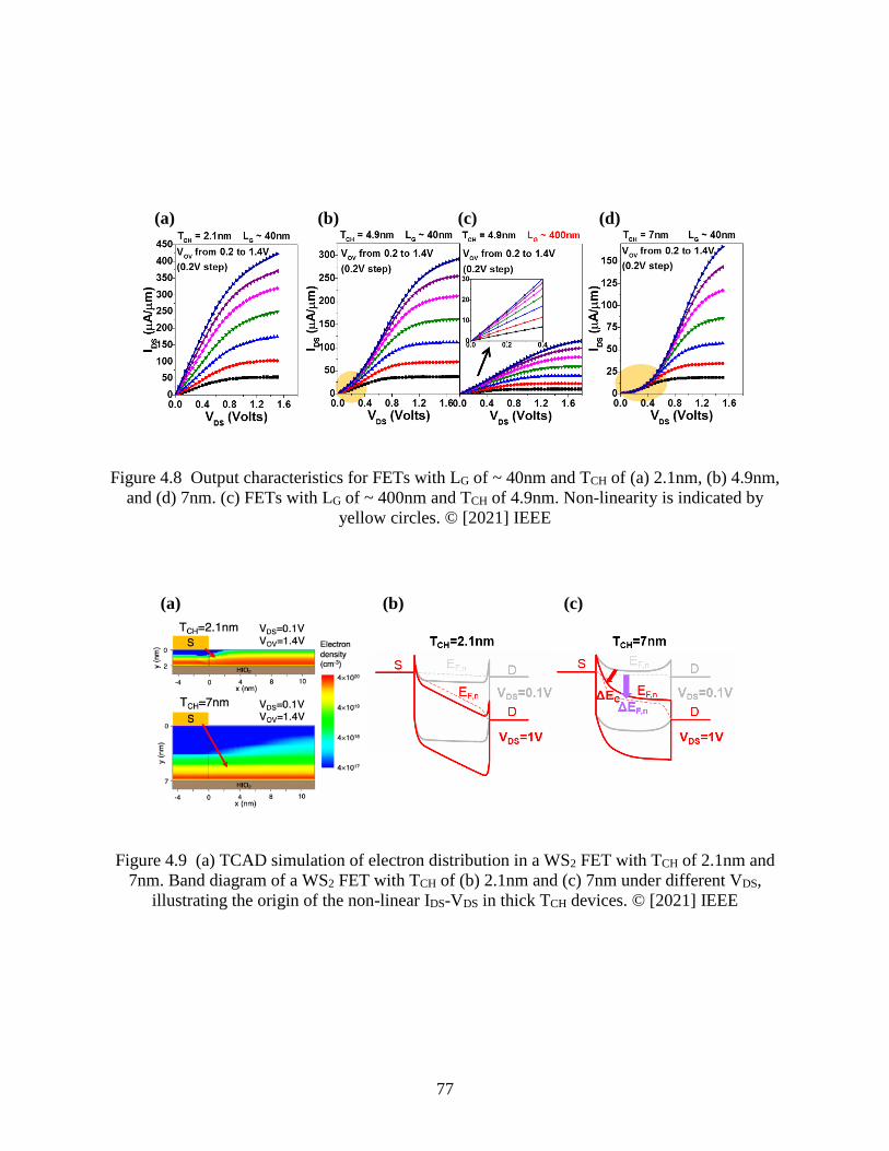
77
Figure 4.8 Output characteristics for FETs with LG of ~ 40nm and TCH of (a) 2.1nm, (b) 4.9nm,
and (d) 7nm. (c) FETs with LG of ~ 400nm and TCH of 4.9nm. Non-linearity is indicated by
yellow circles. © [2021] IEEE
Figure 4.9 (a) TCAD simulation of electron distribution in a WS2 FET with TCH of 2.1nm and
7nm. Band diagram of a WS2 FET with TCH of (b) 2.1nm and (c) 7nm under different VDS,
illustrating the origin of the non-linear IDS-VDS in thick TCH devices. © [2021] IEEE
(a) (b) (c) (d)
(a) (b) (c)
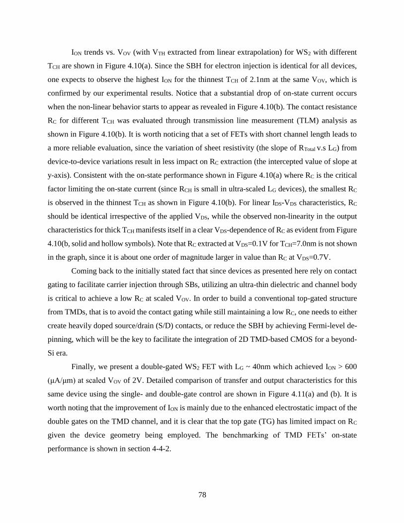
78
ION trends vs. VOV (with VTH extracted from linear extrapolation) for WS2 with different
TCH are shown in Figure 4.10(a). Since the SBH for electron injection is identical for all devices,
one expects to observe the highest ION for the thinnest TCH of 2.1nm at the same VOV, which is
confirmed by our experimental results. Notice that a substantial drop of on-state current occurs
when the non-linear behavior starts to appear as revealed in Figure 4.10(b). The contact resistance
RC for different TCH was evaluated through transmission line measurement (TLM) analysis as
shown in Figure 4.10(b). It is worth noticing that a set of FETs with short channel length leads to
a more reliable evaluation, since the variation of sheet resistivity (the slope of RTotal v.s LG) from
device-to-device variations result in less impact on RC extraction (the intercepted value of slope at
y-axis). Consistent with the on-state performance shown in Figure 4.10(a) where RC is the critical
factor limiting the on-state current (since RCH is small in ultra-scaled LG devices), the smallest RC
is observed in the thinnest TCH as shown in Figure 4.10(b). For linear IDS-VDS characteristics, RC
should be identical irrespective of the applied VDS, while the observed non-linearity in the output
characteristics for thick TCH manifests itself in a clear VDS-dependence of RC as evident from Figure
4.10(b, solid and hollow symbols). Note that RC extracted at VDS=0.1V for TCH=7.0nm is not shown
in the graph, since it is about one order of magnitude larger in value than RC at VDS=0.7V.
Coming back to the initially stated fact that since devices as presented here rely on contact
gating to facilitate carrier injection through SBs, utilizing an ultra-thin dielectric and channel body
is critical to achieve a low RC at scaled VOV. In order to build a conventional top-gated structure
from TMDs, that is to avoid the contact gating while still maintaining a low RC, one needs to either
create heavily doped source/drain (S/D) contacts, or reduce the SBH by achieving Fermi-level de-
pinning, which will be the key to facilitate the integration of 2D TMD-based CMOS for a beyond-
Si era.
Finally, we present a double-gated WS2 FET with LG ~ 40nm which achieved ION > 600
(μA/μm) at scaled VOV of 2V. Detailed comparison of transfer and output characteristics for this
same device using the single- and double-gate control are shown in Figure 4.11(a) and (b). It is
worth noting that the improvement of ION is mainly due to the enhanced electrostatic impact of the
double gates on the TMD channel, and it is clear that the top gate (TG) has limited impact on RC
given the device geometry being employed. The benchmarking of TMD FETs’ on-state
performance is shown in section 4-4-2.
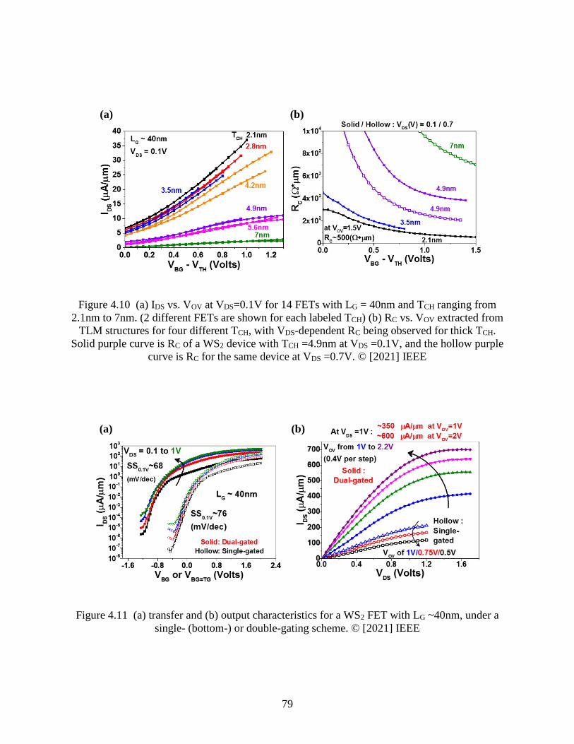
79
Figure 4.10 (a) IDS vs. VOV at VDS=0.1V for 14 FETs with LG = 40nm and TCH ranging from
2.1nm to 7nm. (2 different FETs are shown for each labeled TCH) (b) RC vs. VOV extracted from
TLM structures for four different TCH, with VDS-dependent RC being observed for thick TCH.
Solid purple curve is RC of a WS2 device with TCH =4.9nm at VDS =0.1V, and the hollow purple
curve is RC for the same device at VDS =0.7V. © [2021] IEEE
Figure 4.11 (a) transfer and (b) output characteristics for a WS2 FET with LG ~40nm, under a
single- (bottom-) or double-gating scheme. © [2021] IEEE
(a) (b)
(a) (b)
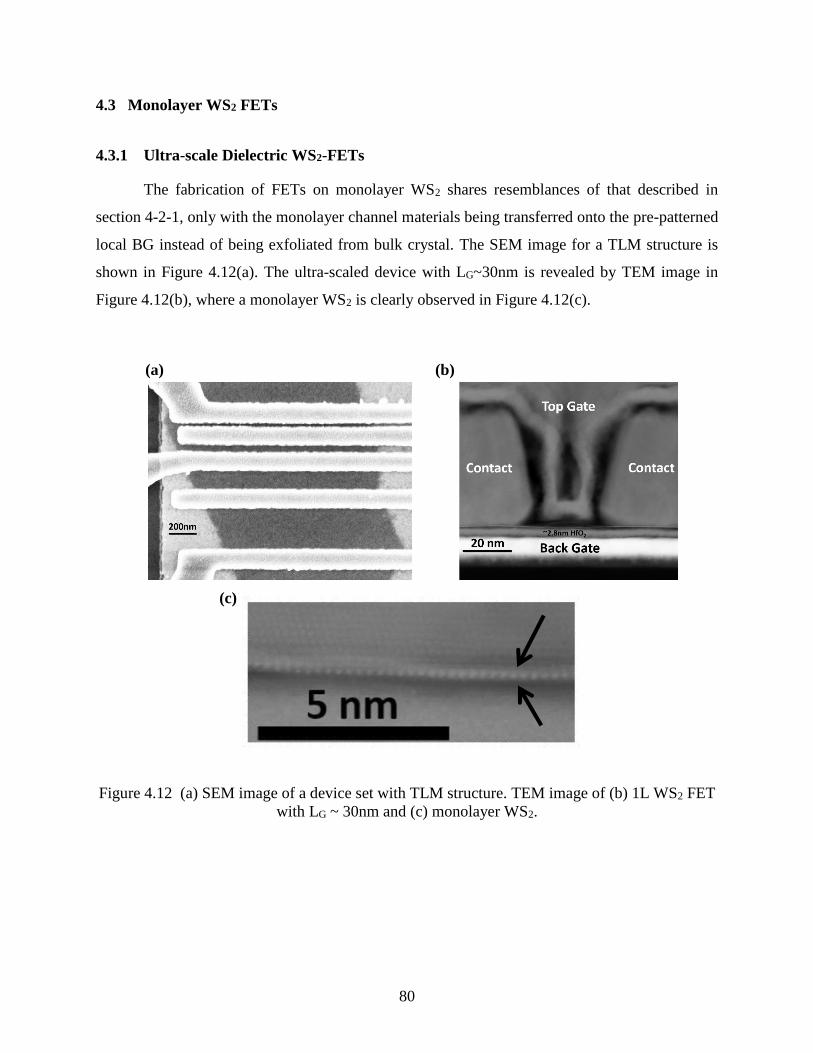
80
4.3 Monolayer WS2 FETs
4.3.1 Ultra-scale Dielectric WS2-FETs
The fabrication of FETs on monolayer WS2 shares resemblances of that described in
section 4-2-1, only with the monolayer channel materials being transferred onto the pre-patterned
local BG instead of being exfoliated from bulk crystal. The SEM image for a TLM structure is
shown in Figure 4.12(a). The ultra-scaled device with LG~30nm is revealed by TEM image in
Figure 4.12(b), where a monolayer WS2 is clearly observed in Figure 4.12(c).
Figure 4.12 (a) SEM image of a device set with TLM structure. TEM image of (b) 1L WS2 FET
with LG ~ 30nm and (c) monolayer WS2.
(a) (b)
(c)
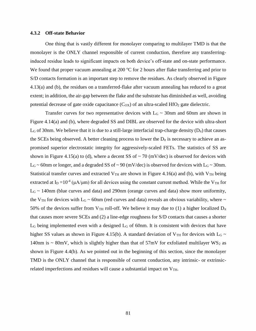
81
4.3.2 Off-state Behavior
One thing that is vastly different for monolayer comparing to multilayer TMD is that the
monolayer is the ONLY channel responsible of current conduction, therefore any transferring-
induced residue leads to significant impacts on both device’s off-state and on-state performance.
We found that proper vacuum annealing at 200 oC for 2 hours after flake transferring and prior to
S/D contacts formation is an important step to remove the residues. As clearly observed in Figure
4.13(a) and (b), the residues on a transferred-flake after vacuum annealing has reduced to a great
extent; in addition, the air-gap between the flake and the substrate has diminished as well, avoiding
potential decrease of gate oxide capacitance (COX) of an ultra-scaled HfO2 gate dielectric.
Transfer curves for two representative devices with LG ~ 30nm and 60nm are shown in
Figure 4.14(a) and (b), where degraded SS and DIBL are observed for the device with ultra-short
LG of 30nm. We believe that it is due to a still-large interfacial trap-charge density (Dit) that causes
the SCEs being observed. A better cleaning process to lower the Dit is necessary to achieve an as-
promised superior electrostatic integrity for aggressively-scaled FETs. The statistics of SS are
shown in Figure 4.15(a) to (d), where a decent SS of ~ 70 (mV/dec) is observed for devices with
LG ~ 60nm or longer, and a degraded SS of ~ 90 (mV/dec) is observed for devices with LG ~ 30nm.
Statistical transfer curves and extracted VTH are shown in Figure 4.16(a) and (b), with VTH being
extracted at ID =10-4 (μA/μm) for all devices using the constant current method. While the VTH for
LG ~ 140nm (blue curves and data) and 290nm (orange curves and data) show more uniformity,
the VTH for devices with LG ~ 60nm (red curves and data) reveals an obvious variability, where ~
50% of the devices suffer from VTH roll-off. We believe it may due to (1) a higher localized Dit
that causes more severe SCEs and (2) a line-edge roughness for S/D contacts that causes a shorter
LG being implemented even with a designed LG of 60nm. It is consistent with devices that have
higher SS values as shown in Figure 4.15(b). A standard deviation of VTH for devices with LG ~
140nm is ~ 80mV, which is slightly higher than that of 57mV for exfoliated multilayer WS2 as
shown in Figure 4.4(b). As we pointed out in the beginning of this section, since the monolayer
TMD is the ONLY channel that is responsible of current conduction, any intrinsic- or extrinsic-
related imperfections and residues will cause a substantial impact on VTH.
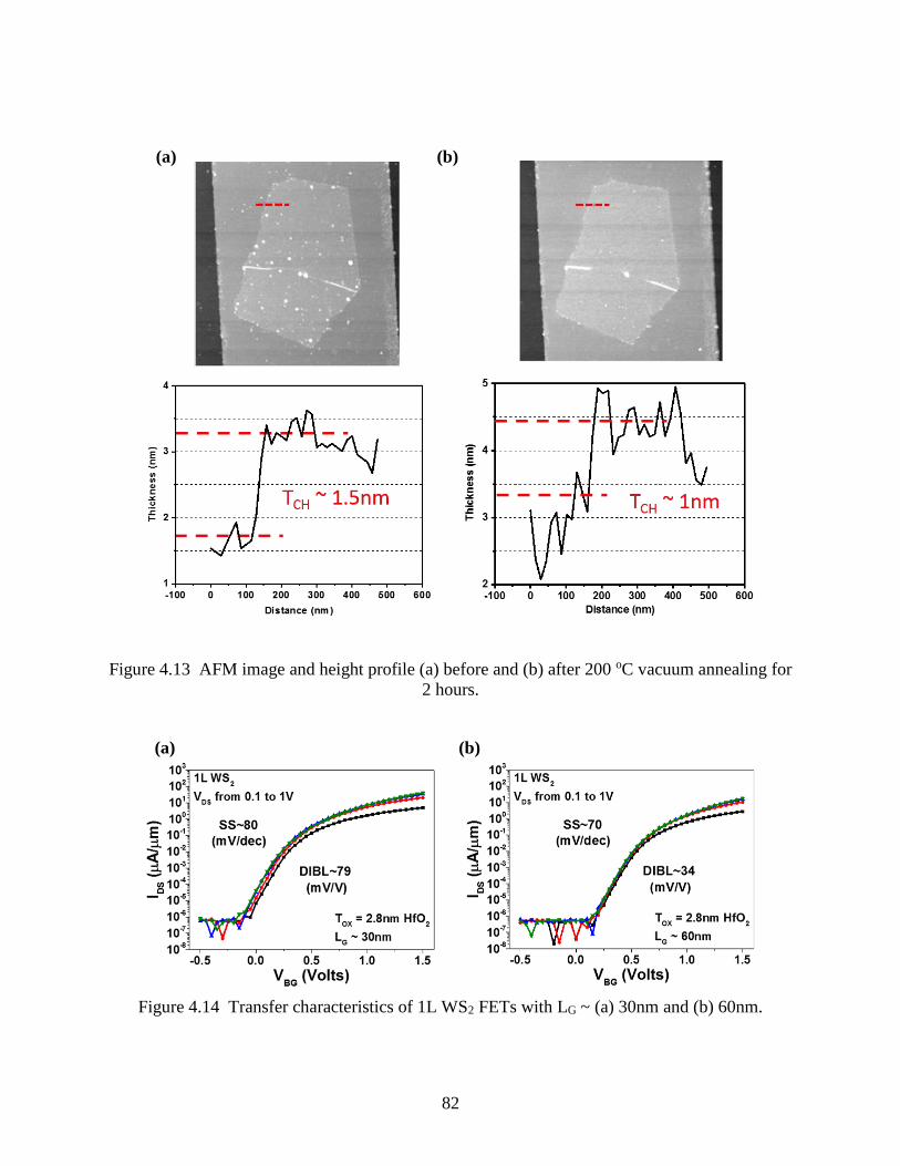
82
Figure 4.13 AFM image and height profile (a) before and (b) after 200 oC vacuum annealing for
2 hours.
Figure 4.14 Transfer characteristics of 1L WS2 FETs with LG ~ (a) 30nm and (b) 60nm.
(a) (b)
(b) (a)
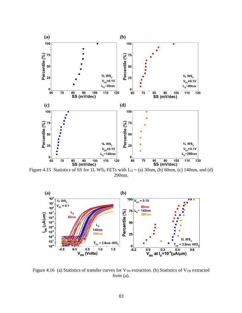
83
Figure 4.15 Statistics of SS for 1L WS2 FETs with LG ~ (a) 30nm, (b) 60nm, (c) 140nm, and (d)
290nm.
Figure 4.16 (a) Statistics of transfer curves for VTH extraction. (b) Statistics of VTH extracted
from (a).
(a) (b)
(c) (d)
(a) (b)
84
4.3.3 On-state Performance
From section 4-2-3, we concluded that for SB devices with a typical BG geometry, a
channel with thinner TCH will receive a more efficient contact gating, resulting in a lower RC at a
same given VOV as shown in Figure 4.10(b). Following the same logic, we should expect an even
lower RC being achieved for monolayer WS2. However, due to a most pronounced quantum
confinement for monolayer TMDs, a larger SBHs [42], [99], [100] will be obtained, leading to a
higher RC being observed. A larger SBHs for monolayer ~ 0.4eV is corroborated by fitting six 1L
WS2 FETs from Landauer formula as shown in Figure 4.17. Figure 4.18 shows statistical RC vs
VOV for devices with 1L WS2 channel in comparison with that for devices with multilayer WS2
channel as shown in Figure 4.10(b). A higher RC is clearly observed for monolayer WS2 (red curves)
comparing to “thin” multilayer counterparts. However, it is noted that the air-gap between the
dielectric and monolayer WS2 as revealed in Figure 4.13 may potentially lead to lower COX,
resulting in an unnecessarily large VOV being needed in order to achieve a low RC. For double-
gated structure, similar to the multilayer devices as mentioned in section 4-2-3, the TG has limited
impact on RC given the device geometry being employed. The RC vs VOV for single- and double-
gated 1L WS2 devices is shown in Figure 4.19, where a TG cannot further reduce the RC under the
same VOV. Therefore, as shown in Figure 4.20(a) to (d), it is expected that the improvement of on-
state performance will be more significant for long channel devices comparing to short channel
ones, where the device’s total resistance (RTotal) is primarily dominant by RC. The output
characteristics are shown in Figure 4.21(a) and (b) for double-gated 1L WS2 FETs with LG ~ 30nm
and 290nm. Different from that shown in Figure 4.8(b) and (d), we believe a slight non-linear
behavior revealed in Figure 4.21(a) is due to a prominent drain barrier at small VDS which is
attributed to a larger SBH for monolayer WS2, instead of having an inefficient contact gating for
thick channels. On the other hand, the Figure 4.21(b) shares similarity to Figure 4.8(c) that an
appeared “vanishing” non-linearity is due to the channel resistance being much larger than RC in
a long channel devices. Therefore, we cannot further emphasize the importance to investigate
devices with short LG in order to reveal any possible effects in the contact regions.
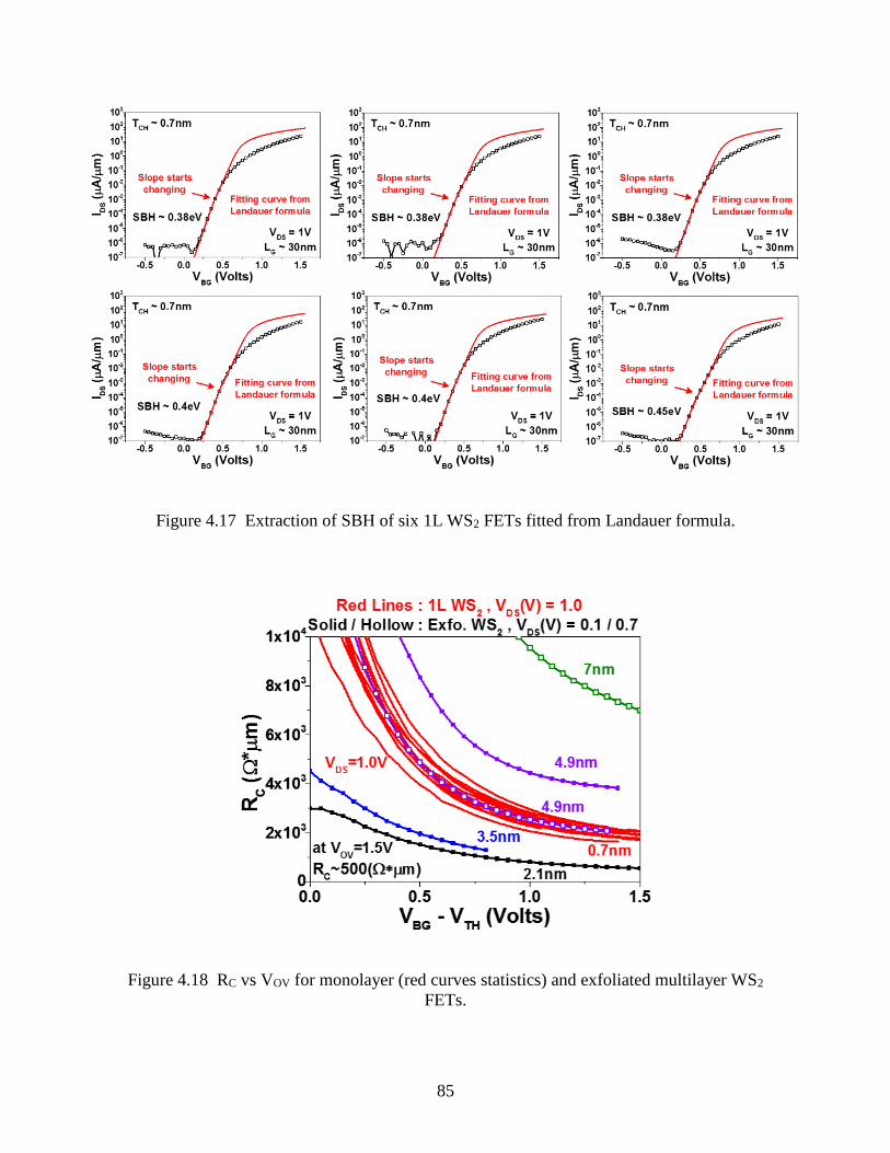
85
Figure 4.17 Extraction of SBH of six 1L WS2 FETs fitted from Landauer formula.
Figure 4.18 RC vs VOV for monolayer (red curves statistics) and exfoliated multilayer WS2
FETs.
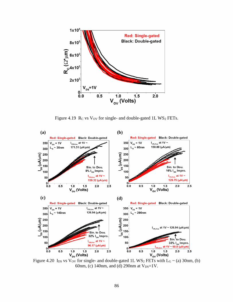
86
Figure 4.19 RC vs VOV for single- and double-gated 1L WS2 FETs.
Figure 4.20 IDS vs VOV for single- and double-gated 1L WS2 FETs with LG ~ (a) 30nm, (b)
60nm, (c) 140nm, and (d) 290nm at VDS=1V.
(b) (a)
(c) (d)
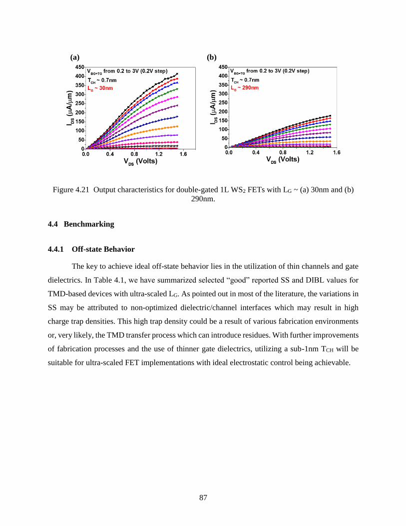
87
Figure 4.21 Output characteristics for double-gated 1L WS2 FETs with LG ~ (a) 30nm and (b)
290nm.
4.4 Benchmarking
4.4.1 Off-state Behavior
The key to achieve ideal off-state behavior lies in the utilization of thin channels and gate
dielectrics. In Table 4.1, we have summarized selected “good” reported SS and DIBL values for
TMD-based devices with ultra-scaled LG. As pointed out in most of the literature, the variations in
SS may be attributed to non-optimized dielectric/channel interfaces which may result in high
charge trap densities. This high trap density could be a result of various fabrication environments
or, very likely, the TMD transfer process which can introduce residues. With further improvements
of fabrication processes and the use of thinner gate dielectrics, utilizing a sub-1nm TCH will be
suitable for ultra-scaled FET implementations with ideal electrostatic control being achievable.
(a) (b)
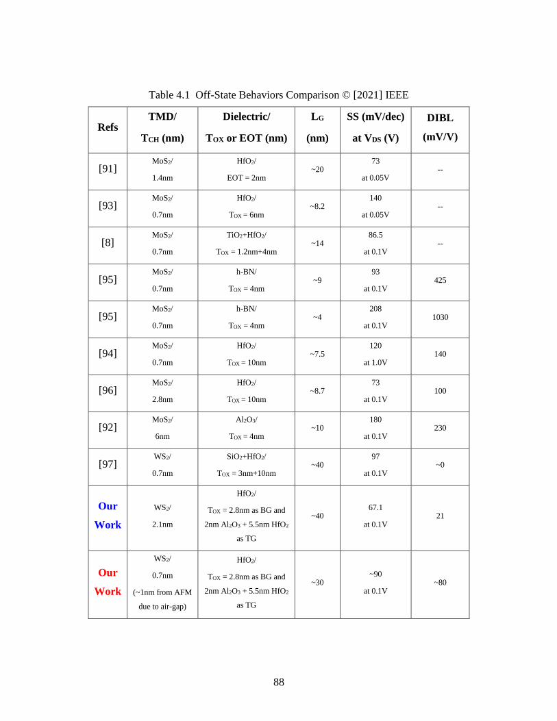
88
Table 4.1 Off-State Behaviors Comparison © [2021] IEEE
Refs TMD/
TCH (nm)
Dielectric/
TOX or EOT (nm)
LG
(nm)
SS (mV/dec)
at VDS (V)
DIBL
(mV/V)
[91] MoS2/
1.4nm
HfO2/
EOT = 2nm ~20
73
at 0.05V --
[93] MoS2/
0.7nm
HfO2/
TOX = 6nm ~8.2
140
at 0.05V --
[8] MoS2/
0.7nm
TiO2+HfO2/
TOX = 1.2nm+4nm ~14
86.5
at 0.1V --
[95] MoS2/
0.7nm
h-BN/
TOX = 4nm ~9
93
at 0.1V 425
[95] MoS2/
0.7nm
h-BN/
TOX = 4nm ~4
208
at 0.1V 1030
[94] MoS2/
0.7nm
HfO2/
TOX = 10nm ~7.5
120
at 1.0V 140
[96] MoS2/
2.8nm
HfO2/
TOX = 10nm ~8.7
73
at 0.1V 100
[92] MoS2/
6nm
Al2O3/
TOX = 4nm ~10
180
at 0.1V 230
[97] WS2/
0.7nm
SiO2+HfO2/
TOX = 3nm+10nm ~40
97
at 0.1V ~0
Our
Work
WS2/
2.1nm
HfO2/
TOX = 2.8nm as BG and
2nm Al2O3 + 5.5nm HfO2
as TG
~40 67.1
at 0.1V 21
Our
Work
WS2/
0.7nm
(~1nm from AFM
due to air-gap)
HfO2/
TOX = 2.8nm as BG and
2nm Al2O3 + 5.5nm HfO2
as TG
~30 ~90
at 0.1V ~80
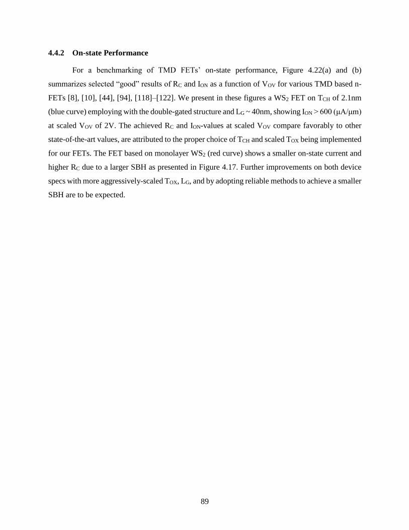
89
4.4.2 On-state Performance
For a benchmarking of TMD FETs’ on-state performance, Figure 4.22(a) and (b)
summarizes selected “good” results of RC and ION as a function of VOV for various TMD based n-
FETs [8], [10], [44], [94], [118]–[122]. We present in these figures a WS2 FET on TCH of 2.1nm
(blue curve) employing with the double-gated structure and LG ~ 40nm, showing ION > 600 (μA/μm)
at scaled VOV of 2V. The achieved RC and ION-values at scaled VOV compare favorably to other
state-of-the-art values, are attributed to the proper choice of TCH and scaled TOX being implemented
for our FETs. The FET based on monolayer WS2 (red curve) shows a smaller on-state current and
higher RC due to a larger SBH as presented in Figure 4.17. Further improvements on both device
specs with more aggressively-scaled TOX, LG, and by adopting reliable methods to achieve a smaller
SBH are to be expected.
90
Figure 4.22 Benchmarking of (a) RC and (b) ION vs VOV, with devices’ parameters listed below:
(For (b), VDS=1V unless specified) (Device parameters/geometries of each reference are shown
in next page). © [2021] IEEE
(b)
(a)
91
References for Figure 4.21(a):
[Ref #]: Layer # TMD, Dielectric
[8]: 1L MoS2, 16nm HfO2
[10]: 10L MoS2, 60nm SiNx
[44]: 6L MoS2, 90nm SiO2
[94]: 1L MoS2, 10nm HfO2
[118]: 1L MoS2, 300nm SiO2
[118]”: 11L MoS2, 300 SiO2
[119]: 1L WS2, 6nm Al2O3
[122]: 1L MoS2, 30nm SiO2
References for Figure 4.22(b):
[Ref #]: Layer # TMD, Dielectric, LG
(if VDS not equal 1V)
[8]: 1L MoS2, 4nm HfO2, LG of 50nm
(VDS = 1.6V)
[10]: 6L MoS2, 60nm SiNx, 80nm
[44]: 3L MoS2, 30nm Al2O3, 40nm
[44]”: 6L MoS2, 90nm SiO2, 100nm
[94]: 1L MoS2, 10nm HfO2, LG of 7.5nm
[119]: 1L WS2, 6nm Al2O3, LG of 350nm
(VDS = 2V)
[120]: 5L MoS2, 7.5nm HfO2, 10nm
[121]: 1L MoS2, 10nm HfO2, 100nm
92
4.5 Conclusion
Monolayer and multilayer WS2-based FETs implemented on ultra-scaled gate dielectric
are evaluated statistically on both off- and on-state to reveal the impact of different channel body
thicknesses and SBH associated with the contact metal/WS2 interfaces. With proper selection of
multilayer thin WS2 channels, excellent off-state and on-state performance are achieved at scaled
VOV, reaching RC ~ 500 (Ω*μm) and ION > 600 (μA/μm) at VDS=1V and VOV=2V. For monolayer
WS2-FETs, a slight degraded SS behavior at LG of ~ 30nm, a larger RC, and lower ION being
observed are attributed to transferred-induced residues and a larger SBH, which are imminent
challenges to resolve in order to facilitate integration of TMDs for CMOS applications.
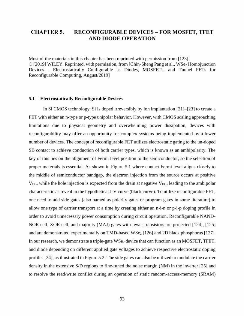
93
RECONFIGURABLE DEVICES – FOR MOSFET, TFET
AND DIODE OPERATION
Most of the materials in this chapter has been reprinted with permission from [123].
© [2019] WILEY. Reprinted, with permission, from [Chin-Sheng Pang et al., WSe2 Homojunction
Devices - Electrostatically Configurable as Diodes, MOSFETs, and Tunnel FETs for
Reconfigurable Computing, August/2019]
5.1 Electrostatically Reconfigurable Devices
In Si CMOS technology, Si is doped irreversibly by ion implantation [21]–[23] to create a
FET with either an n-type or p-type unipolar behavior. However, with CMOS scaling approaching
limitations due to physical geometry and overwhelming power dissipation, devices with
reconfigurability may offer an opportunity for complex systems being implemented by a lower
number of devices. The concept of reconfigurable FET utilizes electrostatic gating to the un-doped
SB contact to achieve conduction of both carrier types, which is known as an ambipolarity. The
key of this lies on the alignment of Fermi level position to the semiconductor, so the selection of
proper materials is essential. As shown in Figure 5.1 where contact Fermi level aligns closely to
the middle of semiconductor bandgap, the electron injection from the source occurs at positive
VBG, while the hole injection is expected from the drain at negative VBG, leading to the ambipolar
characteristic as reveal in the hypothetical I-V curve (black curve). To utilize reconfigurable FET,
one need to add side gates (also named as polarity gates or program gates in some literature) to
allow one type of carrier transport at a time by creating either an n-i-n or p-i-p doping profile in
order to avoid unnecessary power consumption during circuit operation. Reconfigurable NAND-
NOR cell, XOR cell, and majority (MAJ) gates with fewer transistors are projected [124], [125]
and are demonstrated experimentally on TMD-based WSe2 [126] and 2D black phosphorus [127].
In our research, we demonstrate a triple-gate WSe2 device that can function as an MOSFET, TFET,
and diode depending on different applied gate voltages to achieve respective electrostatic doping
profiles [24], as illustrated in Figure 5.2. The side gates can also be utilized to modulate the carrier
density in the extensive S/D regions to fine-tuned the noise margin (NM) in the inverter [25] and
to resolve the read/write conflict during an operation of static random-access-memory (SRAM)
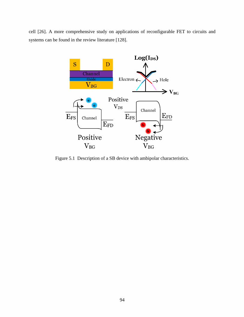
94
cell [26]. A more comprehensive study on applications of reconfigurable FET to circuits and
systems can be found in the review literature [128].
Figure 5.1 Description of a SB device with ambipolar characteristics.
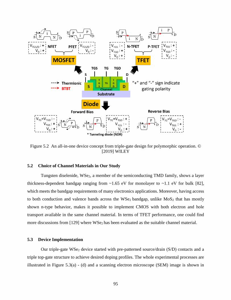
95
Figure 5.2 An all-in-one device concept from triple-gate design for polymorphic operation. ©
[2019] WILEY
5.2 Choice of Channel Materials in Our Study
Tungsten diselenide, WSe2, a member of the semiconducting TMD family, shows a layer
thickness-dependent bandgap ranging from ~1.65 eV for monolayer to ~1.1 eV for bulk [82],
which meets the bandgap requirements of many electronics applications. Moreover, having access
to both conduction and valence bands across the WSe2 bandgap, unlike MoS2 that has mostly
shown n-type behavior, makes it possible to implement CMOS with both electron and hole
transport available in the same channel material. In terms of TFET performance, one could find
more discussions from [129] where WSe2 has been evaluated as the suitable channel material.
5.3 Device Implementation
Our triple-gate WSe2 device started with pre-patterned source/drain (S/D) contacts and a
triple top-gate structure to achieve desired doping profiles. The whole experimental processes are
illustrated in Figure 5.3(a) - (d) and a scanning electron microscope (SEM) image is shown in
96
Figure 5.3(e). Raman and photoluminescence spectra are shown in the Figure 5.4(a) and (b) for
the validation of monolayer WSe2, where a single PL peak at around 1.65 eV indicates a direct
energy gap in the material [130], [131], and the vanished 1B2g Raman node at 310 cm-1 indicates
the characteristic for monolayer WSe2 exclusively, comparing to multilayers and bulk counterparts
[85]. The reason of using monolayer WSe2 is to achieve the best tunneling efficiency by optimizing
TWKB, which is discussed in section 5-4-3. During our device fabrication, Ti (2nm) /Au (10nm)
electrodes were first pre-patterned as S/D contacts with ~ 1.8 m spacing, followed by transferring
chemical vapor deposition (CVD) grown monolayer WSe2 flakes on top. Second, 1nm Al was e-
beam evaporated as a seeding layer (became 2nm Al2O3 after being exposed to atmosphere)
followed by ~4.5nm atomic layer deposition (ALD) grown HfO2 and 30nm e-beam evaporated Ni
to form two separate gate stacks on top of the extended source and drain regions, labeled as TGS
and TGD, using a lift-off process. Finally, another gate stack, TG, using the same process was
fabricated in the middle region of the channel, completing the triple top-gate structure. An atomic
force microscope (AFM) image together with the height profile are shown in Figure 5.5.
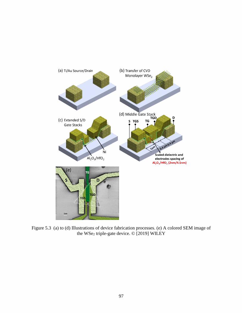
97
Figure 5.3 (a) to (d) Illustrations of device fabrication processes. (e) A colored SEM image of
the WSe2 triple-gate device. © [2019] WILEY
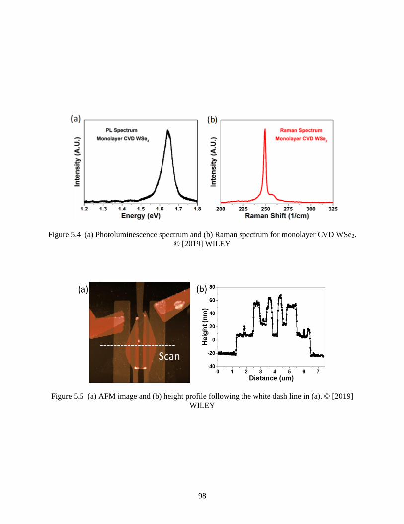
98
Figure 5.4 (a) Photoluminescence spectrum and (b) Raman spectrum for monolayer CVD WSe2.
© [2019] WILEY
Figure 5.5 (a) AFM image and (b) height profile following the white dash line in (a). © [2019]
WILEY
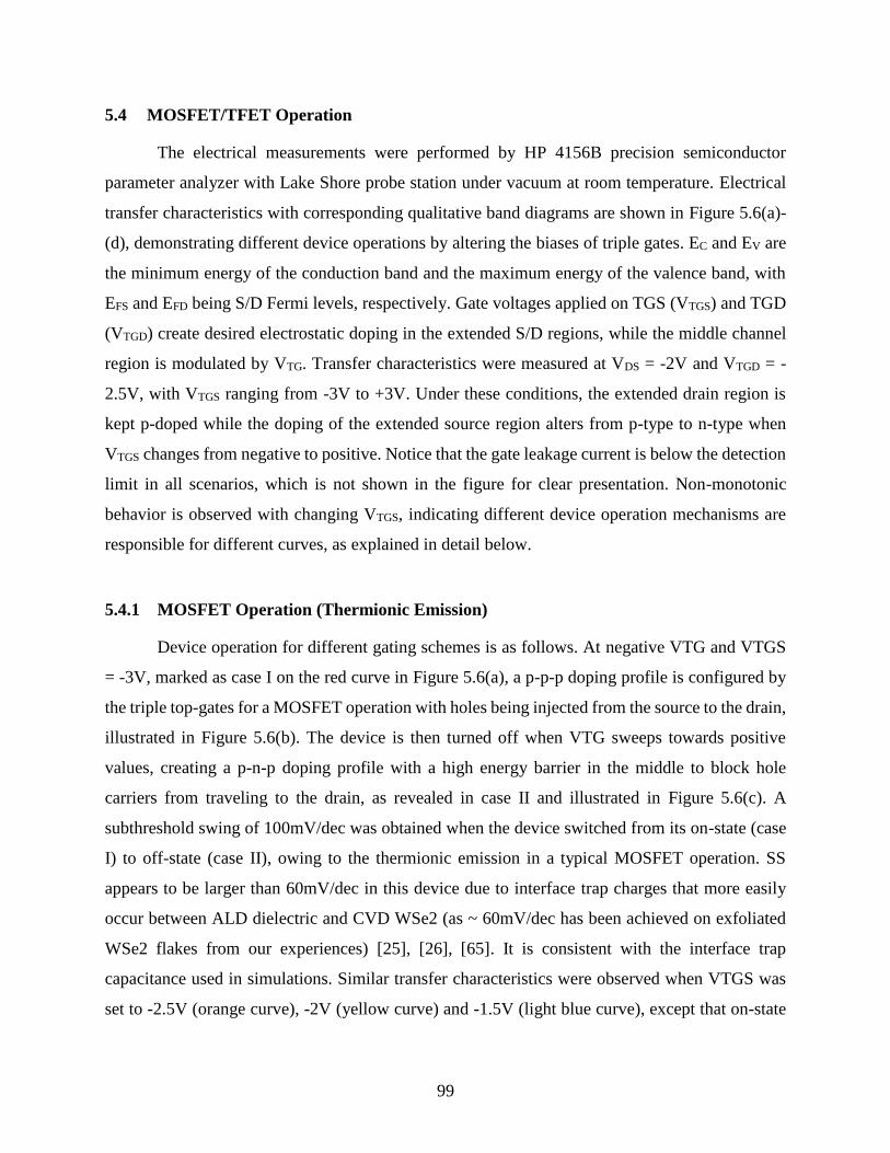
99
5.4 MOSFET/TFET Operation
The electrical measurements were performed by HP 4156B precision semiconductor
parameter analyzer with Lake Shore probe station under vacuum at room temperature. Electrical
transfer characteristics with corresponding qualitative band diagrams are shown in Figure 5.6(a)-
(d), demonstrating different device operations by altering the biases of triple gates. EC and EV are
the minimum energy of the conduction band and the maximum energy of the valence band, with
EFS and EFD being S/D Fermi levels, respectively. Gate voltages applied on TGS (VTGS) and TGD
(VTGD) create desired electrostatic doping in the extended S/D regions, while the middle channel
region is modulated by VTG. Transfer characteristics were measured at VDS = -2V and VTGD = -
2.5V, with VTGS ranging from -3V to +3V. Under these conditions, the extended drain region is
kept p-doped while the doping of the extended source region alters from p-type to n-type when
VTGS changes from negative to positive. Notice that the gate leakage current is below the detection
limit in all scenarios, which is not shown in the figure for clear presentation. Non-monotonic
behavior is observed with changing VTGS, indicating different device operation mechanisms are
responsible for different curves, as explained in detail below.
5.4.1 MOSFET Operation (Thermionic Emission)
Device operation for different gating schemes is as follows. At negative VTG and VTGS
= -3V, marked as case I on the red curve in Figure 5.6(a), a p-p-p doping profile is configured by
the triple top-gates for a MOSFET operation with holes being injected from the source to the drain,
illustrated in Figure 5.6(b). The device is then turned off when VTG sweeps towards positive
values, creating a p-n-p doping profile with a high energy barrier in the middle to block hole
carriers from traveling to the drain, as revealed in case II and illustrated in Figure 5.6(c). A
subthreshold swing of 100mV/dec was obtained when the device switched from its on-state (case
I) to off-state (case II), owing to the thermionic emission in a typical MOSFET operation. SS
appears to be larger than 60mV/dec in this device due to interface trap charges that more easily
occur between ALD dielectric and CVD WSe2 (as ~ 60mV/dec has been achieved on exfoliated
WSe2 flakes from our experiences) [25], [26], [65]. It is consistent with the interface trap
capacitance used in simulations. Similar transfer characteristics were observed when VTGS was
set to -2.5V (orange curve), -2V (yellow curve) and -1.5V (light blue curve), except that on-state
100
currents decrease with increasing VTGS. This trend is expected since fewer states are available in
the extended source region to accept hole injection from the source when its valence band edge is
pulled below EFS. In addition, the contact resistance increases significantly with less gating from
VTGS on the SB contact between the source and the extended source region. While we have
focused on p-type MOSFET operation here, biasing VTGD and VTGS at positive voltages to reach
the n-type operation is presented in Figure 5.7, demonstrating the tunability through electrostatic
gating. Output characteristics biased under both p-type and n-type configurations are provided in
Figure 5.8 as well.
5.4.2 TFET Operation (Band-to-band Tunneling)
Nevertheless, the transitioning towards TFET operation is observed when currents begin
to increase with VTGS changes from +1V (dark blue curve) and eventually reaches +3V (purple
curve) shown in Figure 5.6(a). Under the positively biased VTGS, an n-i-p doping profile is
established in the WSe2 channel. As revealed in case III and illustrated in Figure 5.6(d), with
sufficiently positive VTGS and negative VTG being applied, electron carriers injected from the
source are able to tunnel from the conduction band of the extended source region to the valence
band of the middle channel region and eventually travel to the drain contact. This is the so-called
BTBT operation. At VTGS = +3V, the higher n-doping level in the extended source region increases
the energy window (E) for tunneling, leading to a higher BTBT current compared to that at VTGS
= +1V and the observation of SS ~ 151mV/dec, the best reported SS among all homojunction
TFETs fabricated on 2D materials to the best of our knowledge [24], [132], [133]. The transition
from MOSFET to TFET operation is observed in all of our triple-gate WSe2 devices. Another
device using a multi-layer WSe2 channel is presented in Figure 5.9, showing both n-MOSFET to
n-TFET and p-MOSFET to p-TFET transitions.
Now, let’s try to understand this SS value and explore how to improve it in TFETs. While
SS of a MOSFET is expected to be a constant due to the thermionic emission over the energy
barrier of the p-n junction, SS of a TFET can overcome the thermionic limitation and in principle
become much smaller than 60mV/dec at room temperature since the highly energetic carriers from
the Fermi distribution are blocked by the bandgap through the BTBT mechanism (illustrated in
Figure 5.6(d)). However, the resulted SS is strongly dependent on the electrostatic screening length

101
, which describes the spatial extent of the tunneling barrier and is given by ch ox ch oxλ= (ε /ε )T T
[56], where Tch is the channel thickness, Tox is the oxide thickness, ch and ox are the dielectric
constant of channel and oxide, respectively. is not yet sufficiently minimized to achieve SS of
sub 60mV/dec in our current demonstration due to the relatively thick gate oxide used in our device
fabrication. High quality, scaled gate dielectrics are obviously required to achieve a smaller
screening length. Novel approaches of realizing ultra-thin oxide with sub-nm thickness will
certainly benefit the scaling [134]. The large SS of 151mV/dec can be greatly improved once the
optimal design is adopted as discussed next.
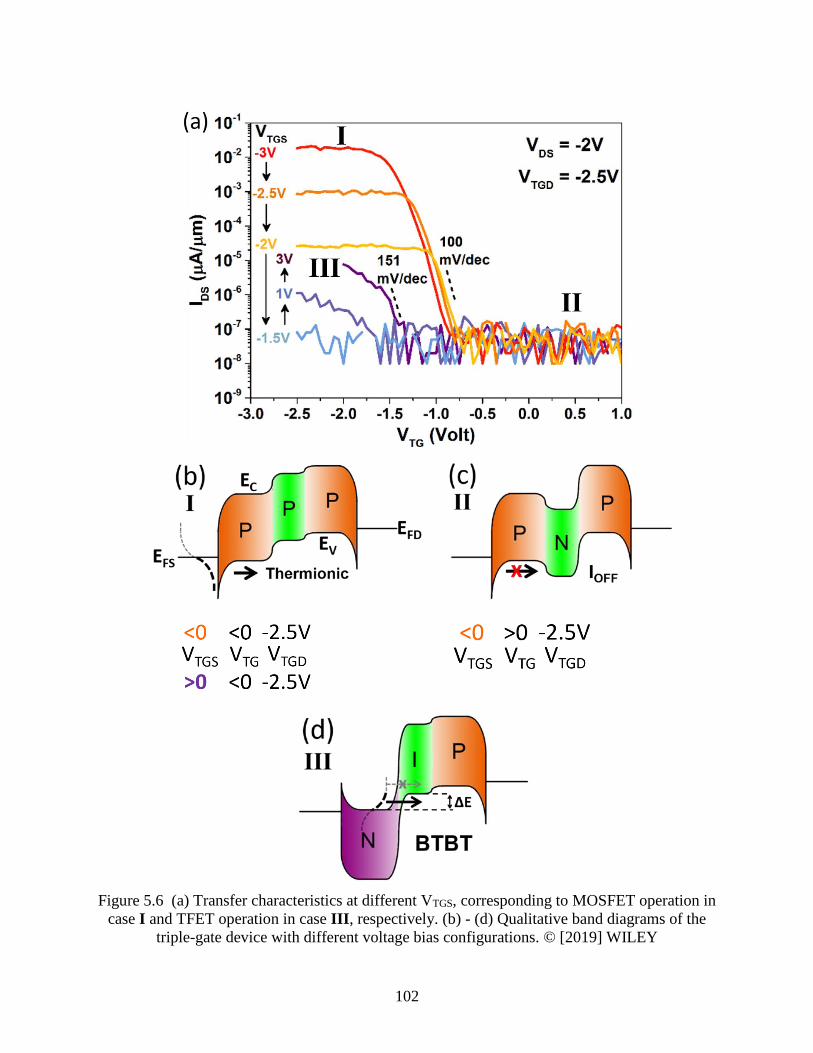
102
Figure 5.6 (a) Transfer characteristics at different VTGS, corresponding to MOSFET operation in
case I and TFET operation in case III, respectively. (b) - (d) Qualitative band diagrams of the
triple-gate device with different voltage bias configurations. © [2019] WILEY
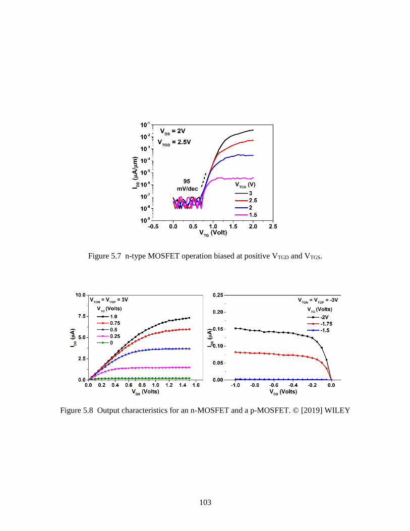
103
Figure 5.7 n-type MOSFET operation biased at positive VTGD and VTGS.
Figure 5.8 Output characteristics for an n-MOSFET and a p-MOSFET. © [2019] WILEY
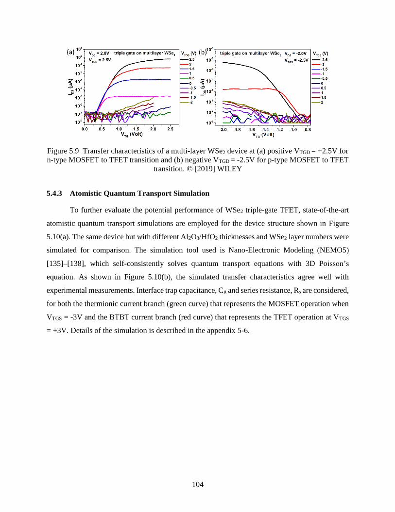
104
Figure 5.9 Transfer characteristics of a multi-layer WSe2 device at (a) positive VTGD = +2.5V for
n-type MOSFET to TFET transition and (b) negative VTGD = -2.5V for p-type MOSFET to TFET
transition. © [2019] WILEY
5.4.3 Atomistic Quantum Transport Simulation
To further evaluate the potential performance of WSe2 triple-gate TFET, state-of-the-art
atomistic quantum transport simulations are employed for the device structure shown in Figure
5.10(a). The same device but with different Al2O3/HfO2 thicknesses and WSe2 layer numbers were
simulated for comparison. The simulation tool used is Nano-Electronic Modeling (NEMO5)
[135]–[138], which self-consistently solves quantum transport equations with 3D Poisson’s
equation. As shown in Figure 5.10(b), the simulated transfer characteristics agree well with
experimental measurements. Interface trap capacitance, Cit and series resistance, Rs are considered,
for both the thermionic current branch (green curve) that represents the MOSFET operation when
VTGS = -3V and the BTBT current branch (red curve) that represents the TFET operation at VTGS
= +3V. Details of the simulation is described in the appendix 5-6.
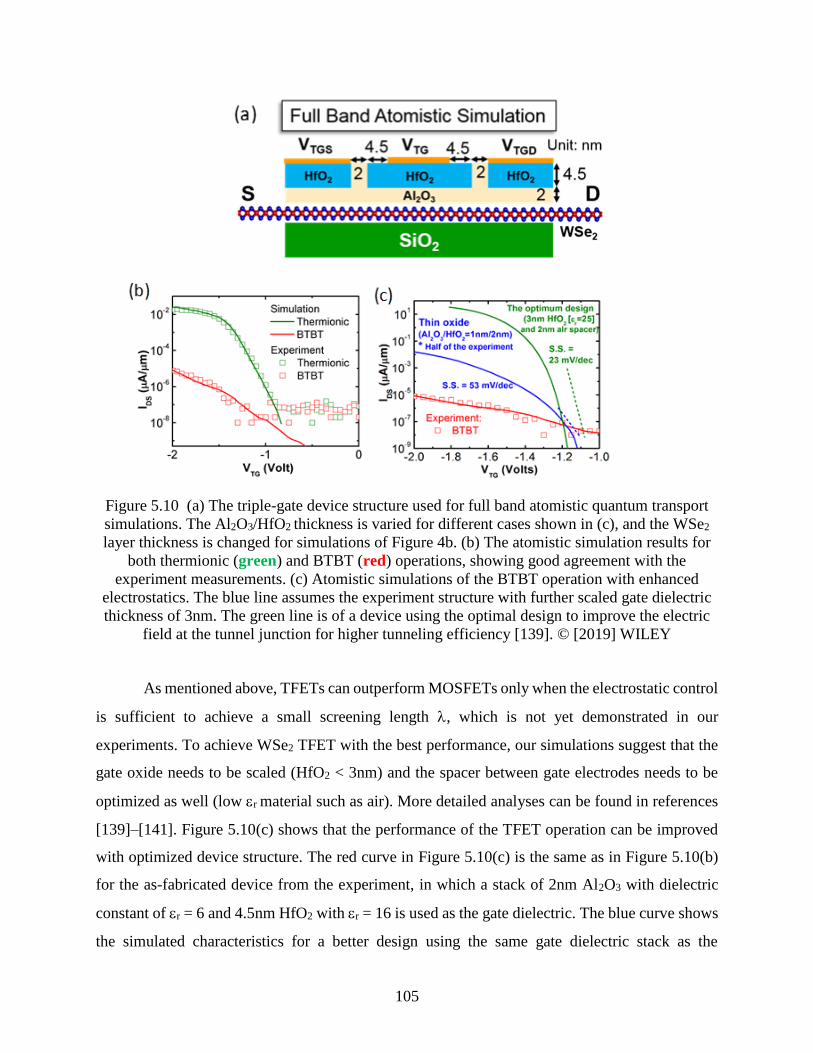
105
Figure 5.10 (a) The triple-gate device structure used for full band atomistic quantum transport
simulations. The Al2O3/HfO2 thickness is varied for different cases shown in (c), and the WSe2
layer thickness is changed for simulations of Figure 4b. (b) The atomistic simulation results for
both thermionic (green) and BTBT (red) operations, showing good agreement with the
experiment measurements. (c) Atomistic simulations of the BTBT operation with enhanced
electrostatics. The blue line assumes the experiment structure with further scaled gate dielectric
thickness of 3nm. The green line is of a device using the optimal design to improve the electric
field at the tunnel junction for higher tunneling efficiency [139]. © [2019] WILEY
As mentioned above, TFETs can outperform MOSFETs only when the electrostatic control
is sufficient to achieve a small screening length , which is not yet demonstrated in our
experiments. To achieve WSe2 TFET with the best performance, our simulations suggest that the
gate oxide needs to be scaled (HfO2 < 3nm) and the spacer between gate electrodes needs to be
optimized as well (low r material such as air). More detailed analyses can be found in references
[139]–[141]. Figure 5.10(c) shows that the performance of the TFET operation can be improved
with optimized device structure. The red curve in Figure 5.10(c) is the same as in Figure 5.10(b)
for the as-fabricated device from the experiment, in which a stack of 2nm Al2O3 with dielectric
constant of r = 6 and 4.5nm HfO2 with r = 16 is used as the gate dielectric. The blue curve shows
the simulated characteristics for a better design using the same gate dielectric stack as the
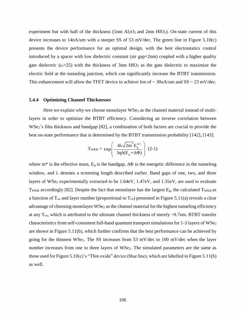
106
experiment but with half of the thickness (1nm Al2O3 and 2nm HfO2). On-state current of this
device increases to 14nA/um with a steeper SS of 53 mV/dec. The green line in Figure 5.10(c)
presents the device performance for an optimal design, with the best electrostatics control
introduced by a spacer with low dielectric constant (air gap=2nm) coupled with a higher quality
gate dielectric (r=25) with the thickness of 3nm HfO2 as the gate dielectric to maximize the
electric field at the tunneling junction, which can significantly increase the BTBT transmission.
This enhancement will allow the TFET device to achieve Ion of ~ 30uA/um and SS ~ 23 mV/dec.
5.4.4 Optimizing Channel Thicknesses
Here we explain why we choose monolayer WSe2 as the channel material instead of multi-
layers in order to optimize the BTBT efficiency. Considering an inverse correlation between
WSe2’s film thickness and bandgap [82], a combination of both factors are crucial to provide the
best on-state performance that is determined by the BTBT transmission probability [142], [143]:
TWKB = * 3/2
g
g
4λ 2m Eexp -
3q (E +ΔΦ)
(2-1)
where m* is the effective mass, Eg is the bandgap, is the energetic difference in the tunneling
window, and denotes a screening length described earlier. Band gaps of one, two, and three
layers of WSe2 experimentally extracted to be 1.64eV, 1.47eV, and 1.35eV, are used to evaluate
TWKB accordingly [82]. Despite the fact that monolayer has the largest Eg, the calculated TWKB as
a function of Tox and layer number (proportional to Tch) presented in Figure 5.11(a) reveals a clear
advantage of choosing monolayer WSe2 as the channel material for the highest tunneling efficiency
at any Tox, which is attributed to the ultimate channel thickness of merely ~0.7nm. BTBT transfer
characteristics from self-consistent full-band quantum transport simulations for 1-3 layers of WSe2
are shown in Figure 5.11(b), which further confirms that the best performance can be achieved by
going for the thinnest WSe2. The SS increases from 53 mV/dec to 100 mV/dec when the layer
number increases from one to three layers of WSe2. The simulated parameters are the same as
those used for Figure 5.10(c)’s “Thin oxide” device (blue line), which are labelled in Figure 5.11(b)
as well.
107
Figure 5.11 (a) The calculated TWKB vs Tox (HfO2 with r = 16) and WSe2 layer number shows
monolayer WSe2 is the best choice for TFET device. (b) The simulated BTBT behavior on 1-3
layers of WSe2 with Tox = 3nm based on the self-consistent full-band atomistic quantum
transport. © [2019] WILEY
5.5 Diode Operation
As shown in Figure 5.2, the device can also operate as a diode. Notice that the diode
operation can be accomplished by simply applying the same voltage to both the TG and TGD
electrodes in the triple-gate device. However, if one only requires the diode operation alone, a
double top-gate WSe2 device can be fabricated for simplicity using identical processes mentioned
in the section 5-3. The structure is illustrated in Figure 5.12(a). When the two gates are tied together
for the as-fabricated double-gate device (TGD and TGS of Figure 5.12(a)), the expected ambipolar
characteristics for a 2D Schottky-barrier transistor along with a high on/off current ratio are
obtained, as shown in Figure 5.12(b) – another example of configuring the device to the desired
operation mode by altering the doping profile in the channel.
Now let’s switch to the diode operation with the best ideality factor being observed up to
date. Different from conventional p-n junction devices where the doping profile is pre-determined
by implantation/chemical doping, our p-n diode relies on electrostatic doping through the gate field
as described in the previous transistor section. We will first analyze p-n diode operation under
forward bias with various VTGS and VTGD, then discuss BTBT transport at reverse bias. Figure
5.12(c) shows the experimentally measured diode current as a function of VDS, with VTGD = -3V
and VTGS varying from 2.6V to 1.25V indicated by different colors. An n-p doping profile is created
by the double-gate and a positive VDS sets the diode to forward bias operation which leads to the
device on-state. Ideally, the forward bias current should increase exponentially with VDS due to the
108
thermionic emission over the n-p junction, with the band profile described in case I. However, a
series resistance RS associated with the SB at the interface between the metal contact and the WSe2
channel has to be taken into account, as described by the extended Shockley diode equation:
DS DS SDS S
T
V -I RI =I exp -1
nV
(2-2)
where VT = kBT/q is the thermal voltage at temperature T, q is the elementary charge, kB is the
Boltzmann constant, IS is the reverse saturation current and n is the diode ideality factor, which
has an ideal value of 1. An ideality factor of ~ 1.5 is extracted from fitting the IDS-VDS curves (only
4 curves with VTGS ranging from 2.6V to 2.0V were fitted), implying both diffusion and
recombination currents are responsible for the conduction. Notice that the ideality factor of our p-
n diode is better compared to earlier studies [144], [145], suggesting that our top-gate design with
a small spacing between the two gates (~6nm gate oxide becomes the spacer) is able to eliminate
un-doped channel region to a large extent and form a well-controlled n-p junction.
While VTGS controls the n-type doping level in the channel segment next to the source, it
also modulates the contact resistance, RS, associated with the source SB. Rs increases from 12M
to 128M when VTGS decreases from 2.6V to 2.0V. When VTGS is further decreased, RS increases
rapidly as expected. Interestingly, an upturn of current is observed at large VDS for VTGS = 1.25V
and 1.5V. The effective electric field for the electrostatic doping in the WSe2 channel next to the
drain is proportional to VTGD - VDS. When sufficiently positive VDS is applied, the band bending
in the extended drain region gets pulled down and holes start to be injected from the drain into the
channel and leave the source, as shown in the band diagram of case II. It is easy to understand that
lower doping in the N-region (VTGS = 1.25V compared to VTGS = 1.5V) will result in an earlier
onset of IDS upturn at smaller VDS since holes can get to the source more easily without a barrier
across the n-p junction.
Next, we focus on reverse bias conditions at which BTBT is observed. As shown in Figure
5.12(d), VTGD scans from 2V to -3V with VDS = -2V and VTGS applied at 2.75V and -0.25V. The
band diagram and working principle for these two gating scenarios are illustrated as insets. At
VTGS = 2.75V and positive VTGD being applied with reverse bias of VDS = -2V, thermionic emission
dominates the conduction with electrons being injected from the drain and traveling to the source.
The current conduction is then turned off with decreased VTGD by blocking carrier injection in the
n-p junction under the same reverse bias. Nevertheless, the current starts to get enhanced with
109
sufficiently negative VTGD being applied, as revealed in the shaded purple region. The n-p doping
profile is established in this stage as shown in the upper left inset, and carriers injected from the
source can now tunnel through the energy window and travel to the drain, which forms the gate
controlled BTBT current. When VTGS = -0.25V, the thermionic emission at positive VTGD is
suppressed due to fewer available states in the channel and higher RS associated with the source
SB. The BTBT at negative VTGD is suppressed as well since lower doping in the N-region leads to
a decreased tunneling efficiency. Diode current as a function of two gates are mapped out in Figure
5.12(e) with different operation modes labeled. The thermionic emission in n-n doping
configuration towards BTBT behavior in n-p doping profile are comprehended.
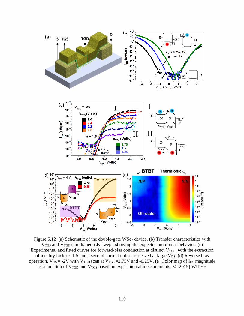
110
Figure 5.12 (a) Schematic of the double-gate WSe2 device. (b) Transfer characteristics with
VTGS and VTGD simultaneously swept, showing the expected ambipolar behavior. (c)
Experimental and fitted curves for forward-bias conduction at distinct VTGS, with the extraction
of ideality factor ~ 1.5 and a second current upturn observed at large VDS. (d) Reverse bias
operation, VDS = -2V with VTGD scan at VTGS =2.75V and -0.25V. (e) Color map of IDS magnitude
as a function of VTGD and VTGS based on experimental measurements. © [2019] WILEY
111
5.6 Appendix
The atomistic quantum transport simulations (AQTM) are conducted by coupling quantum
transmitting boundary method (QTBM) and 3D-Poisson equation [138], [139]. QTBM is a
computationally efficient method to solve an open boundary Schrödinder equation without
considering scattering.
(EI−H −Σ)ψ = S (2-3)
Equation 2-3 is an open boundary Schrödinder equation solved in QTBM where E, I, and H are
energy, identity matrix, and device Hamiltonian. Σ is the self-energy due to an open boundary
condition. ψ and S are the wave function in the device and the strength of the carrier injection from
the source and the drain. NEMO5 (Nanoelectronics modeling tool) is used to perform the
simulation. The Hamiltonian is constructed using tight binding method and assumes second nearest
neighbor coupling. More details on the simulation can be found in [136], [140], [141]
The QTBM simulation provides an ideal intrinsic device characteristic that does not
include scattering such that the current and the SS can be overestimated. To include the non-ideal
factors, the interface trap capacitance (Cit) and the series resistance (Rs) are considered as shown
in Figure 5.13(a). Cit degrades the ideal gate control while 𝑅𝑠 reduces the ideal current level.
VTG = (1 +Cit
Cox)VTG.sim (2-4)
Where Cox is the oxide capacitance and 𝑉𝑔.𝑠𝑖𝑚 is the gate voltage used in the simulation.
IDS =IDS.sim
1+G0Rs (2-5)
Where 𝐺0 is the channel conductance obtained from the simulation (=dVTG.sim
dIDS.sim) where IDS.sim is
the current obtained from the simulation.
Figure 5.13(b) shows the ideal transfer characteristics (solid curve) when Cit and Rs are
considered negligible in the simulations. For the thermionic operation, the ideal transfer
characteristics has much better IDS and SS compared to the experimental result (green hollow curve)
which includes Cit =0.75 Cox and Rs = 3M·m. For the BTBT operation, the performance
between experimental and simulated results (red hollow and solid curves) in Figure 5.13(b) do not
have much difference because the tunneling resistance in the channel dominates the performance.
Please note that, for the BTBT simulation results presented in Figure 5.10(c) (the blue line and the
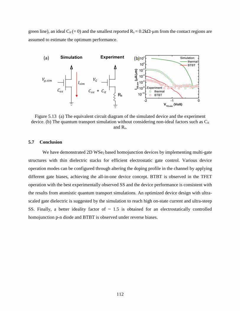
112
green line), an ideal Cit (= 0) and the smallest reported Rs = 0.2k·m from the contact regions are
assumed to estimate the optimum performance.
Figure 5.13 (a) The equivalent circuit diagram of the simulated device and the experiment
device. (b) The quantum transport simulation without considering non-ideal factors such as Cit
and Rs.
5.7 Conclusion
We have demonstrated 2D WSe2 based homojunction devices by implementing multi-gate
structures with thin dielectric stacks for efficient electrostatic gate control. Various device
operation modes can be configured through altering the doping profile in the channel by applying
different gate biases, achieving the all-in-one device concept. BTBT is observed in the TFET
operation with the best experimentally observed SS and the device performance is consistent with
the results from atomistic quantum transport simulations. An optimized device design with ultra-
scaled gate dielectric is suggested by the simulation to reach high on-state current and ultra-steep
SS. Finally, a better ideality factor of ~ 1.5 is obtained for an electrostatically controlled
homojunction p-n diode and BTBT is observed under reverse biases.
113
WSE2 CMOS-BASED INVERTER AND SRAM
Most of the materials in this chapter has been reprinted with permission from [25], [26].
© [2018] IEEE. Reprinted, with permission, from [Chin-Sheng Pang et al., First Demonstration of
WSe2 CMOS Inverter with Modulable Noise Margin by Electrostatic Doping, June/2018]
© [2018] IEEE. Reprinted, with permission, from [Chin-Sheng Pang et al., First Demonstration of
WSe2 Based CMOS-SRAM, December/2018]
6.1 From Device to Circuit Applications
In the last chapter, we discussed how electrostatically configurable triple-gate WSe2 device
can be functioned as MOSFET, TFET, and diode by tuning the channel doping to the desired
profile, enabling polymorphic operation. In this chapter, we will demonstrate how this novel gating
scheme can be applied to circuit applications. We demonstrate a WSe2-based CMOS inverter with
modulable noise margin (NM), full logic swing, and high voltage gain. We also demonstrate a
CMOS SRAM with dynamic tunability by electrostatic gating to resolve the read/write (R/W)
conflict in the SRAM operation. In addition, by exploiting R/W assist techniques, our design yields
enhanced SRAM stability, enabling operation at low VDD = 0.8V.
6.2 Inverter Implementation and Demonstration
6.2.1 Triple-gate WSe2 as n/p-FET
The design of triple-gate WSe2 device shares similarity as discussed in Figure 5.3 from
chapter V, except the exfoliated multilayer WSe2 was used as the channel material. To operate as
an inverter, the drain contacts of the n-FET and p-FET were connected on-chip through a metal
line as illustrated in Figure 6.1. Noticed that the inverter can be implemented on a monolithic flake
given a sufficient size of it.
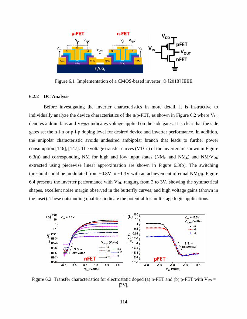
114
Figure 6.1 Implementation of a CMOS-based inverter. © [2018] IEEE
6.2.2 DC Analysis
Before investigating the inverter characteristics in more detail, it is instructive to
individually analyze the device characteristics of the n/p-FET, as shown in Figure 6.2 where VDS
denotes a drain bias and VTGNP indicates voltage applied on the side gates. It is clear that the side
gates set the n-i-n or p-i-p doping level for desired device and inverter performance. In addition,
the unipolar characteristic avoids undesired ambipolar branch that leads to further power
consumption [146], [147]. The voltage transfer curves (VTCs) of the inverter are shown in Figure
6.3(a) and corresponding NM for high and low input states (NMH and NML) and NM/VDD
extracted using piecewise linear approximation are shown in Figure 6.3(b). The switching
threshold could be modulated from ~0.8V to ~1.3V with an achievement of equal NML/H. Figure
6.4 presents the inverter performance with VDD ranging from 2 to 3V, showing the symmetrical
shapes, excellent noise margin observed in the butterfly curves, and high voltage gains (shown in
the inset). These outstanding qualities indicate the potential for multistage logic applications.
Figure 6.2 Transfer characteristics for electrostatic doped (a) n-FET and (b) p-FET with VDS =
|2V|.
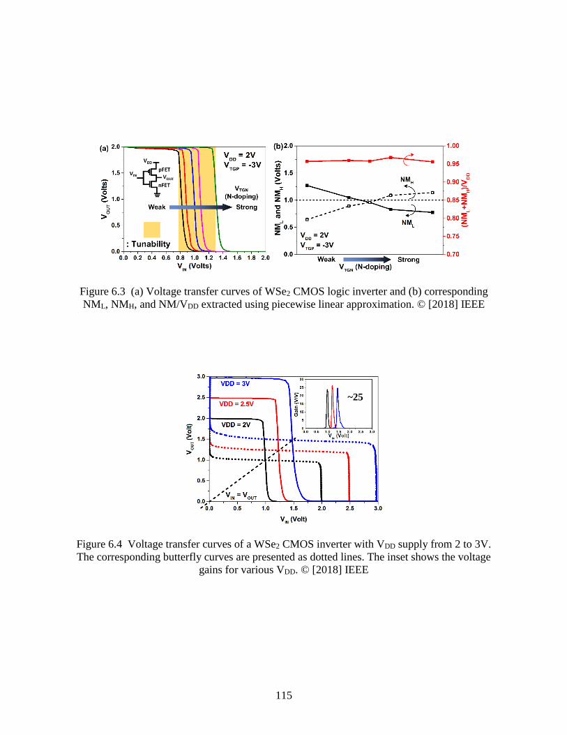
115
Figure 6.3 (a) Voltage transfer curves of WSe2 CMOS logic inverter and (b) corresponding
NML, NMH, and NM/VDD extracted using piecewise linear approximation. © [2018] IEEE
Figure 6.4 Voltage transfer curves of a WSe2 CMOS inverter with VDD supply from 2 to 3V.
The corresponding butterfly curves are presented as dotted lines. The inset shows the voltage
gains for various VDD. © [2018] IEEE
~25
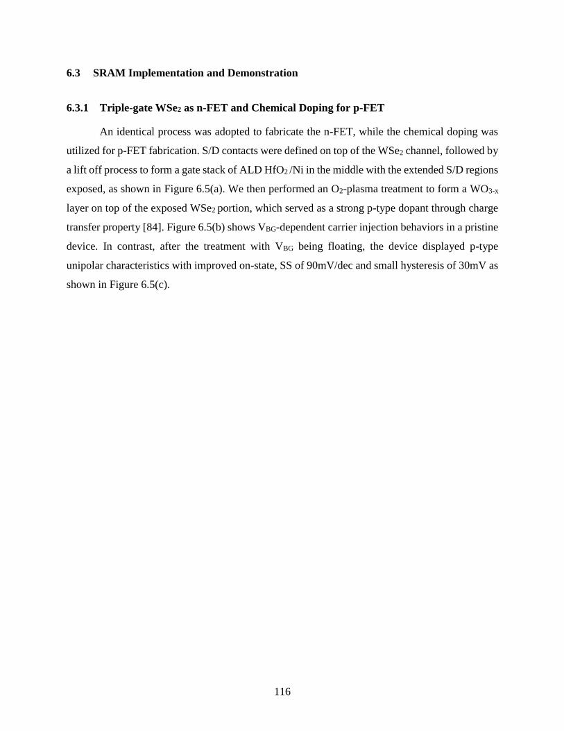
116
6.3 SRAM Implementation and Demonstration
6.3.1 Triple-gate WSe2 as n-FET and Chemical Doping for p-FET
An identical process was adopted to fabricate the n-FET, while the chemical doping was
utilized for p-FET fabrication. S/D contacts were defined on top of the WSe2 channel, followed by
a lift off process to form a gate stack of ALD HfO2 /Ni in the middle with the extended S/D regions
exposed, as shown in Figure 6.5(a). We then performed an O2-plasma treatment to form a WO3-x
layer on top of the exposed WSe2 portion, which served as a strong p-type dopant through charge
transfer property [84]. Figure 6.5(b) shows VBG-dependent carrier injection behaviors in a pristine
device. In contrast, after the treatment with VBG being floating, the device displayed p-type
unipolar characteristics with improved on-state, SS of 90mV/dec and small hysteresis of 30mV as
shown in Figure 6.5(c).
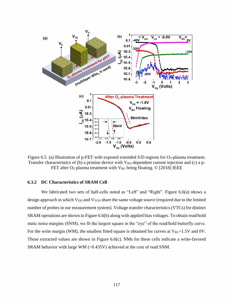
117
Figure 6.5 (a) Illustration of p-FET with exposed extended S/D regions for O2-plasma treatment.
Transfer characteristics of (b) a pristine device with VBG-dependent current injection and (c) a p-
FET after O2-plasma treatment with VBG being floating. © [2018] IEEE
6.3.2 DC Characteristics of SRAM Cell
We fabricated two sets of half-cells noted as “Left” and “Right”. Figure 6.6(a) shows a
design approach in which VDD and VTGN share the same voltage source (required due to the limited
number of probes in our measurement system). Voltage transfer characteristics (VTCs) for distinct
SRAM operations are shown in Figure 6.6(b) along with applied bias voltages. To obtain read/hold
static noise margins (SNM), we fit the largest square in the “eye” of the read/hold butterfly curve.
For the write margin (WM), the smallest fitted square is obtained for curves at VBL=1.5V and 0V.
Those extracted values are shown in Figure 6.6(c). NMs for these cells indicate a write-favored
SRAM behavior with large WM (~0.435V) achieved at the cost of read SNM.
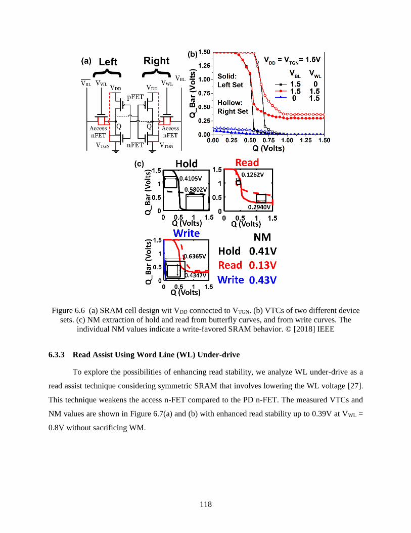
118
Figure 6.6 (a) SRAM cell design wit VDD connected to VTGN. (b) VTCs of two different device
sets. (c) NM extraction of hold and read from butterfly curves, and from write curves. The
individual NM values indicate a write-favored SRAM behavior. © [2018] IEEE
6.3.3 Read Assist Using Word Line (WL) Under-drive
To explore the possibilities of enhancing read stability, we analyze WL under-drive as a
read assist technique considering symmetric SRAM that involves lowering the WL voltage [27].
This technique weakens the access n-FET compared to the PD n-FET. The measured VTCs and
NM values are shown in Figure 6.7(a) and (b) with enhanced read stability up to 0.39V at VWL =
0.8V without sacrificing WM.
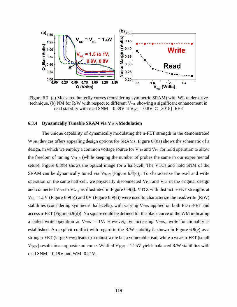
119
Figure 6.7 (a) Measured butterfly curves (considering symmetric SRAM) with WL under-drive
technique. (b) NM for R/W with respect to different VWL showing a significant enhancement in
read stability with read SNM = 0.39V at VWL = 0.8V. © [2018] IEEE
6.3.4 Dynamically Tunable SRAM via VTGN Modulation
The unique capability of dynamically modulating the n-FET strength in the demonstrated
WSe2 devices offers appealing design options for SRAMs. Figure 6.8(a) shows the schematic of a
design, in which we employ a common voltage source for VDD and VBL for hold operation to allow
the freedom of tuning VTGN (while keeping the number of probes the same in our experimental
setup). Figure 6.8(b) shows the optical image for a half-cell. The VTCs and hold SNM of the
SRAM can be dynamically tuned via VTGN (Figure 6.8(c)). To characterize the read and write
operation on the same half-cell, we physically disconnected VDD and VBL in the original design
and connected VDD to VWL, as illustrated in Figure 6.9(a). VTCs with distinct n-FET strengths at
VBL =1.5V (Figure 6.9(b)) and 0V (Figure 6.9(c)) were used to characterize the read/write (R/W)
stabilities (considering symmetric half-cells), with varying VTGN applied on both PD n-FET and
access n-FET (Figure 6.9(d)). No square could be defined for the black curve of the WM indicating
a failed write operation at VTGN = 1V. However, by increasing VTGN, write functionality is
established. An explicit conflict with regard to the R/W stability is shown in Figure 6.9(e) as a
strong n-FET (large VTGN) leads to a robust write but a vulnerable read, while a weak n-FET (small
VTGN) results in an opposite outcome. We find VTGN = 1.25V yields balanced R/W stabilities with
read SNM = 0.19V and WM=0.21V.
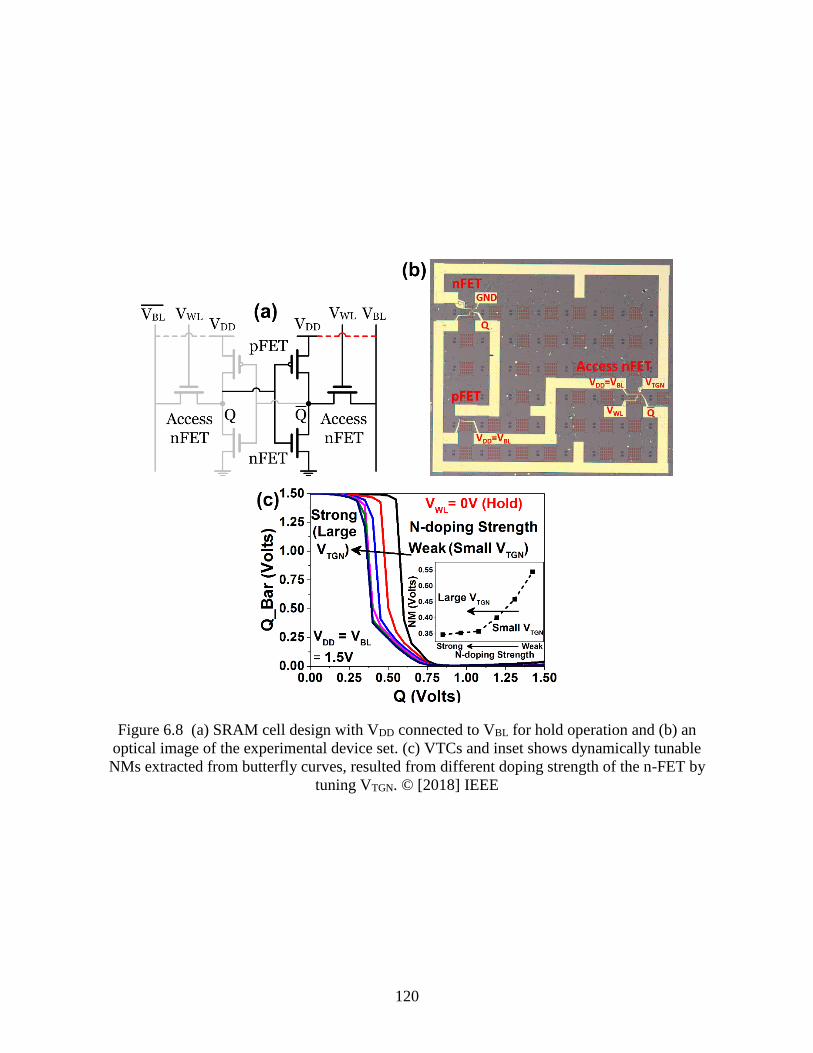
120
Figure 6.8 (a) SRAM cell design with VDD connected to VBL for hold operation and (b) an
optical image of the experimental device set. (c) VTCs and inset shows dynamically tunable
NMs extracted from butterfly curves, resulted from different doping strength of the n-FET by
tuning VTGN. © [2018] IEEE
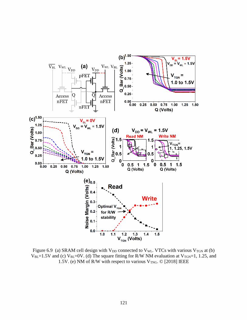
121
Figure 6.9 (a) SRAM cell design with VDD connected to VWL. VTCs with various VTGN at (b)
VBL=1.5V and (c) VBL=0V. (d) The square fitting for R/W NM evaluation at VTGN=1, 1.25, and
1.5V. (e) NM of R/W with respect to various VTNG. © [2018] IEEE
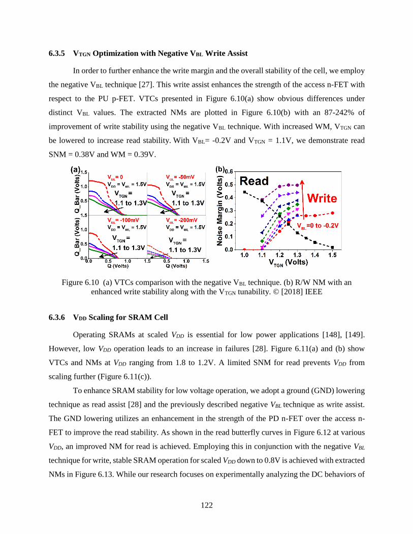
122
6.3.5 VTGN Optimization with Negative VBL Write Assist
In order to further enhance the write margin and the overall stability of the cell, we employ
the negative VBL technique [27]. This write assist enhances the strength of the access n-FET with
respect to the PU p-FET. VTCs presented in Figure 6.10(a) show obvious differences under
distinct VBL values. The extracted NMs are plotted in Figure 6.10(b) with an 87-242% of
improvement of write stability using the negative VBL technique. With increased WM, VTGN can
be lowered to increase read stability. With VBL= -0.2V and VTGN = 1.1V, we demonstrate read
SNM = 0.38V and WM = 0.39V.
Figure 6.10 (a) VTCs comparison with the negative VBL technique. (b) R/W NM with an
enhanced write stability along with the VTGN tunability. © [2018] IEEE
6.3.6 VDD Scaling for SRAM Cell
Operating SRAMs at scaled VDD is essential for low power applications [148], [149].
However, low VDD operation leads to an increase in failures [28]. Figure 6.11(a) and (b) show
VTCs and NMs at VDD ranging from 1.8 to 1.2V. A limited SNM for read prevents VDD from
scaling further (Figure 6.11(c)).
To enhance SRAM stability for low voltage operation, we adopt a ground (GND) lowering
technique as read assist [28] and the previously described negative VBL technique as write assist.
The GND lowering utilizes an enhancement in the strength of the PD n-FET over the access n-
FET to improve the read stability. As shown in the read butterfly curves in Figure 6.12 at various
VDD, an improved NM for read is achieved. Employing this in conjunction with the negative VBL
technique for write, stable SRAM operation for scaled VDD down to 0.8V is achieved with extracted
NMs in Figure 6.13. While our research focuses on experimentally analyzing the DC behaviors of
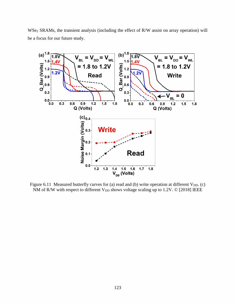
123
WSe2 SRAMs, the transient analysis (including the effect of R/W assist on array operation) will
be a focus for our future study.
Figure 6.11 Measured butterfly curves for (a) read and (b) write operation at different VDD. (c)
NM of R/W with respect to different VDD shows voltage scaling up to 1.2V. © [2018] IEEE
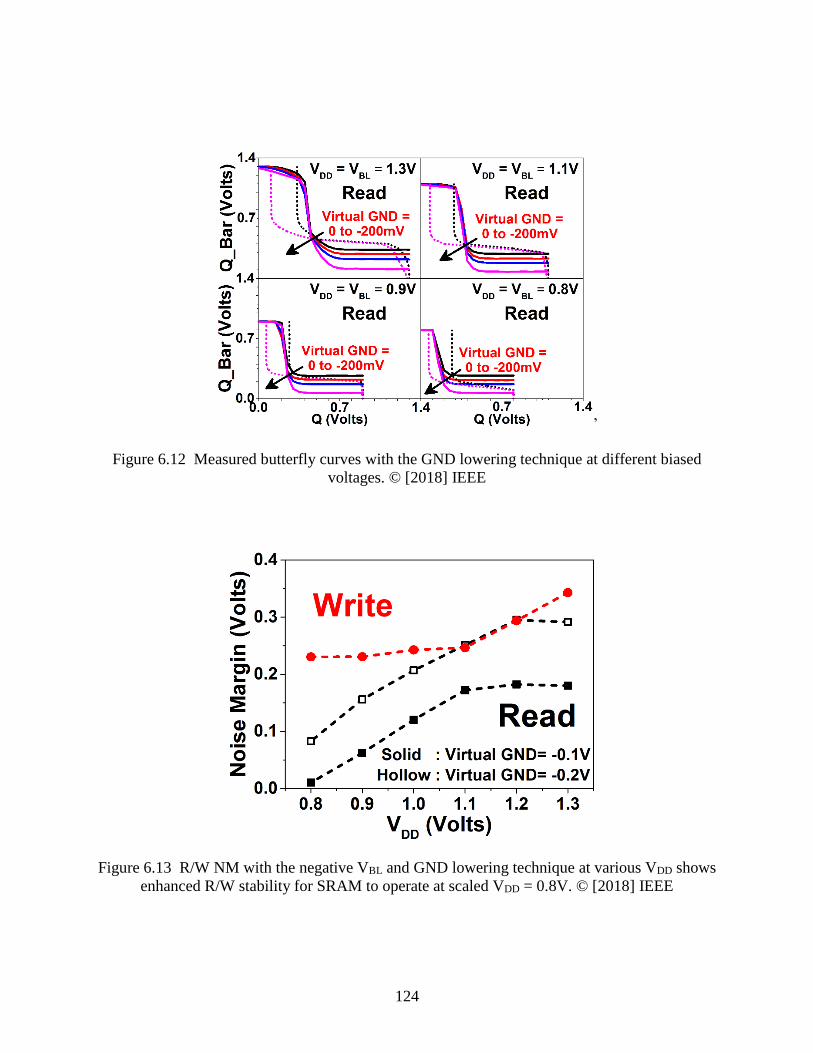
124
’
Figure 6.12 Measured butterfly curves with the GND lowering technique at different biased
voltages. © [2018] IEEE
Figure 6.13 R/W NM with the negative VBL and GND lowering technique at various VDD shows
enhanced R/W stability for SRAM to operate at scaled VDD = 0.8V. © [2018] IEEE
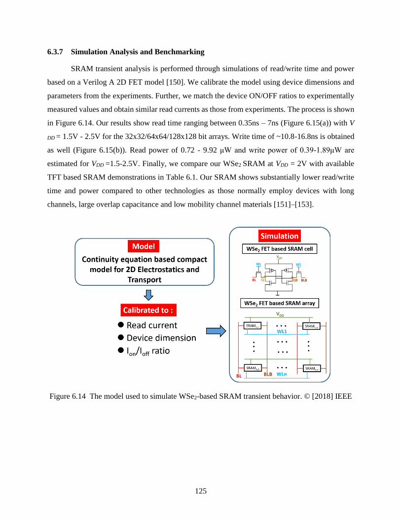
125
6.3.7 Simulation Analysis and Benchmarking
SRAM transient analysis is performed through simulations of read/write time and power
based on a Verilog A 2D FET model [150]. We calibrate the model using device dimensions and
parameters from the experiments. Further, we match the device ON/OFF ratios to experimentally
measured values and obtain similar read currents as those from experiments. The process is shown
in Figure 6.14. Our results show read time ranging between 0.35ns – 7ns (Figure 6.15(a)) with V
DD = 1.5V - 2.5V for the 32x32/64x64/128x128 bit arrays. Write time of ~10.8-16.8ns is obtained
as well (Figure 6.15(b)). Read power of 0.72 - 9.92 μW and write power of 0.39-1.89μW are
estimated for VDD =1.5-2.5V. Finally, we compare our WSe2 SRAM at VDD = 2V with available
TFT based SRAM demonstrations in Table 6.1. Our SRAM shows substantially lower read/write
time and power compared to other technologies as those normally employ devices with long
channels, large overlap capacitance and low mobility channel materials [151]–[153].
Figure 6.14 The model used to simulate WSe2-based SRAM transient behavior. © [2018] IEEE
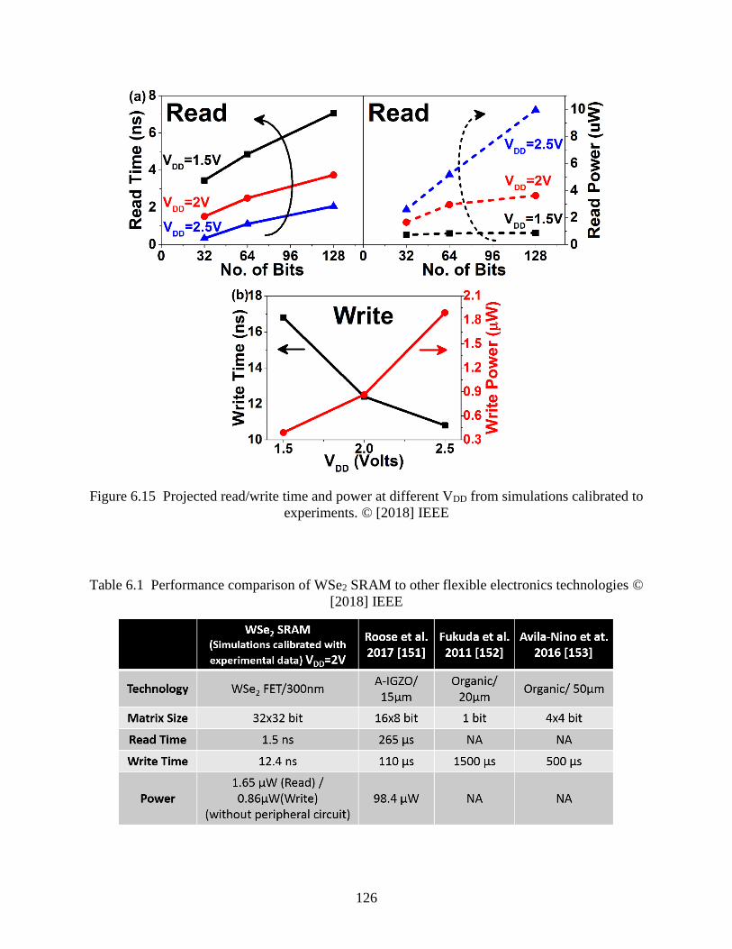
126
Figure 6.15 Projected read/write time and power at different VDD from simulations calibrated to
experiments. © [2018] IEEE
Table 6.1 Performance comparison of WSe2 SRAM to other flexible electronics technologies ©
[2018] IEEE

127
6.4 Conclusion
We have demonstrated WSe2 based CMOS inverters and CMOS SRAM for the first time
with comprehensive DC analyses. The tunability in inverter’s NM extends its potential for
applications with different demands on pull-up and pull-down capabilities. On the other hand,
combining tunable n-FETs with R/W assist techniques, stable SRAM operation at low VDD of 0.8V
is achieved. Superior speed and power compared to other technologies is predicted, suggesting a
promising application in flexible electronics and IoT.
128
STEEP SLOPE CNT TUNNELING FETS
7.1 CNT as a Candidate for TFET
The first experimental observation of this type of switching was succeeded by Appenzeller
et al. in 2004 through a dual-gated carbon nanotube (CNT) transistor [154]. Extensive research in
simulations and experiments of TFETs have been carried out since then for various channel
materials, device structures, and junction types (homo- and hetero-). However, although SSmin
below 60 mV/dec is observed, it is still a challenging endeavor to achieve a promising on-state
performance as predicted by simulations [155]–[160].
In this chapter, we present CNTFETs using a triple gate design to create an n-i-p
electrostatic doping profile, demonstrating room temperature TFET operation with SS less than
60mV/dec and a high tunneling current of ~ 10 μA/μm (normalized to a placement of targeted 100
CNTs within 1μm width [161]). Using CNTs as the channel material is beneficial to achieve steep
SS, owing to the fact that CNTs have ultra-small body thickness to achieve excellent electrostatic
control and suitable bandgap sizes with relatively small effective mass. Furthermore, quasi ballistic
transport has been demonstrated in one dimensional (1D) CNTs [162], which provides the
potential for ultimate on-state performance. For TFETs, on-state current critically depends on the
transmission probability, TWKB of the tunneling junction, which can be estimated through WKB
approximation as : [142], [143], [163]
TWKB ~
* 3/2
g
g
4λ 2m Eexp -
3q (E +ΔΦ)
(3-1)
Where m* is the effective mass, Eg is the band gap, ΔΦ is the energetic difference in the tunneling
window, and λ denotes as a characteristic length to describe the spatial extent in the p-n junction.
It is found that this approximation works properly for direct bandgap semiconductors [164], which
is the case for CNTs. For a planar gate structure as shown in Figure 1(a), the characteristic length
can be estimated by 𝜆 = √(ℇ𝑛𝑡
ℇ𝑜𝑥)𝑑𝑛𝑡𝑑𝑜𝑥 [56], [165], where ℇ𝑛𝑡 , ℇ𝑜𝑥 are the relative dielectric
constant for the CNT and gate oxide, respectively, and 𝑑𝑛𝑡, 𝑑𝑜𝑥are the diameter of CNT and the
oxide thickness. Using ultra-scaled gate dielectrics, 𝜆 can be very short since CNTs with relevant
bandgaps have diameters on the order of one nanometer, which will lead to large TWKB. Given the
129
natural cylindrical shape of 1D CNTs, gate-all-around geometry [166] can be employed to further
decrease the characteristic length following 2
nt nt ox nt oxλ= ε d ln(1+(2d /d ))/8ε [167], which will
further increase TWKB and achieve steep SS and high tunneling current. In most TFET designs,
degenerate doping in the source region is a common approach to create steep band bending for
efficient BTBT. However, chemical doping results in undesired band edge smearing with density
of states exponentially decaying into the bandgap, which may hinder sharp turn-on in TFET
operations and result in degraded SS [168], [169]. Therefore, we employ the triple gate design,
shown in Fig. 1(a) and (b) to achieve the desired electrostatic doping profile.
In the following sections, we first discuss the implementation of triple-gate CNT device in
section 7-2, followed by section 7-3 in analyzing an operation as a p-type MOSFET (PMOS) in
comparison with TFET under different gating scenario. SSmin < 60mV/dec is observed in the TFET
operation, and shows no temperature dependence as expected in section 7-4. In section 7-5, we
investigate the enhancement of the tunneling current through CNTs with smaller bandgaps. We
suggest that exploring materials with combination of a desired band gap and body thickness is
essential to achieve optimal TFET performance. Finally, we show output characteristics of the
device. In small VDS region, current increases linearly with the drain bias for PMOS owing to
negligible Schottky-barriers (SB) at the CNT and metal contact interface, while non-linear
behavior is observed for TFET due to possible drain-induced barrier thinning.
7.2 Device Implementation
Figure 7.1 (a) and (b) show a schematic and a scanning electron microscope (SEM) image
of an as-fabricated triple-gate device using palladium (Pd) source/drain (S/D) electrodes. A more
detailed process of fabrication is described in Figure 7.2. In our triple top gates design, similar to
section 5-3, the two side gates (TGS and TGD) are used to electrostatically gate the extended
source and drain regions (segments next to the source and drain). Depending on the magnitude and
polarity of the voltage applied on these two side-gate electrodes, the device can be configured to
operate as a PMOS with p-i-p doping profile or a TFET with n-i-p doping profile.
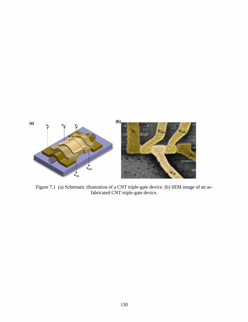
130
Figure 7.1 (a) Schematic illustration of a CNT triple-gate device. (b) SEM image of an as-
fabricated CNT triple-gate device.
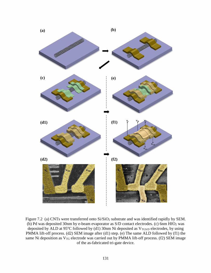
131
Figure 7.2 (a) CNTs were transferred onto Si/SiO2 substrate and was identified rapidly by SEM.
(b) Pd was deposited 30nm by e-beam evaporator as S/D contact electrodes. (c) 6nm HfO2 was
deposited by ALD at 95oC followed by (d1) 30nm Ni deposited as VTGS/D electrodes, by using
PMMA lift-off process. (d2) SEM image after (d1) step. (e) The same ALD followed by (f1) the
same Ni deposition as VTG electrode was carried out by PMMA lift-off process. (f2) SEM image
of the as-fabricated tri-gate device.
(d2)
(a) (b)
(c) (e)
(d1) (f1)
(f2)
132
7.3 PMOS/TFET Operation of Triple-gate CNT Device
Transfer characteristics as a function of the middle gate voltage, VTG, for five VTGS ranging
from -1.25V to +3V are presented in Figure 7.3(a). VTGD = -2V is applied to the segment next to
the drain so that it is heavily p-doped through the electrostatic gating, and VDS = -0.5V is applied
in favor of these holes to leave the drain. The negligible leakage indicated by the dotted lines is
attributed to good quality of dielectric from ALD and a small overlapping region between each
gate as revealed in the Figure 7.1(b). Figure 7.3(b) illustrates the corresponding band profiles at
rather negative VTG (Fermi level is in the valence band of the middle segment) for 5 curves from
Figure 7.3(a). Efs and Efd are Fermi levels in the source/drain. Eg is the bandgap with Ec and Ev
being the edge of the conduction band and valence band, respectively. At the on-state of the p-
branch (VTG <-1V), non-monotonic behaviors are observed when VTGS changes from negative to
positive. The band bending for the red curve measured with VTGS = -1.25V, VTG = -2V and VDS =
-0.5V is shown in case ○1 of Figure 7.3(b). PMOS operation with p+-i-p+ doping profile is created
and hole carrier injection from the source to the drain is expected. In case ○2 , fewer holes are
injected to the channel at VTGS = 0V, which results in a lower on-state current (orange curve) but
the same SS of ~ 80 mV/dec as in case ○1 owing to the thermionic current injection over the barrier
in both cases. It is observed that almost no carriers can be injected, hence very small currents are
measured (purple curve) when VTGS = +0.5V since Efs is aligned in the middle of the bandgap as
shown in case ○3 , in accordance with p-doping being removed from the extended source region.
When VTGS keeps being increased to be more positive, the CNT device finally enters the TFET
operation regime. As shown in case ○4 , with sufficiently positive VTGS being applied, the extended
source region is n-doped with electrons. At negative VTG, the middle channel region is aligned to
its valence band, hence, the electrons from the conduction band of the extended source region have
to tunnel to the valence band of the channel region, forming a BTBT current branch. Subsequently,
n-type electrostatics doping is further enhanced to n+ with VTGS = 3V in case ○5 , allowing higher
BTBT probability and observation of SSmin of ~ 41 mV/dec in the subthreshold regime. The reason
that SS of the BTBT branch becomes much smaller than 60 mV/dec at room temperature is due to
the bandpass-filter-like behavior of tunneling devices [142], [163]. As shown from case ○3 to ○5 ,
133
the band overlap in the source-channel only allows band to band carrier injection within a small,
gate-controlled energy window (case ○4 and ○5 ), with the high energy tail of the Fermi distribution
(light colored dashed line) being cut off by the bandgap of the channel region. This so-called
“effective cooling” renders SS much smaller than 60mV/dec even at room temperature. It also
raises an important requirement for the energy position of Efs respective to the edge of the
conduction band in the extended source region. Comparing case ○5 to ○4 , sufficient electrostatic
n-doping (basically n+) is necessary to allow more electrons to tunnel to the valence band to reach
a high BTBT on-state current, which is critical for observing steep SS in the device off-state
beyond the noise level of the measurements. Since air stable degenerate n-type chemical doping is
difficult to achieve in 1D CNTs, our triple top gate controlled electrostatic doping seems to be an
ideal solution for TFET operation that requires three independently controlled regions along the
channel. In the previously demonstrated CNT TFET operation [154], although the middle gate is
independently controlled, the common Si bottom gate used to control the extended source/drain
regions does not allow the formation of the n-i-p doping profile to achieve high performance BTBT
device operation. In addition, we have also tested triple gates with two local bottom gates
individually controlling the extended source/drain region and a top gate for the middle channel.
This design has never observed steep slopes despite decent current injection can be achieved. It is
suspected that due to the unavoidable overlap between the top and bottom gates, the band bending
at the tunneling junction is not efficiently controlled. These experimental results are provided in
Figure 7.4(a) to (c), with Efs and tunneling window being modulated by VBGS and VTG
simultaneously.
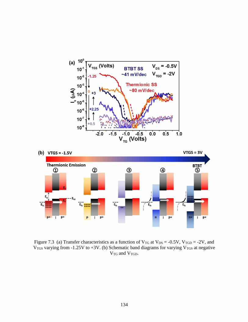
134
Figure 7.3 (a) Transfer characteristics as a function of VTG at VDS = -0.5V, VTGD = -2V, and
VTGS varying from -1.25V to +3V. (b) Schematic band diagrams for varying VTGS at negative
VTG and VTGD.
(a)
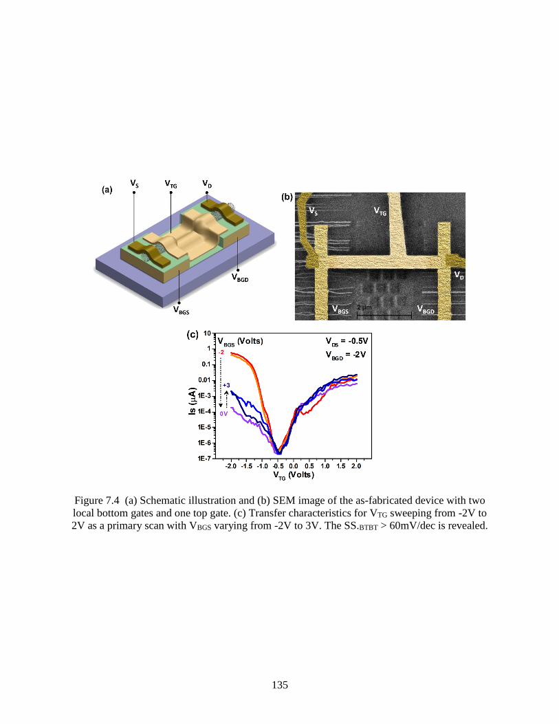
135
Figure 7.4 (a) Schematic illustration and (b) SEM image of the as-fabricated device with two
local bottom gates and one top gate. (c) Transfer characteristics for VTG sweeping from -2V to
2V as a primary scan with VBGS varying from -2V to 3V. The SS.BTBT > 60mV/dec is revealed.
136
7.4 Temperature-dependent Measurement
We then carry out measurements at various temperatures for the triple gate CNT devices
to verify the BTBT carrier transport. As has been reported in tunneling devices [154], [170]–[172],
lack of temperature dependence is an important feature of BTBT characteristics, which can be
distinguished from currents mediated by thermionic emission. Figure 7.5(a) compares transfer
characteristics at three different temperatures for the thermionic current injection of the PMOS
operation at VTGS = -2V and BTBT injection of the TFET operation at VTGS = +3V as we discussed
in Figure 7.3(a) and (b). The leakage current is below the noise level of our measurement system
indicated as the black curve, which will not impact the evaluation on the SS. The SS values at
different current levels are shown in Figure 7.5(b) for thermionic emission and BTBT. The SS for
the thermionic branch shows a typical temperature-dependent behevior given by SS =
ln10kT
q mV/dec (with Cox >> Cd + Cit) for any conventional MOSFET operation. On the other
hand, the SS of the BTBT branch shows no temperature dependence since the current injection is
controlled by the gate-modulated tunneling window instead of thermally broadened Fermi function.
We plot the distribution of SS extracted from cumulative measurements at different temperatures
as a function of current for these two different current injection mechanisms. Three observations
are clear and consistent with what we have stated above: (1) SS of BTBT is in general much lower
than that of the thermionic branch; SS < 60mV/dec at room temperature has been observed across
more than one order of magnitude current window, (2) Temperature independence is a
distinguishing feature of BTBT, (3) the BTBT currents are 2-3 orders of magnitude lower than the
thermionic currents. We will discuss what can be optimized in the device design to improve the
TFET’s on-state currents.
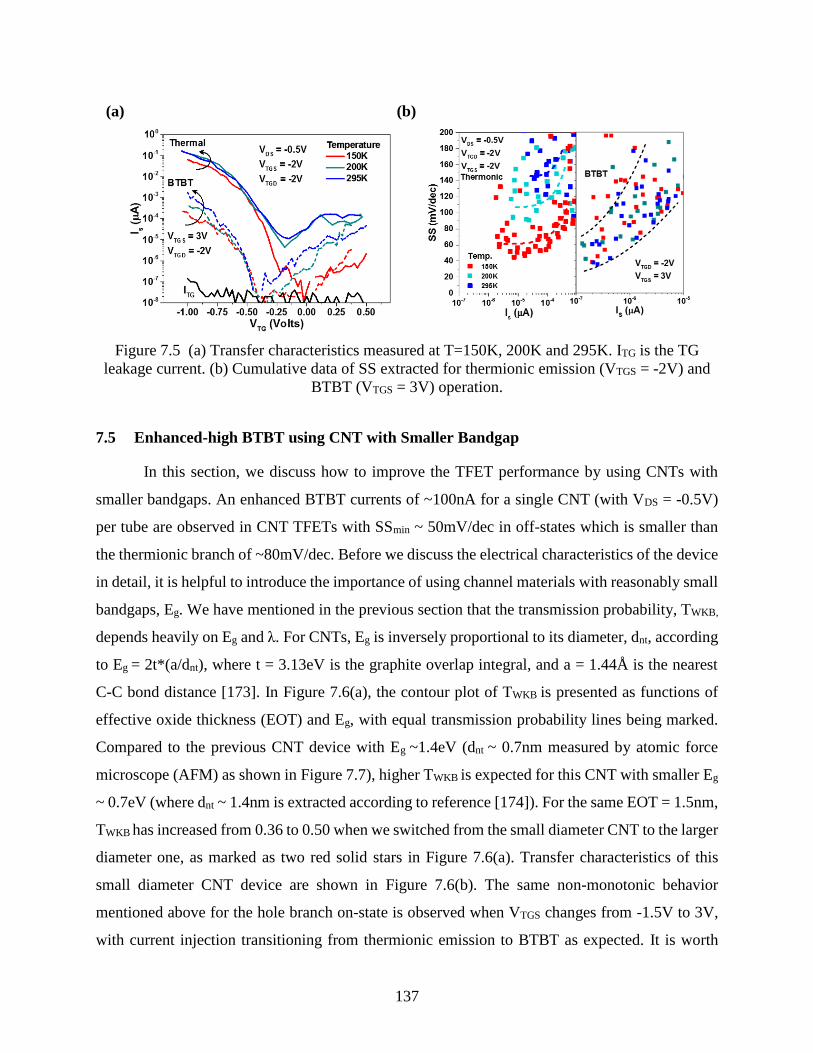
137
Figure 7.5 (a) Transfer characteristics measured at T=150K, 200K and 295K. ITG is the TG
leakage current. (b) Cumulative data of SS extracted for thermionic emission (VTGS = -2V) and
BTBT (VTGS = 3V) operation.
7.5 Enhanced-high BTBT using CNT with Smaller Bandgap
In this section, we discuss how to improve the TFET performance by using CNTs with
smaller bandgaps. An enhanced BTBT currents of ~100nA for a single CNT (with VDS = -0.5V)
per tube are observed in CNT TFETs with SSmin ~ 50mV/dec in off-states which is smaller than
the thermionic branch of ~80mV/dec. Before we discuss the electrical characteristics of the device
in detail, it is helpful to introduce the importance of using channel materials with reasonably small
bandgaps, Eg. We have mentioned in the previous section that the transmission probability, TWKB,
depends heavily on Eg and λ. For CNTs, Eg is inversely proportional to its diameter, dnt, according
to Eg = 2t*(a/dnt), where t = 3.13eV is the graphite overlap integral, and a = 1.44Å is the nearest
C-C bond distance [173]. In Figure 7.6(a), the contour plot of TWKB is presented as functions of
effective oxide thickness (EOT) and Eg, with equal transmission probability lines being marked.
Compared to the previous CNT device with Eg ~1.4eV (dnt ~ 0.7nm measured by atomic force
microscope (AFM) as shown in Figure 7.7), higher TWKB is expected for this CNT with smaller Eg
~ 0.7eV (where dnt ~ 1.4nm is extracted according to reference [174]). For the same EOT = 1.5nm,
TWKB has increased from 0.36 to 0.50 when we switched from the small diameter CNT to the larger
diameter one, as marked as two red solid stars in Figure 7.6(a). Transfer characteristics of this
small diameter CNT device are shown in Figure 7.6(b). The same non-monotonic behavior
mentioned above for the hole branch on-state is observed when VTGS changes from -1.5V to 3V,
with current injection transitioning from thermionic emission to BTBT as expected. It is worth
(a) (b)
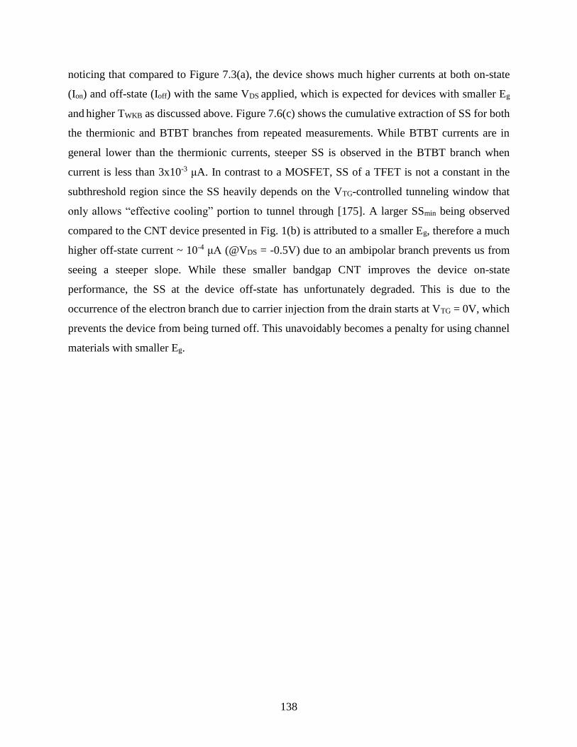
138
noticing that compared to Figure 7.3(a), the device shows much higher currents at both on-state
(Ion) and off-state (Ioff) with the same VDS applied, which is expected for devices with smaller Eg
and higher TWKB as discussed above. Figure 7.6(c) shows the cumulative extraction of SS for both
the thermionic and BTBT branches from repeated measurements. While BTBT currents are in
general lower than the thermionic currents, steeper SS is observed in the BTBT branch when
current is less than 3x10⁻³ μA. In contrast to a MOSFET, SS of a TFET is not a constant in the
subthreshold region since the SS heavily depends on the VTG-controlled tunneling window that
only allows “effective cooling” portion to tunnel through [175]. A larger SSmin being observed
compared to the CNT device presented in Fig. 1(b) is attributed to a smaller Eg, therefore a much
higher off-state current ~ 10-4 μA (@VDS = -0.5V) due to an ambipolar branch prevents us from
seeing a steeper slope. While these smaller bandgap CNT improves the device on-state
performance, the SS at the device off-state has unfortunately degraded. This is due to the
occurrence of the electron branch due to carrier injection from the drain starts at VTG = 0V, which
prevents the device from being turned off. This unavoidably becomes a penalty for using channel
materials with smaller Eg.
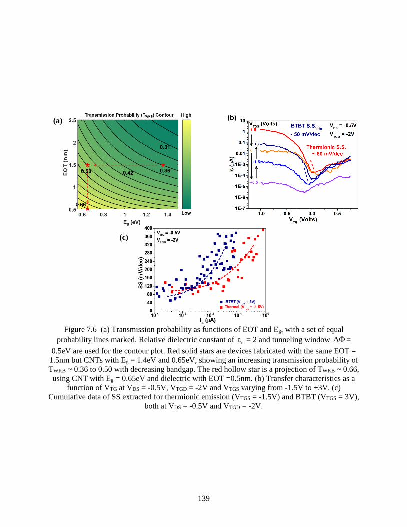
139
Figure 7.6 (a) Transmission probability as functions of EOT and Eg, with a set of equal
probability lines marked. Relative dielectric constant of ntε = 2 and tunneling window ΔΦ=
0.5eV are used for the contour plot. Red solid stars are devices fabricated with the same EOT =
1.5nm but CNTs with Eg = 1.4eV and 0.65eV, showing an increasing transmission probability of
TWKB ~ 0.36 to 0.50 with decreasing bandgap. The red hollow star is a projection of TWKB ~ 0.66,
using CNT with Eg = 0.65eV and dielectric with EOT =0.5nm. (b) Transfer characteristics as a
function of VTG at VDS = -0.5V, VTGD = -2V and VTGS varying from -1.5V to +3V. (c)
Cumulative data of SS extracted for thermionic emission (VTGS = -1.5V) and BTBT (VTGS = 3V),
both at VDS = -0.5V and VTGD = -2V.
(a)
(c)
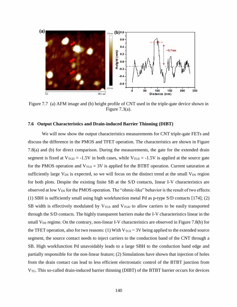
140
Figure 7.7 (a) AFM image and (b) height profile of CNT used in the triple-gate device shown in
Figure 7.3(a).
7.6 Output Characteristics and Drain-induced Barrier Thinning (DIBT)
We will now show the output characteristics measurements for CNT triple-gate FETs and
discuss the difference in the PMOS and TFET operation. The characteristics are shown in Figure
7.8(a) and (b) for direct comparison. During the measurements, the gate for the extended drain
segment is fixed at VTGD = -1.5V in both cases, while VTGS = -1.5V is applied at the source gate
for the PMOS operation and VTGS = 3V is applied for the BTBT operation. Current saturation at
sufficiently large VDS is expected, so we will focus on the distinct trend at the small VDS region
for both plots. Despite the existing finite SB at the S/D contacts, linear I-V characteristics are
observed at low VDS for the PMOS operation. The “ohmic-like” behavior is the result of two effects:
(1) SBH is sufficiently small using high workfunction metal Pd as p-type S/D contacts [174]; (2)
SB width is effectively modulated by VTGS and VTGD to allow carriers to be easily transported
through the S/D contacts. The highly transparent barriers make the I-V characteristics linear in the
small VDS regime. On the contrary, non-linear I-V characteristics are observed in Figure 7.8(b) for
the TFET operation, also for two reasons: (1) With VTGS = 3V being applied to the extended source
segment, the source contact needs to inject carriers to the conduction band of the CNT through a
SB. High workfunction Pd unavoidably leads to a large SBH to the conduction band edge and
partially responsible for the non-linear feature; (2) Simulations have shown that injection of holes
from the drain contact can lead to less efficient electrostatic control of the BTBT junction from
VTG. This so-called drain-induced barrier thinning (DIBT) of the BTBT barrier occurs for devices
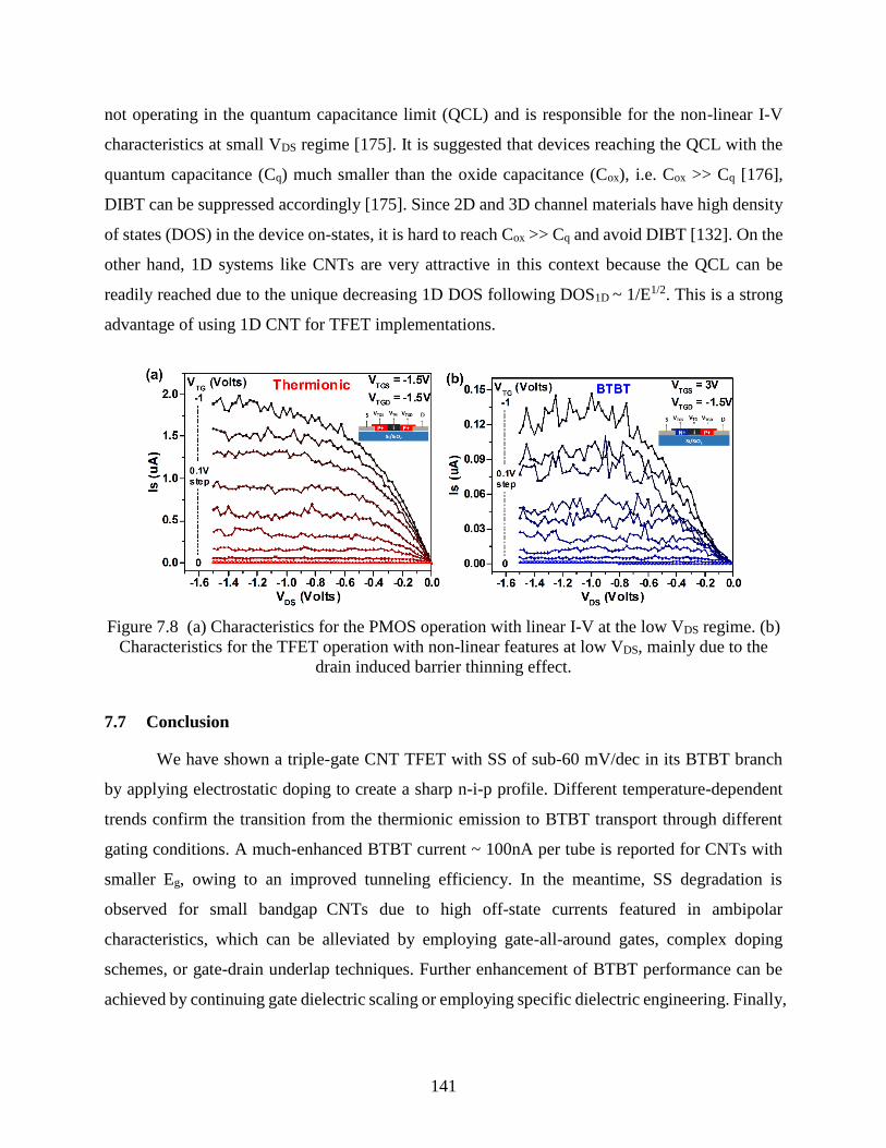
141
not operating in the quantum capacitance limit (QCL) and is responsible for the non-linear I-V
characteristics at small VDS regime [175]. It is suggested that devices reaching the QCL with the
quantum capacitance (Cq) much smaller than the oxide capacitance (Cox), i.e. Cox >> Cq [176],
DIBT can be suppressed accordingly [175]. Since 2D and 3D channel materials have high density
of states (DOS) in the device on-states, it is hard to reach Cox >> Cq and avoid DIBT [132]. On the
other hand, 1D systems like CNTs are very attractive in this context because the QCL can be
readily reached due to the unique decreasing 1D DOS following DOS1D ~ 1/E1/2. This is a strong
advantage of using 1D CNT for TFET implementations.
Figure 7.8 (a) Characteristics for the PMOS operation with linear I-V at the low VDS regime. (b)
Characteristics for the TFET operation with non-linear features at low VDS, mainly due to the
drain induced barrier thinning effect.
7.7 Conclusion
We have shown a triple-gate CNT TFET with SS of sub-60 mV/dec in its BTBT branch
by applying electrostatic doping to create a sharp n-i-p profile. Different temperature-dependent
trends confirm the transition from the thermionic emission to BTBT transport through different
gating conditions. A much-enhanced BTBT current ~ 100nA per tube is reported for CNTs with
smaller Eg, owing to an improved tunneling efficiency. In the meantime, SS degradation is
observed for small bandgap CNTs due to high off-state currents featured in ambipolar
characteristics, which can be alleviated by employing gate-all-around gates, complex doping
schemes, or gate-drain underlap techniques. Further enhancement of BTBT performance can be
achieved by continuing gate dielectric scaling or employing specific dielectric engineering. Finally,

142
we discussed the non-linear output characteristics observed in TFET operations and argue that 1D
CNT is the optimal channel material to overcome the DIBT by operating in the QCL.
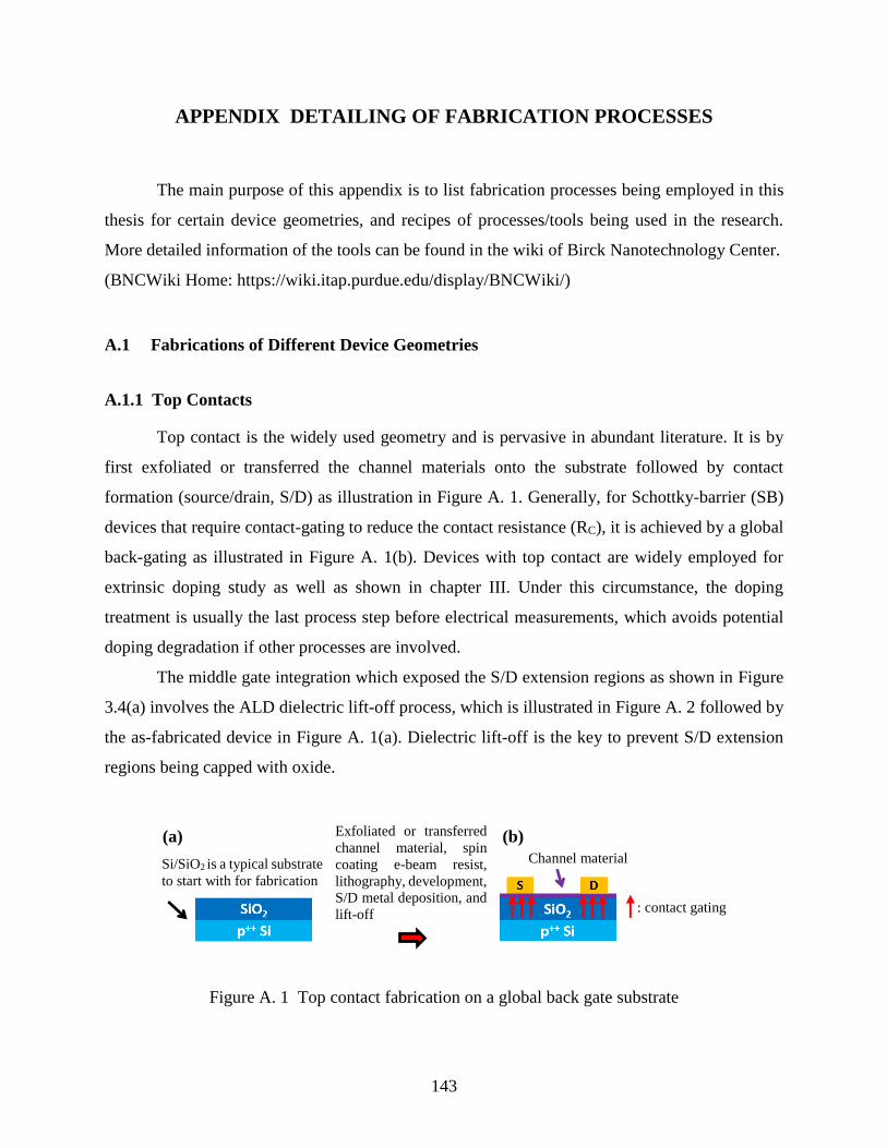
143
APPENDIX DETAILING OF FABRICATION PROCESSES
The main purpose of this appendix is to list fabrication processes being employed in this
thesis for certain device geometries, and recipes of processes/tools being used in the research.
More detailed information of the tools can be found in the wiki of Birck Nanotechnology Center.
(BNCWiki Home: https://wiki.itap.purdue.edu/display/BNCWiki/)
A.1 Fabrications of Different Device Geometries
A.1.1 Top Contacts
Top contact is the widely used geometry and is pervasive in abundant literature. It is by
first exfoliated or transferred the channel materials onto the substrate followed by contact
formation (source/drain, S/D) as illustration in Figure A. 1. Generally, for Schottky-barrier (SB)
devices that require contact-gating to reduce the contact resistance (RC), it is achieved by a global
back-gating as illustrated in Figure A. 1(b). Devices with top contact are widely employed for
extrinsic doping study as well as shown in chapter III. Under this circumstance, the doping
treatment is usually the last process step before electrical measurements, which avoids potential
doping degradation if other processes are involved.
The middle gate integration which exposed the S/D extension regions as shown in Figure
3.4(a) involves the ALD dielectric lift-off process, which is illustrated in Figure A. 2 followed by
the as-fabricated device in Figure A. 1(a). Dielectric lift-off is the key to prevent S/D extension
regions being capped with oxide.
Figure A. 1 Top contact fabrication on a global back gate substrate
Si/SiO2 is a typical substrate
to start with for fabrication
Exfoliated or transferred
channel material, spin
coating e-beam resist,
lithography, development,
S/D metal deposition, and
lift-off : contact gating
Channel material
(a) (b)
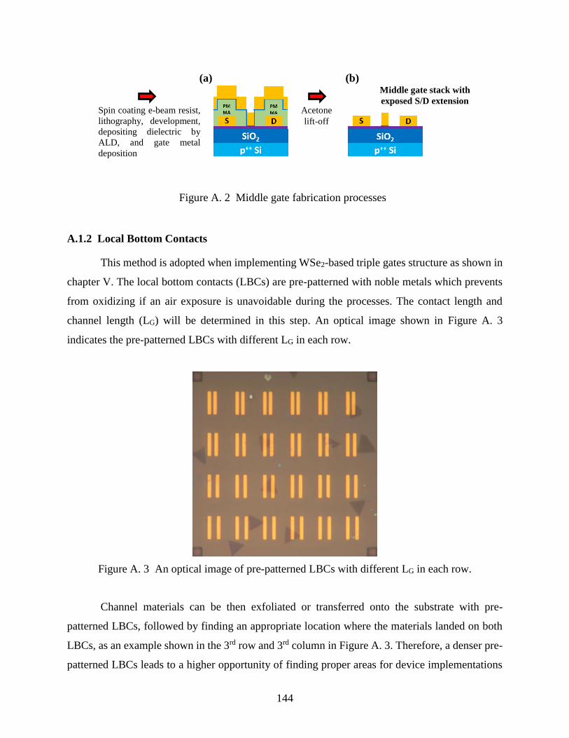
144
A.1.2 Local Bottom Contacts
This method is adopted when implementing WSe2-based triple gates structure as shown in
chapter V. The local bottom contacts (LBCs) are pre-patterned with noble metals which prevents
from oxidizing if an air exposure is unavoidable during the processes. The contact length and
channel length (LG) will be determined in this step. An optical image shown in Figure A. 3
indicates the pre-patterned LBCs with different LG in each row.
Figure A. 3 An optical image of pre-patterned LBCs with different LG in each row.
Channel materials can be then exfoliated or transferred onto the substrate with pre-
patterned LBCs, followed by finding an appropriate location where the materials landed on both
LBCs, as an example shown in the 3rd row and 3rd column in Figure A. 3. Therefore, a denser pre-
patterned LBCs leads to a higher opportunity of finding proper areas for device implementations
(b) (a)
Spin coating e-beam resist,
lithography, development,
depositing dielectric by
ALD, and gate metal
deposition
Acetone
lift-off
Middle gate stack with
exposed S/D extension
Figure A. 2 Middle gate fabrication processes
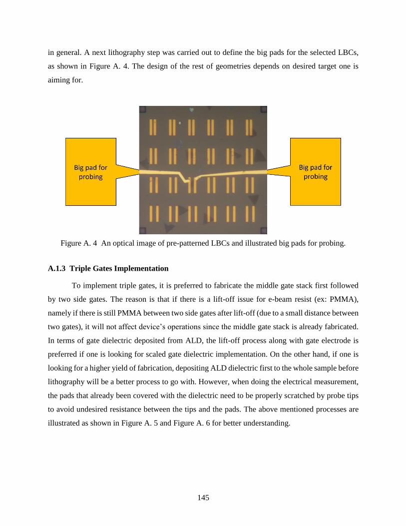
145
in general. A next lithography step was carried out to define the big pads for the selected LBCs,
as shown in Figure A. 4. The design of the rest of geometries depends on desired target one is
aiming for.
Figure A. 4 An optical image of pre-patterned LBCs and illustrated big pads for probing.
A.1.3 Triple Gates Implementation
To implement triple gates, it is preferred to fabricate the middle gate stack first followed
by two side gates. The reason is that if there is a lift-off issue for e-beam resist (ex: PMMA),
namely if there is still PMMA between two side gates after lift-off (due to a small distance between
two gates), it will not affect device’s operations since the middle gate stack is already fabricated.
In terms of gate dielectric deposited from ALD, the lift-off process along with gate electrode is
preferred if one is looking for scaled gate dielectric implementation. On the other hand, if one is
looking for a higher yield of fabrication, depositing ALD dielectric first to the whole sample before
lithography will be a better process to go with. However, when doing the electrical measurement,
the pads that already been covered with the dielectric need to be properly scratched by probe tips
to avoid undesired resistance between the tips and the pads. The above mentioned processes are
illustrated as shown in Figure A. 5 and Figure A. 6 for better understanding.
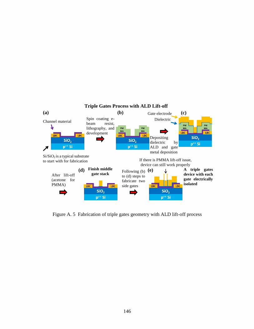
146
Figure A. 5 Fabrication of triple gates geometry with ALD lift-off process
Spin coating e-
beam resist,
lithography, and
development
Si/SiO2 is a typical substrate
to start with for fabrication
Channel material
Gate electrode
Dielectric
Depositing
dielectric by
ALD and gate
metal deposition
After lift-off
(acetone for
PMMA)
Finish middle
gate stack Following (b)
to (d) steps to
fabricate two
side gates
A triple gates
device with each
gate electrically
isolated
If there is PMMA lift-off issue,
device can still work properly
Triple Gates Process with ALD Lift-off
(a) (b) (c)
(d) (e)
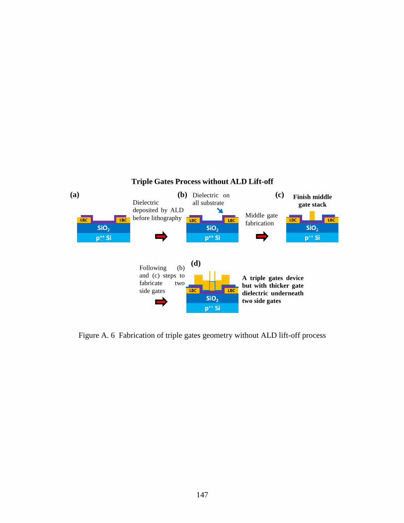
147
Figure A. 6 Fabrication of triple gates geometry without ALD lift-off process
Middle gate
fabrication
Dielectric
deposited by ALD
before lithography
Finish middle
gate stack
Dielectric on
all substrate
Following (b)
and (c) steps to
fabricate two
side gates
A triple gates device
but with thicker gate
dielectric underneath
two side gates
Triple Gates Process without ALD Lift-off
(a) (b) (c)
(d)
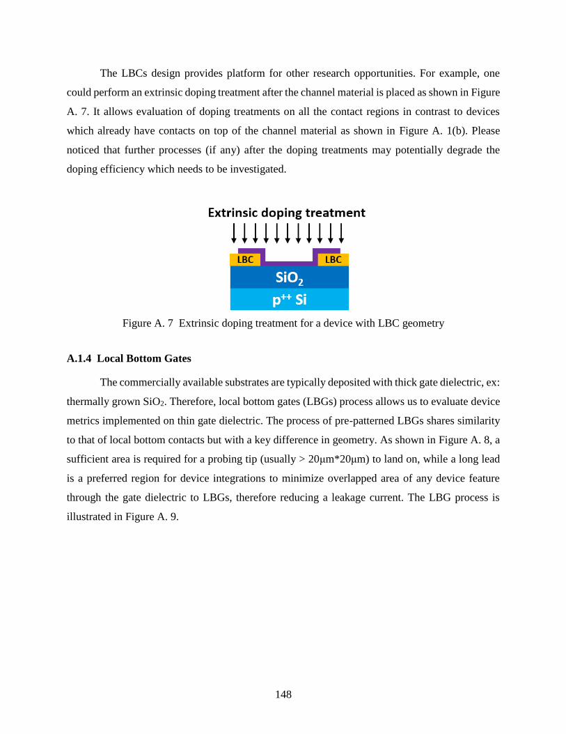
148
The LBCs design provides platform for other research opportunities. For example, one
could perform an extrinsic doping treatment after the channel material is placed as shown in Figure
A. 7. It allows evaluation of doping treatments on all the contact regions in contrast to devices
which already have contacts on top of the channel material as shown in Figure A. 1(b). Please
noticed that further processes (if any) after the doping treatments may potentially degrade the
doping efficiency which needs to be investigated.
Figure A. 7 Extrinsic doping treatment for a device with LBC geometry
A.1.4 Local Bottom Gates
The commercially available substrates are typically deposited with thick gate dielectric, ex:
thermally grown SiO2. Therefore, local bottom gates (LBGs) process allows us to evaluate device
metrics implemented on thin gate dielectric. The process of pre-patterned LBGs shares similarity
to that of local bottom contacts but with a key difference in geometry. As shown in Figure A. 8, a
sufficient area is required for a probing tip (usually > 20μm*20μm) to land on, while a long lead
is a preferred region for device integrations to minimize overlapped area of any device feature
through the gate dielectric to LBGs, therefore reducing a leakage current. The LBG process is
illustrated in Figure A. 9.
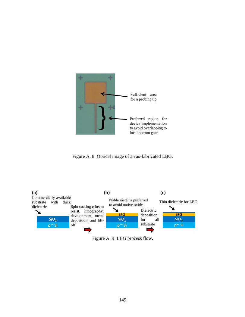
149
Figure A. 8 Optical image of an as-fabricated LBG.
Figure A. 9 LBG process flow.
Preferred region for
device implementation
to avoid overlapping to
local bottom gate
Sufficient area
for a probing tip
}
Dielectric
deposition
for all
substrate
Spin coating e-beam
resist, lithography,
development, metal
deposition, and lift-
off
Commercially available
substrate with thick
dielectric
Noble metal is preferred
to avoid native oxide Thin dielectric for LBG
(a) (b) (c)
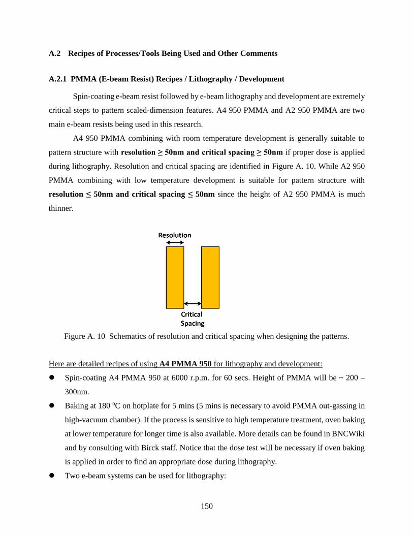
150
A.2 Recipes of Processes/Tools Being Used and Other Comments
A.2.1 PMMA (E-beam Resist) Recipes / Lithography / Development
Spin-coating e-beam resist followed by e-beam lithography and development are extremely
critical steps to pattern scaled-dimension features. A4 950 PMMA and A2 950 PMMA are two
main e-beam resists being used in this research.
A4 950 PMMA combining with room temperature development is generally suitable to
pattern structure with resolution ≥ 50nm and critical spacing ≥ 50nm if proper dose is applied
during lithography. Resolution and critical spacing are identified in Figure A. 10. While A2 950
PMMA combining with low temperature development is suitable for pattern structure with
resolution ≤ 50nm and critical spacing ≤ 50nm since the height of A2 950 PMMA is much
thinner.
Figure A. 10 Schematics of resolution and critical spacing when designing the patterns.
Here are detailed recipes of using A4 PMMA 950 for lithography and development:
Spin-coating A4 PMMA 950 at 6000 r.p.m. for 60 secs. Height of PMMA will be ~ 200 –
300nm.
Baking at 180 oC on hotplate for 5 mins (5 mins is necessary to avoid PMMA out-gassing in
high-vacuum chamber). If the process is sensitive to high temperature treatment, oven baking
at lower temperature for longer time is also available. More details can be found in BNCWiki
and by consulting with Birck staff. Notice that the dose test will be necessary if oven baking
is applied in order to find an appropriate dose during lithography.
Two e-beam systems can be used for lithography:

151
1. Raith: It could offer up to 30 keV e-beam for pattern writing. A typical dose for fine
features (resolution ≤ 1μm in general) is ~ 200 (μC/cm2) with 10μm aperture at 20 keV,
while a typical dose for big features is ~ 160 (μC/cm2) with 60μm aperture at 20 keV.
2. JEOL: It provides 100 keV e-beam for pattern writing, which could achieve a faster
writing speed and better resolution (less electron back-scattering). A typical dose is base
dose ~ 600 (μC/cm2) with proximity-effect-correct (PEC) for A4 PMMA 950 being
applied. Notice that using PEC is very critical since over-exposure is expected if PEC is
not applied, as shown in Figure A. 11.
(E-beam recipe is by courtesy of Peng Wu and image of Figure A. 11 is by courtesy of
Chin-Cheng Chiang).
Preparing two beakers. One with IPA/Water = 3/1 (typically 60ml of IPA and 20ml of water).
Another with pure IPA. Dip the sample into IPA/Water for 60 secs followed by IPA dipping
for 10 secs. N2 gun blowing for at least 30 secs to make sure no solution left behind in the
developed patterns. (If working with very fine features with an extreme resolution, blowing
for 2 mins is recommended)
Checking the patterns with an optical microscope before next processes.
Here are detailed recipes of using A2 PMMA 950 for lithography and development:
Spin-coating A2 PMMA 950 at 6000 r.p.m. for 60 secs. Height of PMMA will be ~ 80 -
100nm.
Baking at 180 oC on hotplate for 5 mins (5 mins is necessary to avoid PMMA out-gassing in
high-vacuum chamber). If the process is sensitive to high temperature treatment, oven baking
at lower temperature for longer time is also available. More details can be find in BNCWiki
and by consulting with Birck staff. Notice that the dose test will be necessary if oven baking
is applied in order to find an appropriate dose during lithography.
Only JEOL is tried out by the author for lithography:
1. JEOL: It provides 100 keV e-beam for pattern writing, which could achieve a faster
writing speed and better resolution (less electron back-scattering). A typical dose is base
dose ~ 1400 (μC/cm2) with proximity-effect-correct (PEC) for A2 PMMA 950 being
applied. Notice that using PEC is very critical especially for designed with resolution ≤
50nm and critical spacing ≤ 50nm.
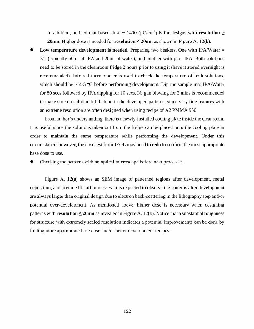
152
In addition, noticed that based dose ~ 1400 (μC/cm2) is for designs with resolution ≥
20nm. Higher dose is needed for resolution ≤ 20nm as shown in Figure A. 12(b).
Low temperature development is needed. Preparing two beakers. One with IPA/Water =
3/1 (typically 60ml of IPA and 20ml of water), and another with pure IPA. Both solutions
need to be stored in the cleanroom fridge 2 hours prior to using it (have it stored overnight is
recommended). Infrared thermometer is used to check the temperature of both solutions,
which should be ~ 4-5 oC before performing development. Dip the sample into IPA/Water
for 80 secs followed by IPA dipping for 10 secs. N2 gun blowing for 2 mins is recommended
to make sure no solution left behind in the developed patterns, since very fine features with
an extreme resolution are often designed when using recipe of A2 PMMA 950.
From author’s understanding, there is a newly-installed cooling plate inside the cleanroom.
It is useful since the solutions taken out from the fridge can be placed onto the cooling plate in
order to maintain the same temperature while performing the development. Under this
circumstance, however, the dose test from JEOL may need to redo to confirm the most appropriate
base dose to use.
Checking the patterns with an optical microscope before next processes.
Figure A. 12(a) shows an SEM image of patterned regions after development, metal
deposition, and acetone lift-off processes. It is expected to observe the patterns after development
are always larger than original design due to electron back-scattering in the lithography step and/or
potential over-development. As mentioned above, higher dose is necessary when designing
patterns with resolution ≤ 20nm as revealed in Figure A. 12(b). Notice that a substantial roughness
for structure with extremely scaled resolution indicates a potential improvements can be done by
finding more appropriate base dose and/or better development recipes.
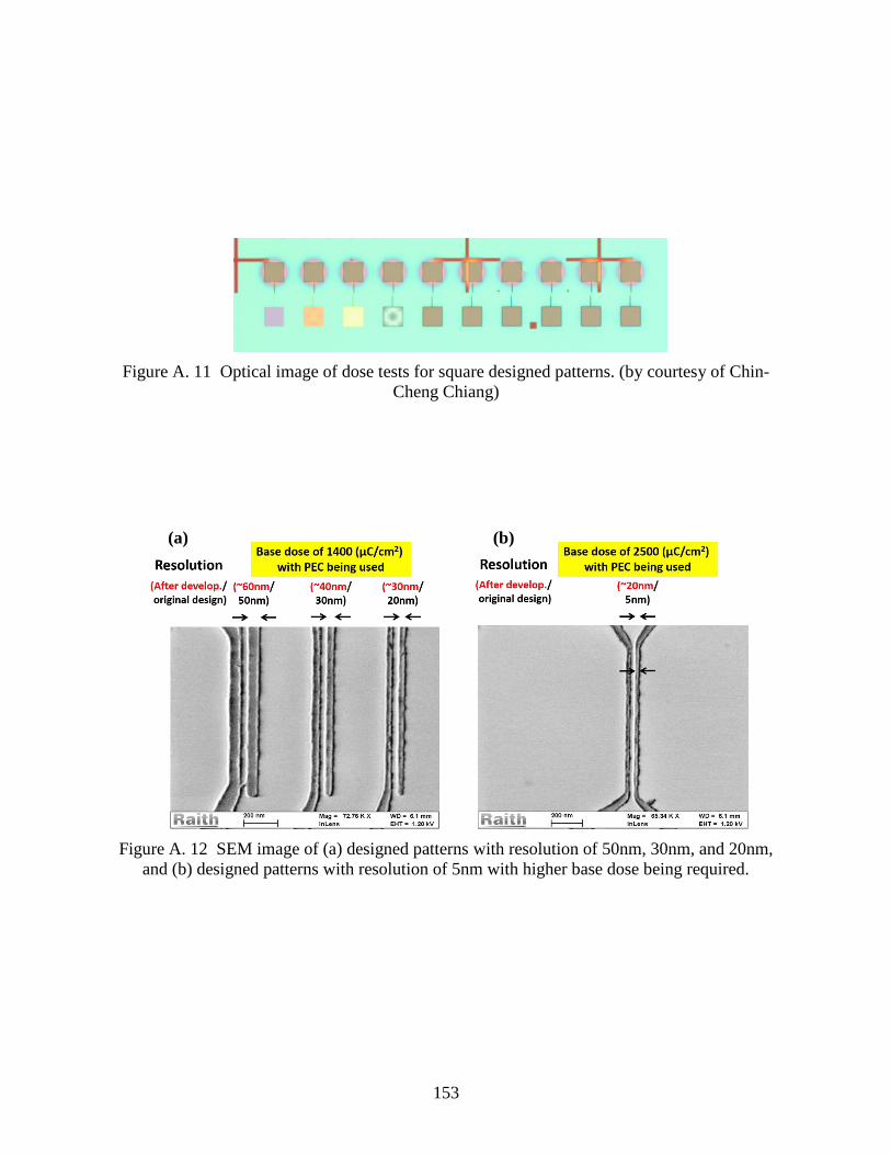
153
Figure A. 11 Optical image of dose tests for square designed patterns. (by courtesy of Chin-
Cheng Chiang)
Figure A. 12 SEM image of (a) designed patterns with resolution of 50nm, 30nm, and 20nm,
and (b) designed patterns with resolution of 5nm with higher base dose being required.
(a) (b)

154
Additional Comments
Since the height of A2 PMMA 950 is only ~ 80 – 100nm, the thickness of metal deposition
can’t be too large if lift-off process will be applied. From author’s experience, depositing
metal with 60nm still works well in terms of successful lift-off and high yield. Although metal
thickness > 60nm has not been tried out by the author yet, it is recommended if it still work
since it could further reduce extrinsic metal line resistances.
Image of dose test to reveal over-exposure and under-exposure after development is shown
in Figure A. 11 examined by an optical microscope (by courtesy of Chin-Cheng Chiang). All
features in 1st row are over-exposed from JEOL e-beam system since PEC is not applied. 1st
to 4th column in 2nd row are under-exposed with applied dose being too low so the features
can’t be fully developed. The features in column 5th and 6th in 2nd row are having appropriate
based dose and PEC being applied followed by an appropriate development process, so the
features are very square in accordance to the design. With larger dose being applied, i.e. 10th
column in 2nd row, the edges of the square start to expand and the overall feature starts to
become rounded, indicating a slight over-exposure during lithography.
To identify if over-development occurs, one could observe the edge of the feature after
development. As shown in Figure A. 13(a), the “double-line” feature indicates potential over-
development as illustrated in Figure A. 13(c), since both edges of PMMA are visible
observing from the top. The ideal feature after development is illustrated in Figure A. 13(b)
when proper dose for lithography and proper time for development are both achieved. A
slightly over-development is not a big issue since under-development will result in PMMA
residues which is even more undesired. However, substantial over-development will lead to
a lift-off issue especially for features with small spacing.
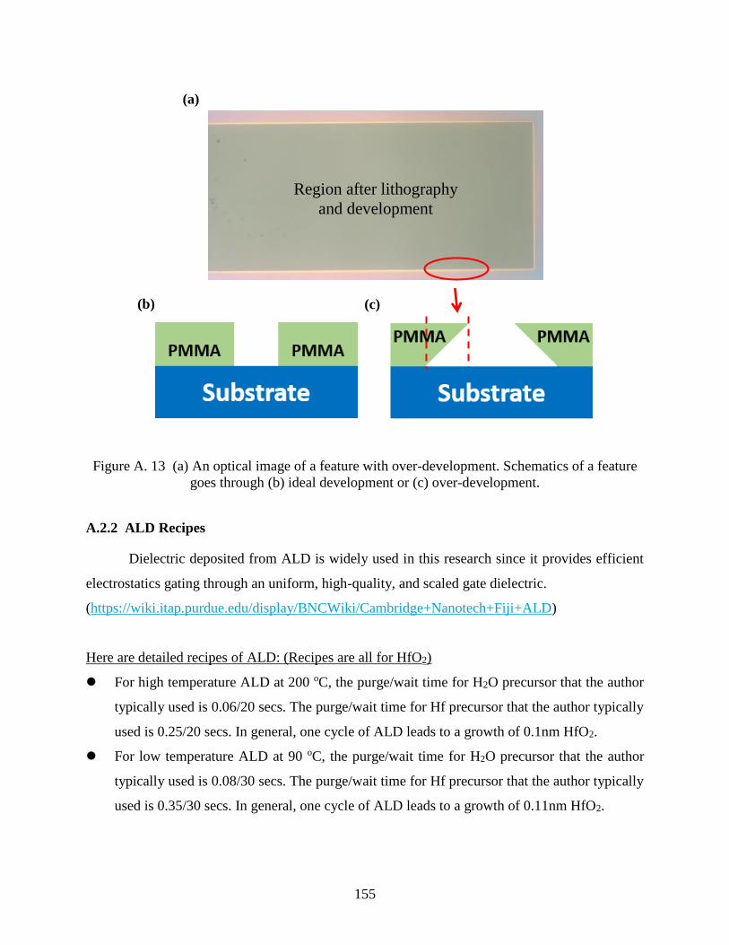
155
Figure A. 13 (a) An optical image of a feature with over-development. Schematics of a feature
goes through (b) ideal development or (c) over-development.
A.2.2 ALD Recipes
Dielectric deposited from ALD is widely used in this research since it provides efficient
electrostatics gating through an uniform, high-quality, and scaled gate dielectric.
(https://wiki.itap.purdue.edu/display/BNCWiki/Cambridge+Nanotech+Fiji+ALD)
Here are detailed recipes of ALD: (Recipes are all for HfO2)
For high temperature ALD at 200 oC, the purge/wait time for H2O precursor that the author
typically used is 0.06/20 secs. The purge/wait time for Hf precursor that the author typically
used is 0.25/20 secs. In general, one cycle of ALD leads to a growth of 0.1nm HfO2.
For low temperature ALD at 90 oC, the purge/wait time for H2O precursor that the author
typically used is 0.08/30 secs. The purge/wait time for Hf precursor that the author typically
used is 0.35/30 secs. In general, one cycle of ALD leads to a growth of 0.11nm HfO2.
(b)
(a)
(c)
Region after lithography
and development

156
Additional Comments
Please consult with colleagues for the archive recipe that the group members typically used.
It contains noble gas flow rate that we will not adjust.
Without surface treratments/functionalizations, Al seeding layer of ~ 1nm is usually
deposited from PVD with extremely slow rate prior to ALD. The ultra-thin Al seeding layer
can form into Al2O3 with air-exposure for ~ 10 mins.
ALD lift-off process is described in Figure A. 2 and Figure A. 5. Normally, the ALD lift-off
is considered harder than merely metal lift-off, especially for features with small resolution
and scaled spacing. It is due to a conformal coverage of ALD instead of directional deposition
of metals from an e-beam evaporator. Nonetheless, with proper lithography, development,
and lift-off, one can still expect a high yield of device fabrications.
A dummy ALD process ( ~ 5 cycles) is recommended prior to putting the sample into the
chamber. The dummy process makes sure the precursors of H2O and Hf work well by
observing the pressure values and by comparing that with the records in the excel file from
previous users.
For ALD lift-off, double PMMA layers are encouraged to improve the fabrication yield. Here
is the recipe the author had tried out. Spin-coating A4 PMMA 495 at 6000 r.p.m. for 60 secs,
followed by baking on the hotplate for 5 mins. Then, spin-coating A4 PMMA 950 at 6000
r.p.m. for 60 secs, followed by baking on the hotplate for 5 mins.
Only Raith is tried out for lithography by the author for double-layered PMMA:
A typical dose for fine features (resolution ≤ 1μm in general) is ~ 240 (μC/cm2) with 10μm
aperture at 20 keV, while a typical dose for big features is ~ 200 (μC/cm2) with 60μm aperture
at 20 keV. It is not surprised that the dose is higher than that in single A4 PMMA 950 since
the overall thickness of double-layered PMMA is thicker.
A.2.3 SiNx N-doping
As discussed in section 3-2, the n-doping is attributed to silicon nitride grown by plasma-
enhanced CVD contains a high density of positive charge centers originating from +Si≡N3
dangling bonds known as K+ centers [78].

157
Here are detailed recipes of SiNx passivation:
Axic PECVD is used to deposit SiNx. The flow rates of silane SiH4 / ammonia NH3 is 100 /
30 sccm to create a non-stoichiometry nitride film which bears positive charge centers that is
suggested in [78]. The deposition power is 50W, temperature is 150 oC, chamber pressure is
900 mTorr, chuck spacing is 3”, and the deposition time is 6 mins.
(https://wiki.itap.purdue.edu/display/BNCWiki/Axic+PECVD)
Additional Comments
From author’s experience, this process is compatible with lift-off process. However, the
doping strength is compromised after solution processes based on author’s observation.
(Since the sample needs to be put into acetone for a least 1 hour to complete lift-off process)
Based on results from author’s colleague, if the SiNx is not thick enough, there will be no
doping effect. Therefore, a SiNx thickness-dependent doping strength is expected which is
not the focus in this research yet.
Modifying the ratio of silane (SiH4) / ammonia (NH3) flow rates leads to different doping
strength according to [78].
If lift-off process is not used, the thick SiNx will be passivated on all the sample. Therefore,
scratching from probe tips to big pads is necessary. Based on author’s experience, since the
device yield after SiNx passivation is not degraded, if weird electrical curves are measured, it
is very likely due to huge resistances associated with probe tips and big pads from a non-fully
scratching.
A.2.4 Nitric Oxide Annealing P-doping
As discussed in section 3-4, nitric oxide annealing on WSe2 results in a significant p-doping
effect, with high hole current and ultra-low RC being observed. The system being used is Nitric
Oxide Anneal
(https://wiki.itap.purdue.edu/display/BNCWiki/Nitric+Oxide+Anneal).

158
Here are detailed recipes of nitric oxide annealing p-doping:
Sample is put on the quartz boat and delivered toward the center of the tube. Keeping the Ar
flow while setting to a desired temperature. Once the temperature has reached the set value,
wait ~ 5 mins for stabilization. Then, turn off the Ar flow and turn on the nitric oxide gas.
Since nitric oxide is a toxic gas, please have it well-trained by the Birck staff before
performing research.
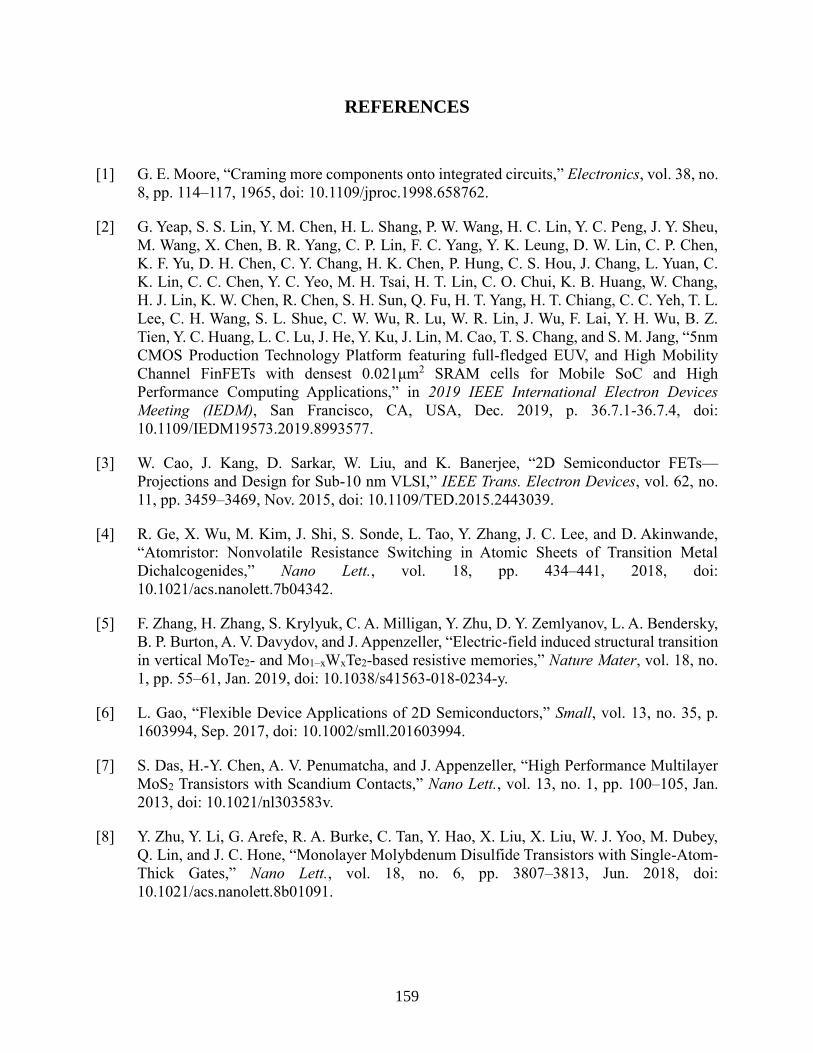
159
REFERENCES
[1] G. E. Moore, “Craming more components onto integrated circuits,” Electronics, vol. 38, no.
8, pp. 114–117, 1965, doi: 10.1109/jproc.1998.658762.
[2] G. Yeap, S. S. Lin, Y. M. Chen, H. L. Shang, P. W. Wang, H. C. Lin, Y. C. Peng, J. Y. Sheu,
M. Wang, X. Chen, B. R. Yang, C. P. Lin, F. C. Yang, Y. K. Leung, D. W. Lin, C. P. Chen,
K. F. Yu, D. H. Chen, C. Y. Chang, H. K. Chen, P. Hung, C. S. Hou, J. Chang, L. Yuan, C.
K. Lin, C. C. Chen, Y. C. Yeo, M. H. Tsai, H. T. Lin, C. O. Chui, K. B. Huang, W. Chang,
H. J. Lin, K. W. Chen, R. Chen, S. H. Sun, Q. Fu, H. T. Yang, H. T. Chiang, C. C. Yeh, T. L.
Lee, C. H. Wang, S. L. Shue, C. W. Wu, R. Lu, W. R. Lin, J. Wu, F. Lai, Y. H. Wu, B. Z.
Tien, Y. C. Huang, L. C. Lu, J. He, Y. Ku, J. Lin, M. Cao, T. S. Chang, and S. M. Jang, “5nm
CMOS Production Technology Platform featuring full-fledged EUV, and High Mobility
Channel FinFETs with densest 0.021μm2 SRAM cells for Mobile SoC and High
Performance Computing Applications,” in 2019 IEEE International Electron Devices
Meeting (IEDM), San Francisco, CA, USA, Dec. 2019, p. 36.7.1-36.7.4, doi:
10.1109/IEDM19573.2019.8993577.
[3] W. Cao, J. Kang, D. Sarkar, W. Liu, and K. Banerjee, “2D Semiconductor FETs—
Projections and Design for Sub-10 nm VLSI,” IEEE Trans. Electron Devices, vol. 62, no.
11, pp. 3459–3469, Nov. 2015, doi: 10.1109/TED.2015.2443039.
[4] R. Ge, X. Wu, M. Kim, J. Shi, S. Sonde, L. Tao, Y. Zhang, J. C. Lee, and D. Akinwande,
“Atomristor: Nonvolatile Resistance Switching in Atomic Sheets of Transition Metal
Dichalcogenides,” Nano Lett., vol. 18, pp. 434–441, 2018, doi:
10.1021/acs.nanolett.7b04342.
[5] F. Zhang, H. Zhang, S. Krylyuk, C. A. Milligan, Y. Zhu, D. Y. Zemlyanov, L. A. Bendersky,
B. P. Burton, A. V. Davydov, and J. Appenzeller, “Electric-field induced structural transition
in vertical MoTe2- and Mo1–xWxTe2-based resistive memories,” Nature Mater, vol. 18, no.
1, pp. 55–61, Jan. 2019, doi: 10.1038/s41563-018-0234-y.
[6] L. Gao, “Flexible Device Applications of 2D Semiconductors,” Small, vol. 13, no. 35, p.
1603994, Sep. 2017, doi: 10.1002/smll.201603994.
[7] S. Das, H.-Y. Chen, A. V. Penumatcha, and J. Appenzeller, “High Performance Multilayer
MoS2 Transistors with Scandium Contacts,” Nano Lett., vol. 13, no. 1, pp. 100–105, Jan.
2013, doi: 10.1021/nl303583v.
[8] Y. Zhu, Y. Li, G. Arefe, R. A. Burke, C. Tan, Y. Hao, X. Liu, X. Liu, W. J. Yoo, M. Dubey,
Q. Lin, and J. C. Hone, “Monolayer Molybdenum Disulfide Transistors with Single-Atom-
Thick Gates,” Nano Lett., vol. 18, no. 6, pp. 3807–3813, Jun. 2018, doi:
10.1021/acs.nanolett.8b01091.
160
[9] A. Nourbakhsh, A. Zubair, R. N. Sajjad, A. Tavakkoli K. G., W. Chen, S. Fang, X. Ling, J.
Kong, M. S. Dresselhaus, E. Kaxiras, K. K. Berggren, D. Antoniadis, and T. Palacios, “MoS2
Field-Effect Transistor with Sub-10 nm Channel Length,” Nano Lett., vol. 16, no. 12, pp.
7798–7806, Dec. 2016, doi: 10.1021/acs.nanolett.6b03999.
[10] Y. Liu, J. Guo, Y. Wu, E. Zhu, N. O. Weiss, Q. He, H. Wu, H.-C. Cheng, Y. Xu, I. Shakir, Y.
Huang, and X. Duan, “Pushing the Performance Limit of Sub-100 nm Molybdenum
Disulfide Transistors,” Nano Lett., vol. 16, no. 10, pp. 6337–6342, Oct. 2016, doi:
10.1021/acs.nanolett.6b02713.
[11] E. Barre, J. A. C. Incorvia, S. H. Kim, C. J. Mcclellan, E. Pop, H. P. Wong, and T. F. Heinz,
“Spatial Separation of Carrier Spin by the Valley Hall Effect in Monolayer WSe2
Transistors,” Nano Lett., vol. 19, pp. 770–774, 2019, doi: 10.1021/acs.nanolett.8b03838.
[12] A. Kormányos, V. Zólyomi, V. I. Fal, and G. Burkard, “Tunable Berry curvature and valley
and spin Hall,” PHYSICAL REVIEW B, vol. 98, p. 035408, 2018, doi:
10.1103/PhysRevB.98.035408.
[13] D. Akinwande, N. Petrone, and J. Hone, “Two-dimensional flexible nanoelectronics,” Nat
Commun, vol. 5, no. 1, p. 5678, Dec. 2014, doi: 10.1038/ncomms6678.
[14] K. Kalantar-zadeh, J. Z. Ou, T. Daeneke, M. S. Strano, M. Pumera, and S. L. Gras, “Two-
Dimensional Transition Metal Dichalcogenides in Biosystems,” Adv. Funct. Mater., vol. 25,
p. 5806, 2015, doi: 10.1002/adfm.201500891.
[15] O. Lopez-sanchez, D. Lembke, M. Kayci, A. Radenovic, and A. Kis, “Ultrasensitive
photodetectors based on monolayer MoS2,” Nature Nanotechnology, vol. 8, pp. 497–501,
2013, doi: 10.1038/nnano.2013.100.
[16] L. Gomez, I. Aberg, and J. L. Hoyt, “Electron Transport in Strained-Silicon Directly on
Insulator Ultrathin-Body n-MOSFETs With Body Thickness Ranging From 2 to 25 nm,”
IEEE ELECTRON DEVICE LETTERS, vol. 28, no. 4, pp. 285–287, 2007, doi:
10.1109/LED.2007.891795.
[17] K. Uchida, H. Watanabe, A. Kinoshita, J. Koga, T. Numata, and S. Takagi, “Experimental
study on carrier transport mechanism in ultrathin-body SOI nand p-MOSFETs with SOI
thickness less than 5 nm,” in 2002 IEEE International Electron Devices Meeting (IEDM),
San Francisco, CA, USA, Dec. 2002, pp. 47–50, doi: 10.1109/IEDM.2002.1175776.
[18] M. Schmidt, M. C. Lemme, H. D. B. Gottlob, F. Driussi, L. Selmi, and H. Kurz, “Mobility
extraction in SOI MOSFETs with sub 1 nm body thickness,” Solid-State Electronics, vol.
53, pp. 1246–1251, 2009, doi: 10.1016/j.sse.2009.09.017.
[19] A. M. Ionescu and H. Riel, “Tunnel field-effect transistors as energy-efficient electronic
switches,” Nature, vol. 479, pp. 329–337, 2011, doi: 10.1038/nature10679.
161
[20] A. C. Ford, C. W. Yeung, S. Chuang, H. S. Kim, E. Plis, S. Krishna, C. Hu, and A. Javey,
“Ultrathin body InAs tunneling field-effect transistors on Si substrates,” Applied Physics
Letters, vol. 98, no. 11, pp. 1–4, 2011, doi: 10.1063/1.3567021.
[21] F. Lanzerath, D. Buca, H. Trinkaus, M. Goryll, S. Mantl, J. Knoch, U. Breuer, W. Skorupa,
and B. Ghyselen, “Boron activation and diffusion in silicon and strained silicon-on-insulator
by rapid thermal and flash lamp annealings,” J. Appl. Phys., vol. 104, p. 044908, 2008, doi:
10.1063/1.2968462.
[22] T. Ito, T. Iinuma, A. Murakoshi, H. Akutsu, K. Suguro, T. Arikado, K. Okumura, M.
Yoshioka1, T. Owada1, and Y. Imaoka, “10 – 15 nm Ultrashallow Junction Formation by
Flash-Lamp Annealing,” Jpn. J. Appl. Phys., vol. 41, p. 2394, 2002, doi:
10.1143/JJAP.41.2394.
[23] T. Gebel, M. Voelskow, W. Skorupa, G. Mannino, V. Privitera, F. Priolo, E. Napolitani, and
A. Carnera, “Flash lamp annealing with millisecond pulses for ultra-shallow boron profiles
in silicon,” Nucl. Instr. and Meth. in Phys. Res. B, vol. 186, pp. 287–291, 2002, doi:
10.1016/S0168-583X(01)00900-4.
[24] M. R. Müller, R. Salazar, S. Fathipour, H. Xu, K. Kallis, U. Künzelmann, A. Seabaugh, J.
Appenzeller, and J. Knoch, “Gate-Controlled WSe2 Transistors Using a Buried Triple-Gate
Structure,” Nanoscale Research Letters, vol. 11, p. 512, 2016, doi: 10.1186/s11671-016-
1728-7.
[25] C.-S. Pang and Z. Chen, “First Demonstration of WSe2 CMOS Inverter with Modulable
Noise Margin by Electrostatic Doping,” in Device Research Conference - Conference Digest,
DRC, Santa Barbara, CA, USA, 2018, pp. 1–2, doi: 10.1109/DRC.2018.8442258.
[26] C.-S. Pang, N. Thakuria, S. K. Gupta, and Z. Chen, “First Demonstration of WSe2 Based
CMOS-SRAM,” in 2018 IEEE International Electron Devices Meeting (IEDM), San
Francisco, CA, USA, Dec. 2018, p. 22.2.1-22.2.4, doi: 10.1109/IEDM.2018.8614572.
[27] B. Zimmer, S. O. Toh, H. Vo, Y. Lee, O. Thomas, K. Asanovi, and B. Nikoli´c, “SRAM
Assist Techniques for Operation in a Wide Voltage Range in 28-nm CMOS,” IEEE
TRANSACTIONS ON CIRCUITS AND SYSTEMS—II: EXPRESS BRIEFS, vol. 59, no. 12,
pp. 853–857, 2013, doi: 10.1109/TCSII.2012.2231015.
[28] C.-H. Lin, K. K. Das, L. Chang, R. Q. Williams, W. E. Haensch, and C. Hu, “VDD Scaling
for FinFET Logic and Memory Circuits: the Impact of Process Variations and SRAM
Stability,” in 2006 International Symposium on VLSI Technology, Systems, and Applications,
2006, pp. 1–2, doi: 10.1109/VTSA.2006.251056.
[29] E. H. Hall, “On a New Action of the Magnet on Electric Currents,” American Journal of
Mathematics, vol. 2, pp. 287–292, 1879, doi: 10.2307/2369245.
[30] D. K. SCHRODER, “Mobility,” in SEMICONDUCTOR MATERIAL AND DEVICE
CHARACTERIZATION, 2006, pp. 465–522.
162
[31] T. Morimoto, T. Ohguro, T. I. Hisayo Sasaki Momose, I. Kunishima, K. Suguro, I. Katakabe,
M. O. Hiroomi Nakajima, Masakatsu Tsuchiaki, Y. Katsumata, and H. Iwai, “Self- Aligned
Nickel-Mono-Silicide Technology for High-speed Deep Submicrometer Logic CMOS
ULSI,” IEEE TRANSACTIONS ON ELECTRON DEVICES, vol. 42, no. 5, pp. 915–922,
1995, doi: 10.1109/16.381988.
[32] C. Lavoie, F. M. Heurle, C. Detavernier, and C. C. Jr, “Towards implementation of a nickel
silicide process for CMOS technologies,” Microelectronic Engineering, vol. 70, pp. 144–
157, 2003, doi: 10.1016/S0167-9317(03)00380-0.
[33] C. Gong, L. Colombo, R. M. Wallace, and K. Cho, “The Unusual Mechanism of Partial
Fermi Level Pinning at Metal–MoS2 Interfaces,” Nano Lett., vol. 14, no. 4, pp. 1714–1720,
Apr. 2014, doi: 10.1021/nl403465v.
[34] C. Kim, I. Moon, D. Lee, M. S. Choi, F. Ahmed, S. Nam, Y. Cho, H.-J. Shin, S. Park, and
W. J. Yoo, “Fermi Level Pinning at Electrical Metal Contacts of Monolayer Molybdenum
Dichalcogenides,” ACS Nano, vol. 11, no. 2, pp. 1588–1596, Feb. 2017, doi:
10.1021/acsnano.6b07159.
[35] P. Bampoulis, R. van Bremen, Q. Yao, B. Poelsema, H. J. W. Zandvliet, and K. Sotthewes,
“Defect Dominated Charge Transport and Fermi Level Pinning in MoS2/Metal Contacts,”
ACS Appl. Mater. Interfaces, vol. 9, no. 22, pp. 19278–19286, Jun. 2017, doi:
10.1021/acsami.7b02739.
[36] K. Sotthewes, R. V. Bremen, E. Dollekamp, T. Boulogne, K. Nowakowski, D. Kas, H. J. W.
Zandvliet, and P. Bampoulis, “Universal Fermi-Level Pinning in Transition-Metal
Dichalcogenides,” The Journal of Physical Chemistry C, vol. 123, pp. 5411–5420, 2019,
doi: 10.1021/acs.jpcc.8b10971.
[37] C. Liu, G. Li, R. Di Pietro, J. Huang, Y.-Y. Noh, X. Liu, and T. Minari, “Device Physics of
Contact Issues for the Overestimation and Underestimation of Carrier Mobility in Field-
Effect Transistors,” Phys. Rev. Applied, vol. 8, no. 3, p. 034020, Sep. 2017, doi:
10.1103/PhysRevApplied.8.034020.
[38] J. R. Nasr, D. S. Schulman, A. Sebastian, M. W. Horn, and S. Das, “Mobility Deception in
Nanoscale Transistors : An Untold Contact Story,” Adv. Mater., vol. 31, p. 1806020, 2019,
doi: 10.1002/adma.201806020.
[39] H.-Y. Chang, W. Zhu, and D. Akinwande, “On the mobility and contact resistance evaluation
for transistors based on MoS2 or two-dimensional semiconducting atomic crystals,” Appl.
Phys. Lett., vol. 104, no. 11, p. 113504, Mar. 2014, doi: 10.1063/1.4868536.
[40] S. Das and J. Appenzeller, “WSe2 field effect transistors with enhanced ambipolar
characteristics,” Appl. Phys. Lett., vol. 103, p. 103501, 2013, doi: 10.1063/1.4820408.
163
[41] C.-S. Pang, T. Y. T. Hung, A. Khosravi, R. Addou, R. M. Wallace, and Z. Chen, “Doping
Induced Schottky-Barrier Realignment For Unipolar and High Hole Current WSe2 Devices
with > 108 On/off Ratio,” IEEE Electron Device Lett., vol. 41, no. 7, pp. 1122–1125, 2020,
doi: 10.1109/LED.2020.2999258.
[42] K. F. Mak, C. Lee, J. Hone, J. Shan, and T. F. Heinz, “Atomically thin MoS2: A new direct-
gap semiconductor,” Physical Review Letters, vol. 105, no. 13, pp. 2–5, 2010, doi:
10.1103/PhysRevLett.105.136805.
[43] A. C. Chipara, A. L. Mazzoni, and R. A. Burke, “Process Development for Reactive-Ion
Etching of Molybdenum Disulfide (MoS2) Utilizing a Poly(methyl methacrylate) (PMMA)
Etch Mask,” p. 26, 2017.
[44] C. D. English, G. Shine, V. E. Dorgan, K. C. Saraswat, and E. Pop, “Improved Contacts to
MoS2 Transistors by Ultra-High Vacuum Metal Deposition,” Nano Lett., vol. 16, no. 6, pp.
3824–3830, Jun. 2016, doi: 10.1021/acs.nanolett.6b01309.
[45] S. Dhar, A. R. Barman, G. X. Ni, X. Wang, X. F. Xu, Y. Zheng, S. Tripathy, Ariando, A.
Rusydi, K. P. Loh, M. Rubhausen, A. H. C. Neto, B. Őzyilmaz, and T. Venkatesan, “A new
route to graphene layers by selective laser ablation,” AIP Advances, vol. 1, no. 2, p. 022109,
Jun. 2011, doi: 10.1063/1.3584204.
[46] I. S. Kim, V. K. Sangwan, D. Jariwala, J. D. Wood, S. Park, K.-S. Chen, F. Shi, F. Ruiz-
Zepeda, A. Ponce, M. Jose-Yacaman, V. P. Dravid, T. J. Marks, M. C. Hersam, and L. J.
Lauhon, “Influence of Stoichiometry on the Optical and Electrical Properties of Chemical
Vapor Deposition Derived MoS2,” ACS Nano, vol. 8, no. 10, pp. 10551–10558, Oct. 2014,
doi: 10.1021/nn503988x.
[47] P. R. Pudasaini, A. Oyedele, C. Zhang, M. G. Stanford, N. Cross, A. T. Wong, A. N. Hoffman,
K. Xiao, G. Duscher, D. G. Mandrus, T. Z. Ward, and P. D. Rack, “High-performance
multilayer WSe2 field-effect transistors with carrier type control,” Nano Research, vol. 11,
no. 2, pp. 722–730, Jul. 2018, doi: 10.1007/s12274-017-1681-5.
[48] J. Kumar, G. Sheoran, R. Mishra, S. Raghavan, and M. Shrivastava, “Selective Electron or
Hole Conduction in Tungsten Diselenide (WSe2) Field-Effect Transistors by Sulfur-Assisted
Metal- Induced Gap State Engineering,” IEEE Transactions on Electron Devices, vol. 67,
no. 1, pp. 383–388, 2020, doi: 10.1109/TED.2019.2956781.
[49] C. Chu, H. Lin, C. Yeh, Z. Liang, M. Chou, and P. Chiu, “End-Bonded Metal Contacts on
WSe2 Field-Effect Transistors,” ACS Nano, vol. 13, pp. 8146–8154, 2019, doi:
10.1021/acsnano.9b03250.
[50] B. Liu, Y. Ma, A. Zhang, L. Chen, A. N. Abbas, Y. Liu, C. Shen, H. Wan, and C. Zhou,
“High-Performance WSe2 Field-Effect Transistors via Controlled Formation of In-Plane
Heterojunctions,” ACS Nano, vol. 10, no. 5, pp. 5153–5160, 2016, doi:
10.1021/acsnano.6b00527.
164
[51] I. Moon, S. Lee, M. Lee, C. Kim, D. Seol, Y. Kim, K. H. Kim, G. Y. Yeom, J. T. Teherani,
J. Hone, and W. J. Yoo, “The device level modulation of carrier transport in a 2D WSe2 field
effect transistor via a plasma treatment,” Nanoscale, vol. 11, no. 37, pp. 17368–17375, 2019,
doi: 10.1039/C9NR05881H.
[52] Y. Jung, M. S. Choi, A. Nipane, A. Borah, B. Kim, A. Zangiabadi, T. Taniguchi, K. Watanabe,
W. J. Yoo, J. Hone, and J. T. Teherani, “Transferred via contacts as a platform for ideal two-
dimensional transistors,” Nature Electronics, vol. 2, no. 5, pp. 187–194, May 2019, doi:
10.1038/s41928-019-0245-y.
[53] V. Podzorov, M. E. Gershenson, C. Kloc, R. Zeis, and E. Bucher, “High-mobility field-effect
transistors based on transition metal dichalcogenides,” Appl. Phys. Lett., vol. 84, p. 3301,
2004, doi: 10.1063/1.1723695.
[54] G. Nazir, M. F. Khan, V. M. Iermolenko, and J. Eom, “Two- and four-probe field-effect and
Hall mobilities in transition metal dichalcogenide field-effect transistors,” RSC Adv., vol. 6,
no. 65, pp. 60787–60793, 2016, doi: 10.1039/C6RA14638D.
[55] Y. Cui, R. Xin, Z. Yu, Y. Pan, Z. Ong, X. Wei, H. Nan, Z. Ni, Y. Wu, T. Chen, Y. Shi, B.
Wang, G. Zhang, Y.-W. Zhang, and X. Wang, “High-Performance Monolayer WS2 Field-
Effect Transistors on High- κ Dielectrics,” Adv. Mater., vol. 27, pp. 5230–5234, 2015, doi:
10.1002/adma.201502222.
[56] R. H. Yan, A. Ourmazd, and K. F. Lee, “Scaling the Si MOSFET: From Bulk to SOI to Bulk,”
IEEE Transactions on Electron Devices, vol. 39, no. 7, pp. 1704–1710, 1992, doi:
10.1109/16.141237.
[57] W. Park, Y. Kim, U. Jung, J. H. Yang, C. Cho, Y. J. Kim, S. Mohammad, N. Hasan, H. G.
Kim, H. Bo, R. Lee, and B. H. Lee, “Complementary Unipolar WS2 Field-Effect Transistors
Using Fermi-Level Depinning Layers,” Adv. Electron. Mater., vol. 2, p. 1500278, 2016, doi:
10.1002/aelm.201500278.
[58] G. Kim, S. Kim, J. Park, K. H. Han, J. Kim, and H. Yu, “Schottky Barrier Height
Engineering for Electrical Contacts of Multi- Layered MoS2 Transistors with Reduction of
Metal-Induced Gap States,” ACS Nano, vol. 12, no. 6, pp. 6292–6300, 2018, doi:
10.1021/acsnano.8b03331.
[59] D. Lembke, A. Allain, and A. Kis, “Thickness-dependent mobility in two-dimensional MoS2
transistors,” Nanoscale, vol. 7, no. 14, pp. 6255–6260, 2015, doi: 10.1039/C4NR06331G.
[60] Z. Wang, Q. Li, Y. Chen, B. Cui, Y. Li, F. Besenbacher, and M. Dong, “The ambipolar
transport behavior of WSe2 transistors and its analogue circuits,” NPG Asia Mater, vol. 10,
no. 8, pp. 703–712, Aug. 2018, doi: 10.1038/s41427-018-0062-1.
165
[61] X. Cui, G.-H. Lee, Y. D. Kim, G. Arefe, P. Y. Huang, C.-H. Lee, D. A. Chenet, X. Zhang, L.
Wang, F. Ye, F. Pizzocchero, B. S. Jessen, K. Watanabe, T. Taniguchi, D. A. Muller, T. Low,
P. Kim, and J. Hone, “Multi-terminal transport measurements of MoS2 using a van der Waals
heterostructure device platform,” Nature Nanotech, vol. 10, no. 6, pp. 534–540, Jun. 2015,
doi: 10.1038/nnano.2015.70.
[62] J. Wang, Q. Yao, C.-W. Huang, X. Zou, L. Liao, S. Chen, Z. Fan, K. Zhang, W. Wu, X. Xiao,
C. Jiang, and W.-W. Wu, “High Mobility MoS2 Transistor with Low Schottky Barrier
Contact by Using Atomic Thick h-BN as a Tunneling Layer,” Adv. Mater., vol. 28, no. 37,
pp. 8302–8308, Oct. 2016, doi: 10.1002/adma.201602757.
[63] S. Xu, Z. Wu, H. Lu, Y. Han, G. Long, X. Chen, T. Han, W. Ye, Y. Wu, J. Lin, J. Shen, Y.
Cai, Y. He, F. Zhang, R. Lortz, C. Cheng, and N. Wang, “Universal low-temperature Ohmic
contacts for quantum transport in transition metal dichalcogenides,” 2D Mater., vol. 3, no.
2, p. 021007, Apr. 2016, doi: 10.1088/2053-1583/3/2/021007.
[64] K. Chen, D. Kiriya, M. Hettick, M. Tosun, T. J. Ha, S. R. Madhvapathy, S. Desai, A. Sachid,
and A. Javey, “Air stable n-doping of WSe2 by silicon nitride thin films with tunable fixed
charge density,” Apl Materials, vol. 2, p. 092504, 2014, doi: 10.1063/1.4891824.
[65] C.-S. Pang, H. Ilatikhameneh, and Z. Chen, “Gate tunable 2D WSe2 Esaki diode by SiNx
doping,” in Device Research Conference - Conference Digest, DRC, South Bend, IN, USA,
Aug. 2017, doi: 10.1109/DRC.2017.7999450.
[66] C.-S. Pang, T. Y. T. Hung, A. Khosravi, R. Addou, Q. Wang, M. J. Kim, R. M. Wallace, and
Z. Chen, “Atomically Controlled Tunable Doping in High‐Performance WSe2 Devices,” Adv.
Electron. Mater., vol. 6, no. 8, p. 1901304, Aug. 2020, doi: 10.1002/aelm.201901304.
[67] S. K. Pandey, H. Alsalman, J. G. Azadani, N. Izquierdo, T. Low, and S. A. Campbell,
“Controlled p-type substitutional doping in large-area monolayer WSe2crystals grown by
chemicalvapor deposition,” Nanoscale, vol. 10, pp. 21374–21385, 2018, doi:
10.1039/c8nr07070a.
[68] Y. Kim, H. Bark, B. Kang, and C. Lee, “Wafer-Scale Substitutional Doping of Monolayer
MoS2 Films for High-Performance Optoelectronic Devices,” ACS Applied Materials &
Interfaces, vol. 11, pp. 12613–12621, 2019, doi: 10.1021/acsami.8b20714.
[69] J. Suh, T. L. Tan, W. Zhao, J. Park, D. Lin, T. Park, J. Kim, C. Jin, N. Saigal, S. Ghosh, Z.
M. Wong, Y. Chen, F. Wang, W. Walukiewicz, G. Eda, and J. Wu, “Reconfiguring crystal
and electronic structures ofMoS2by substitutional doping,” Nature Communications, vol. 9,
p. 199, 2018, doi: 10.1038/s41467-017-02631-9.
[70] V. Nicolosi, M. Chhowalla, M. G. Kanatzidis, M. S. Strano, and J. N. Coleman, “Liquid
Exfoliation of Layered Materials,” Science, vol. 340, no. 6139, p. 1226419, 2013, doi:
10.1126/science.1226419.
166
[71] J. Zheng, H. Zhang, S. Dong, Y. Liu, C. T. Nai, H. S. Shin, and H. Y. Jeong, “High yield
exfoliation of two-dimensional chalcogenides using sodium naphthalenide,” Nature
Communications, vol. 5, p. 2995, 2014, doi: 10.1038/ncomms3995.
[72] Q. Liu, X. Li, Z. Xiao, Y. Zhou, H. Chen, A. Khalil, T. Xiang, J. Xu, W. Chu, X. Wu, J. Yang,
C. Wang, Y. Xiong, C. Jin, P. M. Ajayan, and L. Song, “Stable Metallic 1T-WS2 Nanoribbons
Intercalated with Ammonia Ions : The Correlation between Structure and Electrical / Optical
Properties,” Adv. Mater., vol. 27, pp. 4837–4844, 2015, doi: 10.1002/adma.201502134.
[73] L. Cai, C. J. McClellan, A. L. Koh, H. Li, E. Yalon, E. Pop, and X. Zheng, “Rapid Flame
Synthesis of Atomically Thin MoO3 down to Monolayer Thickness for Effective Hole
Doping of WSe 2,” Nano Lett., vol. 17, no. 6, pp. 3854–3861, Jun. 2017, doi:
10.1021/acs.nanolett.7b01322.
[74] M. Yamamoto, S. Nakaharai, K. Ueno, and K. Tsukagoshi, “Self-Limiting Oxides on WSe2
as Controlled Surface Acceptors and Low-Resistance Hole Contacts,” Nano Lett., vol. 16,
no. 4, pp. 2720–2727, Apr. 2016, doi: 10.1021/acs.nanolett.6b00390.
[75] H. Fang, S. Chuang, T. C. Chang, K. Takei, and A. Javey, “High-Performance Single
Layered WSe2 p-FETs with Chemically Doped Contacts,” Nano Letters, vol. 12, pp. 3788–
3792, 2012, doi: dx.doi.org/10.1021/nl301702r.
[76] P. Luo, F. Zhuge, Q. Zhang, Y. Chen, L. Lv, Y. Huang, H. Li, and T. Zhai, “Doping
engineering and functionalization of two-dimensional metal chalcogenides,” Nanoscale
Horizons, vol. 4, pp. 26–51, 2018, doi: 10.1039/C8NH00150B.
[77] H.-J. Chuang, B. Chamlagain, M. Koehler, M. M. Perera, J. Yan, D. Mandrus, D. Tománek,
and Z. Zhou, “Low-Resistance 2D/2D Ohmic Contacts: A Universal Approach to High-
Performance WSe2 , MoS2 , and MoSe2 Transistors,” Nano Lett., vol. 16, no. 3, pp. 1896–
1902, Mar. 2016, doi: 10.1021/acs.nanolett.5b05066.
[78] J. Robertson, “Defects and hydrogen in amorphous silicon nitride,” Philosophical Magazine,
vol. 69, no. 2, pp. 307–326, 1994, doi: 10.1080/01418639408240111.
[79] Z. Wang, P. Li, Y. Chen, J. Liu, F. Qi, H. Tian, B. Zheng, and J. Zhou, “Air-stable n-type
doping of graphene from overlying Si3N4 film,” Applied Surface Science, vol. 307, pp. 712–
715, 2014, doi: 10.1016/j.apsusc.2014.04.107.
[80] T. Ha, K. Chen, S. Chuang, K. M. Yu, D. Kiriya, and A. Javey, “Highly Uniform and Stable
n ‑ Type Carbon Nanotube Transistors by Using Positively Charged Silicon Nitride Thin
Films,” Nano Lett., vol. 15, pp. 392–397, 2015, doi: 10.1021/nl5037098.
[81] A. Prakash, H. Ilatikhameneh, P. Wu, and J. Appenzeller, “Understanding contact gating in
Schottky barrier transistors from 2D channels,” Scientific Reports, vol. 7, p. 12596, 2017,
doi: 10.1038/s41598-017-12816-3.
167
[82] A. Prakash and J. Appenzeller, “Bandgap Extraction and Device Analysis of Ionic Liquid
Gated WSe2 Schottky Barrier Transistors,” ACS Nano, vol. 11, no. 2, pp. 1626–1632, Feb.
2017, doi: 10.1021/acsnano.6b07360.
[83] Z. Li, S. Yang, R. Dhall, E. Kosmowska, H. Shi, I. Chatzakis, and S. B. Cronin, “Layer
Control of WSe2 via Selective Surface Layer Oxidation,” ACS Nano, vol. 10, no. 7, pp.
6836–6842, 2016, doi: 10.1021/acsnano.6b02488.
[84] S. Wang, W. Zhao, F. Giustiniano, and G. Eda, “Effect of oxygen and ozone on p-type
doping of ultra-thin WSe2 and MoSe2 field effect transistors,” Physical Chemistry Chemical
Physics, vol. 18, pp. 4304–4309, 2016, doi: 10.1039/C5CP07194A.
[85] X. Luo, Y. Zhao, J. Zhang, M. Toh, C. Kloc, Q. Xiong, and S. Y. Quek, “Effects of lower
symmetry and dimensionality on Raman spectra in two-dimensional WSe2,” PHYSICAL
REVIEW B, vol. 88, p. 195313, 2013, doi: 10.1103/PhysRevB.88.195313.
[86] A. Khosravi, R. Addou, C. M. Smyth, R. Yue, C. R. Cormier, J. Kim, C. L. Hinkle, and R.
M. Wallace, “Covalent nitrogen doping in molecular beam epitaxy-grown and bulk WSe2,”
APL Mater., vol. 6, no. 2, p. 026603, Jan. 2018, doi: 10.1063/1.5002132.
[87] R. Addou, C. M. Smyth, J. Y. Noh, Y. C. Lin, Y. Pan, S. M. Eichfeld, S. Fölsch, J. A.
Robinson, K. Cho, R. M. Feenstra, and R. M. Wallace, “One dimensional metallic edges in
atomically thin WSe2 induced by air exposure,” 2D Materials, vol. 5, no. 2, p. 025017, Mar.
2018, doi: 10.1088/2053-1583/aab0cd.
[88] S. B. Desai, G. Seol, J. S. Kang, H. Fang, and C. Battaglia, “Strain-Induced Indirect to Direct
Bandgap Transition in Multilayer,” Nano Lett., vol. 14, p. 4592, 2014, doi:
10.1021/nl501638a.
[89] C. J. Ciccarino, T. Christensen, R. Sundararaman, and P. Narang, “Dynamics and Spin-
Valley Locking Effects in Monolayer Transition Metal Dichalcogenides,” Nano Letters, vol.
18, pp. 5709–5715, 2018, doi: 10.1021/acs.nanolett.8b02300.
[90] P. Zhao, D. Kiriya, A. Azcatl, C. Zhang, M. Tosun, Y.-S. Liu, M. Hettick, J. S. Kang, S.
McDonnell, S. KC, J. Guo, K. Cho, R. M. Wallace, and A. Javey, “Air Stable p-Doping of
WSe2 by Covalent Functionalization,” ACS Nano, vol. 8, no. 10, pp. 10808–10814, Sep.
2014, doi: 10.1021/nn5047844.
[91] W. Li, J. Zhou, S. Cai, Z. Yu, J. Zhang, N. Fang, T. Li, Y. Wu, T. Chen, X. Xie, H. Ma, K.
Yan, N. Dai, X. Wu, H. Zhao, Z. Wang, D. He, L. Pan, Y. Shi, P. Wang, W. Chen, K. Nagashio,
X. Duan, and X. Wang, “Uniform and ultrathin high-κ gate dielectrics for two-dimensional
electronic devices,” Nature Electronics, vol. 2, no. 12, pp. 563–571, Dec. 2019, doi:
10.1038/s41928-019-0334-y.
[92] K. Ashokbhai Patel, R. W. Grady, K. K. H. Smithe, E. Pop, and R. Sordan, “Ultra-scaled
MoS2 transistors and circuits fabricated without nanolithography,” 2D Mater., vol. 7, no. 1,
p. 015018, Nov. 2019, doi: 10.1088/2053-1583/ab4ef0.
168
[93] K. Xu, D. Chen, F. Yang, Z. Wang, L. Yin, F. Wang, R. Cheng, K. Liu, J. Xiong, Q. Liu, and
J. He, “Sub-10 nm Nanopattern Architecture for 2D Material Field-Effect Transistors,”
Nano Lett., vol. 17, no. 2, pp. 1065–1070, Feb. 2017, doi: 10.1021/acs.nanolett.6b04576.
[94] X. Xiao, M. Chen, J. Zhang, T. Zhang, L. Zhang, Y. Jin, J. Wang, K. Jiang, S. Fan, and Q.
Li, “Sub-10 nm Monolayer MoS2 Transistors Using Single-Walled Carbon Nanotubes as an
Evaporating Mask,” ACS Appl. Mater. Interfaces, vol. 11, no. 12, pp. 11612–11617, Mar.
2019, doi: 10.1021/acsami.8b21437.
[95] L. Xie, M. Liao, S. Wang, H. Yu, L. Du, J. Tang, J. Zhao, J. Zhang, P. Chen, X. Lu, G. Wang,
G. Xie, R. Yang, D. Shi, and G. Zhang, “Graphene‐Contacted Ultrashort Channel Monolayer
MoS2 Transistors,” Adv. Mater., vol. 29, no. 37, p. 1702522, Oct. 2017, doi:
10.1002/adma.201702522.
[96] X. Zou, L. Liu, J. Xu, H. Wang, and W.-M. Tang, “Few-Layered MoS2 Field-Effect
Transistors with a Vertical Channel of Sub-10 nm,” ACS Appl. Mater. Interfaces, vol. 12, no.
29, pp. 32943–32950, Jul. 2020, doi: 10.1021/acsami.0c09060.
[97] Y.-Y. Chung, J.-M. Shieh, S.-K. Su, H.-L. Chiang, T.-C. Chen, L.-J. Li, H.-S. P. Wong, W.-
B. Jian, C.-H. Chien, K.-C. Lu, C.-C. Cheng, M.-Y. Li, C.-T. Lin, C.-F. Li, J.-H. Chen, T.-
Y. Lai, and K.-S. Li, “Demonstration of 40-nm Channel Length Top-Gate p-MOSFET of
WS2 Channel Directly Grown on SiO2/Si Substrates Using Area-Selective CVD
Technology,” IEEE Trans. Electron Devices, vol. 66, no. 12, pp. 5381–5386, Dec. 2019, doi:
10.1109/TED.2019.2946101.
[98] C. M. Smyth, R. Addou, C. L. Hinkle, and R. M. Wallace, “Origins of Fermi Level Pinning
between Tungsten Dichalcogenides (WS2 , WTe2 ) and Bulk Metal Contacts: Interface
Chemistry and Band Alignment,” J. Phys. Chem. C, vol. 124, no. 27, pp. 14550–14563, Jul.
2020, doi: 10.1021/acs.jpcc.0c01646.
[99] S.-L. Li, K. Komatsu, S. Nakaharai, Y.-F. Lin, M. Yamamoto, X. Duan, and K. Tsukagoshi,
“Thickness Scaling Effect on Interfacial Barrier and Electrical Contact to Two-Dimensional
MoS2 Layers,” ACS Nano, vol. 8, no. 12, pp. 12836–12842, Dec. 2014, doi:
10.1021/nn506138y.
[100] A. Allain, J. Kang, K. Banerjee, and A. Kis, “Electrical contacts to two-dimensional
semiconductors,” Nature Mater, vol. 14, no. 12, pp. 1195–1205, Dec. 2015, doi:
10.1038/nmat4452.
[101] K. M. Price, K. E. Schauble, F. A. McGuire, D. B. Farmer, and A. D. Franklin, “Uniform
Growth of Sub-5-Nanometer High-κ Dielectrics on MoS2 Using Plasma-Enhanced Atomic
Layer Deposition,” ACS Appl. Mater. Interfaces, vol. 9, no. 27, pp. 23072–23080, Jul. 2017,
doi: 10.1021/acsami.7b00538.
169
[102] A. Azcatl, S. Kc, X. Peng, N. Lu, S. McDonnell, X. Qin, F. de Dios, R. Addou, J. Kim, M.
J. Kim, K. Cho, and R. M. Wallace, “HfO2 on UV–O3 exposed transition metal
dichalcogenides: interfacial reactions study,” 2D Mater., vol. 2, no. 1, p. 014004, Jan. 2015,
doi: 10.1088/2053-1583/2/1/014004.
[103] L. Cheng, X. Qin, A. T. Lucero, A. Azcatl, J. Huang, R. M. Wallace, K. Cho, and J. Kim,
“Atomic Layer Deposition of a High-k Dielectric on MoS2 Using Trimethylaluminum and
Ozone,” ACS Appl. Mater. Interfaces, vol. 6, no. 15, pp. 11834–11838, Aug. 2014, doi:
10.1021/am5032105.
[104] G. Arutchelvan, C. J. Lockhart de la Rosa, P. Matagne, S. Sutar, I. Radu, C. Huyghebaert,
S. De Gendt, and M. Heyns, “From the metal to the channel: a study of carrier injection
through the metal/2D MoS 2 interface,” Nanoscale, vol. 9, no. 30, pp. 10869–10879, 2017,
doi: 10.1039/C7NR02487H.
[105] S. Zhang, H. M. Hill, K. Moudgil, C. A. Richter, A. R. Hight Walker, S. Barlow, S. R. Marder,
C. A. Hacker, and S. J. Pookpanratana, “Controllable, Wide-Ranging n-Doping and p-
Doping of Monolayer Group 6 Transition-Metal Disulfides and Diselenides,” Adv. Mater.,
vol. 30, no. 36, p. 1802991, Sep. 2018, doi: 10.1002/adma.201802991.
[106] A. Rai, A. Valsaraj, H. C. P. Movva, A. Roy, R. Ghosh, S. Sonde, S. Kang, J. Chang, T.
Trivedi, R. Dey, S. Guchhait, S. Larentis, L. F. Register, E. Tutuc, and S. K. Banerjee, “Air
Stable Doping and Intrinsic Mobility Enhancement in Monolayer Molybdenum Disulfide
by Amorphous Titanium Suboxide Encapsulation,” Nano Lett., vol. 15, no. 7, pp. 4329–
4336, Jul. 2015, doi: 10.1021/acs.nanolett.5b00314.
[107] R. Kappera, D. Voiry, S. E. Yalcin, B. Branch, G. Gupta, A. D. Mohite, and M. Chhowalla,
“Phase-engineered low-resistance contacts for ultrathin MoS2 transistors,” Nature Mater,
vol. 13, no. 12, pp. 1128–1134, Dec. 2014, doi: 10.1038/nmat4080.
[108] Y. Liu, J. Guo, E. Zhu, L. Liao, S. J. Lee, M. Ding, I. Shakir, V. Gambin, Y. Huang, and X.
Duan, “Approaching the Schottky-Mott limit in van der Waals metal-semiconductor
junctions,” Nature, vol. 557, no. 7707, pp. 696–700, 2018, doi: 10.1038/s41586-018-0129-
8.
[109] K. K. H. Smithe, S. V. Suryavanshi, M. Muñoz Rojo, A. D. Tedjarati, and E. Pop, “Low
Variability in Synthetic Monolayer MoS2 Devices,” ACS Nano, vol. 11, no. 8, pp. 8456–
8463, Aug. 2017, doi: 10.1021/acsnano.7b04100.
[110] J. Kwon, J.-Y. Lee, Y.-J. Yu, C.-H. Lee, X. Cui, J. Hone, and G.-H. Lee, “Thickness-
dependent Schottky barrier height of MoS2 field-effect transistors,” Nanoscale, vol. 9, no.
18, pp. 6151–6157, 2017, doi: 10.1039/C7NR01501A.
[111] S.-L. Li, K. Wakabayashi, Y. Xu, S. Nakaharai, K. Komatsu, W.-W. Li, Y.-F. Lin, A.
Aparecido-Ferreira, and K. Tsukagoshi, “Thickness-Dependent Interfacial Coulomb
Scattering in Atomically Thin Field-Effect Transistors,” Nano Lett., vol. 13, no. 8, pp. 3546–
3552, Aug. 2013, doi: 10.1021/nl4010783.
170
[112] M.-W. Lin, I. I. Kravchenko, J. Fowlkes, X. Li, A. A. Puretzky, C. M. Rouleau, D. B.
Geohegan, and K. Xiao, “Thickness-dependent charge transport in few-layer MoS2 field-
effect transistors,” Nanotechnology, vol. 27, no. 16, p. 165203, Apr. 2016, doi:
10.1088/0957-4484/27/16/165203.
[113] S. Das and J. Appenzeller, “Screening and interlayer coupling in multilayer MoS2,” Phys.
Status Solidi RRL, vol. 7, no. 4, pp. 268–273, Apr. 2013, doi: 10.1002/pssr.201307015.
[114] R. Landauer, “Spatial Variation of Currents and Fields Due to Localized Scatterers in
Metallic Conduction,” IBM Journal of Research and Development, vol. 1, no. 3, pp. 223–
231, 1957, doi: 10.1147/rd.13.0223.
[115] Q. Cao, Y.-W. Dai, J. Xu, L. Chen, H. Zhu, Q.-Q. Sun, and D. W. Zhang, “Realizing Stable
p-Type Transporting in Two-Dimensional WS2 Films,” ACS Appl. Mater. Interfaces, vol. 9,
no. 21, pp. 18215–18221, May 2017, doi: 10.1021/acsami.7b03177.
[116] H. Zeng, G.-B. Liu, J. Dai, Y. Yan, B. Zhu, R. He, L. Xie, S. Xu, X. Chen, W. Yao, and X.
Cui, “Optical signature of symmetry variations and spin-valley coupling in atomically thin
tungsten dichalcogenides,” Sci Rep, vol. 3, no. 1, p. 1608, Dec. 2013, doi:
10.1038/srep01608.
[117] K.-C. Wang, T. K. Stanev, D. Valencia, J. Charles, A. Henning, V. K. Sangwan, A. Lahiri,
D. Mejia, P. Sarangapani, M. Povolotskyi, A. Afzalian, J. Maassen, G. Klimeck, M. C.
Hersam, L. J. Lauhon, N. P. Stern, and T. Kubis, “Control of interlayer physics in 2H
transition metal dichalcogenides,” Journal of Applied Physics, vol. 122, no. 22, p. 224302,
Dec. 2017, doi: 10.1063/1.5005958.
[118] Y. Wang, J. C. Kim, R. J. Wu, J. Martinez, X. Song, J. Yang, F. Zhao, A. Mkhoyan, H. Y.
Jeong, and M. Chhowalla, “Van der Waals contacts between three-dimensional metals and
two-dimensional semiconductors,” Nature, vol. 568, no. 7750, pp. 70–74, Apr. 2019, doi:
10.1038/s41586-019-1052-3.
[119] C.-H. Yeh, W. Cao, A. Pal, K. Parto, and K. Banerjee, “Area-Selective-CVD Technology
Enabled Top-Gated and Scalable 2D-Heterojunction Transistors with Dynamically Tunable
Schottky Barrier,” in 2019 IEEE International Electron Devices Meeting (IEDM), San
Francisco, CA, USA, Dec. 2019, p. 23.4.1-23.4.4, doi: 10.1109/IEDM19573.2019.8993600.
[120] L. Yang, R. T. P. Lee, S. S. P. Rao, W. Tsai, and P. D. Ye, “10 nm nominal channel length
MoS2 FETs with EOT 2.5 nm and 0.52 mA/µm drain current,” in 2015 73rd Annual Device
Research Conference (DRC), Columbus, OH, USA, Jun. 2015, pp. 237–238, doi:
10.1109/DRC.2015.7175655.
[121] A.-S. Chou, P.-C. Shen, C.-C. Cheng, L.-S. Lu, W.-C. Chueh, M.-Y. Li, G. Pitner, W.-H.
Chang, C.-I. Wu, J. Kong, and L.-J. Li, “High On-Current 2D nFET of 390 µA/µm at VDS
= 1V using Monolayer CVD MoS2 without Intentional Doping,” in 2020 IEEE Symposium
on VLSI Circuits, Jun. 2020, p. 2, doi: 10.1109/VLSITechnology18217.2020.9265040.
171
[122] K. K. H. Smithe, C. D. English, S. V. Suryavanshi, and E. Pop, “High-Field Transport and
Velocity Saturation in Synthetic Monolayer MoS2,” Nano Lett., vol. 18, no. 7, pp. 4516–
4522, Jul. 2018, doi: 10.1021/acs.nanolett.8b01692.
[123] C.-S. Pang, C. Chen, T. Ameen, S. Zhang, H. Ilatikhameneh, R. Rahman, G. Klimeck, and
Z. Chen, “WSe2 Homojunction Devices: Electrostatically Configurable as Diodes,
MOSFETs, and Tunnel FETs for Reconfigurable Computing,” Small, vol. 15, no. 41, p.
1902770, Oct. 2019, doi: 10.1002/smll.201902770.
[124] J. Trommer, A. Heinzig, S. Slesazeck, T. Mikolajick, and W. M. Weber, “Elementary
Aspects for Circuit Implementation of Reconfigurable Nanowire Transistors,” IEEE
ELECTRON DEVICE LETTERS, vol. 35, no. 1, p. 141, 2014, doi:
10.1109/LED.2013.2290555.
[125] L. Amar, P.-E. Gaillardon, and G. De Micheli, “A Circuit Synthesis Flow for Controllable-
Polarity Transistors,” IEEE Transactions on Nanotechnology, vol. 13, no. 6, pp. 1074–1083,
2014, doi: 10.1109/TNANO.2014.2361059.
[126] P. Gaillardon and G. De Micheli, “Doping-Free Complementary Logic Gates,” ACS Nano,
vol. 12, no. 7, pp. 7039–7047, 2018, doi: 10.1021/acsnano.8b02739.
[127] P. Wu, D. Reis, X. S. Hu, and J. Appenzeller, “Two-dimensional transistors with
reconfigurable polarities for secure circuits,” Nat Electron, Dec. 2020, doi: 10.1038/s41928-
020-00511-7.
[128] T. Mikolajick, A. Heinzig, J. Trommer, T. Baldauf, and W. M. Weber, “The RFET - a
reconfigurable nanowire transistor and its application to novel electronic circuits and
systems,” Semicond. Sci. Technol., vol. 32, p. 043001, 2017, doi: 10.1088/1361-
6641/aa5581.
[129] A. Prakash, “Tunneling Transistors from 2D Crystals for Low-Power Electronic
Applications,” 2018.
[130] T. Yan, X. Qiao, X. Liu, P. Tan, X. Zhang, T. Yan, X. Qiao, X. Liu, P. Tan, and X. Zhang,
“Photoluminescence properties and exciton dynamics in monolayer WSe2,” APPLIED
PHYSICS LETTERS, vol. 105, p. 101901, 2014, doi: 10.1063/1.4895471.
[131] P. Tonndorf, R. Schmidt, P. Böttger, X. Zhang, J. Börner, A. Liebig, M. Albrecht, C. Kloc,
O. Gordan, D. R. T. Zahn, S. M. D. Vasconcellos, and R. Bratschitsch, “Photoluminescence
emission and Raman response of monolayer MoS2, MoSe2, and WSe2,” OPTICS EXPRESS,
vol. 21, no. 4, pp. 4908–4916, 2013.
[132] P. Wu, T. Ameen, H. Zhang, L. A. Bendersky, H. Ilatikhameneh, G. Klimeck, R. Rahman,
A. V. Davydov, and J. Appenzeller, “Complementary Black Phosphorus Tunneling Field-
Effect Transistors,” ACS Nano, vol. 13, no. 1, pp. 377–385, Jan. 2019, doi:
10.1021/acsnano.8b06441.
172
[133] P. Wu, A. Prakash, and J. Appenzeller, “First Demonstration of Band-to-Band Tunneling in
Black Phosphorus,” in 2017 76th Device Research Conference (DRC), 2017, pp. 1–2, doi:
10.1109/DRC.2017.7999394.
[134] A. Zavabeti, J. Z. Ou, B. J. Carey, N. Syed, R. Orrell-trigg, E. L. H. Mayes, C. Xu, O.
Kavehei, A. P. O. Mullane, R. B. Kaner, K. Kalantar-zadeh, and T. Daeneke, “A liquid metal
reaction environment for the room-temperature synthesis of atomically thin metal oxides,”
Science, vol. 358, p. 332, 2017.
[135] T. A. Ameen, H. Ilatikhameneh, P. Fay, A. Seabaugh, R. Rahman, and G. Klimeck, “Alloy
Engineered Nitride Tunneling Field-Effect Transistor : A Solution for the Challenge of
Heterojunction TFETs,” IEEE Transactions on Electron Devices, vol. 66, no. 1, pp. 736–
742, 2019, doi: 10.1109/TED.2018.2877753.
[136] T. A. Ameen, H. Ilatikhameneh, J. Z. Huang, M. Povolotskyi, R. Rahman, G. Klimeck, and
A. Tunneling, “Combination of Equilibrium and Nonequilibrium Carrier Statistics Into an
Atomistic Quantum Transport Model for Tunneling Heterojunctions,” IEEE Transactions
on Electron Devices, vol. 64, no. 6, pp. 2512–2518, 2017, doi: 10.1109/TED.2017.2690626.
[137] H. Ilatikhameneh, T. Ameen, F. Chen, H. Sahasrabudhe, and G. Klimeck, “Dramatic Impact
of Dimensionality on the Electrostatics of P-N Junctions and Its Sensing and Switching
Applications,” IEEE Transactions on Nanotechnology, vol. 17, no. 2, pp. 293–298, 2018,
doi: 10.1109/TNANO.2018.2799960.
[138] M. Luisier, A. Schenk, W. Fichtner, and G. Klimeck, “Atomistic simulation of nanowires in
the s p3 d5 s* tight-binding formalism: From boundary conditions to strain calculations,”
Physical Review B - Condensed Matter and Materials Physics, vol. 74, no. 20, pp. 1–12,
2006, doi: 10.1103/PhysRevB.74.205323.
[139] H. Ilatikhameneh, T. A. Ameen, G. Klimeck, J. Appenzeller, and R. Rahman, “Dielectric
Engineered Tunnel Field-Effect Transistor,” IEEE Electron Device Letters, vol. 36, no. 10,
pp. 1097–1100, 2015, doi: 10.1109/LED.2015.2474147.
[140] C. Chen, T. A. Ameen, H. Ilatikhameneh, R. Rahman, G. Klimeck, and J. Appenzeller,
“Channel Thickness Optimization for Ultrathin and 2-D Chemically Doped TFETs,” IEEE
Transactions on Electron Devices, vol. 65, no. 10, pp. 4614–4621, 2018, doi:
10.1109/TED.2018.2862408.
[141] H. Ilatikhameneh, T. A. Ameen, C. Chen, G. Klimeck, and R. Rahman, “Sensitivity
Challenge of Steep Transistors,” IEEE Transactions on Electron Devices, vol. 65, no. 4, pp.
1633–1639, 2018, doi: 10.1109/TED.2018.2808040.
[142] J. Knoch, S. Mantl, and J. Appenzeller, “Impact of the dimensionality on the performance
of tunneling FETs: Bulk versus one-dimensional devices,” Solid-State Electronics, vol. 51,
no. 4, pp. 572–578, 2007, doi: 10.1016/j.sse.2007.02.001.
[143] S. M. Sze and K. K. Ng, Physics of Semiconductor Devices. John Wiley & Sons, Inc., 2006.
173
[144] A. Pospischil, M. M. Furchi, and T. Mueller, “Solar-energy conversion and light emission
in an atomic monolayer p-n diode,” Nature Nanotechnology, vol. 9, no. 4, pp. 257–261,
2014, doi: 10.1038/nnano.2014.14.
[145] B. W. H. Baugher, H. O. H. Churchill, Y. Yang, and P. Jarillo-Herrero, “Optoelectronic
devices based on electrically tunable p-n diodes in a monolayer dichalcogenide,” Nature
Nanotechnology, vol. 9, no. 4, pp. 262–267, 2014, doi: 10.1038/nnano.2014.25.
[146] J. Pu, K. Funahashi, C. H. Chen, M. Y. Li, L. J. Li, and T. Takenobu, “Highly Flexible and
High-Performance Complementary Inverters of Large-Area Transition Metal
Dichalcogenide Monolayers,” Advanced Materials, vol. 28, no. 21, pp. 4111–4119, 2016,
doi: 10.1002/adma.201503872.
[147] M. Tosun, S. Chuang, H. Fang, A. B. Sachid, M. Hettick, and Y. Lin, “High-Gain Inverters
Based on WSe2 Complementary Field-Effect Transistors,” ACS Nano, vol. 8, no. 5, pp.
4948–4953, 2014, doi: 10.1021/nn5009929.
[148] E. Morifuji, T. Yoshida, M. Kanda, S. Matsuda, S. Yamada, and F. Matsuoka, “Supply and
Threshold-Voltage Trends for Scaled Logic and SRAM MOSFETs,” IEEE
TRANSACTIONS ON ELECTRON DEVICES, vol. 53, no. 6, pp. 1427–1432, 2006, doi:
10.1109/TED.2006.874752.
[149] H. N. Patel, F. B. Yahya, and B. H. Calhoun, “Optimizing SRAM Bitcell Reliability and
Energy for IoT Applications,” in 2016 17th International Symposium on Quality Electronic
Design (ISQED), 2016, pp. 12–17, doi: 10.1109/ISQED.2016.7479149.
[150] S. V Suryavanshi and E. Pop, “S2DS : Physics-based compact model for circuit simulation
of two-dimensional semiconductor devices including non-idealities,” JOURNAL OF
APPLIED PHYSICS, vol. 120, p. 224503, 2016, doi: 10.1063/1.4971404.
[151] F. D. Roose, K. Myny, M. Ameys, J. P. J. V. D. Steen, J. Maas, J. D. Riet, J. Genoe, and W.
Dehaene, “A Thin-Film, a-IGZO, 128b SRAM and LPROM Matrix With Integrated
Periphery on Flexible Foil,” IEEE JOURNAL OF SOLID-STATE CIRCUITS, vol. 52, no.
11, pp. 3095–3103, 2017, doi: 10.1109/JSSC.2017.2731808.
[152] K. Fukuda, T. Sekitani, U. Zschieschang, H. Klauk, K. Kuribara, T. Yokota, T. Sugino, K.
Asaka, M. Ikeda, H. Kuwabara, T. Yamamoto, K. Takimiya, T. Fukushima, T. Aida, M.
Takamiya, T. Sakurai, and T. Someya, “A 4 V Operation, Flexible Braille Display Using
Organic Transistors, Carbon Nanotube Actuators, and Organic Static Random‐Access
Memory,” Adv. Funct. Mater, vol. 21, pp. 4019–4027, 2011, doi: 10.1002/adfm.201101050.
[153] J. A. Avila-Niño, E. R. Patchett, D. M. Taylor, H. E. Assender, S. G. Yeates, Z. Ding, and J.
J. Morrison, “Stable organic static random access memory from a roll-to-roll compatible
vacuum evaporation process,” Organic Electronics, vol. 31, pp. 77–81, Apr. 2016, doi:
10.1016/j.orgel.2016.01.017.
174
[154] J. Appenzeller, Y. M. Lin, J. Knoch, and P. Avouris, “Band-to-band tunneling in carbon
nanotube field-effect transistors,” Physical Review Letters, vol. 93, p. 196805, 2004, doi:
10.1103/PhysRevLett.93.196805.
[155] H. Lu and A. Seabaugh, “Tunnel Field-Effect Transistors: State-of-the-Art,” IEEE J.
Electron Devices Soc., vol. 2, no. 4, pp. 44–49, Jul. 2014, doi: 10.1109/JEDS.2014.2326622.
[156] N. Oliva, L. Capua, M. Cavalieri, and A. M. Ionescu, “Co-integrated Subthermionic 2D/2D
WSe2 /SnSe2 Vertical Tunnel FET and WSe2 MOSFET on same flake: towards a 2D/2D
vdW Dual-Transport Steep Slope FET,” in 2019 IEEE International Electron Devices
Meeting (IEDM), San Francisco, CA, USA, Dec. 2019, p. 37.2.1-37.2.4, doi:
10.1109/IEDM19573.2019.8993643.
[157] C. Convertino, C. B. Zota, Y. Baumgartner, P. Staudinger, M. Sousa, S. Mauthe, D. Caimi,
L. Czornomaz, A. M. Ionescu, and K. E. Moselund, “Sub-Thermionic Scalable III-V Tunnel
Field-Effect Transistors Integrated on Si (100),” in 2019 IEEE International Electron
Devices Meeting (IEDM), San Francisco, CA, USA, Dec. 2019, p. 37.1.1-37.1.4, doi:
10.1109/IEDM19573.2019.8993610.
[158] A. Saeidi, A. S. Verhulst, I. Stolichnov, A. Alian, H. Iwai, N. Collaert, and A. M. Ionescu,
“Near Hysteresis-Free Negative Capacitance InGaAs Tunnel FETs with Enhanced Digital
and Analog Figures of Merit below VDD=400mV,” in 2018 IEEE International Electron
Devices Meeting (IEDM), San Francisco, CA, USA, Dec. 2018, p. 13.4.1-13.4.4, doi:
10.1109/IEDM.2018.8614583.
[159] A. Alian, S. E. Kazzi, A. Verhulst, A. Milenin, N. Pinna, T. Ivanov, D. Lin, D. Mocuta, and
N. Collaert, “Record 47 mV/dec top-down vertical nanowire InGaAs/GaAsSb tunnel FETs,”
in 2018 IEEE Symposium on VLSI Technology, Honolulu, HI, Jun. 2018, pp. 133–134, doi:
10.1109/VLSIT.2018.8510619.
[160] M. C. Robbins and S. J. Koester, “Crystal-oriented black phosphorus TFETs with strong
band-to-band-tunneling anisotropy and subthreshold slope nearing the thermionic limit,” in
2017 IEEE International Electron Devices Meeting (IEDM), San Francisco, CA, USA, Dec.
2017, p. 15.7.1-15.7.4, doi: 10.1109/IEDM.2017.8268399.
[161] A. D. Franklin, “The road to carbon nanotube transistors,” Nature, vol. 498, pp. 443–444,
2013, doi: https://doi.org/10.1038/498443a.
[162] A. D. Franklin and Z. Chen, “Length scaling of carbon nanotube transistors,” Nature
Nanotech, vol. 5, no. 12, pp. 858–862, Dec. 2010, doi: 10.1038/nnano.2010.220.
[163] J. Knoch and J. Appenzeller, “A novel concept for field-effect transistors - the tunneling
carbon nanotube FET,” in 63rd Device Research Conference Digest, 2005, doi:
10.1109/DRC.2005.1553099.
[164] M. Luisier and G. Klimeck, “Simulation of nanowire tunneling transistors: From the
Wentzel-Kramers- Brillouin approximation to full-band phonon-assisted tunneling,”
Journal of Applied Physics, vol. 107, no. 8, 2010, doi: 10.1063/1.3386521.
175
[165] J. Knoch, B. Lengeler, and J. Appenzeller, “Quantum simulations of an ultrashort channel
single-gated n-MOSFET on SOI,” IEEE Transactions on Electron Devices, vol. 49, no. 7,
pp. 1212–1218, 2002, doi: 10.1109/TED.2002.1013278.
[166] Z. Chen, D. Farmer, S. Xu, R. Gordon, P. Avouris, and J. Appenzeller, “Externally
Assembled Gate-All-Around Carbon Nanotube Field-Effect Transistor,” IEEE Electron
Device Lett., vol. 29, no. 2, pp. 183–185, Feb. 2008, doi: 10.1109/LED.2007.914069.
[167] C. P. Auth and J. D. Plummer, “Scaling theory for cylindrical, fully-depleted, surrounding-
gate MOSFET’s,” IEEE Electron Device Letters, vol. 18, no. 2, pp. 74–76, 1997, doi:
10.1109/55.553049.
[168] M. A. Khayer and R. K. Lake, “Effects of band-tails on the subthreshold characteristics of
nanowire band-to-band tunneling transistors,” Journal of Applied Physics, vol. 110, no. 7,
p. 074508, 2011, doi: 10.1063/1.3642954.
[169] S. Agarwal and E. Yablonovitch, “Band-Edge Steepness Obtained From Esaki / Backward
Diode Current – Voltage Characteristics,” IEEE Transactions on Electron Devices, vol. 61,
no. 5, pp. 1488–1493, 2014.
[170] T. Roy, M. Tosun, X. Cao, H. Fang, D.-H. Lien, P. Zhao, Y.-Z. Chen, Y.-L. Chueh, J. Guo,
and A. Javey, “Dual-Gated MoS2/WSe2 van der Waals Tunnel Diodes and Transistors,” ACS
Nano, vol. 9, no. 2, pp. 2071–2079, 2015, doi: 10.1021/nn507278b.
[171] K. Boucart and A. M. Ionescu, “Double-Gate Tunnel FET With High-k Gate Dielectric,”
IEEE Transactions on Electron Devices, vol. 54, no. 7, pp. 1725–1733, 2007, doi:
10.1109/TED.2007.899389.
[172] S. O. Koswatta, M. S. Lundstrom, and D. E. Nikonov, “Performance comparison between
p-i-n tunneling transistors and conventional MOSFETs,” IEEE Transactions on Electron
Devices, vol. 56, no. 3, pp. 456–465, 2009, doi: 10.1109/TED.2008.2011934.
[173] M. S. Dresselhaus, G. Dresselhaus, and P. Avouris, Carbon Nanotubes : Synthesis, Structure,
Properties, and Applications. Springer-Verlag: Berlin, 2001.
[174] Z. Chen, J. Appenzeller, J. Knoch, Y. Lin, and P. Avouris, “The Role of Metal−Nanotube
Contact in the Performance of Carbon Nanotube Field-Effect Transistors,” Nano Lett., vol.
5, no. 7, pp. 1497–1502, Jul. 2005, doi: 10.1021/nl0508624.
[175] J. Knoch and J. Appenzeller, “Tunneling phenomena in carbon nanotube field-effect
transistors,” Physica Status Solidi (a), vol. 205, no. 4, pp. 679–694, 2008, doi:
10.1002/pssa.200723528.
[176] D. L. John, L. C. Castro, and D. L. Pulfrey, “Quantum capacitance in nanoscale device
modeling,” Journal of Applied Physics, vol. 96, no. 9, pp. 5180–5184, Nov. 2004, doi:
10.1063/1.1803614.