localized surface plasmon resonance and refractive index sensitivity of metal–dielectric–metal...
TRANSCRIPT
Localized Surface Plasmon Resonance and RefractiveIndex Sensitivity of Metal–Dielectric–Metal MultilayeredNanostructures
Jyoti Katyal & R. K. Soni
Received: 2 April 2014 /Accepted: 28 April 2014# Springer Science+Business Media New York 2014
Abstract The localized surface plasmon resonances of multi-layered nanostructures are studied using finite difference timedomain simulations and plasmon hybridization method. Con-centric metal–dielectric–metal (MDM) structure with metal coreand nanoshell separated by a thin dielectric layer exhibits astrong coupling between the core and nanoshell plasmon reso-nance modes. The coupled resonance mode wavelengths showdependence on the dielectric layer thickness and composition ofcore and outer layer metal. The aluminum-based MDM struc-tures show lower plasmon wavelength compared with Ag- andAu-basedMDM nanostructures. The calculated refractive indexsensitivity (RIS) factor is in the order Ag–Air–Ag>Au–Air–Au>Al–Air–Al for monometallic multilayered nanostructures.Bimetallic multilayered nanostructures support strong and tun-able plasmon resonance wavelengths as well as high RIS factorof 510 nm/refractive index unit (RIU) and 470 nm/RIU for Al–Air–Au and Ag-Air-Au, respectively. The MDM structures notonly exhibit higher index sensitivity but also cover a wideultraviolet–near-infrared wavelengths, making these structuresvery promising for index sensing, biomolecule sensing, andsurface-enhanced Raman spectroscopy.
Keywords Localized surface plasmon resonance (LSPR) .
Multilayered nanostructure . Plasmon hybridization .
Refractive index sensitivity (RIS)
Introduction
Recent advances in nanoscale fabrication technologies havemade it possible to fabricate metal nanostructures with tailored
surface plasmon resonance properties. Localized surface plas-mons (LSPs) are associated with the collective electron oscil-lations in nanoscale structure and depend strongly on size andshape of the structure, as well as on refractive index of thesurrounding medium [1, 2]. LSPs can be resonantly excitedwith optical radiation of appropriate frequency and polariza-tion, irrespective of the excitation light wave vector. Becauseelectric field is confined near the nanoparticle, a LSP has asmall mode volume and therefore provides a significant elec-tromagnetic field enhancement. The local electric field, limit-ed by ohmic and radiative losses as well as quantum andnonlocal effects and becomes significant for ultrasmall size,has been extensively used in novel nanoscale optical phenom-ena and applications such as transport and storage of energy,surface-enhanced sensing and spectroscopy, and photovoltaicsolar cell [3–7]. The advancement in computational methodsfor understanding plasmonic behavior in nanoscale metallicstructures and reliable nanofabrication techniques have madeit possible to use complex metal nanostructures for variousapplications. Theoretical methods for predicting and under-standing the optical response of gold nanoparticles have beenextensively reported [8]. Apart from single metallic structure,bimetallic nanostructure is also in focus where the advantagesof both plasmonic active metals can be combined to obtainstructures with improved optical response. The optical prop-erties of spherical gold–silver and silver–gold core–shellnanoparticles (NPs) have been carried out using extendedMie theory in 300–650 nm wavelength range [9]. The suc-cessful preparation of Ag/Au core–shell nanoparticles usingpulsed laser ablation method has also motivated the use ofbimetallic nanoparticles for plasmonic sensing applications[10].
The compositional variation in Au/Ag bimetallic nanopar-ticle allows large wavelength tunability in visible range. Re-cently, Cu–Au core shell nanorod has shown potential insensor applications with limited wavelength tunability [11].
J. Katyal : R. K. Soni (*)Physics Department, Indian Institute of Technology Delhi,New Delhi 110016, Indiae-mail: [email protected]
PlasmonicsDOI 10.1007/s11468-014-9728-x
The calculated localized surface plasmon resonances (LSPR)of individual Ag–Au–Ag multilayered nanorod using dark-field spectro-microscopy technique also shows that the overallgeometry and composition determine the tunability of thehetero-metallic nanostructures, and provides an important de-sign criteria for the composition-tunable bimetallic plasmonstructures [12]. The plasmonic characteristics of Au and Agmultilayered nanostructure under different combination hasbeen studied using extendedMie theory for their compatibilityin sensing and surface-enhanced Raman spectroscopy (SERS)applications [13]. The plasmon resonances of Au/SiO2 multi-layered nanodisks studied using light scattering spectroscopyand numerical calculations show that, compared with a single-layered Au nanodisk, multilayered nanodisks exhibit severaldistinct properties like significantly enhanced plasmon re-sponse and tunable resonance wavelengths with varying di-electric layer thickness [14]. In spite of these advantages, notmuch effort has been directed to utilize the multilayerednanostructure as practical structure for various applications.Here, we study Au, Ag, and Al metallic multilayered nano-structures combination-tuning for plasmon resonance. A rela-tively narrow LSPR peak and a strong interband transition inAl, localized in a narrow range around 800 nm, makes Alstrongly plasmonic active material in ultraviolet (UV) anddeep-UV region. The resolution of surface plasmon resonancesensors in the Kretschmann geometry estimated by numericalsimulations for different thicknesses silver (Ag), copper (Cu),and aluminum (Al) in single- and double-layer configurationlayers reveal that Al–Au bimetallic structures improve theresolution in UV region [15]. The plasmonic properties ofAu, Ag, and Al as monometallic and bimetallic multilayerednanostructures have been studied by finite difference timedomain (FDTD) simulations [16] to calculate LSPR wave-lengths and refractive index sensitivity (RIS) factor. The indexsensitivity of the multilayered plasmonic nanostructures hasbeen calculated for different compositions and sizes.
Numerical Simulations
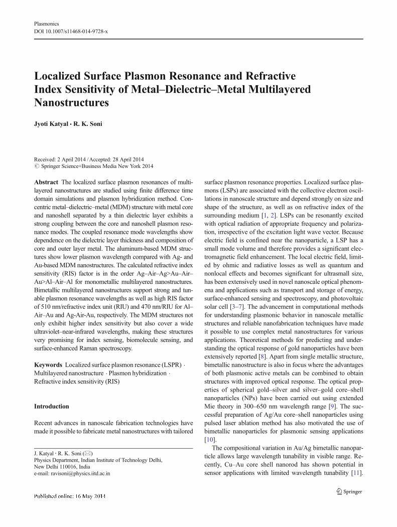
An isolated concentric metal–dielectric–metal (MDM) multi-layered nanostructure is irradiated with an optical field in thexy-plane, propagating along the y-direction and polarizedalong the x-direction, as illustrated in Fig. 1 by symbols kand E, respectively. The two concentric metallic layers havingradius as R1 and R3 are separated by a thin dielectric layer ofthickness t=R2−R1. The inner solid sphere and outer shell arecomposed of different metals with dielectric permittivity εM1
and εM2, respectively, and ε1 and ε2 are the permittivity ofdielectric layer and surrounding medium. Here, we employedLumerical’s FDTD solutions to carry out simulations of LSPRproperties of multilayered nanostructures [17]. We adopted a
cubic Yee cell of 1 nm side and a time stepΔt=1.31×10⁻¹⁸s,bounded by Courant condition. The grid sizes in the x, y, and zdirections were chosen in such a way that the values of E-fieldintensities around the nanoparticle become independent of thegrid size. This process was carried out by initially selectinggrid sizes in the x, y, and z directions of the order of 1/10th ofthe size of the nanosphere and subsequently reducing thevalue of the grid spacing until further reduction in the gridspacing had no influence on the calculated results around thenanosphere. The FDTD software employed in this work al-lows selection of different grid sizes for the edges of metallicnanostructure and the bulk media. In our calculation, 0.7 nmgrid spacing is chosen for spacing around the nanosphere. Thematerial data is chosen from Johnson and Christy and Palik forAu and Ag, respectively, whereas the material data of Al istaken from Palik for wavelengths >200 nm and CRCmodel ischosen for wavelengths <200 nm [17].
Results and Discussion
The absorption spectra for MDM structure of different compo-sitions are calculated. Initially, the dielectric effect is neglectedby setting ε1=ε2=1, and the core as well as the outer shell isassumed to be made of the same metal (εM1=εM2). A simpleresult is obtained on this assumption from which the stabilityand tunability can be seen directly. The characteristics of thesurface plasmon resonance spectra for MDM structures primar-ily depend on the properties of the SPR of two constituent metalcore and outer shell layer and their coupling strength, deter-mined by the thickness of the dielectric spacer layer. Thedependence of optical response on geometrical parametershas already been reported [18]; therefore, here, we focus onthe structural composition. For this, we have chosen a config-uration where total size of the particle is constant but the metalcore radius and composition is varied.
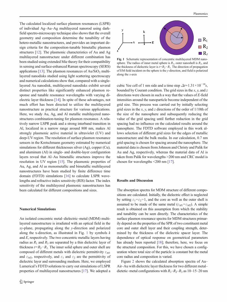
Figure 2 shows the calculated absorption spectra of Au–Air–Auwith dielectric layer thickness for two different metal–dietetic–metal configurations with R1–R2–R3 as 10–15–20 nm
Fig. 1 Schematic representation of concentric multilayered MDM nano-sphere. The radius of inner metal sphere is R1, outer nanoshell is R3, andthe thickness of dielectric layer is t=R2−R1. The direction of propagationof EM field incident on the sphere is the y-direction, and field is polarizedalong the x-axis
Plasmonics
and 15–20–25 nm. The absorption spectra of both the struc-tures show two LSPR peaks which broaden and red shift withincrease in particle size. The calculated peaks are at 510 and593 nm for smaller (10–15–20 nm) structures and 511 and690 nm for larger (15–20–25 nm) structures. The shorterwavelength peak is attributed to bare Au nanosphere whereasthe longer wavelength peak occurs due to contribution of theouter Au nanoshell. Our calculated absorption spectra ofMDM structure in vacuum are in qualitative agreement withthe classical Mie calculations of two LSPR absorption peaksin the spectra of MDM nanostructures of different composi-tions for a fixed 5 nm dielectric layer in water [13]. The stronglonger wavelength resonance peak provides an additionaltunability in the MDM structure compared with bare nano-sphere of same size.
Since the strength of the coupling between the metal coreand metal nanoshell in MDM structure depends on the thick-ness of dielectric spacer layer, the effect of thickness ofdielectric layer is therefore studied. The calculated absorptionspectra for different thickness of dielectric layer are shown inFig. 2, where the core size is varied from 10 to 14 nm and 15 to20 nm in a step of 1 nm in 10–15–20 nm and 15–20–25 nm,respectively, in MDM structure. The longer wavelength peak
gradually red shifts, and its intensity decreases with decreasein thickness of the dielectric layer. Furthermore, the absorptionspectra of MDM structure with extremely thin dielectric layerexhibit a single dipolar resonance peak. The intensities of twocalculated plasmon resonance peaks of 17–20–25 nm MDMstructure at 511 and 812 nm are nearly equal. Clearly,MDM structure provides a unique advantage of strongand nearly equal plasmonic response simultaneously invisible and near-infrared (NIR) wavelengths which isnot possible with metal nanosphere or oxide-coatedmetal nanosphere. In Au–SiO2–Au, multilayered nano-shell shows a red shift of SPR peaks with decreasingintensity and increasing radius of Au core due to de-crease in the intermediate silica layer thickness andleads to a stronger plasmonic coupling [18]. The extratunability introduced by the silica layer provides anopportunity for controlling the strength and resonanceenergy of the plasmon modes of the metallic nanoparticles.Apart from inner core, the effect of outer shell is also equallyimportant. Mie calculations have shown that, with increasingthickness of the outer shell, the low-energy resonance blueshifts but the high-energy resonance red shifts, and when theshell becomes thick, the broadened dipolar resonances appearvery close and separated by a sharp dip which can be exploitedin many applications [18].
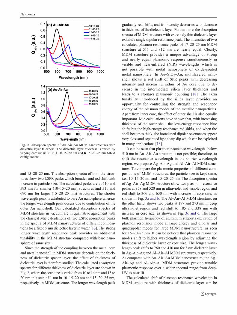
It can be seen that plasmon resonance wavelengths below510 nm in Au–Air–Au structure is not possible; therefore, toshift the resonance wavelength in the shorter wavelengthregion, we propose Ag–Air–Ag and Al–Air–Al MDM struc-tures. To compare the plasmonic properties of different com-positions of MDM structures, the particle size is kept same,i.e., 10–15–20 nm and 15–20–25 nm. The absorption spectraof Ag–Air–Ag MDM structure show two plasmon resonancepeaks at 358 and 520 nm in ultraviolet and visible region andred shift to 366 and 630 nm with increase in core size, asshown in Fig. 3a and b. The Al–Air–Al MDM structure, onthe other hand, shows two peaks at 177 and 273 nm in deepultraviolet region and red shift to 185 and 338 nm withincrease in core size, as shown in Fig. 3c and d. The largebulk plasmon frequency of aluminum supports excitation ofplasmon resonance mode at large energy and dipolar andquadrupolar modes for large MDM nanostructure, as seenfor 15–20–25 nm. It can be noticed that plasmon resonancemodes shift to higher wavelength region by adjusting thethickness of dielectric layer or core size. The longer wave-length peak shifts to 760 and 430 nm for 3 nm dielectric layerin Ag–Air–Ag and Al–Air–Al MDM structures, respectively.As compared with Au–Air–Au MDM nanostructure, the Ag–Air–Ag and Al–Air–Al MDM structures provide tunableplasmonic response over a wider spectral range from deep-UV to near IR.
The calculated shift of plasmon resonance wavelength inMDM structure with thickness of dielectric layer can be
500 600 700 800 900 10000.0
0.1
0.2
0.3
0.4
0.5
0.6
0.7
Qab
s(a
.u.)
Qab
s(a
.u.)
Wavelength (nm)
10-15-20 11-15-20 12-15-20 13-15-20 14-15-20
(a) Au-Air-Au
500 600 700 800 900 10000.0
0.2
0.4
0.6
0.8
1.0
1.2
1.4(b) Au-Air-Au
Wavelength (nm)
15-20-25 16-20-25 17-20-25 18-20-25 19-20-25
Fig. 2 Absorption spectra of Au–Air–Au MDM nanostructures withdielectric layer thickness. The dielectric layer thickness is varied byvarying core radius R1 in a 10–15–20 nm and b 15–20–25 nm MDMconfigurations
Plasmonics
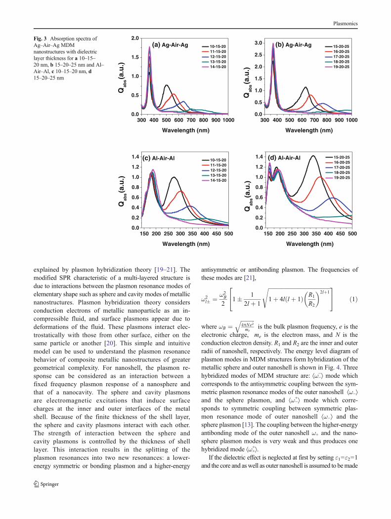
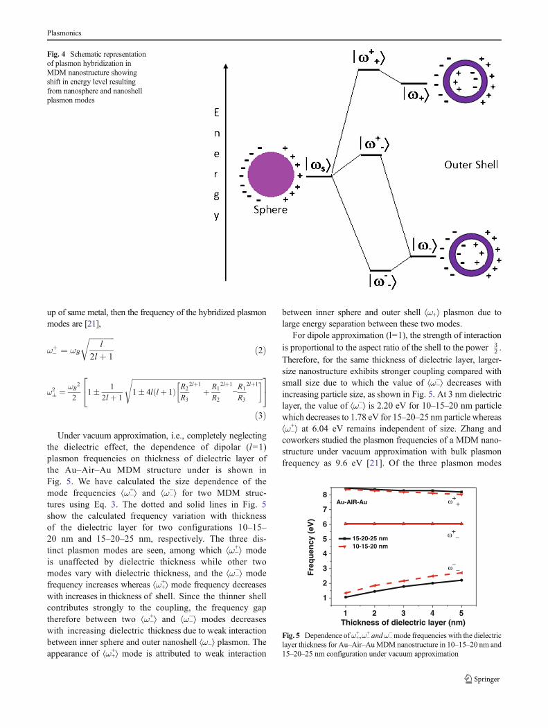
explained by plasmon hybridization theory [19–21]. Themodified SPR characteristic of a multi-layered structure isdue to interactions between the plasmon resonance modes ofelementary shape such as sphere and cavity modes of metallicnanostructures. Plasmon hybridization theory considersconduction electrons of metallic nanoparticle as an in-compressible fluid, and surface plasmons appear due todeformations of the fluid. These plasmons interact elec-trostatically with those from other surface, either on thesame particle or another [20]. This simple and intuitivemodel can be used to understand the plasmon resonancebehavior of composite metallic nanostructures of greatergeometrical complexity. For nanoshell, the plasmon re-sponse can be considered as an interaction between afixed frequency plasmon response of a nanosphere andthat of a nanocavity. The sphere and cavity plasmonsare electromagnetic excitations that induce surfacecharges at the inner and outer interfaces of the metalshell. Because of the finite thickness of the shell layer,the sphere and cavity plasmons interact with each other.The strength of interaction between the sphere andcavity plasmons is controlled by the thickness of shelllayer. This interaction results in the splitting of theplasmon resonances into two new resonances: a lower-energy symmetric or bonding plasmon and a higher-energy
antisymmetric or antibonding plasmon. The frequencies ofthese modes are [21],
ω2l� ¼ ω2
B
21� 1
2l þ 1
ffiffiffiffiffiffiffiffiffiffiffiffiffiffiffiffiffiffiffiffiffiffiffiffiffiffiffiffiffiffiffiffiffiffiffiffiffiffiffiffiffiffiffiffiffi1þ 4l l þ 1ð Þ R1
R2
� �2lþ1s2
435 ð1Þ
where ωB ¼ffiffiffiffiffiffiffiffiffiffi4πNe2me
qis the bulk plasmon frequency, e is the
electronic charge, me is the electron mass, and N is theconduction electron density. R1 and R2 are the inner and outerradii of nanoshell, respectively. The energy level diagram ofplasmon modes in MDM structures form hybridization of themetallic sphere and outer nanoshell is shown in Fig. 4. Threehybridized modes of MDM structure are: ⟨ω−
−⟩ mode whichcorresponds to the antisymmetric coupling between the sym-metric plasmon resonance modes of the outer nanoshell ⟨ω−⟩and the sphere plasmon, and ⟨ω−
+⟩ mode which corre-sponds to symmetric coupling between symmetric plas-mon resonance mode of outer nanoshell ⟨ω−⟩ and thesphere plasmon [13]. The coupling between the higher-energyantibonding mode of the outer nanoshell ω+ and the nano-sphere plasmon modes is very weak and thus produces onehybridized mode ⟨ω+
+⟩.If the dielectric effect is neglected at first by setting ε1=ε2=1
and the core and aswell as outer nanoshell is assumed to bemade
300 400 500 600 700 800 900 10000.0
0.5
1.0
1.5
2.0
Qab
s(a
.u.)
Wavelength (nm)
10-15-20 11-15-20 12-15-20 13-15-20 14-15-20
(a) Ag-Air-Ag
300 400 500 600 700 800 900 10000.0
0.5
1.0
1.5
2.0
2.5
3.0
Qab
s(a
.u.)
Wavelength (nm)
15-20-25 16-20-25 17-20-25 18-20-25 19-20-25
(b) Ag-Air-Ag
150 200 250 300 350 400 450 5000.0
0.2
0.4
0.6
0.8
1.0
1.2
1.4
Qab
s(a
.u.)
Wavelength (nm)
10-15-20 11-15-20 12-15-20 13-15-20 14-15-20
(c) Al-Air-Al
150 200 250 300 350 400 450 5000.0
0.2
0.4
0.6
0.8
1.0
1.2
1.4
Qab
s(a
.u.)
Wavelength (nm)
15-20-25 16-20-25 17-20-25 18-20-25 19-20-25
(d) Al-Air-Al
Fig. 3 Absorption spectra ofAg–Air–Ag MDMnanostructures with dielectriclayer thickness for a 10–15–20 nm, b 15–20–25 nm and Al–Air–Al, c 10–15–20 nm, d15–20–25 nm
Plasmonics
up of same metal, then the frequency of the hybridized plasmonmodes are [21],
ωþ− ¼ ωB
ffiffiffiffiffiffiffiffiffiffiffiffiffil
2l þ 1
rð2Þ
ω2� ¼ ωB
2
21� 1
2l þ 1
ffiffiffiffiffiffiffiffiffiffiffiffiffiffiffiffiffiffiffiffiffiffiffiffiffiffiffiffiffiffiffiffiffiffiffiffiffiffiffiffiffiffiffiffiffiffiffiffiffiffiffiffiffiffiffiffiffiffiffiffiffiffiffiffiffiffiffiffiffiffiffiffiffiffiffiffiffi1� 4l l þ 1ð Þ R2
R3
2lþ1
þ R1
R2
2lþ1
−R1
R3
2lþ1� �s24
35
ð3Þ
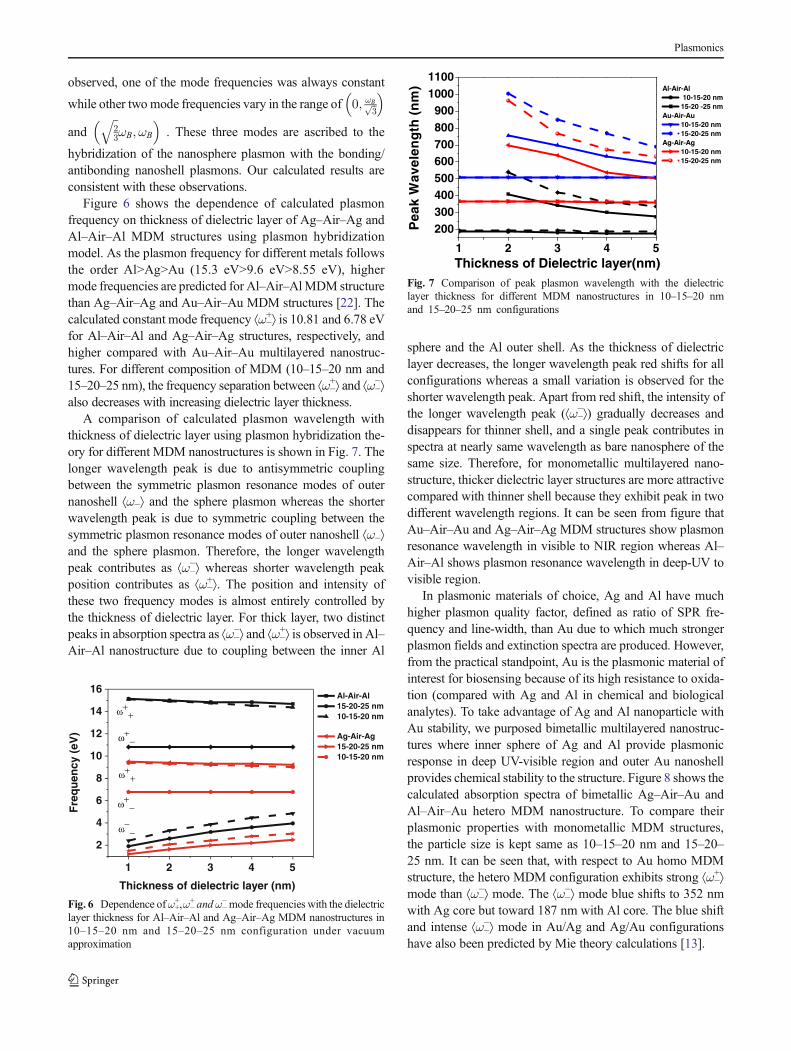
Under vacuum approximation, i.e., completely neglectingthe dielectric effect, the dependence of dipolar (l=1)plasmon frequencies on thickness of dielectric layer ofthe Au–Air–Au MDM structure under is shown inFig. 5. We have calculated the size dependence of themode frequencies ⟨ω−
+⟩ and ⟨ω−−⟩ for two MDM struc-
tures using Eq. 3. The dotted and solid lines in Fig. 5show the calculated frequency variation with thicknessof the dielectric layer for two configurations 10–15–20 nm and 15–20–25 nm, respectively. The three dis-tinct plasmon modes are seen, among which ⟨ω−
+⟩ modeis unaffected by dielectric thickness while other twomodes vary with dielectric thickness, and the ⟨ω−
−⟩ modefrequency increases whereas ⟨ω+
+⟩ mode frequency decreaseswith increases in thickness of shell. Since the thinner shellcontributes strongly to the coupling, the frequency gaptherefore between two ⟨ω−
+⟩ and ⟨ω−−⟩ modes decreases
with increasing dielectric thickness due to weak interactionbetween inner sphere and outer nanoshell ⟨ω−⟩ plasmon. Theappearance of ⟨ω+
+⟩ mode is attributed to weak interaction
between inner sphere and outer shell ⟨ω+⟩ plasmon due tolarge energy separation between these two modes.
For dipole approximation (l=1), the strength of interactionis proportional to the aspect ratio of the shell to the power 3
2 .Therefore, for the same thickness of dielectric layer, larger-size nanostructure exhibits stronger coupling compared withsmall size due to which the value of ⟨ω−
−⟩ decreases withincreasing particle size, as shown in Fig. 5. At 3 nm dielectriclayer, the value of ⟨ω−
−⟩ is 2.20 eV for 10–15–20 nm particlewhich decreases to 1.78 eV for 15–20–25 nm particle whereas⟨ω−
+⟩ at 6.04 eV remains independent of size. Zhang andcoworkers studied the plasmon frequencies of a MDM nano-structure under vacuum approximation with bulk plasmonfrequency as 9.6 eV [21]. Of the three plasmon modes
Fig. 4 Schematic representationof plasmon hybridization inMDM nanostructure showingshift in energy level resultingfrom nanosphere and nanoshellplasmon modes
1 2 3 4 5
1
2
3
4
5
6
7
8
15-20-25 nm 10-15-20 nm
Fre
qu
ency
(eV
)
Au-AIR-Au
Thickness of dielectric layer (nm)
Fig. 5 Dependence ofω++,ω−
+ andω−−mode frequencies with the dielectric
layer thickness for Au–Air–AuMDM nanostructure in 10–15–20 nm and15–20–25 nm configuration under vacuum approximation
Plasmonics
observed, one of the mode frequencies was always constant
while other two mode frequencies vary in the range of 0; ωBffiffi3
p� �
andffiffi23
qωB;ωB
� �. These three modes are ascribed to the
hybridization of the nanosphere plasmon with the bonding/antibonding nanoshell plasmons. Our calculated results areconsistent with these observations.
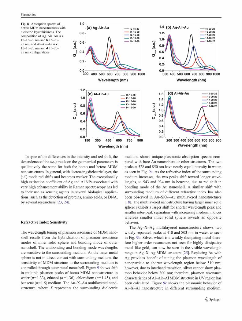
Figure 6 shows the dependence of calculated plasmonfrequency on thickness of dielectric layer of Ag–Air–Ag andAl–Air–Al MDM structures using plasmon hybridizationmodel. As the plasmon frequency for different metals followsthe order Al>Ag>Au (15.3 eV>9.6 eV>8.55 eV), highermode frequencies are predicted for Al–Air–AlMDM structurethan Ag–Air–Ag and Au–Air–Au MDM structures [22]. Thecalculated constant mode frequency ⟨ω−
+⟩ is 10.81 and 6.78 eVfor Al–Air–Al and Ag–Air–Ag structures, respectively, andhigher compared with Au–Air–Au multilayered nanostruc-tures. For different composition of MDM (10–15–20 nm and15–20–25 nm), the frequency separation between ⟨ω−
+⟩ and ⟨ω−−⟩
also decreases with increasing dielectric layer thickness.A comparison of calculated plasmon wavelength with
thickness of dielectric layer using plasmon hybridization the-ory for different MDM nanostructures is shown in Fig. 7. Thelonger wavelength peak is due to antisymmetric couplingbetween the symmetric plasmon resonance modes of outernanoshell ⟨ω−⟩ and the sphere plasmon whereas the shorterwavelength peak is due to symmetric coupling between thesymmetric plasmon resonance modes of outer nanoshell ⟨ω−⟩and the sphere plasmon. Therefore, the longer wavelengthpeak contributes as ⟨ω−
−⟩ whereas shorter wavelength peakposition contributes as ⟨ω−
+⟩. The position and intensity ofthese two frequency modes is almost entirely controlled bythe thickness of dielectric layer. For thick layer, two distinctpeaks in absorption spectra as ⟨ω−
−⟩ and ⟨ω−+⟩ is observed in Al–
Air–Al nanostructure due to coupling between the inner Al
sphere and the Al outer shell. As the thickness of dielectriclayer decreases, the longer wavelength peak red shifts for allconfigurations whereas a small variation is observed for theshorter wavelength peak. Apart from red shift, the intensity ofthe longer wavelength peak (⟨ω−
−⟩) gradually decreases anddisappears for thinner shell, and a single peak contributes inspectra at nearly same wavelength as bare nanosphere of thesame size. Therefore, for monometallic multilayered nano-structure, thicker dielectric layer structures are more attractivecompared with thinner shell because they exhibit peak in twodifferent wavelength regions. It can be seen from figure thatAu–Air–Au and Ag–Air–Ag MDM structures show plasmonresonance wavelength in visible to NIR region whereas Al–Air–Al shows plasmon resonance wavelength in deep-UV tovisible region.
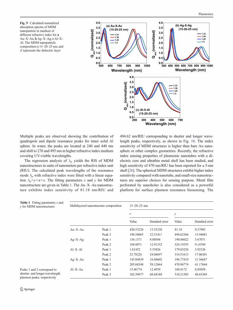
In plasmonic materials of choice, Ag and Al have muchhigher plasmon quality factor, defined as ratio of SPR fre-quency and line-width, than Au due to which much strongerplasmon fields and extinction spectra are produced. However,from the practical standpoint, Au is the plasmonic material ofinterest for biosensing because of its high resistance to oxida-tion (compared with Ag and Al in chemical and biologicalanalytes). To take advantage of Ag and Al nanoparticle withAu stability, we purposed bimetallic multilayered nanostruc-tures where inner sphere of Ag and Al provide plasmonicresponse in deep UV-visible region and outer Au nanoshellprovides chemical stability to the structure. Figure 8 shows thecalculated absorption spectra of bimetallic Ag–Air–Au andAl–Air–Au hetero MDM nanostructure. To compare theirplasmonic properties with monometallic MDM structures,the particle size is kept same as 10–15–20 nm and 15–20–25 nm. It can be seen that, with respect to Au homo MDMstructure, the hetero MDM configuration exhibits strong ⟨ω−
+⟩mode than ⟨ω−
−⟩ mode. The ⟨ω−−⟩ mode blue shifts to 352 nm
with Ag core but toward 187 nm with Al core. The blue shiftand intense ⟨ω−
−⟩ mode in Au/Ag and Ag/Au configurationshave also been predicted by Mie theory calculations [13].
1 2 3 4 5
2
4
6
8
10
12
14
16 Al-Air-Al 15-20-25 nm 10-15-20 nm
Ag-Air-Ag 15-20-25 nm 10-15-20 nm
Fre
qu
ency
(eV
)
Thickness of dielectric layer (nm)
Fig. 6 Dependence ofω++,ω−
+ andω−−mode frequencies with the dielectric
layer thickness for Al–Air–Al and Ag–Air–Ag MDM nanostructures in10–15–20 nm and 15–20–25 nm configuration under vacuumapproximation
1 2 3 4 5
200300400500600700800900
10001100
Pea
k W
avel
eng
th (
nm
)
Thickness of Dielectric layer(nm)
Al-Air-Al 10-15-20 nm 15-20 -25 nm
Au-Air-Au 10-15-20 nm 15-20-25 nm
Ag-Air-Ag 10-15-20 nm 15-20-25 nm
Fig. 7 Comparison of peak plasmon wavelength with the dielectriclayer thickness for different MDM nanostructures in 10–15–20 nmand 15–20–25 nm configurations
Plasmonics
In spite of the differences in the intensity and red shift, thedependence of the ⟨ω−
−⟩mode on the geometrical parameters isqualitatively the same for both the homo and hetero MDMnanostructures. In general, with decreasing dielectric layer, the⟨ω−
−⟩ mode red shifts and becomes weaker. The exceptionallyhigh extinction coefficient of Ag and Al NPs associated withvery high enhancement ability in Raman spectroscopy has ledto their use as sensing agents in several biological applica-tions, such as the detection of proteins, amino acids, or DNA,by several researchers [23, 24].
Refractive Index Sensitivity
The wavelength tuning of plasmon resonance of MDM nano-shell results from the hybridization of plasmon resonancemodes of inner solid sphere and bonding mode of outernanoshell. The antibonding and bonding mode wavelengthsare sensitive to the surrounding medium. As the inner metalsphere is not in direct contact with surrounding medium, thesensitivity of MDM structure to the surrounding medium iscontrolled through outer metal nanoshell. Figure 9 shows shiftin multiple plasmon peaks of homo MDM nanostructure inwater (n=1.33), ethanol (n=1.36), chloroform (n=1.45), andbenzene (n=1.5) medium. The Au–X–Au multilayered nano-structure, where X represents the surrounding dielectric
medium, shows unique plasmonic absorption spectra com-pared with bare Au nanosphere or other structures. The twopeaks at 528 and 850 nm have nearly equal intensity in water,as seen in Fig. 9a. As the refractive index of the surroundingmedium increases, the two peaks shift toward longer wave-lengths, to 543 and 934 nm in benzene, due to red shift inbonding mode of the Au nanoshell. A similar shift withsurrounding medium of different refractive index has alsobeen observed in Au–SiO2–Au multilayered nanostructures[18]. The multilayered nanostructure having larger inner solidsphere exhibits a larger shift for shorter wavelength peak andsmaller inter-peak separation with increasing medium indiceswhereas smaller inner solid sphere reveals an oppositebehavior.
The Ag–X–Ag multilayered nanostructure shows twowidely separated peaks at 410 and 803 nm in water, as seenin Fig. 9b. Silver, which is a weakly dissipating metal there-fore higher-order resonances not seen for highly dissipativemetal like gold, can now be seen in the visible wavelengthrange in Ag–X–Ag MDM structure [25]. Replacing Au withAg provides benefit of tuning the plasmon wavelength ofnanoparticle to shorter wavelength region below 510 nm;however, due to interband transition, silver cannot show plas-mon behavior below 300 nm; therefore, plasmon resonancecharacteristics of Al–Air–AlMDM structure in UVregion hasbeen calculated. Figure 9c shows the plasmonic behavior ofAl–X–Al nanostructure in different surrounding medium.
300 400 500 600 700 800 900 10000.0
0.2
0.4
0.6
0.8
1.0
Wavelength (nm)
10-15-20 11-15-20 12-15-20 13-15-20 14-15-20
(a) Ag-Air-Au
300 400 500 600 700 800 900 10000.0
0.2
0.4
0.6
0.8
1.0
1.2
1.4
Qab
s(a
.u.)
Qab
s(a
.u.)
Qab
s(a
.u.)
Qab
s(a
.u.)
Wavelength (nm)
15-20-25 16-20-25 17-20-25 18-20-25 19-20-25
(b) Ag-Air-Au
150 300 450 600 750 9000.0
0.2
0.4
0.6
0.8
1.0
1.2
Wavelength (nm)
10-15-20 11-15-20 12-15-20 13-15-20 14-15-20
(c) Al-Air-Au
200 300 400 500 600 700 800 9000.0
0.2
0.4
0.6
0.8
1.0
1.2
1.4
1.6
Wavelength (nm)
(d) Al-Air-Au 15-20-25 16-20-25 17-20-25 18-20-25 19-20-25
Fig. 8 Absorption spectra ofhetero MDM nanostructures withdielectric layer thickness. Thecomposition of Ag–Air–Au is a10–15–20 nm and b 15–20–25 nm, and Al–Air–Au is c10–15–20 nm and d 15–20–25 nm configurations
Plasmonics
Multiple peaks are observed showing the contribution ofquadrupole and dipole resonance peaks for inner solid Alsphere. In water, the peaks are located at 240 and 440 nmand shift to 270 and 495 nm in higher refractive index mediumcovering UV-visible wavelengths.
The regression analysis of λp yields the RIS of MDMnanostructures in units of nanometers per refractive index unit(RIU). The calculated peak wavelengths of the resonancemode λp with refractive index were fitted with a linear equa-tion λp=y×n+x. The fitting parameters x and y for MDMnanostructure are given in Table 1. The Au–X–Au nanostruc-ture exhibits index sensitivity of 81.18 nm/RIU and
494.62 nm/RIU corresponding to shorter and longer wave-length peaks, respectively, as shown in Fig. 10. The indexsensitivity of MDM structures is higher than bare Au nano-sphere or other complex geometries. Recently, the refractiveindex sensing properties of plasmonic nanotubes with a di-electric core and ultrathin metal shell has been studied, andhigh sensitivity of 470 nm/RIU has been reported for a 5-nmshell [26]. The spherical MDM structures exhibit higher indexsensitivity compared with nanotube, and small-size nanostruc-tures are superior choices for sensing purpose. Metal filmperforated by nanoholes is also considered as a powerfulplatform for surface plasmon resonance biosensing. The
500 600 700 800 900 10000.00.51.01.52.02.53.03.54.0
1.33 1.36 1.45 1.5
Qab
s(nor
mal
ized
)
(a) Au-X-Au (15-20-25 nm)
Wavelength (nm)300 400 500 600 700 800 900 1000
0.00.51.01.52.02.53.03.54.0
1.33 1.36 1.45 1.5
Qab
s(nor
mal
ized
)
(b) Ag-X-Ag (15-20-25 nm)
Wavelength (nm)
200 300 400 500 600 7000.00.51.01.52.02.53.03.54.0
Qab
s(nor
mal
ized
)
(c) Al-X-Al (15-20-25 nm)
1.33 1.36 1.45 1.5
Wavelength (nm)
Fig. 9 Calculated normalizedabsorption spectra of MDMnanoparticle in medium ofdifferent refractive index for aAu–X–Au, bAg–X–Ag, cAl–X–Al. The MDM nanoparticlecomposition is 15–20–25 nm, andX represents the dielectric layer
Table 1 Fitting parameters x andy for MDM nanostructures
Peaks 1 and 2 correspond toshorter- and longer-wavelengthplasmon peaks, respectively
Multilayered nanostructure composition 15–20–25 nm
x y
Value Standard error Value Standard error
Au–X–Au Peak 1 420.53226 13.52338 81.18 9.57985
Peak 2 190.58065 22.51411 494.62366 15.94881
Ag–X–Ag Peak 1 156.1371 8.00504 190.86022 5.67071
Peak 2 104.8871 12.91332 524.19355 9.14769
Al–X–Al Peak 1 1.81452 5.53826 179.03226 3.92326
Peak 2 23.78226 24.08697 314.51613 17.06301
Ag–X–Au Peak 1 145.04839 16.04602 196.77419 11.36687
Peak 2 205.68548 58.12664 470.96774 41.17644
Al–X–Au Peak 1 15.46774 12.4939 168.8172 8.85058
Peak 2 102.59677 68.68188 510.21505 48.65369
Plasmonics
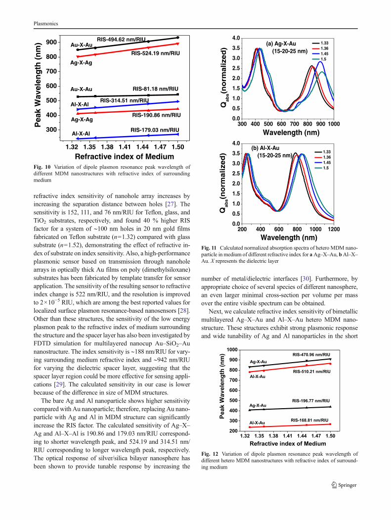
refractive index sensitivity of nanohole array increases byincreasing the separation distance between holes [27]. Thesensitivity is 152, 111, and 76 nm/RIU for Teflon, glass, andTiO2 substrates, respectively, and found 40 % higher RISfactor for a system of ∼100 nm holes in 20 nm gold filmsfabricated on Teflon substrate (n=1.32) compared with glasssubstrate (n=1.52), demonstrating the effect of refractive in-dex of substrate on index sensitivity. Also, a high-performanceplasmonic sensor based on transmission through nanoholearrays in optically thick Au films on poly (dimethylsiloxane)substrates has been fabricated by template transfer for sensorapplication. The sensitivity of the resulting sensor to refractiveindex change is 522 nm/RIU, and the resolution is improvedto 2×10⁻⁵ RIU, which are among the best reported values forlocalized surface plasmon resonance-based nanosensors [28].Other than these structures, the sensitivity of the low energyplasmon peak to the refractive index of medium surroundingthe structure and the spacer layer has also been investigated byFDTD simulation for multilayered nanocup Au–SiO2–Aunanostructure. The index sensitivity is ∼188 nm/RIU for vary-ing surrounding medium refractive index and ∼942 nm/RIUfor varying the dielectric spacer layer, suggesting that thespacer layer region could be more effective for sensing appli-cations [29]. The calculated sensitivity in our case is lowerbecause of the difference in size of MDM structures.
The bare Ag and Al nanoparticle shows higher sensitivitycompared with Au nanoparticle; therefore, replacing Au nano-particle with Ag and Al in MDM structure can significantlyincrease the RIS factor. The calculated sensitivity of Ag–X–Ag and Al–X–Al is 190.86 and 179.03 nm/RIU correspond-ing to shorter wavelength peak, and 524.19 and 314.51 nm/RIU corresponding to longer wavelength peak, respectively.The optical response of silver/silica bilayer nanosphere hasbeen shown to provide tunable response by increasing the
number of metal/dielectric interfaces [30]. Furthermore, byappropriate choice of several species of different nanosphere,an even larger minimal cross-section per volume per massover the entire visible spectrum can be obtained.
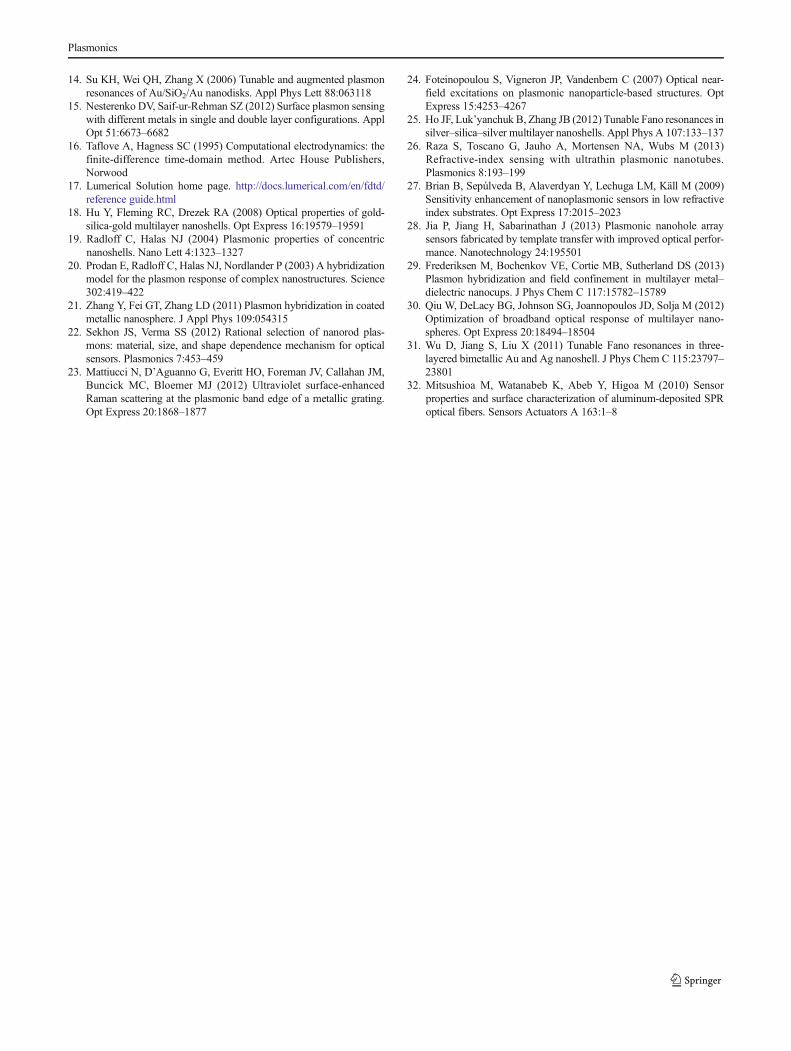
Next, we calculate refractive index sensitivity of bimetallicmultilayered Ag–X–Au and Al–X–Au hetero MDM nano-structure. These structures exhibit strong plasmonic responseand wide tunability of Ag and Al nanoparticles in the short
1.32 1.35 1.38 1.41 1.44 1.47 1.50
300
400
500
600
700
800
900
RIS-524.19 nm/RIU
Ag-X-Ag
RIS-314.51 nm/RIUAl-X-Al
Pea
k W
avel
eng
th (
nm
)
Refractive index of Medium
Ag-X-Ag
Al-X-Al
Au-X-Au
Au-X-AuRIS-494.62 nm/RIU
RIS-81.18 nm/RIU
RIS-190.86 nm/RIU
RIS-179.03 nm/RIU
Fig. 10 Variation of dipole plasmon resonance peak wavelength ofdifferent MDM nanostructures with refractive index of surroundingmedium
300 400 500 600 700 800 900 10000.0
0.5
1.0
1.5
2.0
2.5
3.0
3.5
4.0
Qab
s(n
orm
ali
zed
)
(a) Ag-X-Au (15-20-25 nm)
1.33 1.36 1.45 1.5
Wavelength (nm)
200 400 600 800 1000 12000.0
0.5
1.0
1.5
2.0
2.5
3.0
3.5
4.0
Qab
s(n
orm
ali
zed
)
(b) Al-X-Au (15-20-25 nm)
1.33 1.36 1.45 1.5
Wavelength (nm)Fig. 11 Calculated normalized absorption spectra of hetero MDM nano-particle in medium of different refractive index for aAg–X–Au, bAl–X–Au. X represents the dielectric layer
1.32 1.35 1.38 1.41 1.44 1.47 1.50200
300
400
500
600
700
800
900
1000
Ag-X-Au
Peak
Wav
elen
gth
(nm
)
Ag-X-Au
RIS-168.81 nm/RIU
RIS-196.77 nm/RIU
RIS-470.96 nm/RIU
Al-X-Au
Refractive index of Medium
Al-X-AuRIS-510.21 nm/RIU
Fig. 12 Variation of dipole plasmon resonance peak wavelength ofdifferent hetero MDM nanostructures with refractive index of surround-ing medium
Plasmonics
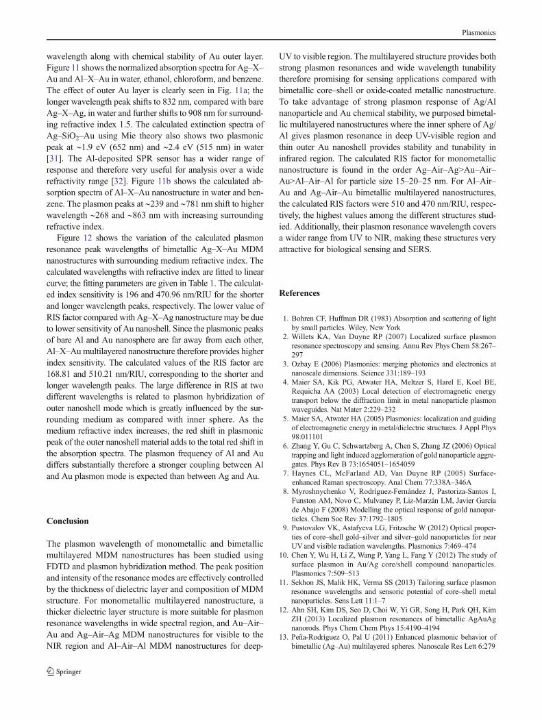
wavelength along with chemical stability of Au outer layer.Figure 11 shows the normalized absorption spectra for Ag–X–Au and Al–X–Au in water, ethanol, chloroform, and benzene.The effect of outer Au layer is clearly seen in Fig. 11a; thelonger wavelength peak shifts to 832 nm, compared with bareAg–X–Ag, in water and further shifts to 908 nm for surround-ing refractive index 1.5. The calculated extinction spectra ofAg–SiO2–Au using Mie theory also shows two plasmonicpeak at ∼1.9 eV (652 nm) and ∼2.4 eV (515 nm) in water[31]. The Al-deposited SPR sensor has a wider range ofresponse and therefore very useful for analysis over a widerefractivity range [32]. Figure 11b shows the calculated ab-sorption spectra of Al–X–Au nanostructure in water and ben-zene. The plasmon peaks at ∼239 and ∼781 nm shift to higherwavelength ∼268 and ∼863 nm with increasing surroundingrefractive index.
Figure 12 shows the variation of the calculated plasmonresonance peak wavelengths of bimetallic Ag–X–Au MDMnanostructures with surrounding medium refractive index. Thecalculated wavelengths with refractive index are fitted to linearcurve; the fitting parameters are given in Table 1. The calculat-ed index sensitivity is 196 and 470.96 nm/RIU for the shorterand longer wavelength peaks, respectively. The lower value ofRIS factor compared with Ag–X–Ag nanostructure may be dueto lower sensitivity of Au nanoshell. Since the plasmonic peaksof bare Al and Au nanosphere are far away from each other,Al–X–Aumultilayered nanostructure therefore provides higherindex sensitivity. The calculated values of the RIS factor are168.81 and 510.21 nm/RIU, corresponding to the shorter andlonger wavelength peaks. The large difference in RIS at twodifferent wavelengths is related to plasmon hybridization ofouter nanoshell mode which is greatly influenced by the sur-rounding medium as compared with inner sphere. As themedium refractive index increases, the red shift in plasmonicpeak of the outer nanoshell material adds to the total red shift inthe absorption spectra. The plasmon frequency of Al and Audiffers substantially therefore a stronger coupling between Aland Au plasmon mode is expected than between Ag and Au.
Conclusion
The plasmon wavelength of monometallic and bimetallicmultilayered MDM nanostructures has been studied usingFDTD and plasmon hybridization method. The peak positionand intensity of the resonance modes are effectively controlledby the thickness of dielectric layer and composition of MDMstructure. For monometallic multilayered nanostructure, athicker dielectric layer structure is more suitable for plasmonresonance wavelengths in wide spectral region, and Au–Air–Au and Ag–Air–Ag MDM nanostructures for visible to theNIR region and Al–Air–Al MDM nanostructures for deep-
UV to visible region. The multilayered structure provides bothstrong plasmon resonances and wide wavelength tunabilitytherefore promising for sensing applications compared withbimetallic core–shell or oxide-coated metallic nanostructure.To take advantage of strong plasmon response of Ag/Alnanoparticle and Au chemical stability, we purposed bimetal-lic multilayered nanostructures where the inner sphere of Ag/Al gives plasmon resonance in deep UV-visible region andthin outer Au nanoshell provides stability and tunability ininfrared region. The calculated RIS factor for monometallicnanostructure is found in the order Ag–Air–Ag>Au–Air–Au>Al–Air–Al for particle size 15–20–25 nm. For Al–Air–Au and Ag–Air–Au bimetallic multilayered nanostructures,the calculated RIS factors were 510 and 470 nm/RIU, respec-tively, the highest values among the different structures stud-ied. Additionally, their plasmon resonance wavelength coversa wider range from UV to NIR, making these structures veryattractive for biological sensing and SERS.
References
1. Bohren CF, Huffman DR (1983) Absorption and scattering of lightby small particles. Wiley, New York
2. Willets KA, Van Duyne RP (2007) Localized surface plasmonresonance spectroscopy and sensing. Annu Rev Phys Chem 58:267–297
3. Ozbay E (2006) Plasmonics: merging photonics and electronics atnanoscale dimensions. Science 331:189–193
4. Maier SA, Kik PG, Atwater HA, Meltzer S, Harel E, Koel BE,Requicha AA (2003) Local detection of electromagnetic energytransport below the diffraction limit in metal nanoparticle plasmonwaveguides. Nat Mater 2:229–232
5. Maier SA, Atwater HA (2005) Plasmonics: localization and guidingof electromagnetic energy in metal/dielectric structures. J Appl Phys98:011101
6. Zhang Y, Gu C, Schwartzberg A, Chen S, Zhang JZ (2006) Opticaltrapping and light induced agglomeration of gold nanoparticle aggre-gates. Phys Rev B 73:1654051–1654059
7. Haynes CL, McFarland AD, Van Duyne RP (2005) Surface-enhanced Raman spectroscopy. Anal Chem 77:338A–346A
8. Myroshnychenko V, Rodríguez-Fernández J, Pastoriza-Santos I,Funston AM, Novo C, Mulvaney P, Liz-Marzán LM, Javier Garcíade Abajo F (2008) Modelling the optical response of gold nanopar-ticles. Chem Soc Rev 37:1792–1805
9. Pustovalov VK, Astafyeva LG, Fritzsche W (2012) Optical proper-ties of core–shell gold–silver and silver–gold nanoparticles for nearUVand visible radiation wavelengths. Plasmonics 7:469–474
10. Chen Y, Wu H, Li Z, Wang P, Yang L, Fang Y (2012) The study ofsurface plasmon in Au/Ag core/shell compound nanoparticles.Plasmonics 7:509–513
11. Sekhon JS, Malik HK, Verma SS (2013) Tailoring surface plasmonresonance wavelengths and sensoric potential of core–shell metalnanoparticles. Sens Lett 11:1–7
12. Ahn SH, Kim DS, Seo D, Choi W, Yi GR, Song H, Park QH, KimZH (2013) Localized plasmon resonances of bimetallic AgAuAgnanorods. Phys Chem Chem Phys 15:4190–4194
13. Peña-Rodríguez O, Pal U (2011) Enhanced plasmonic behavior ofbimetallic (Ag–Au) multilayered spheres. Nanoscale Res Lett 6:279
Plasmonics
14. Su KH, Wei QH, Zhang X (2006) Tunable and augmented plasmonresonances of Au/SiO2/Au nanodisks. Appl Phys Lett 88:063118
15. Nesterenko DV, Saif-ur-Rehman SZ (2012) Surface plasmon sensingwith different metals in single and double layer configurations. ApplOpt 51:6673–6682
16. Taflove A, Hagness SC (1995) Computational electrodynamics: thefinite-difference time-domain method. Artec House Publishers,Norwood
17. Lumerical Solution home page. http://docs.lumerical.com/en/fdtd/reference guide.html
18. Hu Y, Fleming RC, Drezek RA (2008) Optical properties of gold-silica-gold multilayer nanoshells. Opt Express 16:19579–19591
19. Radloff C, Halas NJ (2004) Plasmonic properties of concentricnanoshells. Nano Lett 4:1323–1327
20. Prodan E, Radloff C, Halas NJ, Nordlander P (2003) A hybridizationmodel for the plasmon response of complex nanostructures. Science302:419–422
21. Zhang Y, Fei GT, Zhang LD (2011) Plasmon hybridization in coatedmetallic nanosphere. J Appl Phys 109:054315
22. Sekhon JS, Verma SS (2012) Rational selection of nanorod plas-mons: material, size, and shape dependence mechanism for opticalsensors. Plasmonics 7:453–459
23. Mattiucci N, D’Aguanno G, Everitt HO, Foreman JV, Callahan JM,Buncick MC, Bloemer MJ (2012) Ultraviolet surface-enhancedRaman scattering at the plasmonic band edge of a metallic grating.Opt Express 20:1868–1877
24. Foteinopoulou S, Vigneron JP, Vandenbem C (2007) Optical near-field excitations on plasmonic nanoparticle-based structures. OptExpress 15:4253–4267
25. Ho JF, Luk’yanchuk B, Zhang JB (2012) Tunable Fano resonances insilver–silica–silver multilayer nanoshells. Appl Phys A 107:133–137
26. Raza S, Toscano G, Jauho A, Mortensen NA, Wubs M (2013)Refractive-index sensing with ultrathin plasmonic nanotubes.Plasmonics 8:193–199
27. Brian B, Sepúlveda B, Alaverdyan Y, Lechuga LM, Käll M (2009)Sensitivity enhancement of nanoplasmonic sensors in low refractiveindex substrates. Opt Express 17:2015–2023
28. Jia P, Jiang H, Sabarinathan J (2013) Plasmonic nanohole arraysensors fabricated by template transfer with improved optical perfor-mance. Nanotechnology 24:195501
29. Frederiksen M, Bochenkov VE, Cortie MB, Sutherland DS (2013)Plasmon hybridization and field confinement in multilayer metal–dielectric nanocups. J Phys Chem C 117:15782–15789
30. Qiu W, DeLacy BG, Johnson SG, Joannopoulos JD, Solja M (2012)Optimization of broadband optical response of multilayer nano-spheres. Opt Express 20:18494–18504
31. Wu D, Jiang S, Liu X (2011) Tunable Fano resonances in three-layered bimetallic Au and Ag nanoshell. J Phys Chem C 115:23797–23801
32. Mitsushioa M, Watanabeb K, Abeb Y, Higoa M (2010) Sensorproperties and surface characterization of aluminum-deposited SPRoptical fibers. Sensors Actuators A 163:1–8
Plasmonics