lmx58-n low-power, dual-operational amplifiers
TRANSCRIPT
LMx58-N Low-Power, Dual-Operational Amplifiers
1 Features• Available in 8-bump DSBGA chip-sized package
(see AN-1112, SNVA009)• Internally frequency compensated for unity gain• Large DC voltage gain: 100 dB• Wide bandwidth (unity gain): 1 MHz (temperature
compensated)• Wide power supply range:
– Single supply: 3 V to 32 V– Or dual supplies: ±1.5 V to ±16 V
• Very low supply current drain (500 μA) essentially independent of supply voltage
• Low input offset voltage: 2 mV• Input common-mode voltage range includes
ground• Differential input voltage range equal to the power
supply voltage• Large output voltage swing• Unique characteristics:
– In the Linear Mode the input common-mode voltage range includes ground and the output voltage can also swing to ground, even though operated from only a single power supply voltage
– The unity gain cross frequency is temperature compensated
– The input bias current is also temperature compensated
• Advantages:– Two internally compensated op amps– Eliminates need for dual supplies– Allows direct sensing near GND and VOUT also
goes to GND– Compatible with all forms of logic– Power drain suitable for battery operation
2 Applications• Active filters• General signal conditioning and amplification• 4-mA to 20-mA current loop transmitters
3 DescriptionThe LM158 series consists of two independent, high gain, internally frequency compensated operational amplifiers which were designed specifically to operate from a single power supply over a wide range of voltages. Operation from split power supplies is also possible and the low power supply current drain is independent of the magnitude of the power supply voltage.
Application areas include transducer amplifiers, DC gain blocks and all the conventional op-amp circuits which now can be more easily implemented in single power supply systems. For example, the LM158 series can be directly operated off of the standard 3.3-V power supply voltage which is used in digital systems and will easily provide the required interface electronics without requiring the additional ±15-V power supplies.
The LM358 and LM2904 are available in a chip-sized package (8-bump DSBGA) using TI's DSBGA package technology.
Device InformationPART NUMBER(1) PACKAGE BODY SIZE (NOM)
LM158-NTO-CAN (8) 9.08 mm × 9.09 mm
CDIP (8) 10.16 mm × 6.502 mm
LM258-N TO-CAN (8) 9.08 mm × 9.09 mm
LM2904-N
DSBGA (8) 1.31 mm × 1.31 mm
SOIC (8) 4.90 mm × 3.91 mm
PDIP (8) 9.81 mm × 6.35 mm
LM358-N
TO-CAN (8) 9.08 mm × 9.09 mm
DSBGA (8) 1.31 mm × 1.31 mm
SOIC (8) 4.90 mm × 3.91 mm
PDIP (8) 9.81 mm × 6.35 mm
(1) For all available packages, see the orderable addendum at the end of the data sheet.
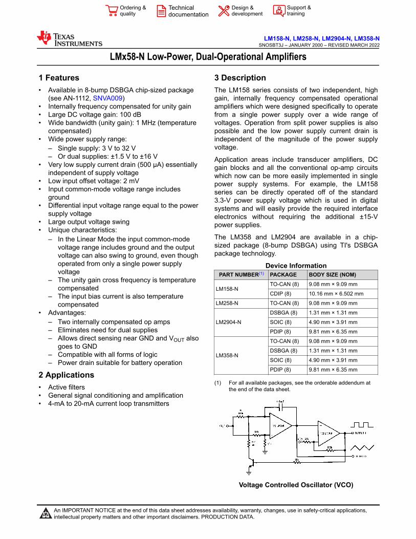
Voltage Controlled Oscillator (VCO)
LM158-N, LM258-N, LM2904-N, LM358-NSNOSBT3J – JANUARY 2000 – REVISED MARCH 2022
An IMPORTANT NOTICE at the end of this data sheet addresses availability, warranty, changes, use in safety-critical applications, intellectual property matters and other important disclaimers. PRODUCTION DATA.
Table of Contents1 Features............................................................................12 Applications..................................................................... 13 Description.......................................................................14 Revision History.............................................................. 25 Pin Configuration and Functions...................................36 Specifications.................................................................. 4
6.1 Absolute Maximum Ratings........................................ 46.2 ESD Ratings............................................................... 46.3 Recommended Operating Conditions.........................56.4 Thermal Information....................................................56.5 Electrical Characteristics: LM158A, LM358A,
LM158, LM258.............................................................. 56.6 Electrical Characteristics: LM358, LM2904.................76.7 Typical Characteristics................................................ 9
7 Detailed Description......................................................127.1 Overview................................................................... 127.2 Functional Block Diagram......................................... 12
7.3 Feature Description...................................................127.4 Device Functional Modes..........................................13
8 Application and Implementation.................................. 148.1 Application Information............................................. 148.2 Typical Applications.................................................. 14
9 Power Supply Recommendations................................2110 Layout...........................................................................21
10.1 Layout Guidelines................................................... 2110.2 Layout Example...................................................... 21
11 Device and Documentation Support..........................2211.1 Receiving Notification of Documentation Updates.. 2211.2 Support Resources................................................. 2211.3 Trademarks............................................................. 2211.4 Electrostatic Discharge Caution.............................. 2211.5 Glossary.................................................................. 22
12 Mechanical, Packaging, and Orderable Information.................................................................... 22
4 Revision HistoryNOTE: Page numbers for previous revisions may differ from page numbers in the current version.
Changes from Revision I (December 2014) to Revision J (March 2022) Page• Updated the numbering format for tables, figures, and cross-references throughout the document..................1• Corrected pin 5 (+INB) and pin 7 (OUTB) description information in the Pin Configuration and Functions
section................................................................................................................................................................ 3• Deleted Related Links from the Device and Documentation Support section.................................................. 22
Changes from Revision H (March 2013) to Revision I (December 2014) Page• Added Pin Configuration and Functions section, ESD Ratings table, Feature Description section, Device
Functional Modes, Application and Implementation section, Power Supply Recommendations section, Layout section, Device and Documentation Support section, and Mechanical, Packaging, and Orderable Information section ............................................................................................................................................................... 1
Changes from Revision G (March 2013) to Revision H (March 2013) Page• Changed layout of National Data Sheet to TI format.......................................................................................... 1
LM158-N, LM258-N, LM2904-N, LM358-NSNOSBT3J – JANUARY 2000 – REVISED MARCH 2022 www.ti.com
2 Submit Document Feedback Copyright © 2022 Texas Instruments Incorporated
Product Folder Links: LM158-N LM258-N LM2904-N LM358-N
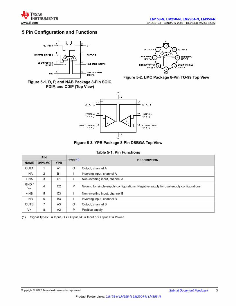
5 Pin Configuration and Functions
Figure 5-1. D, P, and NAB Package 8-Pin SOIC, PDIP, and CDIP (Top View)
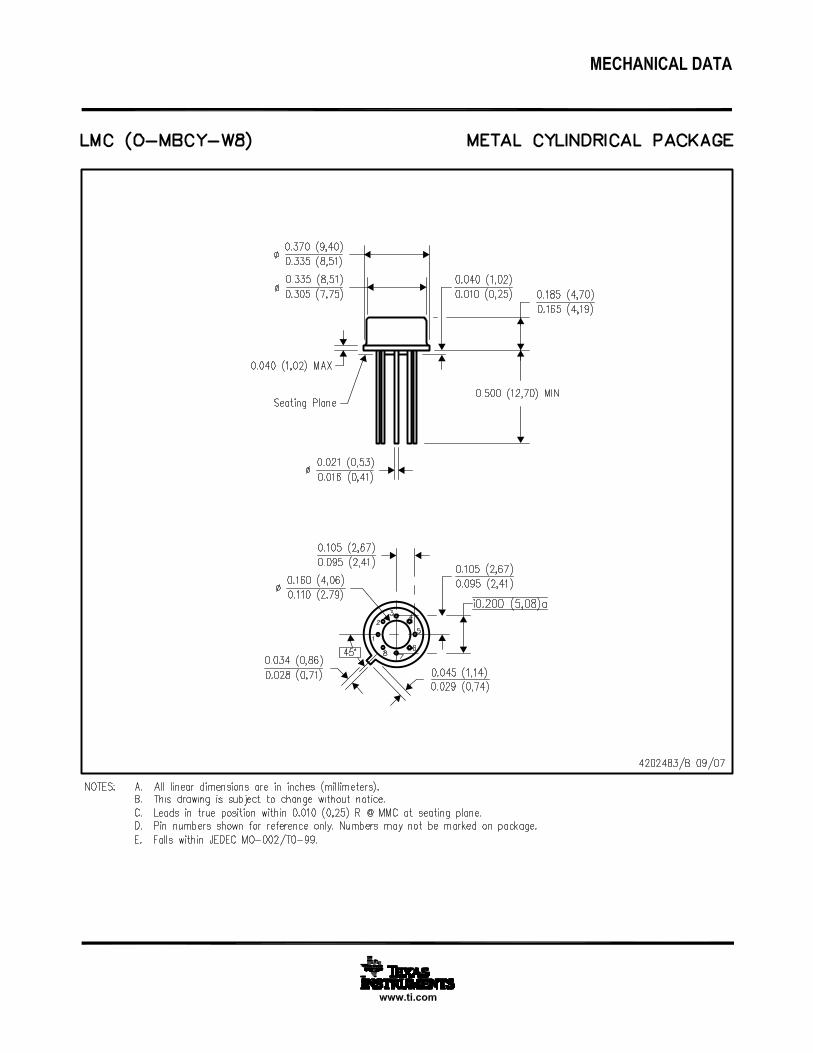
Figure 5-2. LMC Package 8-Pin TO-99 Top View
Figure 5-3. YPB Package 8-Pin DSBGA Top View
Table 5-1. Pin FunctionsPIN
TYPE(1) DESCRIPTIONNAME D/P/LMC YPBOUTA 1 A1 O Output, channel A
–INA 2 B1 I Inverting input, channel A
+INA 3 C1 I Non-inverting input, channel A
GND / V– 4 C2 P Ground for single-supply configurations. Negative supply for dual-supply configurations.
+INB 5 C3 I Non-inverting input, channel B
–INB 6 B3 I Inverting input, channel B
OUTB 7 A3 O Output, channel B
V+ 8 A2 P Positive supply
(1) Signal Types: I = Input, O = Output, I/O = Input or Output, P = Power
www.ti.comLM158-N, LM258-N, LM2904-N, LM358-N
SNOSBT3J – JANUARY 2000 – REVISED MARCH 2022
Copyright © 2022 Texas Instruments Incorporated Submit Document Feedback 3
Product Folder Links: LM158-N LM258-N LM2904-N LM358-N
6 Specifications6.1 Absolute Maximum RatingsSee (1) (2) (3).
LM158, LM258, LM358, LM158A, LM258A, LM358A
LM2904UNIT
MIN MAX MIN MAXSupply Voltage, V+ 32 26 V
Differential Input Voltage 32 26 V
Input Voltage −0.3 32 −0.3 26 V
Power Dissipation(4) PDIP (P) 830 830 mW
TO-99 (LMC) 550 mW
SOIC (D) 530 530 mW
DSBGA (YPB) 435 mW
Output Short-Circuit to GND (One Amplifier)(5)
V+ ≤ 15 V and TA = 25°C Continuous Continuous
Input Current (VIN < −0.3V)(6) 50 50 mA
Temperature −55 125 °C
PDIP Package (P): Soldering (10 seconds) 260 260 °C
SOIC Package (D) Vapor Phase (60 seconds)
215 215 °C
Infrared (15 seconds) 220 220 °C
Lead Temperature PDIP (P): (Soldering, 10 seconds) 260 260 °C
TO-99 (LMC): (Soldering, 10 seconds) 300 300 °C
Storage temperature, Tstg −65 150 −65 150 °C
(1) Absolute Maximum Ratings indicate limits beyond which damage to the device may occur. Recommended Operating Conditions indicate conditions for which the device is intended to be functional, but specific performance is not ensured. For ensured specifications and the test conditions, see the Electrical Characteristics.
(2) Refer to RETS158AX for LM158A military specifications and to RETS158X for LM158 military specifications.(3) If Military/Aerospace specified devices are required, please contact the TI Sales Office/Distributors for availability and specifications.(4) For operating at high temperatures, the LM358/LM358A, LM2904 must be derated based on a 125°C maximum junction temperature
and a thermal resistance of 120°C/W for PDIP, 182°C/W for TO-99, 189°C/W for SOIC package, and 230°C/W for DSBGA, which applies for the device soldered in a printed circuit board, operating in a still air ambient. The LM258/LM258A and LM158/LM158A can be derated based on a +150°C maximum junction temperature. The dissipation is the total of both amplifiers—use external resistors, where possible, to allow the amplifier to saturate or to reduce the power which is dissipated in the integrated circuit.
(5) Short circuits from the output to V+ can cause excessive heating and eventual destruction. When considering short circuits to ground, the maximum output current is approximately 40 mA independent of the magnitude of V+. At values of supply voltage in excess of +15 V, continuous short-circuits can exceed the power dissipation ratings and cause eventual destruction. Destructive dissipation can result from simultaneous shorts on all amplifiers.
(6) This input current will only exist when the voltage at any of the input leads is driven negative. It is due to the collector-base junction of the input PNP transistors becoming forward biased and thereby acting as input diode clamps. In addition to this diode action, there is also lateral NPN parasitic transistor action on the IC chip. This transistor action can cause the output voltages of the op amps to go to the V+voltage level (or to ground for a large overdrive) for the time duration that an input is driven negative. This is not destructive and normal output states will re-establish when the input voltage, which was negative, again returns to a value greater than −0.3 V (at 25°C).
6.2 ESD RatingsVALUE UNIT
V(ESD) Electrostatic discharge Human-body model (HBM), per ANSI/ESDA/JEDEC JS-001(1) ±250 V
(1) JEDEC document JEP155 states that 500-V HBM allows safe manufacturing with a standard ESD control process.
LM158-N, LM258-N, LM2904-N, LM358-NSNOSBT3J – JANUARY 2000 – REVISED MARCH 2022 www.ti.com
4 Submit Document Feedback Copyright © 2022 Texas Instruments Incorporated
Product Folder Links: LM158-N LM258-N LM2904-N LM358-N
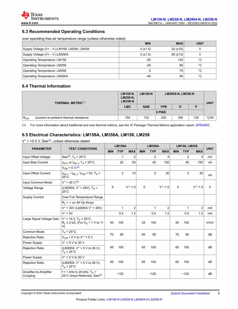
6.3 Recommended Operating Conditionsover operating free-air temperature range (unless otherwise noted)
MIN MAX UNITSupply Voltage (V+ - V-):LM158. LM258, LM358 3 (±1.5) 32 (±16) V
Supply Voltage (V+ - V-):LM2904 3 (±1.5) 26 (±13) V
Operating Temperature: LM158 -55 125 °C
Operating Temperature: LM258 -25 85 °C
Operating Temperature: LM358 0 70 °C
Operating Temperature: LM2904 -40 85 °C
6.4 Thermal Information
THERMAL METRIC(1)
LM158-N, LM258-N, LM358-N
LM158-N LM2904-N, LM358-N
UNITLMC NAB YPB D P
8 PINSRθJA Junction-to-ambient thermal resistance 155 132 230 189 120 °C/W
(1) For more information about traditional and new thermal metrics, see the IC Package Thermal Metrics application report, SPRA953.
6.5 Electrical Characteristics: LM158A, LM358A, LM158, LM258V+ = +5.0 V, See(2), unless otherwise stated
PARAMETER TEST CONDITIONSLM158A LM358A LM158, LM258
UNITMIN TYP MAX MIN TYP MAX MIN TYP MAX
Input Offset Voltage See(3), TA = 25°C 1 2 2 3 2 5 mV
Input Bias Current IIN(+) or IIN(−), TA = 25°C, 20 50 45 100 45 150 nA
VCM = 0 V,(4)
Input Offset Current IIN(+) − IIN(−), VCM = 0V, TA = 25°C
2 10 5 30 3 30 nA
Input Common-Mode V+ = 30 V,(5)
0 V+−1.5 0 V+−1.5 0 V+−1.5 VVoltage Range (LM2904, V+ = 26V), TA = 25°C
Supply Current Over Full Temperature Range
RL = ∞ on All Op Amps
V+ = 30V (LM2904 V+ = 26V) 1 2 1 2 1 2 mA
V+ = 5V 0.5 1.2 0.5 1.2 0.5 1.2 mA
Large Signal Voltage Gain V+ = 15 V, TA = 25°C,RL ≥ 2 kΩ, (For VO = 1 V to 11 V)
50 100 25 100 50 100 V/mV
Common-Mode TA = 25°C,70 85 65 85 70 85 dB
Rejection Ratio VCM = 0 V to V+−1.5 V
Power Supply V+ = 5 V to 30 V65 100 65 100 65 100 dBRejection Ratio (LM2904, V+ = 5 V to 26 V),
TA = 25°C
Power Supply V+ = 5 V to 30 V65 100 65 100 65 100 dBRejection Ratio (LM2904, V+ = 5 V to 26 V),
TA = 25°C
Amplifier-to-Amplifier Coupling
f = 1 kHz to 20 kHz, TA = 25°C (Input Referred), See(6) −120 −120 −120 dB
www.ti.comLM158-N, LM258-N, LM2904-N, LM358-N
SNOSBT3J – JANUARY 2000 – REVISED MARCH 2022
Copyright © 2022 Texas Instruments Incorporated Submit Document Feedback 5
Product Folder Links: LM158-N LM258-N LM2904-N LM358-N
6.5 Electrical Characteristics: LM158A, LM358A, LM158, LM258 (continued)V+ = +5.0 V, See(2), unless otherwise stated
PARAMETER TEST CONDITIONSLM158A LM358A LM158, LM258
UNITMIN TYP MAX MIN TYP MAX MIN TYP MAX
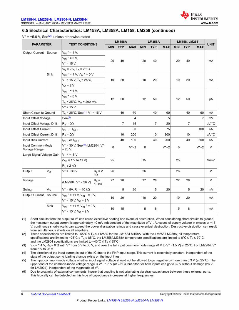
Output Current Source VIN + = 1 V,
20 40 20 40 20 40 mAVIN − = 0 V,
V+ = 15 V,
VO = 2 V, TA = 25°C
Sink VIN − = 1 V, VIN + = 0 V
10 20 10 20 10 20 mAV+ = 15 V, TA = 25°C,
VO = 2 V
VIN − = 1 V,
12 50 12 50 12 50 μAVIN + = 0 V
TA = 25°C, VO = 200 mV,
V+ = 15 V
Short Circuit to Ground TA = 25°C, See(1), V+ = 15 V 40 60 40 60 40 60 mA
Input Offset Voltage See(3) 4 5 7 mV
Input Offset Voltage Drift RS = 0Ω 7 15 7 20 7 μV/°C
Input Offset Current IIN(+) − IIN(−) 30 75 100 nA
Input Offset Current Drift RS = 0Ω 10 200 10 300 10 pA/°C
Input Bias Current IIN(+) or IIN(−) 40 100 40 200 40 300 nA
Input Common-ModeVoltage Range
V+ = 30 V, See(5) (LM2904, V+
= 26 V) 0 V+−2 0 V+−2 0 V+−2 V
Large Signal Voltage Gain V+ = +15 V
25 15 25 V/mV(VO = 1 V to 11 V)
RL ≥ 2 kΩ
Output VOH V+ = +30 V RL = 2 kΩ
26 26 26 V
Voltage (LM2904, V+ = 26 V) RL = 10 kΩ
27 28 27 28 27 28 V
Swing VOL V+ = 5V, RL = 10 kΩ 5 20 5 20 5 20 mV
Output Current Source VIN + = +1 V, VIN − = 0 V,10 20 10 20 10 20 mA
V+ = 15 V, VO = 2 V
Sink VIN − = +1 V, VIN + = 0 V,10 15 5 8 5 8 mA
V+ = 15 V, VO = 2 V
(1) Short circuits from the output to V+ can cause excessive heating and eventual destruction. When considering short circuits to ground, the maximum output current is approximately 40 mA independent of the magnitude of V+. At values of supply voltage in excess of +15 V, continuous short-circuits can exceed the power dissipation ratings and cause eventual destruction. Destructive dissipation can result from simultaneous shorts on all amplifiers.
(2) These specifications are limited to –55°C ≤ TA ≤ +125°C for the LM158/LM158A. With the LM258/LM258A, all temperature specifications are limited to −25°C ≤ TA ≤ 85°C, the LM358/LM358A temperature specifications are limited to 0°C ≤ TA ≤ 70°C, and the LM2904 specifications are limited to –40°C ≤ TA ≤ 85°C.
(3) VO ≃ 1.4 V, RS = 0 Ω with V+ from 5 V to 30 V; and over the full input common-mode range (0 V to V+ −1.5 V) at 25°C. For LM2904, V+
from 5 V to 26 V.(4) The direction of the input current is out of the IC due to the PNP input stage. This current is essentially constant, independent of the
state of the output so no loading change exists on the input lines.(5) The input common-mode voltage of either input signal voltage should not be allowed to go negative by more than 0.3 V (at 25°C). The
upper end of the common-mode voltage range is V+ −1.5 V (at 25°C), but either or both inputs can go to 32 V without damage (26 V for LM2904), independent of the magnitude of V+.
(6) Due to proximity of external components, insure that coupling is not originating via stray capacitance between these external parts. This typically can be detected as this type of capacitance increases at higher frequencies.
LM158-N, LM258-N, LM2904-N, LM358-NSNOSBT3J – JANUARY 2000 – REVISED MARCH 2022 www.ti.com
6 Submit Document Feedback Copyright © 2022 Texas Instruments Incorporated
Product Folder Links: LM158-N LM258-N LM2904-N LM358-N

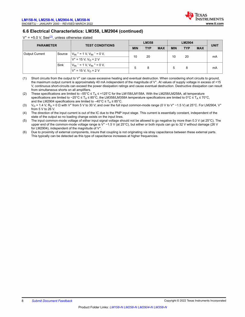
6.6 Electrical Characteristics: LM358, LM2904V+ = +5.0 V, See(2), unless otherwise stated
PARAMETER TEST CONDITIONSLM358 LM2904
UNITMIN TYP MAX MIN TYP MAX
Input Offset Voltage See(3) , TA = 25°C 2 7 2 7 mV
Input Bias Current IIN(+) or IIN(−), TA = 25°C,VCM = 0 V, See(4) 45 250 45 250 nA
Input Offset Current IIN(+) − IIN(−), VCM = 0 V, TA = 25°C 5 50 5 50 nA
Input Common-ModeVoltage Range
V+ = 30 V, See(5)
(LM2904, V+ = 26 V), TA = 25°C 0 V+−1.5 0 V+−1.5 V
Supply Current Over Full Temperature Range
RL = ∞ on All Op Amps
V+ = 30 V (LM2904 V+ = 26 V) 1 2 1 2 mA
V+ = 5 V 0.5 1.2 0.5 1.2 mA
Large Signal Voltage V+ = 15V, TA = 25°C,
Gain RL ≥ 2 kΩ, (For VO = 1 V to 11 V) 25 100 25 100 V/mV
Common-ModeRejection Ratio
TA = 25°C,65 85 50 70 dB
VCM = 0 V to V+−1.5 V
Power SupplyRejection Ratio
V+ = 5 V to 30 V 65 100 50 100 dB
(LM2904, V+ = 5 V to 26 V), TA = 25°C
Amplifier-to-Amplifier Coupling f = 1 kHz to 20 kHz, TA = 25°C(Input Referred), See(6) −120 −120 dB
Output Current Source VIN + = 1 V,
20 40 20 40 mAVIN − = 0 V,
V+ = 15 V,
VO = 2 V, TA = 25°C
Sink VIN − = 1 V, VIN + = 0 V
10 20 10 20 mAV+ = 15V, TA = 25°C,
VO = 2 V
VIN − = 1 V,
12 50 12 50 μAVIN + = 0 V
TA = 25°C, VO = 200 mV,
V+ = 15 V
Short Circuit to Ground TA = 25°C, See(1), V+ = 15 V 40 60 40 60 mA
Input Offset Voltage See(3) 9 10 mV
Input Offset Voltage Drift RS = 0 Ω 7 7 μV/°C
Input Offset Current IIN(+) − IIN(−) 150 45 200 nA
Input Offset Current Drift RS = 0 Ω 10 10 pA/°C
Input Bias Current IIN(+) or IIN(−) 40 500 40 500 nA
Input Common-ModeVoltage Range
V+ = 30 V, See(5) (LM2904, V+ = 26 V) 0 V+−2 0 V+ −2 V
Large Signal Voltage Gain V+ = +15 V
15 15 V/mV(VO = 1 V to 11 V)
RL ≥ 2 kΩ
Output VOH V+ = 30 V RL = 2 kΩ 26 22 V
Voltage (LM2904, V+ = 26 V) RL = 10 kΩ 27 28 23 24 V
Swing VOL V+ = 5 V, RL = 10 kΩ 5 20 5 100 mV
www.ti.comLM158-N, LM258-N, LM2904-N, LM358-N
SNOSBT3J – JANUARY 2000 – REVISED MARCH 2022
Copyright © 2022 Texas Instruments Incorporated Submit Document Feedback 7
Product Folder Links: LM158-N LM258-N LM2904-N LM358-N
6.6 Electrical Characteristics: LM358, LM2904 (continued)V+ = +5.0 V, See(2), unless otherwise stated
PARAMETER TEST CONDITIONSLM358 LM2904
UNITMIN TYP MAX MIN TYP MAX
Output Current Source VIN + = 1 V, VIN − = 0 V,10 20 10 20 mA
V+ = 15 V, VO = 2 V
Sink VIN − = 1 V, VIN + = 0 V,5 8 5 8 mA
V+ = 15 V, VO = 2 V
(1) Short circuits from the output to V+ can cause excessive heating and eventual destruction. When considering short circuits to ground, the maximum output current is approximately 40 mA independent of the magnitude of V+. At values of supply voltage in excess of +15 V, continuous short-circuits can exceed the power dissipation ratings and cause eventual destruction. Destructive dissipation can result from simultaneous shorts on all amplifiers.
(2) These specifications are limited to –55°C ≤ TA ≤ +125°C for the LM158/LM158A. With the LM258/LM258A, all temperature specifications are limited to −25°C ≤ TA ≤ 85°C, the LM358/LM358A temperature specifications are limited to 0°C ≤ TA ≤ 70°C, and the LM2904 specifications are limited to –40°C ≤ TA ≤ 85°C.
(3) VO ≃ 1.4 V, RS = 0 Ω with V+ from 5 V to 30 V; and over the full input common-mode range (0 V to V+ −1.5 V) at 25°C. For LM2904, V+
from 5 V to 26 V.(4) The direction of the input current is out of the IC due to the PNP input stage. This current is essentially constant, independent of the
state of the output so no loading change exists on the input lines.(5) The input common-mode voltage of either input signal voltage should not be allowed to go negative by more than 0.3 V (at 25°C). The
upper end of the common-mode voltage range is V+ −1.5 V (at 25°C), but either or both inputs can go to 32 V without damage (26 V for LM2904), independent of the magnitude of V+.
(6) Due to proximity of external components, insure that coupling is not originating via stray capacitance between these external parts. This typically can be detected as this type of capacitance increases at higher frequencies.
LM158-N, LM258-N, LM2904-N, LM358-NSNOSBT3J – JANUARY 2000 – REVISED MARCH 2022 www.ti.com
8 Submit Document Feedback Copyright © 2022 Texas Instruments Incorporated
Product Folder Links: LM158-N LM258-N LM2904-N LM358-N
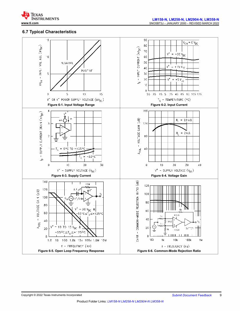
6.7 Typical Characteristics
Figure 6-1. Input Voltage Range Figure 6-2. Input Current
Figure 6-3. Supply Current Figure 6-4. Voltage Gain
Figure 6-5. Open Loop Frequency Response Figure 6-6. Common-Mode Rejection Ratio
www.ti.comLM158-N, LM258-N, LM2904-N, LM358-N
SNOSBT3J – JANUARY 2000 – REVISED MARCH 2022
Copyright © 2022 Texas Instruments Incorporated Submit Document Feedback 9
Product Folder Links: LM158-N LM258-N LM2904-N LM358-N
6.7 Typical Characteristics (continued)
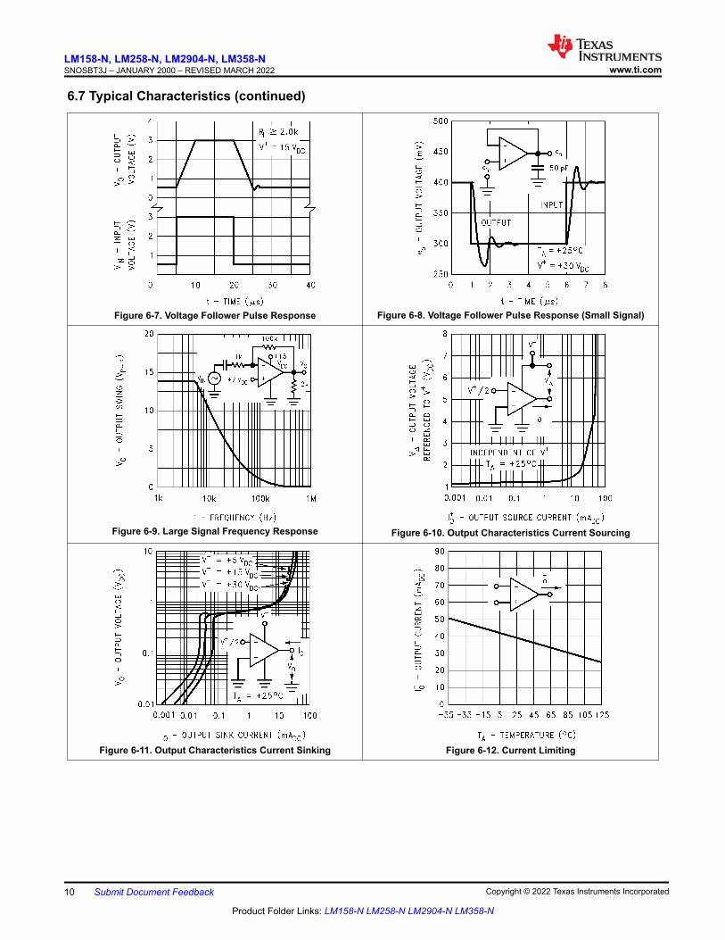
Figure 6-7. Voltage Follower Pulse Response Figure 6-8. Voltage Follower Pulse Response (Small Signal)
Figure 6-9. Large Signal Frequency Response Figure 6-10. Output Characteristics Current Sourcing
Figure 6-11. Output Characteristics Current Sinking Figure 6-12. Current Limiting
LM158-N, LM258-N, LM2904-N, LM358-NSNOSBT3J – JANUARY 2000 – REVISED MARCH 2022 www.ti.com
10 Submit Document Feedback Copyright © 2022 Texas Instruments Incorporated
Product Folder Links: LM158-N LM258-N LM2904-N LM358-N
6.7 Typical Characteristics (continued)
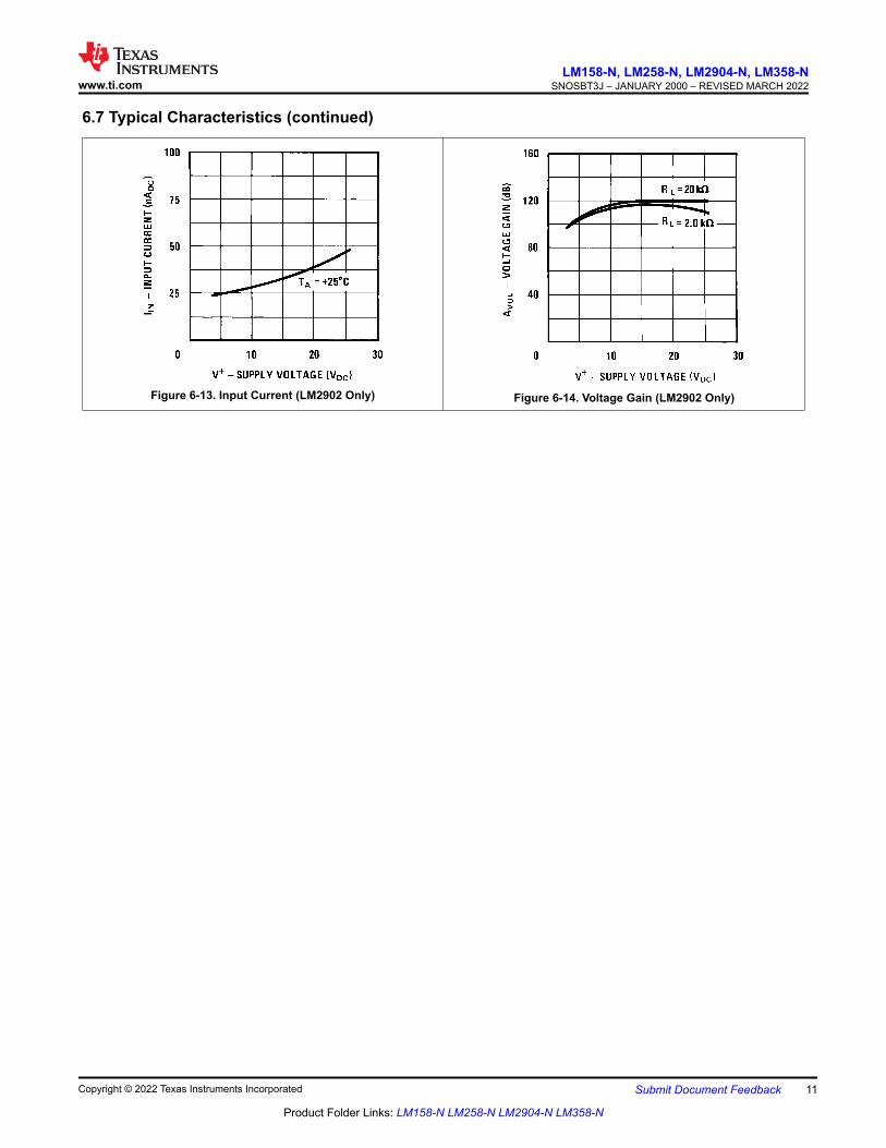
Figure 6-13. Input Current (LM2902 Only) Figure 6-14. Voltage Gain (LM2902 Only)
www.ti.comLM158-N, LM258-N, LM2904-N, LM358-N
SNOSBT3J – JANUARY 2000 – REVISED MARCH 2022
Copyright © 2022 Texas Instruments Incorporated Submit Document Feedback 11
Product Folder Links: LM158-N LM258-N LM2904-N LM358-N
7 Detailed Description7.1 OverviewThe LM158 series are operational amplifiers which can operate with only a single power supply voltage, have true-differential inputs, and remain in the linear mode with an input common-mode voltage of 0 VDC. These amplifiers operate over a wide range of power supply voltage with little change in performance characteristics. At 25°C amplifier operation is possible down to a minimum supply voltage of 2.3 VDC.
Large differential input voltages can be easily accommodated and, as input differential voltage protection diodes are not needed, no large input currents result from large differential input voltages. The differential input voltage may be larger than V+ without damaging the device. Protection should be provided to prevent the input voltages from going negative more than −0.3 VDC (at 25°C). An input clamp diode with a resistor to the IC input terminal can be used.
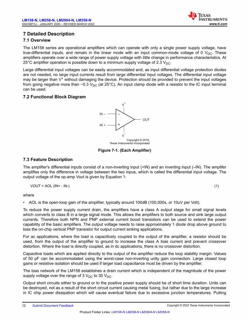
7.2 Functional Block Diagram
_
+OUT
V+
V–
IN –
IN +
Copyright © 2016,Texas Instruments Incorporated
Figure 7-1. (Each Amplifier)
7.3 Feature DescriptionThe amplifier's differential inputs consist of a non-inverting input (+IN) and an inverting input (–IN). The amplifer amplifies only the difference in voltage between the two inpus, which is called the differential input voltage. The output voltage of the op-amp Vout is given by Equation 1:
VOUT = AOL (IN+ - IN-) (1)
where
• AOL is the open-loop gain of the amplifier, typically around 100dB (100,000x, or 10uV per Volt).
To reduce the power supply current drain, the amplifiers have a class A output stage for small signal levels which converts to class B in a large signal mode. This allows the amplifiers to both source and sink large output currents. Therefore both NPN and PNP external current boost transistors can be used to extend the power capability of the basic amplifiers. The output voltage needs to raise approximately 1 diode drop above ground to bias the on-chip vertical PNP transistor for output current sinking applications.
For ac applications, where the load is capacitively coupled to the output of the amplifier, a resistor should be used, from the output of the amplifier to ground to increase the class A bias current and prevent crossover distortion. Where the load is directly coupled, as in dc applications, there is no crossover distortion.
Capacitive loads which are applied directly to the output of the amplifier reduce the loop stability margin. Values of 50 pF can be accommodated using the worst-case non-inverting unity gain connection. Large closed loop gains or resistive isolation should be used if larger load capacitance must be driven by the amplifier.
The bias network of the LM158 establishes a drain current which is independent of the magnitude of the power supply voltage over the range of 3 VDC to 30 VDC.
Output short circuits either to ground or to the positive power supply should be of short time duration. Units can be destroyed, not as a result of the short circuit current causing metal fusing, but rather due to the large increase in IC chip power dissipation which will cause eventual failure due to excessive junction temperatures. Putting
LM158-N, LM258-N, LM2904-N, LM358-NSNOSBT3J – JANUARY 2000 – REVISED MARCH 2022 www.ti.com
12 Submit Document Feedback Copyright © 2022 Texas Instruments Incorporated
Product Folder Links: LM158-N LM258-N LM2904-N LM358-N

direct short-circuits on more than one amplifier at a time will increase the total IC power dissipation to destructive levels, if not properly protected with external dissipation limiting resistors in series with the output leads of the amplifiers. The larger value of output source current which is available at 25°C provides a larger output current capability at elevated temperatures (see Typical Characteristics) than a standard IC op amp.
7.4 Device Functional Modes
Figure 7-2. Schematic Diagram
The circuits presented in the Typical Single-Supply Applications emphasize operation on only a single power supply voltage. If complementary power supplies are available, all of the standard op-amp circuits can be used. In general, introducing a pseudo-ground (a bias voltage reference of V+/2) will allow operation above and below this value in single power supply systems. Many application circuits are shown which take advantage of the wide input common-mode voltage range which includes ground. In most cases, input biasing is not required and input voltages which range to ground can easily be accommodated.
www.ti.comLM158-N, LM258-N, LM2904-N, LM358-N
SNOSBT3J – JANUARY 2000 – REVISED MARCH 2022
Copyright © 2022 Texas Instruments Incorporated Submit Document Feedback 13
Product Folder Links: LM158-N LM258-N LM2904-N LM358-N
8 Application and ImplementationNote
Information in the following applications sections is not part of the TI component specification, and TI does not warrant its accuracy or completeness. TI’s customers are responsible for determining suitability of components for their purposes. Customers should validate and test their design implementation to confirm system functionality.
8.1 Application InformationThe LM158 family bring performance, economy, and ease-of-use to a wide variety of op-amp applications.
8.2 Typical Applications8.2.1 Noninverting DC Gain
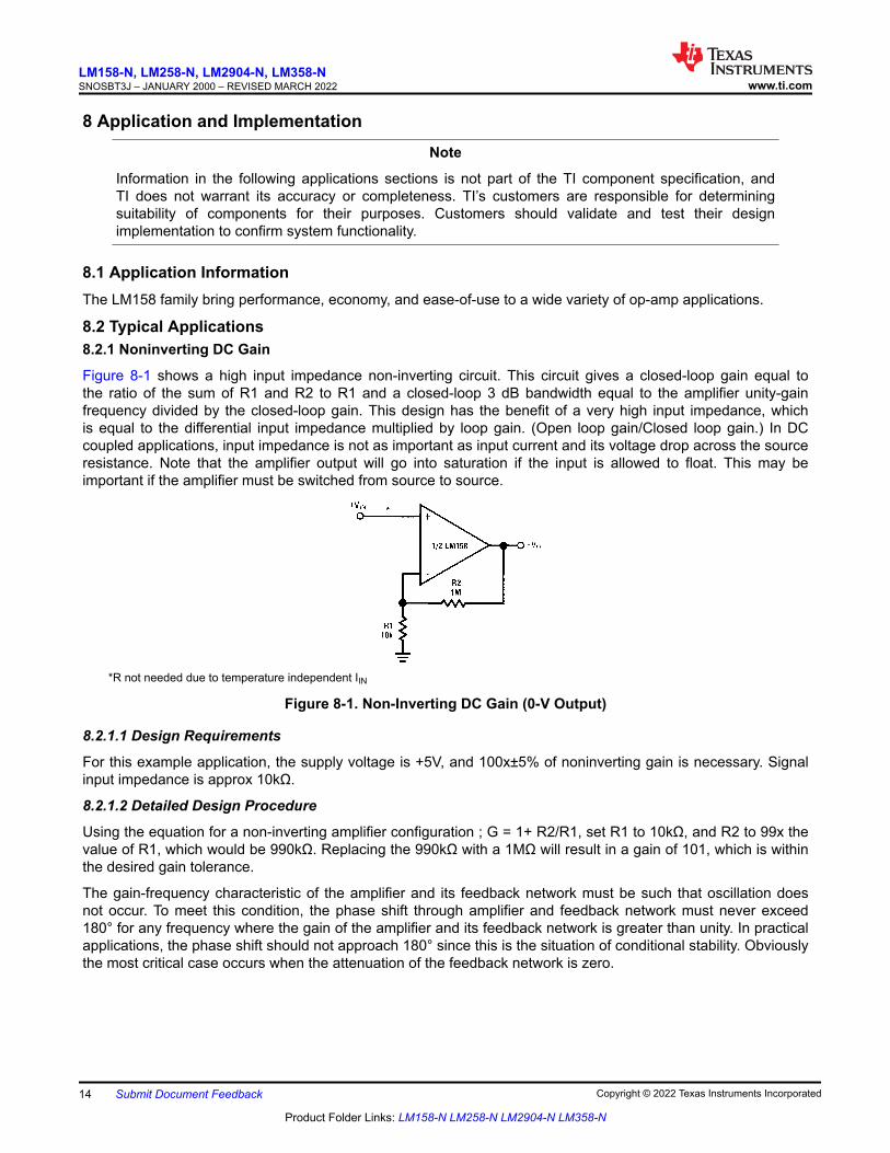
Figure 8-1 shows a high input impedance non-inverting circuit. This circuit gives a closed-loop gain equal to the ratio of the sum of R1 and R2 to R1 and a closed-loop 3 dB bandwidth equal to the amplifier unity-gain frequency divided by the closed-loop gain. This design has the benefit of a very high input impedance, which is equal to the differential input impedance multiplied by loop gain. (Open loop gain/Closed loop gain.) In DC coupled applications, input impedance is not as important as input current and its voltage drop across the source resistance. Note that the amplifier output will go into saturation if the input is allowed to float. This may be important if the amplifier must be switched from source to source.
*R not needed due to temperature independent IIN
Figure 8-1. Non-Inverting DC Gain (0-V Output)
8.2.1.1 Design Requirements
For this example application, the supply voltage is +5V, and 100x±5% of noninverting gain is necessary. Signal input impedance is approx 10kΩ.
8.2.1.2 Detailed Design Procedure
Using the equation for a non-inverting amplifier configuration ; G = 1+ R2/R1, set R1 to 10kΩ, and R2 to 99x the value of R1, which would be 990kΩ. Replacing the 990kΩ with a 1MΩ will result in a gain of 101, which is within the desired gain tolerance.
The gain-frequency characteristic of the amplifier and its feedback network must be such that oscillation does not occur. To meet this condition, the phase shift through amplifier and feedback network must never exceed 180° for any frequency where the gain of the amplifier and its feedback network is greater than unity. In practical applications, the phase shift should not approach 180° since this is the situation of conditional stability. Obviously the most critical case occurs when the attenuation of the feedback network is zero.
LM158-N, LM258-N, LM2904-N, LM358-NSNOSBT3J – JANUARY 2000 – REVISED MARCH 2022 www.ti.com
14 Submit Document Feedback Copyright © 2022 Texas Instruments Incorporated
Product Folder Links: LM158-N LM258-N LM2904-N LM358-N
8.2.1.3 Application Curve
Figure 8-2. Transfer Curve for Non-Inverting Configuration
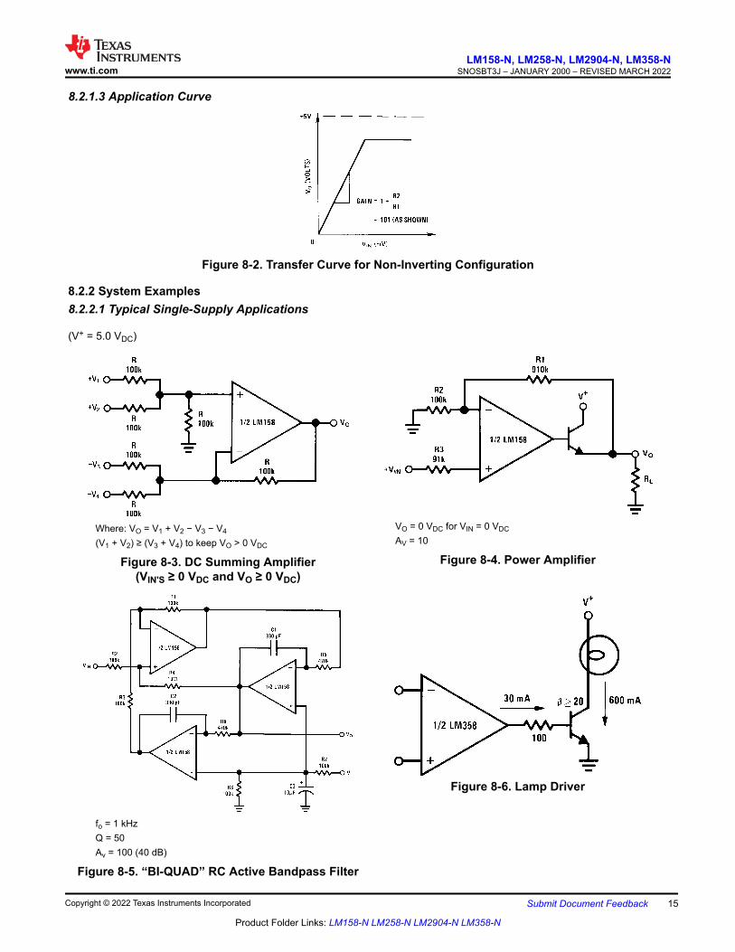
8.2.2 System Examples8.2.2.1 Typical Single-Supply Applications
(V+ = 5.0 VDC)
Where: VO = V1 + V2 − V3 − V4
(V1 + V2) ≥ (V3 + V4) to keep VO > 0 VDC
Figure 8-3. DC Summing Amplifier(VIN'S ≥ 0 VDC and VO ≥ 0 VDC)
VO = 0 VDC for VIN = 0 VDC
AV = 10
Figure 8-4. Power Amplifier
fo = 1 kHzQ = 50Av = 100 (40 dB)
Figure 8-5. “BI-QUAD” RC Active Bandpass Filter
Figure 8-6. Lamp Driver
www.ti.comLM158-N, LM258-N, LM2904-N, LM358-N
SNOSBT3J – JANUARY 2000 – REVISED MARCH 2022
Copyright © 2022 Texas Instruments Incorporated Submit Document Feedback 15
Product Folder Links: LM158-N LM258-N LM2904-N LM358-N
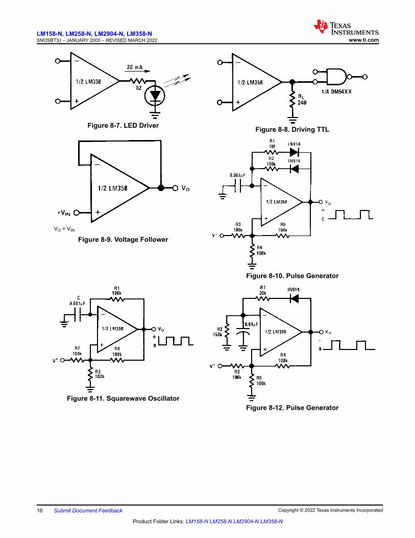
Figure 8-7. LED Driver Figure 8-8. Driving TTL
VO = VIN
Figure 8-9. Voltage Follower
Figure 8-10. Pulse Generator
Figure 8-11. Squarewave OscillatorFigure 8-12. Pulse Generator
LM158-N, LM258-N, LM2904-N, LM358-NSNOSBT3J – JANUARY 2000 – REVISED MARCH 2022 www.ti.com
16 Submit Document Feedback Copyright © 2022 Texas Instruments Incorporated
Product Folder Links: LM158-N LM258-N LM2904-N LM358-N
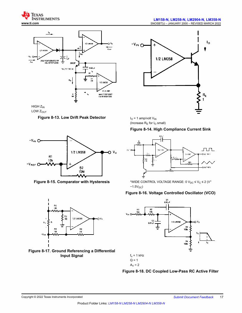
HIGH ZIN
LOW ZOUT
Figure 8-13. Low Drift Peak Detector IO = 1 amp/volt VIN
(Increase RE for IO small)
Figure 8-14. High Compliance Current Sink
Figure 8-15. Comparator with Hysteresis *WIDE CONTROL VOLTAGE RANGE: 0 VDC ≤ VC ≤ 2 (V+
−1.5VDC)
Figure 8-16. Voltage Controlled Oscillator (VCO)
Figure 8-17. Ground Referencing a Differential Input Signal fo = 1 kHz
Q = 1AV = 2
Figure 8-18. DC Coupled Low-Pass RC Active Filter
www.ti.comLM158-N, LM258-N, LM2904-N, LM358-N
SNOSBT3J – JANUARY 2000 – REVISED MARCH 2022
Copyright © 2022 Texas Instruments Incorporated Submit Document Feedback 17
Product Folder Links: LM158-N LM258-N LM2904-N LM358-N
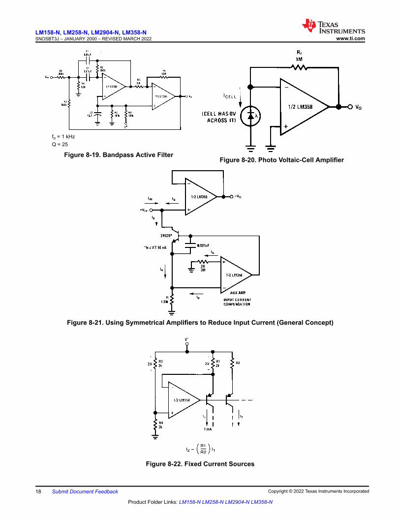
fo = 1 kHzQ = 25
Figure 8-19. Bandpass Active FilterFigure 8-20. Photo Voltaic-Cell Amplifier
Figure 8-21. Using Symmetrical Amplifiers to Reduce Input Current (General Concept)
Figure 8-22. Fixed Current Sources
LM158-N, LM258-N, LM2904-N, LM358-NSNOSBT3J – JANUARY 2000 – REVISED MARCH 2022 www.ti.com
18 Submit Document Feedback Copyright © 2022 Texas Instruments Incorporated
Product Folder Links: LM158-N LM258-N LM2904-N LM358-N
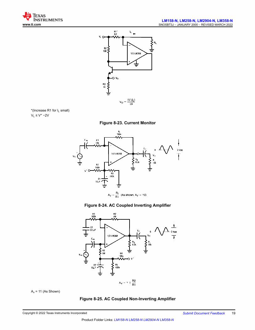
*(Increase R1 for IL small)VL ≤ V+ −2V
Figure 8-23. Current Monitor
Figure 8-24. AC Coupled Inverting Amplifier
Av = 11 (As Shown)
Figure 8-25. AC Coupled Non-Inverting Amplifier
www.ti.comLM158-N, LM258-N, LM2904-N, LM358-N
SNOSBT3J – JANUARY 2000 – REVISED MARCH 2022
Copyright © 2022 Texas Instruments Incorporated Submit Document Feedback 19
Product Folder Links: LM158-N LM258-N LM2904-N LM358-N
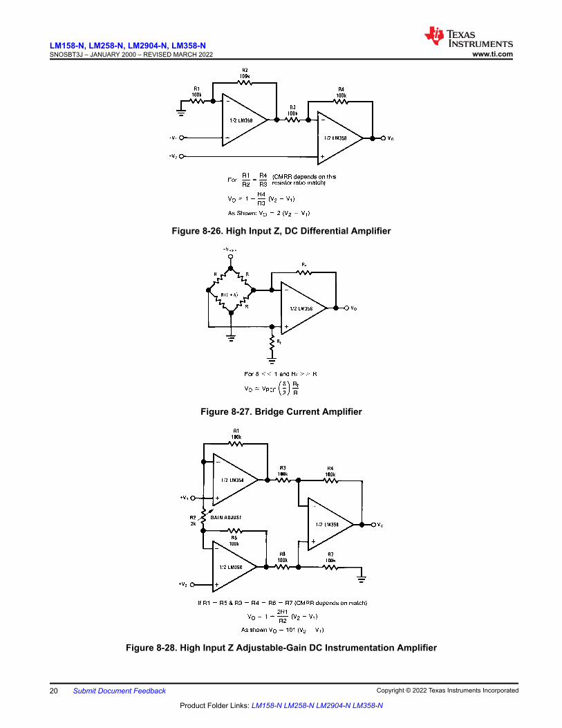
Figure 8-26. High Input Z, DC Differential Amplifier
Figure 8-27. Bridge Current Amplifier
Figure 8-28. High Input Z Adjustable-Gain DC Instrumentation Amplifier
LM158-N, LM258-N, LM2904-N, LM358-NSNOSBT3J – JANUARY 2000 – REVISED MARCH 2022 www.ti.com
20 Submit Document Feedback Copyright © 2022 Texas Instruments Incorporated
Product Folder Links: LM158-N LM258-N LM2904-N LM358-N
9 Power Supply RecommendationsFor proper operation, the power supplies must be properly decoupled. For decoupling the supply pins it is suggested that 10-nF capacitors be placed as close as possible to the op-amp power supply pins. For single supply, place a capacitor between V+ and V– supply leads. For dual supplies, place one capacitor between V+ and ground, and one capacitor between V– and ground.
Precautions should be taken to insure that the power supply for the integrated circuit never becomes reversed in polarity or that the unit is not inadvertently installed backwards in a test socket as an unlimited current surge through the resulting forward diode within the IC could cause fusing of the internal conductors and result in a destroyed unit.
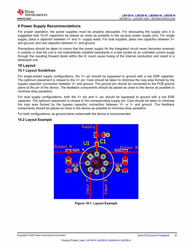
10 Layout10.1 Layout GuidelinesFor single-ended supply configurations, the V+ pin should be bypassed to ground with a low ESR capacitor. The optimum placement is closest to the V+ pin. Care should be taken to minimize the loop area formed by the bypass capacitor connection between V+ and ground. The ground pin should be connected to the PCB ground plane at the pin of the device. The feedback components should be placed as close to the device as possible to minimize stray parasitics.
For dual supply configurations, both the V+ pin and V- pin should be bypassed to ground with a low ESR capacitor. The optimum placement is closest to the corresponding supply pin. Care should be taken to minimize the loop area formed by the bypass capacitor connection between V+ or V- and ground. The feedback components should be placed as close to the device as possible to minimize stray parasitics.
For both configurations, as ground plane underneath the device is recommended.
10.2 Layout Example
Figure 10-1. Layout Example
www.ti.comLM158-N, LM258-N, LM2904-N, LM358-N
SNOSBT3J – JANUARY 2000 – REVISED MARCH 2022
Copyright © 2022 Texas Instruments Incorporated Submit Document Feedback 21
Product Folder Links: LM158-N LM258-N LM2904-N LM358-N
11 Device and Documentation Support11.1 Receiving Notification of Documentation UpdatesTo receive notification of documentation updates, navigate to the device product folder on ti.com. Click on Subscribe to updates to register and receive a weekly digest of any product information that has changed. For change details, review the revision history included in any revised document.
11.2 Support ResourcesTI E2E™ support forums are an engineer's go-to source for fast, verified answers and design help — straight from the experts. Search existing answers or ask your own question to get the quick design help you need.
Linked content is provided "AS IS" by the respective contributors. They do not constitute TI specifications and do not necessarily reflect TI's views; see TI's Terms of Use.
11.3 TrademarksTI E2E™ is a trademark of Texas Instruments.All trademarks are the property of their respective owners.11.4 Electrostatic Discharge Caution
This integrated circuit can be damaged by ESD. Texas Instruments recommends that all integrated circuits be handled with appropriate precautions. Failure to observe proper handling and installation procedures can cause damage.ESD damage can range from subtle performance degradation to complete device failure. Precision integrated circuits may be more susceptible to damage because very small parametric changes could cause the device not to meet its published specifications.
11.5 GlossaryTI Glossary This glossary lists and explains terms, acronyms, and definitions.
12 Mechanical, Packaging, and Orderable InformationThe following pages include mechanical, packaging, and orderable information. This information is the most current data available for the designated devices. This data is subject to change without notice and revision of this document. For browser-based versions of this data sheet, refer to the left-hand navigation.
LM158-N, LM258-N, LM2904-N, LM358-NSNOSBT3J – JANUARY 2000 – REVISED MARCH 2022 www.ti.com
22 Submit Document Feedback Copyright © 2022 Texas Instruments Incorporated
Product Folder Links: LM158-N LM258-N LM2904-N LM358-N

PACKAGE OPTION ADDENDUM
www.ti.com 27-May-2022
PACKAGING INFORMATION
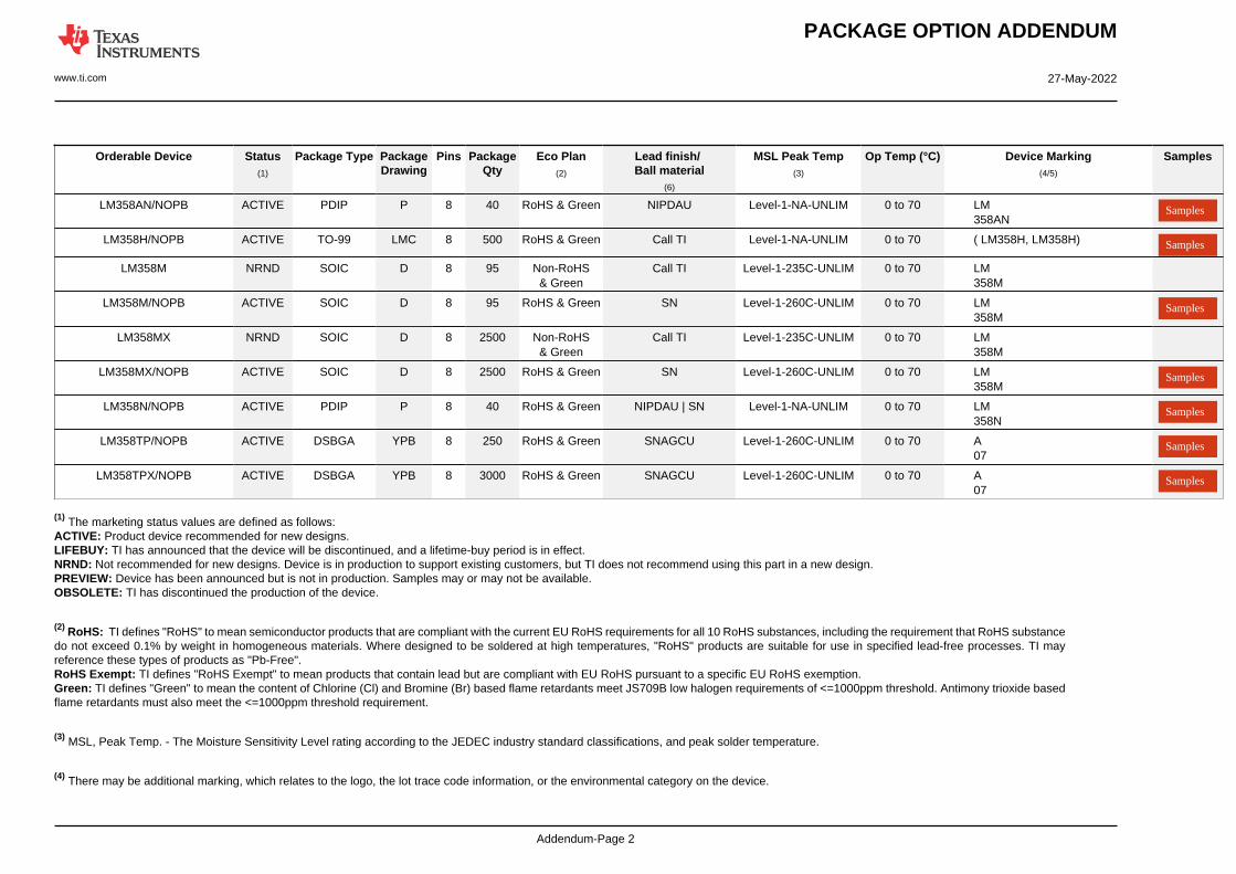
Orderable Device Status(1)
Package Type PackageDrawing
Pins PackageQty
Eco Plan(2)
Lead finish/Ball material
(6)
MSL Peak Temp(3)
Op Temp (°C) Device Marking(4/5)
Samples
LM158AH ACTIVE TO-99 LMC 8 500 Non-RoHS &Non-Green
Call TI Call TI -55 to 125 ( LM158AH, LM158AH )
Samples
LM158AH/NOPB ACTIVE TO-99 LMC 8 500 RoHS & Green Call TI Level-1-NA-UNLIM -55 to 125 ( LM158AH, LM158AH )
Samples
LM158H ACTIVE TO-99 LMC 8 500 Non-RoHS &Non-Green
Call TI Call TI -55 to 125 ( LM158H, LM158H) Samples
LM158H/NOPB ACTIVE TO-99 LMC 8 500 RoHS & Green Call TI Level-1-NA-UNLIM -55 to 125 ( LM158H, LM158H) Samples
LM158J ACTIVE CDIP NAB 8 40 Non-RoHS& Green
Call TI Level-1-NA-UNLIM -55 to 125 LM158J Samples
LM258H ACTIVE TO-99 LMC 8 500 Non-RoHS &Non-Green
Call TI Call TI -25 to 85 ( LM258H, LM258H) Samples
LM258H/NOPB ACTIVE TO-99 LMC 8 500 RoHS & Green Call TI Level-1-NA-UNLIM -25 to 85 ( LM258H, LM258H) Samples
LM2904ITP/NOPB ACTIVE DSBGA YPB 8 250 RoHS & Green SNAGCU Level-1-260C-UNLIM -40 to 85 A09
Samples
LM2904ITPX/NOPB ACTIVE DSBGA YPB 8 3000 RoHS & Green SNAGCU Level-1-260C-UNLIM -40 to 85 A09
Samples
LM2904M/NOPB ACTIVE SOIC D 8 95 RoHS & Green SN Level-1-260C-UNLIM -40 to 85 LM2904M
Samples
LM2904MX NRND SOIC D 8 2500 Non-RoHS& Green
Call TI Level-1-235C-UNLIM -40 to 85 LM2904M
LM2904MX/NOPB ACTIVE SOIC D 8 2500 RoHS & Green SN Level-1-260C-UNLIM -40 to 85 LM2904M
Samples
LM2904N/NOPB ACTIVE PDIP P 8 40 RoHS & Green NIPDAU | SN Level-1-NA-UNLIM -40 to 85 LM2904N
Samples
LM358AM NRND SOIC D 8 95 Non-RoHS& Green
Call TI Level-1-235C-UNLIM 0 to 70 LM358AM
LM358AM/NOPB ACTIVE SOIC D 8 95 RoHS & Green SN Level-1-260C-UNLIM 0 to 70 LM358AM
Samples
LM358AMX NRND SOIC D 8 2500 Non-RoHS& Green
Call TI Level-1-235C-UNLIM 0 to 70 LM358AM
LM358AMX/NOPB ACTIVE SOIC D 8 2500 RoHS & Green SN Level-1-260C-UNLIM 0 to 70 LM358AM
Samples
Addendum-Page 1
PACKAGE OPTION ADDENDUM
www.ti.com 27-May-2022
Orderable Device Status(1)
Package Type PackageDrawing
Pins PackageQty
Eco Plan(2)
Lead finish/Ball material
(6)
MSL Peak Temp(3)
Op Temp (°C) Device Marking(4/5)
Samples
LM358AN/NOPB ACTIVE PDIP P 8 40 RoHS & Green NIPDAU Level-1-NA-UNLIM 0 to 70 LM358AN
Samples
LM358H/NOPB ACTIVE TO-99 LMC 8 500 RoHS & Green Call TI Level-1-NA-UNLIM 0 to 70 ( LM358H, LM358H) Samples
LM358M NRND SOIC D 8 95 Non-RoHS& Green
Call TI Level-1-235C-UNLIM 0 to 70 LM358M
LM358M/NOPB ACTIVE SOIC D 8 95 RoHS & Green SN Level-1-260C-UNLIM 0 to 70 LM358M
Samples
LM358MX NRND SOIC D 8 2500 Non-RoHS& Green
Call TI Level-1-235C-UNLIM 0 to 70 LM358M
LM358MX/NOPB ACTIVE SOIC D 8 2500 RoHS & Green SN Level-1-260C-UNLIM 0 to 70 LM358M
Samples
LM358N/NOPB ACTIVE PDIP P 8 40 RoHS & Green NIPDAU | SN Level-1-NA-UNLIM 0 to 70 LM358N
Samples
LM358TP/NOPB ACTIVE DSBGA YPB 8 250 RoHS & Green SNAGCU Level-1-260C-UNLIM 0 to 70 A07
Samples
LM358TPX/NOPB ACTIVE DSBGA YPB 8 3000 RoHS & Green SNAGCU Level-1-260C-UNLIM 0 to 70 A07
Samples
(1) The marketing status values are defined as follows:ACTIVE: Product device recommended for new designs.LIFEBUY: TI has announced that the device will be discontinued, and a lifetime-buy period is in effect.NRND: Not recommended for new designs. Device is in production to support existing customers, but TI does not recommend using this part in a new design.PREVIEW: Device has been announced but is not in production. Samples may or may not be available.OBSOLETE: TI has discontinued the production of the device.
(2) RoHS: TI defines "RoHS" to mean semiconductor products that are compliant with the current EU RoHS requirements for all 10 RoHS substances, including the requirement that RoHS substancedo not exceed 0.1% by weight in homogeneous materials. Where designed to be soldered at high temperatures, "RoHS" products are suitable for use in specified lead-free processes. TI mayreference these types of products as "Pb-Free".RoHS Exempt: TI defines "RoHS Exempt" to mean products that contain lead but are compliant with EU RoHS pursuant to a specific EU RoHS exemption.Green: TI defines "Green" to mean the content of Chlorine (Cl) and Bromine (Br) based flame retardants meet JS709B low halogen requirements of <=1000ppm threshold. Antimony trioxide basedflame retardants must also meet the <=1000ppm threshold requirement.
(3) MSL, Peak Temp. - The Moisture Sensitivity Level rating according to the JEDEC industry standard classifications, and peak solder temperature.
(4) There may be additional marking, which relates to the logo, the lot trace code information, or the environmental category on the device.
Addendum-Page 2
PACKAGE OPTION ADDENDUM
www.ti.com 27-May-2022
(5) Multiple Device Markings will be inside parentheses. Only one Device Marking contained in parentheses and separated by a "~" will appear on a device. If a line is indented then it is a continuationof the previous line and the two combined represent the entire Device Marking for that device.
(6) Lead finish/Ball material - Orderable Devices may have multiple material finish options. Finish options are separated by a vertical ruled line. Lead finish/Ball material values may wrap to twolines if the finish value exceeds the maximum column width.
Important Information and Disclaimer:The information provided on this page represents TI's knowledge and belief as of the date that it is provided. TI bases its knowledge and belief on informationprovided by third parties, and makes no representation or warranty as to the accuracy of such information. Efforts are underway to better integrate information from third parties. TI has taken andcontinues to take reasonable steps to provide representative and accurate information but may not have conducted destructive testing or chemical analysis on incoming materials and chemicals.TI and TI suppliers consider certain information to be proprietary, and thus CAS numbers and other limited information may not be available for release.
In no event shall TI's liability arising out of such information exceed the total purchase price of the TI part(s) at issue in this document sold by TI to Customer on an annual basis.
OTHER QUALIFIED VERSIONS OF LM2904-N :
• Automotive : LM2904-Q1
• Enhanced Product : LM2904-EP
NOTE: Qualified Version Definitions:
• Automotive - Q100 devices qualified for high-reliability automotive applications targeting zero defects
• Enhanced Product - Supports Defense, Aerospace and Medical Applications
Addendum-Page 3
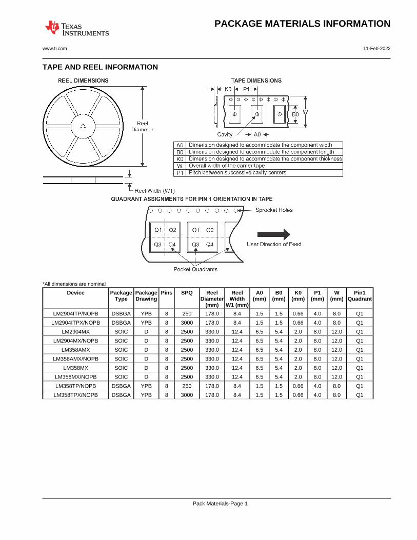
TAPE AND REEL INFORMATION
*All dimensions are nominal
Device PackageType
PackageDrawing
Pins SPQ ReelDiameter
(mm)
ReelWidth
W1 (mm)
A0(mm)
B0(mm)
K0(mm)
P1(mm)
W(mm)
Pin1Quadrant
LM2904ITP/NOPB DSBGA YPB 8 250 178.0 8.4 1.5 1.5 0.66 4.0 8.0 Q1
LM2904ITPX/NOPB DSBGA YPB 8 3000 178.0 8.4 1.5 1.5 0.66 4.0 8.0 Q1
LM2904MX SOIC D 8 2500 330.0 12.4 6.5 5.4 2.0 8.0 12.0 Q1
LM2904MX/NOPB SOIC D 8 2500 330.0 12.4 6.5 5.4 2.0 8.0 12.0 Q1
LM358AMX SOIC D 8 2500 330.0 12.4 6.5 5.4 2.0 8.0 12.0 Q1
LM358AMX/NOPB SOIC D 8 2500 330.0 12.4 6.5 5.4 2.0 8.0 12.0 Q1
LM358MX SOIC D 8 2500 330.0 12.4 6.5 5.4 2.0 8.0 12.0 Q1
LM358MX/NOPB SOIC D 8 2500 330.0 12.4 6.5 5.4 2.0 8.0 12.0 Q1
LM358TP/NOPB DSBGA YPB 8 250 178.0 8.4 1.5 1.5 0.66 4.0 8.0 Q1
LM358TPX/NOPB DSBGA YPB 8 3000 178.0 8.4 1.5 1.5 0.66 4.0 8.0 Q1
PACKAGE MATERIALS INFORMATION
www.ti.com 11-Feb-2022
Pack Materials-Page 1
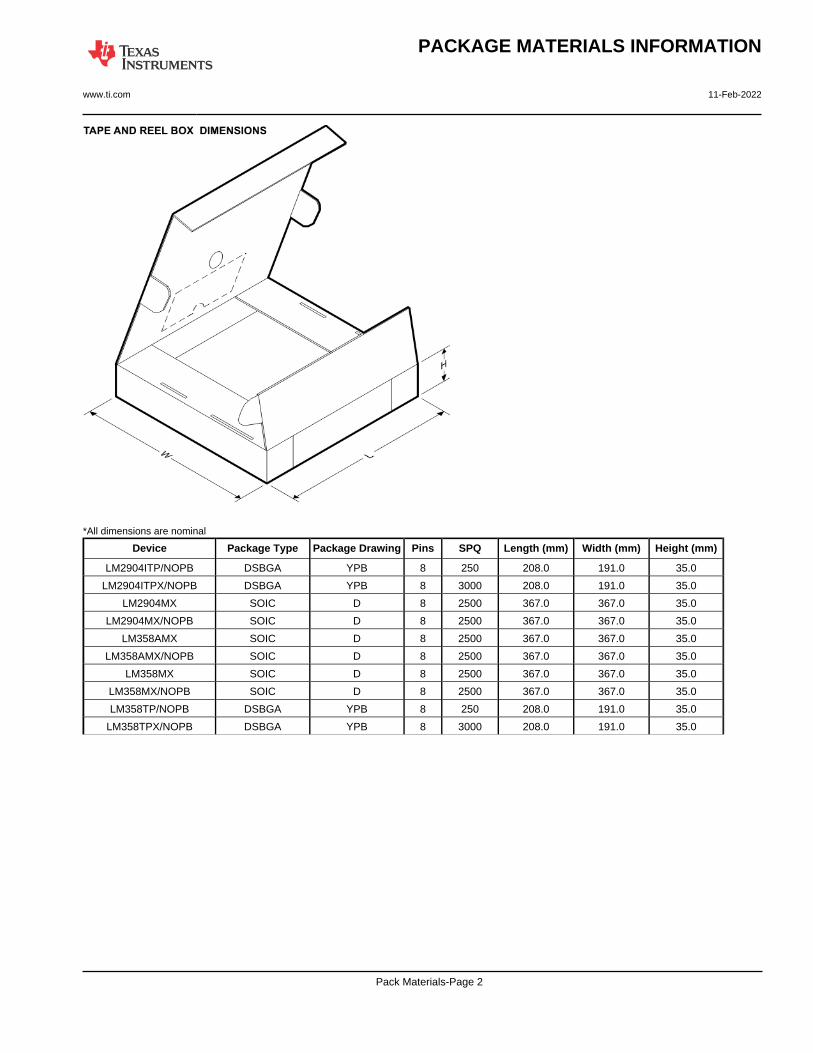
*All dimensions are nominal
Device Package Type Package Drawing Pins SPQ Length (mm) Width (mm) Height (mm)
LM2904ITP/NOPB DSBGA YPB 8 250 208.0 191.0 35.0
LM2904ITPX/NOPB DSBGA YPB 8 3000 208.0 191.0 35.0
LM2904MX SOIC D 8 2500 367.0 367.0 35.0
LM2904MX/NOPB SOIC D 8 2500 367.0 367.0 35.0
LM358AMX SOIC D 8 2500 367.0 367.0 35.0
LM358AMX/NOPB SOIC D 8 2500 367.0 367.0 35.0
LM358MX SOIC D 8 2500 367.0 367.0 35.0
LM358MX/NOPB SOIC D 8 2500 367.0 367.0 35.0
LM358TP/NOPB DSBGA YPB 8 250 208.0 191.0 35.0
LM358TPX/NOPB DSBGA YPB 8 3000 208.0 191.0 35.0
PACKAGE MATERIALS INFORMATION
www.ti.com 11-Feb-2022
Pack Materials-Page 2
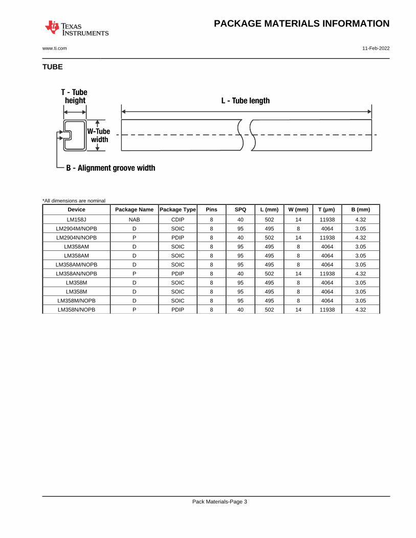
TUBE
*All dimensions are nominal
Device Package Name Package Type Pins SPQ L (mm) W (mm) T (µm) B (mm)
LM158J NAB CDIP 8 40 502 14 11938 4.32
LM2904M/NOPB D SOIC 8 95 495 8 4064 3.05
LM2904N/NOPB P PDIP 8 40 502 14 11938 4.32
LM358AM D SOIC 8 95 495 8 4064 3.05
LM358AM D SOIC 8 95 495 8 4064 3.05
LM358AM/NOPB D SOIC 8 95 495 8 4064 3.05
LM358AN/NOPB P PDIP 8 40 502 14 11938 4.32
LM358M D SOIC 8 95 495 8 4064 3.05
LM358M D SOIC 8 95 495 8 4064 3.05
LM358M/NOPB D SOIC 8 95 495 8 4064 3.05
LM358N/NOPB P PDIP 8 40 502 14 11938 4.32
PACKAGE MATERIALS INFORMATION
www.ti.com 11-Feb-2022
Pack Materials-Page 3
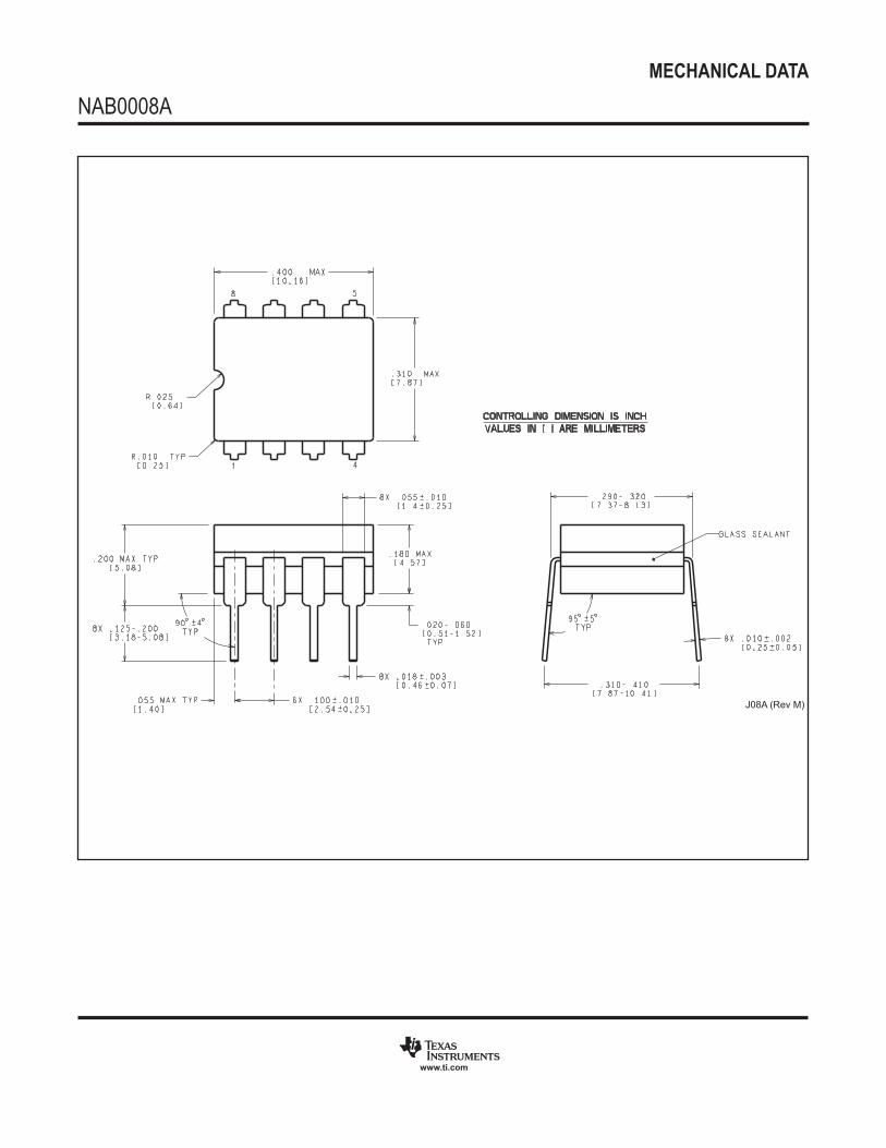
MECHANICAL DATA
NAB0008A
www.ti.com
J08A (Rev M)

www.ti.com
PACKAGE OUTLINE
C
.228-.244 TYP[5.80-6.19]
.069 MAX[1.75]
6X .050[1.27]
8X .012-.020 [0.31-0.51]
2X.150[3.81]
.005-.010 TYP[0.13-0.25]
0 - 8 .004-.010[0.11-0.25]
.010[0.25]
.016-.050[0.41-1.27]
4X (0 -15 )
A
.189-.197[4.81-5.00]
NOTE 3
B .150-.157[3.81-3.98]
NOTE 4
4X (0 -15 )
(.041)[1.04]
SOIC - 1.75 mm max heightD0008ASMALL OUTLINE INTEGRATED CIRCUIT
4214825/C 02/2019
NOTES: 1. Linear dimensions are in inches [millimeters]. Dimensions in parenthesis are for reference only. Controlling dimensions are in inches. Dimensioning and tolerancing per ASME Y14.5M. 2. This drawing is subject to change without notice. 3. This dimension does not include mold flash, protrusions, or gate burrs. Mold flash, protrusions, or gate burrs shall not exceed .006 [0.15] per side. 4. This dimension does not include interlead flash.5. Reference JEDEC registration MS-012, variation AA.
18
.010 [0.25] C A B
54
PIN 1 ID AREA
SEATING PLANE
.004 [0.1] C
SEE DETAIL A
DETAIL ATYPICAL
SCALE 2.800
www.ti.com
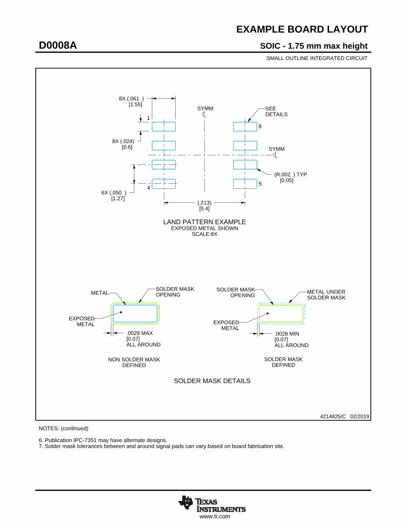
EXAMPLE BOARD LAYOUT
.0028 MAX[0.07]ALL AROUND
.0028 MIN[0.07]ALL AROUND
(.213)[5.4]
6X (.050 )[1.27]
8X (.061 )[1.55]
8X (.024)[0.6]
(R.002 ) TYP[0.05]
SOIC - 1.75 mm max heightD0008ASMALL OUTLINE INTEGRATED CIRCUIT
4214825/C 02/2019
NOTES: (continued) 6. Publication IPC-7351 may have alternate designs. 7. Solder mask tolerances between and around signal pads can vary based on board fabrication site.
METALSOLDER MASKOPENING
NON SOLDER MASKDEFINED
SOLDER MASK DETAILS
EXPOSEDMETAL
OPENINGSOLDER MASK METAL UNDER
SOLDER MASK
SOLDER MASKDEFINED
EXPOSEDMETAL
LAND PATTERN EXAMPLEEXPOSED METAL SHOWN
SCALE:8X
SYMM
1
45
8
SEEDETAILS
SYMM
www.ti.com
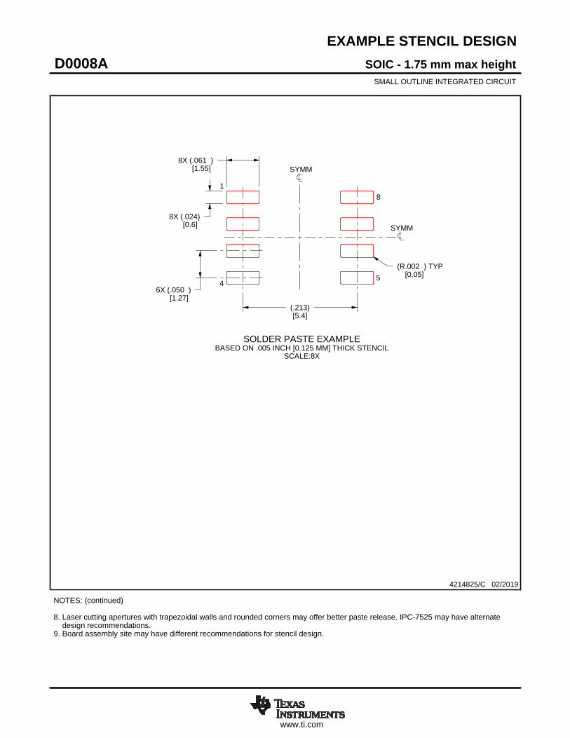
EXAMPLE STENCIL DESIGN
8X (.061 )[1.55]
8X (.024)[0.6]
6X (.050 )[1.27]
(.213)[5.4]
(R.002 ) TYP[0.05]
SOIC - 1.75 mm max heightD0008ASMALL OUTLINE INTEGRATED CIRCUIT
4214825/C 02/2019
NOTES: (continued) 8. Laser cutting apertures with trapezoidal walls and rounded corners may offer better paste release. IPC-7525 may have alternate design recommendations. 9. Board assembly site may have different recommendations for stencil design.
SOLDER PASTE EXAMPLEBASED ON .005 INCH [0.125 MM] THICK STENCIL
SCALE:8X
SYMM
SYMM
1
45
8
www.ti.com
PACKAGE OUTLINE
C0.575 MAX
0.150.11
1TYP
1TYP
8X 0.180.16
0.5TYP
0.5TYP
B E A
D
4215100/B 07/2016
DSBGA - 0.575 mm max heightYPB0008DIE SIZE BALL GRID ARRAY
NOTES: 1. All linear dimensions are in millimeters. Any dimensions in parenthesis are for reference only. Dimensioning and tolerancing per ASME Y14.5M.2. This drawing is subject to change without notice.
SYMM
SYMM
BALL A1CORNER
SEATING PLANE
BALL TYP0.05 C
1 2
0.015 C A B
A
B
C
3
SCALE 9.000
D: Max =
E: Max =
1.337 mm, Min =
1.337 mm, Min =
1.276 mm
1.276 mm
www.ti.com
EXAMPLE BOARD LAYOUT
8X ( 0.16)
( 0.16)METAL
0.05 MAX
SOLDER MASKOPENING
METAL UNDERSOLDER MASK
( 0.16)SOLDER MASKOPENING
0.05 MIN
(0.5) TYP
(0.5)TYP
4215100/B 07/2016
DSBGA - 0.575 mm max heightYPB0008DIE SIZE BALL GRID ARRAY
NOTES: (continued) 3. Final dimensions may vary due to manufacturing tolerance considerations and also routing constraints. See Texas Instruments Literature No. SNVA009 (www.ti.com/lit/snva009).
SOLDER MASK DETAILSNOT TO SCALE
1 2
A
B
SYMM
SYMM
LAND PATTERN EXAMPLESCALE:40X
C
3
NON-SOLDER MASKDEFINED
(PREFERRED)SOLDER MASK
DEFINED
www.ti.com
EXAMPLE STENCIL DESIGN
8X ( 0.3) (R0.05) TYP
METALTYP
(0.5) TYP
(0.5) TYP
4215100/B 07/2016
DSBGA - 0.575 mm max heightYPB0008DIE SIZE BALL GRID ARRAY
NOTES: (continued) 4. Laser cutting apertures with trapezoidal walls and rounded corners may offer better paste release.
1 2
A
B
C
3
SYMM
SYMM
SOLDER PASTE EXAMPLEBASED ON 0.125mm THICK STENCIL
SCALE:50X
IMPORTANT NOTICE AND DISCLAIMERTI PROVIDES TECHNICAL AND RELIABILITY DATA (INCLUDING DATA SHEETS), DESIGN RESOURCES (INCLUDING REFERENCE DESIGNS), APPLICATION OR OTHER DESIGN ADVICE, WEB TOOLS, SAFETY INFORMATION, AND OTHER RESOURCES “AS IS” AND WITH ALL FAULTS, AND DISCLAIMS ALL WARRANTIES, EXPRESS AND IMPLIED, INCLUDING WITHOUT LIMITATION ANY IMPLIED WARRANTIES OF MERCHANTABILITY, FITNESS FOR A PARTICULAR PURPOSE OR NON-INFRINGEMENT OF THIRD PARTY INTELLECTUAL PROPERTY RIGHTS.These resources are intended for skilled developers designing with TI products. You are solely responsible for (1) selecting the appropriate TI products for your application, (2) designing, validating and testing your application, and (3) ensuring your application meets applicable standards, and any other safety, security, regulatory or other requirements.These resources are subject to change without notice. TI grants you permission to use these resources only for development of an application that uses the TI products described in the resource. Other reproduction and display of these resources is prohibited. No license is granted to any other TI intellectual property right or to any third party intellectual property right. TI disclaims responsibility for, and you will fully indemnify TI and its representatives against, any claims, damages, costs, losses, and liabilities arising out of your use of these resources.TI’s products are provided subject to TI’s Terms of Sale or other applicable terms available either on ti.com or provided in conjunction with such TI products. TI’s provision of these resources does not expand or otherwise alter TI’s applicable warranties or warranty disclaimers for TI products.TI objects to and rejects any additional or different terms you may have proposed. IMPORTANT NOTICE
Mailing Address: Texas Instruments, Post Office Box 655303, Dallas, Texas 75265Copyright © 2022, Texas Instruments Incorporated